Embed Size (px)
Citation preview
Common magnetoresistance measurements: AMR, GMR, AHE/SHE, TMR
Department of Physics and ChemistryC4S/ Technical University
Cluj‐Napoca, Romania
CNRS‐Université de LorraineNancy, France
Prof. Dr. Coriolan TIUSAN
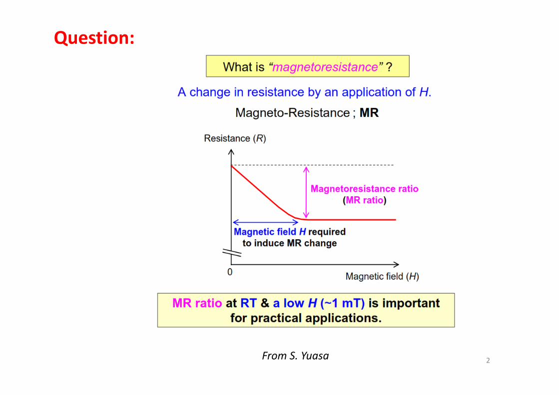
From S. Yuasa 2
Question:
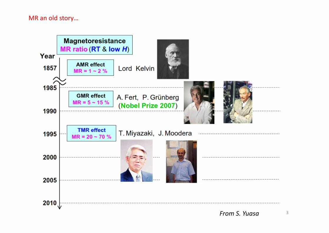
From S. Yuasa 3
MR an old story…
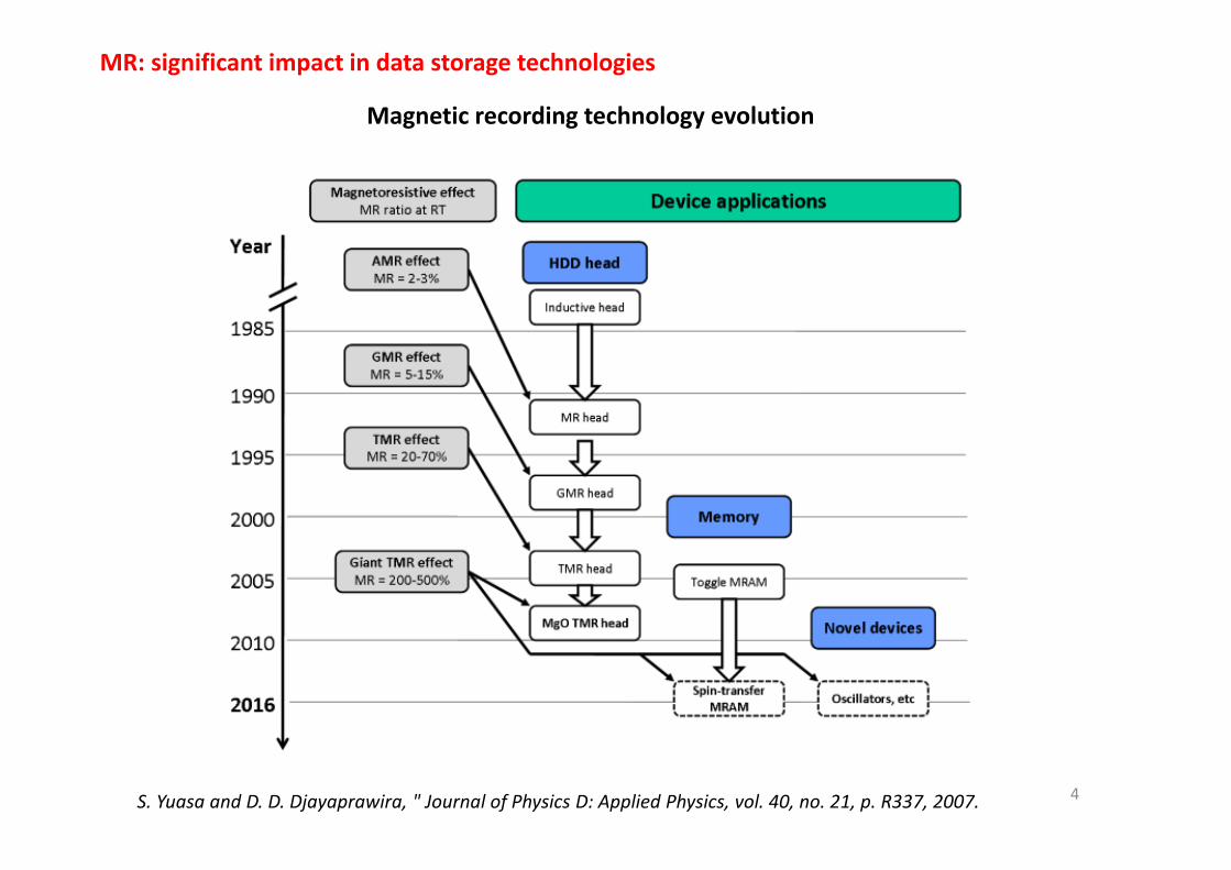
S. Yuasa and D. D. Djayaprawira, " Journal of Physics D: Applied Physics, vol. 40, no. 21, p. R337, 2007.
Magnetic recording technology evolution
4
MR: significant impact in data storage technologies
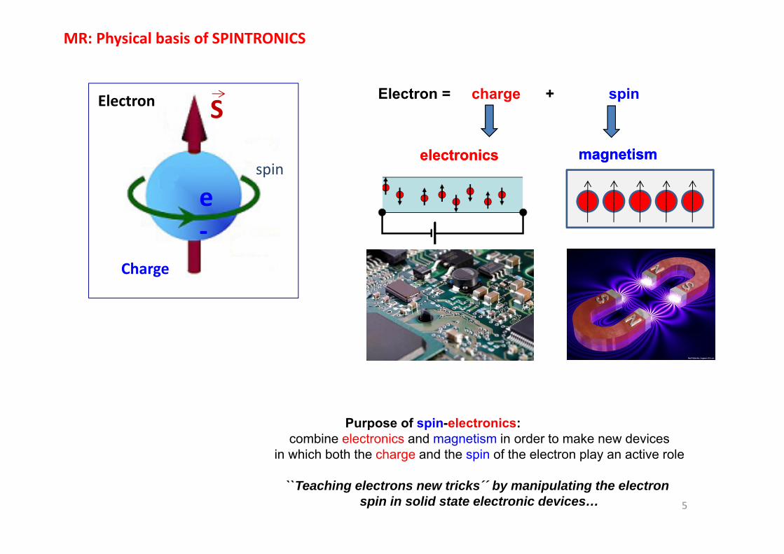
Electron = charge + spin
electronics magnetism
Charge
spin
e‐
S
Purpose of spin-electronics: combine electronics and magnetism in order to make new devices
in which both the charge and the spin of the electron play an active role
``Teaching electrons new tricks´´ by manipulating the electron spin in solid state electronic devices…
Electron
electronics magnetism
MR: Physical basis of SPINTRONICS
5
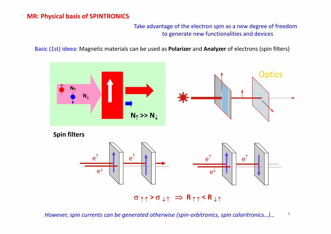
Take advantage of the electron spin as a new degree of freedomto generate new functionalities and devices
Basic (1st) ideea: Magnetic materials can be used as Polarizer and Analyzer of electrons (spin filters)
N
N
N>> N
Optics
ee e
ee e
> R < R
Spin filters
However, spin currents can be generated otherwise (spin‐orbitronics, spin caloritronics…)… 6
MR: Physical basis of SPINTRONICS
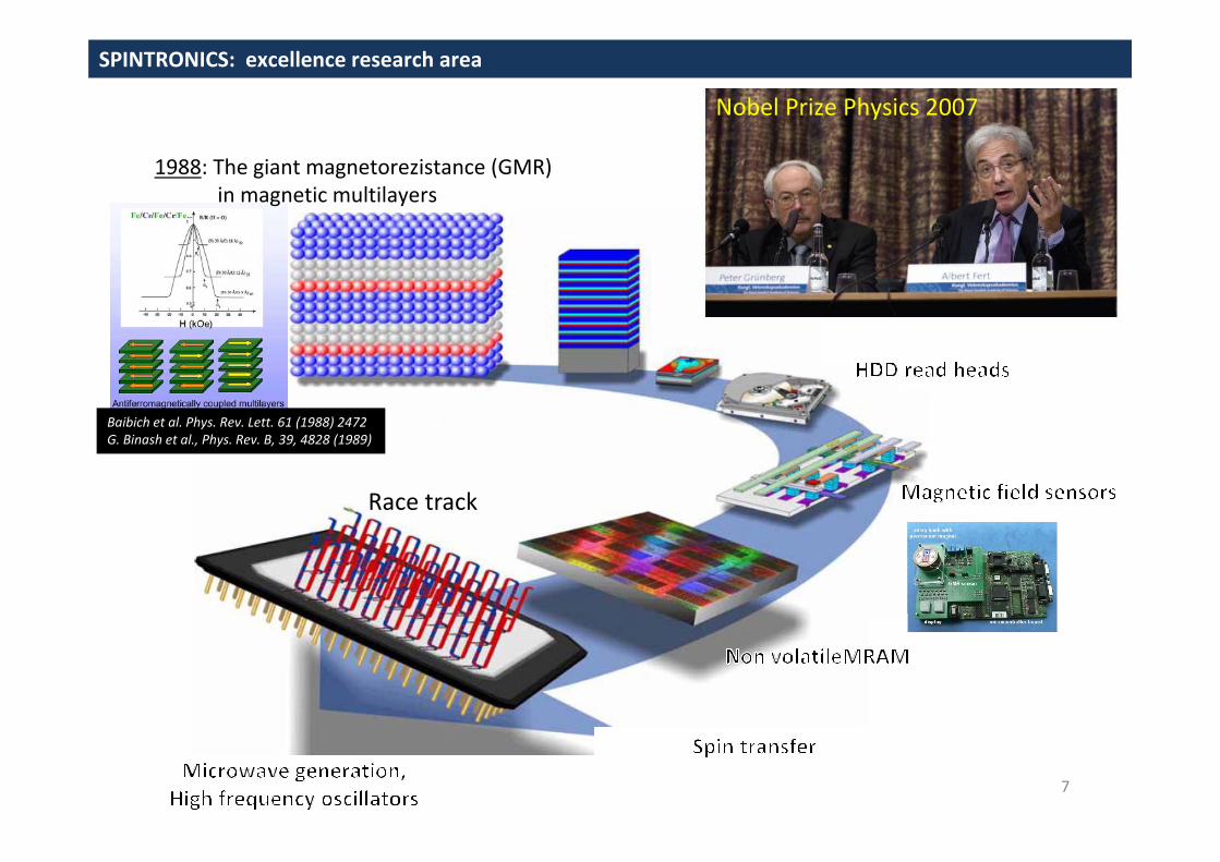
Baibich et al. Phys. Rev. Lett. 61 (1988) 2472 G. Binash et al., Phys. Rev. B, 39, 4828 (1989)
Nobel Prize Physics 2007
1988: The giant magnetorezistance (GMR) in magnetic multilayers
SPINTRONICS: excellence research area
Race track
7
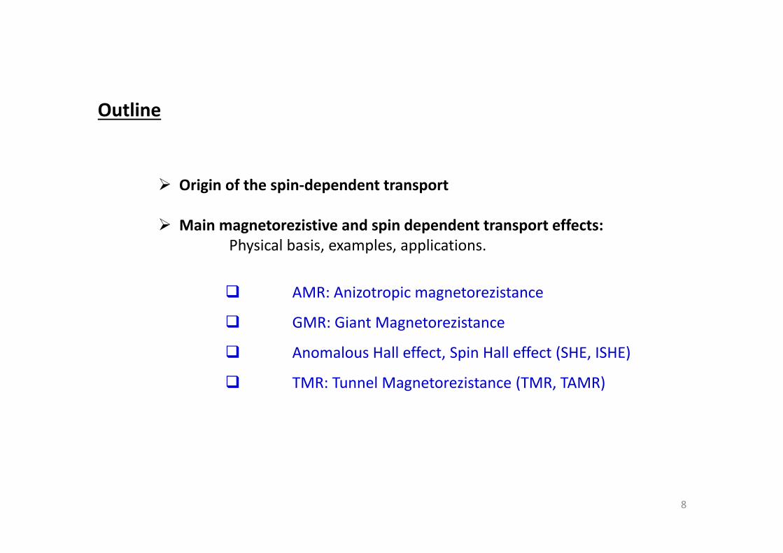
Outline
Origin of the spin‐dependent transport
Main magnetorezistive and spin dependent transport effects:Physical basis, examples, applications.
AMR: Anizotropic magnetorezistance
GMR: Giant Magnetorezistance
Anomalous Hall effect, Spin Hall effect (SHE, ISHE)
TMR: Tunnel Magnetorezistance (TMR, TAMR)
8
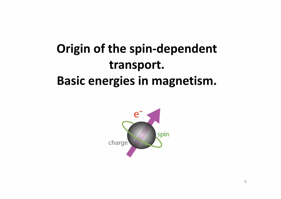
Origin of the spin‐dependent transport.
Basic energies in magnetism.
9
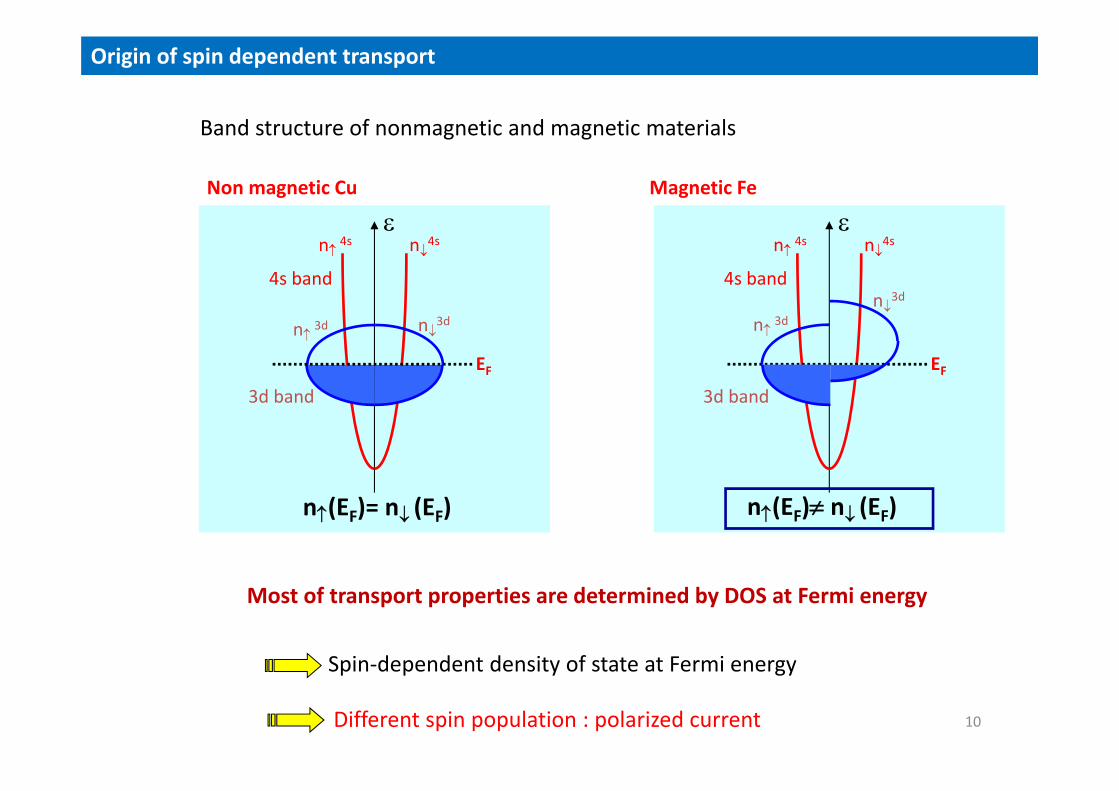
Band structure of nonmagnetic and magnetic materials
EF3d band
4s band
n(EF)= n (EF)
n3d
n 4s n4s
n 3d
EF3d band
4s band
n(EF) n (EF)
n3d
n 4s n4s
n 3d
Non magnetic Cu Magnetic Fe
Most of transport properties are determined by DOS at Fermi energy
Spin‐dependent density of state at Fermi energy
Different spin population : polarized current
Origin of spin dependent transport
10
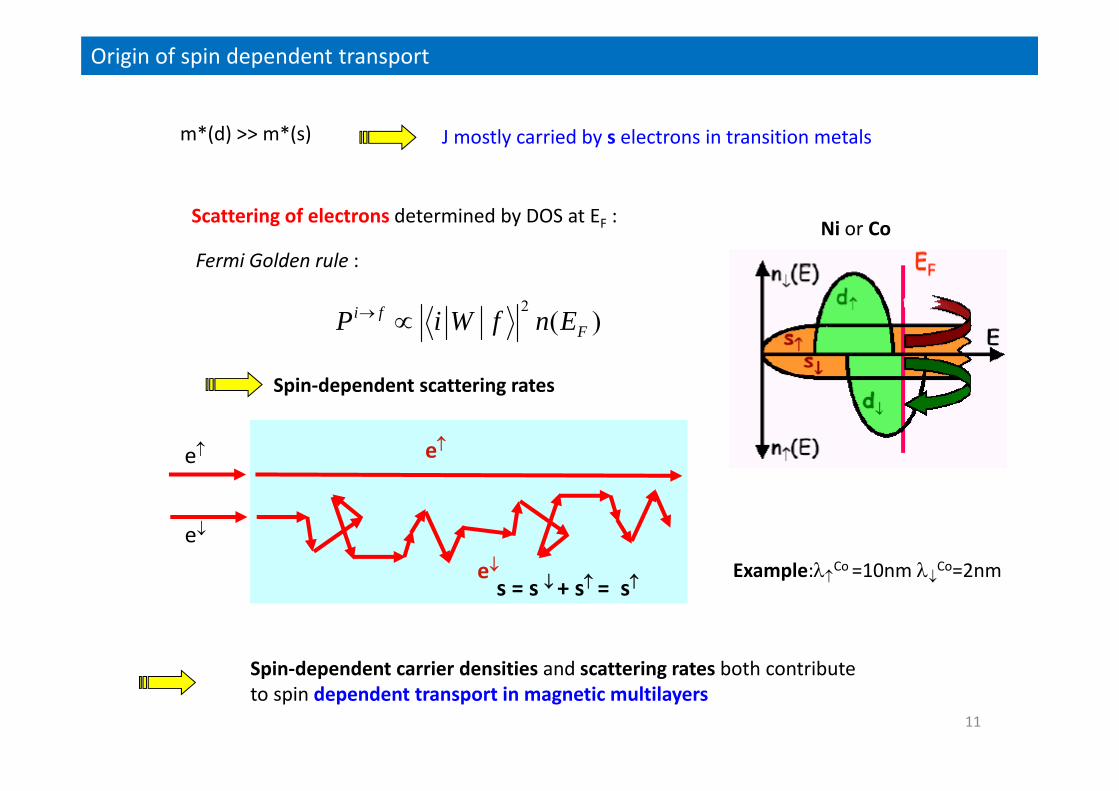
m*(d) >> m*(s) J mostly carried by s electrons in transition metals
Scattering of electrons determined by DOS at EF :
Fermi Golden rule :
2( )i f
FP i W f n E
Ni or Co
Spin‐dependent scattering rates
Example:Co =10nm Co=2nm
Spin‐dependent carrier densities and scattering rates both contributeto spin dependent transport in magnetic multilayers
e
e
e
es = s + s = s
Origin of spin dependent transport
11
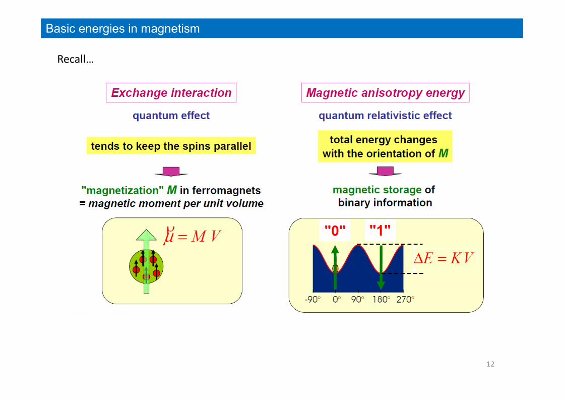
Basic energies in magnetism
12
Recall…
AMR: Anizotropic magnetorezistance
GMR: Giant Magnetorezistance
AHE: Anomalous Hall effect
TMR: Tunnel Magnetorezistance (TMR, TAMR, …)
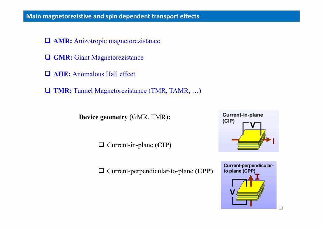
Main magnetorezistive and spin dependent transport effects
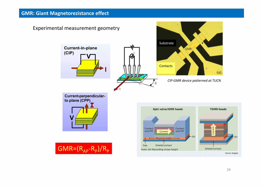
Device geometry (GMR, TMR):
Current-in-plane (CIP)
Current-perpendicular-to-plane (CPP)
13
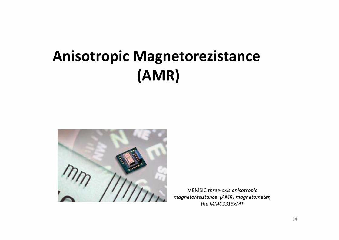
Anisotropic Magnetorezistance (AMR)
MEMSIC three‐axis anisotropic magnetoresistance (AMR) magnetometer,
the MMC3316xMT
14
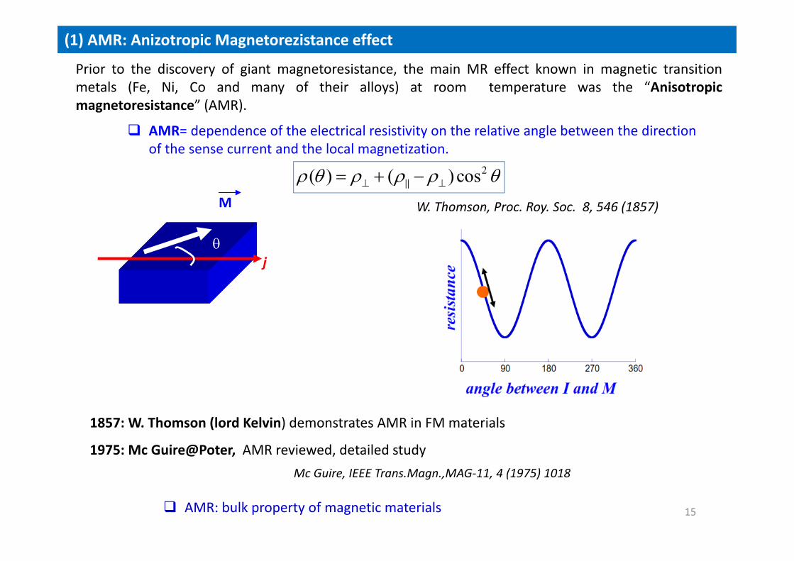
1857: W. Thomson (lord Kelvin) demonstrates AMR in FM materials
1975: Mc Guire@Poter, AMR reviewed, detailed studyMc Guire, IEEE Trans.Magn.,MAG‐11, 4 (1975) 1018
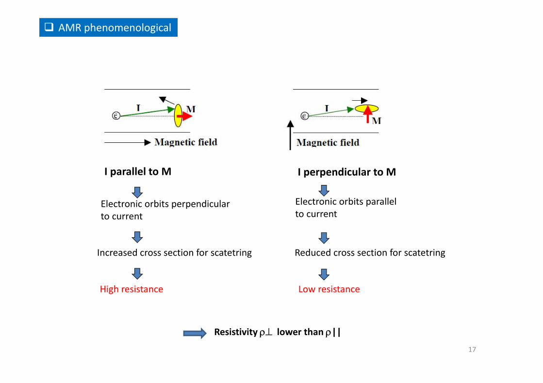
(1) AMR: Anizotropic Magnetorezistance effect
15
Prior to the discovery of giant magnetoresistance, the main MR effect known in magnetic transitionmetals (Fe, Ni, Co and many of their alloys) at room temperature was the “Anisotropicmagnetoresistance” (AMR).
AMR= dependence of the electrical resistivity on the relative angle between the direction of the sense current and the local magnetization.
M
j
2( ) ( ) cos W. Thomson, Proc. Roy. Soc. 8, 546 (1857)
AMR: bulk property of magnetic materials
16
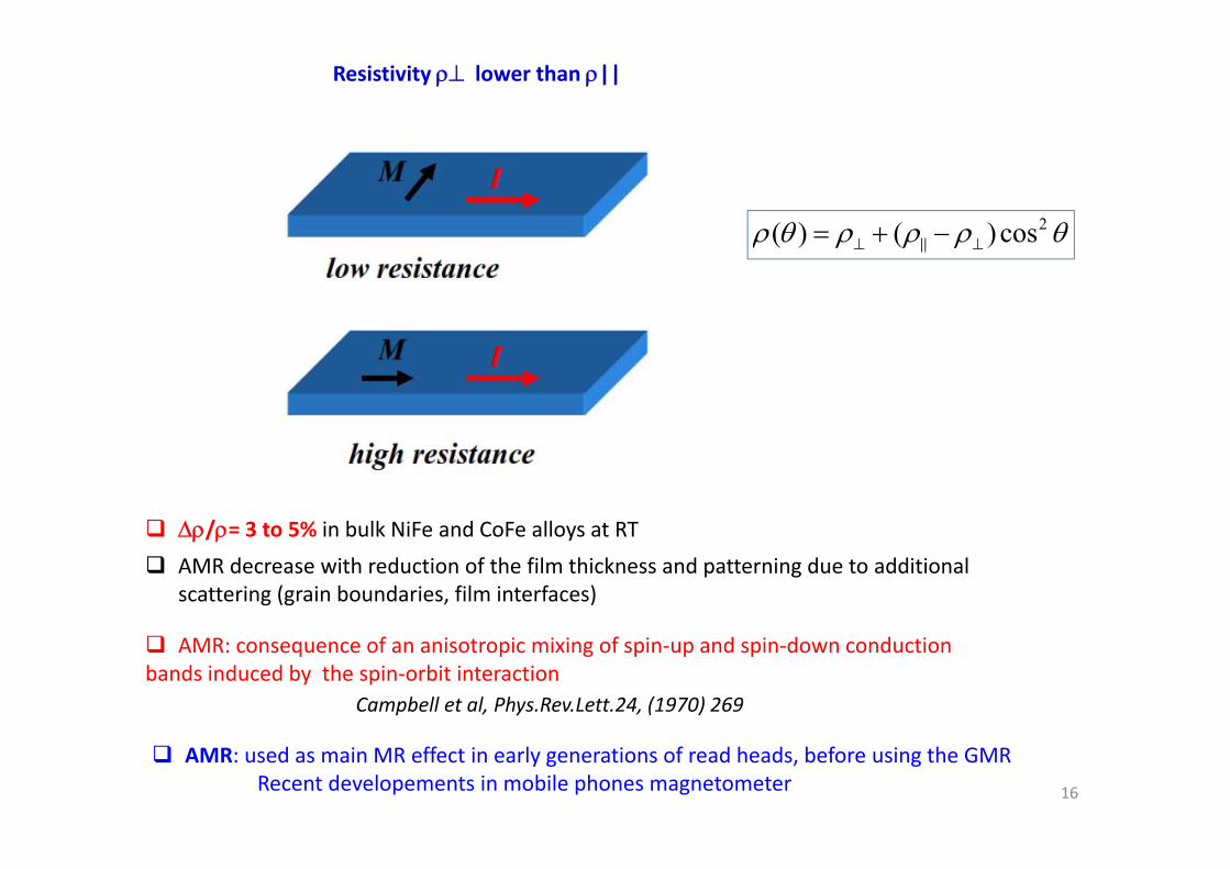
AMR: consequence of an anisotropic mixing of spin‐up and spin‐down conduction bands induced by the spin‐orbit interaction
Campbell et al, Phys.Rev.Lett.24, (1970) 269
AMR: used as main MR effect in early generations of read heads, before using the GMRRecent developements in mobile phones magnetometer
/= 3 to 5% in bulk NiFe and CoFe alloys at RT
AMR decrease with reduction of the film thickness and patterning due to additionalscattering (grain boundaries, film interfaces)
Resistivity lower than ||
2( ) ( ) cos
I parallel to M
Electronic orbits perpendicularto current
Increased cross section for scatetring
High resistance
I perpendicular to M
Electronic orbits parallelto current
Reduced cross section for scatetring
Low resistance
AMR phenomenological
Resistivity lower than ||
17
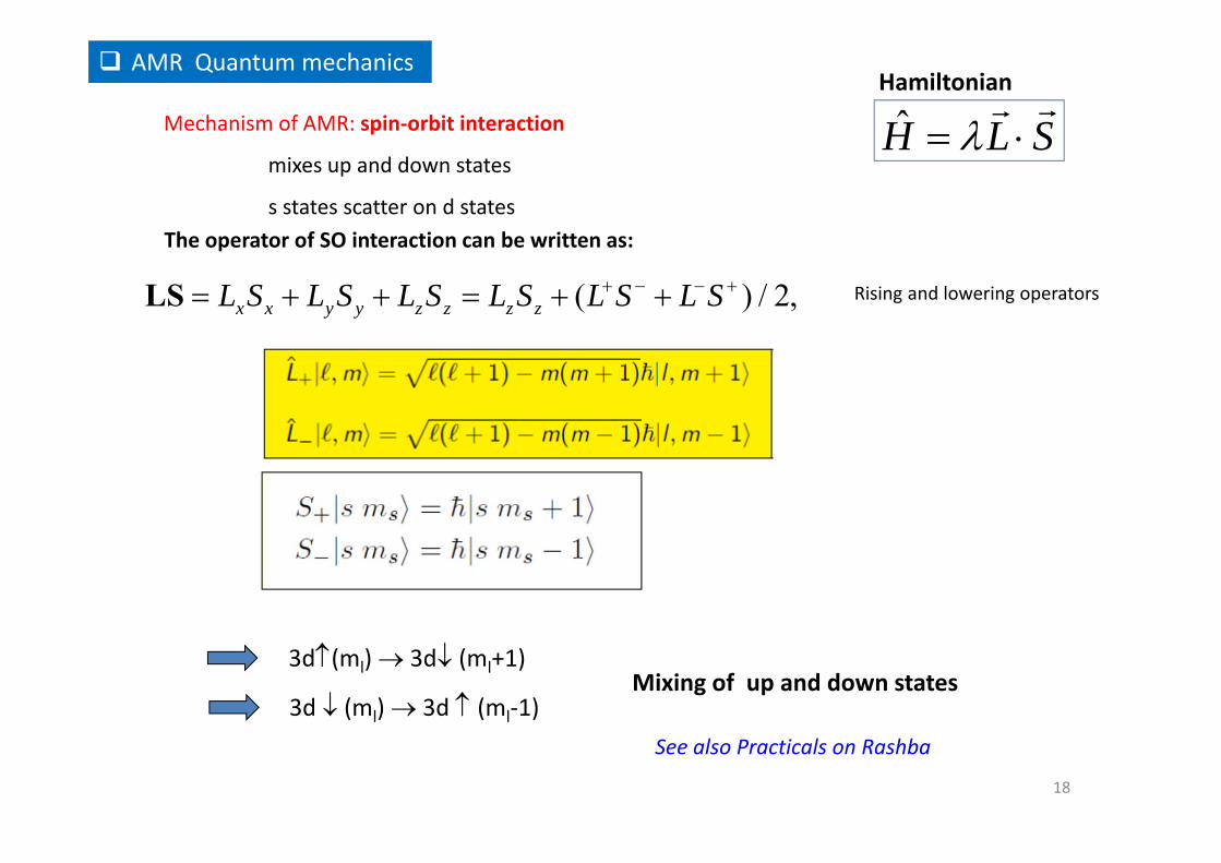
Mechanism of AMR: spin‐orbit interaction
mixes up and down states
s states scatter on d statesThe operator of SO interaction can be written as:
( ) / 2,x x y y z z z zL S L S L S L S L S L S LS
AMR Quantum mechanics
Rising and lowering operators
3d(ml) 3d (ml+1)
3d (ml) 3d (ml‐1) Mixing of up and down states
H L S Hamiltonian
18
See also Practicals on Rashba

Simplified case: Strong ferromagnet no 3d states
LS=0 => only s‐d scattering in down channel allowed , no s d scattering
LS0 => Inclusion of spin‐orbit coupling opens up the possibility of spin‐flip transitions in the s‐dchannels. As a consequence, also the spin‐up channel will now contribute to the conductivity.4s 3d scattering => increase of rezistivity
s d scattering rate depends on the direction of momentum of s electron k
relative to clasical orbit of unocupied orbital d
Clasical orbit: momentum L parallel toM => scattering rate depends on angle between
k andM
19
Exercise(practicals)
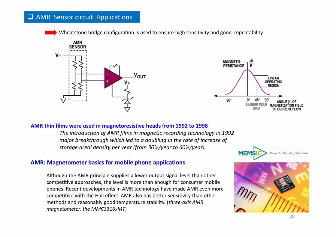
AMR thin films were used in magnetoresistive heads from 1992 to 1998The introduction of AMR films in magnetic recording technology in 1992 major breakthrough which led to a doubling in the rate of increase of storage areal density per year (from 30%/year to 60%/year).
AMR Sensor circuit. Applications
Although the AMR principle supplies a lower output signal level than other competitive approaches, the level is more than enough for consumer mobile phones. Recent developments in AMR technology have made AMR even more competitive with the Hall effect. AMR also has better sensitivity than other methods and reasonably good temperature stability. (three‐axis AMR magnetometer, the MMC3316xMT)
AMR: Magnetometer basics for mobile phone applications
20
Wheatstone bridge configuration is used to ensure high sensitivity and good repeatability
I
M
IM
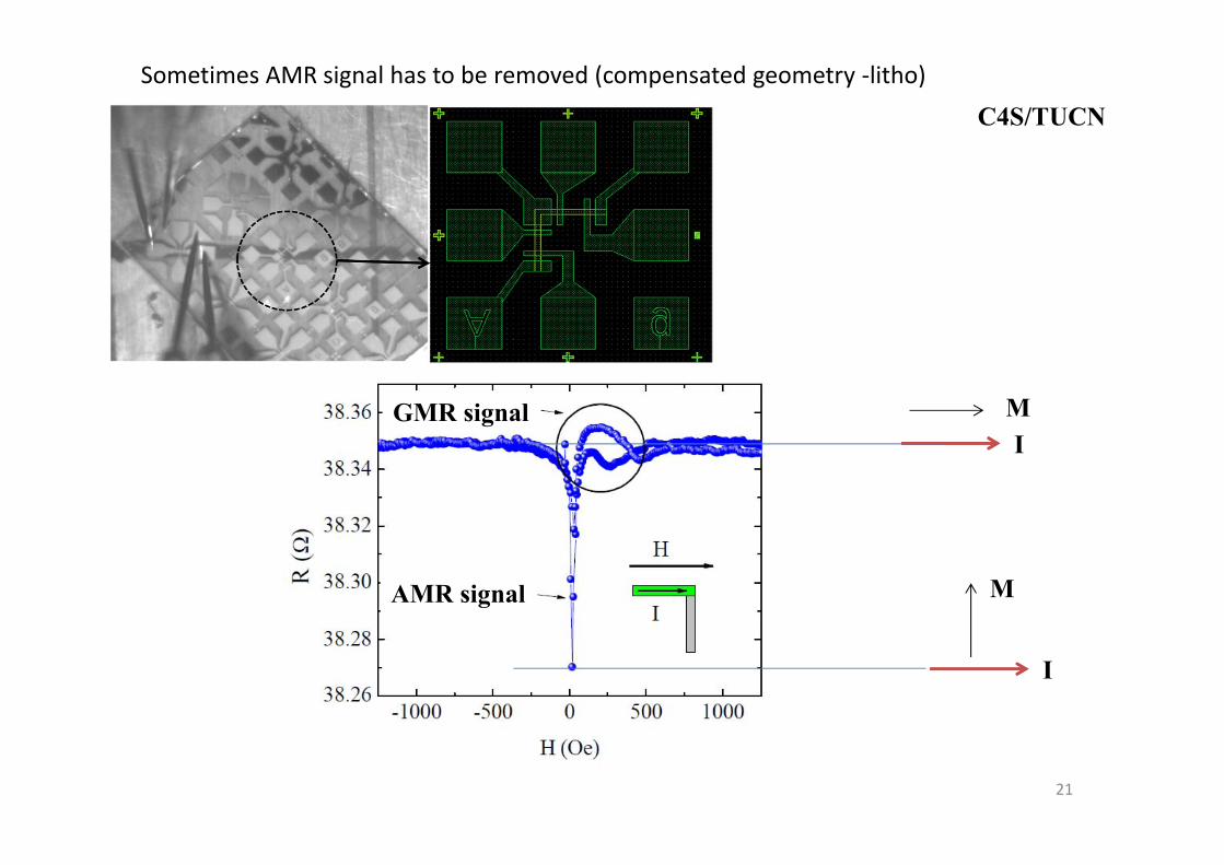
AMR signal
C4S/TUCNSometimes AMR signal has to be removed (compensated geometry ‐litho)
GMR signal
21
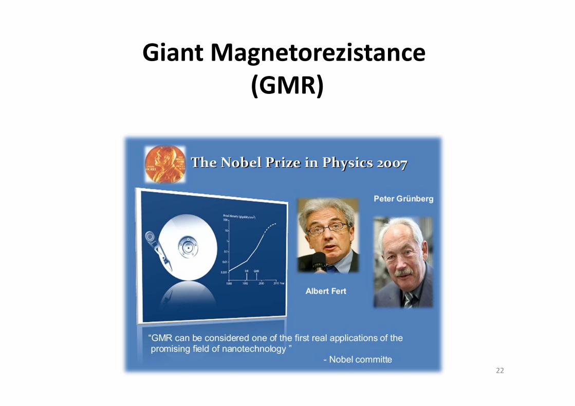
Giant Magnetorezistance (GMR)
22
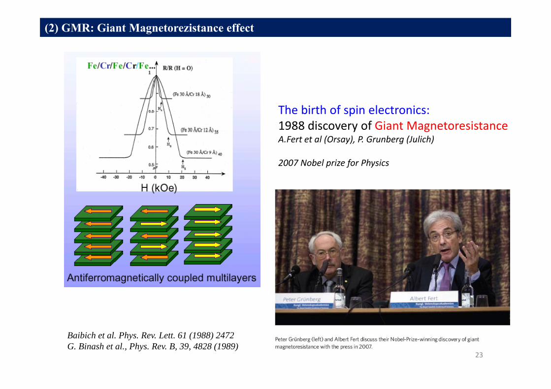
Baibich et al. Phys. Rev. Lett. 61 (1988) 2472 G. Binash et al., Phys. Rev. B, 39, 4828 (1989)
The birth of spin electronics:1988 discovery of Giant MagnetoresistanceA.Fert et al (Orsay), P. Grunberg (Julich)
2007 Nobel prize for Physics
(2) GMR: Giant Magnetorezistance effect
23
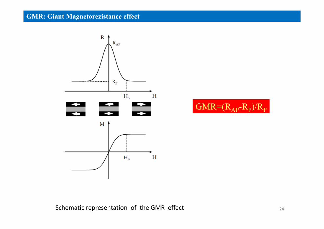
Schematic representation of the GMR effect
GMR=(RAP-RP)/RP
GMR: Giant Magnetorezistance effect
24
),θ
),θcos(22
21 MM
RRRRR appapp
HR low
R high
(1)
(2)
(3)
(4)
(2)
(3)
(4)
(1)
R
M1
M2
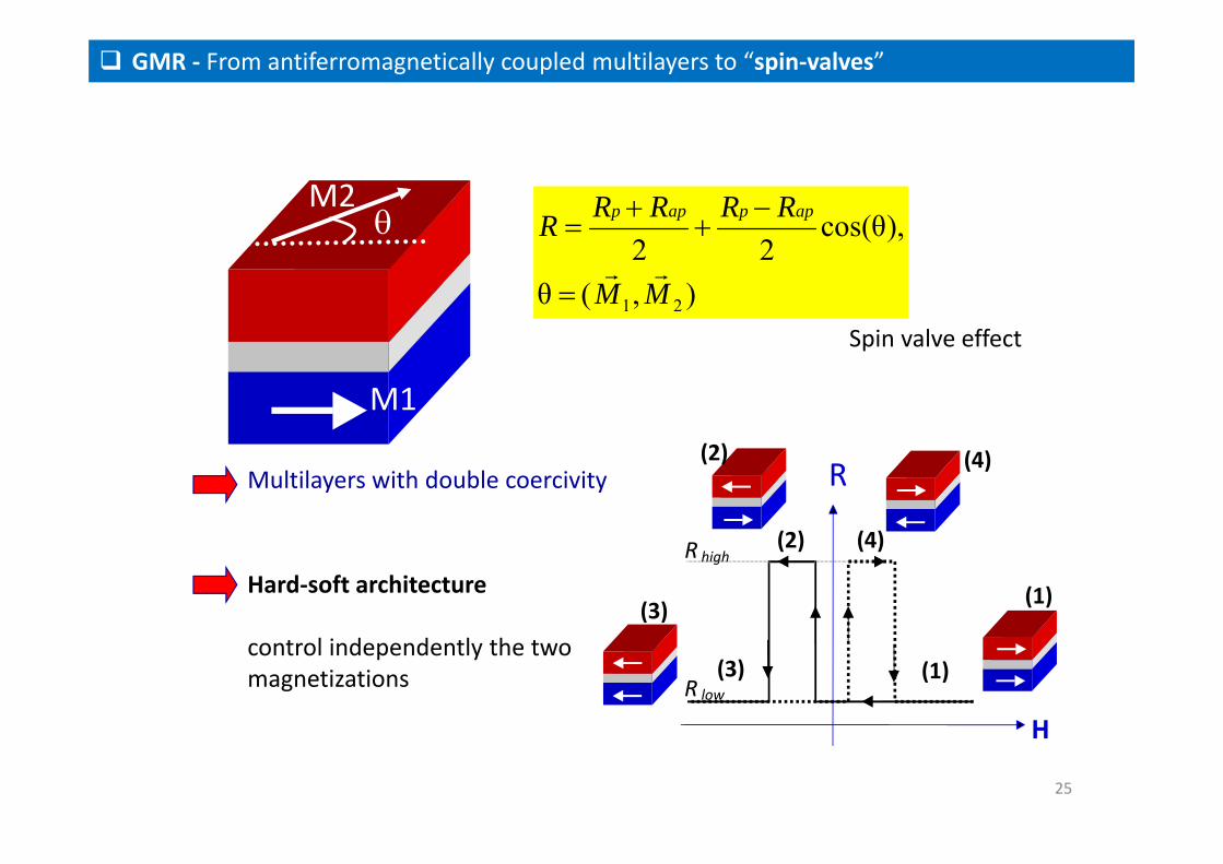
Spin valve effect
Hard‐soft architecture
control independently the twomagnetizations
Multilayers with double coercivity
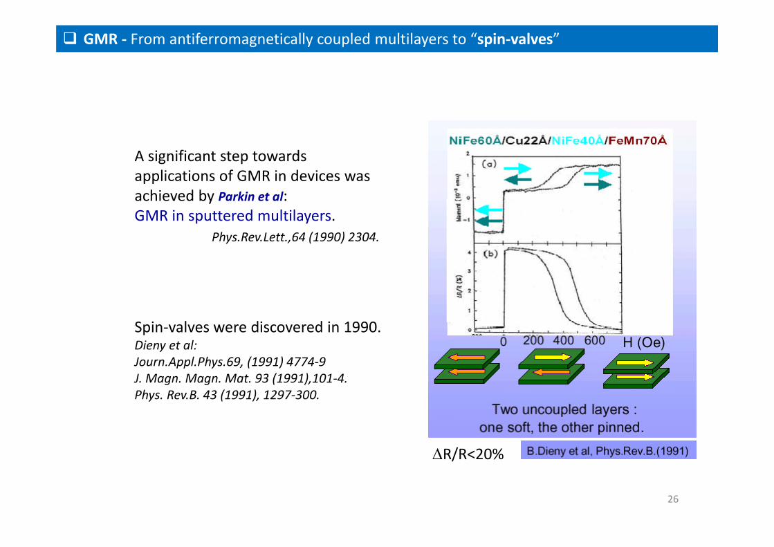
GMR ‐ From antiferromagnetically coupled multilayers to “spin‐valves”
25
R/R<20%
A significant step towardsapplications of GMR in devices was achieved by Parkin et al: GMR in sputtered multilayers.
Spin‐valves were discovered in 1990.Dieny et al:Journ.Appl.Phys.69, (1991) 4774‐9J. Magn. Magn. Mat. 93 (1991),101‐4.Phys. Rev.B. 43 (1991), 1297‐300.
Phys.Rev.Lett.,64 (1990) 2304.
GMR ‐ From antiferromagnetically coupled multilayers to “spin‐valves”
26
-400 -200 0 200 400
0
3
6
9
12
GM
R (%
)
H (Oe)
3-300
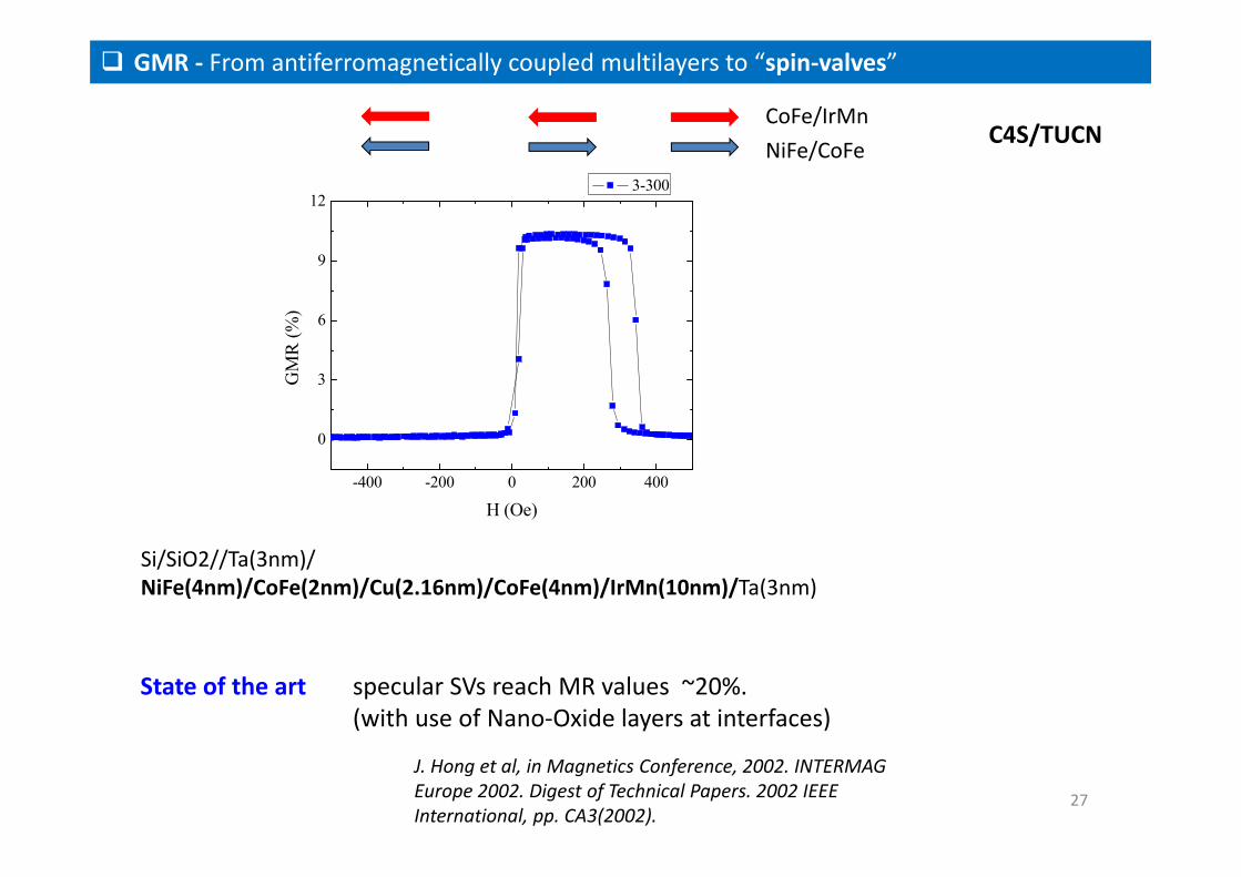
Si/SiO2//Ta(3nm)/NiFe(4nm)/CoFe(2nm)/Cu(2.16nm)/CoFe(4nm)/IrMn(10nm)/Ta(3nm)
NiFe/CoFeCoFe/IrMn
C4S/TUCN
GMR ‐ From antiferromagnetically coupled multilayers to “spin‐valves”
27
State of the art specular SVs reach MR values ~20%. (with use of Nano‐Oxide layers at interfaces)
J. Hong et al, in Magnetics Conference, 2002. INTERMAG Europe 2002. Digest of Technical Papers. 2002 IEEE International, pp. CA3(2002).
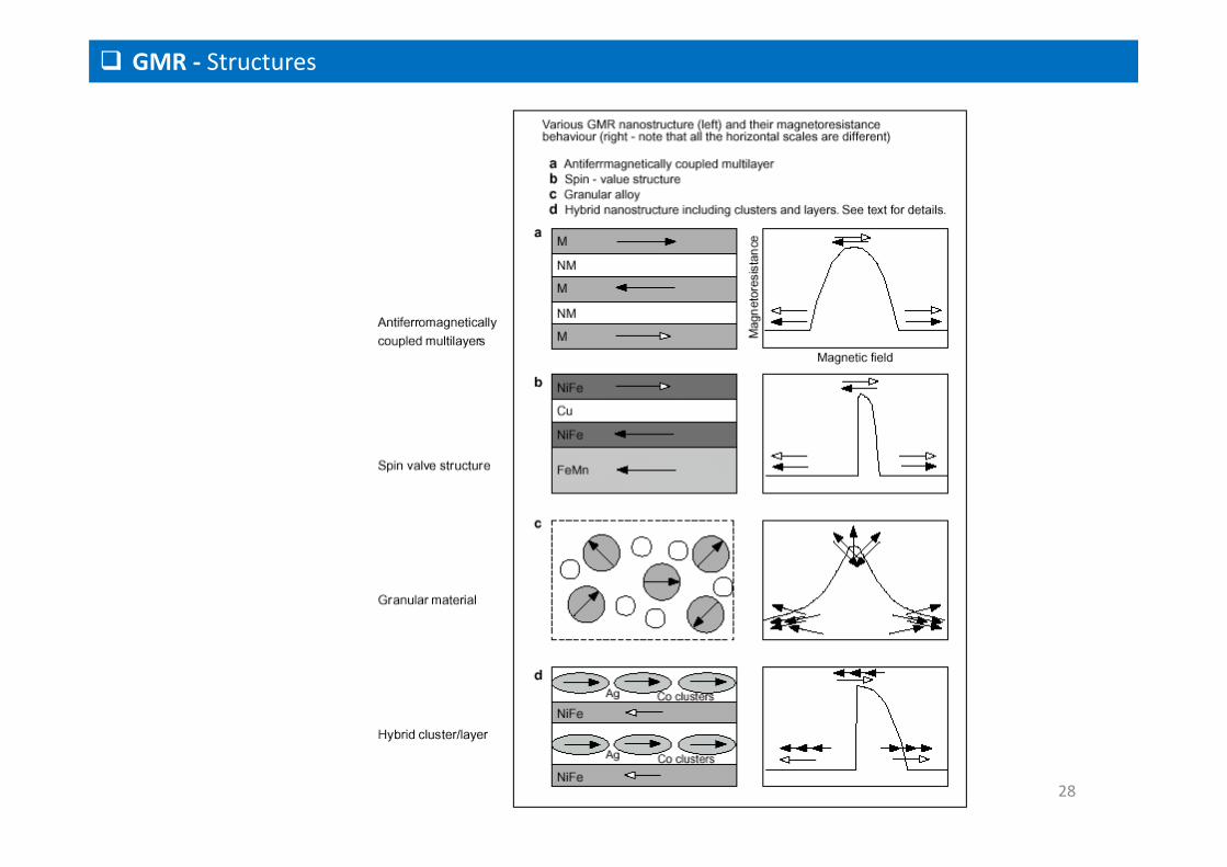
GMR ‐ Structures
28
GMR=(RAP‐RP)/RP
Experimental measurement geometry
GMR: Giant Magnetorezistance effect
Contacts
Substrate
CIP‐GMR device patterned at TUCN
29
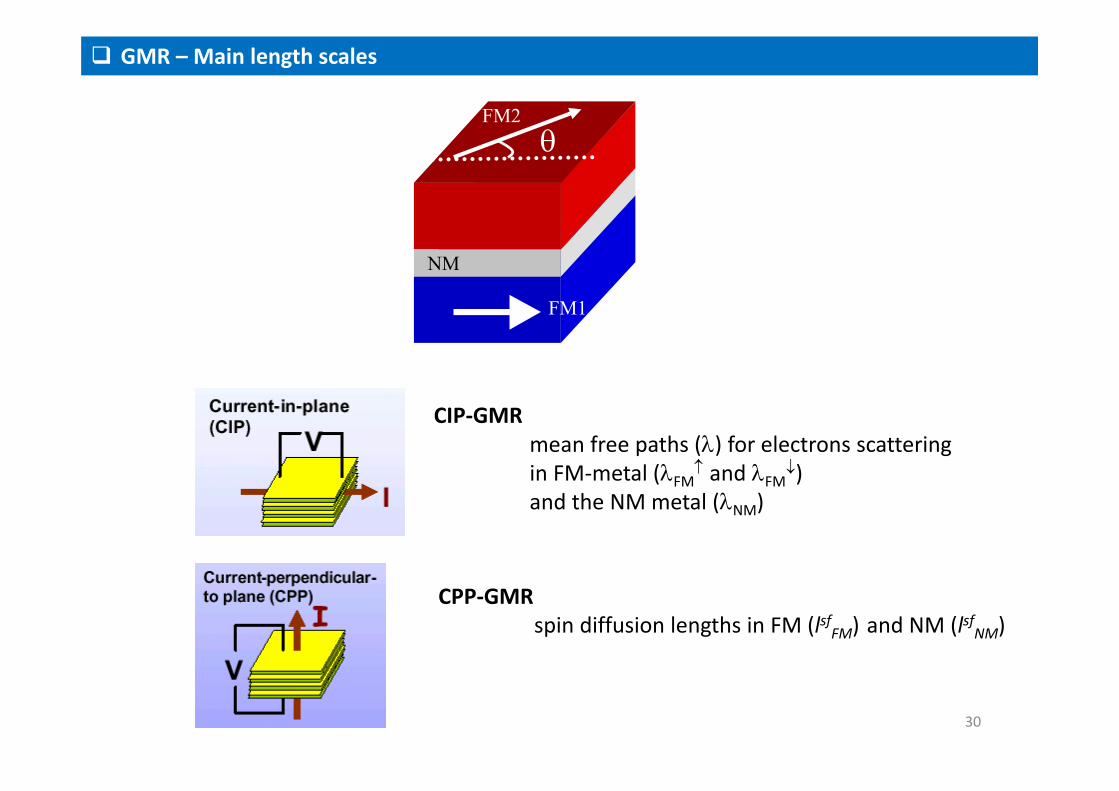
GMR – Main length scales
CIP‐GMRmean free paths () for electrons scatteringin FM‐metal (FM and FM) and the NM metal (NM)
FM1
FM2
NM
CPP‐GMRspin diffusion lengths in FM (lsfFM) and NM (lsfNM)
30
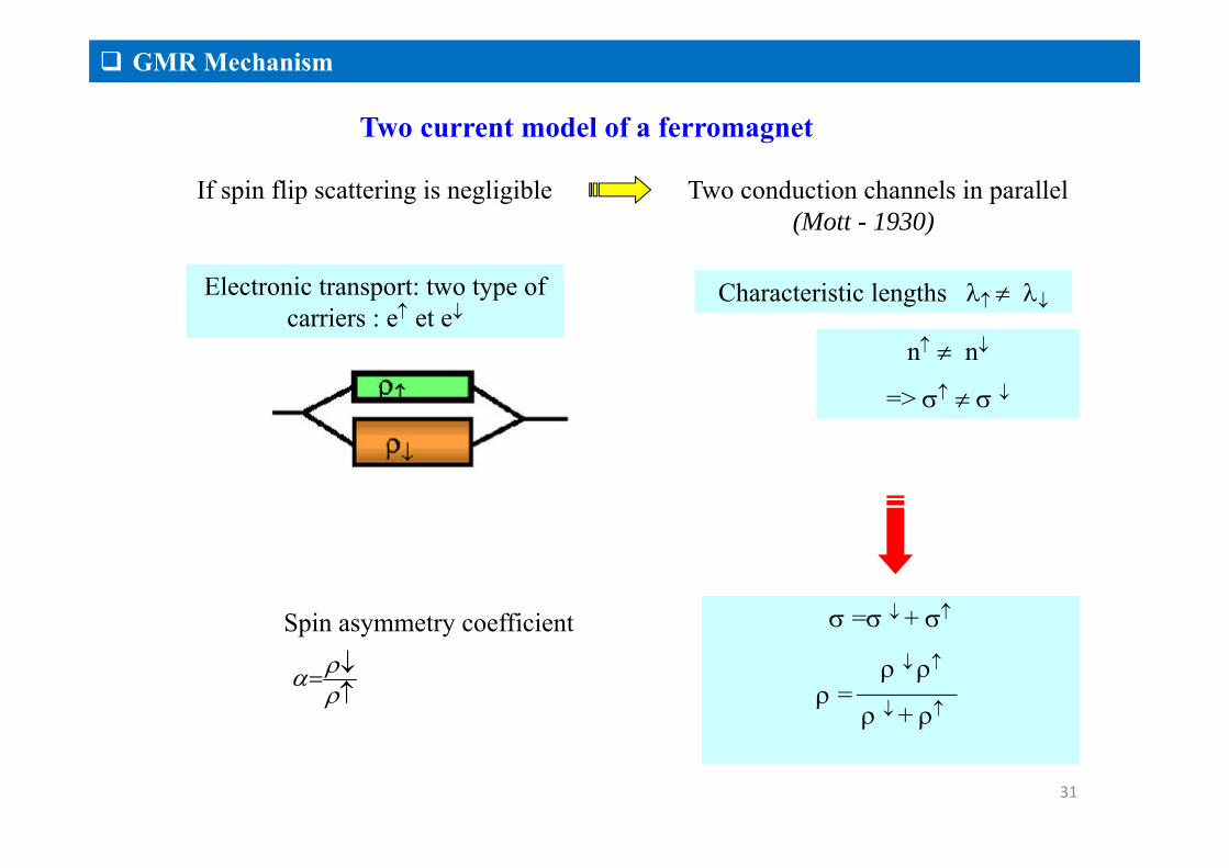
If spin flip scattering is negligible Two conduction channels in parallel (Mott - 1930)
Electronic transport: two type of carriers : e et e
Characteristic lengths
n n
=>
= +
+ =
Spin asymmetry coefficient
Two current model of a ferromagnet
GMR Mechanism
31
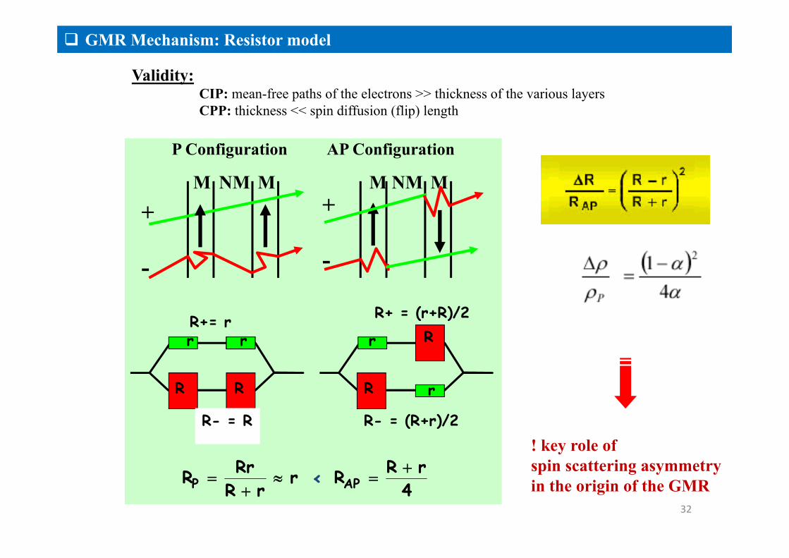
Validity:CIP: mean-free paths of the electrons >> thickness of the various layersCPP: thickness << spin diffusion (flip) length
r r
r
r
R R R
RR+= r
R- = R
R+ = (r+R)/2
R- = (R+r)/2
rrR
RrRP
4
rRRAP
<
P Configuration AP Configuration
M MNM M MNM
-
+
-
+
! key role of spin scattering asymmetry in the origin of the GMR
GMR Mechanism: Resistor model
32
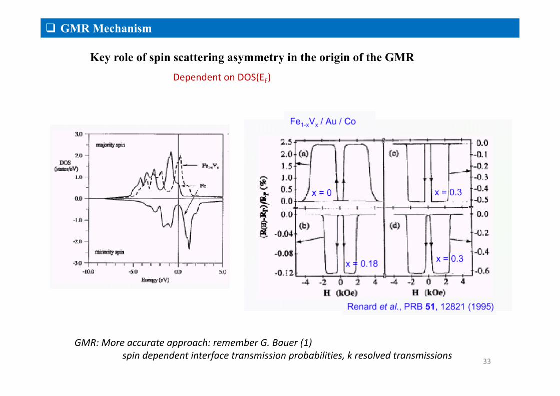
Key role of spin scattering asymmetry in the origin of the GMR
GMR Mechanism
33
GMR: More accurate approach: remember G. Bauer (1)spin dependent interface transmission probabilities, k resolved transmissions
Dependent on DOS(EF)
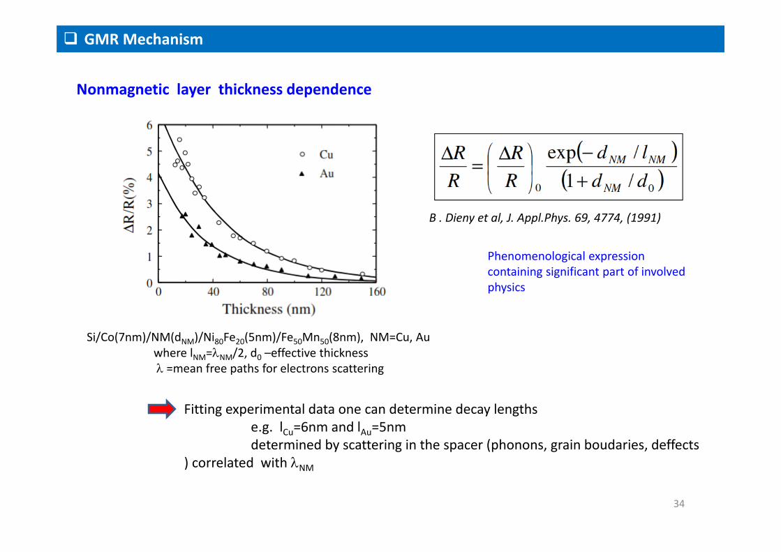
Nonmagnetic layer thickness dependence
B . Dieny et al, J. Appl.Phys. 69, 4774, (1991)
Si/Co(7nm)/NM(dNM)/Ni80Fe20(5nm)/Fe50Mn50(8nm), NM=Cu, Au where lNM=NM/2, d0 –effective thickness =mean free paths for electrons scattering
Phenomenological expressioncontaining significant part of involvedphysics
Fitting experimental data one can determine decay lengthse.g. lCu=6nm and lAu=5nmdetermined by scattering in the spacer (phonons, grain boudaries, deffects
) correlated with NM
GMR Mechanism
34
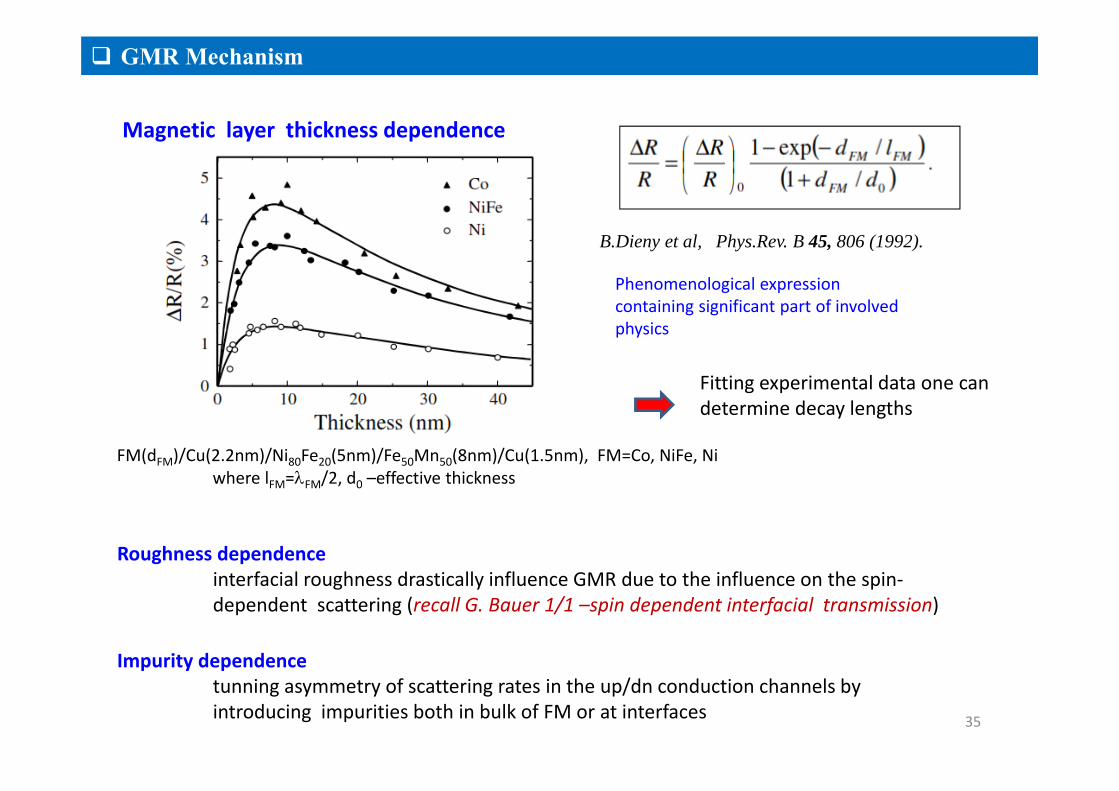
Magnetic layer thickness dependence
B.Dieny et al, Phys.Rev. B 45, 806 (1992).
FM(dFM)/Cu(2.2nm)/Ni80Fe20(5nm)/Fe50Mn50(8nm)/Cu(1.5nm), FM=Co, NiFe, Ni where lFM=FM/2, d0 –effective thickness
Phenomenological expressioncontaining significant part of involvedphysics
Roughness dependence interfacial roughness drastically influence GMR due to the influence on the spin‐dependent scattering (recall G. Bauer 1/1 –spin dependent interfacial transmission)
Impurity dependence tunning asymmetry of scattering rates in the up/dn conduction channels byintroducing impurities both in bulk of FM or at interfaces
GMR Mechanism
35
Fitting experimental data one candetermine decay lengths
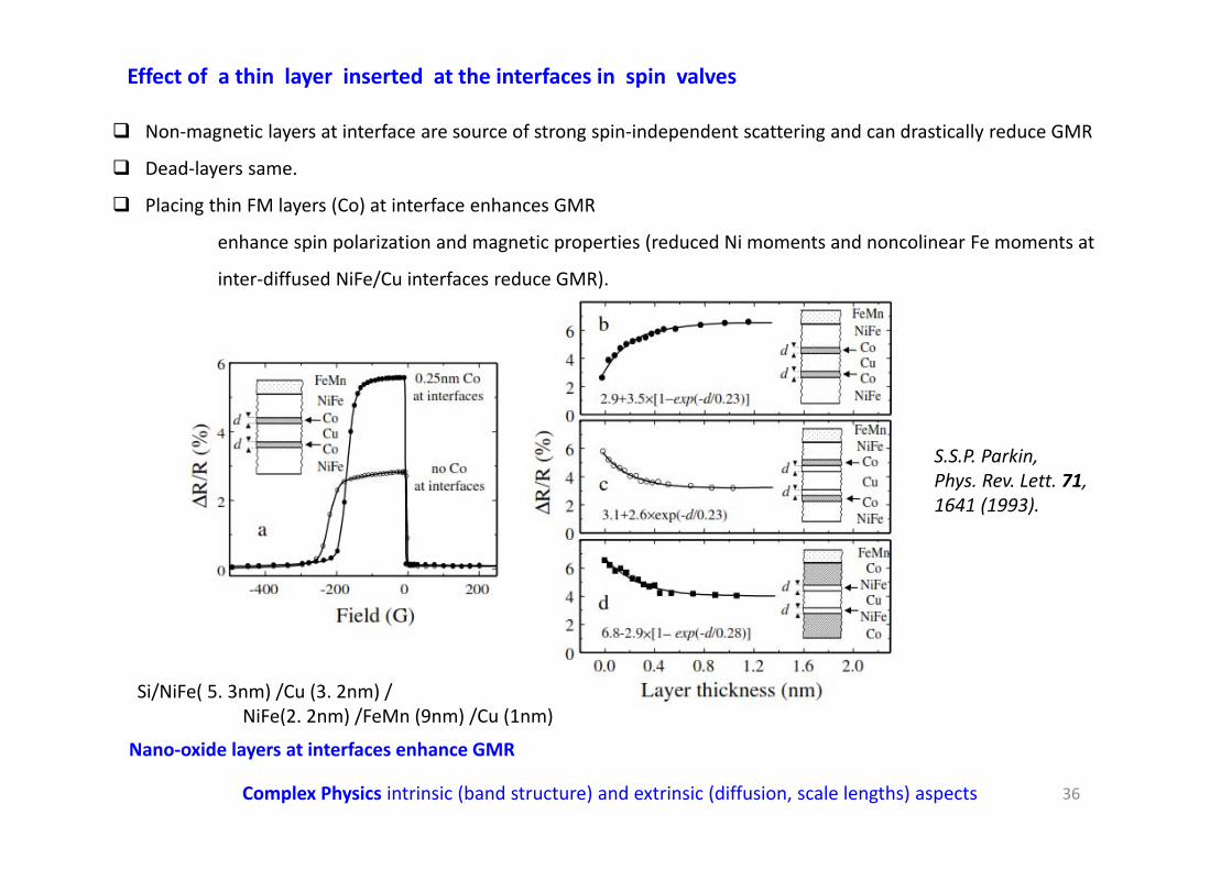
Effect of a thin layer inserted at the interfaces in spin valves
Si/NiFe( 5. 3nm) /Cu (3. 2nm) /NiFe(2. 2nm) /FeMn (9nm) /Cu (1nm)
S.S.P. Parkin, Phys. Rev. Lett. 71, 1641 (1993).
Non‐magnetic layers at interface are source of strong spin‐independent scattering and can drastically reduce GMR
Dead‐layers same.
Placing thin FM layers (Co) at interface enhances GMR
enhance spin polarization and magnetic properties (reduced Ni moments and noncolinear Fe moments at
inter‐diffused NiFe/Cu interfaces reduce GMR).
Nano‐oxide layers at interfaces enhance GMR
Complex Physics intrinsic (band structure) and extrinsic (diffusion, scale lengths) aspects 36
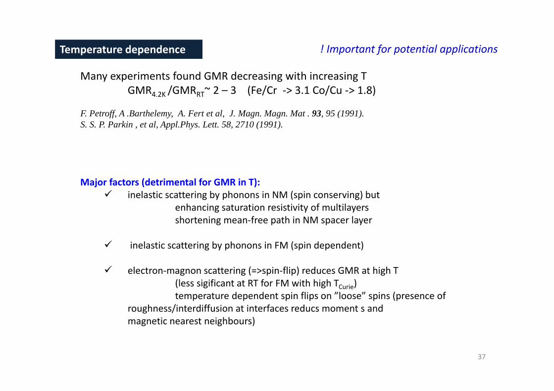
Temperature dependence
Many experiments found GMR decreasing with increasing T GMR4.2K /GMRRT~ 2 – 3 (Fe/Cr ‐> 3.1 Co/Cu ‐> 1.8)
F. Petroff, A .Barthelemy, A. Fert et al, J. Magn. Magn. Mat . 93, 95 (1991).S. S. P. Parkin , et al, Appl.Phys. Lett. 58, 2710 (1991).
Major factors (detrimental for GMR in T): inelastic scattering by phonons in NM (spin conserving) but
enhancing saturation resistivity of multilayersshortening mean‐free path in NM spacer layer
inelastic scattering by phonons in FM (spin dependent)
electron‐magnon scattering (=>spin‐flip) reduces GMR at high T (less sigificant at RT for FM with high TCurie)temperature dependent spin flips on ”loose” spins (presence of
roughness/interdiffusion at interfaces reducs moment s andmagnetic nearest neighbours)
37
! Important for potential applications
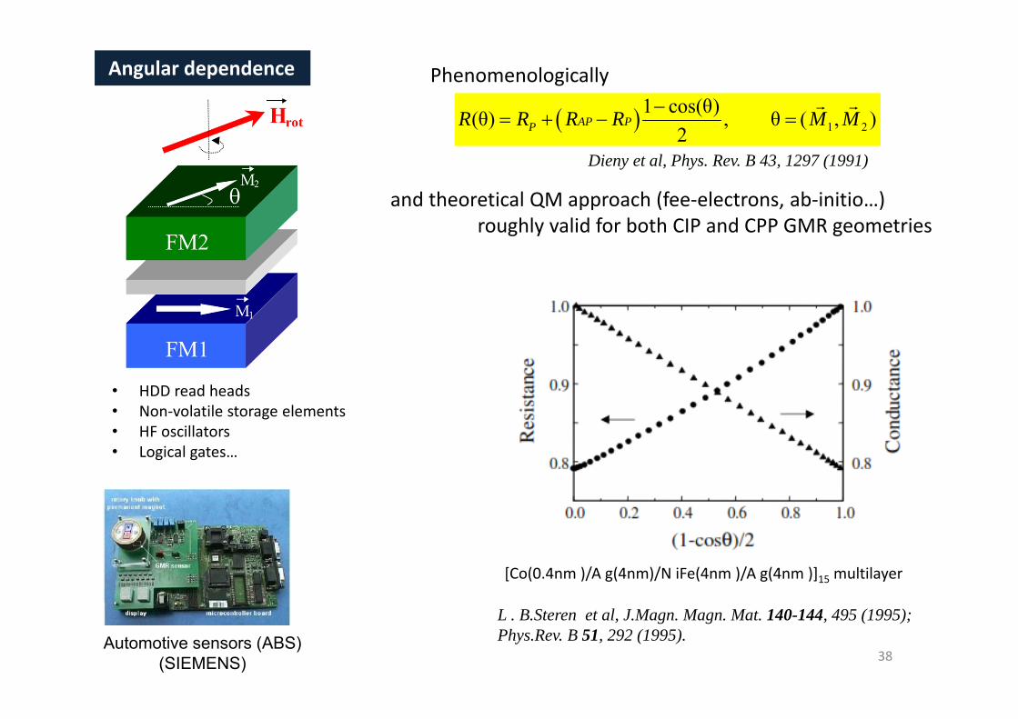
[Co(0.4nm )/A g(4nm)/N iFe(4nm )/A g(4nm )]15 multilayer
L . B.Steren et al, J.Magn. Magn. Mat. 140-144, 495 (1995); Phys.Rev. B 51, 292 (1995).
Angular dependence
1 21 cos(θ)(θ) , θ , )
2AP PPR R R R M M
• HDD read heads• Non‐volatile storage elements• HF oscillators• Logical gates…
Phenomenologically
Dieny et al, Phys. Rev. B 43, 1297 (1991)
and theoretical QM approach (fee‐electrons, ab‐initio…)roughly valid for both CIP and CPP GMR geometries
Automotive sensors (ABS)(SIEMENS) 38
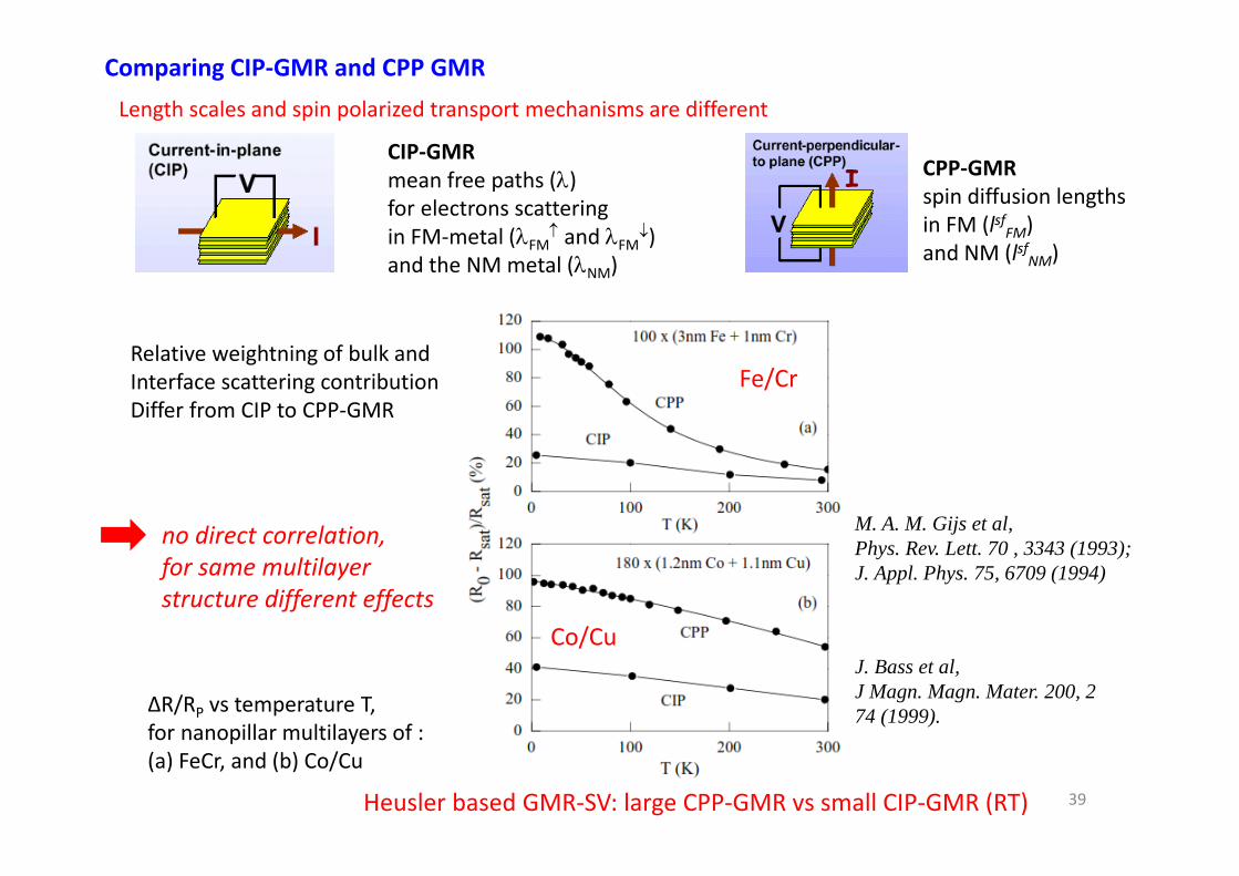
Comparing CIP‐GMR and CPP GMR
CIP‐GMR mean free paths ()for electrons scatteringin FM‐metal (FM and FM) and the NM metal (NM)
CPP‐GMR spin diffusion lengthsin FM (lsfFM)and NM (lsfNM)
Length scales and spin polarized transport mechanisms are different
ΔR/RP vs temperature T, for nanopillar multilayers of : (a) FeCr, and (b) Co/Cu
J. Bass et al,J Magn. Magn. Mater. 200, 274 (1999).
M. A. M. Gijs et al, Phys. Rev. Lett. 70 , 3343 (1993); J. Appl. Phys. 75, 6709 (1994)
Relative weightning of bulk and Interface scattering contributionDiffer from CIP to CPP‐GMR
Heusler based GMR‐SV: large CPP‐GMR vs small CIP‐GMR (RT)
no direct correlation, for same multilayerstructure different effects
Fe/Cr
Co/Cu
39
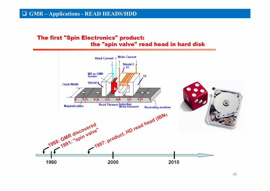
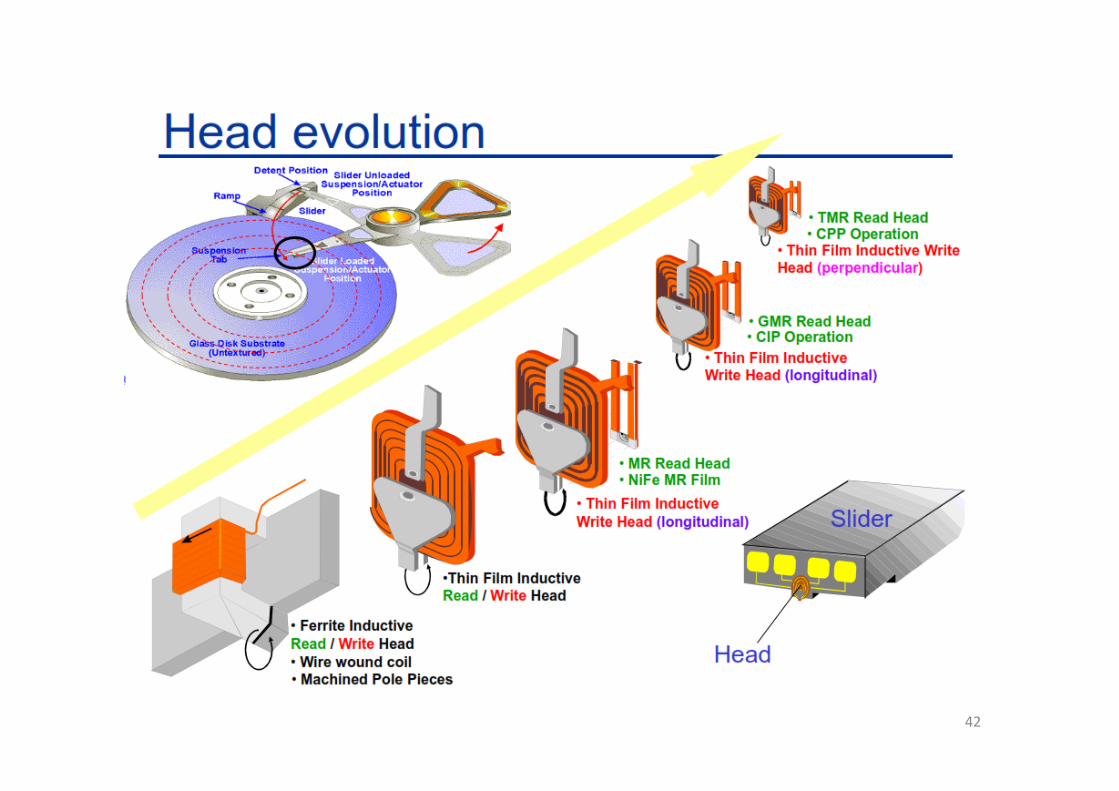
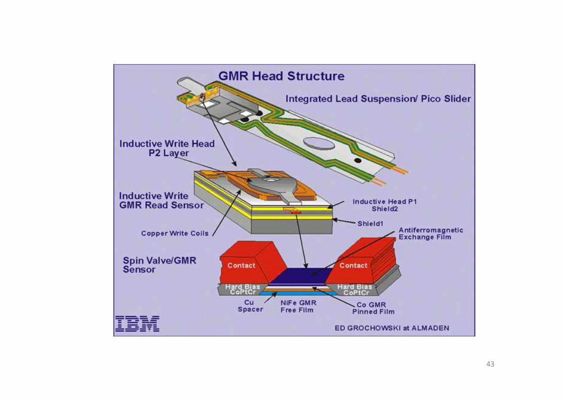
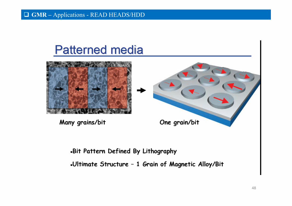
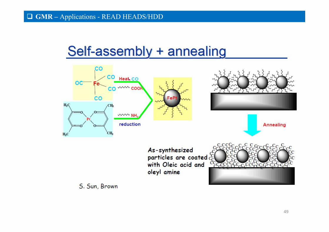
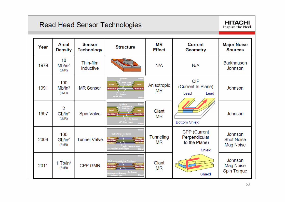
GMR – Applications - READ HEADS/HDD
40
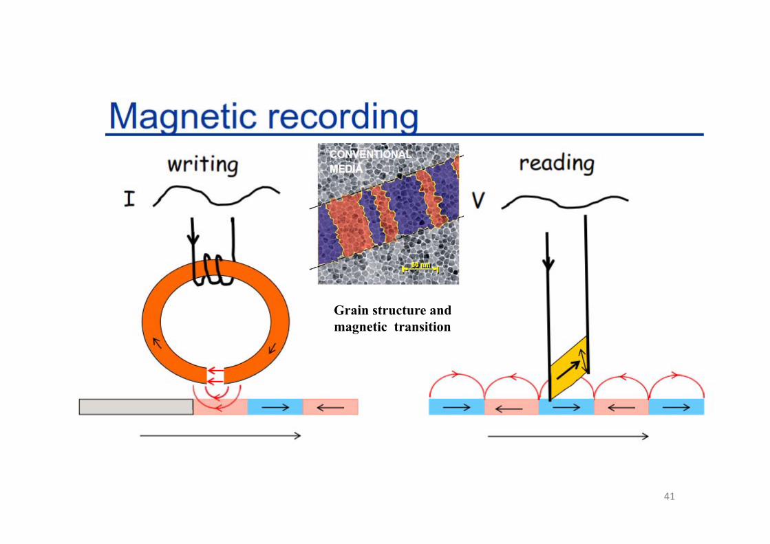
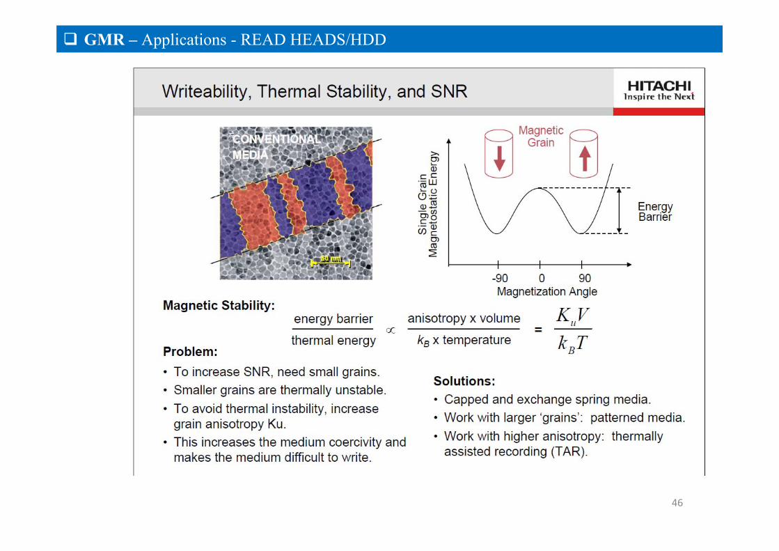
Grain structure and magnetic transition
41
42
43
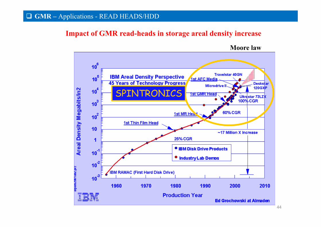
Impact of GMR read-heads in storage areal density increase
SPINTRONICS
Moore law
GMR – Applications - READ HEADS/HDD
44
45
GMR – Applications - READ HEADS/HDD
46
GMR – Applications - READ HEADS/HDD
47
GMR – Applications - READ HEADS/HDD
48
GMR – Applications - READ HEADS/HDD
49
GMR – Applications - READ HEADS/HDD
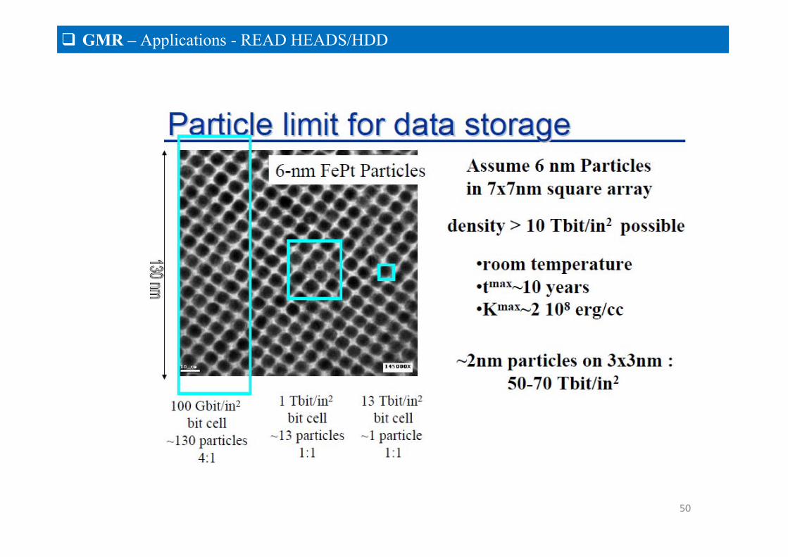
50
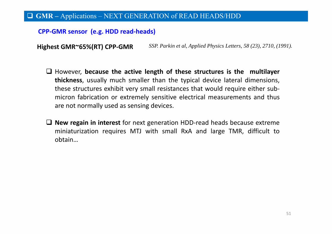
However, because the active length of these structures is the multilayerthickness, usually much smaller than the typical device lateral dimensions,these structures exhibit very small resistances that would require either sub‐micron fabrication or extremely sensitive electrical measurements and thusare not normally used as sensing devices.
New regain in interest for next generation HDD‐read heads because extrememiniaturization requires MTJ with small RxA and large TMR, difficult toobtain…
Highest GMR~65%(RT) CPP‐GMR SSP. Parkin et al, Applied Physics Letters, 58 (23), 2710, (1991).
51
GMR – Applications – NEXT GENERATION of READ HEADS/HDD
CPP‐GMR sensor (e.g. HDD read‐heads)
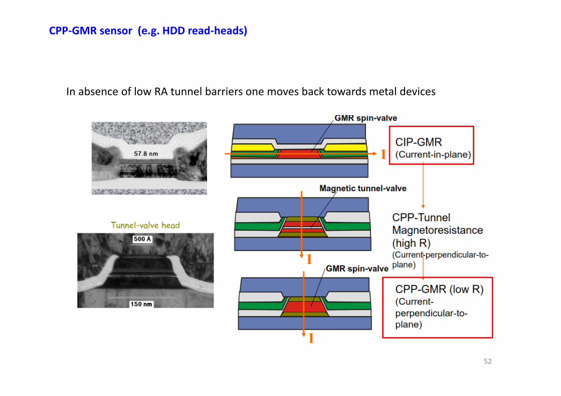
In absence of low RA tunnel barriers one moves back towards metal devices
CPP‐GMR sensor (e.g. HDD read‐heads)
52
53
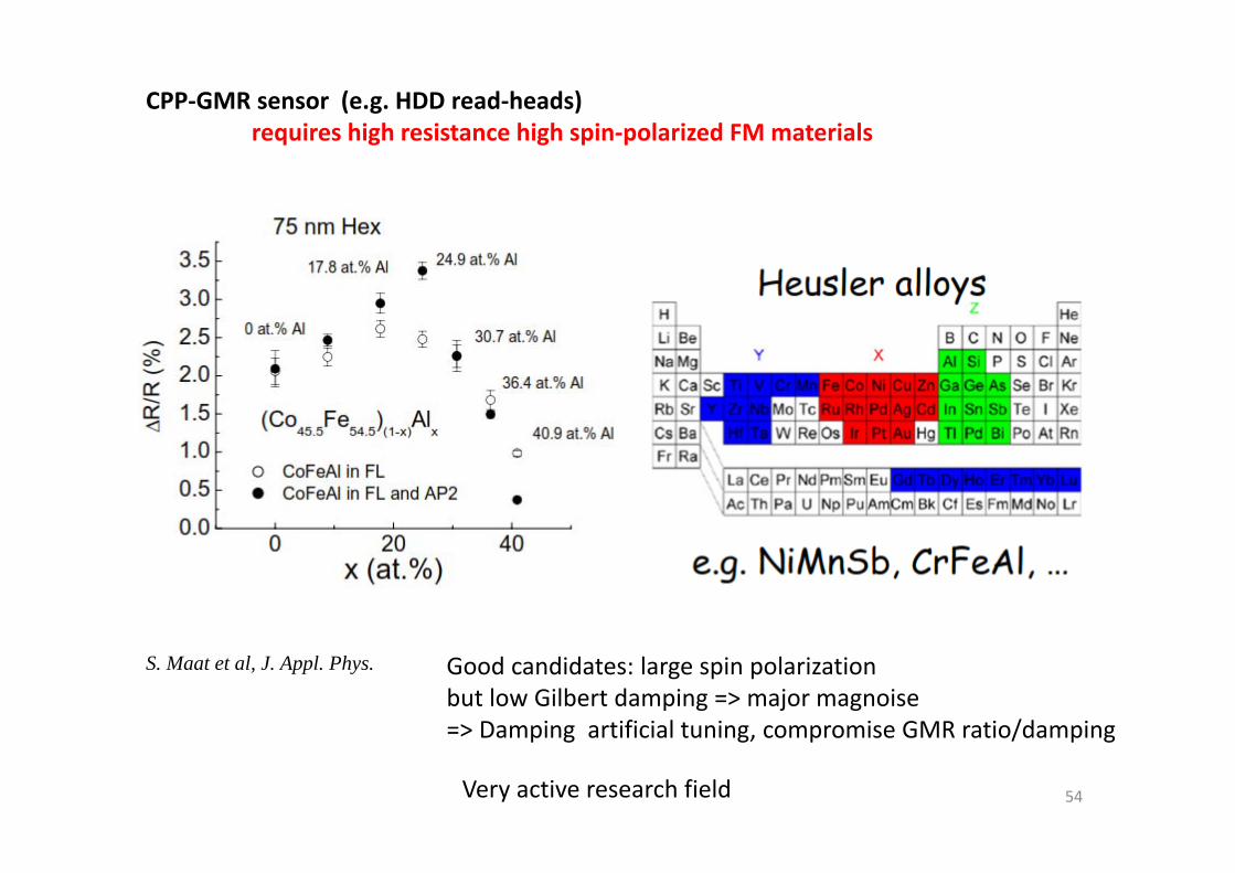
CPP‐GMR sensor (e.g. HDD read‐heads)requires high resistance high spin‐polarized FM materials
S. Maat et al, J. Appl. Phys. Good candidates: large spin polarizationbut low Gilbert damping => major magnoise=> Damping artificial tuning, compromise GMR ratio/damping
Very active research field 54
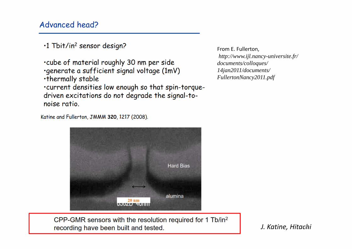
From E. Fullerton, http://www.ijl.nancy-universite.fr/documents/colloques/14jan2011/documents/FullertonNancy2011.pdf
J. Katine, Hitachi55
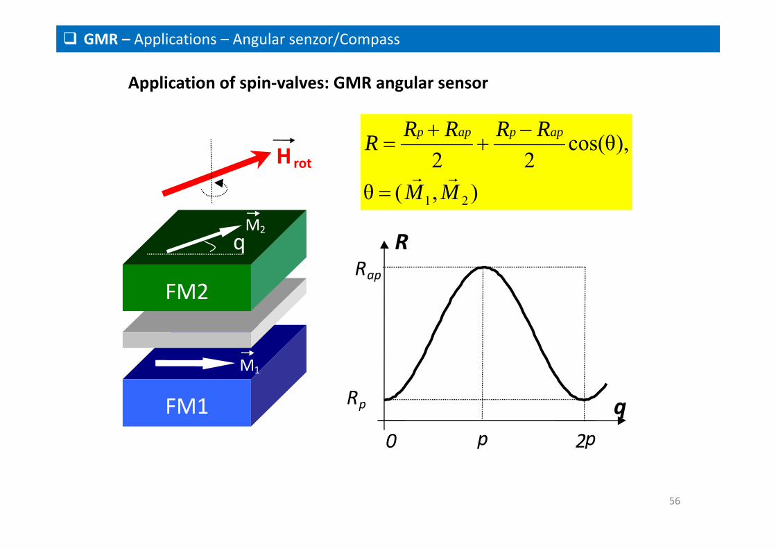
),θ
),θcos(22
21 MM
RRRRR appapp
R
Rp
Rap
q0 p 2p
FM1
FM2
q
M1
M2
Hrot
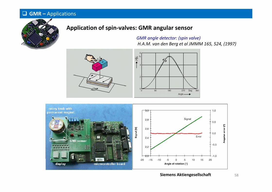
Application of spin‐valves: GMR angular sensor
GMR – Applications – Angular senzor/Compass
56
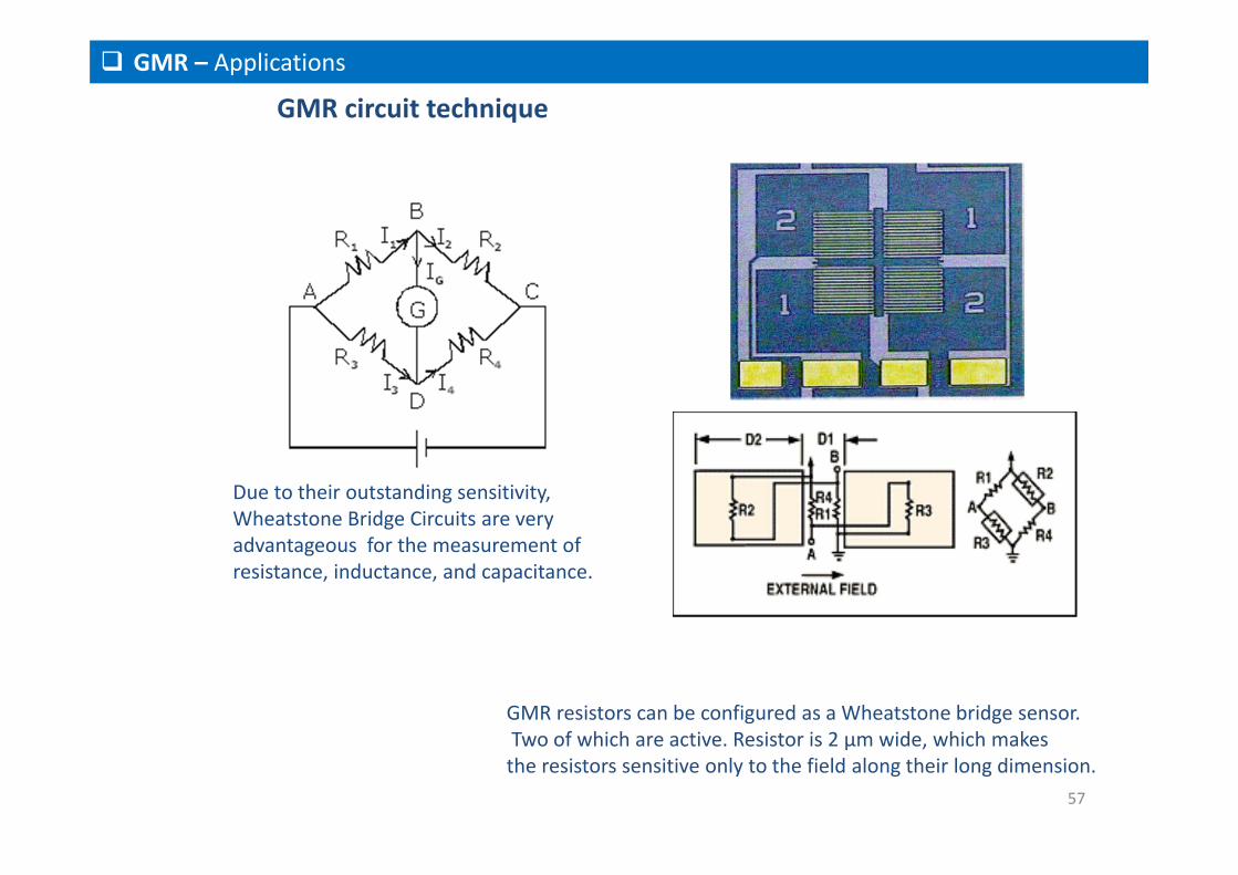
Due to their outstanding sensitivity, Wheatstone Bridge Circuits are very advantageous for the measurement of resistance, inductance, and capacitance.
GMR resistors can be configured as a Wheatstone bridge sensor.Two of which are active. Resistor is 2 µm wide, which makes the resistors sensitive only to the field along their long dimension.
GMR circuit technique
GMR – Applications
57
Siemens Aktiengesellschaft
Application of spin‐valves: GMR angular sensorGMR angle detector: (spin valve)H.A.M. van den Berg et al JMMM 165, 524, (1997)
GMR – Applications
58
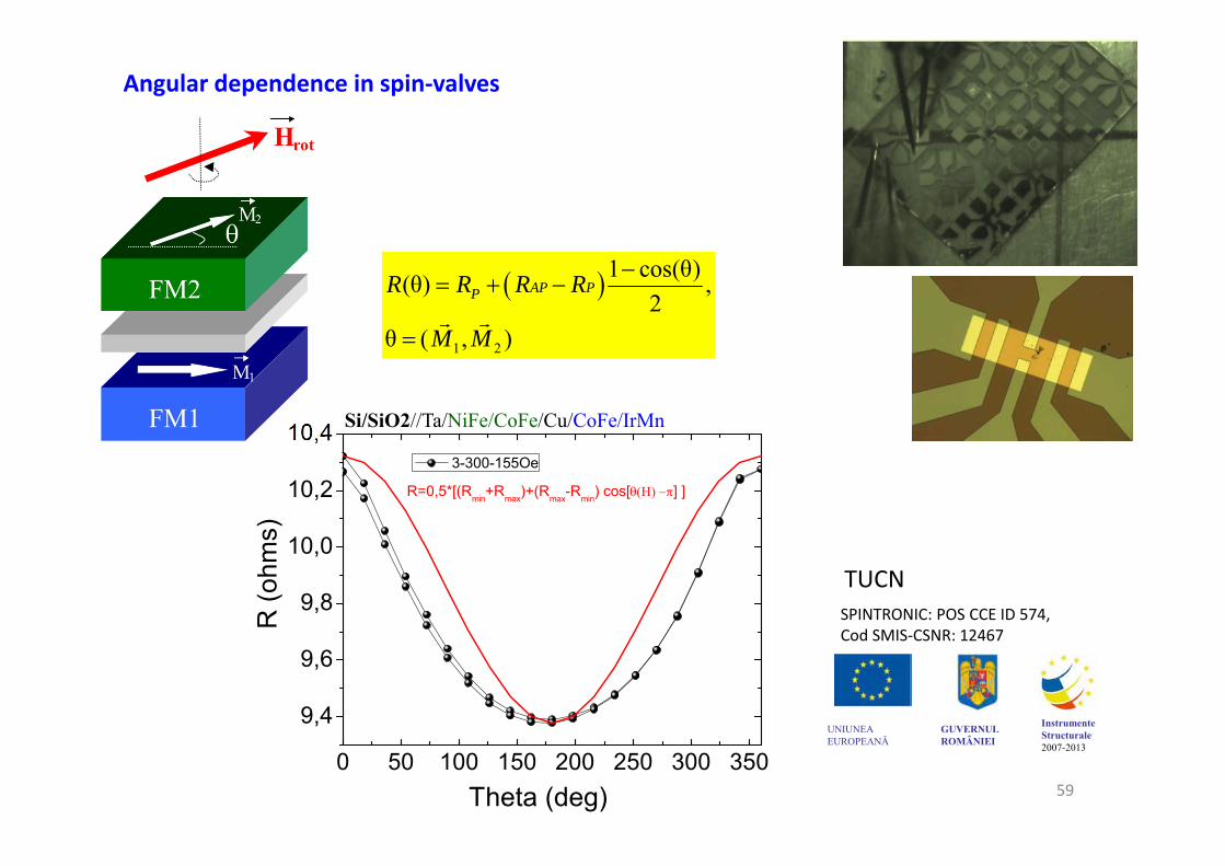
Angular dependence in spin‐valves
0 50 100 150 200 250 300 350
9,4
9,6
9,8
10,0
10,2
10,4
R (o
hms)
Theta (deg)
3-300-155Oe
R=0,5*[(Rmin+Rmax)+(Rmax-Rmin) cos[] ]
1 2
1 cos(θ)(θ) ,2
θ , )
AP PPR R R R
M M
Si/SiO2//Ta/NiFe/CoFe/Cu/CoFe/IrMn
UNIUNEA EUROPEANĂ
GUVERNUL ROMÂNIEI
Instrumente Structurale2007-2013
SPINTRONIC: POS CCE ID 574, Cod SMIS‐CSNR: 12467
TUCN
59
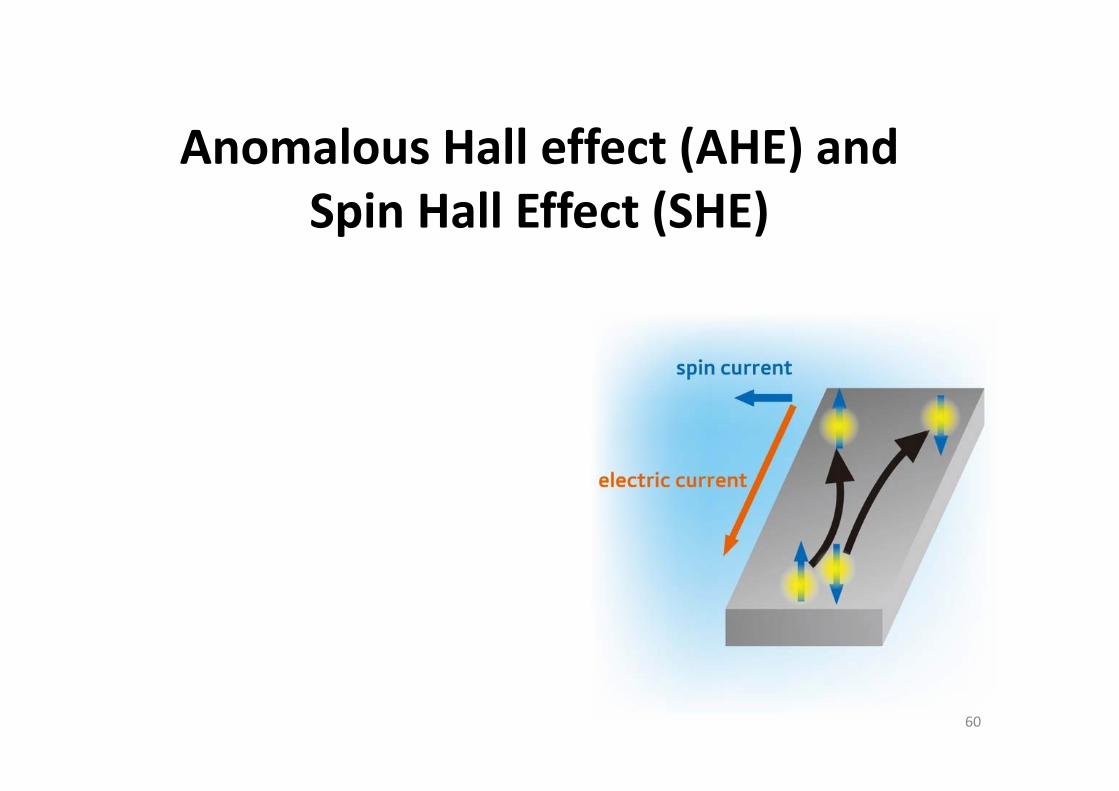
Anomalous Hall effect (AHE) andSpin Hall Effect (SHE)
60
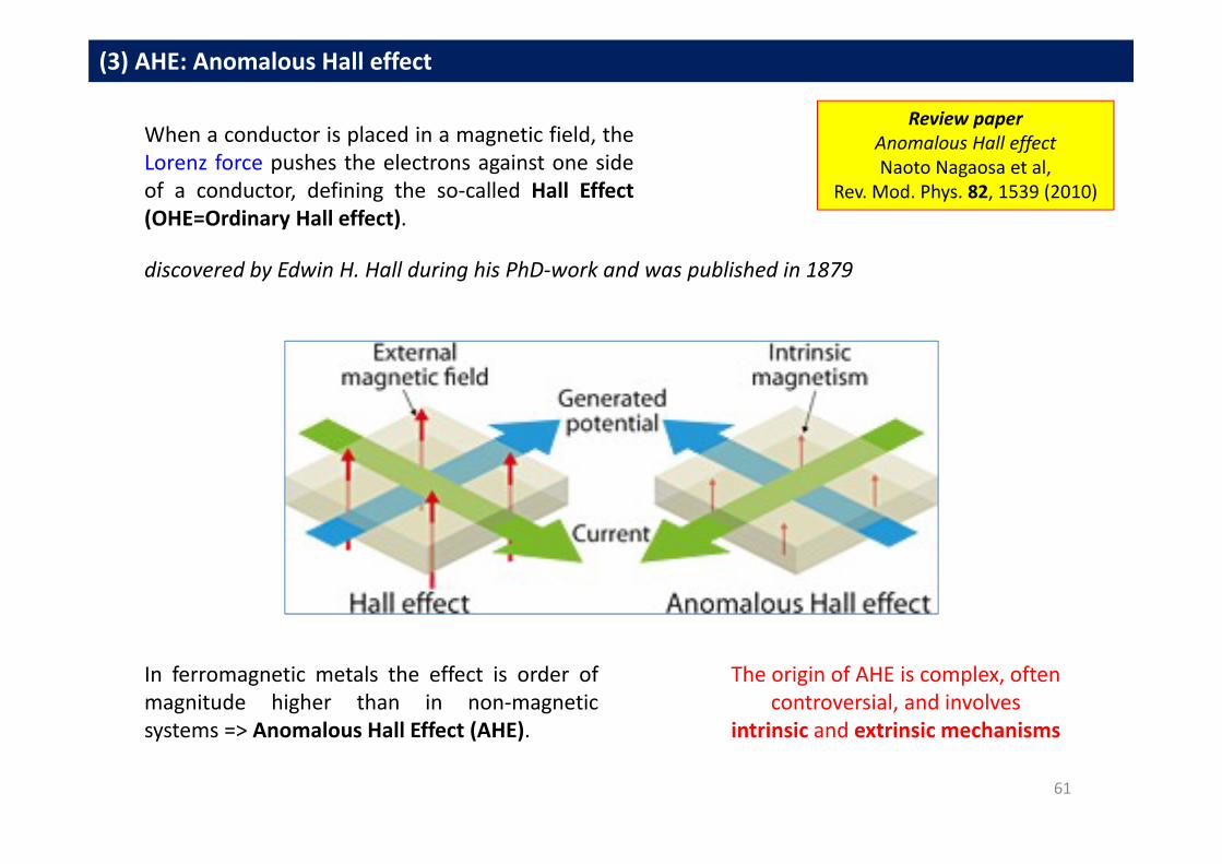
(3) AHE: Anomalous Hall effect
When a conductor is placed in a magnetic field, theLorenz force pushes the electrons against one sideof a conductor, defining the so‐called Hall Effect(OHE=Ordinary Hall effect).
discovered by Edwin H. Hall during his PhD‐work and was published in 1879
In ferromagnetic metals the effect is order ofmagnitude higher than in non‐magneticsystems => Anomalous Hall Effect (AHE).
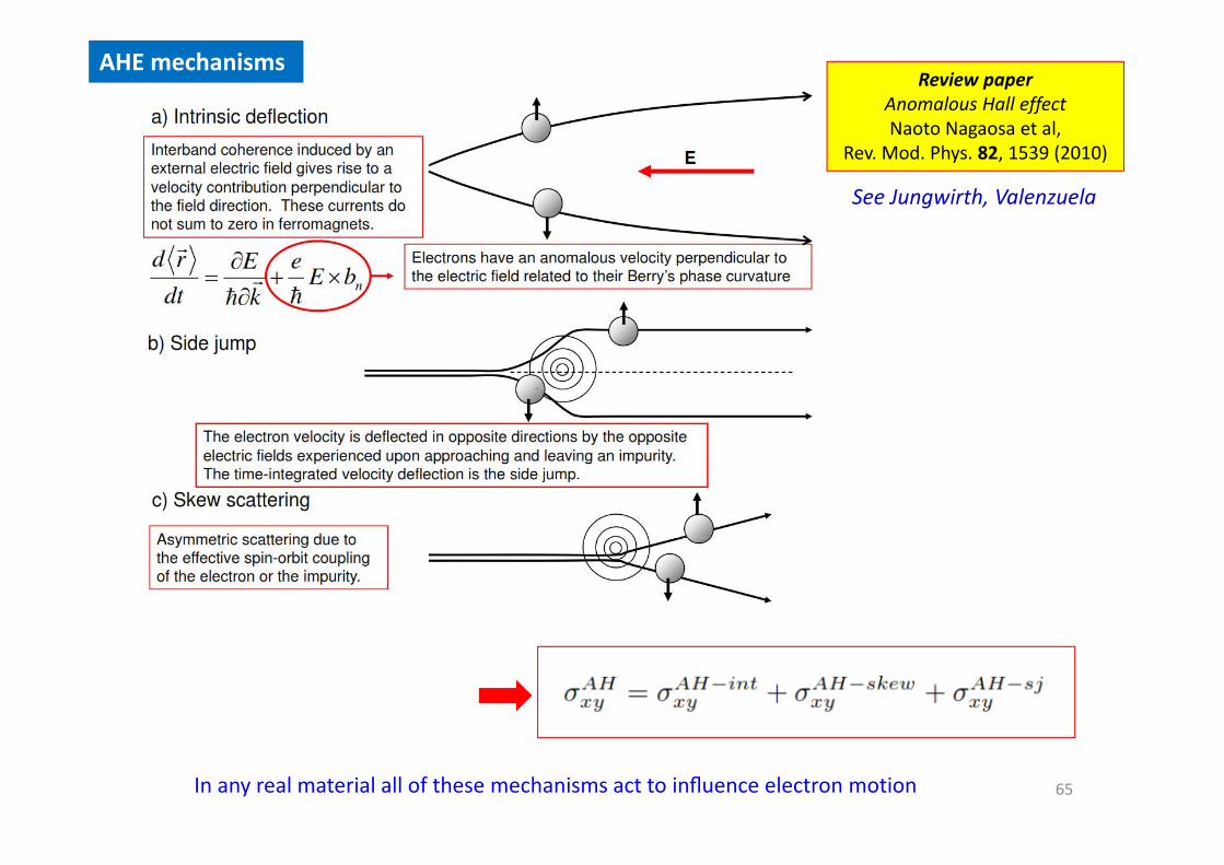
The origin of AHE is complex, often controversial, and involves
intrinsic and extrinsic mechanisms
Review paper Anomalous Hall effectNaoto Nagaosa et al,
Rev. Mod. Phys. 82, 1539 (2010)
61
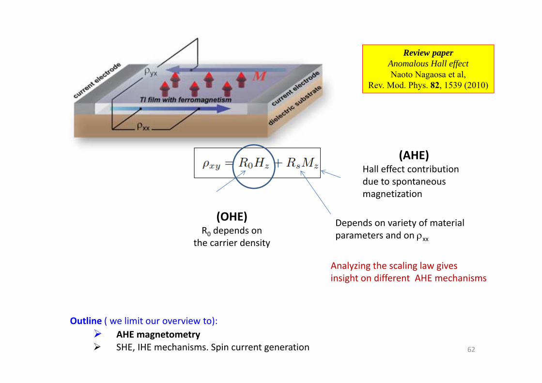
(AHE)Hall effect contribution due to spontaneous magnetization
(OHE)R0 depends on
the carrier density
Depends on variety of material parameters and on xx
Analyzing the scaling law gives insight on different AHE mechanisms
Outline ( we limit our overview to): AHE magnetometry SHE, IHE mechanisms. Spin current generation
Review paper Anomalous Hall effectNaoto Nagaosa et al,
Rev. Mod. Phys. 82, 1539 (2010)
62
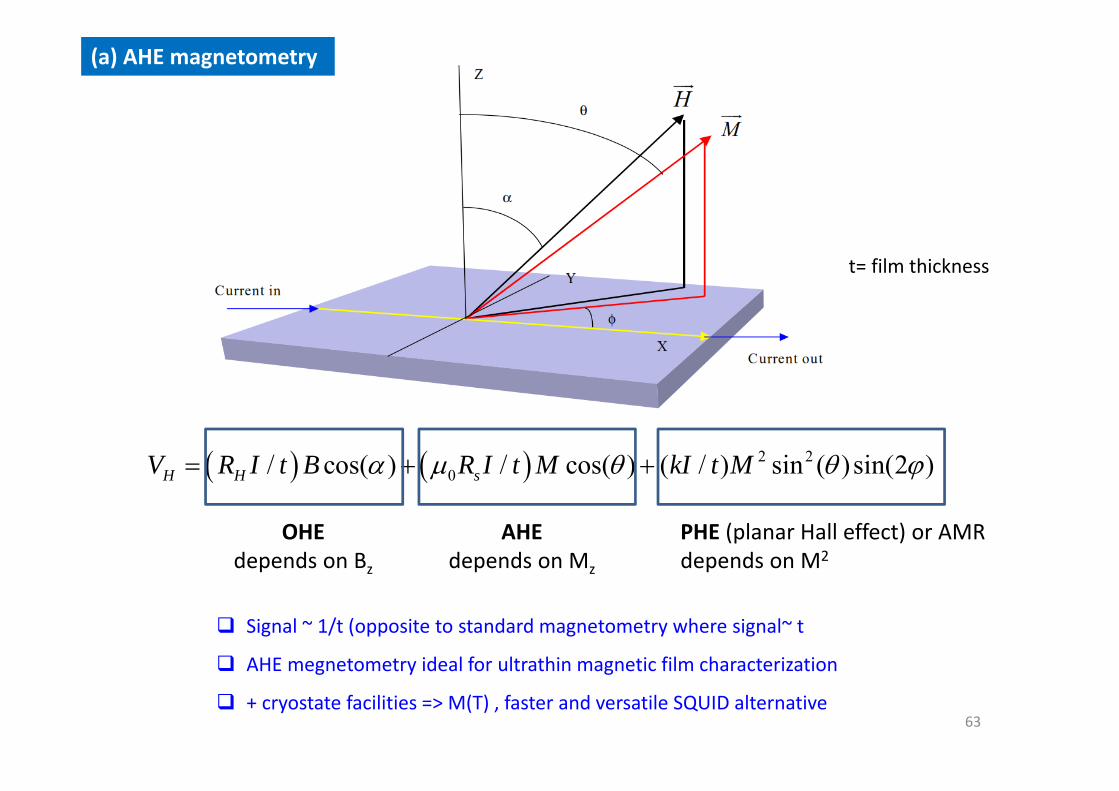
2 20/ cos( ) / cos( ) ( / ) sin ( )sin(2 )H H sV R I t B R I t M kI t M
OHEdepends on Bz
AHEdepends on Mz
PHE (planar Hall effect) or AMRdepends on M2
t= film thickness
Signal ~ 1/t (opposite to standard magnetometry where signal~ t
AHE megnetometry ideal for ultrathin magnetic film characterization
+ cryostate facilities => M(T) , faster and versatile SQUID alternative
(a) AHE magnetometry
63
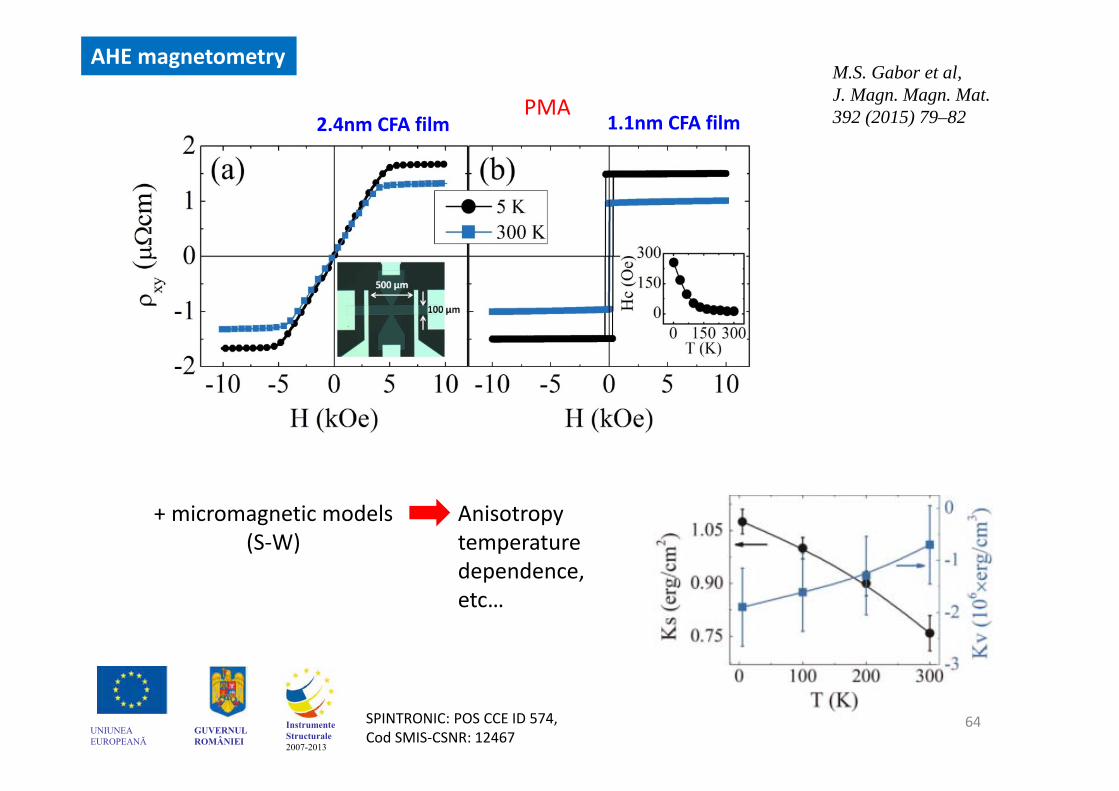
2.4nm CFA film 1.1nm CFA film
M.S. Gabor et al, J. Magn. Magn. Mat.392 (2015) 79–82
AHE magnetometry
UNIUNEA EUROPEANĂ
GUVERNUL ROMÂNIEI
Instrumente Structurale2007-2013
SPINTRONIC: POS CCE ID 574, Cod SMIS‐CSNR: 12467
+ micromagnetic models(S‐W)
Anisotropytemperaturedependence, etc…
PMA
64
AHE mechanisms
In any real material all of these mechanisms act to influence electron motion 65
Review paper Anomalous Hall effectNaoto Nagaosa et al,
Rev. Mod. Phys. 82, 1539 (2010)
See Jungwirth, Valenzuela
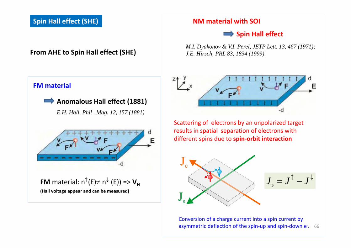
Anomalous Hall effect (1881)
Spin Hall effect
E.H. Hall, Phil . Mag. 12, 157 (1881)
M.I. Dyakonov & V.I. Perel, JETP Lett. 13, 467 (1971); J.E. Hirsch, PRL 83, 1834 (1999)
Scattering of electrons by an unpolarized target results in spatial separation of electrons with different spins due to spin‐orbit interaction
From AHE to Spin Hall effect (SHE)
Conversion of a charge current into a spin current by asymmetric deflection of the spin‐up and spin‐down e‐.
FMmaterial: n(E) n (E)) => VH(Hall voltage appear and can be measured)
NM material with SOI
FM material
sJ J J
Spin Hall effect (SHE)
66
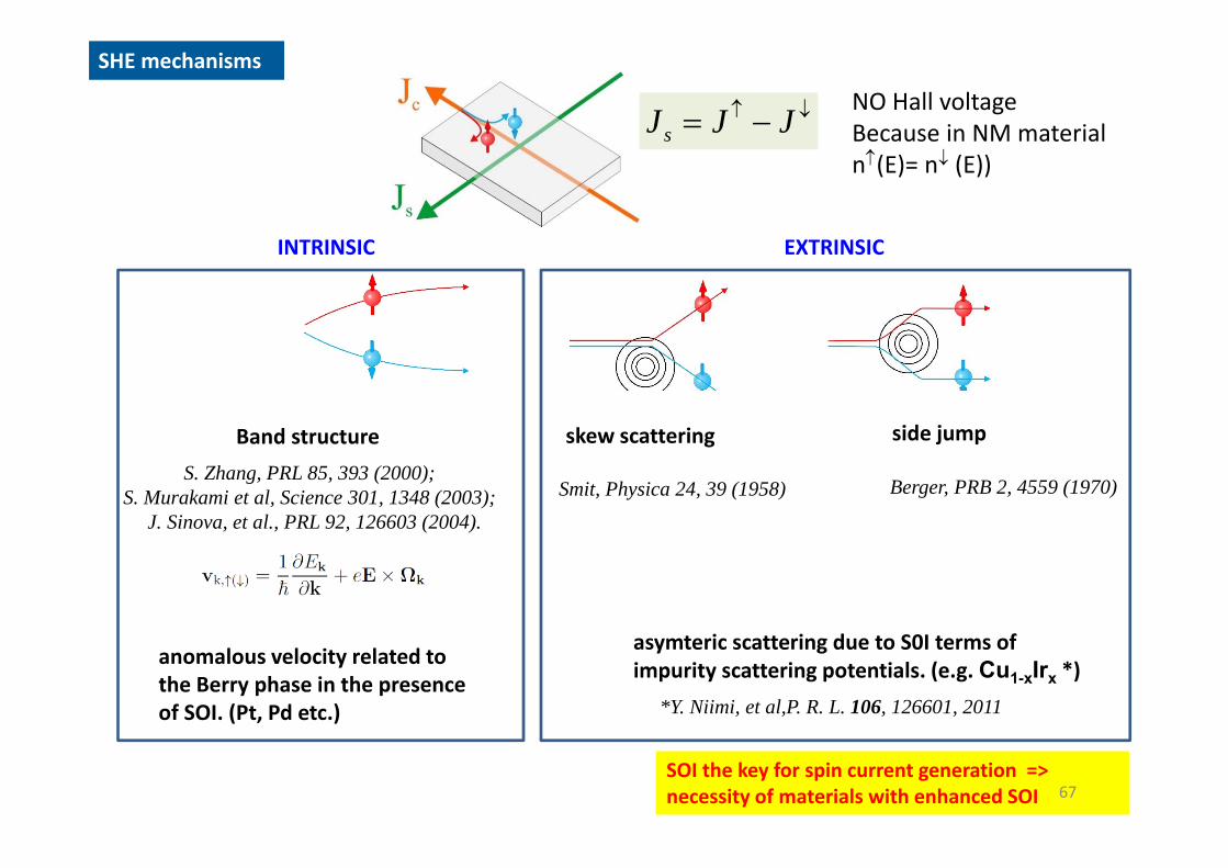
SHE mechanisms
INTRINSIC EXTRINSIC
skew scattering side jump
SOI the key for spin current generation => necessity of materials with enhanced SOI
*Y. Niimi, et al,P. R. L. 106, 126601, 2011
Smit, Physica 24, 39 (1958) Berger, PRB 2, 4559 (1970)S. Zhang, PRL 85, 393 (2000);
S. Murakami et al, Science 301, 1348 (2003);J. Sinova, et al., PRL 92, 126603 (2004).
Band structure
anomalous velocity related to the Berry phase in the presence of SOI. (Pt, Pd etc.)
asymteric scattering due to S0I terms of impurity scattering potentials. (e.g. Cu1-xIrx *)
sJ J J
67
NO Hall voltageBecause in NM materialn(E)= n (E))
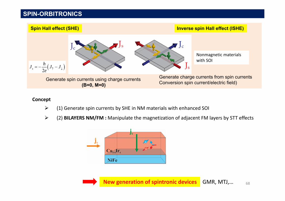
Spin Hall effect (SHE) Inverse spin Hall effect (ISHE)
Nonmagnetic materialswith SOI
Generate spin currents using charge currents(B=0, M=0)
Generate charge currents from spin currentsConversion spin current/electric field)
2shJ J Je
Concept
(1) Generate spin currents by SHE in NM materials with enhanced SOI
(2) BILAYERS NM/FM : Manipulate the magnetization of adjacent FM layers by STT effects
SPIN-ORBITRONICS
New generation of spintronic devices GMR, MTJ,… 68
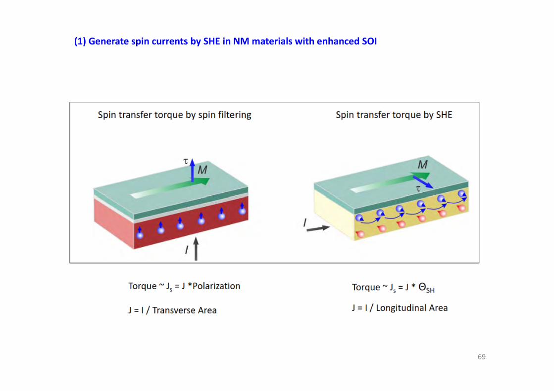
(1) Generate spin currents by SHE in NM materials with enhanced SOI
69
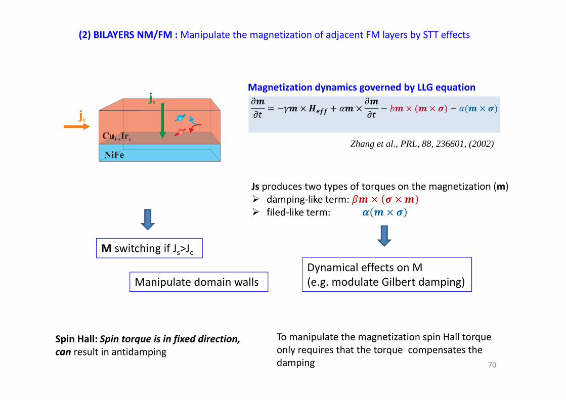
Js produces two types of torques on the magnetization (m) damping‐like term: filed‐like term:
Zhang et al., PRL, 88, 236601, (2002)
Magnetization dynamics governed by LLG equation
M switching if Js>JcDynamical effects on M(e.g. modulate Gilbert damping)Manipulate domain walls
Spin Hall: Spin torque is in fixed direction,can result in antidamping
To manipulate the magnetization spin Hall torqueonly requires that the torque compensates thedamping
(2) BILAYERS NM/FM : Manipulate the magnetization of adjacent FM layers by STT effects
70
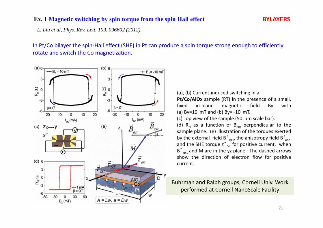
In Pt/Co bilayer the spin‐Hall effect (SHE) in Pt can produce a spin torque strong enough to efficiently rotate and switch the Co magnetization.
Ex. 1 Magnetic switching by spin torque from the spin Hall effect
(a), (b) Current‐induced switching in aPt/Co/AlOx sample (RT) in the presence of a small,fixed in‐plane magnetic field By with(a) By=10 mT and (b) By=−10 mT.(c) Top view of the sample (50 μm scale bar).(d) RH as a function of Bext perpendicular to thesample plane. (e) Illustration of the torques exertedby the external field B ext, the anisotropy field B an,and the SHE torque τ ST for positive current, whenB ext and M are in the yz plane. The dashed arrowsshow the direction of electron flow for positivecurrent.
BYLAYERSL. Liu et al, Phys. Rev. Lett. 109, 096602 (2012)
Buhrman and Ralph groups, Cornell Univ. Work performed at Cornell NanoScale Facility
71
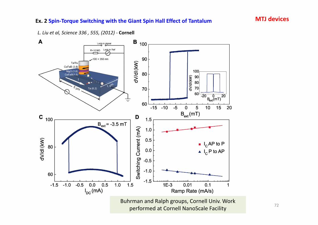
Ex. 2 Spin‐Torque Switching with the Giant Spin Hall Effect of Tantalum
L. Liu et al, Science 336 , 555, (2012) ‐ Cornell
MTJ devices
Buhrman and Ralph groups, Cornell Univ. Work performed at Cornell NanoScale Facility 72
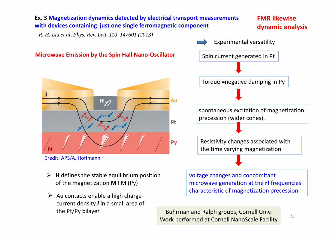
H defines the stable equilibrium position of the magnetization M FM (Py)
Au contacts enable a high charge‐current density I in a small area of the Pt/Py bilayer
Spin current generated in Pt
Torque =negative damping in Py
spontaneous excitation of magnetization precession (wider cones).
Credit: APS/A. Hoffmann
Resistivity changes associated with the time varying magnetization
voltage changes and concomitant microwave generation at the rf frequencies characteristic of magnetization precession
Microwave Emission by the Spin Hall Nano‐Oscillator
R. H. Liu et al, Phys. Rev. Lett. 110, 147601 (2013)
Ex. 3 Magnetization dynamics detected by electrical transport measurements with devices containing just one single ferromagnetic component
Experimental versatility
Buhrman and Ralph groups, Cornell Univ. Work performed at Cornell NanoScale Facility
FMR likewisedynamic analysis
73
Ex. 4 Spin Hall effect tunnelling spectroscopy
L. Liu et al, Nature Physics 10, 561–566 (2014) doi:10.1038/nphys3004
The spin Hall effect (SHE) and ISHE have been widely used to generate and detect spin currents
SHE, which originates from the spin–orbit interaction, is expected to be energy dependent
By tunnelling spectroscopy technique developed to measure the SHE under finite bias voltages.
The SHE has been studied for typical 5dtransition metals. At zero d.c. bias, the obtained spin Hall angles confirm the results from spin‐torque experiments.
At high bias, the transverse spin Hall signals of these materials exhibit very different voltage dependences. The SHE tunnelling spectra have important implications in pinpointing the mechanisms of the SHE and provide guidelines for engineering high‐SHE materials. Moreover, SHE tunnelling spectroscopy can be directly applied to two‐dimensional surface states with strong spin–orbit coupling, such as Dirac electrons in topological insulators.
J. Z. Sun group IBM Watson
Deeper and deeperanalysis…
74
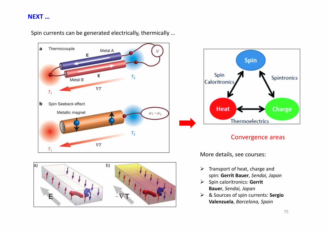
Spin currents can be generated electrically, thermically …
Convergence areas
NEXT …
More details, see courses:
Transport of heat, charge and spin: Gerrit Bauer, Sendai, Japan
Spin caloritronics: Gerrit Bauer, Sendai, Japan
& Sources of spin currents: Sergio Valenzuela, Barcelona, Spain
75
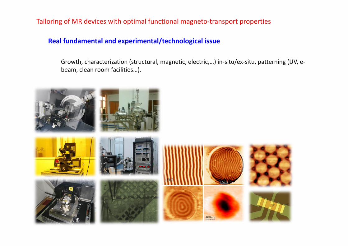
Tailoring of MR devices with optimal functional magneto‐transport properties
Real fundamental and experimental/technological issue
Growth, characterization (structural, magnetic, electric,…) in‐situ/ex‐situ, patterning (UV, e‐beam, clean room facilities…).
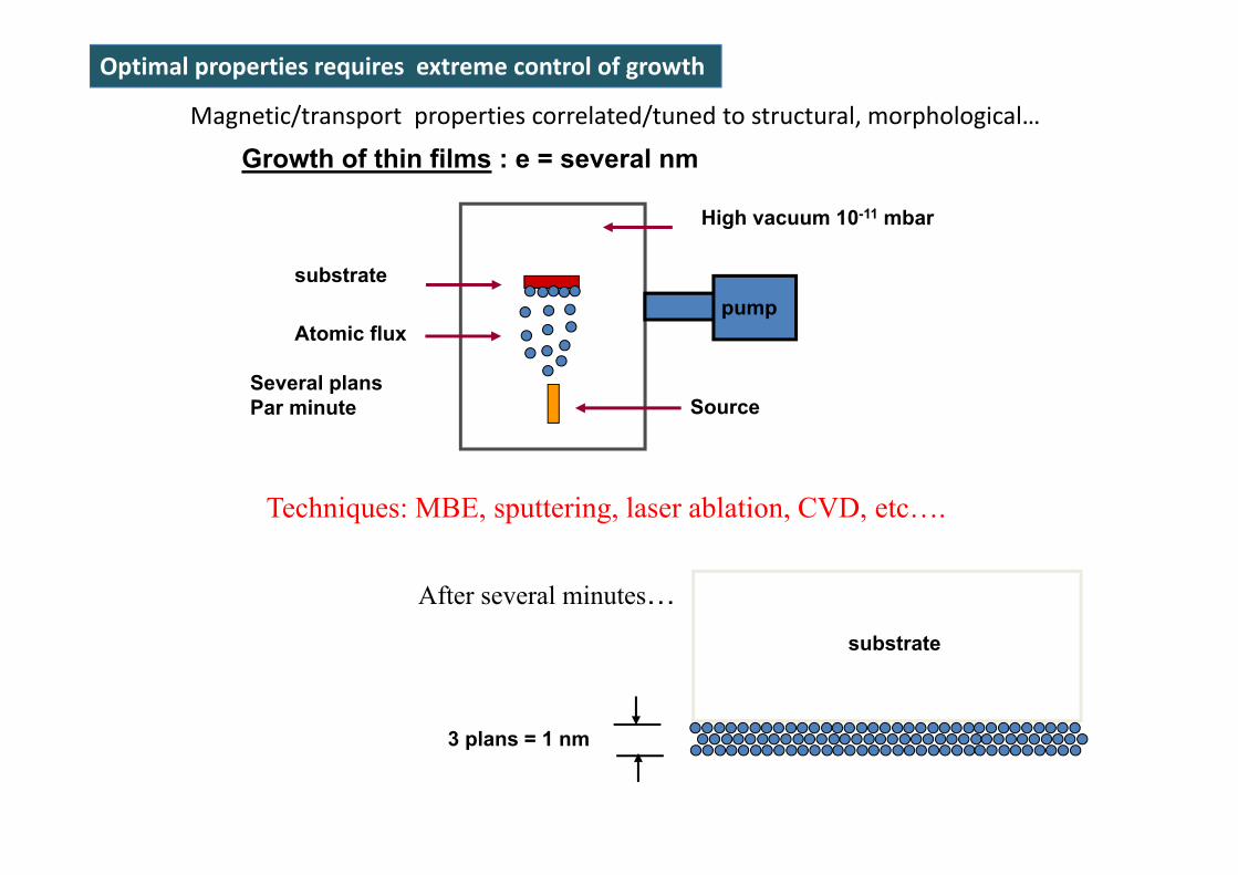
Growth of thin films : e = several nm
High vacuum 10-11 mbar
Source
Atomic flux
Several plansPar minute
substratepump
3 plans = 1 nm
substrate
After several minutes…
Techniques: MBE, sputtering, laser ablation, CVD, etc….
Optimal properties requires extreme control of growth
Magnetic/transport properties correlated/tuned to structural, morphological…
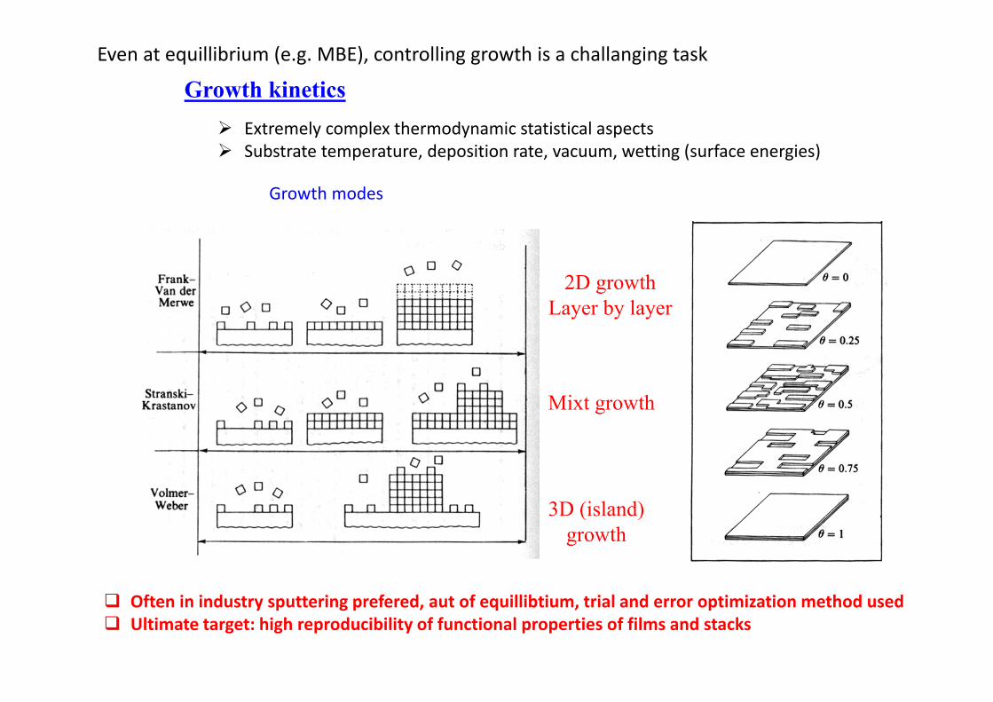
Growth kinetics Extremely complex thermodynamic statistical aspects Substrate temperature, deposition rate, vacuum, wetting (surface energies)
2D growthLayer by layer
Mixt growth
3D (island)growth
Growth modes
Even at equillibrium (e.g. MBE), controlling growth is a challanging task
Often in industry sputtering prefered, aut of equillibtium, trial and error optimization method used Ultimate target: high reproducibility of functional properties of films and stacks
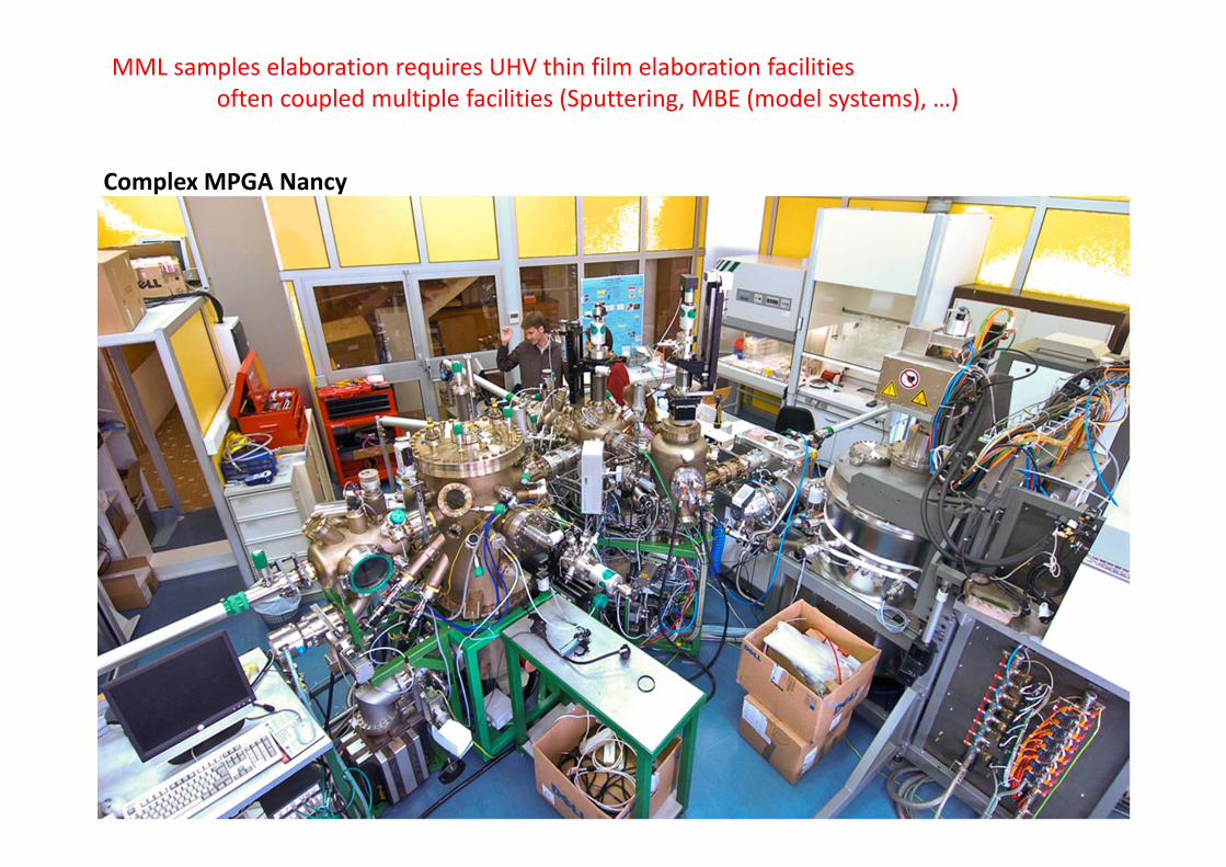
Complex MPGA Nancy
MML samples elaboration requires UHV thin film elaboration facilities often coupled multiple facilities (Sputtering, MBE (model systems), …)
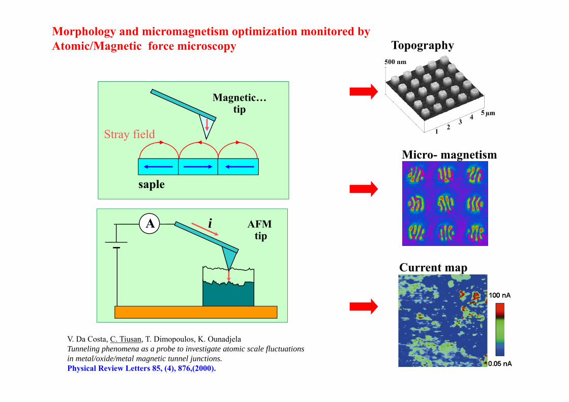
Current map
i AFM tip
A
Topography
Micro- magnetism
Morphology and micromagnetism optimization monitored byAtomic/Magnetic force microscopy
Magnetic…tip
saple
Stray field
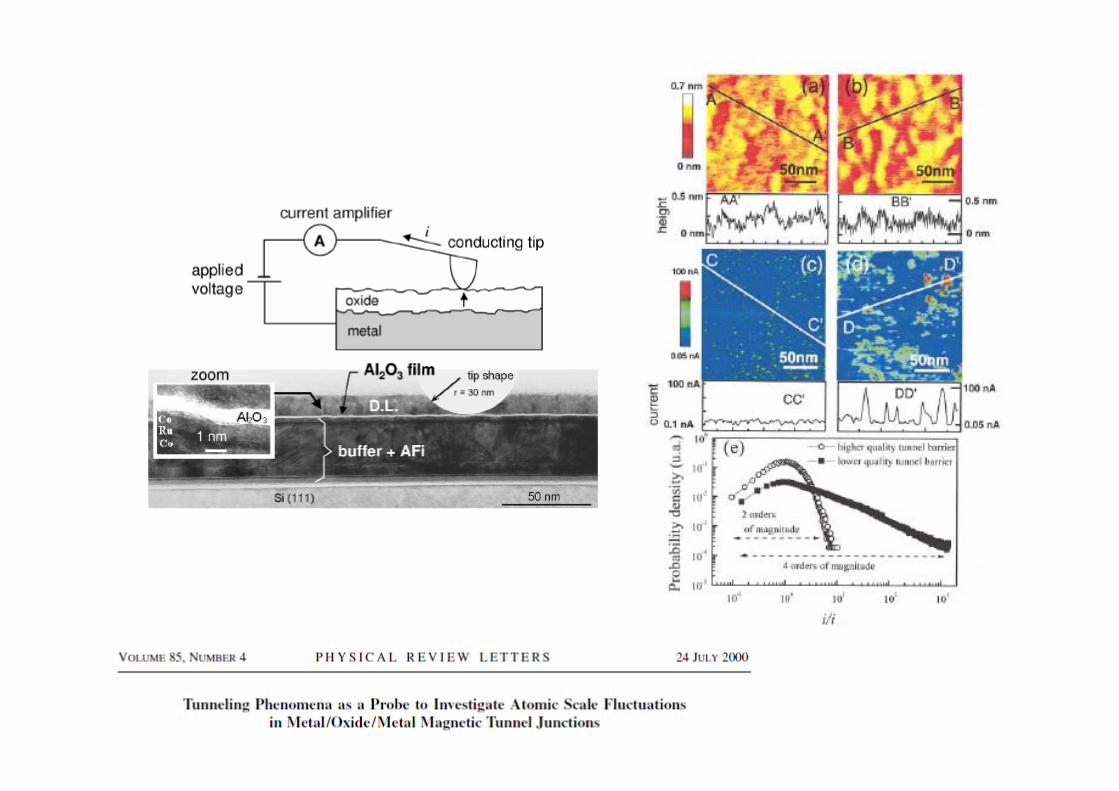
V. Da Costa, C. Tiusan, T. Dimopoulos, K. OunadjelaTunneling phenomena as a probe to investigate atomic scale fluctuations in metal/oxide/metal magnetic tunnel junctions.Physical Review Letters 85, (4), 876,(2000).
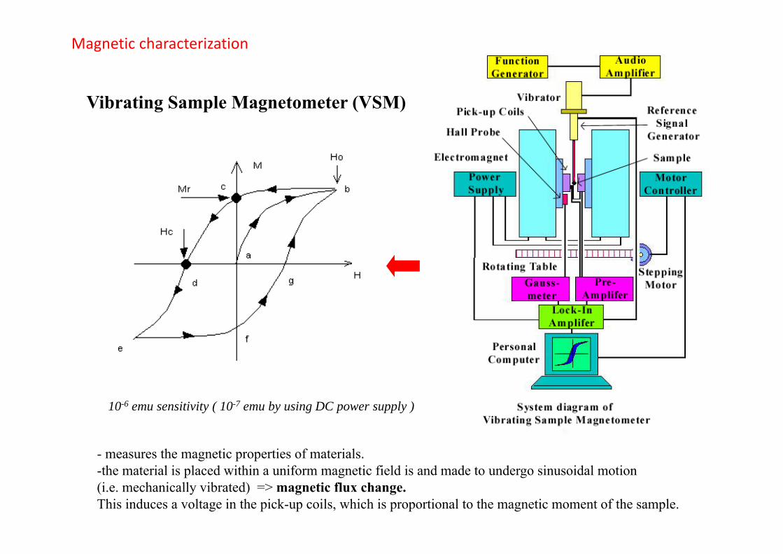
- measures the magnetic properties of materials. -the material is placed within a uniform magnetic field is and made to undergo sinusoidal motion (i.e. mechanically vibrated) => magnetic flux change. This induces a voltage in the pick-up coils, which is proportional to the magnetic moment of the sample.
Vibrating Sample Magnetometer (VSM)
10-6 emu sensitivity ( 10-7 emu by using DC power supply )
Magnetic characterization
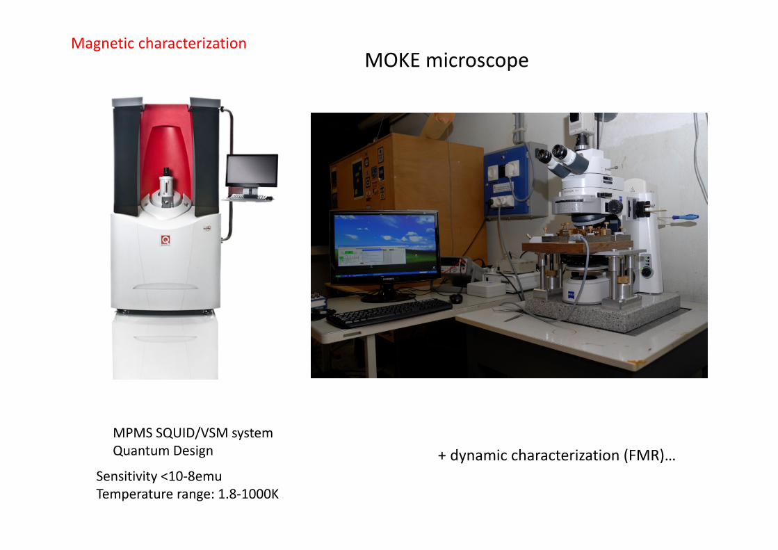
MPMS SQUID/VSM systemQuantum Design
Sensitivity <10‐8emuTemperature range: 1.8‐1000K
Magnetic characterizationMOKE microscope
+ dynamic characterization (FMR)…
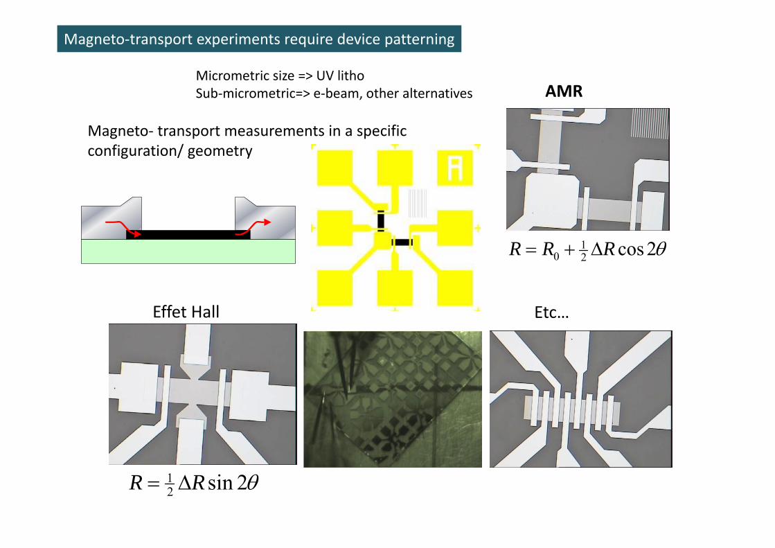
2cos21
0 RRR
AMR
Effet Hall
2sin21 RR
Etc…
Magneto‐ transport measurements in a specificconfiguration/ geometry
Magneto‐transport experiments require device patterning
Micrometric size => UV lithoSub‐micrometric=> e‐beam, other alternatives
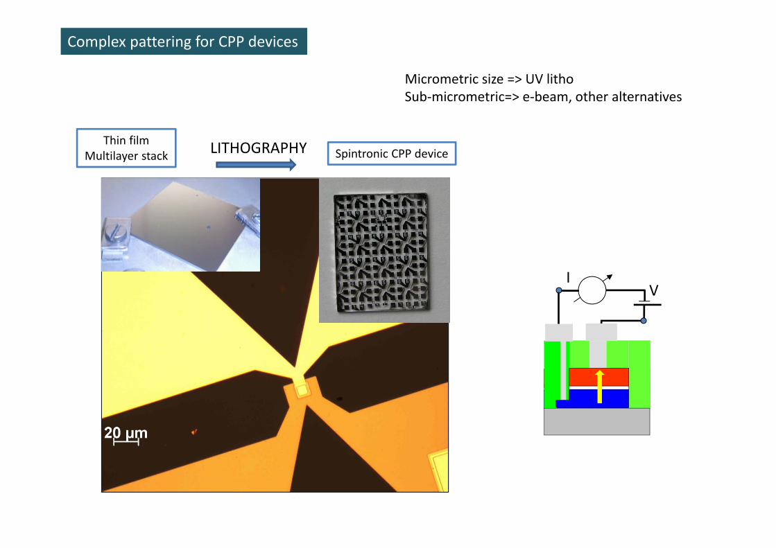
Thin filmMultilayer stack Spintronic CPP deviceLITHOGRAPHY
IV
Complex pattering for CPP devices
Micrometric size => UV lithoSub‐micrometric=> e‐beam, other alternatives
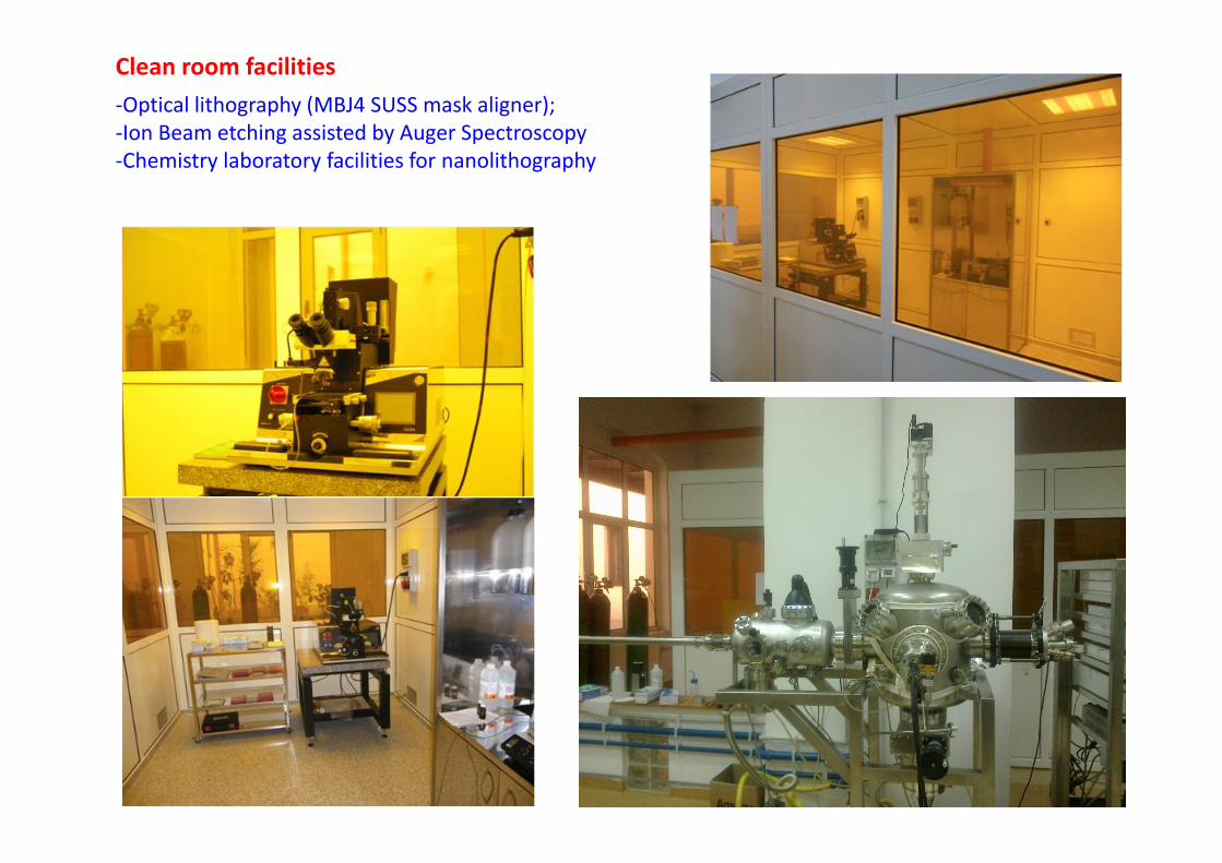
Clean room facilities ‐Optical lithography (MBJ4 SUSS mask aligner); ‐Ion Beam etching assisted by Auger Spectroscopy‐Chemistry laboratory facilities for nanolithography
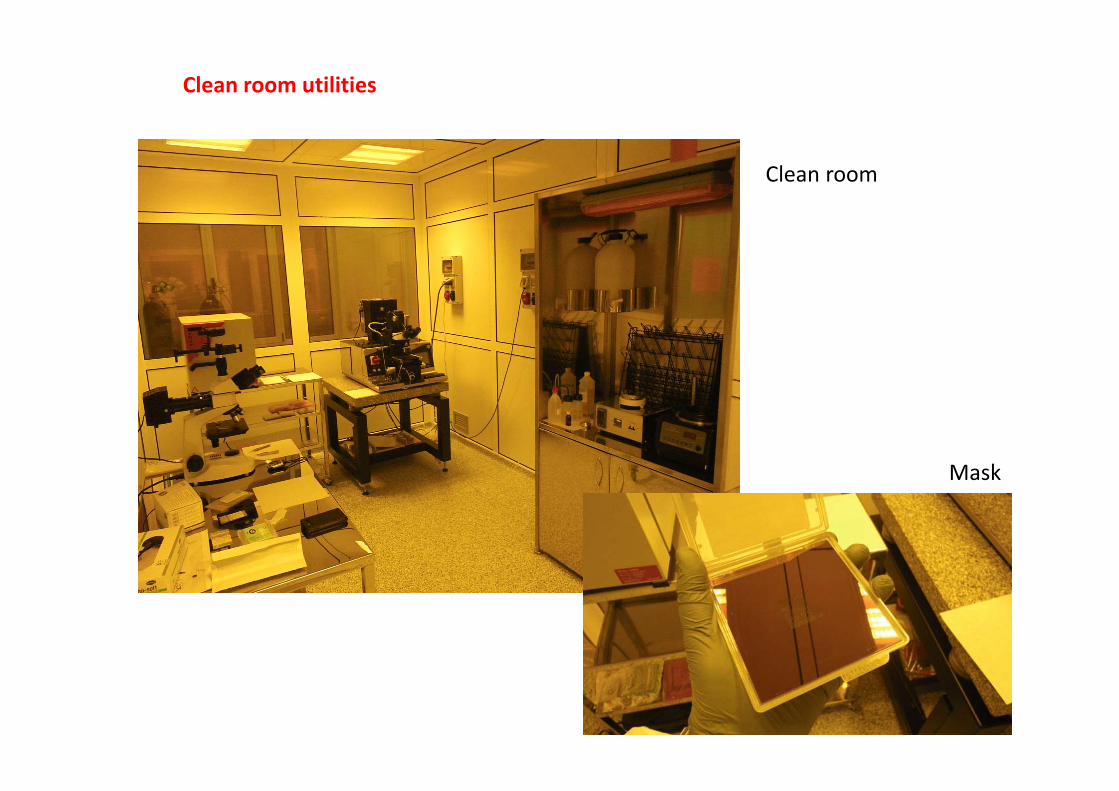
Clean room
Mask
Clean room utilities
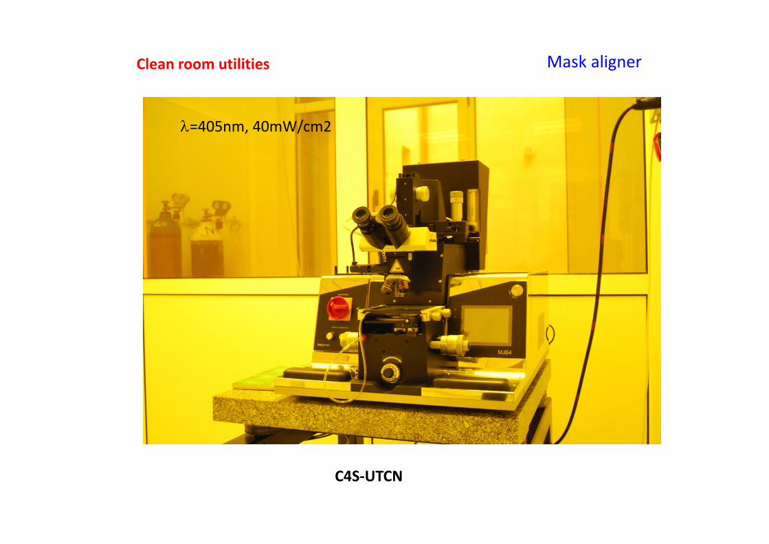
C4S‐UTCN
=405nm, 40mW/cm2
Clean room utilities Mask aligner
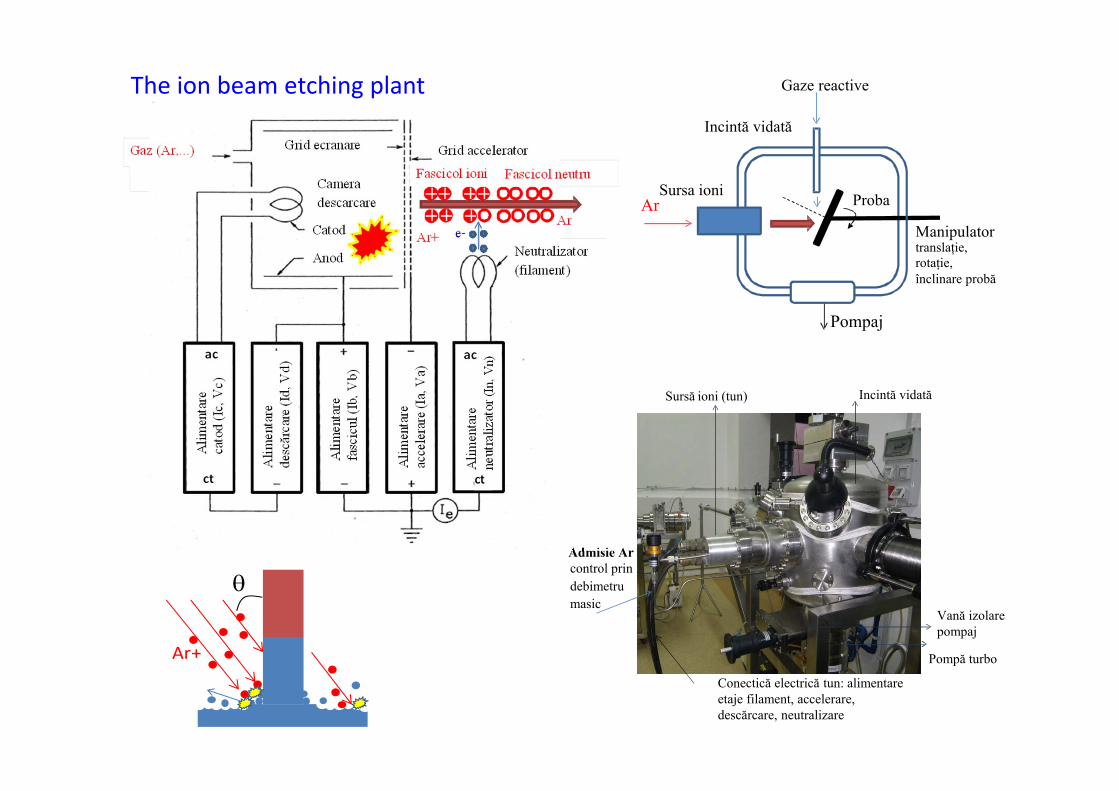
The ion beam etching plant
Ar+
Sursa ioni
Pompaj
Incintă vidată
ProbaAr
Gaze reactive
Manipulatortranslație,rotație,înclinare probă
Sursă ioni (tun)
Admisie Arcontrol prindebimetrumasic
Conectică electrică tun: alimentare etaje filament, accelerare, descărcare, neutralizare
Incintă vidată
Pompă turbo
Vană izolarepompaj
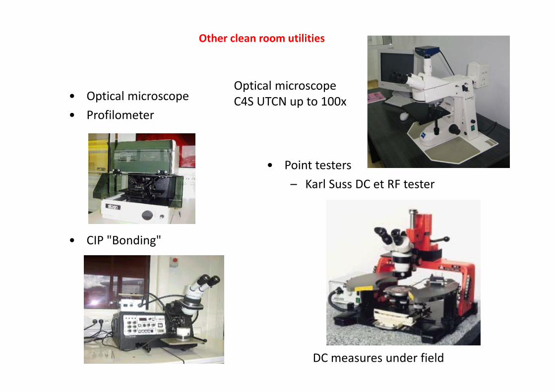
Other clean room utilities
• Optical microscope• Profilometer
• CIP "Bonding"
• Point testers– Karl Suss DC et RF tester
Optical microscope C4S UTCN up to 100x
DC measures under field
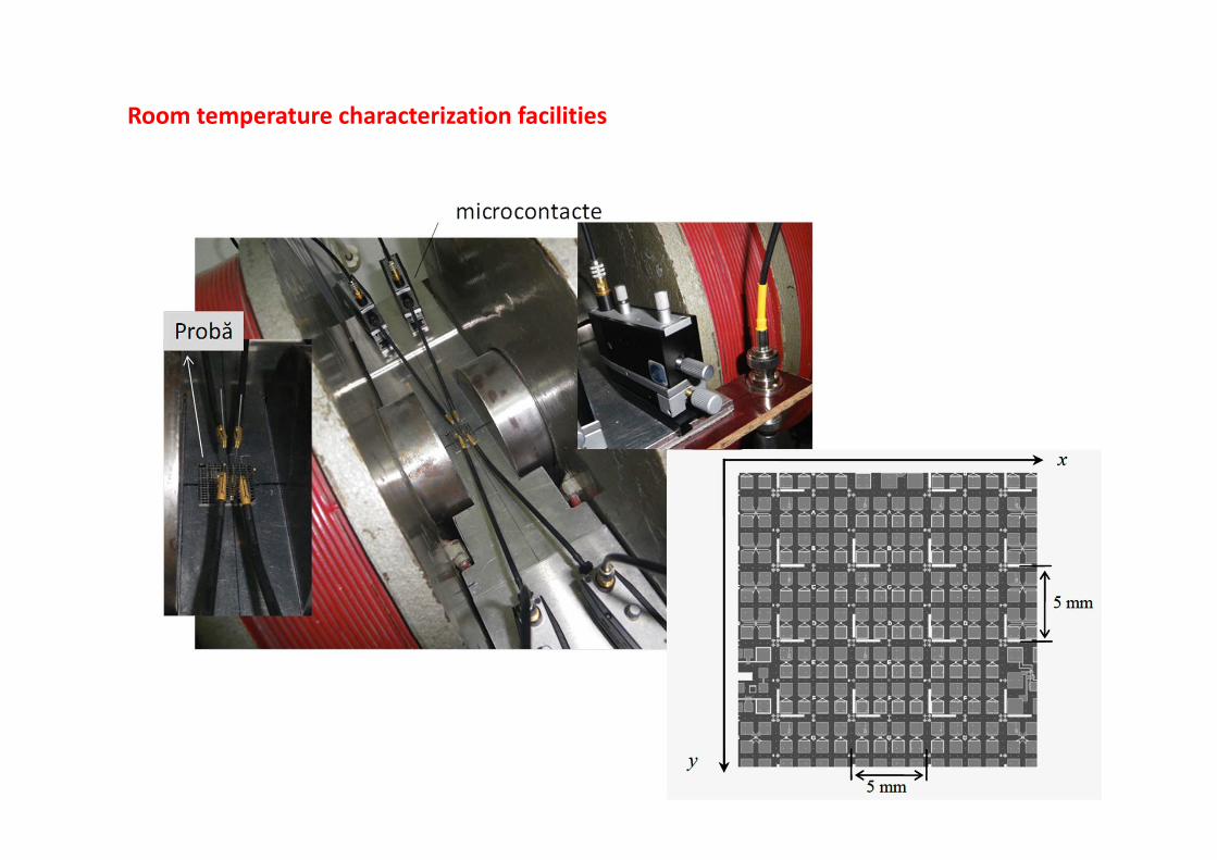
Room temperature characterization facilities
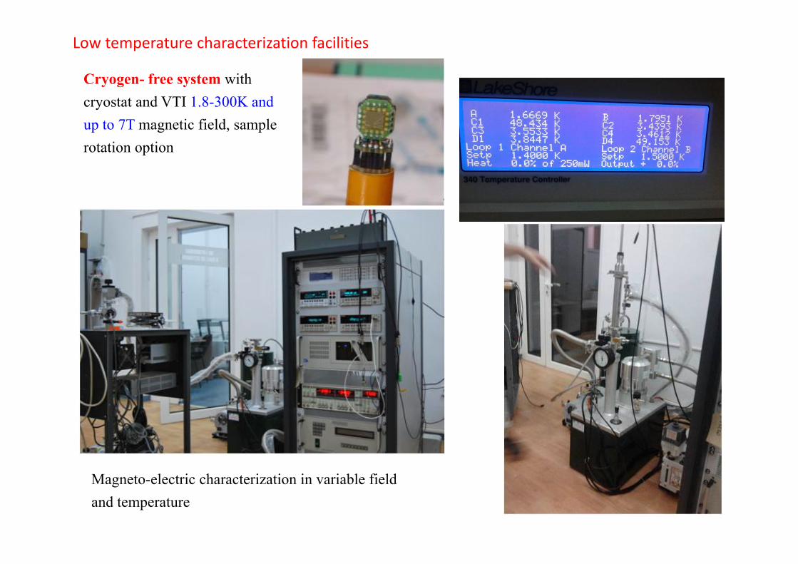
Cryogen- free system with cryostat and VTI 1.8-300K and up to 7T magnetic field, sample rotation option
Magneto-electric characterization in variable field and temperature
Low temperature characterization facilities
Thanks!
Tomorrow morning: TMR