Embed Size (px)
Citation preview
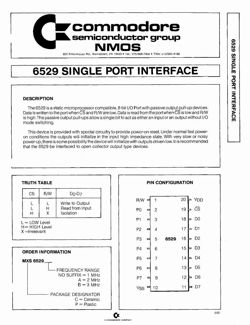
commodoresemiconductor group
INI M O S950 Rittenhouse Rd., Norristown, PA 19403 • Tel.: 215/666-7950 • TWX: 510/660-4168
6529 SINGLE PORT INTERFACE
DESCRIPTION
The 6529 is a static microprocessor compatible, 8-bit I/O Port with passive outputpull-up devices. Data is written to the port when CS and R/Ware low. Data is read from the port when CS is low and R/W is high. The passive output pull-ups allow a single bit to act as either an input or an output without I/O mode switching.
This device is provided with special circuitry to provide power-on reset. Under normal fast power- on conditions the outputs will initialize in the input high impedance state. With very slow or noisy power-up, there is some possibility the device will initialize with outputs driven low. It is recommended that the 6529 be interfaced to open collector output type devices.
TRUTH TABLE
CS R/W D0-D7
L L Write to OutputL H Read from InputH X Isolation
L = LOW Level H= HIGH Level X ^Irrelevant
ORDER INFORMATION
MXS 6529.
FREQUENCY RANGE NO SUFFIX = 1 MHz
A = 2 MHz B = 3 MHz
PACKAGE DESIGNATOR C = Ceramic P = Plastic
PIN CONFIGURATION
R/W = 1 20 =■ v d d
P0 = 2 19 =3 CS
P1 «= 3 18 =3 DO
P2 = 4 17 => D1
P3 «= 5 6529 16 =. D2
P4 = 6 15
00Q
P5 « 7 14 = D4
P6 = 8 13 a D5
P7 = 9 12 =» D6
Vss “ 10 11 =» D7
c *A COMNAOOORE C O M PA N Y
4/81
6529 SINGLE
PORT IN
TERFA
CE
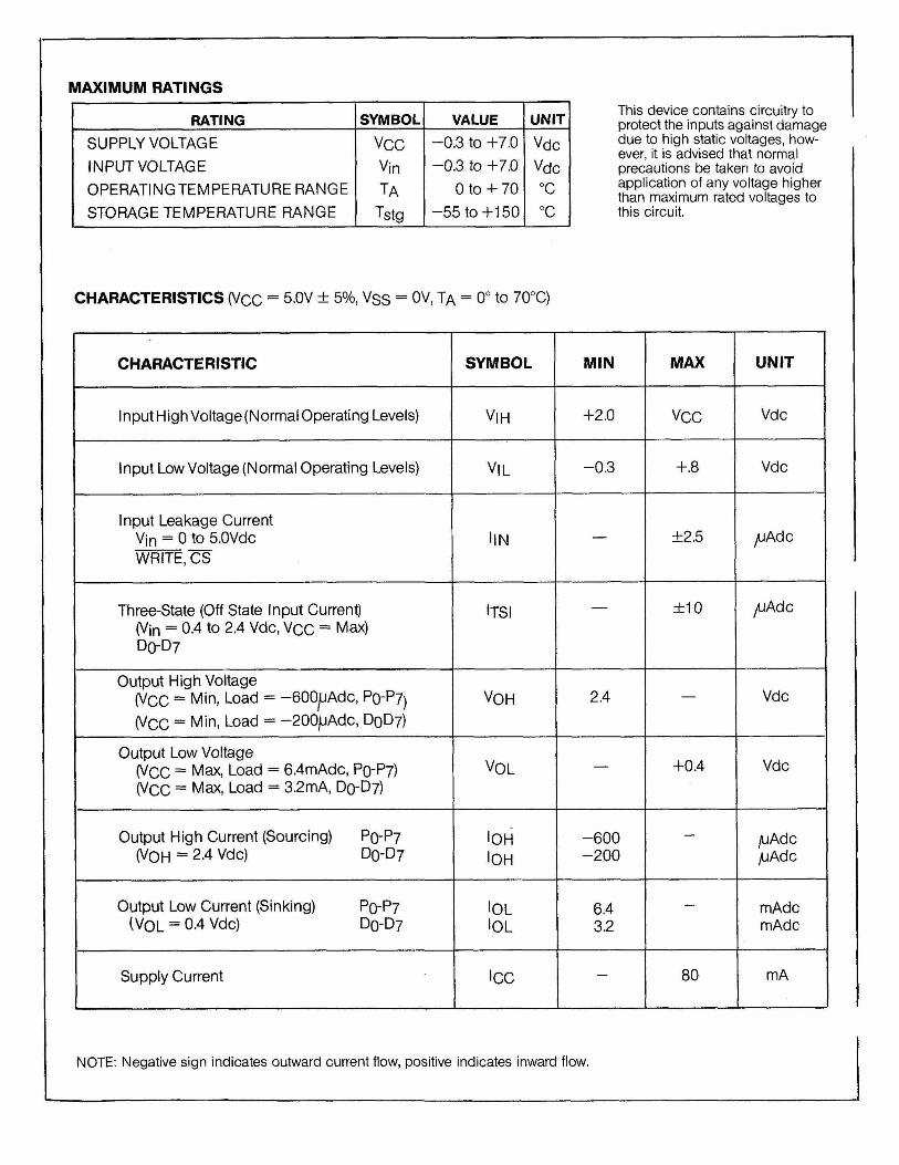
MAXIMUM RATINGS
RATING SYMBOL VALUE UNIT
SUPPLY VOLTAGE INPUT VOLTAGEOPERATING TEMPERATURE RANGE STORAGE TEMPERATURE RANGE
VccVinta
Tstg
-0 .3 to +7.0 -0 .3 to +7.0
0 to + 70 -5 5 to +150
VdcVdc°C°C
This device contains circuitry to protect the inputs against damage due to high static voltages, however, it is advised that normal precautions be taken to avoid application of any voltage higher than maximum rated voltages to this circuit.
CHARACTERISTICS (VCC = 5.0V ± 5%, Vss = 0V, Ta = 0° to 70°C)
CHARACTERISTIC SYMBOL MIN MAX UNIT
Input High Voltage (Normal Operating Levels) V|H + 2.0 Vcc Vdc
Input Low Voltage (Normal Operating Levels) VlL -0.3 +.8 Vdc
Input Leakage Current Vjn = 0 to 5.0Vdc WRITE, CS
IlN — ±2.5 yUAdC
Three-State (Off State Input Current) (Vjn = 0.4 to 2.4 Vdc, V cc = Max) D0-D7
iTSI — ± 10 /uAdc
Output High Voltage(Vcc = Min> Loacl = -OOO^Adc, P0-P7)(Vcc = Min, Load = -200jUAdc, D0D7)
VOH 2.4 Vdc
Output Low Voltage (VCC = Max> Load = 6.4mAdc, P0-P7) (Vcc = Max, Load = 3.2mA, D0-D7)
VOL — •0.4 Vdc
Output High Current (Sourcing) P0-P7 (VOH = 2.4 Vdc) D0-D7
lOHlOH
-6 0 0-2 0 0
— /uAdcpAdc
Output Low Current (Sinking) P0-P7 (V o l = 0.4 Vdc) D0-D7
lOLlOL
6.43.2
— mAdcmAdc
Supply Current ICC — 80 mA
NOTE: Negative sign indicates outward current flow, positive indicates inward flow.
READ CYCLE TIMING DIAGRAM
CS
D0-D7
INPUT
R/W
mnnh
t-tpDS*
~ \ rJ L
■*-K -
'co■ta c c
•G3
* tw cs< ~ tpV D
C
Tunmnmmih'tOTD '
m
■tw c h
tRC
READ CYCLE CHARACTERISTICS
1 MHz 2MHz 3MHz
Symbol Parameter MIN MAX MIN MAX MIN MAX UNITS
tACC Access time 450 225 160 nS
tc o Chip Select to Output Valid 450 225 160 nS
tOTD Chip Deselected to Output Off 20 120 20 120 20 120 nS
tPDS Peripheral Data Set-Up 120 60 40 nS
tPVD Peripheral Data Valid 150 150 150 nS
tw cs Write to CS Setup 0 0 0 nS
tWCR Write to CS Hold 0 0 0 nS
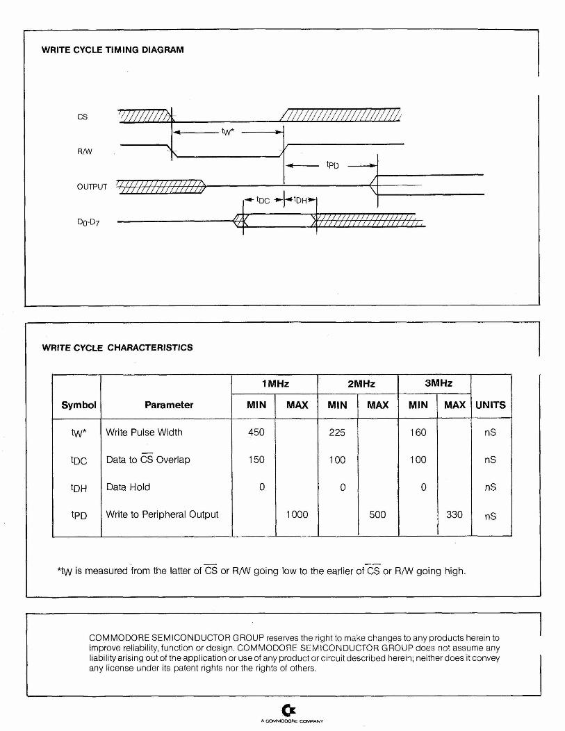
WRITE CYCLE CHARACTERISTICS
Symbol Parameter
1 MHz 2MHz 3MHz
UNITSMIN MAX MIN MAX MIN MAX
tw* Write Pulse Width 450 225 160 nS
tDC Data to CS Overlap 150 100 100 nS
tDH Data Hold 0 0 0 nS
tPD Write to Peripheral Output 1000 500 330 nS
*tw is measured from the latter of CS or R/W going low to the earlier of CS or R/W going high.
COMMODORE SEMICONDUCTOR GROUP reserves the right to make changes to any products herein to improve reliability, function or design. COMMODORE SEMICONDUCTOR GROUP does not assume any liability arising out of the application or use of any product or circuit described herein; neither does it convey any license under its patent rights nor the rights of others.
c *A C O M M O D O R E C O M P A N Y