Embed Size (px)
Citation preview

COGNITIVE RADIO TRANSMITTER
WITH A BROADBAND CLEAN
FREQUENCY SPECTRUM
Saqib Subhan

COGNITIVE RADIO TRANSMITTER
WITH A BROADBAND CLEAN
FREQUENCY SPECTRUM
Saqib Subhan

The Graduation Committee:
Chairman:
Prof.dr.ir. P.G.M. Apers University of Twente Secretary:
Prof.dr.ir. P.G.M. Apers University of Twente
Promotor:
Prof.dr.ir. B.Nauta University of Twente
Assistant Promotor:
Dr.ing. E.A.M. Klumperink University of Twente
Members:
Prof.dr.ir. P.G.M. Baltus Eindhoven University of Technology
Prof.dr. R.B. Staszewski Delft University of Technology
Prof.dr.ing. P.J.M. Havinga University of Twente
Prof.dr.ir. F.E. van Vliet TNO/ University of Twente
CTIT Ph.D. Thesis Series No. 14-310.
Center for Telematics and Information Technology.
P.O. Box 217, 7500 AE
Enschede, The Netherlands.
This research is supported by the Higher Education Commission
(HEC), Government of Pakistan.
This research is partly supported by the Dutch Technology
Foundation (STW), which is part of the Netherlands
Organization for Scientific Research (NWO) and partly funded
by the Ministry of Economic Affairs, Agriculture and Innovation
(08081 ADREM Radio) .
Title: Cognitive Radio Transmitter with a Broadband Clean Frequency Spectrum
ISBN: 978-90-365-3677-6.
ISSN: 1381-3617.
DOI: 10.3990/1.9789036536776.
Copyright © 2014 Saqib Subhan, Enschede, The Netherlands.

COGNITIVE RADIO TRANSMITTER
WITH A BROADBAND CLEAN
FREQUENCY SPECTRUM
DISSERTATION
to obtain
the degree of doctor at the University of Twente,
on the authority of the rector magnificus,
prof. dr. H. Brinksma,
on account of the decision of the graduation committee,
to be publicly defended
on Wednesday the 2nd
of July 2014 at 16:45
by
Saqib Subhan
born on 2nd
June 1981
in Lahore, Pakistan

This dissertation has been approved by
The Promotor: Prof. dr. Ir. Bram Nauta
Assistant Promotor: Dr.ing. Eric. A.M. Klumperink


i
ABSTRACT The tremendous increase in wireless communication over the last few decades has led to a
congestion of the radio frequency (RF) spectrum, which is utilized for transmission and
reception of information. As suitable RF spectrum is scarce, attempts are being made to use
the RF spectrum in a more intelligent efficient way. A Cognitive Radio addresses this
problem by Dynamic Spectrum Access, i.e. measure which spectrum is temporarily locally
free and then use it. The Cognitive Radio transmitter needs to be flexible to be able to
transmit where ever there is free spectrum available.
Conventional transmitters not only produce the desired upconverted information signal but
also many unwanted harmonics of the local oscillator (LO) and distortion products related
to the baseband signal. These unwanted products have been usually suppressed using
dedicated RF filters which are narrowband and are not flexible. For Cognitive Radio
transmitters flexibility is a key requirement, and hence other techniques are wanted to
suppress unwanted products, without using the inflexible filters. Moreover, agile operation
of the cognitive radio transmitter in a broad band is wanted.
Previous research has shown that polyphase multipath circuits can in principle cancel a
large number of harmonics and distortion products. However, a solution for wideband
polyphase baseband signal generation including digital-to-analog conversion and filtering
was lacking. Moreover, the upconversion was done using a large number of paths which
takes quite some chip area and is not very power efficient. In this work a less complex and
more power efficient implementation of this technique is proposed. The proposal is actually
based on a combination of three techniques, namely: 1) 8-path polyphase upconversion, 2)
tuning of the LO duty cycle ratio to close to 7/16 and 3) a tunable first order RF filter. The
combination of these three techniques allows to suppress all unwanted products to more
than 40dB below the desired signal. It is possible to improve this further if a tunable RLC
network with high quality factor is used at the RF output.
The multiphase baseband signals required for an 8-path upconversion can be generated
using a simplified vector modulator type of architecture. In order to allow for a Spurious
Free Dynamic Range of 50dB, the use of a Digital to Analog Converter (DAC) with a
resolution of at least 7 bits is proposed. It is shown that it is possible to cancel the first
dominant DAC image by using a polyphase DAC architecture, which relaxes analog
reconstruction filtering requirements.
To verify the functionality of the proposed techniques, a flexible 8-path transmitter chip
was fabricated in a 160 nanometer CMOS technology. The transmitter works over 3
octaves in frequency from 100MHz to 800MHz. Measurements show that the frequency

ii
agile transmitter achieves a broadband clean output spectrum where all unwanted products
are at least 40dB below the wanted transmit signal. This is the first polyphase multi-path
transmitter combining the baseband multi-phase generation and RF circuit on one chip.
Compared to other harmonic rejection transmitter designs with similar frequency range, it is
more power efficient and has better LO leakage and image rejection. Note that this chip
suppresses ALL LO harmonics and distortion products for ALL frequencies, without any
external filters.

iii
SAMENVATTING
De enorme toename van draadloze communicatie in de afgelopen decennia begint te leiden
tot verstopping van het radio frequentie (RF) spectrum dat wordt gebruikt voor het
verzenden en ontvangen van informatie. Omdat geschikt RF spectrum schaars is, probeert
men het spectrum op een meer intelligente efficiente wijze te gebruiken. Een Cognitieve
Radio doet dit via dynamische spectrum toegang door te meten waar spectrum (tijdelijk
plaatselijk) vrij is en dan te benutten. Een Cognitieve Radio zender moet daarvoor flexibel
zijn qua zendfrequentie.
Zenders dienen idealiter alleen het basisband informatie signaal op te converteren naar de
zendfrequentie. Daarbij ontstaan echter ook vele ongewenste nevenproducten, ondermeer
harmonischen van de voor het converteren gebruikte lokale oscillator (LO) en
vervormingsproducten van het basisband signaal. Deze ongewenste nevenproducten
worden in een conventionele zender meestal onderdrukt met behulp van speciale RF-filters
die smalbandig zijn en niet felxibel verstembaar. Voor een cognitieve radio zender is
flexibiliteit een eerste vereiste, zodat vaste filters onpraktisch zijn. Darom zijn er nieuwe
technieken nodig, die een flexibele zendfrequentie mogelijk maken zonder het radio
spectrum onnodig te vervuilen.
In voorgaand onderzoek is aangetoond dat polyfase multi-pad circuits in principe in staat
zijn een groot aantal harmonischen en distorsieproducten te onderdrukken. Een oplossing
voor de breedbandige polyfase basisband signaalgeneratie ontbrak echter. Ook was een erg
groot aantal signaalpaden nodig, wat nadelig is voor chipoppervlakte en energie gebruik. In
dit onderzoek wordt een meer compacte en energie-efficiënte uitvoering van deze techniek
voorgesteld op basis van een combinatie van drie technieken: 1 ) 8-pad polyfase frequentie
conversie; 2) afregeling van de duty cycle van het LO signaal op ongeveer 7/16; 3)
toepassing van een eerste order laagdoorlaat RF filter met regelbare capaciteit. De
combinatie van deze drie technieken kan alle LO harmonischen en distorsie producten
tenminste 40dB onderdrukken ten opzichte van het gewenste zendsignaal. Het is mogelijk
dit verder te verbeteren als een afstembaar R-L-C netwerk met hoge kwaliteitsfactor
gebruikt wordt op de uitgang. Het benodigde polyfase basisband signaal kan worden
gegenereerd met behulp van een vereenvoudigde vectormodulator in het digitale domein.
Om een “Spurious Free Dynamic Range” van meer dan 50dB mogelijk te maken, wordt
voorgesteld een digitaal-analoog converter (DAC) met een resolutie van tenminste 7 bits te
gebruiken. Tevens wordt aangetoond dat het mogelijk is om de eerste DAC image the
onderdrukken met behulp van een meerfase DAC architectuur, waardoor minder analoge
reconstructie filtering nodig is achter de DAC

iv
.
Om de werking van de voorgestelde technieken te demonstreren is een chip ontworpen en
gefabriceerd in een 160 nanometer CMOS-technologie. De zender werkt over 3 octaven in
frequentie; van 100MHz tot 800MHz. Deze flexibele zender blijkt daarbij in staat
breedbandig alle ongewenste nevenproducten meer dan 40dB onder het gewenste
zendsignaal te houden. Dit is de eerste chip die een polyfase multi-pad zender
implementeert inclusief de meerfasige basisband signaalgeneratie. Vergeleken met andere
zender chips die harmonischen onderdrukken in hetzelfde frequentiebereik, is deze chip
zuiniger terwijl de LO-signaal emissie en spiegelonderdrukking ook beter is. Met name is
bijzonder dat deze chip ALLE LO harmonischen en distorsie producten breedbandig
onderdrukt voor ALLE frequenties, zonder gebruik te maken van externe filters.

v
Contents
ABSTRACT ......................................................................................................................... I
SAMENVATTING ............................................................................................................. III
1 INTRODUCTION ........................................................................................................1
1.1 PROBLEM DEFINITION ............................................................................................2
1.2 TRANSMITTER TERMINOLOGY ...................................................................................4
1.2.1 Linearity .......................................................................................................4
1.2.2 Error Vector Magnitude ................................................................................5
1.2.3 Spectral Mask ...............................................................................................5
1.2.4 Efficiency ......................................................................................................5
1.2.5 LO Harmonics ...............................................................................................6
1.2.6 DAC replica images .......................................................................................7
1.2.7 Output Noise ................................................................................................7
1.3 SCOPE OF THE THESIS .............................................................................................7
1.4 PREVIEW OF THE THESIS ..........................................................................................8
2 TRANSMITTER ARCHITECTURES.............................................................................. 13
2.1 MULTIMODE TRANSMITTER ARCHITECTURES REVIEW ................................................... 13
2.2 HARMONIC AND DISTORTION SUPPRESSION TECHNIQUES .............................................. 16
2.2.1 Polyphase Multipath Technique .................................................................. 18
2.3 COGNITIVE RADIO TRANSMITTER REQUIREMENTS ........................................................ 22
2.4 CONCLUSIONS .................................................................................................... 23
3 POLYPHASE MULTIPATH TRANSMITTER SYSTEM DESIGN ....................................... 29
3.1 POLY-PHASE MULTIPATH SYSTEM ANALYSIS ............................................................... 29
3.1.1 Multipath System with a First order RC filter at the output. ......................... 31
3.2 EIGHT PATH TRANSMITTER .................................................................................... 32
3.2.1 Eight path Transmitter and tunable RF Filter ............................................... 35
3.3 EFFICIENCY VS. DUTY CYCLE .................................................................................... 40
3.4 GENERATING LO DUTY CYCLE ................................................................................ 43
3.5 EFFECT OF PHASE MISMATCH ................................................................................. 44
3.6 CONCLUSION...................................................................................................... 45
4 MIXED-SIGNAL SYSTEM DESIGN ............................................................................. 47
4.1 MULTIPHASE BASEBAND GENERATION...................................................................... 48
4.2 DAC RESOLUTION IMPACT ON A POLY-PHASE MULTIPATH TRANSMITTER .......................... 53
4.2.1 Multipath Technique applied to a Uniform DAC with ideal Phase Shifter ...... 53

vi
4.2.2 Multipath Technique applied to a Uniform DAC with Mixer as Phase Shifter 57
4.3 DAC REPLICA IMAGE CANCELLATION ....................................................................... 59
4.3.1 Suppression of DAC images due to summation of parallel DAC output ......... 59
4.3.2 Suppression of DAC images in Polyphase Multipath Upconversion ............... 63
4.4 DAC IMPLEMENTATION ........................................................................................ 78
4.4.1 N parallel DACs........................................................................................... 78
4.4.2 One DAC with de-interleaving ..................................................................... 80
4.5 DIGITAL INTERPOLATION FILTER .............................................................................. 81
4.5.1 Digital Filter Design .................................................................................... 82
4.6 CONCLUSION...................................................................................................... 85
5 POLYPHASE MULTIPATH TRANSMITTER IMPLEMENTATION ................................... 87
5.1 BASEBAND GENERATION ....................................................................................... 88
5.2 8-PHASE LO GENERATION ..................................................................................... 90
5.2.1 Generating 1/8 duty cycle for sample & hold switch .................................... 91
5.3 DUTY-CYCLE CONTROL CIRCUIT DESIGN .................................................................... 92
5.3.1 Duty-Cycle for the required accuracy ........................................................... 93
5.3.2 Duty-Cycle over a Frequency Range ............................................................ 95
5.3.3 Duty-Cycle variation with Temperature ....................................................... 95
5.4 REPLICA BIASING ................................................................................................. 96
5.5 MIXERS ............................................................................................................ 97
5.6 TUNABLE 1ST ORDER LOW-PASS FILTER.................................................................... 98
5.7 MEASUREMENT RESULTS .................................................................................... 100
5.8 CONCLUSION.................................................................................................... 106
6 CONCLUSIONS ...................................................................................................... 111
6.1 SUMMARY AND CONCLUSIONS ............................................................................. 111
6.2 ORIGINAL CONTRIBUTIONS .................................................................................. 112
6.3 RECOMMENDATIONS FOR FUTURE WORK................................................................ 113
APPENDIX A .................................................................................................................. 115
APPENDIX B .................................................................................................................. 117
APPENDIX C .................................................................................................................. 121
ACKNOWLEDGEMENTS ................................................................................................. 124
LIST OF PUBLICATIONS.................................................................................................. 127
ABOUT THE AUTHOR .................................................................................................... 128

vii

viii

1
CHAPTER ONE
1 Introduction
The explosive growth in wireless communications has led to a plethora of wireless
communication standards. Mobile handsets now commonly support multi-band GSM,
WCDMA, WLAN, Bluetooth, GPS, FM radio and more. Laptops and tablets also
commonly support at least several WLAN radio standards, and more functionality is
continuously added. Radio standards have been proposed to serve different purposes. GSM
for example is mainly developed for voice calls using the terrestrial infrastructure,
Bluetooth for short distance personal area network data transfer and recent WLAN
standards for fast computer network access. New extended versions of standards are
regularly introduced to support new functionality or higher data rates (e.g. different WLAN
version like 802.11b, g, n). Each of the radio standards defines a communication protocol
and frequency band, which was conventionally supported by a dedicated integrated circuit
(IC) with external antenna and passive components to realize radio transceiver functionality
(transmit and receive). As the number of these standards grows, the cost and area required
to put all the ICs and associated components on one device also increases. Therefore there
is a need to somehow combine functionality and re-use hardware to support different
standards onto one IC. This has led to the concept of a Software Defined Radio (SDR) or its
more ideal version the Software Radio [1]. A SDR contains reconfigurable radio hardware,
where most of the functionality of the transceiver (transmitter and receiver) is defined in
software. To reuse the same hardware frontend, it must be flexible enough to meet the
requirements of all the different standards to be supported.
Each of the different protocols mentioned above uses a certain frequency band to send its
data. As an example the GSM protocol uses 800/900 MHz or the 1800/1900MHz frequency
band. Bluetooth, WLAN among others, communicates on the 2.4GHz band. The frequency
band a certain communication protocol uses is assigned by a regulating authority such as
the Federal communication commission (FCC) in the United States or the OFCOM in the
United Kingdom. Most of the terrestrial communication protocols are utilizing the
frequency spectrum upto around 6 GHz. Each operator of a communication infrastructure
has to buy a license from the regulator in the country where it is operating to have the right
to use that particular frequency spectrum. This can be very expensive [2] as there is limited
spectrum and there are quite some competitors. As shown in the FCC frequency allocation

2
table [3, 4] most of the usable bands have already been allocated to commercial users, i.e.
there seems to be a spectrum scarcity problem.
However studies [5] suggest that the spectrum is far from fully utilized for a given
timeframe at a particular location. Therefore, more efficient utilization of the frequency
spectrum may help to alleviate the spectrum scarcity problem. This led to the concept of
cognitive radio [6]. The cognitive radio (CR) would actively monitor the frequency
spectrum and look for unutilized frequency spots also known as white spaces. The
cognitive radio would then dynamically alter or set its transmission parameters such as
frequency, power etc, to be able to utilize those white spaces. This process is also called
Dynamic Spectrum Access. The key issue here is that the incumbent users (primary users)
of the frequency spectrum do not undergo any harmful interference during the whole
process.
The cognitive radio can be seen as an extension of the software defined radio. Both require
a flexible radio frontend to cater to different communication standards at different
transmission frequencies. This thesis focuses on the transmitter part of a cognitive radio
transceiver. The challenge facing such a transmitter is defined in the next section.
1.1 Problem Definition The main task of a Radio Frequency (RF) transmitter is to shift a low frequency baseband
signal to a higher RF signal. Moreover, the transmitter should also amplify the input signal,
in order to provide the required power to the antenna load. This can be represented in the
frequency spectrum as shown in Figure 1.1: two tones at the input around DC are up-
converted to the output around a so-called “Local Oscillator” frequency, or simply
abbreviated as “LO”. Up-conversion can in theory be realized using linear but time-variant
networks containing switches driven by the LO. The switching can be modeled as a
multiplication with a square-wave, which will not only lead to up-conversion around LO,
but also to up-conversion around higher harmonics of LO. Moreover, as the switching but
also the amplification is realized exploiting nonlinear transistors, extra unwanted terms due
to non-linearity are produced at the output. Clearly such terms are problematic, as they
occupy extra spectrum and pose interference to other users.
A common direct conversion transmitter architecture can be realized by the blocks given in
Figure 1.2. A Digital to Analog Converter (DAC) converts the digital baseband to the
analog domain, while the Low Pass Filter (LPF) filter removes or suppresses the undesired
frequency components coming out of the DAC. The mixer and the Power Amplifier (PA)
provide the frequency translation and signal amplification

3
Figure 1.1. Ideal RF Transmitter Frequency Spectrum
Figure 1.2. Direct Conversion Transmitter
The output spectrum of such kind of a transmitter can be similar to the one shown in Figure
1.3, which differs significantly from the output spectrum of an ideal transmitter shown in
Figure 1.1. Here apart from the desired signal around the LO frequency, there are other
unwanted frequency components such as IM3 (3rd order inter-modulation distortion), HD3
(3rd order harmonic distortion), DACimg (remnants of the signal image around the DAC
clock which have not been completely filtered) and LO harmonics (due to time-variant
behavior of switching mixers).
In order to reduce these unwanted spectral components, an RF Band Pass Filter (BPF)
could be employed at the output of the transmitter as shown in Figure 1.4. This BPF can
suppress most of these unwanted components, but the problem for a cognitive or software
defined radio application is the desire for flexibility in frequency. Most off-chip filters are
dedicated for one particular frequency band, so a multiband transmitter would require
multiple of these filters. External filters would also add to the cost and size of the Integrated
circuit. On chip filters generally have a limited tuning range, so they are also not very
flexible. Additionally if inductors are used to implement these filters, they would also
consume a lot of chip area. Since a cognitive radio transmitter has to cover a wide band, a
solution is desired which can be flexible and can be integrated on chip while not requiring
separate off chip filters for each RF band.

4
Figure 1.3 An output spectrum of the transmitter in Figure 1.2
A possible solution to overcome these challenges, could materialize in the form of switched
capacitor (SC) N-path filter [7], which can achieve very high Q, while being tunable in
center frequency by its clock frequency. The idea of N-path filters is quite old [8], but
currently experiencing a revival [9-11]. They are flexible and easy to integrate on chip.
However, handling sufficient RF power might still be challenging, moreover they still
produce uncancelled harmonics. Another possible solution could be based on the use of
MEMS based devices for use in tunable filters [12, 13], but these suffer from limitations in
tunability and linearity. Another possible solution which could be able to overcome the
problems mentioned above is the use of very high frequency digital to analog converters
(DACs). Recently they have become very competitive [14-16]. Although the harmonic
problem would still be there, and power consumption may still be of concern.
1.2 Transmitter Terminology Some key transmitter related terminologies that will be used in this thesis are introduced
below, whereas their relevance for cognitive radio is also discussed briefly.
1.2.1 Linearity
As mentioned in section 1.1, the baseband to RF upconversion process results in
nonlinearity. This results in distortion, both intermodulation distortion and harmonic
distortion, which may cause interference to other users. Harmonic distortion is due to the
baseband distortion combining with the LO harmonics to appear at the RF. Intermodulation
distortion mainly effects nearby channels, and degrades the error vector magnitude (EVM)
or bit error rate. Depending upon the input spectrum, the harmonic distortion may appear
further away in the output spectrum from the desired channel, but can interfere with other
users of the frequency spectrum too, especially if sufficient filtering is not present.

5
Figure 1.4 An RF BPF can suppress the unwanted spectral components.
1.2.2 Error Vector Magnitude
Due to several transmitter impairments, e.g. nonlinearity in the signal path, I-Q imbalance
and (phase) noise, the transmitted constellation points of a digitally modulated transmit
signal deviate from their ideal locations. The magnitude of the error vector between the
ideal constellation point and the point to be measured, normalized by the ideal signal vector
defines the error vector magnitude. This performance parameter is often used to judge the
overall suitability of a transmitter to transmit high-order complex signal constellations.
1.2.3 Spectral Mask
The spectral mask quantifies how much power a transmitter is allowed to transmit as a
function of frequency. An arbitrary spectral mask is shown in Figure 1.5, where the top of
the dotted line defines the maximum allowed signal power, while the decreasing sides of
the spectral mask define the maximum radiated power in neighboring and far-out bands.
This mask defines the limit on the acceptable harmonics and distortion power. The spectral
mask requirements for a Cognitive Radio Transmitter are discussed in Chapter 2 section
2.3.
1.2.4 Efficiency
The power efficiency is a ratio between useful RF output power and the required DC power
consumed to produce this power. Often, there is a trade-off between efficiency and
linearity.

6
Figure 1.5. An arbitrary Spectral Mask
E.g. a transistor biased as class-A amplifier is more linear than for class-B or class-C
biasing [17] but less power efficient. We will use class-A amplifiers in this thesis as
linearity is important for complex modulated signals with high spectral efficiency [17].
The efficiency could be just confined to the final output amplifier. In that case it is usually
defined as the drain efficiency. Here single tone output is assumed.
Drain Efficiency = PRF/PDC, amp
where PRF, is the sinusoidal output power and PDC,amp is the DC power consumed in the
output amplifier. However, there can also be significant DC power consumption (PDC,BB) in
the baseband (BB) filters and amplifiers, mixers (PDC,mixers) or multiphase LO generation
(PDC,LOGEN). The total efficiency of the upconversion can then be defined as:
Total Efficiency = PRF/ (PDC,amp+ mixer + PDC,LOGEN + PDC,BB)
The power consumed in the Digital to analog converting function may also be included in
the power consumption of the baseband paths, especially for completely digital solutions.
An analysis on efficiency of the upconverter presented in this thesis is given in Chapter 3
section 3.3, while the measurement of the total efficiency of the implemented Cognitive
Radio Transmitter is presented in Table 5.1. The output power requirements for a cognitive
radio transmitter are discussed in section 2.3.
1.2.5 LO Harmonics
Frequency translation in transceivers usually takes place due to mixers, which shift the
frequency up (in case of transmitters) or down (in case of receivers). Most of these mixers
are implemented using hard switching mixers as they provide higher conversion gain and
better linearity compared to soft switching mixers. Hard switching results in harmonics of
ωLO 3ωLO 5ωLO
Desired Signal
Distortion
Spectral Mask
f
Mag
nitu
de
7
the LO frequency which can be dominant, if they are not appropriately suppressed.
Techniques to suppress these harmonics are discussed in chapters 2 and 3.
1.2.6 DAC replica images
When the digital baseband is converted to the analog domain via a Digital to analog
converter (DAC), replica images of the desired signal occur around the sample frequency of
the DAC. If appropriate filtering is not present they can become dominant and interfere
with other users of the frequency spectrum. DAC replica images can be suppressed by
baseband filtering or by baseband filtering in combination with increasing the sample rate
of the digital baseband via digital interpolation (see chapter 4).
1.2.7 Output Noise
Just like any other radiation, transmitter output noise may increase the noise floor of other
radio devices and should be limited in value. The noise emanating from the transmitter can
have several causes, e.g. wideband thermal noise, phase-noise of the mixer LO-signal and
or up-converted thermal noise and 1/f noise of various components utilized for the
upconversion and amplification. Noise at the output could also be due to the quantization
noise due to limited DAC resolution. In conventional transmitters the thermal noise is often
dominant in the frequency spectrum far away from the desired channel, while the
quantization noise, phase noise and flicker noise is more dominant close to the desired
channel. The Quantization noise can be reduced by increasing the DAC resolution, or by
increasing the baseband filter order.
1.3 Scope of the thesis Section 1.1 presented challenges facing the design of a Cognitive Radio RF Transmitter.
The state-of-the-art and previous work on flexible transmitter architectures will be
discussed in chapter 2 in detail. One of the transmitter architectures discussed there is the
polyphase multipath technique on which the present work will build. It will be shown that
this technique can simultaneously suppress local oscillator (LO) harmonics and sideband
products originating from time variant mixer behavior, as well as many distortion products
due to nonlinearity. This can in principle be done without any dedicated filtering, which is
a nice asset for cognitive radio. If the number of signal paths is increased, a larger number
of harmonics and sidebands can be suppressed. An 18-path up-converter [18] can suppress
uptill the 17th harmonic of the LO. However the generation of 18 LO phases limits the
frequency range and consumes significant power. Moreover, in [18] the multiphase

8
baseband signals required to drive the multiple mixers were generated off chip. Actually,
only single-tone sine wave was used, and efficient multi-phase baseband signal generation
was recommended as “future work”. We will motivate in chapter 3 that it makes sense to
reduce the number of paths, to reduce complexity in terms of the number of baseband
signals and hence the number of DACs and baseband filters. Hence, the aim will be to
reduce the number of paths while maintaining or improving the harmonic suppression
characteristics. It will be shown that duty cycle control of the LO can nicely complement
the multipath polyphase technique if we choose an 8-path transmitter.
The main goal of this thesis is to explore design options for a flexible RF transmitter which
does not require dedicated RF filters to suppress the harmonics and distortion products
emanating from an upconversion process. The thesis builds upon the polyphase multipath
concept, previously proposed in [19]. After a critical evaluation of several design options, a
transmitter architecture is proposed that exploits LO duty-cycle control combined with an
8-path polyphase up-converter. Switched transconductor mixers [20] directly driving the
antenna are used for wideband upconversion. If the antenna does not sufficiently reduce far
out residual signals or noise a simple filter can be added. Depending on the requirements
and frequency range, a first order low-pass filter can be added or an elementary L-C band
pass filter, with variable capacitance. A variable high-frequency external clock is used for
generating the multi-phase on-chip clock needed for driving the mixer switches. The
frequency range targeted is the below 900 MHz frequency bands, which are being opened
up for unlicensed devices [21, 22]. To demonstrate the effectiveness of the techniques, a
demonstrator IC is designed which exploits one (external) DAC to generate all the
baseband phases in a time-interleaved fashion. The chip contains the de-interleaving
hardware, baseband buffers with baseband filters, upconversion power-mixers and the LO-
generation hardware including the duty-cycle control. Measurements over multi octaves of
frequency (100-800 MHz) show that all unwanted products can be kept <-40dBc at better
power efficiency than competing designs, including [18].
1.4 Preview of the thesis
In chapter 2, a brief overview of some of the recent transmitter architectures which focus on
flexible transmitter concepts is presented. This chapter also presents some harmonic
suppression techniques used in literature. The properties of the Polyphase Multipath
Technique are reviewed and it is motivated why this technique is used as a basis for the
flexible transmitter concept IC design presented later in the thesis.
In Chapter 3, design options for the implementation of the Polyphase Multipath technique
[18] are considered and the motivation for selecting an 8-path transmitter is presented. This

9
choice is largely affected by the benefits of a particular duty cycle of the LO, which is a
degree of freedom in the suppression of the harmonics. The efficiency versus duty cycle is
also analyzed to show that efficiency does not degrade significantly when selecting the
optimum duty cycle for harmonic suppression. Finally, LO-generation requirements and
phase mismatch are analyzed.
Chapter 4 discusses the mixed signal system design, which was not previously explored.
Functionally, the polyphase multipath upconversion requires polyphase baseband signals to
drive the mixers. Hence the generation of digital multiphase baseband signals is explored,
considering baseband DAC resolution requirements for the polyphase multipath transmitter.
The baseband DAC replica image cancellation properties in a polyphase multipath
upconversion system are analyzed, in an attempt to relax the baseband filtering
requirements. Also some baseband DAC implementation issues are discussed along with
interpolation filter requirements.
Chapter 5 presents the complete circuit design of the 8-path transmitter in a 160nm CMOS
process. Measurement results of the chip demonstrate the effectiveness of the proposed
circuit techniques and benchmark achieved results to that of competing design.
Chapter 6 presents the conclusions and suggestions for future work.
References
[1] J. Mitola, "The software radio architecture," Communications Magazine, IEEE, vol. 33, pp. 26-38, 1995.
[2] K. Binmore and P. Klemper, "The Biggest Auction Ever: the Sale of the British 3G Telecom Licences," Economic Journal, pp. 74-95, Mar 2002.
[3] FCC. FCC ONLINE TABLE OF FREQUENCY ALLOCATIONS. Available: http://transition.fcc.gov/oet/spectrum/table/fcctable.pdf
[4] NTIA. U.S. Frequency Allocation Chart Available: http://www.ntia.doc.gov/files/ntia/publications/2003-allochrt.pdf
[5] FCC. (2002). Report of the Spectrum Efficiency Working Group Available: http://transition.fcc.gov/sptf/files/SEWGFinalReport_1.pdf
[6] J. Mitola, III and G. Q. Maguire, Jr., "Cognitive radio: making software radios more personal," Personal Communications, IEEE, vol. 6, pp. 13-18, 1999.

10
[7] M. Darvishi, R. van der Zee, and B. Nauta, "Design of Active N-Path Filters," Solid-State Circuits, IEEE Journal of, vol. 48, pp. 2962-2976, Dec. 2013.
[8] L. E. Franks and I. W. Sandberg, "An Alternative Approach to the Realization of Network Transfer Functions: The N-Path Filters," Bell Sys. Tech. J., vol. 39, pp. 1321-1350, Sep. 1960.
[9] C. Andrews and A. C. Molnar, "A Passive Mixer-First Receiver With Digitally Controlled and Widely Tunable RF Interface," Solid-State Circuits, IEEE Journal of, vol. 45, pp. 2696-2708, 2010.
[10] A. Ghaffari, E. A. M. Klumperink, M. C. M. Soer, and B. Nauta, "Tunable High-Q N-Path Band-Pass Filters: Modeling and Verification," Solid-State Circuits, IEEE Journal of, vol. 46, pp. 998-1010, 2011.
[11] M. Darvishi, R. van der Zee, E. A. M. Klumperink, and B. Nauta, "Widely Tunable 4th Order Switched Gm-C Band-Pass Filter Based on N-Path Filters," Solid-State Circuits, IEEE Journal of, vol. 47, pp. 3105-3119, 2012.
[12] D. Ruffieux, J. Chabloz, M. Contaldo, C. Muller, F. Pengg, P. Tortori, et al., "A narrowband multi-channel 2.4 GHz MEMS-based transceiver," Solid-State Circuits, IEEE Journal of, vol. 44, pp. 228-239, Jan. 2009.
[13] S. Razafimandimby, C. Tilhac, A. Cathelin, A. Kaiser, and D. Belot, "An electronically tunable bandpass BAW-filter for a zero-IF WCDMA receiver," in Eur. Solid-State Circuits Conf. (ESS-CIRC), 2006, pp. 142-145.
[14] H. van de Vel, J. Briaire, C. Bastiaansen, P. Van Beek, G. Geelen, H. Gunnink, et al., "A 240mW 16b 3.2GS/s DAC in 65nm CMOS with <-80dBc IM3 up to 600MHz," in ISSCC Dig. Tech. Papers, 2014, pp. 206-207.
[15] G. Engel, S. Kuo, and Rose, "A 14b 3/6GS/s Current-Steering RF DAC in 0.18um CMOSwith 66dB ACLRat 2.9GHz," in ISSCC Dig. Tech Papers, 2012, pp. 458-459.
[16] E. Olieman, A. J. Annema, and B. Nauta, "A 110mW, 0.04mm2 , 11 GS/s 9-bit interleaved DAC in 28nm FDSOI with >50dB SFDR across Nyquist," in Symposium on VLSI Circuits, (accepted for publication) Honolulu, Hawaii, USA, 2014.
[17] B. Razavi, RF Microelectronics. Upper Saddle River, NJ: Prentice Hall, 1998. [18] R. Shrestha, E. A. M. Klumperink, E. Mensink, G. J. M. Wienk, and B.
Nauta, "A Polyphase Multipath Technique for Software-Defined Radio Transmitters," Solid-State Circuits, IEEE Journal of, vol. 41, pp. 2681-2692, 2006.
[19] E. Mensink, E. A. M. Klumperink, and B. Nauta, "Distortion cancellation by polyphase multipath circuits," IEEE Trans. Circuits Syst. II, Exp. Briefs, vol. 57, pp. 1785-1794, Sep. 2005.

11
[20] E. A. M. Klumperink, S. M. Louwsma, G. J. M. Wienk, and B. Nauta, "A CMOS switched transconductor mixer," Solid-State Circuits, IEEE Journal of, vol. 39, pp. 1231-1240, 2004.
[21] FCC, "Second Report and Order and Memorandum Opinion and Order In the Matter of Unlicensed Operation in the TV Broadcast Bands, Additional Spectrum for Unlicensed Devices Below 900 MHz and in the 3 GHz Band," Nov. 2008.
[22] FCC, "In the Matter of Unlicensed Operation in the TV Broadcast Bands Additional Spectrum for Unlicensed Devices Below 900MHz and in the 3GHz Band," Sep. 2010.

12

13
CHAPTER TWO
2 Transmitter Architectures There are various transmitter architectures which are targeted towards software defined or a
cognitive radio application. Aims vary; where some design focus on wideband linearity or
on issues like wideband LO generation, flexible digital image filtering or power control. A
few of the architectures aim for suppression or flexible filtering of LO harmonics. In this
chapter a brief overview is given of some of these transmitter architectures in recent
literature, focussing on multimode/ multi-standard aspects of their design. In section 2.1,
the transmitter architectures which claim to be multimode and targeted towards software
defined radio applications are discussed. These architectures do not aim for harmonic
suppression. The transmitter architectures which specifically aim for harmonic suppression
are discussed in section 2.2. In section 2.3, the out of band emission requirements of a
Cognitive Radio Transmitter are also discussed.
2.1 Multimode Transmitter Architectures Review Transmitters which claim to be multimode have the flexibility to cater to various baseband
bandwidths and modulation standards. A multimode transmitter based on the digital to RF
converter (DRFC) architecture [1] shown in Figure 2.1 focuses on making the digital
baseband flexible and also flexibility in the choice of frequency. This is accomplished by
removing the analog baseband filter and as the name suggests directly converts the digital
baseband to RF. The filtering is accomplished via oversampling which can be adapted. By
changing the oversampling ratio for different baseband bandwidths; the digital images and
noise can be suppressed, depending on how high the oversampling ratio is chosen. As
shown in Figure 2.2, in the DRFC architecture [1] there is no analog baseband and the
digital bits (D1, D2, …DN) are converted to the analog domain and simultaneously up-
converted via the LO to the RF output. The DAC function is therefore built into the DRFC.
Improvement in the Image rejection ratio and LO leakage are also claimed because of
improved matching of the I and Q paths of Figure 2.1. An RF filter would still be required
to suppress the harmonics of the LO.

14
Figure 2.1 Transmitter architecture based on the Digital to RF converter[1].
Figure 2.2. Digital to RF converter (DRFC) [1]
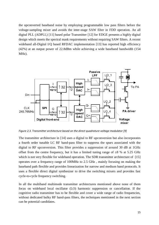
In [2], a multimode transmitter based on a direct quadrature voltage modulator (DQVM) in
combination with a highly oversampled baseband is proposed shown in Figure 2.3. Here the
oversampled baseband in combination with a relaxed low pass filter (LPF) attenuates the
DAC quantization noise and DAC images (see section 1.2.6 and 1.2.7). The passive mixer
is used to gain linearity benefits, i.e. achieve low EVM (see section 1.2.1 and 1.2.2). Here
also an RF filter is required if the LO harmonics are to be suppressed. In [3-5] a digital FIR
filter embedded with a digital to RF converter is used to suppress quantization noise. In [6]
a reconfigurable baseband path design is presented which can process WLAN, Bluetooth
and UMTS signals, thanks to a digitally programmable filter and DAC sampling frequency.
In [7] a 17 bit RFDAC is employed in a polar transmitter architecture, aiming to lower far
out noise and thus supporting both 2G and 3G standards. The WCDMA transmitter in [8]
also focuses on reducing the upconverter noise and thus removing the transmitter SAW
filter. The passive mixer [9] based 0.1-3GHz upconverter in [10] also focuses on reducing
15
the upconverted baseband noise by employing programmable low pass filters before the
voltage-sampling mixer and avoids the inter-stage SAW filter in FDD operation. An all
digital PLL (ADPLL) [11] based polar Transmitter [12] for EDGE presents a highly digital
design which meets the spectral mask requirements without requiring SAW filters. A recent
wideband all-Digital I/Q based RFDAC implementation [13] has reported high efficiency
(42%) at an output power of 22.8dBm while achieving a wide baseband bandwidth (154
MHz).
Figure 2.3. Transmitter architecture based on the direct quadrature voltage modulator [9]
The transmitter architecture in [14] uses a digital to RF upconversion but also incorporates
a fourth order tunable LC RF band-pass filter to suppress the spurs associated with the
digital to RF upconversion. This filter provides a suppression of around 30 dB at 1GHz
offset from the centre frequency, but it has a limited tuning range of ±8 % at 5.25 GHz
which is not very flexible for wideband operation. The SDR transmitter architecture of [15]
operates over a frequency range of 100MHz to 2.5 GHz , mainly focusing on making the
baseband path flexible and provides linearization for narrow and medium band protocols. It
uses a flexible direct digital synthesizer to drive the switching mixers and provides fast
cycle-to-cycle frequency switching.
In all the multiband multimode transmitter architectures mentioned above none of them
focus on wideband local oscillator (LO) harmonic suppression or cancellation. If the
cognitive radio transmitter has to be flexible and cover a wide range of radio frequencies,
without dedicated bulky RF band-pass filters, the techniques mentioned in the next section
can be potential candidates.

16
Figure 2.4. Transmitter architecture based on making the LO sinusoidal [16].
2.2 Harmonic and Distortion Suppression Techniques In literature we found three main approaches to address the problem of LO harmonics. One
approach exploits a sinewave like LO [16] driving a linear multiplier, shown in Figure 2.4.
In an attempt to make the LO more sinusoidal the third harmonic of the square wave LO is
rejected. However, a high linearity analog multiplier design is challenging, while providing
only modest output power compared to switching mixers. Also, flexible wideband sinewave
LO-generation is non-trivial and the LO-amplitude is critical as it should not drive the LO-
input of the multiplier into its non-linear region.
A second approach is to use switching mixers which do produce LO-harmonics, but cancel
harmonics via multiple mixer paths exploiting different phases [17-23] or different phase
and amplitude [24-26]. The harmonic rejection technique proposed in [24] is used in many
wideband SDR receivers [27-29], to suppress harmonic down-conversion. In a 2-stage
implementation, more than 60dB harmonic rejection can be achieved [30]. The transmitters
in [25, 26] are also based on the same principle. This principle is shown in Figure 2.5, in
comparison to a conventional switching mixer, the harmonic rejection mixer (HRM) allows
for cancelling of the third and fifth harmonics of the LO waveform, because of their anti-
phase addition at the mixer output. Figure 2.6a shows the resultant staircase approximation
of a sinewave generated due to the multiphase LO, while Figure 2.6b shows the vector
diagram of the harmonics at the output of mixer. As shown one of the phases require a
weighting factor of √2. Making this weighting factor in circuit design with good accuracy
can be a challenge, but has been shown to be possible by using a two stage harmonic
rejection technique introduced in [30], and also recently used for a cognitive radio
transmitter in [26]. It should be noted that in the HRM technique the baseband signal has
the same phase for all the mixers, and the technique only focuses on suppressing the LO
harmonics. If the multiple baseband phases are also generated along with multiple LO

17
phases, distortion suppression benefits can also be obtained, as described by the polyphase
multipath technique [17], a brief overview of which is presented in the next subsection.
Figure 2.5. Conventional switching mixer (top) Harmonic Rejection Principle (bottom) [24]
Figure 2.6. (a)Generation of the Harmonic Rejection LO waveform[24].(b) Vector diagram of the harmonics at the output.
A third way to clean the transmitter spectrum obviously is to apply filters. However,
frequency agile transmitters would require flexibly tunable RF filters, which are difficult to
implement especially for high Q. Passive LC filters are linear but high-Q inductors are

18
problematic certainly at low RF frequency and require large chip area. Active filter
techniques can be used to suppress higher order harmonics [25], but handling sufficient
power at high linearity is a problem. On the other hand, low-Q passive RC filters are
suitable for on chip integration as well as being linear and power efficient, but generally do
not provide enough suppression. A combination of a passive RC filter and the polyphase
multipath technique is proposed in [22],[23] and described in Chapter 3. It is shown that
this combination can provide harmonic suppression with less complexity and power
consumption.
2.2.1 Polyphase Multipath Technique
When a non-linear circuit is excited by a sinusoidal input having a frequency ω, its output
spectrum not only contains the frequency component at ω but also multiples of this
frequency component at 2ω, 3ω and so on. These higher order terms are the unwanted
distortion components. The Polyphase multipath technique [17-23] is aimed at cancelling
these higher order distortion terms. Figure 2.7 shows such an n-path circuit. The idea is to
divide the nonlinear circuit into n equal smaller slices and apply equal but opposite phase
shifts before and after each nonlinear circuit. In the remainder of this section an explanation
is given of the technique. The equations are taken from [19] and the reader is referred to
[17] for more background information.
If the phase shift in path i is (i-1)×φ, where φ is a phase shift constant satisfying n×φ=360° ,
the output of the multipath circuit would produce the desired harmonic and cancel many of
the higher order terms. This can be seen as follows: If the signal x(t)=cos (ωt) is applied as
input to a weakly nonlinear system, the output of the ith path can be written as:
where b0¸ b1, b2 b3…are constants. From (2.1), it can be seen that the phase of the kth
harmonic at the output of the nonlinear circuit rotates by k times the input phase (i-1)φ. The
phase shifters –(i-1)φ, after the nonlinear blocks are required to align the fundamental
components at ω in phase again. The output of these phase shifters can be written as
(2.1)
(2.2)

19
Figure 2.7. Polyphase n path circuit [19]
Figure 2.8. Polyphase 3 path system [19]
In (2.2), the phase of the fundamental component is identical for all the paths, but the
phases of the harmonics are different for each path. If the phase is chosen such that,
n
360 , then the higher order terms are cancelled except for the harmonics that satisfy
the following equation.
(2.3)
Where j = 0,1,2,3… The well known differential circuit also exploits such a harmonic
cancellation but it only cancels the even order terms. A three path system is shown in
Figure 2.8. In this scheme phase shifts of 0°, 120° and 240° are added before and equal but
opposite phases after the nonlinear element. As a result the fundamental components add up

20
Figure 2.9. Phase shifts after nonlinear circuit replaced by mixers [19]
in phase while the phases of the second and third harmonics cancel each other out. The
fourth harmonic would again have the same phase before summation and would not be
cancelled. So the first non-cancelled harmonic in an n path system would be the (n+1)th
harmonic.
In case of two tones ω1 and ω2 as inputs to the system, the phase shift of the p·ω1+q·ω2
products (p and q are integers) at the output of the ith path will be (p+q-1)×(i-1)φ. So the
products which satisfy (2.4) will not be cancelled, where j = 0, 1, 2, 3….
(2.4)
The second set of phase shifts can be implemented via mixers as shown in Figure 2.9 [19].
Wideband phase shifters are difficult to implement but mixers can transfer the phase
information at the LO port to the RF output. The first set of phase shifts in the baseband is
the subject of research in section 4.1. Now there are two input ports (BB and LO) as
compared to Figure 2.7, so a slightly different equation will result as compared to (2.3).
According to [19] spectral components at kLOωLO+mωBB are generated by a single-path
upconversion, where kLO is the kth harmonic of the LO frequency ωLO, m is a positive or
negative integer, and ωBB is the single tone BB frequency. For an N-path upconversion
many spectral components can be cancelled, except if [19]:
where j = …-2,-1,0,1,2…
(2.5)
21
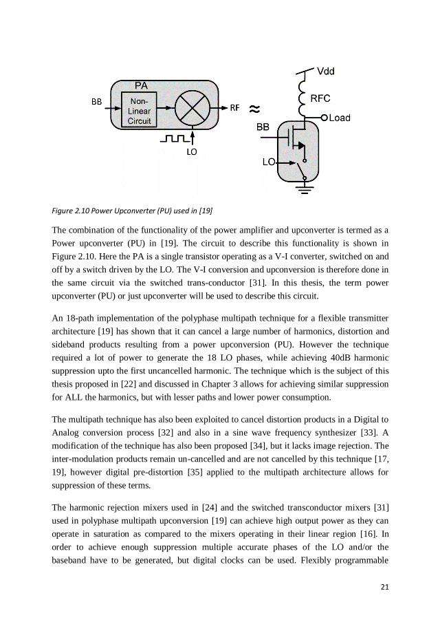
Figure 2.10 Power Upconverter (PU) used in [19]
The combination of the functionality of the power amplifier and upconverter is termed as a
Power upconverter (PU) in [19]. The circuit to describe this functionality is shown in
Figure 2.10. Here the PA is a single transistor operating as a V-I converter, switched on and
off by a switch driven by the LO. The V-I conversion and upconversion is therefore done in
the same circuit via the switched trans-conductor [31]. In this thesis, the term power
upconverter (PU) or just upconverter will be used to describe this circuit.
An 18-path implementation of the polyphase multipath technique for a flexible transmitter
architecture [19] has shown that it can cancel a large number of harmonics, distortion and
sideband products resulting from a power upconversion (PU). However the technique
required a lot of power to generate the 18 LO phases, while achieving 40dB harmonic
suppression upto the first uncancelled harmonic. The technique which is the subject of this
thesis proposed in [22] and discussed in Chapter 3 allows for achieving similar suppression
for ALL the harmonics, but with lesser paths and lower power consumption.
The multipath technique has also been exploited to cancel distortion products in a Digital to
Analog conversion process [32] and also in a sine wave frequency synthesizer [33]. A
modification of the technique has also been proposed [34], but it lacks image rejection. The
inter-modulation products remain un-cancelled and are not cancelled by this technique [17,
19], however digital pre-distortion [35] applied to the multipath architecture allows for
suppression of these terms.
The harmonic rejection mixers used in [24] and the switched transconductor mixers [31]
used in polyphase multipath upconversion [19] can achieve high output power as they can
operate in saturation as compared to the mixers operating in their linear region [16]. In
order to achieve enough suppression multiple accurate phases of the LO and/or the
baseband have to be generated, but digital clocks can be used. Flexibly programmable

22
digital frequency dividers can be exploited, enabling software defined and cognitive radios
to benefit from Moore’s law. Still, there are limits to the number of phases that can be
realized at high frequency, while phase accuracy and power dissipation is also a concern
[36, 37].
From the discussion above, we conclude that the multi-path mixer techniques exploiting
digital square-wave LO-paths have the most attractive properties for agile dynamic
spectrum access. In [24-26], harmonic rejection is achieved using different LO-phases and
amplitude weighting, sharing one baseband signal. If multiple baseband phases are also
generated, we can realize a Polyphase Multipath up-converter and now, not only harmonics
are cancelled, but also many distortion and side-band products [17, 19]. In other words:
apart from harmonic rejection mixing, linearity benefits are also achieved.
2.3 Cognitive Radio transmitter requirements
Regulators around the world are opening up the RF spectrum for devices that can operate
where-ever there is free spectrum available in a certain RF band [38, 39]. In order to meet
regulatory requirements it is crucial that these devices do not interfere with incumbent users
of the frequency spectrum. As shown in [40], one of the challenges for a cognitive radio
transmitter is that the out of band emissions (OOB) in the adjacent channels and beyond the
adjacent channels have to be less than 55dB and 53dB respectively relative to the desired
(maximum) signal power of 20dBm [38]. In terms of absolute power this means that the
OOB emissions should be ≤ -33dBm (5MHz signal bandwidth assumed as in [40]). If the
maximum signal power is in the range of 0-10dBm, which can be enough for a portable
device, the OOB emissions should then be 33dB-43dB (+10dBm-(-33dBm) = 43dB)
respectively below the desired signal. A more recent report from FCC [39] requires that out
of band emissions in the adjacent channel to be better than -38dBm (in 6 MHz), while the
maximum desired signal power specified is 17dBm. On a relative scale this requirement
implies that the out of band emissions should be 55dB below the desired signal. If the
signal to be transmitted has an output power of 0-10dBm, the OOB emission requirement
on a relative scale comes out to be 38dB-48dB (+10dBm-(-38dBm) = 48dB) respectively
below the desired signal. In essence if the output power to be transmitted is less, the OOB
emission requirements can also be reduced from their maximum values. At the maximum
output power levels the OOB requirements are also the toughest.

23
2.4 Conclusions
In literature there are many transmitter architectures which are focused towards multimode
or multi-standard operation for a SDR/ Cognitive radio Transmitter. Most of them focus on
making the baseband design flexible, relaxing or removing the baseband filtering,
improving the linearity and/or noise performance of the transmitter. A few of the
transmitter architectures focus on removing or suppressing the transmitted signals at and
around the harmonics of the local oscillator. The harmonic rejection mixer technique,
which requires multiphase LO along with amplitude weighting of one of the paths has
attractive properties for LO harmonic cancellation but doesn’t have distortion cancellation
properties. However, if multiple baseband phases are also generated along with a
multiphase LO, linearity benefits are also achieved as is the case with the Polyphase
Multipath Upconversion. This can be very beneficial in a dynamic spectrum access
environment. From the FCC reports on spectrum utilization for the unlicensed devices in
the TV bands, it is seen that that the out of band emission in the 6 MHz bandwidth are
required to be 55dB below the desired signal. The out of band emission requirement is
relaxed if the output power requirement is reduced.
References
[1] P. Eloranta, P. Seppinen, S. Kallioinen, T. Saarela, and A. Parssinen, "A Multimode Transmitter in 0.13 um CMOS Using Direct-Digital RF Modulator," Solid-State Circuits, IEEE Journal of, vol. 42, pp. 2774-2784, Dec 2007.
[2] X. He, J. van Sinderen, and R. Rutten, "A 45nm WCDMA Transmitter Using Direct Quadrature Voltage Modulator with High Oversampling Digital Front-End," in International Solid State Circuits Conference, 2010.
[3] S. M. Taleie, Y. Han, T. Copani, B. Bakkaloglu, and S. Kiaei, "A 0.18um CMOS Fully Integrated RFDAC and VGA for WCDMA Transmitters," in IEEE Radio Frequency Integrated circuits (RFIC) Symposium, 2008.
[4] W. M. Gaber, P. Wambacq, J. Craninckx, and M. Ingels, "A CMOS IQ direct digital RF modulator with embedded RF FIR-based quantization noise filter," in ESSCIRC (ESSCIRC), 2011 Proceedings of the, 2011, pp. 139-142.
[5] S. Fukuda, S. Miya, M. Io, K. Hamashita, and B. Nauta, "Direct-Digital modulation (DIDIMO) Transmitter with -156dBc/Hz Rx-Band Noise using

24
FIR structure," in Proc. European Solid-State Circuits Conf. (ESSCIRC), 2012, pp. 53-56.
[6] N. Ghittori, A. Vigna, P. Malcovati, S. D'Amico, and A. Baschirotto, "1.2-V Low-Power Multi-Mode DAC+Filter Blocks for Reconfigurable (WLAN/UMTS, WLAN/Bluetooth) Transmitters," Solid-State Circuits, IEEE Journal of, vol. 41, pp. 1970-1982, Sep. 2006.
[7] Z. Boos, A. Menkhoff, F. Kuttner, M. Schimper, J. Moreira, H. Geltinger, et al., "A fully digital multimode polar transmitter employing 17b RF DAC in 3G mode," in Solid-State Circuits Conference Digest of Technical Papers (ISSCC), 2011 IEEE International, 2011, pp. 376-378.
[8] Q. Huang, J. Rogin, X. Chen, D. Tschopp, T. Burger, T. Christen, et al., "A tri-band SAW-less WCDMA/HSPA RF CMOS transceiver with on-chip DC-DC converter connectable to battery," in Solid-State Circuits Conference Digest of Technical Papers (ISSCC), 2010 IEEE International, 2010.
[9] X. He and J. V. Sinderen, "A Low-Power, Low-EVM, SAW-Less WCDMA Transmitter Using Direct Quadrature Voltage Modulation," Solid-State Circuits, IEEE Journal of, vol. 44, pp. 3448-3458, Dec. 2009.
[10] M. Ingels, V. Giannini, J. Borremans, G. Mandal, B. Debaillie, P. Van Wesemael, et al., "A 5mm2 40nm LP CMOS 0.1-to-3GHz multistandard transceiver," in Solid-State Circuits Conference Digest of Technical Papers (ISSCC), 2010 IEEE International, 2010.
[11] R. B. Staszewski, J. L. Wallberg, S. Rezeq, C.-M. Hung, O. E. Eliezer, S. K. Vemulapalli, et al., "All-digital PLL and transmitter for mobile phones," Solid-State Circuits, IEEE Journal of, vol. 40, pp. 2469-2482, Dec. 2005.
[12] J. Mehta, R. B. Staszewski, O. Eliezer, S. Rezeq, K. Waheed, M. Entezari, et al., "A 0.8mm2 all-digital SAW-less polar transmitter in 65nm EDGE SoC," in Solid-State Circuits Conference Digest of Technical Papers (ISSCC), 2010 IEEE International, 2010, pp. 58-59.
[13] M. S. Alavi, R. B. Staszewski, L. C. N. de Vreede, and J. R. Long, "A Wideband 2 × 13-bit All-Digital I/Q RF-DAC," Microwave Theory and Techniques, IEEE Transactions on, vol. 62, pp. 732-752, Apr. 2014.
[14] A. Jerng and C. G. Sodini, "A Wideband Digital-RF Modulator for High Data Rate Transmitters," Solid-State Circuits, IEEE Journal of, vol. 42, pp. 1710-1722, Aug 2007.
[15] G. Cafaro, T. Gradishar, J. Heck, S. Machan, G. Nagaraj, S. Olson, et al., "A 100 MHz – 2.5 GHz Direct Conversion CMOS Transceiver for SDR Applications," in Radio Frequency Inegrated Circuits (RFIC) Symposium, 2007.
[16] M. A. F. Borremans, C. R. C. De Ranter, and M. S. J. Steyaert, "A CMOS dual-channel, 100-MHz to 1.1-GHz transmitter for cable applications," Solid-State Circuits, IEEE Journal of, vol. 34, pp. 1904-1913, 1999.

25
[17] E. Mensink, E. A. M. Klumperink, and B. Nauta, "Distortion cancellation by polyphase multipath circuits," IEEE Trans. Circuits Syst. II, Exp. Briefs, vol. 57, pp. 1785-1794, Sep. 2005.
[18] E. Mensink, E. A. M. Klumperink, and B. Nauta, "Distortion cancellation via polyphase multipath circuits," in Circuits and Systems, 2004. ISCAS '04. Proceedings of the 2004 International Symposium on, 2004, pp. I-1098-101 Vol.1.
[19] R. Shrestha, E. A. M. Klumperink, E. Mensink, G. J. M. Wienk, and B. Nauta, "A Polyphase Multipath Technique for Software-Defined Radio Transmitters," Solid-State Circuits, IEEE Journal of, vol. 41, pp. 2681-2692, 2006.
[20] E. Klumperink, R. Shrestha, E. Mensink, G. Wienk, Z. Ru, and N. Bram, "Multipath Polyphase Circuits and their Application to RF Transceivers," in Circuits and Systems, 2007. ISCAS 2007. IEEE International Symposium on, 2007, pp. 273-276.
[21] E. A. M. Klumperink, R. Shrestha, E. Mensink, V. J. Arkesteijn, and B. Nauta, "Cognitive radios for dynamic spectrum access - polyphase multipath radio circuits for dynamic spectrum access," Communications Magazine, IEEE, vol. 45, pp. 104-112, 2007.
[22] S. Subhan, E. A. M. Klumperink, and B. Nauta, "Towards suppression of all harmonics in a polyphase multipath transmitter," in Circuits and Systems (ISCAS), 2011 IEEE International Symposium on, 2011, pp. 2185-2188.
[23] S. Subhan, E. A. M. Klumperink, A. Ghaffari, G. J. M. Wienk, and B. Nauta, "A 100–800 MHz 8-Path Polyphase Transmitter With Mixer Duty-Cycle Control Achieving < -40 dBc for ALL Harmonics," Solid-State Circuits, IEEE Journal of, vol. 49, pp. 595-607, Mar. 2014.
[24] J. A. Weldon, R. S. Narayanaswami, J. C. Rudell, L. Li, M. Otsuka, S. Dedieu, et al., "A 1.75-GHz highly integrated narrow-band CMOS transmitter with harmonic-rejection mixers," Solid-State Circuits, IEEE Journal of, vol. 36, pp. 2003-2015, Dec. 2001.
[25] K. Jongsik, L. Seung Jun, K. Seungsoo, H. Jong Ok, E. Yun Seong, and S. Hyunchol, "A 54-862-MHz CMOS Transceiver for TV-Band White-Space Device Applications," Microwave Theory and Techniques, IEEE Transactions on, vol. 59, pp. 966-977, 2011.
[26] K. Un, M. P., and R. P. Martins, "A 53-to-75-mW, 59.3-dB HRR, TV-Band White-Space Transmitter Using a Low-Frequency Reference LO in 65-nm CMOS," Solid-State Circuits, IEEE Journal of, vol. 48, pp. 2078-2089, Sep 2013.
[27] R. Bagheri, A. Mirzaei, M. E. Heidari, S. Chehrazi, L. Minjae, M. Mikhemar, et al., "An 800-MHz-6-GHz Software-Defined Wireless Receiver in 90-nm

26
CMOS," Solid-State Circuits, IEEE Journal of, vol. 41, pp. 2860-2876, Dec.2006.
[28] S. Lerstaveesin, M. Gupta, D. Kang, and B.-S. Song, "A 48-860 MHz CMOS Low -IF Direct-Conversion DTV Tuner," Solid-State Circuits, IEEE Journal of, vol. 43, pp. 2013-2024, Sep. 2008.
[29] F. Gatta, R. Gomez, Y. J. Shin, T. Hayashi, and et.al, "An Embedded 65 nm CMOS Baseband IQ 48 MHz-1 GHz Dual Tuner for DOCSIS 3.0," Solid-State Circuits, IEEE Journal of, vol. 44, pp. 3511-3525, Dec. 2009.
[30] Z. Ru, N. A. Moseley, E. Klumperink, and B. Nauta, "Digitally Enhanced Software-Defined Radio Receiver Robust to Out-of-Band Interference," Solid-State Circuits, IEEE Journal of, vol. 44, pp. 3359-3375, 2009.
[31] E. A. M. Klumperink, S. M. Louwsma, G. J. M. Wienk, and B. Nauta, "A CMOS switched transconductor mixer," Solid-State Circuits, IEEE Journal of, vol. 39, pp. 1231-1240, 2004.
[32] G. L. Radulov, P. J. Quinn, P. Harpe, H. Hegt, and A. Van Roermund, "Parallel current-steering D/A Converters for Flexibility and Smartness," in Circuits and Systems, 2007. ISCAS 2007. IEEE International Symposium on, 2007, pp. 1465-1468.
[33] W. A. Ling and P. P. Sotiriadis, "A Nearly All-Digital Frequency Mixer Based on Nonlinear Digital-to-Analog Conversion and Intermodulation Cancellation," Circuits and Systems I: Regular Papers, IEEE Transactions on, vol. 58, pp. 1695-1704, 2011.
[34] E. A. Sobhy and S. Hoyos, "A Multiphase Multipath Technique With Digital Phase Shifters for Harmonic Distortion Cancellation," Circuits and Systems II: Express Briefs, IEEE Transactions on, vol. 57, pp. 921-925, 2010.
[35] Y. Xi, D. Chaillot, P. Roblin, L. Wan-Rone, L. Jongsoo, P. Hyo-Dal, et al., "Poly-Harmonic Modeling and Predistortion Linearization for Software-Defined Radio Upconverters," Microwave Theory and Techniques, IEEE Transactions on, vol. 58, pp. 2125-2133, 2010.
[36] X. Gao, B. Nauta, and E. A. M. Klumperink, "Advantages of Shift Registers Over DLLs for Flexible Low Jitter Multiphase Clock Generation," Circuits and Systems II: Express Briefs, IEEE Transactions on, vol. 55, pp. 244-248, 2008.
[37] E. Klumperink, R. Dutta, R. Zhiyu, B. Nauta, and X. Gao, "Jitter-Power minimization of digital frequency synthesis architectures," in Circuits and Systems (ISCAS), 2011 IEEE International Symposium on, 2011, pp. 165-168.
[38] FCC, "Second Report and Order and Memorandum Opinion and Order In the Matter of Unlicensed Operation in the TV Broadcast Bands, Additional Spectrum for Unlicensed Devices Below 900 MHz and in the 3 GHz Band," Nov. 2008.

27
[39] FCC, "In the Matter of Unlicensed Operation in the TV Broadcast Bands Additional Spectrum for Unlicensed Devices Below 900MHz and in the 3GHz Band," Sep. 2010.
[40] S. J. Shellhammer, A. K. Sadek, and W. Zhang, "Technical Challenges for Cognitive Radio in the TV White Space Spectrum," in Information Theory and Applications Workshop, 2009.

28
29
CHAPTER THREE
3 Polyphase Multipath Transmitter System Design
(section 3.1 and some part of section 3.2 of this chapter are taken from the author’s paper
[1] published in the proceedings of the International Symposium on Circuits and Systems
(ISCAS). Some part of Section 3.3, 3.4 and section 3.5 are taken from the author’s paper
published in the IEEE Journal of Solid State Circuits [2)]).
In chapter 2 some of the flexible transmitter architectures were briefly discussed. Among
these was the polyphase multipath upconversion architecture. In this chapter an
improvement in the polyphase multipath upconversion is discussed which allows to reduce
the number of polyphase paths in comparison to [3], while aiming to suppress ALL the
local oscillator (LO) harmonics. The aim is to achieve as high harmonic suppression as
possible while keeping the number of paths low. In section 3.1 an analysis of the choices
made in the 18-path upconverter are discussed. In section 3.2, the motivation for selecting a
particular duty cycle of the LO which led to the choice of an 8-path upconversion is
discussed. An analysis discussing the effects of LO duty cycle on the efficiency of the
upconverter is presented in section 3.3, while the multiphase LO generation and phase
mismatch issues are discussed in section 3.4 and section 3.5 respectively.
3.1 Poly-phase Multipath System Analysis
As discussed in section 2.2.1 and in [3], some of the up-converted terms in the
implementation of the polyphase multipath up-converter are not cancelled. Taking ωBB as
the input baseband signal and ωLO as the LO signal, the most dominant of these un-
cancelled terms in the output spectrum occurs at 3ωLO+3ωBB as discussed in [3] and shown
in Figure 3.1 for an 18-path Upconversion. The 3ωBB term (in the 3ωLO+3ωBB upconverted
spectral component) is the 3rd order distortion of the baseband signal, and can be reduced
by making the baseband section sufficiently linear or by using digital pre-distortion [4].
If differential baseband and differential LO signals are used and initially assuming that the
component at 3ωLO+3ωBB1 is not dominant, then the first dominant un-cancelled harmonic in
an N path PU occurs at N-1[3] times the LO frequency. The magnitude of this harmonic
1 This term can also be reduced by making the duty cycle of the LO=1/3.

30
decreases as N increases, as shown in Figure 3.2. Even with N=30 the harmonic suppression
does not reach -30dBc, while many parallel paths are needed. In the next section we explore
options to achieve <-40dBc harmonic suppression by a limited number of paths in
combination with simple RC filtering. This is relevant to reduce complexity, as an N-path
polyphase Transmitter also requires N Digital to Analog functions in parallel and N
reconstruction filter functions. Also the mixers require multiphase clocks and multiphase
analog baseband signals to drive them. Multiphase LO-generation becomes more
challenging as the number of paths increase, and will require a higher frequency if dividers
are used for flexible multiphase LO-generation.
Figure 3.1 .Output Spectrum for an 18-path Upconversion of a single tone[3]
Apart from the LO-phase, duty cycle is another degree of design freedom for LO-
generation. In [3] the duty cycle (D) of the LO was made 1/3 to suppress the 3rd LO
harmonic. This was done to reduce the 3ωLO+3ωBB term which is not cancelled by the
multipath architecture, as equation (2.5) in chapter 2 is satisfied for m=3 and j=0. The
magnitude of the 3ωLO+3ωBB term relative to the fundamental can be calculated by the
relation (Ap2 × a3 / 3 × 4a1) [5], assuming D=1/2, where a3 and a1 are the coefficients of the
nonlinearity as described by a Taylor approximation [6] and Ap is the amplitude of the input
sinusoid. Assuming Ap to be around 200mV, a3/a1 ≈ 3V-2, this term can be around -40dBc
for a switched transconductor PU as described in [3]. If some source degeneration is
applied for linearization or some RC-filtering is added at the output, this would make this
term even lower. So making D=1/3 is not essential in achieving -40dBc suppression of the
3ωLO+3ωBB term. Due to mismatches and phase inaccuracies, achieving much better
harmonic rejection than -40dBc is difficult [3]. Moreover a filter is still needed to reject the
first non-cancelled harmonic, which is discussed in the next subsection.

31
Figure 3.2. Magnitude of the N-1th Harmonic in an N path Transmitter driven by poly-phase 50% duty cycle ideal square-wave LO-signals [1].
3.1.1 Multipath System with a First order RC filter at the output.
It would be interesting to see how much suppression can be achieved if a first order tunable
RC low pass filter is placed at the output of a multipath upconverter. This is interesting
because in some cases the inherent parasitic capacitances at the output of the upconverter in
combination with the antenna load impedance can already provide a first order roll off.
Also it is relatively simple to make a bank of switchable capacitors on chip (to achieve
tunable first order filtering). The total suppression of the LO harmonics in such a case
would be a combination of the suppression due to the multipath system and the RC filter.
Assuming that the -3dB corner frequency of such an RC filter is placed such that the signal
loss for the desired 1st harmonic is ≤ 1dB, then the magnitude of the filter response as a
function of the first uncancelled harmonic (N-1th) in an N-path upconversion is shown in
Figure 3.3. The roll-off of Figure 3.2 expressed in terms of the N-1th harmonic (where N is
variable) is also shown. In essence some signal power would be lost for the sake of simpler
filtering and a large tuning range (cut-off frequency inversely proportional to C). The signal
loss can be avoided by the method to be discussed in section 3.2.1 (Case 2).
Adding the suppression, we can achieve <-40dBc combining multipath upconversion and
simple RC filtering if a ≥15th harmonic is the first un-cancelled harmonic, implying N≥ 16.
So if only a first order filter is used at the output of a multipath system, then sixteen or
more paths would be needed to suppress the harmonics to more than 40 dB. This is the case
when the duty cycle D=1/2.

32
Figure 3.3 Suppression due to 1st order RC at the (N-1)th harmonic(N is variable) , suppression due to the polyphase multipath upconversion with 50% duty cycle ideal square-wave also shown [1].
Since the duty cycle of the local oscillator (LO) is a degree of freedom in the harmonic
suppression, in the next section we see the benefit of varying the LO duty cycle, to achieve
harmonic suppression with less number of paths.
3.2 Eight Path Transmitter
It is possible to achieve harmonic suppression by varying the duty cycle D of the LO in a
multipath architecture. If we keep N even, a 180 degrees shifted version of the LO phase is
always available (e.g. for N = 4, phase = 0°, 90°, 180°, 270°), allowing for the suppression
of all the even order harmonics. This is desired as the 2nd harmonic becomes dominant
when D ≠ ½.
It is preferred to keep N as low as possible for complexity and power efficiency reasons,
while aiming for high harmonic suppression (40 to 50dBc as discussed in Section 2.3). In a
4-path architecture, also referred to as an IQ or image reject mixer, the first few un-
cancelled harmonics occur around the 3rd, 5th ,7th harmonic of the LO whereas in a 6-path
design they occur around the 5th ,7th,11th harmonic of the LO (see equation (2.5) in chapter
2)). The magnitude of these harmonics is much stronger than -40dBc as seen in Figure 3.2,
and requires significant filtering.
An 8-path design [1] presents the opportunity to suppress the two dominant harmonics (7th
and 9th) simultaneously, while allowing the next two harmonics (15th and 17th) to be distant
enough for simple 1st order RC filtering. This can be done by varying the duty cycle D of
the LO. The strength of the 7th and 9th LO harmonics for D=1/2 is -16.9dBc and -19dBc
respectively. This can be calculated by taking the magnitude of the Fourier series

33
coefficients (an and bn) of the LO waveform shown in Figure 3.4a.These coefficients and
the amplitude of the nth harmonic Vn are:
0
2( )cos( ) sin(2 )
T
n
Aa x t n t dt n D
T n
(3.1)
0
2( )sin( ) (cos(2 ) 1)
T
n
Ab x t n t dt n D
T n
(3.2)
2 2 2 2cos(2 )n n n
AV a b n D
n
(3.3)
Equation (3.3) is plotted as a function of D in Figure 3.4b, where the desired signal is
normalized to 0dBc for D=0.5. In the figure it can be seen that both the 7th and 9th LO
harmonic are at a level of around -31dBc when D is either ~7/16 or ~9/16. These are the
only two points in the Figure 3.4b where both the 7th and 9th harmonic components are
below -31dBc simultaneously [1]. Evaluating equation (3.3) in Table 3.1 we find an
optimum duty-cycle of 0.4365 (43.65%) to achieve simultaneous rejection for both V7 and
V9 to -31.9dBc compared to the fundamental at 43.65 % duty cycle. The conversion gain
for the fundamental is -4.1dB, only slightly worse than the -3.9 dB (2/ ) for 50% duty-
cycle. The optimum is close to D= 7/16 (43.75%) [1], where we find -30.9dBc and -33dBc
for the 7th and 9th harmonic. The reason for specifying the LO duty cycle D in a fractional
form is related to the way it is often generated using digital dividers as discussed in section
3.4. Comparing the results, we see that the optimum is rather sensitive: a duty-cycle change
of 0.1% from the optimum renders 1dB worse rejection. The variation in the 9th harmonic is
less of an issue as higher harmonics will undergo more attenuation by low-pass filtering. In
section 5.3 on duty cycle control, the circuit design used to keep variations in duty cycle <
0.1% is discussed.
Table 3.1 shows an improvement in harmonic suppression of at least 13 dB as compared to
the case when D=1/2. As the 7th harmonic is more than 2 octaves from the fundamental, a
simple first order filter can implement the missing 10dB to achieve <-40dBc (2 octaves
2x6dB=12dB filtering). The next two most dominant harmonics for an 8-path transmitter
occur at 15 and 17 times the LO, which are at a level of around -24dBc. A first order filter
can have around 20dB suppression there, which again brings the result at < -40dBc. Higher
harmonics are at an even lower amplitude level. One might wonder what happens for fewer
paths. A 4-path design is the minimum even-N design with image rejection, required for
single sideband transmission. In order to allow all the harmonics to be <-40dBc, the 3rd,
5th…13th harmonic would need to be significantly suppressed simultaneously, which is not
possible with any single D value.

34
Figure 3.4 (a) Square wave with duty cycle D (b) LO Harmonic content as a function of D.
Table 3.1 Harmonic Strength versus duty cycle
Duty Cycle V1 (dB) V2 (dB) V7 (dB) V9 (dB)
50.00% -3.922 -121.466 -20.824 -23.007
43.55% -4.101 -18.027 -37.200 -35.040
43.60% -4.099 -18.091 -36.600 -35.530
43.65% -4.096 -18.155 -36.039 -36.050
43.70% -4.093 -18.220 -35.514 -36.606
43.75% (7/16) -4.090 -18.286 -35.02 -37.202
43.80% -4.088 -18.352 -34.553 -37.843

35
Figure 3.5 (a) Output Network of multipath PU. (b) Single ended BPF circuit driven by a current source.
A similar argument can be given for not choosing 6 paths. Therefore the next even N of 8 is
chosen.
3.2.1 Eight path Transmitter and tunable RF Filter
The output network of a multipath Upconverter can be implemented as shown in Figure
3.5a, where Io represents the mixer output current and RL the (antenna) load impedance. The
presence of an inductor [3] allows the output node to be biased at VDD and therefore allows
for high output voltage swings around VDD, which is desired for high output power. If the
capacitors values C are tunable and the inductor value L is kept fixed, it is possible to realize
a tunable band-pass filter (BPF) response.
For simplicity, consider the single ended (half-circuit) version of the output network
driven by a current source as shown in Figure 3.5b. The Q of the parallel RLC network is
approximately given by:
L
CQ R
L
(3.4)
For low Q value (<<1), the inductor value is big (L >> R2C), and for a high Q (≥ 1), the
inductor value is small (L ≤ R2C).
For briefness and convenience, in this section big L and small L refer to this range of L
values. A big L results in broadband behavior, and a small L in narrowband BPF behavior
around the LC resonance frequency (see Figure 3.6).

36
Suppression 6dB/Octave
Figure 3.6 Tunable BPF response [1].
Above resonance, RC filtering dominates ultimately resulting in a roll-off of 6dB/octave as
shown in Figure 3.6. Closer to resonance, the roll-off can be either lower (Big L, low-Q
case) or higher (Small L case with high-Q peaking behavior). This in part also depends on
how the inductors are implemented due to losses in the coils. Certainly at low frequencies
below 1GHz, on-chip coils are big and have rather low Q. It is typically preferred to use
off-chip high-Q coils. In this section we consider two cases, the first case with two big
inductors L, often referred to as “RF chokes” resulting in a low Q RLC network, the other
with two smaller inductors allowing for peaking in the filter response resulting in a high Q
RLC network.
Case 1: Low Q RLC network (big L)
When the inductor value is big, the filtering is mainly due to the RC filter network. The
harmonic suppression of such a filter is the same as shown in Figure 3.3. To have the filter
cover a wide frequency range for the fundamental the capacitor value needs to be tunable.
In order to determine the range of values of the capacitor, we again consider the single
ended case as shown in Figure 3.5b. The C value can be given as:
C
(3.5)
where fc is at the second harmonic (2×ωLO) to keep the desired signal loss ≤ 1dB. For a
frequency range of 100-800 MHz and assuming (single ended) RL /2=50Ω, then at the
lowest frequency the C value should be 16pf and at the higher end it should be 2pf. These
values are small enough to be implemented on chip. It can be seen also that the cut off

37
frequency is inversely proportional to the C value. The suppression achievable with such an
RC filter is given in Table 3.2.
Figure 3.7 Difference in harmonic suppression of RC and RLC filter
Case 2: High Q RLC network (small L)
In the first case the inductance of the filter did not play an active role in the filter behavior.
If more harmonic suppression is required then it can be useful to utilize small inductance
value instead of an RF choke. This results in a higher Q value (≥1) and can provide at least
6dB improvement in the suppression of higher harmonics as compared to the first case.
This is because in the low Q RLC (or just RC) case the corner frequency is placed at 2×ωLO
to limit signal loss to 1dB, whereas in the high Q RLC case the desired signal is placed
almost at the LO frequency so higher harmonics undergo more attenuation as shown in
Figure 3.7. In the figure the desired frequency component at 800 MHz undergoes 1dB more
attenuation for the RC case and the undesired 7th harmonic at 5.6 GHz undergoes 5 dB
more suppression for the RLC network case therefore in total 6 dB better harmonic
suppression is achieved for the RLC case. Similar to the first case the inductors are
assumed to be off chip and have low loss. The Q of the parallel RLC network is
approximately given by:
0
LRQ
L
(3.6)
The Q of the filter for a fixed RL and L decreases with higher resonance frequencies ω0.
Therefore we define the suppression for the highest frequency covered by the LO, so that
for all the lower frequencies the filter would have higher Q and hence higher suppression. If
we assume that at the highest LO frequency the Q=1, then we can place the upconverted

38
signal at the resonance frequency of the filter and get roughly 6dB/octave suppression of
the higher harmonics. Ideally there is no loss of the upconverted signal, which implies
better efficiency as compared to the first case. Interestingly each doubling of the Q also
gives roughly 6dB of additional suppression as can be observed in Figure 3.8, due to the
peaking behavior.
Figure 3.8 6dB higher suppression (shown at the 7th harmonic) with doubling of Q, due to halving of ω0 in (3.6).
The (worst-case) suppression at the highest LO-frequency is shown in Figure 3.9 along
with the RC filter suppression shown in Figure 3.3. The figure shows the filter suppression
at different harmonics of the LO in the output spectrum. It can be seen that the RLC filter
has 6dB better suppression for higher harmonics as compared to the RC (RLC with Q<<1)
filter. Using eq. (3.6), the inductor value needed to achieve a Q=1 at 800MHz is 10nH. The
C value required at this resonance frequency is 3.95pf and at 100MHz it is 32pf. An
inductor of 10nH may be small enough to be considered for implementation on chip, but
the associated losses will degrade efficiency.
As the antenna is off-chip anyway for these frequencies, off-chip coils are probably
preferred. Also, if more power is needed than given the voltage breakdown conditions of a
power up-converter (PU) chip, adding a transformer is an option. To summarize, the
amplitude of the dominant spectral components in various scenarios of an 8-path
transmitter are given in Table 3.2. It is important to note here that the tuning range in case
of an RC filter is proportional to 1/C while in the RLC case it is proportional to 1/√C. So
although the High Q RLC is good for harmonic rejection, its tuning range is less than the
RC (Low Q RLC) filter for a given range of C values. On the other hand the RC filter gives
loss but has better tuning range. So both approaches have their value.

39
Figure 3.9 Suppression with RLC filter (Q=1) and 1st order RC Filter (corner frequency at 2nd harmonic)
Table 3.2 Harmonic Magnitude in an 8-path Transmitter
Spectral
components
3ωLO+3ωBB
(dBc)
7ωLO-ωBB
(dBc)
9ωLO+ωBB
(dBc)
15ωLO-ωBB
(dBc)
17ωLO+ωBB
(dBc)
1 50% Duty
Cycle <-38 -17 -19 -24 -25
2 ~7/16 Duty
Cycle <-40 -32 -32 -24 -25
3 RC with
fc=2×ωLO -4 -11 -13 -17 -19
4 RLC with
Q=1 -9 -17 -19 -23 25
5 Total
Suppression
[2+3]
<-44 -43 -45 -41 -44
6 Total
Suppression
[2+4]
<-49 -49 -51 -47 -50
40
3.3 Efficiency vs. duty cycle
We have seen in Section 3.2 that for harmonic suppression a duty cycle of 43.65 % is
preferred. As power efficiency is a concern for a Power Upconverter [3], we will in this
section analyze the duty cycle ratio which provides the optimal power efficiency. In the
analysis we assume that the mixers used for upconversion are switched gm mixers [7],
where a transconductor is switched on and off by a switch. We consider the single ended2
PU using switched gm3 multipath mixers directly driving the load RL as shown in Figure
3.10.
The mixer efficiency is defined as:
rf desired
dc
P
P
(3.7)
Where Prf-desired is the desired up-converted signal power delivered to the load and Pdc is the
dc power consumed in the mixer.
For simplicity we first assume ideal and perfectly linear transconductors with a large-signal
V-I conversion (Gm) equal to its small-signal gm and ideal switches. The single tone
baseband signal applied at the input of the gm blocks can be given as:
(3.8)
Where Vgto is the dc bias voltage (e.g. the overdrive voltage of a MOSFET above threshold
(Vth). Vp is the baseband amplitude voltage, which should not exceed Vgto to avoid
clipping4.
The dc power consumed in N path mixer can be given by:
dc dd dcP V I (3.9)
2Single ended is assumed for simplicity in analysis, in the implemented upconverter (chapter 5) the output
power is taken differentially. 3It is assumed that no current flows through the gm block when the LO switch is off.
4 Although ideal V-I conversion is assumed but clipping would occur in practical circuits.
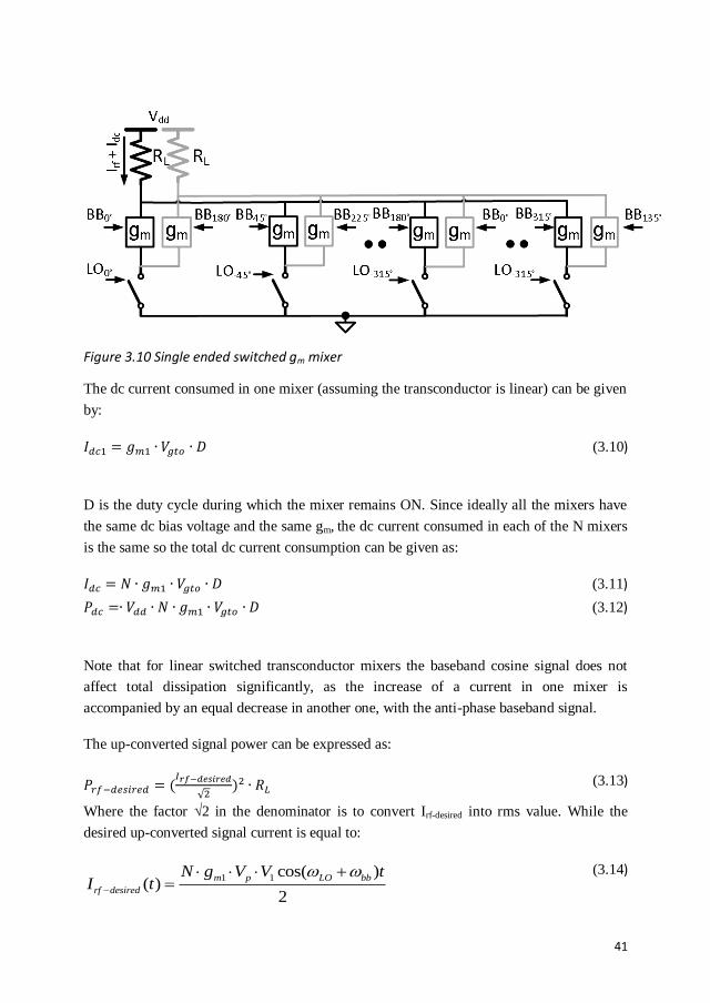
41
Figure 3.10 Single ended switched gm mixer
The dc current consumed in one mixer (assuming the transconductor is linear) can be given
by:
(3.10)
D is the duty cycle during which the mixer remains ON. Since ideally all the mixers have
the same dc bias voltage and the same gm, the dc current consumed in each of the N mixers
is the same so the total dc current consumption can be given as:
(3.11)
(3.12)
Note that for linear switched transconductor mixers the baseband cosine signal does not
affect total dissipation significantly, as the increase of a current in one mixer is
accompanied by an equal decrease in another one, with the anti-phase baseband signal.
The up-converted signal power can be expressed as:
(3.13)
Where the factor √2 in the denominator is to convert Irf-desired into rms value. While the
desired up-converted signal current is equal to:
1 1 cos( )( )
2
m p LO bb
rf desired
N g V V tI t
(3.14)

42
Figure 3.11 Efficiency peaks at 37% Duty Cycle.
Where the factor 2 in the denominator is due to the product of two cosines (bb and LO), V1
is the amplitude of the fundamental harmonic of the LO as given in (3.3), for n=1 and A
replaced by the amplitude of the desired signal current. In all the paths the desired signal
has the same phase, therefore they add up constructively, which explains N in (3.14).
Substituting (3.3) in (3.14) and taking magnitude:
(3.15)
2 2 2
1
2
(2 2cos(2 ))P
8
m p
rf desired L
N g V DR
(3.16)
Figure 3.11 shows a plot of equation (3.7), (3.12) and (3.16) as a function of D, where the
following practical values were used: N=8, gm = 35mS, Vp =0.2,Vgto = 0.32, Vdd =1.5. The
efficiency curve, peaks at a duty cycle of around 0.37
The desired signal (Prf-desired) starts to decrease after D=0.5, while the DC power (Pdc)
continues to increase as shown in Figure 3.11, therefore intuitively the optimal point should
lie somewhere before that. In order to assess the validity of this very coarse model, circuit
simulations (using the mixers discussed in Section 5.5) in a standard 160nm CMOS process
are also shown in Figure 3.11. The predicted shape is roughly right, but with a shift. This
difference is mainly due to the assumption that one mixer path does not influence the other
and also assuming linear devices. Simulations done with different circuit parameters show
the optimum efficiency point lies in the range of D=0.25 and D=0.35. We conclude that the
targeted duty-cycle D=0.4365 lies between D=0.5 and the optimum efficiency point.
Although not exactly optimal, the power efficiency compared to D=0.50 is 10-20% better.

43
3.4 Generating LO Duty Cycle
An 8-path transmitter requires 8-phase LO signals to drive the mixer switches. The
LO phases can be generated by a divide-by-8 circuit [8]. For low phase mismatch it is
desired to drive all flip-flops (FF) in a divide-by-8 circuit by the same master clock. A
chain of 8 FF cells is needed to generate all the phases. It is possible to make the duty cycle
ratio k/8 (where k=1, 2…7), by using digital dividers [8], therefore a nice fraction of the
duty cycle is desired. However to make the duty cycle ratio 7/16 requires the
implementation of 8 additional FF cells (for divide by 16). This is possible but requires
extra power consumption and also limits the maximum output frequency in a particular
process technology, since the input frequency of the divider chain then has to be 16 times
higher than the LO frequency. Moreover, from Table 3.1 it is seen that it is actually better
for the 7th harmonic rejection to tune the duty-cycle to a slightly lower value than 7/16.
Since 0.4365 is rather close to 0.50, we use an 8-phase 50% duty-cycle clock generated by
a divide-by-4 circuit and delay the rising edge (only by a ratio of 0.063) to reduce duty-
cycle (see Figure 3.12). This low delay introduces a negligible phase noise degradation
compared to other sources of noise. A buffer afterwards can again make the edge steep. To
ensure a clean output spectrum, the harmonic content can be monitored and controlled by
adapting the duty-cycle. A cognitive radio transceiver would likely have a spectrum
analyzer on board [9-12]. The harmonics of the transmit frequency can be detected5 by the
spectrum analyzer provided they fall within the band of the analyzer, which is likely for
low transmit-frequencies, where the high harmonics are the most problematic. If the 7th or
9th harmonics are at a very high frequency outside the input frequency range of the
spectrum analyzer, detection will require additional techniques.
Figure 3.12 shows that starting from a duty cycle ratio of 1/2 the rising edge can be slowed
to reach the required ratio of ~7/16. This way the effective LO waveform has un-symmetric
rise and fall times but the effective time the mixer switch remains ON can be decreased,
thus approximating a 7/16 ratio. If the LO waveform switches between 0 and VDD and the
mixer switch turns on at VDD/2, the required edge delay as a ratio of the LO period is 1/8.
For a 1GHz LO, this means a rise time of 125ps.For a frequency agile transmitter making
the falling edge delayed by a ratio of 1/8 of the LO period over a wide
5 Spectrum sensing receivers should be very sensitive and able to measure very weak signal levels and with good
degree of accuracy. Even if currently such receivers are not available commercially, we think that this will change.
See for instance the performance numbers achieved in [9-12]. In this thesis we assume that detection of
problematic harmonic content is feasible and aim for duty-cycle tuning to control this problem.

44
Figure 3.12 Making D = 7/16 from D = 1/2
frequency range requires adding a tuning mechanism to the LO waveform. Such a tuning
mechanism will be discussed in Chapter 5 on duty cycle control.
3.5 Effect of Phase Mismatch
A mathematical analysis of the effect of mismatch on multi-path polyphase circuits can be
found in [13], providing an estimate of the Harmonic Rejection Ratio of cancelled (C)
harmonics as:
2
22 2 2 2
2
1
( 1) LO
N
N k ma
(3.17)
where E(HRRk,m) is the expected value for a tone resulting from the kth harmonic of the LO
and mth harmonic of the baseband signal. Pk,m,reference is the power before rejection, produced
by a single path transmitter, while Pk,m,rejected is the power after (imperfect) rejection by the
multipath technique due to the presence of mismatch.2
,2
,2
are the variances of
the stochastic variables (LO phase mismatch error), (BB phase mismatch error) and
(amplitude mismatch error), respectively. Note that a higher number of paths has a
positive effect on HRR. In order to find the effect of mismatch on the harmonics which are
not cancelled (index NC), a similar analysis is done, resulting in [2]:
(3.18)
Note that the expected value of this equation for small values of amplitude and phase
mismatch is very close to one. This is because the non-cancelled harmonics even in the
presence of mismatch almost fully add up in phase. In the measurement section in Chapter
5 we will observe this effect.

45
3.6 Conclusion
The analysis of a previous implementation of the polyphase multipath technique shows that
making the duty cycle of the LO 1/3 is not essential in achieving ≥ 40dB harmonic
suppression. Therefore the duty cycle of the LO could be made different than 1/3 to
suppress other dominant harmonics. It is shown that a lot of parallel paths are needed to
achieve high harmonic suppression. If the duty cycle is kept at 1/2, then ≥16 paths are
needed, to achieve 40 dB harmonic suppression in combination with a first order RF filter.
Making a 16 path polyphase upconverter can be complex and will consume a lot of power.
Therefore some other design option is required.
An 8-path polyphase transmitter has the two most dominant spectral products around the 7th
and 9th harmonic of the LO. It is shown that an 8-path polyphase transmitter with a duty
cycle of 43.65% can suppress both the 7th and 9th harmonic of the LO by more than 31dB
compared to the fundamental signal. If a 1st order RF filter is applied the overall rejection
becomes more than 40dB for all the harmonics. This can be improved by 6dB if a high Q
tunable RLC network is used at the output but at the cost of capacitor range. It could be
possible to achieve the required duty cycle by delaying the rising edge of the LO starting
from a duty cycle of 50% and reaching ~43.65%. The duty cycle ratio of 43.65% is better
than 50% in terms of power efficiency, while the non-cancelled harmonics even in the
presence of phase mismatch almost fully add up in phase.
References
[1] S. Subhan, E. A. M. Klumperink, and B. Nauta, "Towards suppression of all harmonics in a polyphase multipath transmitter," in Circuits and Systems (ISCAS), 2011 IEEE International Symposium on, 2011, pp. 2185-2188.
[2] S. Subhan, E. A. M. Klumperink, A. Ghaffari, G. J. M. Wienk, and B. Nauta, "A 100–800 MHz 8-Path Polyphase Transmitter With Mixer Duty-Cycle Control Achieving < -40 dBc for ALL Harmonics," Solid-State Circuits, IEEE Journal of, vol. 49, pp. 595-607, Mar. 2014.
[3] R. Shrestha, E. A. M. Klumperink, E. Mensink, G. J. M. Wienk, and B. Nauta, "A Polyphase Multipath Technique for Software-Defined Radio Transmitters," Solid-State Circuits, IEEE Journal of, vol. 41, pp. 2681-2692, 2006.
[4] Y. Xi, D. Chaillot, P. Roblin, L. Wan-Rone, L. Jongsoo, P. Hyo-Dal, et al., "Poly-Harmonic Modeling and Predistortion Linearization for Software-Defined Radio Upconverters," Microwave Theory and Techniques, IEEE Transactions on, vol. 58, pp. 2125-2133, 2010.

46
[5] B. Razavi, RF Microelectronics. Upper Saddle River, NJ: Prentice Hall, 1998. [6] E. Mensink, E. A. M. Klumperink, and B. Nauta, "Distortion cancellation by
polyphase multipath circuits," IEEE Trans. Circuits Syst. II, Exp. Briefs, vol. 57, pp. 1785-1794, Sep. 2005.
[7] E. A. M. Klumperink, S. M. Louwsma, G. J. M. Wienk, and B. Nauta, "A CMOS switched transconductor mixer," Solid-State Circuits, IEEE Journal of, vol. 39, pp. 1231-1240, 2004.
[8] Z. Ru, N. A. Moseley, E. Klumperink, and B. Nauta, "Digitally Enhanced Software-Defined Radio Receiver Robust to Out-of-Band Interference," Solid-State Circuits, IEEE Journal of, vol. 44, pp. 3359-3375, 2009.
[9] M. S. Oude Alink, E. A. M. Klumperink, A. B. J. Kokkeler, Z. Ru, W. Cheng, and B. Nauta, "Using Crosscorrelation to Mitigate Analog/RF Impairments for Integrated Spectrum Analyzers," Microwave Theory and Techniques, IEEE Transactions on, vol. PP, pp. 1-11, 2013.
[10] M. S. Oude Alink, E. A. M. Klumperink, A. B. J. Kokkeler, M. C. M. Soer, G. J. M. Smit, and B. Nauta, "A CMOS-Compatible Spectrum Analyzer for Cognitive Radio Exploiting Crosscorrelation to Improve Linearity and Noise Performance," Circuits and Systems I: Regular Papers, IEEE Transactions on, vol. 59, pp. 479-492, 2012.
[11] M. S. Oude Alink, E. A. M. Klumperink, M. C. M. Soer, A. B. J. Kokkeler, and B. Nauta, "A 50Mhz-To-1.5Ghz Cross-Correlation CMOS Spectrum Analyzer for Cognitive Radio with 89dB SFDR in 1Mhz RBW," in New Frontiers in Dynamic Spectrum, 2010 IEEE Symposium on, 2010, pp. 1-6.
[12] M. S. Oude Alink, A. B. J. Kokkeler, E. A. M. Klumperink, G. J. M. Smit, and B. Nauta, "Fast, Sensitive, Efficient, and High-SFDR Spectrum Sensing with Crosscorrelation Energy Detection," Journal on Emerging and Selected Topics on Circuits & Systems (JETCAS), on:"Advanced Circuits and Systems for CR/SDR Applicaions", Dec. 2013.
[13] E. Mensink, E. A. M. Klumperink, and B. Nauta, "Distortion cancellation via polyphase multipath circuits," in Circuits and Systems, 2004. ISCAS '04. Proceedings of the 2004 International Symposium on, 2004, pp. I-1098-101 Vol.1.

47
CHAPTER FOUR
4 Mixed-Signal System Design
This chapter deals with the mixed-signal multiphase baseband signal generation of the 8-
path up-converter presented in the previous chapter. The aim is to derive a set of
requirements and present feasible design directions. As discussed previously, the aim of the
complete transmitter is to have the local oscillator (LO) originated harmonics better than -
40dBc in the output spectrum. We aim to keep the harmonics originating from the baseband
paths much better than -40dBc and even aim for lower so that they do not become a
bottleneck.
The 8-path polyphase transmitter requires eight baseband paths to drive the 8-path mixers.
This could be realized in the digital domain by the weighted addition of two quadrature
baseband signals. The method to generate these multiphase baseband signals is presented
in section 4.1. The baseband signals require a certain DAC resolution to achieve <-50dBc
unwanted signal components. The resolution requirements of the Digital-to-Analog
Converter (DAC) are discussed in section 4.2.
A reconstruction filter is conventionally required after the DAC, to remove unwanted DAC
images and noise. In literature, multiple parallel DACs whose outputs are combined have
been shown to be beneficial in terms of DAC image cancellation. Techniques exploiting
multiple parallel DACs to cancel or suppress some of the DAC images in a multipath up
converter are discussed in section 4.3.
The DAC design should be such that the mismatch between the multiphase baseband paths
can be minimized. A possible solution is to share the voltage reference of a ladder DAC or
another possibility is to use one time-interleaved DAC. In section 4.4 these DACs are
discussed.
A technique to relax reconstruction filtering requirements is to use oversampling of the
digital data. The extra cost is area and power consumed in the digital domain. It is shown
that using an interpolation filter for oversampling is feasible and does not dominate the
overall power budget in the given technology node. The digital interpolation filter design
used for oversampling is presented in section 4.5.

48
4.1 Multiphase Baseband Generation
Before proceeding to discuss multiphase baseband generation, it is instructive to see the
characteristics of an ideal phase shifter and how it relates to an ideal time delay, since these
terms will be used in the text. As can be seen in Figure 4.1, the ideal phase shifter has a
constant phase over frequency while the ideal delay has a linear phase over frequency [1].
This behavior can only be approximated in practical circuits.
Figure 4.1. Ideal phase shifter (a) ideal time delay (b) (frequency and phase axis are linear)[1]
Figure 4.2. First set of phase shifts in digital.
One of the reasons why the poly-phase multipath technique is particularly suitable for a
transmitter is the possibility to exploit digital techniques in baseband to implement the first
set of phase shifts shown in Figure 4.2(see chapter 2/3). With the advancement in IC
technology more complex digital circuits can be made to approximate ideally wanted
behavior. The second set of phase shifters are implemented via (digital) LO-phase shifting

49
in analog mixers. In contrast, in a receiver the RF input would need to be phase shifted in
the analog domain which can be a challenge for wide fractional bandwidths[2].
In order to understand how the multiphase digital baseband signals can be generated, it is
instructive to understand how the multiphase transmitter relates to a conventional fully
analog single sideband transmitter[3]. For a Cognitive radio transmitter, spectral efficiency
is vital and it is obviously preferred to not transmit the same (redundant) information in
both the upper and lower sideband. Image rejection allows for realizing a single sideband
transmitter. We will analyze the image cancellation properties of the mixers here using
cosine and sine functions following [2],[3], and verify results by simulation using the same
signals.
Figure 4.3(a) Conventional Single sideband upconversion. (b) Up-converted spectrum occurs around the ωLO frequency.
Figure 4.3a shows the conventional single sideband transmitter architecture[3] and Figure
4.3b the resulting upconverted spectrum around the LO. The input cosine term is referred to
as I, while the input sine term is referred to as the Q signal. In mathematics:
(4.1)
(4.2)
(4.3)
(4.4)
Here the baseband signals with a phase difference of -90° among them appear on the high
side of the LO after upconversion while the baseband signals with a phase difference of

50
+90° among them appear on the low side of the LO after upconversion as seen from
(4.1),(4.2) and (4.4).
Often the A and B signals are implemented differentially (signals with 180° difference
between them as shown in Figure 4.4) to achieve even order distortion suppression. In
essence there are then 4 single ended baseband signals, or equivalently 2 differential
baseband signals as shown in Figure 4.4. It should be noted that A and B are part of one
baseband signal while after upconversion with an LO frequency their images (either upper
or lower sideband) are ideally cancelled after the summation. Ideally the image frequency
components as well as the LO signal are cancelled but in practice mismatches will lead to
incomplete cancellation. Note however that both the residual image and LO-signal fall
inside the transmitted signal band and do not interfere with other users of the spectrum,
which are out of that band.
Figure 4.4.Upconversion with two differential baseband signals to cancel even order distortion.
For an 8-path software defined radio/ cognitive radio transmitter, digital streams
corresponding to the A and B signals are needed. Not only differential A and B baseband
streams are required but also additional baseband phases. In order to generate the single
sideband up-converted spectrum as shown in Figure 4.3b, for an 8-path transmitter the
architecture of Figure 4.5 can be used. Four additional baseband phases are required
compared to the conventional upconverter in Figure 4.4. To generate the additional phase
shifted baseband streams, a weighted addition of the input A and B streams is used. This

51
can be accomplished in the digital domain via a vector modulator [4] architecture as shown
in Figure 4.6. The figure shows how to generate the 45 degree phase but the same principle
can be used to generate the 135 degree phase. It can be seen that the required phases can be
generated from the commonly used I/Q baseband data and without requiring additional
baseband inputs.
Figure 4.5.Multiphase baseband required for 8-path upconversion.

52
Figure 4.6. Fixed weighted vector addition to generate phase shifted baseband (only one of the 8-generated phases is shown).
Note that only fixed coefficients (1/√2) are required to generate the phase shifts halfway
between the I/Q signals. Two multiplications and one addition would be needed to
implement the vector modulator. If differential DAC’s are used then the 180 degrees shifted
version of the baseband signals can be generated also in the analog domain. Overall then
two additional differential DAC’s would be required as compared to a conventional IQ
transmitter.
A digital phase shifter architecture was synthesized in Cadence synthesis tool to generate
the 8 digital phase shifted baseband signals based on the vector modulator architecture
shown in Figure 4.6. The VHDL code of the design can be found in the APPENDIX B. In
160nm CMOS, it would consume an area of (0.01 mm2). It has 16-bit processing resolution
while having 8, 8-bit outputs (digital resolution will be discussed in section 4.2), running at
50MHz, and expected (pre-layout) power consumption of only 2.5mW. Compared to the
overall transmitter power and area (see benchmark Table in Chapter 5) of larger than
120mW and area of 0.1 mm2, this phase shifter architecture consumes much less power and
area.

53
4.2 DAC Resolution Impact on a Poly-phase Multipath
Transmitter
In the previous chapter it was shown that most of the harmonics produced due to non-
linearity in the PU design can be cancelled using the multipath principle. These harmonics
were cancelled on the assumption that analog signals are driving the mixers. When we
consider the digital baseband signals and their conversion to the analog domain,
quantization errors occurs which tend to produce harmonics of the baseband signal [5]. It
should be noted that as mentioned in [6], some authors refer to the quantization errors as
noise, however quantization errors show “in a limited sense noise properties” [6]. These
harmonics of the baseband signal would dominate the output spectrum for low resolution
digital to analog conversion in the absence of reconstruction filter. Possibly the multipath
technique might be an option to suppress these terms so that synergy between DAC and
upconverter design occurs. Several questions may arise, e.g.:
What would happen if digital signals are converted to an amplitude discrete
representation in the presence of the multipath technique?
For both single tone or multi-tone sinusoids, what effect does finite D/A resolution
have on the output of a multipath transmitter?
These questions are investigated first with the assumption that both sets of phase shifts
shown in Figure 4.7 are ideal (section 4.2.1). Then the scenario where the second set of
phase shifts are provided with mixers (having frequency translation) is investigated in
section 4.2.2.
4.2.1 Multipath Technique applied to a Uniform DAC with ideal Phase
Shifter
If a pure sinusoid is amplitude quantized in an ADC (resembling a stair-case), then uniform
quantization results in pure harmonic distortion [7], and the output spectrum shows
distortion terms (when sampled, these distortion components will alias, if their frequencies
are higher than Nyquist [7]) which are multiples of the fundamental frequency, especially
for low resolution [6]. The output spectrum of a Digital to Analog conversion with a digital
sine input with the same resolution would show the same distortion in the absence of
reconstruction filtering as in both cases the time domain signal is the same stair-case
approximation of a sine.
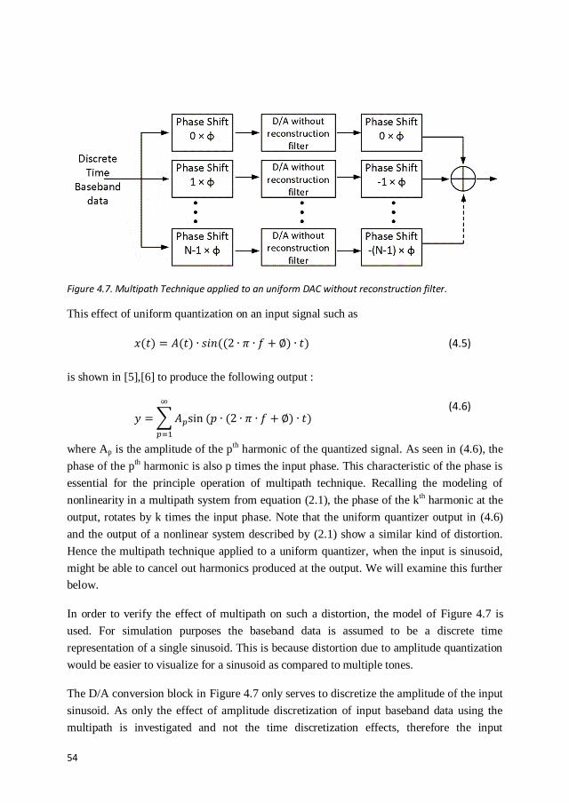
54
Figure 4.7. Multipath Technique applied to an uniform DAC without reconstruction filter.
This effect of uniform quantization on an input signal such as
(4.5)
is shown in [5],[6] to produce the following output :
(4.6)
where Ap is the amplitude of the pth harmonic of the quantized signal. As seen in (4.6), the
phase of the pth harmonic is also p times the input phase. This characteristic of the phase is
essential for the principle operation of multipath technique. Recalling the modeling of
nonlinearity in a multipath system from equation (2.1), the phase of the kth harmonic at the
output, rotates by k times the input phase. Note that the uniform quantizer output in (4.6)
and the output of a nonlinear system described by (2.1) show a similar kind of distortion.
Hence the multipath technique applied to a uniform quantizer, when the input is sinusoid,
might be able to cancel out harmonics produced at the output. We will examine this further
below.
In order to verify the effect of multipath on such a distortion, the model of Figure 4.7 is
used. For simulation purposes the baseband data is assumed to be a discrete time
representation of a single sinusoid. This is because distortion due to amplitude quantization
would be easier to visualize for a sinusoid as compared to multiple tones.
The D/A conversion block in Figure 4.7 only serves to discretize the amplitude of the input
sinusoid. As only the effect of amplitude discretization of input baseband data using the
multipath is investigated and not the time discretization effects, therefore the input
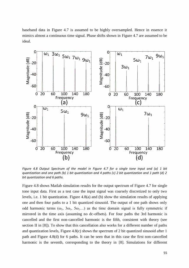
55
baseband data in Figure 4.7 is assumed to be highly oversampled. Hence in essence it
mimics almost a continuous time signal. Phase shifts shown in Figure 4.7 are assumed to be
ideal.
Figure 4.8 Output Spectrum of the model in Figure 4.7 for a single tone input and (a) 1 bit quantization and one path (b) 1 bit quantization and 4 paths (c) 2 bit quantization and 1 path (d) 2 bit quantization and 6 paths.
Figure 4.8 shows Matlab simulation results for the output spectrum of Figure 4.7 for single
tone input data. First as a test case the input signal was coarsely discretized to only two
levels, i.e. 1 bit quantization. Figure 4.8(a) and (b) show the simulation results of applying
one and then four paths to a 1 bit quantized sinusoid. The output of one path shows only
odd harmonic terms (ω1, 3ω1, 5ω1…) as the time domain signal is fully symmetric if
mirrored in the time axis (assuming no dc-offsets). For four paths the 3rd harmonic is
cancelled and the first non-cancelled harmonic is the fifth, consistent with theory (see
section II in [8]). To show that this cancellation also works for a different number of paths
and quantization levels, Figure 4.8(c) shows the spectrum of 2 bit quantized sinusoid after 1
path and Figure 4.8(d) for 6 paths. It can be seen that in this case the first non-cancelled
harmonic is the seventh, corresponding to the theory in [8]. Simulations for different

56
number of paths and various quantization levels confirm that the first non-cancelled
harmonic of the quantization process is the (n+1)th where n is the number of paths.
Figure 4.9.Output Spectrum of two tone applied to the model in Figure 4.7 (a) 1 bit quantized one path system (b) 1 bit quantized and 4 path system.
Simulations with two-tone inputs were also done to check correspondence with the theory
in [8]. For tones at ω1 and ω2, intermodulation products occurring at 2ω2-ω1, 2ω1-ω2, 3ω2-
2ω1, 3ω1-2ω2, …. are expected to remain uncancelled, and so are adjacent intermodulation
terms (separated by ω1-ω2) around . Figure 4.9(a) shows the spectrum of a 2-tone
signal applied to a 1 bit quantizer for 1 path and Figure 4.9(b) exploiting 4 paths. From the
figure it can be seen that with 4 paths, all terms are cancelled except for terms satisfying eq.
4 in [8]: p + q = j x n+1, where p and q are integer values. For n=4, the terms 3ω1+2ω2 and
3ω2+2ω1 satisfy this condition (3+2=1 x 4+1), and also its adjacent intermodulation terms ,
which remain un-cancelled. Increasing the number of quantization levels or dithering [9]
can reduce the highest spur level and make the spectrum of the quantized signal more clean.
From simulation results of single and two tone inputs it can be concluded that the multipath
technique is able to cancel many of the harmonics of a uniform quantizer in line with the
theory in [8] (section II). However since some significant terms remain, its usefulness in
achieving a cleaner output spectrum with limited DAC resolution is limited.

57
4.2.2 Multipath Technique applied to a Uniform DAC with Mixer as
Phase Shifter
In previous subsection it was assumed that the phase shifters were ideal. In fact in the
multipath Power up-converter (PU) design [8] the second set of phase shifts are
implemented using mixers, as they provide a phase shift. However, they also have
nonlinearity. So the question arises what happens after the summation in Figure 4.7, in the
presence of the PU nonlinearity (PU shown in Figure 2.10) and the distortion caused by
amplitude quantization of input data in the D/A block.
Figure 4.10. Power Upconverter (PU) nonlinearity added to the model of Figure 4.7
The model shown in Figure 4.10 was simulated in Matlab (code in Appendix A), where the
PU nonlinearity is modeled by a power series expansion, the mixer is modeled as an ideal
switch, while the first set of phase shifters is again assumed to be ideal. The D/A block is
modeled as a uniform quantizer as in the previous subsection without any reconstruction
filtering. The output is made differential to cancel the even order terms.
Since the switching mixer produces both sum and difference frequencies a lot of harmonics
are produced, as shown in Figure 4.11, for a six path system with three bits quantization.
Figure 4.11(a) is for single tone input and Figure 4.11(b) for 2 tone inputs which explains
the dense nature of the second graph. The figure shows the desired up-converted signal is at
ωLO+ωbb and the first un-cancelled harmonic of the PU nonlinearity is at 5ωLO-ωbb.
According to [2] for a 6 path system the first un-cancelled harmonic of the PU should occur
at 5ωLO-ωbb, so this fits to theory. Simulations carried out for various quantization levels
and number of paths showed that the non- cancelled harmonics of the PU non-linearity
remain in accordance with [8]. The analysis to determine which distortion terms, produced
only due to amplitude quantization, are cancelled and which remain un-cancelled after the
multipath becomes complex because of the added non-linearity of the PU. Instead of

58
determining which harmonics of the quantization process get cancelled another criterion,
SFDR (discussed in next paragraph) is used to judge the effect of multipath on the
upconverted output spectrum.
Figure 4.11 Output Spectrum of the model in Figure 4.10 for 6-paths and 3 bit quantization, using
mixers as phase shifters and: a) a single tone (b) a 2-tone input.
The amplitude of the strongest up-converted frequency component produced due to the
quantization process relative to the amplitude of the desired signal is determined through
simulation. This criterion can also be termed as the spurious free dynamic range (SFDRQ)
(Q due to quantization). These spurs were plotted for various quantization levels and
number of paths. In order to determine the general trend of the SFDRQ variation with
respect to the number of quantization bits a first order polynomial was fit through these
points as shown in Figure 4.12. The slope of the SFDRQ curve follows roughly 8db/bit for
single tone and around 10dB/bit for two tone inputs.
Figure 4.12 SFDR versus quantization bits (a) single tone (b) 2 tone
This pattern is close to the SFDR figures for ideal quantizers found in literature [7]. The
increase in SFDRQ slope for two tones as compared to the single tone can be attributed to

59
the decrease in correlation between the input signal and the quantization error. It can be
concluded that in order to keep the SFDR due to limited DA resolution better than 50dB, a
resolution of 7 bits or higher should be implemented for a polyphase multipath transmitter.
4.3 DAC Replica Image Cancellation
In literature we found that when multiple parallel DACs clocked with a phase shifted clock
[10], [11] are utilized to reconstruct an analog signal, it can provide benefits in terms of
DAC image suppression/ cancellation which can relax the reconstruction filter
requirements. In this section we investigate the effect of using multiple parallel DACs on
the DAC images. First we look at the scenario, where the outputs of the multiple DACs are
combined directly at the output of the DAC without the multipath technique (no
upconversion). Then the effect of combining the outputs in the presence of multipath (with
upconversion) is also investigated.
In a conventional Digital to Analog Conversion process the image replicas of the digital
input signal are always present at frequencies:
(4.7)
where f is the image replica frequency, fs is the sampling frequency and fin is the input
signal frequency and i is an integer.
The signal and the replicas are attenuated by the sinc (f/fS) response of the inherent zero
order hold function of the DAC. Where
(4.8)
As an example a 10 MHz signal sampled at 200MHz (sampling frequency fs) will attenuate
the first replica image occurring at 190 MHz by 25 dB. The higher frequency replicas are
attenuated more. This is shown in the Figure 4.13.
4.3.1 Suppression of DAC images due to summation of parallel DAC
output
It has been shown in literature that it is possible to cancel the DAC images [11] or
attenuate DAC aliases [10], through a parallel DAC architecture with polyphase clocks. In
order to be polyphase the phases need to be divided over the 360 degree period with equal

60
distances in phase. For both of these techniques the outputs of the DACs are directly
summed. In [10] the same input signal is fed to all the DACs, while polyphase DAC clocks
running at fs, clock the DAC’s as shown in Figure 4.14.
Figure 4.13.DAC output of 10MHz signal sampled at 200MHz, time domain (top) frequency domain (bottom)
The 2-path example of Figure 4.14 was simulated with a 10MHz signal sampled at 200
MHz. This results in the frequency spectrum shown in Figure 4.15. Images occurring
around fs, 3fs, 5fs... are suppressed by more than 22dB as compared to the spectrum of
Figure 4.13. The frequency spectrum of the output of the 2-path DAC can also be
determined by (4.9) derived in [10], where td is chosen as Ts/2 (the clock of DAC2 is Ts/2
shifted with respect to the clock of DAC1) and f is the frequency of the component whose
magnitude is being calculated.

61
(4.9)
Figure 4.14 Block Diagram of a two phase DAC[10]
Figure 4.15 Attenuation of DAC images with two paths
If appropriate phases are selected it is possible to completely cancel a certain DAC image
[10]. For example if a delay of t0 (4.10) is given to the second path clock on top of the
nominal delay of Ts/2 it can completely cancel the image at fz, where m is an odd integer as
described in [10].
(4.10)
The technique discussed above is interesting if a specific DAC image has to be attenuated
or cancelled. In order to cancel the DAC image over a wideband the technique in [11] is
more interesting. Here the DACs are clocked with polyphase clocks running at fs/N (N is

62
the number of parallel paths), but now the inputs are also delayed with respect to each other
to cancel the images.
Figure 4.16 Two path DAC with input chosen such that image is cancelled[11]
Figure 4.17. Frequency Spectra for the circuit in fig.4.16: DAC1 output (top); DAC2 output (middle); Sum of DAC1 and DAC2 (bottom)[11].
Figure 4.16 shows the block diagram of the parallel DAC system, while Figure 4.17 shows
the output spectrum after summation. As can be seen in the figure, the first two images
have anti-phase alignment, so after summation they are cancelled. Equation (4.11)
calculates the frequency spectrum of the first DAC image after summation [11].

63
The architecture of Figure 4.16 was simulated with a 10MHz signal sampled at 200MHz.
Comparing the results in Figure 4.18 with those in Figure 4.15 we see that the DAC images
occurring around fs (200MHz) ,3fs (600 MHz) and 5fs (1GHz) are completely cancelled. In
both these techniques the clock signal of the parallel DACs is polyphase in nature. For N
parallel DACs, the clock of the nth DAC is phase shifted by Ts/n, so a polyphase DAC clock
would be required to drive N parallel DACs. In conclusion, the literature has shown, that
when the output of parallel DACs, clocked by a polyphase clock, is added, it has the
advantages for DAC image suppression/ cancellation.
Figure 4.18 Spectrum after DAC image cancellation
4.3.2 Suppression of DAC images in Polyphase Multipath Upconversion
In the previous section we saw that some DAC images can be cancelled or suppressed at
baseband (output of DAC) by using parallel DACs with a phase shifted clock. In this
section we investigate what happens to the DAC images in the presence of the polyphase
multipath upconversion technique. Concretely we want to know whether DAC images can
be cancelled or suppressed using the multipath technique.
The Polyphase multipath upconverter requires multiphase baseband inputs to drive the
multiple mixers, whose output currents are added at RF. This up-conversion requires two
sets of phase shifts; one in digital and the other via polyphase mixer LO signals. The
multiphase inputs can be generated from multiple DACs. In the absence of reconstruction
(4.11)

64
filtering, and with the assumption that the DAC is perfectly linear, the input to the PU will
contain not only the desired signal at frequency fin, but also images around the DAC
frequency of fs and multiples of fs.
The output spectrum of the upconversion is different depending on how the parallel DACs
are clocked.
The following cases are discussed depending on how the DACs are clocked.
1. A single clock driving all the DACs
2. Polyphase clocks driving the DACs
After comparing the output spectrum of both these cases, it can be decided which scenario
has better properties in terms of DAC image cancellation and whether using a polyphase
DAC clock provides any benefits over using the same DAC clock in a polyphase multipath
upconversion.
Case I: All DACs are clocked by a single sampling clock.
The system used to analyze the effect of phase shifts before and after the DAC is shown in
Figure 4.19. The first set of blocks before the DAC represent the input to the DAC. Here
the digital input to the DAC consists of not only the fundamental signal at fin but also the
images around the sampling frequency (fs). We investigate what happens to these frequency
components as they undergo phase shifts before the DAC and a second set of phase shifts
after the DAC before being summed together.
As seen in Figure 4.19, the fundamental component undergoes a phase shift of φ in the 1st
path and subsequently in the N-1 path the fundamental component undergoes a phase shift
of (N-1)*φ. We know from digital processing theory [12] that when the fundamental
component (at fin) of a digital signal undergoes a phase shift of φ, its image occurring at fs-
fin will undergo a phase shift of –φ with respect to the original, this frequency spectrum has
been shown in the first set of phase shift blocks in Figure 4.19, with the phase indicated on
top of each frequency component.

65
Figure 4.19. Multipath Technique with parallel DACs, clocked by a single sample clock.
Mathematically we can model this as follows: For simplicity we assume that the input is a
set of sinusoids represented by the input signal fin and the first image at fs-fin. The second
set of phase shifts are assumed to be provided by multiplication with a single sinusoid at
frequency fLO. The DACs are also assumed ideal meaning that they do not add any
distortion to the signal passing through it. The zero order hold response of the ideal DAC
which attenuates the images is assumed to affect all the DACs in the same way and thus
maintains the phase relationship, so that is also not considered in the following equations.
x0…xK-1 are the outputs of the first set of phase shifters, while y0..yK-1 are outputs of the
second set of phase shifters. The location of the different frequency terms in the frequency
spectrum can be seen in Figure 4.13.
...)cos()cos(0 ttx
ins ffin (4.12)
....)360
cos()360
cos(1
N
tN
txins ffin
(4.13)

66
.))1(
360cos())1(
360cos(1
K
NtK
Ntx
ins ffinK
..
(4.14)
After upconversion by the LO frequency fLO, the following terms result:
...)]cos()cos(
)cos()[cos(/10
tttt
ttttNy
insins ffLOffLO
inLOinLO
(4.15)
...)]cos()720
cos(
)720
cos()[cos(/12
ttN
tt
NttttNy
insins ffLOffLO
inLOinLO
(4.16)
...)]cos())1(
720cos(
))1(720
cos()[cos(/11
ttKN
tt
KN
ttttNy
insins ffLOffLO
inLOinLOK
(4.17)
Where K=1, 2 … N. Choosing N=3,4,5…, it can be seen that after summation the
frequency components at fLO-fin, and fLO+fs-fin (image of the fundamental, around fs) will be
cancelled, while the frequency component at fLO-(fs-fin) (image of the fundamental, around -
fs) is not cancelled. The location of these frequency components in the frequency spectrum
can be seen for a one path upconversion in Figure 4.21 (top).
Simulating a 4-path system in Figure 4.20, we obtain the spectrum shown in Figure 4.21
(bottom), where one of the upconverted images around ωLO+ωfs is cancelled. For
comparison purposes a one path spectrum is also shown in Figure 4.21. Here the baseband
frequency was at 10MHz and fs at 200MHz while the LO was at 10GHz (chosen high so
that the image components can be clearly seen and not just those that fold back from 0 Hz).
Simulating with different number of paths we observe the same effect that whenever all the
DACs in a multipath architecture are clocked with the same sample frequency, one of the
images around fs in the upconverted spectrum will be cancelled. This cancellation of the
image will give some benefit in terms of cleaner output spectrum in the presence of relaxed

67
baseband filtering but since one of the DAC image still appears on the other side of the LO
as seen in the equations (after summation), the benefit in terms of relaxed baseband filtering
will be limited. More benefit can be achieved (as seen in Case II) if multiphase DAC clocks
are utilized as was the case in section 4.3.1, but now in the context of multipath technique
as discussed next.
Figure 4.20. 4-Path upconversion with parallel DACs, clocked by a single sample clock

68
Figure 4.21 Spectrum of one path upconversion (top) 4 path upconversion with DAC images at ωLO+ωfs-ωfin and ωLO-ωfs-ωfin among others being cancelled (bottom) (LO at 10GHz).
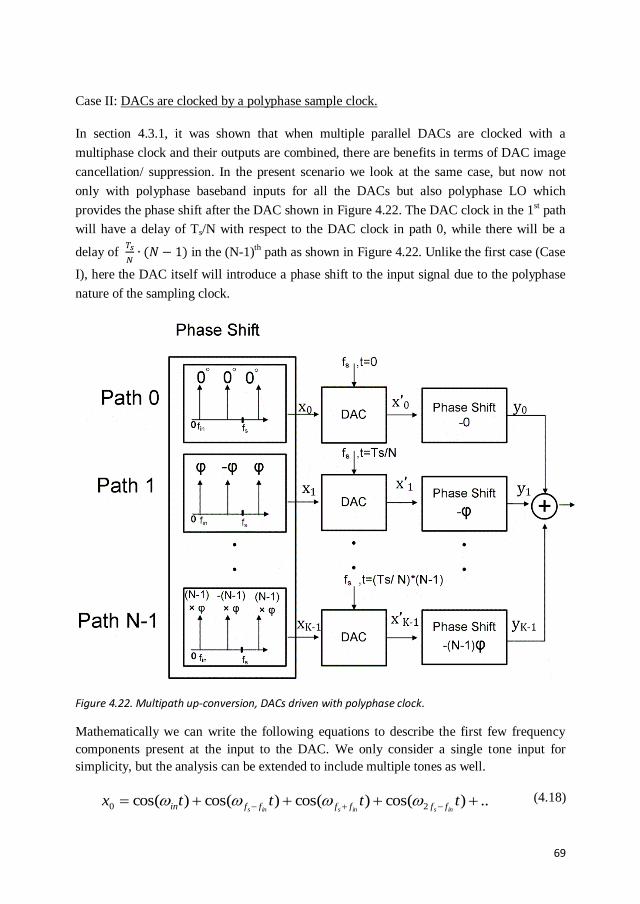
69
Case II: DACs are clocked by a polyphase sample clock.
In section 4.3.1, it was shown that when multiple parallel DACs are clocked with a
multiphase clock and their outputs are combined, there are benefits in terms of DAC image
cancellation/ suppression. In the present scenario we look at the same case, but now not
only with polyphase baseband inputs for all the DACs but also polyphase LO which
provides the phase shift after the DAC shown in Figure 4.22. The DAC clock in the 1st path
will have a delay of Ts/N with respect to the DAC clock in path 0, while there will be a
delay of
in the (N-1)th path as shown in Figure 4.22. Unlike the first case (Case
I), here the DAC itself will introduce a phase shift to the input signal due to the polyphase
nature of the sampling clock.
Figure 4.22. Multipath up-conversion, DACs driven with polyphase clock.
Mathematically we can write the following equations to describe the first few frequency
components present at the input to the DAC. We only consider a single tone input for
simplicity, but the analysis can be extended to include multiple tones as well.
..)cos()cos()cos()cos( 20 ttttxinsinsins ffffffin (4.18)

70
....)360
cos()360
cos(
)360
cos()360
cos(
2
1
Nt
Nt
Nt
Ntx
insins
ins
ffff
ffin
(4.19)
...))1(360
cos())1(360
cos(
))1(360
cos())1(360
cos(
2
1
KN
tKN
t
KN
tKN
tx
insins
ins
ffff
ffinK
(4.20)
The following equations describe the output of the DAC, neglecting the sinc response at the
moment, and only considering the phase variation due to the polyphase DAC clock.
..)cos()cos()cos()cos(' 20 ttttx
insinsins ffffffin (4.21)
We take OS= fs/ fin
....))12()360
(360
cos(
))1()360
(360
cos(
))1()360
(360
cos(
))360
(360
cos('
2
1
OSOSNN
t
OSOSNN
t
OSOSNN
t
OSNNtx
ins
ins
ins
ff
ff
ff
in
(4.22)
Comparing the above equation with 4.22, we see that for the fundamental input signal,
aside from the nominal phase shift of 360°/N required by the polyphase multipath
technique, there is an additional phase shift of OSN
360 caused due to the delay of the
multiphase DAC sampling. The first DAC image occurring at fs-fin, will undergo a phase
shift of OSN
360× (OS-1), as it occurs at (OS-1) times the input signal.

71
The above equation can be extended to the (K-1)th path as follows.
...))12())1(360
()1(360
cos(
))1())1(360
()1(360
cos(
))1())1(360
()1(360
cos(
)))1(360
()1(360
cos('
2
1
OSKOSN
KN
t
OSKOSN
KN
t
OSKOSN
KN
t
KOSN
KN
tx
ins
ins
ins
ff
ff
ff
inK
(4.23)
After upconversion by a single tone at frequency ωLO, the following equation results
)..cos()cos()cos(
)cos()cos(
)cos()cos()cos(
22
0
tttttt
tttt
tttttty
insinsins
insins
ins
ffLOffLOffLO
ffLOffLO
ffLOinLOinLO
(4.24)
....))12()360
(cos(
))12()360
(720
cos(
))1()360
(720
cos(
))1()360
(cos(
))1()360
(cos(
))1()360
(720
cos(
)360
(720
cos(
)360
(cos(
2
2
1
OSOSN
tt
OSOSNN
tt
OSOSNN
tt
OSOSN
tt
OSOSN
tt
OSOSNN
tt
OSNNtt
OSNtty
ins
ins
ins
ins
ins
ins
ffLO
ffLO
ffLO
ffLO
ffLO
ffLO
inLO
inLO
(4.25)

72
))...12())1(360
(cos(
))12())1(360
(
)1(720
cos(
))1())1(360
(
))1(720
cos(
))1())1(360
(cos(
))1())1(360
(cos(
))1())1(360
(
))1(720
cos(
)))1(360
())1(720
cos(
)1()360
(cos(
2
2
1
OSKOSN
tt
OSKOSN
KN
tt
OSKOSN
KN
tt
OSKOSN
tt
OSKOSN
tt
OSKOSN
KN
tt
KOSN
KN
tt
KOSN
tty
ins
ins
ins
ins
ins
ins
ffLO
ffLO
ffLO
ffLO
ffLO
ffLO
inLO
inLOK
(4.26)
If we assume 2·OS >> 1, so that (2·OS-1) ~ 2·OS

73
)))...1(720
(cos(
)cos(
))1())1(360
(
))1(720
cos(
))1())1(360
(cos(
))1())1(360
(cos(
))1())1(360
(
))1(720
cos(
)))1(360
())1(720
cos(
)1()360
(cos(
2
2
1
KN
tt
tt
OSKOSN
KN
tt
OSKOSN
tt
OSKOSN
tt
OSKOSN
KN
tt
KOSN
KN
tt
KOSN
tty
ins
ins
ins
ins
ins
ins
ffLO
ffLO
ffLO
ffLO
ffLO
ffLO
inLO
inLOK
(4.27)
So we see that the frequency components at ins ffLO 2 will have the same phase in
each path and will not cancel in a polyphase multipath system but rather add up. This
frequency component is also free of N, therefore the number of paths will not effect this
term and it will remain uncancelled.
The desired signal at inLO will not align exactly in phase and all the other frequency
components in (4.27) will not align exactly in anti phase and there would be some residual
frequency components remaining. This is shown in the 4-path example in the next
paragraph.
To understand better why cancellation is not achieved, the 4-path example shown in Figure
4.23 can be visualized. Here again it is assumed that the baseband frequency is at 10MHz
and fs is at 200MHz while the LO is at 10GHz.

74
Figure 4.23.Multiphase upconversion where the DACs are also driven with polyphase clock.
Figure 4.24. Phasor diagram for the frequency components at the summation point of Figure 4.23.
The DAC blocks also indicate the phase delay they cause at different frequencies (i.e. fin, fs-
fin, fs+fin) for a 20 times higher clock frequency than the input signal. One sample phase
delay is equivalent to Ts=360°/20 =18°. This implies that Ts/4= 4.5° (see eq.(4.23)). The
fundamental signal in the first path will undergo a phase shift of 4.5° after passing through
the DAC, while the signal at fs-fin which is at 19 times higher in frequency will undergo a
phase shift of 19 ×4.5° = 85.5°. The phase change after each block is also shown. Just
before summation it is seen that the fundamental components and also the images do not
align exactly in anti phase as shown in Figure 4.24. Therefore there will be some residual
frequency components (due to incomplete cancellation) in the frequency spectrum as
predicted by (4.27).

75
Figure 4.25 shows the simulated output spectrum of the system in Figure 4.23, where the
upconverted images around ωLO+ωfs are suppressed but not completely cancelled. Another
disadvantage here is that the image of the fundamental at ωLO-ωfin is not completely
cancelled due to the non-anti phase alignment of this image, due to the additional phase
shift caused by the polyphase DAC sample clock. This drawback can be overcome by delay
compensating the input signal such that it aligns in such a way that the image signal at ωLO-
ωfin cancels out. This delay compensation is illustrated in the Figure 4.26 for a single tone,
but can be extended for multiple tones as well.
Figure 4.25.Output Spectrum of 4-path upconversion with DACs driven with multiphase sample clock.
As compared to Figure 4.23, the input signal is now also adjusted to compensate for the
phase shift caused by the polyphase sample clock of the DACs. It can be seen that the
fundamental component in the 2nd, 3rd and 4th paths are compensated by 4.5°, 9° and 13.5°
respectively. These values can be calculated by putting K=2, 3 and 4, OS=20 and N=4 in
(4.26). Just before the summation, the fundamental components are now aligned in phase,
which also enables the image at ωLO-ωfin to be cancelled.
The output spectrum for a 4-path upconverter is shown in Figure 4.27, while an 8-path
upconversion spectrum is shown in Figure 4.28. The upconverted DAC image at ωLO+2ωfs-
ωfin remains uncancelled in both cases due to its in-phase addition after summation as
predicted by (4.27). Simulation for different number of paths shows that this image remains
uncancelled. A two-tone simulation (5MHz and 20 MHz) for an 8-path upconversion is also
shown in Figure 4.29, to confirm that the delay compensation technique also works for
multi-tones.

76
Figure 4.26 Multiphase upconversion where the DACs are driven with multiphase clock and the inputs are delay compensated.
Figure 4.27.Output Spectrum of 4-path upconversion with DACs driven with multiphase sample clock and inputs delay compensated resulting in cancellation of the term at ωLO-ωfin.

77
.
Figure 4.28. Output Spectrum of 8-path upconversion with DACs driven with multiphase sample clock and inputs are delay compensated.
Figure 4.29. Output Spectrum of two tones (5 MHz and 20 MHz) 8-path upconversion with DACs driven with multiphase sample clock and the two-tone inputs are delay compensated.
The conclusion we draw from the above discussion is that polyphase multipath
upconversion using polyphase DAC clocks is more beneficial for cancelling DAC images
compared to the case where the same clock is used for all parallel DACs. The image

78
occurring at ωLO+2ωfs-ωfin , which is the closest most dominant image remains uncancelled
due to its in-phase addition at the output, while the image of the fundamental around the LO
can be cancelled if proper phase compensation is provided to the inputs.
4.4 DAC Implementation In this section we discuss some implementation options of an on-chip DAC to drive the
multipath mixers. Since the first set of phase shifters are in digital, the digital data for each
path needs to be converted to the analog domain to drive the mixers constituting the Power
Upconverter (PU). Two different possibilities to implement these DACs are discussed in
the following sub sections.
4.4.1 N parallel DACs
One possibility is to use separate DACs running at the sample frequency of the digital data
for each phase shifted data stream shown in Figure 4.30. BB0, BB1,… are the analog
baseband signals driving the multipath mixers. The architecture of Figure 4.30 could be
implemented on chip, but it would make the design quite large and complex. Also
maintaining good matching between the DACs would be a challenge, since each DAC
would have its own reference voltage or current. Another possibility is to use one reference
voltage ladder but realize separate switching networks for each set of phase shifted digital
data as shown in Figure 4.31. As the voltage reference is common for all the digital-to-
analog switching networks, any variation in the reference voltage would be common to all
the paths. Also the distortion in each path due to reference variation would be minimized at
the output as compared to the architecture in Figure 4.30, although a disadvantage would be
some crosstalk due to switching noise coupling into the ladder.
The coding scheme for the switching networks could be either binary or one-hot encoded.
Figure 4.32 shows a 2-bit architecture of these two different encoding schemes. In
simulation we saw that an 8-bit binary coded scheme was able to achieve similar inter-
modulation distortion performance (for the same sample frequency and load) if the DAC
switch size was made ten times bigger than the one used for the one-hot encoded switches
(switch size chosen close to minimum size). This difference was mainly due to the higher
number of switches in series in the path of the binary encoded architecture from the ladder
to the load. As the switching networks have to be parallel eight times, so the total area
would also have to be considered. Therefore just considering the switching network size,
the one-hot coded scheme would be preferable.

79
Figure 4.30 Separate Reference generation and switching network for each DAC.
Figure 4.31 One reference ladder and separate switching networks generate the multiphase baseband, to have similar distortion in all paths as compared to Figure 4.30.

80
Figure 4.32. Binary (left) versus one-hot encoding (right)
4.4.2 One DAC with de-interleaving
Another possibility to generate the eight analog multiphase signals is to use one stand alone
DAC running at 8x the sample rate as shown in Figure 4.33. It generates a time interleaved
(multiplexed) version of all the 8 baseband paths, which are separated again by de-
interleaving switches and hold functions to generate the eight analog signals (BBO,
BB1..BB7). The eight phase Polyphase clock required to drive the de-interleaving switches,
can be generated by the circuit discussed in section 5.2.1. It should be noted that the 8x
frequency required as input to such a polyphase clock generator circuit would be the same
as the 8x sample frequency for the DAC, so an additional reference clock would not be
required. In order to have increased chip testing flexibility, we can generate the digital
multiphase baseband signals and use a digital to analog convertor off chip for evaluation
purposes. In such a scenario only one analog input pin would be required for the chip to
convey the high speed DAC output to the de-interleaving switches, which are implemented
on chip. The off-chip DAC and the de-interleaving interface should preferably be
impedance matched to a transmission line to minimize reflections.
The 8-phase polyphase clocks driving the de-interleaving switches can have 1/8 duty cycle
as shown in Figure 4.34. This ensures that only one de-interleaving switch is tracking the
input signal while the other paths are holding their last sample value. This way one path
does not influence the other significantly. An implementation of the de-interleaving
switches is presented in the next chapter.

81
Figure 4.33 One DAC and de-interleaving
Figure 4.34. 8-phase clock driving the de-interleaving switches
4.5 Digital Interpolation Filter
The output of a digital to analog conversion contains many images of the input signal
occurring around the sampling clock as discussed in section 4.3. These images are
conventionally suppressed via an analog reconstruction filter. A digital interpolation filter
allows for going to a higher sample rate (oversampling) which shifts the images to a higher

82
frequency. The oversampling in combination with an analog filter relaxes the
reconstruction filtering requirements. The digital filter becomes more crucial if the input to
the chip has a low oversampling rate (or nyquist rate) restriction, e.g. due to DAC-bus or
DAC speed limitations. If the chip interface can sustain a high sample rate and further
relaxation in analog reconstruction filtering is not required, then on-chip oversampling may
not be needed. For a cognitive radio transmitter an analog signal bandwidth of at least
6MHz is desired, which would imply 3MHz in both the I and Q channels. Oversampling the
digital baseband using digital interpolation depends upon how much area and power can be
sacrificed in the digital domain to gain the benefit of analog filter relaxation. Another
criterion to consider while designing such a digital filter is the speed limits of the IC
technology being used for implementation. Considering these factors and aiming for better
than 50dB suppression of the DAC images, an 8 times oversampled baseband (fs=48 MHz)
in combination with a 2nd order analog filter can be chosen. The 8 times oversampling in
combination with the zero order hold response of the DAC provides 30 dB suppression
(from (4.8)) of the second DAC image (occurring around 2*fs) which remains un-cancelled
when upconverted as shown in Figure 4.28.
The remaining suppression can be provided by a 2nd or higher order analog filter. This can
be seen in Figure 4.35, where the sinc response (from the sinc response equation 4.8) is
plotted as a function of the frequency. Also an ideal low pass 1st order RC filter response,
and a 2nd order (cascade of two RC filters) filter response is also shown. The 2nd order filter
has a -3dB corner of 10MHz. Adding up the suppression of the sinc and the 2nd order filter
<-40 dBc is achieved around fs (48MHz) and <-55dBc around 2fs (96MHz).
4.5.1 Digital Filter Design
The digital interpolation filter should be linear phase so that it can provide a frequency
independent delay. This would mean that it provides the same phase shift at one particular
frequency in each path, so it does not impact the relative phase relationship in each path. A
linear phase interpolation filter can be implemented by a direct-form FIR filter [13]. A
simple 11 tap filter [13] architecture of a 2 times interpolation stage can be implemented as
shown in Figure 4.36. Here the coefficients were determined by using the filter design
utility fdatool in MATLAB. Here the taps 1, 3, 7 and 9 are zero (not present in Figure 4.36).
Since the other coefficients are symmetric around the centre tap, the architecture can be
further simplified by reducing the number of multiplications. The filter achieves better than
50dB suppression above the stop-band as shown in Figure 4.37. Three such stages are
cascaded in series to achieve 8 times oversampling in total. Although such a filter design
can also be optimized further by having more taps in the earlier stages which work at lower
frequency and hence would consume low power. Performance of an interpolation stage to

83
relax analog filtering can be improved further with newer CMOS technologies. An 8x
interpolation filter designed with the architecture shown in Figure 4.36 and synthesized in
Cadence synthesis tool in a 160nm CMOS process consumed an area of 190µm × 190µm
(VHDL code in APPENDIX C). The filter worked with an output frequency of 50MHz,
with a 16-bit processing resolution and the expected power consumption is 10mW. The
power consumption of this non-optimized design is still relatively low compared to the
overall power consumption of the complete transmitter (discussed in the next chapter).
Figure 4.35. Suppression due to sinc response and an RC first order and an RC second order low pass Filter. Adding the attenuations of the sinc response and second order filter close to 96MHz, achieves < -55dB.

84
Figure 4.36 Structure for a 2x interpolation filter
Figure 4.37 Interpolation filter response normalized to clock frequency
85
4.6 Conclusion
An important issue in the design of a complete digital to RF polyphase multipath
transmitter is the mixed signal system design. In this chapter requirements on the mixed
signal system design are discussed and possible solutions are analyzed. It is shown that it is
possible to generate the multiphase baseband signals required for an 8-path upconversion
by using simple vector addition, employing a simplified vector modulator type of
architecture. A design was synthesized in Cadence synthesis tool in 160nm CMOS running
at 50MHz and 16 bit resolution. The estimated power consumption is only 2.5mW.
The multipath polyphase transmitter design can in principle cancel harmonics responses in
the DAC output resulting from quantization errors. However, since inter-modulation terms
remain un-cancelled so its usefulness is limited. For a single-tone and multi-tone transmit
signal, at least 8dB and 10dB per bit SFDR can be achieved assuming the first set of phase
shifters are ideal while the second set of phase shifts are provided by mixer, whose
nonlinearity is modeled as a power series. Hence, in order to keep the SFDR due to limited
DAC resolution better than 50dB at least a 7 bit DAC resolution is required.
It is possible to cancel the first dominant DAC image by using a multiphase DAC
architecture. The dominant non-cancelled image is then at 2*fs, which occurs due to its
almost in-phase addition in all the paths.
We can implement either a single DAC on chip, using a single voltage reference and
multiple switching networks, or we could implement a single DAC and use on chip de-
interleaving switches to make the 8 analog baseband signals. For testing flexibility one
external DAC and on chip de interleaving was chosen.
Digital interpolation filters can relax the reconstruction filtering requirement to a second
order filter with limited power overhead. A digital FIR filter design was synthesized in
Cadence synthesis tool in 160nm CMOS running at 50MHz and 16 bit resolution. The
estimated power consumption is only 10mW.
References
[1] S. K. Garakoui, E. A. M. Klumperink, B. Nauta, and F. E. van Vliet, "Time delay circuits: A quality criterion for delay variations versus frequency," in Circuits and Systems (ISCAS), Proceedings of 2010 IEEE International Symposium on, 2010, pp. 4281-4284.
86
[2] F. Behbahani, Y. Kishigami, J. Leete, and A. A. Abidi, "CMOS mixers and polyphase filters for large image rejection," Solid-State Circuits, IEEE Journal of, vol. 36, pp. 873-887, 2001.
[3] B. Razavi, RF Microelectronics. Upper Saddle River, NJ: Prentice Hall, 1998. [4] Y. Yu, P. G. M. Baltus, and A. H. M. van Roermund, Integrated 60GHz RF
Beamforming in CMOS: Springer, 2011. [5] N. Blachman, "The intermodulation and distortion due to quantization of
sinusoids," Acoustics, Speech and Signal Processing, IEEE Transactions on, vol. 33, pp. 1417-1426, Dec. 1985.
[6] M. J. M. Pelgrom, Analog-to-Digital Converters: Springer, 2010. [7] M. S. Oude Alink, A. B. J. Kokkeler, E. A. M. Klumperink, K. C. Rovers, G. J.
M. Smit, and B. Nauta, "Spurious-Free Dynamic Range of a Uniform Quantizer," Circuits and Systems II: Express Briefs, IEEE Transactions on, vol. 56, pp. 434 - 438, June 2009.
[8] R. Shrestha, E. A. M. Klumperink, E. Mensink, G. J. M. Wienk, and B. Nauta, "A Polyphase Multipath Technique for Software-Defined Radio Transmitters," Solid-State Circuits, IEEE Journal of, vol. 41, pp. 2681-2692, 2006.
[9] R. Gray, "Quantization noise spectra," Information Theory, IEEE Transactions on, vol. 26, pp. 1220-1244, Nov. 1990.
[10] P. T. M. van Zeijl and M. Collados, "On the Attenuation of DAC Aliases Through Multiphase Clocking," Circuits and Systems II: Express Briefs, IEEE Transactions on, vol. 56, pp. 190-194, March 2009.
[11] J. Deveugele, P. Palmers, and M. Steyaert, "Parallel-Path Digital-to-Analog Converters for Nyquist Signal Generation," Solid-State Circuits, IEEE Journal of, vol. 39, pp. 1073-1082, 2004.
[12] R. G. Lyons, Understanding Digital Signal Processing Upper Saddle River, NJ.: Prentice Hall, 2001.
[13] X. He, J. van Sinderen, and R. Rutten, "A 45nm WCDMA Transmitter Using Direct Quadrature Voltage Modulator with High Oversampling Digital Front-End," in International Solid State Circuits Conference, 2010.

87
CHAPTER FIVE
5 Polyphase Multipath Transmitter Implementation (This chapter is taken from the sections III-VI of the paper published in the IEEE Journal of
Solid State Circuits [1]. The only differences are the addition of section 5.2 and the Figures
5.5, 5.6, 5.7, 5.16 and 5.24).
This chapter describes the implementation in 160nm CMOS of the 8-path polyphase
multipath transmitter. For flexibility reasons an off chip DAC was utilized. Each of the 8-
paths in Figure 5.1 consist of a sample and hold block (discussed previously in section
4.4.2), buffer and baseband filter (mentioned previously in section 4.5) and a switched
transconductor upconversion mixer. The current output of the mixer blocks is combined to
drive the antenna load. A tunable low-pass filter at the output (discussed previously in
section 3.2.1) provides filtering over a wide band. A replica bias circuit is used to stabilize
the bias current of the mixers over Process-Voltage-Temperature (PVT) variations,
attempting to keep the output power stable. An 8-phase LO with 1/8 duty-cycle drives the
eight sample and hold (S&H) switches (discussed previously in section 4.4.2). Another 8-
phase LO with ~7/16 duty-cycle (discussed previously in section 3.4) drives the eight up
conversion mixer switches.
Figure 5.1 Block Diagram of the implemented 8-path Transmitter.

88
The circuit implementation did not aim for any specific standard but rather explored what
can be achieved with this technique in practice, especially compared to [2]. Circuit details
for these blocks are given in the following sections.
5.1 Baseband Generation
Figure 5.2 shows the circuit present in each baseband and upconversion path, driven by an
(external) DAC. The use of one DAC for all 8-paths is preferable to maximize matching of
the signal paths. The 8 polyphase baseband signals are generated digitally and drive the
DAC in a time interleaved way at 8 times the baseband sampling frequency. The sample
switch S1 in the sample and hold (S&H) of each path de-interleaves the DAC signal into 8
parallel analog baseband signals. To this end, the S&H switches are driven by an 8-phase
non-overlapping 1/8 duty-cycle clock (S&HLO).
Figure 5.2 One Baseband to RF path with S&H, filter and mixer.
The S&H is designed such that it is not limiting the linearity of the upconverter at full
swing; also the switch size is small which does not require significant power consumption.
The interleaving mechanism can be understood as the generation of a high frequency
signal, while the de-interleaving could be understood as the down-conversion of a high
frequency signal to baseband along with the generation of the required phases. Figure 5.3
shows an ideal time domain output of the DAC for a single tone polyphase baseband. Two
of the de-interleaved baseband signals are also shown for visualization. The buffer provides
isolation between the S&Hs and the baseband filters. Isolation during the on-time of the
S&H is further improved by the switch , which disconnects the baseband RC filter from
the S&H during the S&H switching transients [3]. For a channel bandwidth of 6MHz
(3MHz in both I and Q), the sampling frequency (fs) was set at 48 MHz.

89
Figure 5.3 DAC output containing all the 8 polyphase baseband signals (2 of the phases are in bold).
Figure 5.4 Sinc and RC low-pass filtering, achieving <-55dBc at 2×fs.
The sinc response due to the DAC hold function and the baseband filter response are shown
in Figure 5.4. The multiphase baseband when upconverted via the multiphase mixers results
in cancellation of the first DAC replica image (see section 4.3.2 (case 2) and [4]) occurring
around fs. The second DAC replica image around 2fs=96MHz is suppressed to <-55dBc due
to the combination of RC filter and the sinc response as shown in Figure 5.4 (adding the
attenuations). A cascade of three RC sections with increasing resistance but with equal pole
frequency of 10MHz was used as low-pass filter. A replica bias circuit (discussed in section
5.4) controls the bias current of the mixer by adjusting Vbb.

90
5.2 8-phase LO generation
Theoretically, a 7/16 duty-cycle [5] mixing clock can be realized by dividing a 16x higher
clock. Compared to a DLL, this is more power efficient for the same mismatch accuracy
[6], but there is a limit to the maximum frequency which can be achieved. In the 160nm
CMOS technology that we used, 16x800MHz was problematic.
Since 0.4365 is rather close to 0.50, we use an 8-phase 50% duty-cycle clock generated by
a divide-by-4 circuit and delay the rising edge (only by a ratio of 0.063) to reduce duty-
cycle. The buffer afterwards again makes the edge steep. The 8-phase 50% duty cycle clock
is generated by a divide by four circuit, where both outputs of the flip flop are used to get
all the 8 phases shown in Figure 5.5. The flip flops are made using Transmission gate (TG)
logic, which provides better power and mismatch performance as compared to some other
logic families [7, 8]. A high frequency sine wave is converted to a differential signal via an
external balun. It is converted into a square wave via the on chip self biased inverter buffers
shown in Figure 5.6. Two on chip 50 Ω resistors provide the matching.
In circuit simulation, the divide by 4 circuit was able to function properly upto an LO
frequency of 1.2GHz equivalent to 4.8GHz input frequency for the slowest corner of the
160nm CMOS process model library.
Figure 5.5 Divide by 4 implemented as a chain of flip flops
D
D
Q
Q
D
D
Q
Q
D
D
Q
Q
D
D
Q
Q
CLK CLK
D
D
Q
Q
CLK
CLK
CLK
LO1
LO2
LO3
LO4LO5
LO6
LO7
LO8

91
Figure 5.6 Sine wave input converted to a differential square wave on chip.
5.2.1 Generating 1/8 duty cycle for sample & hold switch
The divide by 4 circuit is used not only for the LO path but a copy of the same circuit is
utilized to generate the multiphase clock for the baseband sample and hold circuit. Since the
DAC is switching at 8 times the sampling frequency, a divide-by-eight circuit is required
which divides the DA clock to the sample rate needed by the sample and hold switches.
Therefore a divide by two circuit was added before the divide by four as shown in Figure
5.7. To make the 1/8 duty cycle, AND gates are used which combine two of the phases also
shown in Figure 5.7. To avoid overlap between the clocks, the rise and fall times were
adjusted at the output inverter stage inside the AND gate. This was done by making the
NMOS of the inverter stronger than the PMOS, so that the fall time is faster than the rise
time, allowing the crossover point of the adjacent clock phases to be low.
Figure 5.7. Logic to convert 50% duty cycle to 1/8 duty cycle

92
5.3 Duty-Cycle Control Circuit Design
Figure 5.8 shows how the controllable duty-cycle is realized on circuit level, by delaying
the rising edge of a 50% clock. The clock divider output is buffered and then an inverter
with controllable rising edge delay drives the last buffer stage. The control is accomplished
via a tunable resistor, implemented as a triode PMOS transistor (MP2). For control
purposes, monotonic control is desired, which is realized by controlling the gate voltage of
the triode transistors by an intrinsically monotonic resistor ladder DAC. In order to achieve
this control over multi-octaves of frequency range, additional triode transistors can be
added via switches S1-S5 as shown in Figure 5.9, where DAC voltage (VDAC) is shared.
There are two main requirements on the design: 1) there should be sufficient resolution to
keep the duty-cycling variations within 0.1% as discussed in section 3.2. 2) The required
duty-cycle should be provided over multiple octaves of frequency range. The following
sub-sections describe how these requirements can be met.
Figure 5.8. Duty-cycle control varying RT, implemented as a triode PMOS MP2 driven by a ladder
DAC.
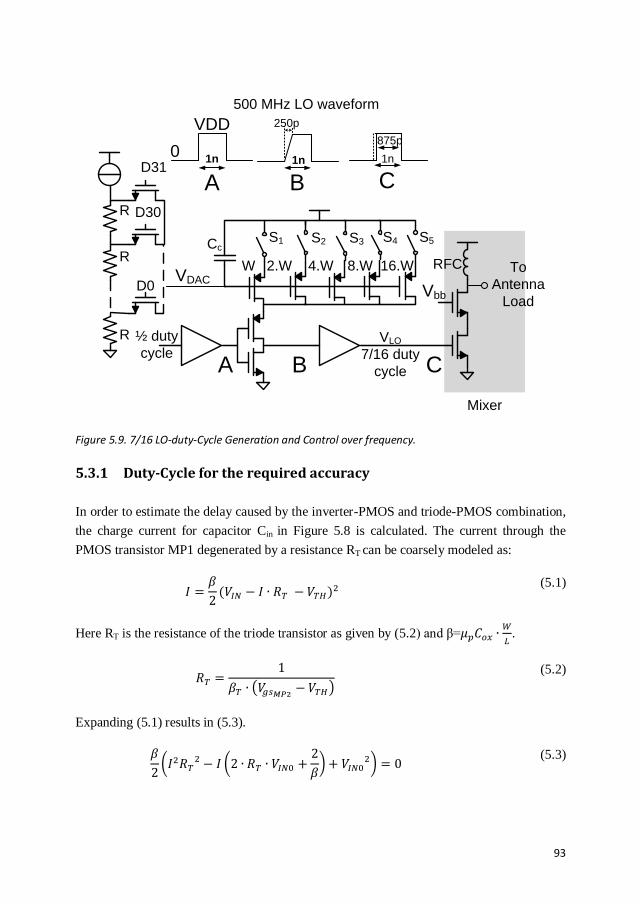
93
Figure 5.9. 7/16 LO-duty-Cycle Generation and Control over frequency.
5.3.1 Duty-Cycle for the required accuracy
In order to estimate the delay caused by the inverter-PMOS and triode-PMOS combination,
the charge current for capacitor Cin in Figure 5.8 is calculated. The current through the
PMOS transistor MP1 degenerated by a resistance RT can be coarsely modeled as:
(5.1)
Here RT is the resistance of the triode transistor as given by (5.2) and β=
.
(5.2)
Expanding (5.1) results in (5.3).
(5.3)
Mixer
S1 S2 S4
W 2.W 8.W
½ duty
cycleVLO
7/16 duty
cycle
S3
4.W
CcS5
16.W
Vbb
A B C
VDACD0
D31
D30
R
R
R
250p
1n 1n 1n
875p
A B C
0
VDD
500 MHz LO waveform
To
Antenna
Load
RFC

94
Figure 5.10 Calculated and Simulated Delay.
Where VIN0= VIN- VTH, Solving the quadratic equation of (5.3) results in (5.4).
(5.4)
This current can be used to estimate the delay due to the triode PMOS by the following
equation.
td= Cin ΔV / I (5.5)
where td is the rise time delay, Cin is the capacitance at the input of the last buffer and ΔV is
taken as VDD/2, the point where the last buffer switches. Equation (5.5) is plotted in Figure
5.10, after substituting the values of Cin=300fF, β=12.5mA/V2, VIN = 1.5, VTH = 0.5 and βT
is 0.78mA/V2 for the LSB triode PMOS (MP2). Figure 5.10 also shows the simulated (in
160nm CMOS process) values of the delay plotted as a function of Vgs of the triode (MP2)
transistor. The delays for the 2, 4, 8 and 16 times the LSB triode PMOS size are also
shown. As |Vgs| for MP2 decreases from 1.5V to 1V, the delay becomes more than half of
its initial value. A higher delay can be achieved by reducing the |Vgs| further, but larger
|Vgs| is better to keep the variation in the resistance of MP2 limited due to Vth mismatch.
Also larger |Vgs| keeps the MP2 PMOS in deep triode. The steepness of the delay curve is
lower at larger |Vgs|, which is desired since it provides smaller delay steps. Therefore the

95
range of Vgs chosen is from -1.5V to -1V. The gate voltage required is generated by a 5-bit
resistor ladder DAC which achieves a resolution of 1.25ps (for 800MHz LO) with some
margin (from (5.5)). High frequency VDD variations are coupled to the gate of the triode
transistors with the capacitor Cc, attempting to leave Vgs unaffected.
5.3.2 Duty-Cycle over a Frequency Range
In order to achieve the required duty-cycle over the 3 octaves frequency range an estimate
is needed of the resistance value of the tunable resistor. This resistance value should satisfy
the boundary conditions of achieving the required delay over the frequency range. The total
rising edge delay required is about 1/8 of the LO time period. As there will always be some
fall time present in the LO path, that has to be taken into consideration as well. Also,
depending on the exact shape of the transition edges, some fine tuning may be needed.
From simulations done on the LO path, the falling edge delay time at the mixer switch
remains around 70-90ps for the 100-800- MHz frequency range. After subtracting the fall
time from the required rising edge delay time, an estimate of the rising edge delay td is
found. This delay is in the range of 60ps to 1.1ns (for the highest and lowest frequency).
The resistor values can be estimated by substituting (5.4) in (5.5) and solving the quadratic
equation for RT.
(5.6)
Solving (5.6) we find that the biggest resistor required is almost 13 times bigger than the
smallest value. A 5-bit resolution of the parallel triode transistor was chosen to be able to
cover the frequency range with some overlap between switching of the binary weighted
PMOS transistors. The switch sizes S1..S5 in Figure 5.9 were made big enough so as to not
be dominanting the control mechanism. Since the DAC voltage is distributed to all the
paths with some series resistance, a local decoupling capacitor is used to bypass the high
frequency voltage components that can couple from the LO path to the DAC output.
5.3.3 Duty-Cycle variation with Temperature
In order to assess the behavior of the duty cycle control circuit with temperature variation,
circuit simulations were performed on the circuit Figure 5.9 and the duty cycle was
measured at the input of the mixer switch (node C). The temperature was swept from -30°C
to 80°C, while the optimum code was set for 20°C. The results in Figure 5.11 show that for
around 25°C increase in temperature the duty cycle varies by 0.1%. Further simulations

96
including the mixer reveal that there is a variation in harmonic responses of about 1dB from
the optimum code if the temperature varies by ±10°C (20°C in total). So we would
recommend doing an offline re-calibration for each 20 degree variation in temperature, as
real time calibration during operation might cause harmful interference. Frequent
recalibrations are probably not needed once chip temperature is stable within about 20
degrees.
Figure 5.11. Duty Cycle Variation with Temperature.
5.4 Replica Biasing A replica biasing circuit was utilized as shown in Figure 5.12. The aim was to keep the
mixer current and hence delivered power to the load controlled by a bias current. To this
end a scaled replica of the switched gm mixer is biased by current Ibias. A diode-connected
scaled gm transistor absorbs the current and generates a voltage Vref. The gate of the lower
transistor in the mixer replica is connected to VDD to mimic the ON state of the mixer
switch. Now Vref is the wanted DC bias voltage corresponding to wanted mixer bias point.
This voltage should be generated by all buffers if their input is equal to VDAC_DC, the middle
of DAC range (externally generated here by a voltage source as the DAC was external). To
do this, a buffer replica is connected to VDAC_DC and an error amplifier adapts the gate of
the PMOS current source MPcur. The amplifier is implemented by a two stage op-amp. Its
high gain forces voltage Vtrack equal to Vref by adjusting voltage Vfilter_bias, making the mixer
bias insensitive for PVT variations. The Vfilter_bias voltage is used as bias for all the baseband
paths. The compensation capacitor Cc makes sure that the phase margin of the loop is more
than 70 degrees over all process corners.

97
Figure 5.12 Replica Biasing Circuit adjusting Vfilter_bias.
5.5 Mixers The switched transconductor (switched-gm) mixer architecture in which a transconductor is
switched on and off [9] was utilized to provide frequency translation as well as power gain.
Figure 5.13a shows the switched-gm mixer used in [2], where the lower transistors
implement the switches and the upper ones the transconductor. In the current design, a
split-switch architecture for the switched-gm mixer was utilized as shown in Figure 5.13b,
where Vo+ and Vo- are the differential outputs across the load (2×50Ω).
The switch size was divided equally between the two arms of the gm, with negligible effect
on the LO-buffer loading. This was done to shift the compression point to a higher input
swing and to improve linearity. The ON resistance of the mixer switch now acts as source
degeneration for the transconductor. As discussed in [2, 10] the optimum size of gm
transistors and switch transistors is equal for maximum amplification for a given area.
However, reducing the size of the switch is beneficial for reducing the power consumption
in the driver buffers.
For the current design a size of 100µm/0.16µm was chosen for each switch transistor and
200µm/0.16µm for each trans-conductor. Simulations show that using the split-switch
mixer (Figure 5.13b) improves the compression point and OIP3 by 3dB and 1dB
respectively as compared to the shared-switch mixer (Figure 5.13a).

98
Figure 5.13 (a) Mixer used in [2] (b) Mixer in current design
5.6 Tunable 1st Order Low-Pass Filter A tunable RC low-pass filter is applied at the output of the mixer to suppress the higher
harmonics. A bank of switchable binary weighted capacitors in combination with the load
resistor (50Ω, single ended) (shown in Figure 5.14) provide a first order RC roll off, where
the current source represents the switched-gm mixers.
Figure 5.14 Switch Capacitor bank providing output filter tuning.
The NMOS switch sizes were kept large enough to keep their ON resistance low, so as not
to limit the suppression achieved. The magnitude of the fundamental component can vary
significantly with LO frequency if there is not enough resolution in the capacitance bank. In
order to keep these variations <0.5 dB from the nominal value, a 5 bit resolution was
chosen. Alternatively a coil can be added to realize a band-pass filter with tunable center
frequency. This can give more suppression but results in less tuning range for the same

99
capacitor variation. Since this filtering occurs after the mixers, any nonlinearity added by
this filter would not be cancelled. Therefore fringe capacitors were utilized, which are more
linear than MOS capacitors.
Figure 5.15 Chip micrograph with active area < 0.32mm2 in 160nm CMOS
Figure 5.16. Chip Measurement Setup

100
5.7 Measurement Results
The transmitter was implemented in a 160nm CMOS process, and its die photo and
measurement setup is shown in Figure 5.15 and Figure 5.16 respectively. The RF choke
(see Figure 5.2) and the load (2×50Ω) are off chip. Figure 5.17 shows the measured
fundamental power at 400MHz LO, as well as the 7th and 9th harmonic response for all the
1024 (5+5 bits) duty-cycle codes. Here the code 0 implies a duty-cycle ratio close to 0.5
(S1-S5 in Figure 5.9 all ON) and higher codes gradually move towards lower duty-cycle
ratios as explained below. The abrupt jumps in the harmonic response occur when a binary
scaled PMOS transistor is turned ON/OFF by S1-S5. The smaller steps occur when
selecting a next tap of the ladder DAC, which increases the VDAC increasing RT and hence
decreasing the duty-cycle. Clearly, there are more than enough codes to fine tune the
harmonic power with better than 1 dB precision via the ladder DAC (see inset of Figure
5.17).
This works uptill the maximum LO frequency of 800MHz, beyond which the divider stops
working. At code 512, the MSB switches OFF and due to the un-symmetric layout of the
MSB PMOS, there is an upward jump in the harmonic response, which causes some
repetition in the harmonic responses upto around code 700. This repetition along with the
overlap in codes (2 or more codes giving the same harmonic response), can easily be
detected and removed by a one-time calibration.
Figure 5.17. Magnitude of 7th and 9th harmonics vs.Duty-Cycle code(LO at 400MHz). Bigger markers
are for those duty cycle codes which give non-overlapping harmonic response.

101
Figure 5.18. Magnitude of harmonics vs. Non-Overlapping Duty-Cycle code(LO at 400MHz). Same
graph as Figure 5.17 but with overlapping harmonic responses removed.
This calibration can be done by selecting non-overlapping harmonic responses of adjacent
MSB transitions as shown in the inset of Figure 5.17 (larger symbols). It should be noted
here that the selected codes are the ones where the LSB switching due to the ladder DAC
just begins, i.e. where VDAC is zero. This is where the triode resistance is smallest rendering
lowest delay and best delay resolution, since the Vgs is the maximum. After removing the
redundancy a smoother curve results as seen in Figure 5.18, where the x-axis now only
shows the non-overlapping codes. The figure shows the magnitude of the dominant un-
cancelled harmonics, occurring around the 3rd, 5th, 7th and 9th harmonics of the LO (at
400MHz). In this scheme the optimum point occurs at code 134. Even after removing the
redundancy there is enough resolution such that the harmonic responses to the non-
overlapping codes adjacent to the optimal point are within 0.5dB of each other. The 3rd and
5th LO harmonics are also better than -44dBc and -50dBc respectively. Measuring 10 chips
from one batch (where the optimum code was extracted for 1 chip and applied to 9 other
chips of the same batch ), we found this optimal point to remain within 1dB and ±2 code
steps of each other, which proves that the design has enough resolution to cover variations
due to mismatch (as targeted in section 5.3.1). Similarly the mismatch measured over 10
chips of one batch for the dominant uncancelled harmonics (for the same set of non-
overlapping codes) is shown in Figure 5.19. Less than 1dB variation in the 7th, 9th, 15th and
17th harmonics occurs due to their in-phase addition as was predicted by (3.18). The
measurements at harmonic number -1 and 0 are for image and LO leakage respectively.

102
It is also of interest to see the 5th and 3rd harmonic in Figure 5.18 decreasing in power
around the non-overlapping codes 185 and 195 respectively, which theoretically correspond
to the duty-cycle of 40% and 33% as predicted by (3.3) [5]. As the code increases the duty-
cycle becomes smaller and smaller, and after code 200 it becomes significantly dominated
by rise and fall times, resulting in a significant drop in the fundamental output power.
Figure 5.20 shows the harmonic response over LO-frequency with 5MHz steps, while the
non-overlapping duty-cycle code was adjusted for each LO frequency by monitoring the
spectrum analyzer data for the 7th and 9th LO harmonics and selecting the non-overlapping
code where both of them are simultaneously suppressed.
Figure 5.19 Harmonic Strength measured for 10 chips (LO at 400MHz)
Figure 5.20. Measured magnitude of harmonics vs. LO-frequencyfor optimal code.
-1 0 2 3 5 7 9 11 13 15 17-60
-55
-50
-45
-40
Harmonic Number
Ha
rmo
nic
Str
en
gth
(d
Bc)

103
The RF filter was tuned in six steps from 100 MHz-250MHz, beyond which the filter was
not required, as parasitics at the output of the chip keep the 15th and 17th harmonics
already below -40dBc.
Figure 5.21 shows the measured mixer efficiency as a function of the non-overlapping
duty-cycle code when the LO is at 400MHz. The efficiency increases as the duty-cycle
code decreases and reaches a maximum around the non-overlapping code 185 which
implies a duty-cycle around 40%, which is close to the prediction made for the optimum by
the analysis in section 3.3.
Figure 5.21 Measured Mixer Efficiency vs. Non-overlapping Duty-Cycle Code
Figure 5.22 Image and LO Leakage magnitude

104
Figure 5.22 shows the image and LO leakage for a 2.5MHz single tone upconverted by
800MHz to 802.5MHz. Both are measured to be better than -45dBc without calibration,
over the whole band for 10 chips. This is 10dB better than [2], and can be attributed to
using a shared DAC for signal generation. The maximum single tone P1dB output power
after filtering was measured to be +10.8dBm, while the mixers consume 59mA from a 1.5V
supply. The divide by 4 circuit, LO buffers and control DAC consume 33mW at 500MHz.
The baseband clock divider and buffers and the baseband filters consume 13.5mW and
16.5mW respectively.
Overall the efficiency is at least 2x better than [2] and 5x better than [11] at lower
frequency. For higher frequency [11] does not use the multipath mixer, but still the power
efficiency of the current design is better.
Figure 5.23 Measured wideband spectrum for 100MHz LO
Spectral purity was tested in several ways. A wideband spectrum for a 2.5MHz single tone
upconverted by a 100MHz LO is shown in Figure 5.23. The harmonics are at <-45dBc upto
the 15th harmonic, while the 15th and 17th harmonic are also ≤-40dBc. A 2-tone test
showed an OIP3 of +21 dBm at 100MHz shown in Figure 5.24. At higher frequencies this
gradually drops to +18dBm mainly due to the drop in fundamental signal power. The
thermal noise was measured to be -153dBc/Hz at 35MHz offset from the carrier. Below this
offset the quantization noise of the 8-bit DAC and the baseband filter is dominant. The
transmitter was tested with phase shifted signals generated digitally, but interestingly it is
also possible to apply an analog signal centered at the sampling frequency and use the on

105
chip de-interleaver to analogly produce the required polyphase signals, similar to [12]. In
order to get an idea of the EVM performance, a DVB-T like OFDM signal is tested with
2048 sub carriers, in a 9.14 MHz BW, 1705 of which actively carry data (64-QAM) and
pilot tones (BPSK) upconverted to 128 MHz shown in Figure 5.25. An EVM of -30dBc
(3.2%) was achieved at 4.6dBm output power. A comparison with other work addressing
agile broadband clean transmission is shown in Table 5.1. In comparison this design
achieves better output power and efficiency, while also improving on LO Leakage and
image rejection. The active area of the chip is also smaller.
Figure 5.24 Two tone test for OIP3

106
Figure 5.25 Measured Output Spectrum and Signal Constellation for a 64 QAM OFDM
signal.
5.8 Conclusion A frequency agile 8-path polyphase transmitter concept and circuit implementation has
been presented, achieving a <-40dBc clean output spectrum for all harmonics. This is the
first multi-path polyphase transmitter combining the baseband multi-phase generation and
RF circuit on one chip, together with a new duty-cycle control circuit which simultaneously
suppresses the 7th and 9th LO harmonics. The simple but effective duty-cycle control circuit
can produce a close to 43.65% duty-cycle with less than 1dB error from the optimal point.
Overall the agile power upconverter works over 3 octaves in frequency from 100MHz to
800MHz. Compared with other designs with similar frequency range, it is more power
efficient, has better LO leakage and image rejection. The maximum efficiency and OIP3 is
better than 8% and 21dBm respectively, while the image strength and LO Leakage is also
better than -45dBc. It suppresses ALL LO harmonics without any external filters.

107
Table 5.1 Benchmarking to other Harmonic Rejection Transmitters.
This work Shrestha [2]
Kim [11]
Technology
Supply voltage
160nm CMOS
1.5 V
130nm CMOS
1.2 V
180nm CMOS
1.8 V
Frequency 100-800MHz 30-800MHz 54-862MHz
Harmonic Rejection
Principle
Polyphase 8-path
+duty-cycle control
+ RC-filter
Polyphase 18-path
+ 1/3 duty-cycle
Harmonic Rejection Mixer
+ active gm-C filter
+ LC notch filter
Output P1dB 9 ~ 10.8 dBm 9 dBm 6.4 ~ 8.8 dBm
Power Consumption
Upconverter Mixers
+ Baseband circuits
Multiphase clock
@100MHz
88 mW
+30mW
+11 mW
@500MHz
88 mW
+30 mW
+33mW
@?
72 mW
NA
+156 mW
@100MHz
171 mW
83mW*
@500MHz
131 mW
40mW*
Ptotal 129mW 151mW 228mW 254mW 171mW
Efficiency (P1dB/Ptot) 8.7 % 6.7% <3.5%** 1.7%* 4.4%*
OIP3 18~21dBm NA 15.9~21.7dBm
LO Leakage & Image Strength
<-45dBc <-35dBc <-41dBc
Strongest Harmonic <-40dBc <-31dBc <-42dBc
Noise -153dBc/Hz @ 35MHz NA -122dBc/Hz @ 1MHz*
Area
Transmitter
Baseband Filter
0.1 mm2
0.2 mm2
0.14 mm2
NA
2.2 mm2***
2 mm2***
*includes VCO/PLL **No baseband circuits ***Estimated from chip micrograph

108
References
[1] S. Subhan, E. A. M. Klumperink, A. Ghaffari, G. J. M. Wienk, and B. Nauta, "A 100–800 MHz 8-Path Polyphase Transmitter With Mixer Duty-Cycle Control Achieving < -40 dBc for ALL Harmonics," Solid-State Circuits, IEEE Journal of, vol. 49, pp. 595-607, Mar. 2014.
[2] R. Shrestha, E. A. M. Klumperink, E. Mensink, G. J. M. Wienk, and B. Nauta, "A Polyphase Multipath Technique for Software-Defined Radio Transmitters," Solid-State Circuits, IEEE Journal of, vol. 41, pp. 2681-2692, 2006.
[3] S. M. Louwsma, A. J. L. van Tuijl, M. Vertregt, and B. Nauta, "A 1.35 GS/s, 10b, 175mW Time-Interleaved AD Converter in 0.13um CMOS," Solid-State Circuits, IEEE Journal of, vol. 43, pp. 778-786, Apr. 2008.
[4] S. Balasubramanian and W. Khalil, "Direct digital-to-RF digital-to-analogue converter using image replica and nonlinearity cancelling architecture," Electronics Letters, vol. 46, pp. 1030-1032, 2010.
[5] S. Subhan, E. A. M. Klumperink, and B. Nauta, "Towards suppression of all harmonics in a polyphase multipath transmitter," in Circuits and Systems (ISCAS), 2011 IEEE International Symposium on, 2011, pp. 2185-2188.
[6] X. Gao, B. Nauta, and E. A. M. Klumperink, "Advantages of Shift Registers Over DLLs for Flexible Low Jitter Multiphase Clock Generation," Circuits and Systems II: Express Briefs, IEEE Transactions on, vol. 55, pp. 244-248, 2008.
[7] R. Dutta, T. K. Bhattacharyya, X. Gao, and E. Klumperink, "Optimized Stage Ratio of Tapered CMOS Inverters for Minimum Power and Mismatch Jitter Product," in VLSI Design, 2010. VLSID '10. 23rd International Conference on, 2010, pp. 152-157.
[8] E. Klumperink, R. Dutta, R. Zhiyu, B. Nauta, and X. Gao, "Jitter-Power minimization of digital frequency synthesis architectures," in Circuits and Systems (ISCAS), 2011 IEEE International Symposium on, 2011, pp. 165-168.
[9] E. A. M. Klumperink, S. M. Louwsma, G. J. M. Wienk, and B. Nauta, "A CMOS switched transconductor mixer," Solid-State Circuits, IEEE Journal of, vol. 39, pp. 1231-1240, 2004.
[10] E. Mensink, E. A. M. Klumperink, and B. Nauta, "Distortion cancellation via polyphase multipath circuits," in Circuits and Systems, 2004. ISCAS '04. Proceedings of the 2004 International Symposium on, 2004, pp. I-1098-101 Vol.1.

109
[11] K. Jongsik, L. Seung Jun, K. Seungsoo, H. Jong Ok, E. Yun Seong, and S. Hyunchol, "A 54-862-MHz CMOS Transceiver for TV-Band White-Space Device Applications," Microwave Theory and Techniques, IEEE Transactions on, vol. 59, pp. 966-977, 2011.
[12] A. Ghaffari, E. A. M. Klumperink, M. C. M. Soer, and B. Nauta, "Tunable High-Q N-Path Band-Pass Filters: Modeling and Verification," Solid-State Circuits, IEEE Journal of, vol. 46, pp. 998-1010, 2011.

110

111
CHAPTER SIX
6 Conclusions
6.1 Summary and Conclusions
This thesis aims at the design of a transmitter for cognitive radio, which is built on the
Software Defined Radio concept, where one radio frequency frontend has the ability to
meet the functionality of various standards. The cognitive radio front end has the added
functionality of first sensing and then transmitting in the unutilized frequency spectrum, i.e.
exploit dynamic spectrum access to use the frequency spectrum more efficiently. The
Cognitive Radio transmitter would need to be flexible to be able to transmit where ever
there is free spectrum available. It should also have some mechanism to suppress the out of
band harmonics and distortion products which result due to the time-variant and non-linear
upconversion process. These out of band harmonics may interfere with other users of the
frequency spectrum. The Cognitive Radio transmitter should avoid the use of dedicated RF
band pass filters for each different RF band it utilizes, since that would make the design
bulky and costly.
The goal of this work is to design a flexible transmitter which does not require dedicated
RF filters to suppress harmonics and distortion produced during upconversion, while
having competitive power efficiency. In chapter 2 a review of some of the multimode
transmitter architectures in recent literature is presented. These architectures require
dedicated RF filters to suppress harmonics. The harmonic suppression techniques including
the polyphase multipath technique (a modification of which is proposed in chapter 3) is also
discussed. These harmonic suppression techniques relax the RF filtering requirements and
are suitable for cognitive radio transmitters. The out of band emission requirements on the
cognitive radio transmitter are also discussed.
In chapter 3 a technique was proposed which utilizes an 8-path transmitter, while utilizing a
duty cycle of the LO of 43.65%, which in combination with 1st order tunable RF filter was
able to suppress all the harmonics to below 40dBc. This can be improved further if a high Q
tunable RLC network is used at the output but at the cost of reduction in tuning range.
Using only 8-paths would reduce the power consumption of the LO generation compared to
previous designs, and also reduce the complexity of the baseband circuits. Analysis

112
indicates that the power consumption of the upconverter using 43.65% duty cycle is also
improved as compared to 50% duty cycle, while the un-cancelled harmonics almost fully
add up in phase.
In chapter 4 it is shown that it is possible to generate the multiphase baseband signals
required for an 8-path upconversion by using simple vector addition, using a simplified
vector modulator type of architecture. The multipath polyphase transmitter design can in
principle cancel harmonics responses in the DAC output resulting from quantization errors.
However, since inter-modulation terms remain un-cancelled so its usefulness is limited. In
order to keep the SFDR due to limited DAC resolution better than 50dB at least a 7 bit
DAC resolution is required.
Also in Chapter 4 it is shown that it is possible to cancel the first dominant DAC image by
using polyphase DAC architecture. The dominant non-cancelled image is then at 2×fs,
which occurs due to its almost in-phase addition in all the paths. It is possible to implement
either a single DAC on chip, using a single voltage reference and multiple switching
networks, or a single DAC and de-interleaving switches and hold functions to make the 8
analog baseband signals. For testing flexibility and evaluation purposes one external DAC
and on chip de interleaving was chosen. Digital interpolation filters can relax the
reconstruction filtering requirement to a second order filter with limited power overhead.
In Chapter 5 a demonstrator chip fabricated in a 160nm CMOS process is presented. It is
the first multi-path polyphase transmitter combining the baseband multi-phase generation
and RF circuit on one chip. A new duty-cycle control circuit was designed which
simultaneously suppresses the 7th and 9th LO harmonics. The simple but effective duty-
cycle control circuit can produce a close to 43.65% duty-cycle with less than 1dB error
from the optimal point. The measurements show that the frequency agile 8-path polyphase
transmitter can achieve a <-40dBc clean output spectrum for all harmonics. Overall the
agile power up-converter works over 3 octaves in frequency from 100MHz to 800MHz.
Compared to other designs with similar frequency range, it is more power efficient, has
better LO leakage and image rejection. It suppresses ALL LO harmonics without any
external filters.
6.2 Original Contributions
The discovery of an optimum for the duty cycle ratio of the local oscillator to
simultaneously suppress the 7th and 9th harmonics of the LO.
113
The design of a flexible 100-800MHz transmitter that suppresses ALL the
harmonics to below -40dBc combining three techniques: 1) an 8-path polyphase
upconverter; 2) the optimum duty cycle ratio; 3) a simple 1st order passive filter.
The design of a duty cycle control circuit that is able to keep the duty cycle
variation < 0.1%, while covering a 100-800MHz multi-octave frequency range.
The use of one DAC to generate all the baseband phases required for the multipath
up-conversion, with reduced mismatch errors between paths.
The implementation of the complete baseband to RF polyphase 8-path up-
conversion in 160nm CMOS.
The digital design and synthesis to generate the 8-phase polyphase baseband
signals.
The analysis of the DAC image cancellation properties of the polyphase multipath
upconversion.
6.3 Recommendations for Future Work
Since the polyphase multipath technique does not cancel the inter-modulation
products, it could be useful to incorporate some form of pre-distortion which could
linearize the frontend further and improve the inter-modulation performance.
With a spectrum analyzer on board it should be possible to measure the effect of
the phase or amplitude mismatch. To overcome the phase or amplitude mismatch,
it could be possible to detect the mismatch and try to compensate in the digital
domain or by fine-tuning LO-phases.
In order to make the polyphase transmitter even more flexible, so that it can cater
to a variety of baseband signals, it is recommended to experiment with higher
baseband DAC-speeds or even a direct digital to RF (or an RF-DAC) approach.
This would eliminate the baseband filters and make the design more flexibly
programmable, but could pose issues related to unwanted spurious emissions (still
requiring filtering) and the power consumption of the DAC and high-speed digital

114
design. Especially in new CMOS technologies this option seems increasingly
appealing.

115
APPENDIX A MATLAB code for section 4.2.2 (where ω1 and ω2 are the radial frequency of the two
input tones)
close all;
clear all;
clc;
w1=2*pi*9;
w2=2*pi*55;
fs = 1000001; % sampling frequency
t=0:1/fs:1-10/fs;
x1 = 0.2*cos(w1*t)+ 0.2*cos(w2*t); % 2 tone input
lo=999; % LO frequency
N=6; % number of paths
gm = [ 1 1 1 1 1 ]; % non linearity coefficients
out(1:length(x1)) = 0;
for i = 0:N-1
%a phase shift
ini1 = (phaseshift(x1, i*2*pi/N));
pp=0.8; %peak-peak signal level
N1=3; % number of quantization bits
partition=-1*(pp/2-(pp/(2^N1-1)/2)):(pp/(2^N1-1)):pp/2;
codebook=-pp/2:(pp/(2^N1-1)):pp/2;
[indx,x,distor] = quantiz(ini1,partition,codebook);% Matlab `
%function for quantization
lops=square((2*pi*t*lo-(i*2*pi/N)),33.33); % generating square wave
[outi1,outi2] = transistor_switchedgm(x,-x, lops, gm);
outi=outi1-outi2;
out = out + outi/N; % Adding all the paths
end
out_fft=20*log10(abs(fft(out)));
out1=out_fft-max(out_fft);
figure;
plot(out1);axis([0 8000 -60 0]);ylabel('Magnitude
(dB)');xlabel('Frequency');title('After Addition of ALL Paths');

116
-------------------------------
function [out]=phaseshift(in, phase);
%function [out]=phaseshift(in, phase);
%
%the phase of ‘in’ is shifted by ‘phase’ for every frequency
component in ‘in’.
n = length(in);
fftin = fft(in);
%DC component -> no phase shift defined
fftout = fftin(1);
%Positive frequencies
fftout(2:n/2) = fftin(2:n/2)*exp(j*phase);
%Negative frequencies
fftout(n/2+1:n) = fftin(n/2+1:n)*exp(-j*phase);
out = real(ifft(fftout));
---------------------------------
function [out,out2] = transistor_switchedgm(in,in2, lo, gm);
%a transistor, which consists of a nonlinear block with coefficients
gm(j) is switched on and off with a lo signal.
id(1:length(in)) = 0;
for i = 1:length(in)
%Is switch on or off?
if lo(i) > 0
for j = 1:length(gm)
id(i) = id(i) +gm(j)*(in(i))^(j-1);
end
end
end
out = id;
%%%%%%%%%%%%%%%%%%%%%
id2(1:length(in2)) = 0;
for i = 1:length(in2)
%Is switch on or off?
if lo(i) > 0
for j = 1:length(gm)
id2(i) = id2(i) +gm(j)*(in2(i))^(j-1);
end
end
end
out2 = id2;
……………………………..

117
APPENDIX B VHDL code for Phase shifter Architecture
-- library and package declarations
library ieee;
use ieee.std_logic_1164.all;
entity ps is
generic (word_length: integer := 10);
port (data_inr: in std_logic_vector(7 downto 0);
data_ini: in std_logic_vector(7 downto 0);
clk: in std_logic;
reset: in std_logic;
data_out1: out std_logic_vector(word_length-3 downto 0);
data_out2: out std_logic_vector(word_length-3 downto 0);
data_out3: out std_logic_vector(word_length-3 downto 0);
data_out4: out std_logic_vector(word_length-3 downto 0);
data_out5: out std_logic_vector(word_length-3 downto 0);
data_out6: out std_logic_vector(word_length-3 downto 0);
data_out7: out std_logic_vector(word_length-3 downto 0);
data_out8: out std_logic_vector(word_length-3 downto 0));
end ps;
architecture multiply of ps is
-- registers
signal z,w1: unsigned(2*word_length-5 downto 0);
signal zn,w1n: unsigned(2*word_length-5 downto 0);
-- wires
constant ph: std_logic_vector(7 downto 0):="01011010";
signal temp1,temp2,temp3,t1,t2,t3: signed(15 downto 0);
--------------------------
signal o1,o3: std_logic_vector(word_length-3 downto 0);
signal o1a,o3a,o5a,o7a: std_logic_vector(word_length-3 downto 0);
signal o1b,o3b,o5b,o7b: std_logic_vector(word_length-3 downto 0);
-- signal o1,o3: signed(word_length-3 downto 0);
signal o2,o4,o5,o6,o7,o8: unsigned(word_length-3 downto 0);
signal o1k,o2k,o3k,o4k,o5k,o6k,o7k,o8k: unsigned(word_length-3
downto 0);

118
signal data_inr_reg,data_ini_reg: std_logic_vector(word_length-3
downto 0);
begin
-- the next process is sequential and only sensitive to clk and
reset
seq: process(clk, reset)
begin
if (reset = '1')
then
o1 <= (others => '0');
o3 <= (others => '0');
o1a <= (others => '0');
o3a <= (others => '0');
o5a <= (others => '0');
o7a <= (others => '0');
o1b <= (others => '0');
o3b <= (others => '0');
o5b <= (others => '0');
o7b <= (others => '0');
z <= (others => '0');
w1 <= (others => '0');
t1 <= (others => '0');
t2 <= (others => '0');
t3 <= (others => '0');
data_out1 <= (others => '0');
data_out2 <= (others => '0');
data_out3 <= (others => '0');
data_out4 <= (others => '0');
data_out5 <= (others => '0');
data_out6 <= (others => '0');
data_out7 <= (others => '0');
data_out8 <= (others => '0');
elsif rising_edge(clk)
then
o1 <= ((data_inr));
o3 <= ((data_ini));
t1 <= temp1;
t2 <= temp2;

119
t3 <= temp3;
zn <= z;
w1n <= w1;
data_out1 <= std_logic_vector(o1k);
data_out2 <= std_logic_vector(o2k);
data_out3 <= std_logic_vector(o3k);
data_out4 <= std_logic_vector(o4k);
data_out5 <= std_logic_vector(o5k);
data_out6 <= std_logic_vector(o6k);
data_out7 <= std_logic_vector(o7k);
data_out8 <= std_logic_vector(o8k);
o1a <= o1;
o3a <= o3;
o5a <= std_logic_vector(o5);
o7a <= std_logic_vector(o7);
o1b <= o1a;
o3b <= o3a;
o5b <= o5a;
o7b <= o7a;
z <= unsigned(t1(2*word_length-5 downto word_length-10))
+unsigned(t2(2*word_length-5 downto word_length-10)) ;
w1 <= unsigned(t2(2*word_length-5 downto word_length-10))
+unsigned(t3(2*word_length-5 downto word_length-10)) ;
end if;
end process seq;
o2 <=unsigned(z(2*word_length-6 downto 7));
o4 <=unsigned(w1(2*word_length-6 downto 7));
o5 <= unsigned( not(o1));
o7 <= unsigned( not(o3));
o6 <=(not(z(2*word_length-6 downto 7)));
o8 <=(not(w1(2*word_length-6 downto 7)));
temp1 <= (signed(o1) * signed(ph));
temp2 <= (signed(o3) * signed(ph));
temp3 <= (signed(o5) * signed(ph));
------------------------------------------------------
o1k <= unsigned(o1b);

120
o2k <= o2 ;
o3k <= unsigned(o3b);
o4k <= o4 ;
o5k <= unsigned(o5b);
o6k <= o6 ;
o7k <= unsigned(o7b);
o8k <= o8 ;
end multiply;

121
APPENDIX C VHDL code for Interpolation Filter Architecture
library ieee;
use ieee.std_logic_1164.all;
use ieee.std_logic_signed.all;
use ieee.numeric_std.all;
use ieee.math_real.all;
entity firnew is
port(clk,clk2, reset: in std_logic;
sample0:in std_logic_vector(7 downto 0);
result:out std_logic_vector(7 downto 0));
end firnew;
architecture beh of firnew is
constant c0:std_logic_vector(7 downto 0):=
std_logic_vector(to_unsigned(3,8));
constant c1:std_logic_vector(7 downto 0):=
std_logic_vector(to_unsigned(16,8));
constant c2:std_logic_vector(7 downto 0):=
std_logic_vector(to_unsigned(77,8));
constant c3:std_logic_vector(7 downto 0):=
std_logic_vector(to_unsigned(77,8));
constant c4:std_logic_vector(7 downto 0):=
std_logic_vector(to_unsigned(16,8));
constant c5:std_logic_vector(7 downto 0):=
std_logic_vector(to_unsigned(3,8));
signal result_i: std_logic_vector(15 downto 0);
signal result_ir: std_logic_vector(15 downto 0);
signal result_i0: unsigned(15 downto 0);
signal result_i1: unsigned(15 downto 0);
signal result_i2: unsigned(15 downto 0);
signal result_i3: unsigned(15 downto 0);
signal result_i4: unsigned(15 downto 0);
signal result_i5: unsigned(15 downto 0);
signal result_i0r: std_logic_vector(15 downto 0);
signal result_i1r: std_logic_vector(15 downto 0);
signal result_i2r: std_logic_vector(15 downto 0);
signal result_i3r: std_logic_vector(15 downto 0);

122
signal result_i4r: std_logic_vector(15 downto 0);
signal result_i5r: std_logic_vector(15 downto 0);
signal result2: std_logic_vector(7 downto 0);
signal result_in: std_logic_vector(7 downto 0);
signal sample0ik: std_logic_vector(7 downto 0);
signal sample1ik: std_logic_vector(7 downto 0);
signal sample2ik: std_logic_vector(7 downto 0);
signal sample3ik: std_logic_vector(7 downto 0);
signal sample4ik: std_logic_vector(7 downto 0);
signal sample5ik: std_logic_vector(7 downto 0);
signal sample6ik: std_logic_vector(7 downto 0);
begin
seq2: process(clk,reset)
begin
if (reset = '1')
then
sample0ik <= (others => '0');
sample1ik <= (others => '0');
sample2ik <= (others => '0');
sample3ik <= (others => '0');
sample4ik <= (others => '0');
sample5ik <= (others => '0');
result_i0r <= (others => '0');
result_i1r <= (others => '0');
result_i2r <= (others => '0');
result_i3r <= (others => '0');
result_i4r <= (others => '0');
result_i5r <= (others => '0');
result_ir <= (others => '0');
elsif rising_edge(clk)
then
sample0ik <= sample0;
sample1ik <= sample0ik;
sample2ik <= sample1ik;
sample3ik <= sample2ik;
sample4ik <= sample3ik;
sample5ik <= sample4ik;
result_i0r <= std_logic_vector(result_i0);
result_i1r <= std_logic_vector(result_i1);
result_i2r <= std_logic_vector(result_i2);
result_i3r <= std_logic_vector(result_i3);

123
result_i4r <= std_logic_vector(result_i4);
result_i5r <= std_logic_vector(result_i5);
result_ir <= result_i;
end if;
end process seq2;
seq:process(clk2,reset)
begin
if(reset = '1')
then
sample6ik <= (others => '0');
result <= (others => '0');
elsif rising_edge(clk2)
then
sample6ik <= sample4ik;
result <= result2;
end if;
end process seq;
seq3:process(clk)
begin
if(clk = '1')
then
result2 <= result_in;
else
result2 <= sample6ik;
end if;
end process seq3;
result_i0 <= unsigned(unsigned( sample0ik)*unsigned(c0));
result_i1 <= unsigned(unsigned(sample1ik)*unsigned(c1));
result_i2 <= unsigned(unsigned(sample2ik)*unsigned(c2));
result_i3 <= unsigned(unsigned(sample3ik)*unsigned(c3));
result_i4 <= unsigned(unsigned(sample4ik)*unsigned(c4));
result_i5 <= unsigned(unsigned(sample5ik)*unsigned(c5));
result_i <= result_i0r-result_i1r+result_i2r+result_i3r-
result_i4r+result_i5r;
result_in <= result_ir(14 downto 7);
end beh;

124
Acknowledgements This thesis has been made possible with the direct and indirect support and help of many
individuals and organizations. I would like to thank them here for their cooperation.
First of all I would thank Bram Nauta, who accepted my request to join his IC Design
group to pursue research. It provided me a great learning opportunity and allowed me to
experience the world of circuits and systems. Although he always had a busy schedule but
during our meetings, he would often come up with interesting and critical comments which
allowed me to think of things in a different light. His ambitious approach towards research
was inspiring and allowed me to see what it takes to be one of the best research groups in
the field of IC Design. My stay at the group coincided with a very productive period in
which many of the publications of the group were accepted to the top most conference in
the field of Integrated Circuits. I was fortunate enough to observe and learn the work ethic
required to achieve this success. It was instructive to see the chip making process from the
informal chip talks on Friday afternoons, the progress meetings, to the multiple design
reviews, the layout reviews and the attention to detail required in achieving a working
integrated circuit. I am thankful to Bram and the entire ICD team for allowing me to
experience this.
My daily supervisor was Eric Klumperink. I thank him for his guidance and patience at
every stage of my project. Many a times his ideas and encouragement got me through
difficult times. His work rate was inspiring to say the least. His ability to make a rather less
coherent paper into a very readable one has definitely helped me a lot. His guidance has
allowed me to read and listen to scientific literature much more critically. In short he was as
close to an ideal mentor as there could be. If I ever have an opportunity to guide others, I
would surely have a great example to emulate. I would especially like to thank Eric and
Bram for arranging the funding for my last year of stay at the group.
My stay at the ICD Design group was initially made possible due to a scholarship from the
Higher Education commission (HEC) of the Government of Pakistan. I would like to thank
its leadership at the time of Prof. Atta-ur-Rehman and Dr. Sohail Naqvi and their team for
their ambitious plan of creating a research environment in the country. The scholarship was
also administered by the Dutch Higher Education Organization NUFFIC. I would like to
thank Mr. Beer Schroder and Mrs. Loes Minkman for conducting the initial interviews and
the selection process in Islamabad. Also would like to thank the staff at NUFFIC for their
kind cooperation throughout my stay in Netherlands. I would like to thank the Dutch
Technology foundation (STW), who funded the final year of my stay at the ICD group and
NXP for allowing the chip fabrication. I would like to thank Raf Roovers, Hans

125
Brekelmans, and Jan van Sinderen at NXP for their support. I would like to thank Robert
Rutten at NXP for useful discussions on digital design. Especial thanks to Gerard van der
Weide at NXP for help in the tape-out process.
I would like to thank Gerard Wienk and Henk de Vries at the ICD group. Gerard for
helping with my layout and the PCB and the CADD related issues. Henk de Vries for
setting up a convenient measurement schedule, and providing the necessary measurement
equipment. Their support was critical in achieving the tape-out and the measurements just
in time.
I would like to thank Gerdien for helping with many administrative issues. Her kindness
was a calming influence in the sea of stress sometimes. I would also like to thank her for
organizing the numerous uitje (excursions) which were always enjoyable. Also would like
to thank Satie for her help during her time in ICD. I would also like to thank all the
members of the SC group and especially Annemiek for her help and the numerous coffee+
and making the overall atmosphere cheerful.
I would like to thank Jaap Haartsen and Andre Kokkler for being part of the progress
meetings in the initial part of my project and then later on as part of the ADREM progress
and user committee meetings. I would also like to thank the other members of the user
committee Jan-Wim Eikenbroek, Jan Prummel, Jan van Sinderen, Kave Kianush and
Wouter Segeth for their useful comments and discussions.
I would like to thank the teachers for the courses I took during my first year including Sabih
Gerez, Ronan van der Zee, Hans Kerkhoff, Eric Klumperink, Marcel Pelgrom, Ed van Tuijl
and Jaap Haartsen. I learned many new things from those courses.
I would like to thank my ICD colleagues. Initially one of my office mates was Paul.G. Most
things about the digital tools and many tips and tricks about Spectre simulations I learned
from him. Also our many discussions late into the evenings about various things were
always interesting and enjoyable. I will always cherish those memories. Amir, Dlovan,
Mark and Zhiyu were part of the ADREM project meetings, I thank them for the
discussions and comments during those progress meetings.
Also I would like to thank Amir for his friendship and whose office I would often pop into
for any technical or non-technical discussion. His suggestions were always useful and
helpful. Dlovan who was also my office mate, I want to thank him for his friendship and his
willingness to offer help or advice whenever he could. I thank Mark for his help with my IC
measurements (those automated scripts definitely made life so much easier) and also many
useful discussions. I also thank Dirk-Jan for the EVM measurements on my IC.

126
I would also like to thank Stephan, Egbert, Rameswor, Niels, Michiel, Kasra, Milad, Xiang,
Wei, Harish, Ramen, Remko, Jasper, Erik, Johan, David, Fawzi, Fabian, Daniel, Eisse,
Paul.V, Bram.V, Shadi and Haifeng for useful discussions and a pleasant time spent in their
company. I would like to thank Robert Brookhuis; working with him during the SOC lab
and then the project was fun and rewarding. I also thank Pepijn and Boris for allowing me
to supervise their final Bachelors project, which was also interesting for me.
I would like to thank my Pakistani fiends in Enschede for the nice time we spent together.
Imran was my first contact in Enschede and he and his family always provided such a warm
environment at their home, which I would remember for a long time. An especial thankyou
to Hammad, Rauf, Kazmi, Saifullah, Sohail, Adeel, Tariq, Asad, Khurrem, Rahim,
Ahmad.D, Farrukh, Mehdi for their friendship and support, and their families for all the
BBQs and the get-togethers which I always enjoyed. My housemates Kazmi, Rauf ,
Muddassir, thankyou for the nice dinners and discussions. I will always have nice memories
of the time spent together.
Also would like to thank Waqar, Akram, Nasir, Fawad, Fawad.K, Asif, Sajid, Hammad.F,
Saba, Amna, Zaghum, Mohsin and Mohsin, Khurshid, Amir, Shuja, Taimoor, Irfan.A,
Irfan.Z, Ghani, Faizan, Yawar, Salman, and Tauseef. I would like to thank the board
members over the years of the Pakistan Students Association at the UT, for organizing
events which were always enjoyable and fun.
At the end I would like to thank my family. My parents have been there for me always.
They have always offered their unconditional love and support. My gratitude towards them
cannot be expressed in words. I would like to thank my wife Ammarah, for her love and
unflinching support in completing this thesis. Thank you for your understanding, especially
for the times we could not spend together. Last but by no means the least, I thank my son
Mustafa for always bringing a smile to my face. Life has been so much more joyful since
you came into this world.
Thank You All!
June, 2014

127
List of Publications
[1] S. Subhan, E. A. M. Klumperink, B. Nauta, “D/A Resolution Impact on a
Polyphase Multipath Transmitter”, Proceedings of the 19th Annual Workshop on
Circuits, 27 Nov 2008, Veldhoven, The Netherlands.
[2] M. S. Oude Alink, D. H. Mahrof, A. Ghaffari, S. Subhan, E. A. M.
Klumperink, A. B. J. Kokkeler, G. J. M. Smit, and B. Nauta, “AD-REM radio
project overview,” in 15th Annual CTIT Symposium - Reinventing ICT, Enschede,
The Netherlands, 16 Jun. 2009.
[3] M. S. Oude Alink, D. H. Mahrof, A. Ghaffari, S. Subhan, E. A. M.
Klumperink, A. B. J. Kokkeler, G. J. M. Smit, and B. Nauta, “Cognitive radio – a
revolution in wireless communications,” in STW Jaarcongres, Nieuwegein, The
Netherlands, 7 Oct. 2010.
[4] S. Subhan, E. A. M. Klumperink, B. Nauta, “Cognitve Radio Transmitter with
a clean Output Spectrum”, in 21th
Annual Workshop on Circuits, Systems and
Signal Processing (ICT.Open), Veldhoven, The Netherlands,14-15 Nov. 2011.
[5] S. Subhan, E. A. M. Klumperink, B. Nauta, “Towards Suppression of All
Harmonics in a Polyphase Multipath Transmitter”, International Symposium on
Circuits and Systems (ISCAS), 15-18 May 2011, Rio de Janeiro, Brazil.
[6] S. Subhan, E. A. M. Klumperink, A. Ghaffari, G. J. M. Wienk, and B. Nauta,
"A 100–800 MHz 8-Path Polyphase Transmitter With Mixer Duty-Cycle Control
Achieving < -40 dBc for ALL Harmonics," Solid-State Circuits, IEEE Journal of,
vol. 49, pp. 595-607, Mar. 2014.
128
About the Author
Saqib Subhan was born in Lahore, Pakistan, in 1981. He received the B.S. degree
in electronic engineering from the GIK Institute, Pakistan, in 2003 and the M.S.
degree in Systems Engineering from the Pakistan Institute of Engineering and
Applied Sciences in 2005. In 2007 he was awarded the overseas scholarship of the
Higher Education Commission of Pakistan to pursue graduate studies. From 2007-
2012 he was with the IC-Design group of the University of Twente, Enschede, The
Netherlands, working towards the PhD degree on the subject of Cognitive Radio
Transmitters in CMOS. His research interests include analog and mixed-signal
RFIC and digital design.