Embed Size (px)
Citation preview
Broadband Efficient All-Modulation
(BEAM) Transmitter
V1.3 PRELIMINARY April 2017
EC-TX-A-20/300-34C Broadband Efficient All-Modulation (BEAM) Transmitter
Product Summary
Key Features
200-3000 MHz continuous tuning
range
+34 dBm peak output power
PA CW efficiency >50% at all
frequencies
Modulation agnostic: GMSK,
QAM, LTE, etc.
Optional harmonic filter
Switch-mode GaN power
amplifier
Envelope tracked using maximum
efficiency polar modulation
Max instantaneous signal
bandwidth 10 MHz (min)
External RF local oscillator for
application flexibility
Digital interface for modulation:
40 Msps
12 bit I, 12 bit Q over a 6 bit bus
Description
The EC-TX-A-20/300-34C Broadband Efficient All-Modulation
(BEAM) Transmitter Module transmitter is an integrated
assembly that provides very high efficiency RF signal power
for all modulation types by using envelope tracked direct polar
technology. All functions are internal, including the quadrature
to polar conversion, phase modulator, envelope modulator,
and switch-mode power amplifier (SMPA). Calibrated
corrections are also internal.
Options are available to include internal harmonic rejection
filters. This filter structure covers the entire tuning bandwidth
of the BEAM transmitter.
A digital interface provides control of the BEAM transmitter,
and includes the streaming of quadrature signal samples of
the modulation baseband. Interface protocol is based on that
of the AD9361 from Analog Devices, Inc.
Reference design for the power supply arrangement for the BEAM transmitter based on a single +12V input is available.
Figure 1: The block diagram for the BEAM TX module showing the digital data & control inputs and the RF input/output
Broadband Efficient All-Modulation
(BEAM) Transmitter
V1.3 PRELIMINARY April 2017
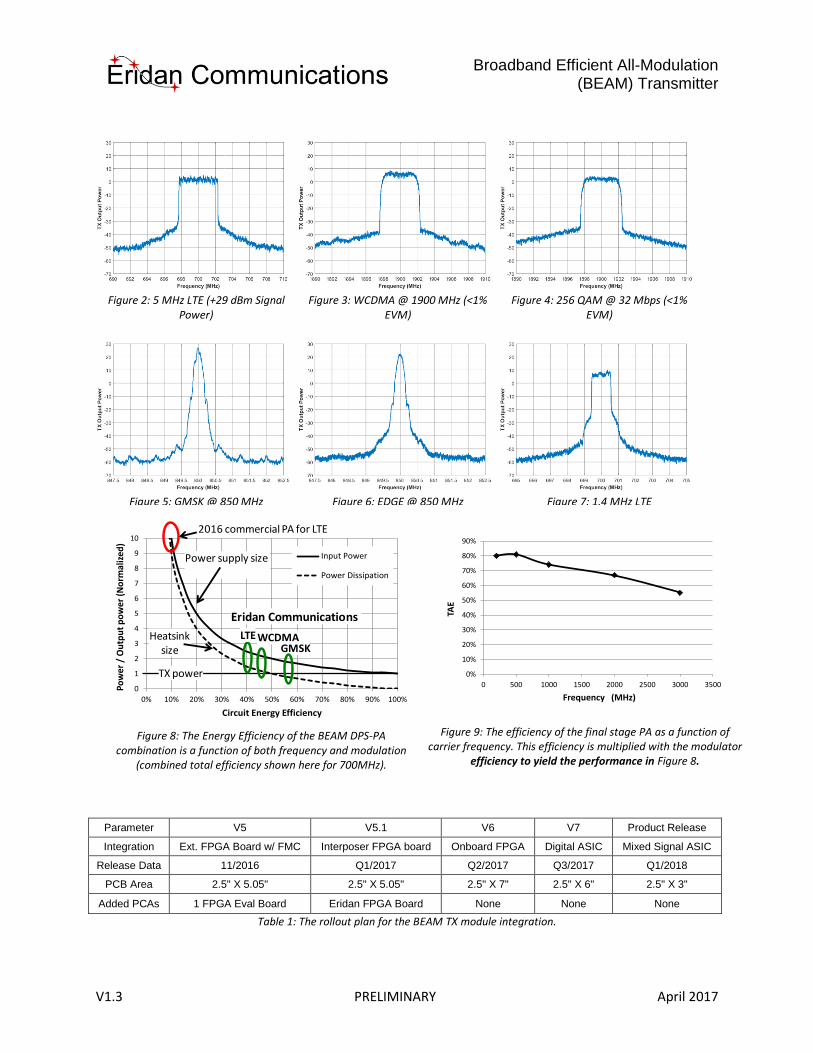
Parameter V5 V5.1 V6 V7 Product Release
Integration Ext. FPGA Board w/ FMC Interposer FPGA board Onboard FPGA Digital ASIC Mixed Signal ASIC
Release Data 11/2016 Q1/2017 Q2/2017 Q3/2017 Q1/2018
PCB Area 2.5" X 5.05" 2.5" X 5.05" 2.5" X 7" 2.5" X 6" 2.5" X 3"
Added PCAs 1 FPGA Eval Board Eridan FPGA Board None None None
Table 1: The rollout plan for the BEAM TX module integration.
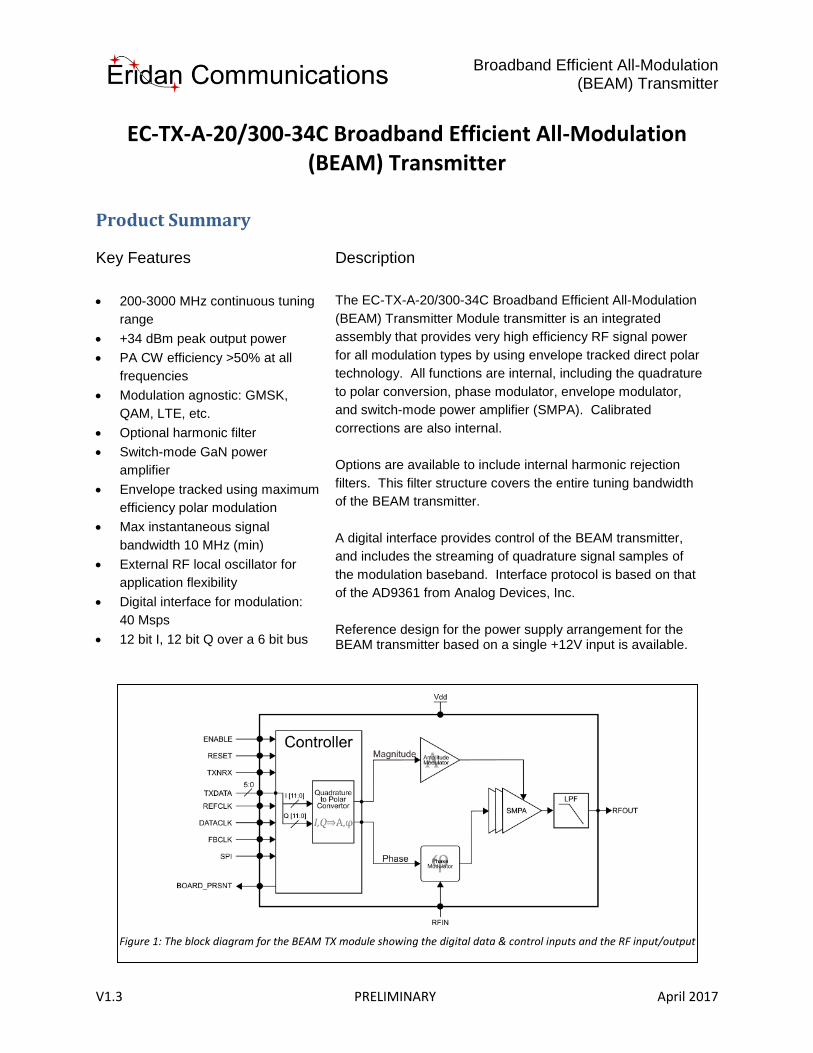
Figure 2: 5 MHz LTE (+29 dBm Signal Power)
Figure 3: WCDMA @ 1900 MHz (<1% EVM)
Figure 4: 256 QAM @ 32 Mbps (<1% EVM)
Figure 5: GMSK @ 850 MHz Figure 6: EDGE @ 850 MHz Figure 7: 1.4 MHz LTE
0
1
2
3
4
5
6
7
8
9
10
0% 10% 20% 30% 40% 50% 60% 70% 80% 90% 100%
Pow
er /
Ou
tpu
t p
ow
er (
No
rmal
ized
)
Circuit Energy Efficiency
Input Power
Power Dissipation
Power supply size
Heatsinksize
2016 commercial PA for LTE
Eridan Communications
TX power
LTE WCDMAGMSK
Figure 8: The Energy Efficiency of the BEAM DPS-PA
combination is a function of both frequency and modulation (combined total efficiency shown here for 700MHz).
0%
10%
20%
30%
40%
50%
60%
70%
80%
90%
0 500 1000 1500 2000 2500 3000 3500
TAE
Frequency (MHz)
Figure 9: The efficiency of the final stage PA as a function of carrier frequency. This efficiency is multiplied with the modulator
efficiency to yield the performance in Figure 8.
Broadband Efficient All-Modulation
(BEAM) Transmitter
V1.3 PRELIMINARY April 2017
Specifications
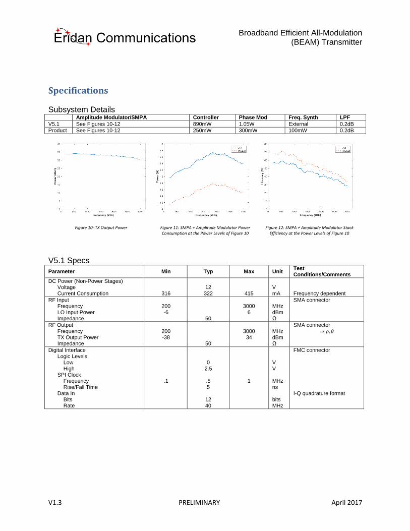
Subsystem Details Amplitude Modulator/SMPA Controller Phase Mod Freq. Synth LPF
V5.1 See Figures 10-12 890mW 1.05W External 0.2dB
Product See Figures 10-12 250mW 300mW 100mW 0.2dB
V5.1 Specs
Parameter Min Typ Max Unit Test Conditions/Comments
DC Power (Non-Power Stages) Voltage Current Consumption
316
12 322
415
V mA
Frequency dependent
RF Input Frequency
LO Input Power Impedance
200 -6
50
3000
6
MHz dBm Ω
SMA connector
RF Output Frequency
TX Output Power Impedance
200 -38
50
3000 34
MHz dBm Ω
SMA connector ⇒ 𝜌, 𝜃
Digital Interface Logic Levels
Low High SPI Clock Frequency Rise/Fall Time Data In Bits Rate
.1
0
2.5
.5 5
12 40
1
V V MHz ns bits MHz
FMC connector I-Q quadrature format
Figure 10: TX Output Power
Figure 11: SMPA + Amplitude Modulator Power Consumption at the Power Levels of Figure 10
Figure 12: SMPA + Amplitude Modulator Stack Efficiency at the Power Levels of Figure 10
Broadband Efficient All-Modulation
(BEAM) Transmitter
V1.3 PRELIMINARY April 2017
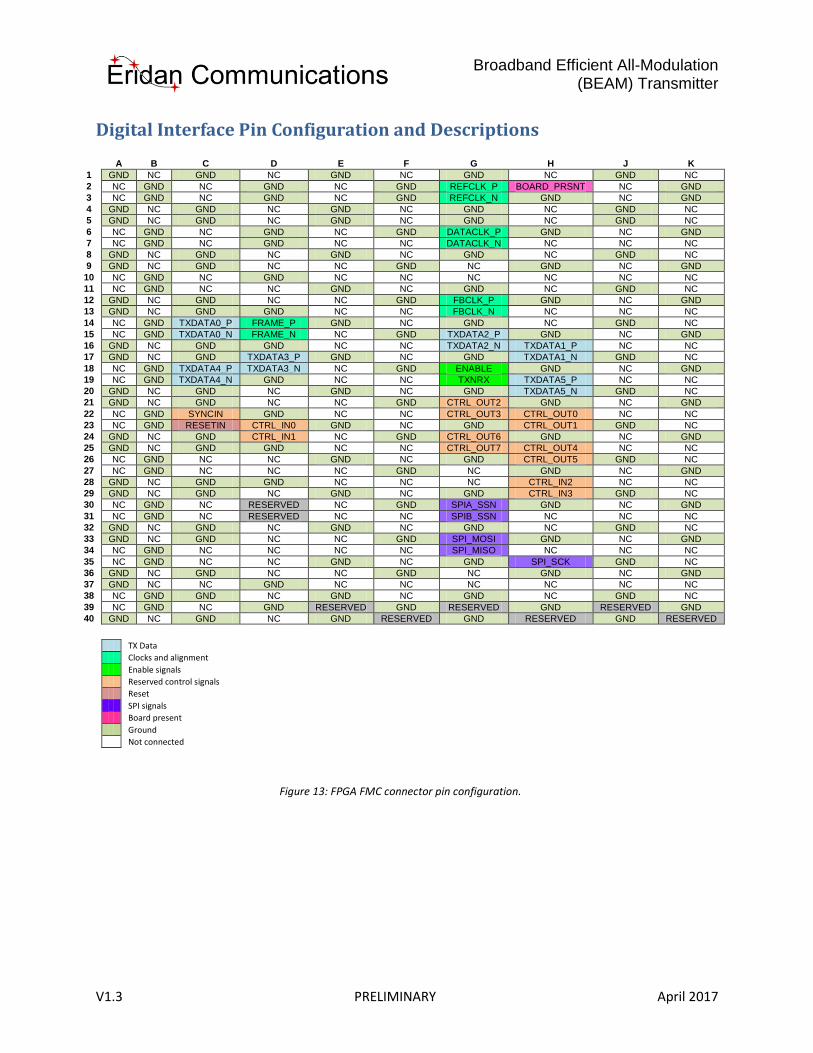
Digital Interface Pin Configuration and Descriptions
A B C D E F G H J K
1 GND NC GND NC GND NC GND NC GND NC
2 NC GND NC GND NC GND REFCLK_P BOARD_PRSNT NC GND
3 NC GND NC GND NC GND REFCLK_N GND NC GND
4 GND NC GND NC GND NC GND NC GND NC
5 GND NC GND NC GND NC GND NC GND NC
6 NC GND NC GND NC GND DATACLK_P GND NC GND
7 NC GND NC GND NC NC DATACLK_N NC NC NC
8 GND NC GND NC GND NC GND NC GND NC
9 GND NC GND NC NC GND NC GND NC GND
10 NC GND NC GND NC NC NC NC NC NC
11 NC GND NC NC GND NC GND NC GND NC
12 GND NC GND NC NC GND FBCLK_P GND NC GND
13 GND NC GND GND NC NC FBCLK_N NC NC NC
14 NC GND TXDATA0_P FRAME_P GND NC GND NC GND NC
15 NC GND TXDATA0_N FRAME_N NC GND TXDATA2_P GND NC GND
16 GND NC GND GND NC NC TXDATA2_N TXDATA1_P NC NC
17 GND NC GND TXDATA3_P GND NC GND TXDATA1_N GND NC
18 NC GND TXDATA4_P TXDATA3_N NC GND ENABLE GND NC GND
19 NC GND TXDATA4_N GND NC NC TXNRX TXDATA5_P NC NC
20 GND NC GND NC GND NC GND TXDATA5_N GND NC
21 GND NC GND NC NC GND CTRL_OUT2 GND NC GND
22 NC GND SYNCIN GND NC NC CTRL_OUT3 CTRL_OUT0 NC NC
23 NC GND RESETIN CTRL_IN0 GND NC GND CTRL_OUT1 GND NC
24 GND NC GND CTRL_IN1 NC GND CTRL_OUT6 GND NC GND
25 GND NC GND GND NC NC CTRL_OUT7 CTRL_OUT4 NC NC
26 NC GND NC NC GND NC GND CTRL_OUT5 GND NC
27 NC GND NC NC NC GND NC GND NC GND
28 GND NC GND GND NC NC NC CTRL_IN2 NC NC
29 GND NC GND NC GND NC GND CTRL_IN3 GND NC
30 NC GND NC RESERVED NC GND SPIA_SSN GND NC GND
31 NC GND NC RESERVED NC NC SPIB_SSN NC NC NC
32 GND NC GND NC GND NC GND NC GND NC
33 GND NC GND NC NC GND SPI_MOSI GND NC GND
34 NC GND NC NC NC NC SPI_MISO NC NC NC
35 NC GND NC NC GND NC GND SPI_SCK GND NC
36 GND NC GND NC NC GND NC GND NC GND
37 GND NC NC GND NC NC NC NC NC NC
38 NC GND GND NC GND NC GND NC GND NC
39 NC GND NC GND RESERVED GND RESERVED GND RESERVED GND
40 GND NC GND NC GND RESERVED GND RESERVED GND RESERVED
TX Data
Clocks and alignment
Enable signals
Reserved control signals
Reset
SPI signals
Board present
Ground
Not connected
Figure 13: FPGA FMC connector pin configuration.
Broadband Efficient All-Modulation
(BEAM) Transmitter
V1.3 PRELIMINARY April 2017
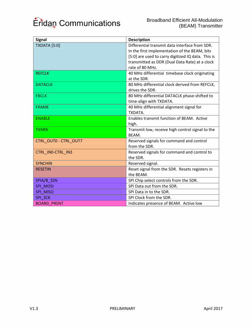
Signal Description
TXDATA [5:0] Differential transmit data interface from SDR. In the first implementation of the BEAM, bits [5:0] are used to carry digitized IQ data. This is transmitted as DDR (Dual Data Rate) at a clock rate of 80 MHz.
REFCLK 40 MHz differential timebase clock originating at the SDR.
DATACLK 80 MHz differential clock derived from REFCLK, drives the SDR.
FBCLK 80 MHz differential DATACLK phase-shifted to time-align with TXDATA.
FRAME 40 MHz differential alignment signal for TXDATA.
ENABLE Enables transmit function of BEAM. Active high.
TXNRX Transmit low, receive high control signal to the BEAM.
CTRL_OUT0 - CTRL_OUT7 Reserved signals for command and control from the SDR.
CTRL_IN0-CTRL_IN3 Reserved signals for command and control to the SDR.
SYNCHIN Reserved signal.
RESETIN Reset signal from the SDR. Resets registers in the BEAM.
SPIA/B_SSN SPI Chip select controls from the SDR.
SPI_MOSI SPI Data out from the SDR.
SPI_MISO SPI Data in to the SDR.
SPI_SCK SPI Clock from the SDR.
BOARD_PRSNT Indicates presence of BEAM. Active low
Broadband Efficient All-Modulation
(BEAM) Transmitter
V1.3 PRELIMINARY April 2017
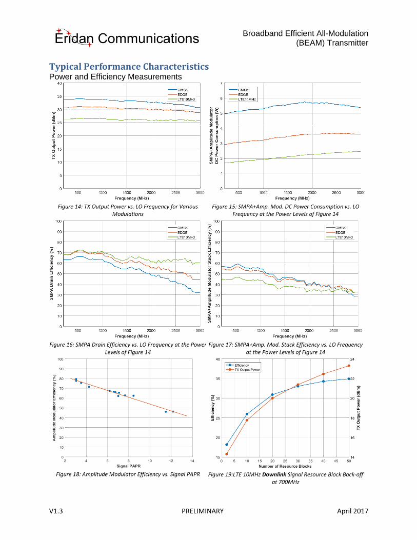
Typical Performance Characteristics Power and Efficiency Measurements
Figure 14: TX Output Power vs. LO Frequency for Various Modulations
Figure 15: SMPA+Amp. Mod. DC Power Consumption vs. LO Frequency at the Power Levels of Figure 14
Figure 16: SMPA Drain Efficiency vs. LO Frequency at the Power Levels of Figure 14
Figure 17: SMPA+Amp. Mod. Stack Efficiency vs. LO Frequency at the Power Levels of Figure 14
Figure 18: Amplitude Modulator Efficiency vs. Signal PAPR Figure 19:LTE 10MHz Downlink Signal Resource Block Back-off at 700MHz
Broadband Efficient All-Modulation
(BEAM) Transmitter
V1.3 PRELIMINARY April 2017
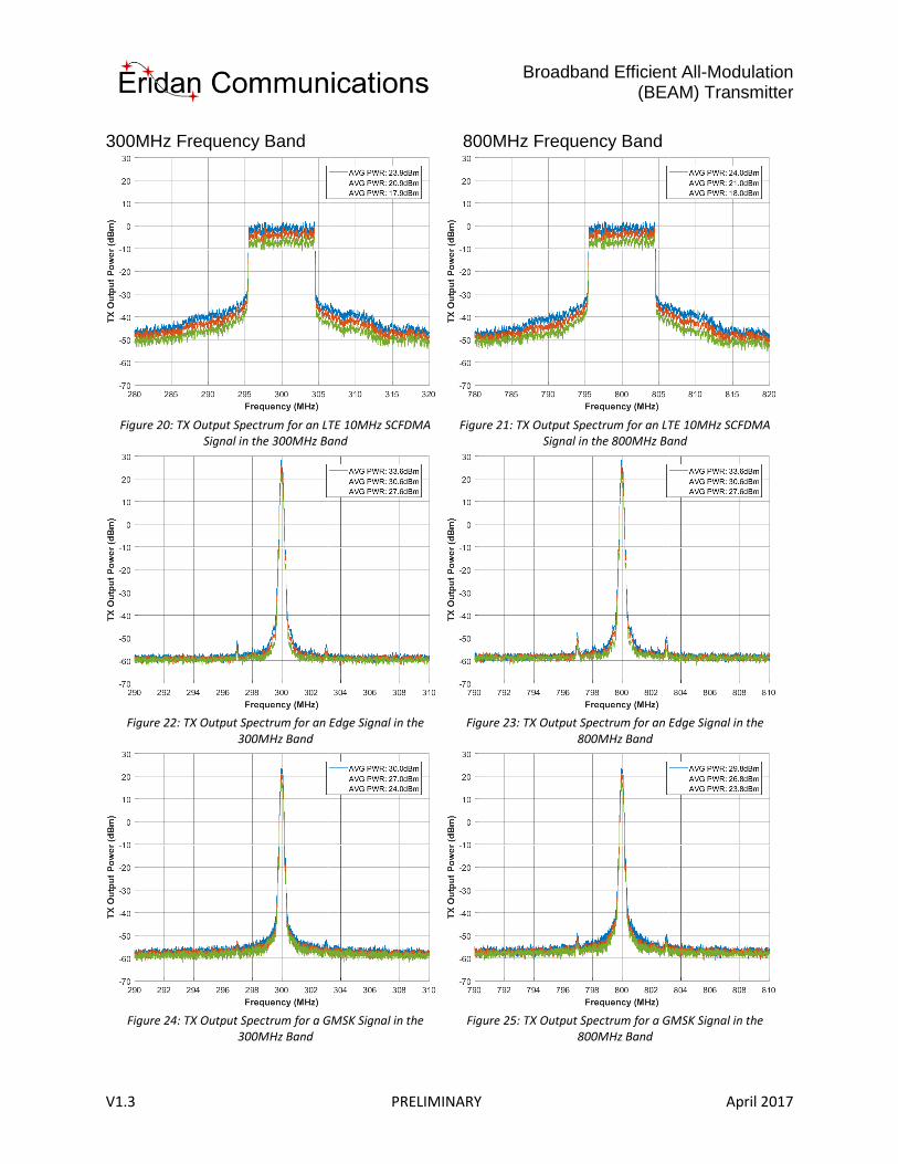
300MHz Frequency Band 800MHz Frequency Band
Figure 20: TX Output Spectrum for an LTE 10MHz SCFDMA Signal in the 300MHz Band
Figure 21: TX Output Spectrum for an LTE 10MHz SCFDMA Signal in the 800MHz Band
Figure 22: TX Output Spectrum for an Edge Signal in the 300MHz Band
Figure 23: TX Output Spectrum for an Edge Signal in the 800MHz Band
Figure 24: TX Output Spectrum for a GMSK Signal in the 300MHz Band
Figure 25: TX Output Spectrum for a GMSK Signal in the 800MHz Band
Broadband Efficient All-Modulation
(BEAM) Transmitter
V1.3 PRELIMINARY April 2017
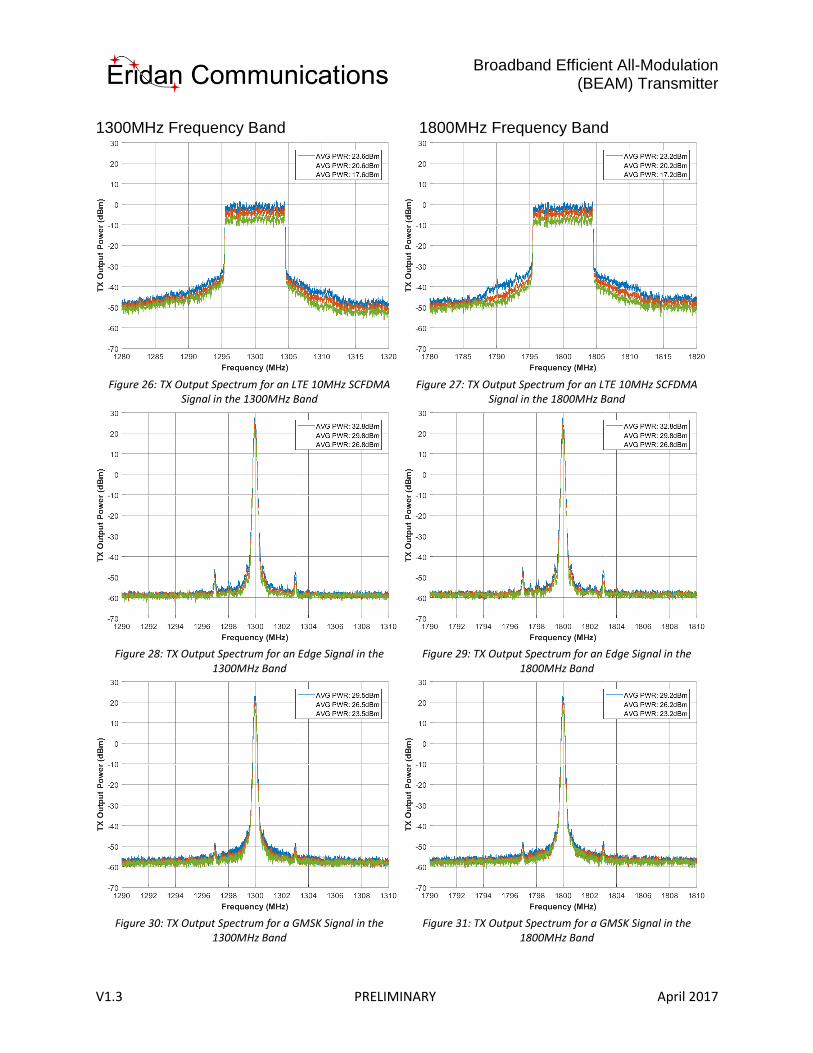
1300MHz Frequency Band 1800MHz Frequency Band
Figure 26: TX Output Spectrum for an LTE 10MHz SCFDMA Signal in the 1300MHz Band
Figure 27: TX Output Spectrum for an LTE 10MHz SCFDMA Signal in the 1800MHz Band
Figure 28: TX Output Spectrum for an Edge Signal in the 1300MHz Band
Figure 29: TX Output Spectrum for an Edge Signal in the 1800MHz Band
Figure 30: TX Output Spectrum for a GMSK Signal in the 1300MHz Band
Figure 31: TX Output Spectrum for a GMSK Signal in the 1800MHz Band
Broadband Efficient All-Modulation
(BEAM) Transmitter
V1.3 PRELIMINARY April 2017
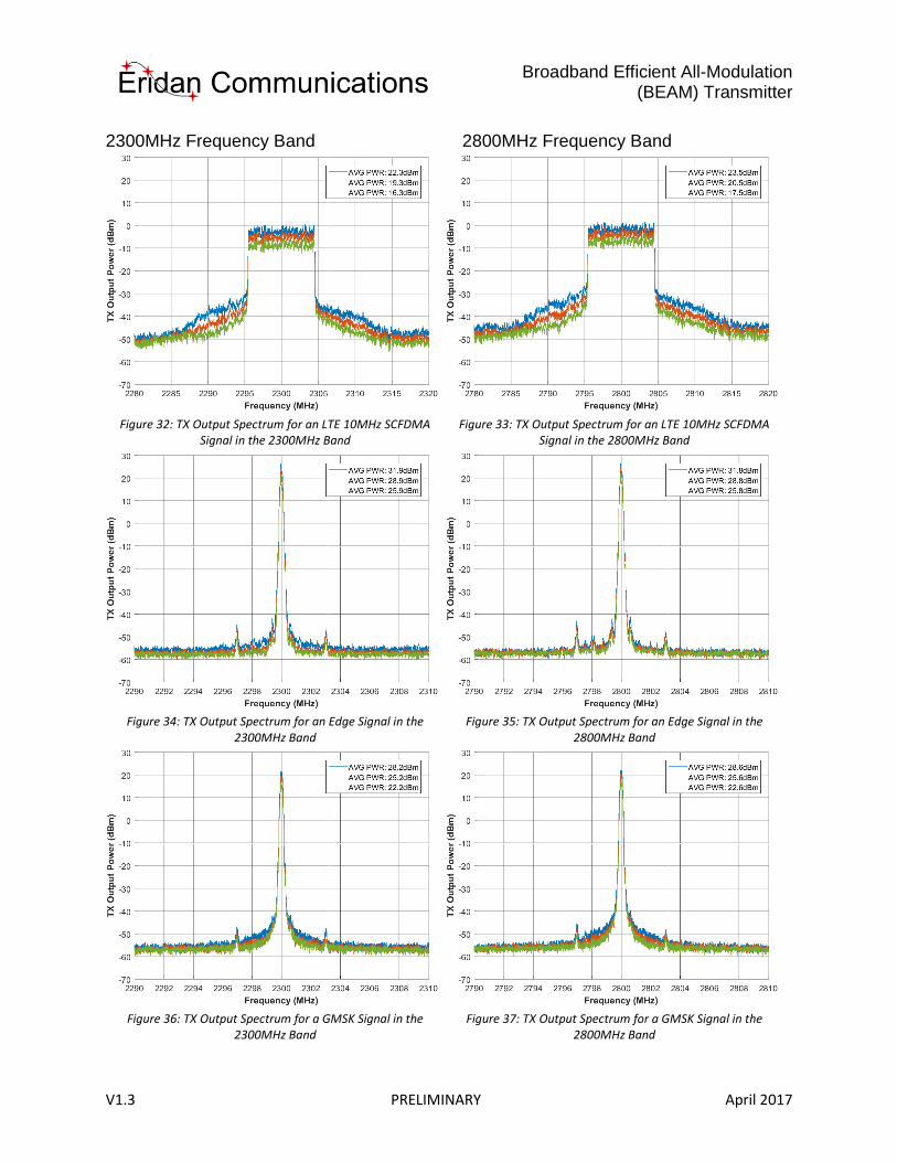
2300MHz Frequency Band 2800MHz Frequency Band
Figure 32: TX Output Spectrum for an LTE 10MHz SCFDMA Signal in the 2300MHz Band
Figure 33: TX Output Spectrum for an LTE 10MHz SCFDMA Signal in the 2800MHz Band
Figure 34: TX Output Spectrum for an Edge Signal in the 2300MHz Band
Figure 35: TX Output Spectrum for an Edge Signal in the 2800MHz Band
Figure 36: TX Output Spectrum for a GMSK Signal in the 2300MHz Band
Figure 37: TX Output Spectrum for a GMSK Signal in the 2800MHz Band
Broadband Efficient All-Modulation
(BEAM) Transmitter
V1.3 PRELIMINARY April 2017
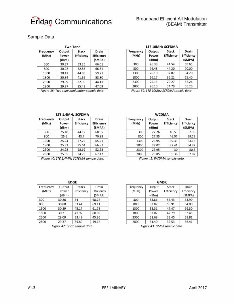
Sample Data
WCDMA Frequency
(MHz) Output Power (dBm)
Stack Efficiency
Drain Efficiency (SMPA)
300 27.26 46.53 67.38
800 27.35 46.07 69.29
1300 26.95 39.33 63.18
1800 27.02 37.41 64.32
2300 25.95 30 50.3
2800 26.85 35.36 62.02
Figure 41: WCDMA sample data.
LTE 1.4MHz SCFDMA Frequency
(MHz) Output Power (dBm)
Stack Efficiency
Drain Efficiency (SMPA)
300 25.48 44.12 68.95
800 25.6 43.7 70.85
1300 25.24 37.25 65.21
1800 25.33 35.64 66.87
2300 24.28 28.69 52.58
2800 25.35 34.73 67.42
Figure 40: LTE 1.4MHz SCFDMA sample data.
GMSK Frequency
(MHz) Output Power (dBm)
Stack Efficiency
Drain Efficiency (SMPA)
300 33.86 56.43 63.90
800 33.87 55.91 64.00
1300 33.31 47.47 56.30
1800 33.07 42.79 53.45
2300 31.68 33.45 38.81
2800 31.40 32.53 36.41
Figure 43: GMSK sample data.
Two Tone Frequency
(MHz) Output Power (dBm)
Stack Efficiency
Drain Efficiency (SMPA)
300 30.87 53.25 66.01
800 30.92 52.85 66.51
1300 30.41 44.83 59.71
1800 30.34 41.69 58.80
2300 29.09 32.95 44.11
2800 29.37 35.43 47.09
Figure 38: Two-tone modulation sample data.
LTE 10MHz SCFDMA Frequency
(MHz) Output Power (dBm)
Stack Efficiency
Drain Efficiency (SMPA)
300 26.38 44.54 69.65
800 26.48 44.20 70.00
1300 26.10 37.87 64.20
1800 26.17 36.21 65.40
2300 25.15 29.27 52.24
2800 26.10 34.79 65.26
Figure 39: LTE 10MHz SCFDMAsample data.
EDGE Frequency
(MHz) Output Power (dBm)
Stack Efficiency
Drain Efficiency (SMPA)
300 30.86 54 68.72
800 30.88 53.44 69.11
1300 30.39 45.17 61.78
1800 30.3 41.92 60.69
2300 29.08 33.42 45.86
2800 29.37 35.89 49.12
Figure 42: EDGE sample data.