Embed Size (px)
Citation preview
Lecture Notes Prepared by Amir G. Aghdam
1
`COEN 312 DIGITAL SYSTEMS DESIGN - LECTURE NOTES
Concordia University
Chapter 5: Synchronous Sequential Logic
NOTE: For more examples and detailed description of the material in the lecture notes, please refer to the main textbook: Digital Design 3rd Edition, By Morris Mano, Publisher Prentice Hall, 4th Edition All examples used in the lecture notes are from the above reference. Sequential Circuits
- A sequential circuit consists of a combinational circuit and a feedback through the
storage elements in the circuit.
- Sequential circuits can be categorized as being synchronous or asynchronous.
- A synchronous sequential circuit usually has a clock pulse (clocked sequential
circuits).
- Flip-flops are storage elements which are used in clocked sequential circuits.
- Each flip-flop can store one bit.
- A synchronous clocked sequential circuit is shown below:
Latches
- Latches are the basic types of flip-flops.
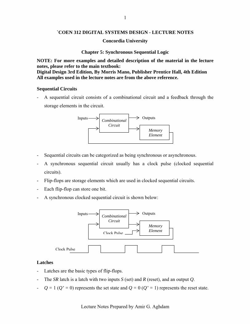
- The SR latch is a latch with two inputs S (set) and R (reset), and an output Q.
- Q = 1 (Q’ = 0) represents the set state and Q = 0 (Q’ = 1) represents the reset state.
Combinational Circuit
Outputs Inputs
Memory Element
Combinational Circuit
Outputs Inputs
Memory Element Clock Pulse
Clock Pulse
Lecture Notes Prepared by Amir G. Aghdam
2
- The SR latch can be implemented by NOR gates or NAND gates.
- Assume S=1 and R=0 in the above circuit. Then the output of the bottom gate (Q’) is
definitely 0 (note that the output of a NOR gate is zero if at least one of its inputs is
1). This means that the output of the top gate (Q) is 1, as both of its inputs are 0. This
is called the set state.
- Assume now that right after the above state, S becomes 0. Since from the previous
state we have Q=1, hence the output of the bottom gate stays at 0 and consequently
the output of the top gate also stays at 1, as both of its inputs are equal to 0.
- Similarly, if S=0 and R=1, then we will have Q=0 and Q’=1, which is the reset state
(this can be concluded from the symmetrical configuration of the circuit as well).
Again, if R becomes 0 right after the reset state, the outputs will remain unchanged
(Q=0 and Q’=1).
- After any change in the input, it has to go to zero so that the circuit becomes ready for
the next state.
- In undefined state the next output is not predictable when both inputs go back to zero
(it depends whether the S or R input goes to zero first).
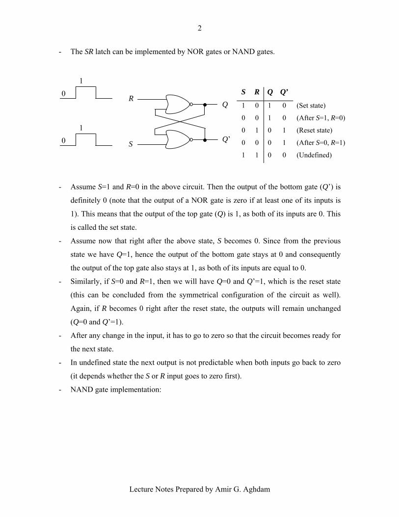
- NAND gate implementation:
S R Q Q’
1 0 1 0 (Set state)
0 0 1 0 (After S=1, R=0)
0 1 0 1 (Reset state)
0 0 0 1 (After S=0, R=1)
1 1 0 0 (Undefined)
1
1
0
0 R
S
Q
Q’
Lecture Notes Prepared by Amir G. Aghdam
3
- Assume S=0 and R=1 in the above circuit. Then the output of the top gate (Q) is
definitely 1 (note that the output of a NAND gate is 1 if at least one of its inputs is 0).
This means that the output of the bottom gate (Q’) is 0, as both of its inputs are 1.
- Assume now that right after the above state, S becomes 1. Since from the previous
state we have Q=1, hence the output of the bottom gate stays at 0 and consequently
the output of the top gate also stays at 1, as one of its inputs is equal to 0.
- One should make sure that both inputs are not connected to zero simultaneously.
- SR latch with control input is shown below:
- D latch (data latch) is an element which holds data in its internal storage and the
output becomes equal to D each time C enables the circuit (by changing to 1).
S R Q Q’
1 0 0 1
1 1 0 1 (After S=1, R=0)
0 1 1 0
1 1 1 0 (After S=0, R=1)
0 0 1 1 (Undefined)
C S R Next state of Q
0 x x No change
1 0 0 No change
1 0 1 Q=0 (Reset state)
1 1 0 Q=1 (Set state)
1 1 1 Undefined
S
R
Q
Q’
Q
Q’
S
C (Control input)
R
Lecture Notes Prepared by Amir G. Aghdam
4
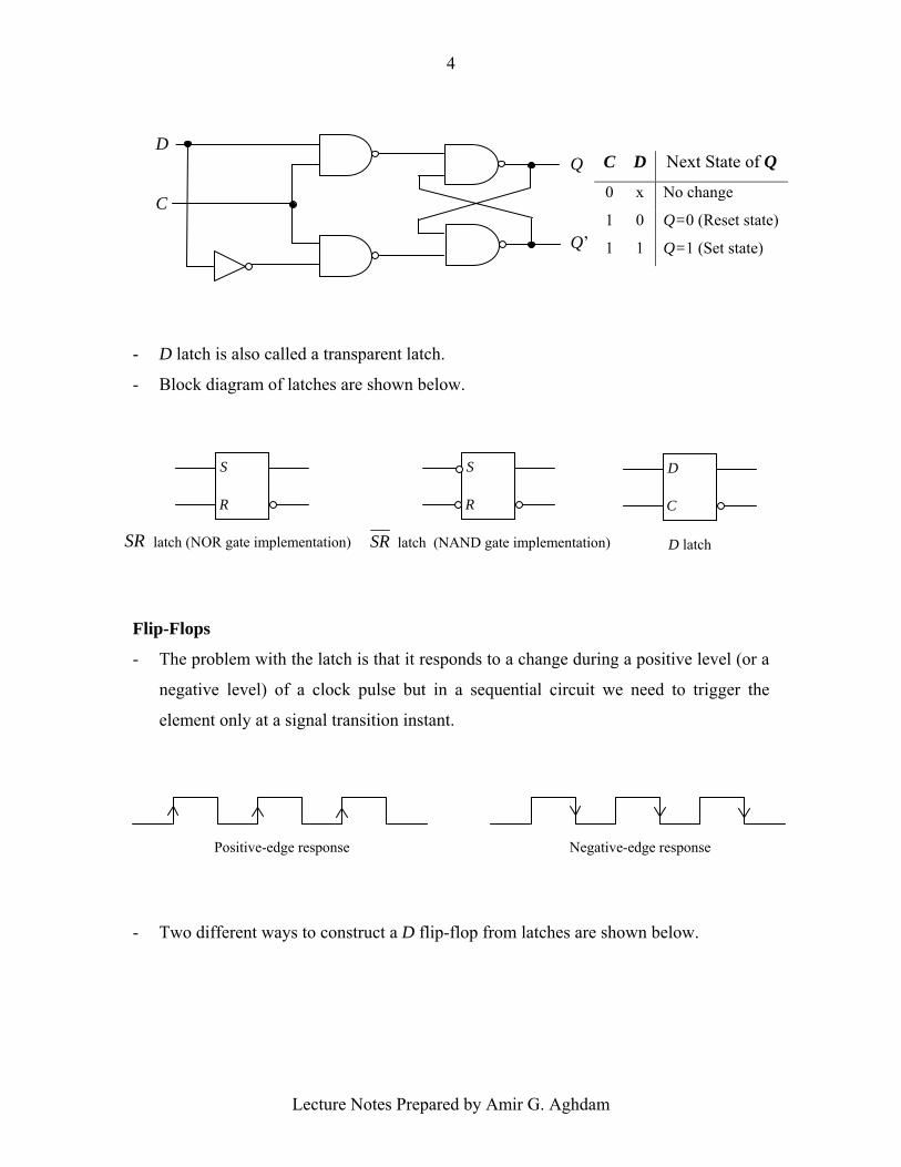
- D latch is also called a transparent latch.
- Block diagram of latches are shown below.
Flip-Flops
- The problem with the latch is that it responds to a change during a positive level (or a
negative level) of a clock pulse but in a sequential circuit we need to trigger the
element only at a signal transition instant.
- Two different ways to construct a D flip-flop from latches are shown below.
C D Next State of Q
0 x No change
1 0 Q=0 (Reset state)
1 1 Q=1 (Set state)
SR latch (NOR gate implementation)
S
R
S
R
SR latch (NAND gate implementation)
D
C
D latch
Q
Q’
D
C
Positive-edge response Negative-edge response
Lecture Notes Prepared by Amir G. Aghdam
5
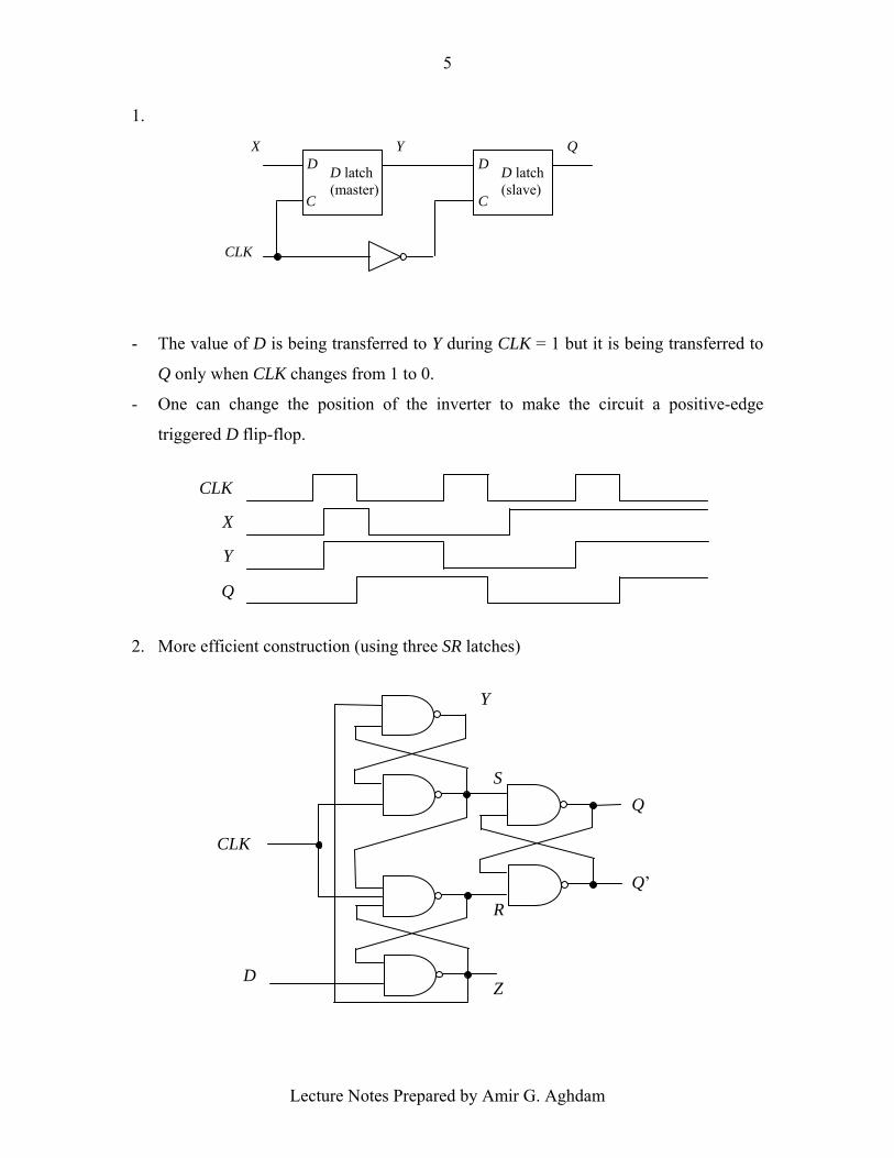
1.
- The value of D is being transferred to Y during CLK = 1 but it is being transferred to
Q only when CLK changes from 1 to 0.
- One can change the position of the inverter to make the circuit a positive-edge
triggered D flip-flop.
2. More efficient construction (using three SR latches)
D
C
D
C
Y QX
CLK
D latch (master)
D latch (slave)
Q
Q’
S
CLK
R
Z
Y
D
Q
Y
X
CLK
Lecture Notes Prepared by Amir G. Aghdam
6
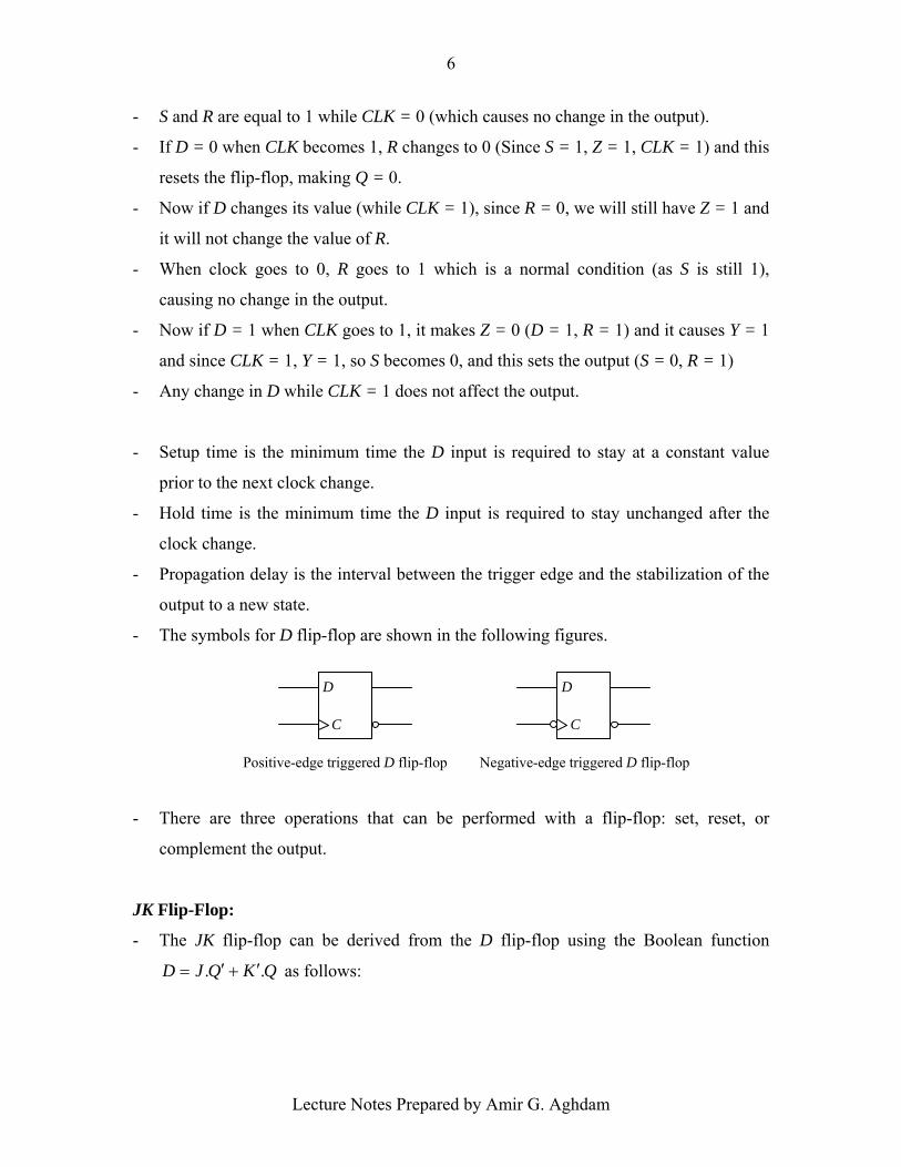
- S and R are equal to 1 while CLK = 0 (which causes no change in the output).
- If D = 0 when CLK becomes 1, R changes to 0 (Since S = 1, Z = 1, CLK = 1) and this
resets the flip-flop, making Q = 0.
- Now if D changes its value (while CLK = 1), since R = 0, we will still have Z = 1 and
it will not change the value of R.
- When clock goes to 0, R goes to 1 which is a normal condition (as S is still 1),
causing no change in the output.
- Now if D = 1 when CLK goes to 1, it makes Z = 0 (D = 1, R = 1) and it causes Y = 1
and since CLK = 1, Y = 1, so S becomes 0, and this sets the output (S = 0, R = 1)
- Any change in D while CLK = 1 does not affect the output.
- Setup time is the minimum time the D input is required to stay at a constant value
prior to the next clock change.
- Hold time is the minimum time the D input is required to stay unchanged after the
clock change.
- Propagation delay is the interval between the trigger edge and the stabilization of the
output to a new state.
- The symbols for D flip-flop are shown in the following figures.
- There are three operations that can be performed with a flip-flop: set, reset, or
complement the output.
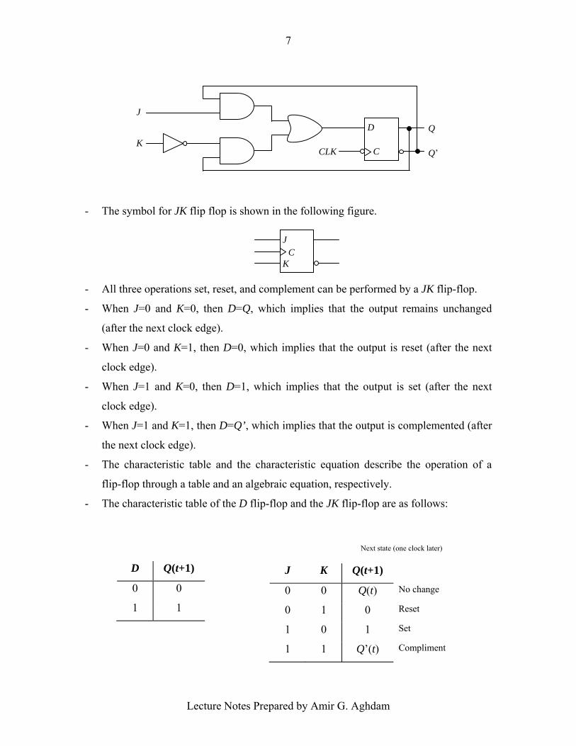
JK Flip-Flop:
- The JK flip-flop can be derived from the D flip-flop using the Boolean function
QKQJD .. ′+′= as follows:
D
C
D
C
Positive-edge triggered D flip-flop Negative-edge triggered D flip-flop
Lecture Notes Prepared by Amir G. Aghdam
7
- The symbol for JK flip flop is shown in the following figure.
- All three operations set, reset, and complement can be performed by a JK flip-flop.
- When J=0 and K=0, then D=Q, which implies that the output remains unchanged
(after the next clock edge).
- When J=0 and K=1, then D=0, which implies that the output is reset (after the next
clock edge).
- When J=1 and K=0, then D=1, which implies that the output is set (after the next
clock edge).
- When J=1 and K=1, then D=Q’, which implies that the output is complemented (after
the next clock edge).
- The characteristic table and the characteristic equation describe the operation of a
flip-flop through a table and an algebraic equation, respectively.
- The characteristic table of the D flip-flop and the JK flip-flop are as follows:
Next state (one clock later)
J K Q(t+1)
0 0 Q(t) No change
0 1 0 Reset
1 0 1 Set
1 1 Q’(t) Compliment
D Q(t+1)
0 0
1 1
J
KC
D
CCLK
J
K Q
Q’
Lecture Notes Prepared by Amir G. Aghdam
8
- The characteristic equation of the D flip-flop and the JK flip-flop are as follows:
Q(t+1)=D , Q(t+1)=J.Q’(t)+K’.Q(t)
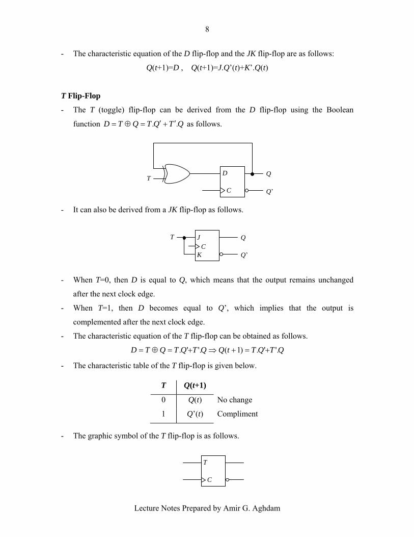
T Flip-Flop
- The T (toggle) flip-flop can be derived from the D flip-flop using the Boolean
function QTQTQTD .. ′+′=⊕= as follows.
- It can also be derived from a JK flip-flop as follows.
- When T=0, then D is equal to Q, which means that the output remains unchanged
after the next clock edge.
- When T=1, then D becomes equal to Q’, which implies that the output is
complemented after the next clock edge.
- The characteristic equation of the T flip-flop can be obtained as follows.
QTQTtQQTQTQTD '.'.)1('.'. +=+⇒+=⊕=
- The characteristic table of the T flip-flop is given below.
- The graphic symbol of the T flip-flop is as follows.
T Q(t+1)
0 Q(t) No change
1 Q’(t) Compliment
J
KC
T
Q’
Q
T Q
Q’
D
C
T
C
Lecture Notes Prepared by Amir G. Aghdam
9
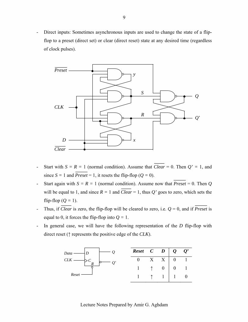
- Direct inputs: Sometimes asynchronous inputs are used to change the state of a flip-
flop to a preset (direct set) or clear (direct reset) state at any desired time (regardless
of clock pulses).
- Start with S = R = 1 (normal condition). Assume that Clear = 0. Then Q’ = 1, and
since S = 1 and Preset = 1, it resets the flip-flop (Q = 0).
- Start again with S = R = 1 (normal condition). Assume now that Preset = 0. Then Q
will be equal to 1, and since R = 1 and Clear = 1, thus Q’ goes to zero, which sets the
flip-flop (Q = 1).
- Thus, if Clear is zero, the flip-flop will be cleared to zero, i.e. Q = 0, and if Preset is
equal to 0, it forces the flip-flop into Q = 1.
- In general case, we will have the following representation of the D flip-flop with
direct reset (↑ represents the positive edge of the CLK).
Reset C D Q Q’
0
1
1
X
↑
↑
X
0
1
0
0
1
1
1
0
D
Preset
Clear
R
S Q
Q’
CLK
x
y
D
C
Q
Q’
Data CLK
Reset
R

Lecture Notes Prepared by Amir G. Aghdam
10
Analysis of Clocked Sequential Circuits
- A clocked sequential circuit can be analyzed by using: (i) The state equation obtained
by replacing flip-flop input equations in its characteristic equation, or (ii) a state table.
- Analysis with D flip-flops: Write the Boolean expression for each flip-flop input,
which is, in fact, the flip-flop output right after the next active clock edge.
- Example:
- State equation can be written as:
)().()1()().()().()1(
txtAtBtxtBtxtAtA
′=++=+
- or simply:
xAtBxBxAtA
.)1(..)1(
′=++=+
- The output is given by:
)()].()([)( txtBtAty ′+=
- or simply:
xBAy ′+= ].[
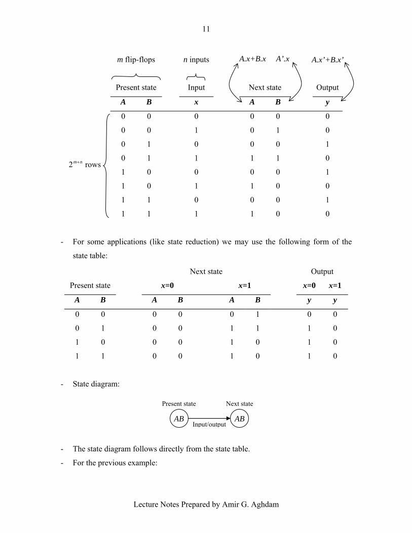
- State table or transition table lists all possible binary combinations of present state
and inputs.
D
CLK
x
A
A’
D
C
C
B
B’
y
Lecture Notes Prepared by Amir G. Aghdam
11
- For some applications (like state reduction) we may use the following form of the
state table:
- State diagram:
- The state diagram follows directly from the state table.
- For the previous example:
m flip-flops n inputs
Present state Input Next state Output
A B x A B y
0 0 0 0 0 0
0 0 1 0 1 0
0 1 0 0 0 1
0 1 1 1 1 0
1 0 0 0 0 1
1 0 1 1 0 0
1 1 0 0 0 1
1 1 1 1 0 0
Next state Output
Present state x=0 x=1 x=0 x=1
A B A B A B y y
0 0 0 0 0 1 0 0
0 1 0 0 1 1 1 0
1 0 0 0 1 0 1 0
1 1 0 0 1 0 1 0
A.x’+B.x’A.x+B.x A’.x
rows 2 nm+
AB ABInput/output
Present state Next state
Lecture Notes Prepared by Amir G. Aghdam
12
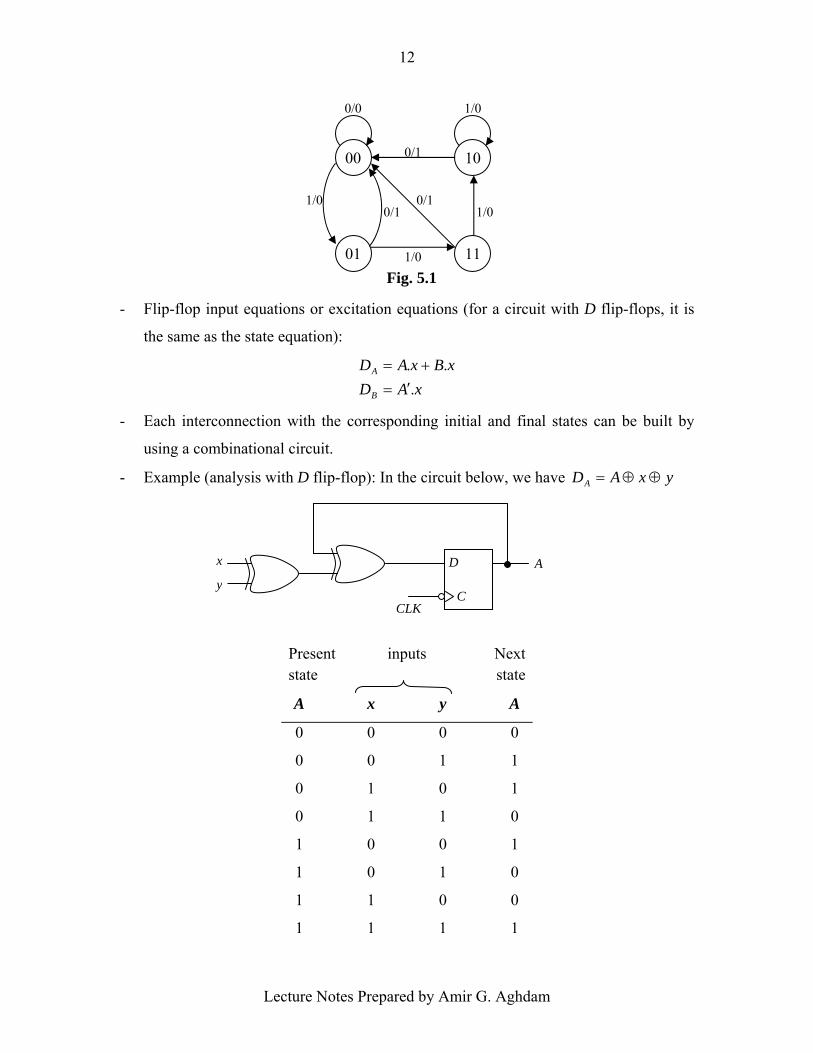
- Flip-flop input equations or excitation equations (for a circuit with D flip-flops, it is
the same as the state equation):
xADxBxAD
B
A
...
′=+=
- Each interconnection with the corresponding initial and final states can be built by
using a combinational circuit.
- Example (analysis with D flip-flop): In the circuit below, we have yxADA ⊕⊕=
Present state
inputs Next state
A x y A
0 0 0 0
0 0 1 1
0 1 0 1
0 1 1 0
1 0 0 1
1 0 1 0
1 1 0 0
1 1 1 1
Fig. 5.1
00 100/1
1/01/0
01 111/0
0/10/1
0/0 1/0
D
C
x Ay
CLK
Lecture Notes Prepared by Amir G. Aghdam
13
- When the output is not specified, we assume that the output is the output of the flip-
flop.
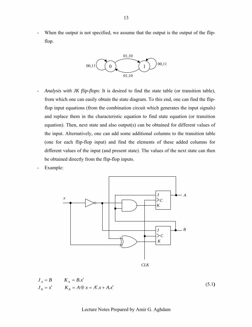
- Analysis with JK flip-flops: It is desired to find the state table (or transition table),
from which one can easily obtain the state diagram. To this end, one can find the flip-
flop input equations (from the combination circuit which generates the input signals)
and replace them in the characteristic equation to find state equation (or transition
equation). Then, next state and also output(s) can be obtained for different values of
the input. Alternatively, one can add some additional columns to the transition table
(one for each flip-flop input) and find the elements of these added columns for
different values of the input (and present state). The values of the next state can then
be obtained directly from the flip-flop inputs.
- Example:
xAxAxAKxJxBKBJ
BB
A
′+′=⊕=′=
′==..
. A
0 1 00,11
01,10
00,11
01,10
J
CLK
x A
J
K
K
B C
C
(5.1)
Lecture Notes Prepared by Amir G. Aghdam
14
- One can also find the next state from the state equations by substituting the input
equations into the flip-flop characteristic equations, as pointed out earlier.
- Characteristic equation for the JK flip-flop is:
⎪⎩
⎪⎨⎧
+′=+
+′=+
BKBJtB
AKAJtA
BB
AA
..)1(
..)1('
'
- Substituting the flip-flop input equations given in (5.1) into the above equations:
⎩⎨⎧
′′++′′=′⊕+′′=++′+′=′′+′=+
⇒xBAxBAxBBxABxtB
xABABAAxBABtA......)(.)1(
....).(.)1( :equations state
- Next states in the table can now be obtained directly (no need for the flip-flop inputs).
Present state Input Next State Flip-Flop inputs
A B x A B AJ AK BJ BK
0 0 0 0 1 0 0 1 0
0 0 1 0 0 0 0 0 1
0 1 0 1 1 1 1 1 0
0 1 1 1 0 1 0 0 1
1 0 0 1 1 0 0 1 1
1 0 1 1 0 0 0 0 0
1 1 0 0 0 1 1 1 1
1 1 1 1 1 1 0 0 0
These are obtained from the boolean
expressions (just like ordinary truth
table) based on the present states.
Note that this is not part of the table.
00 11
01 10
1
1 1
Fig. 5.2
0 0
0
1
Lecture Notes Prepared by Amir G. Aghdam
15
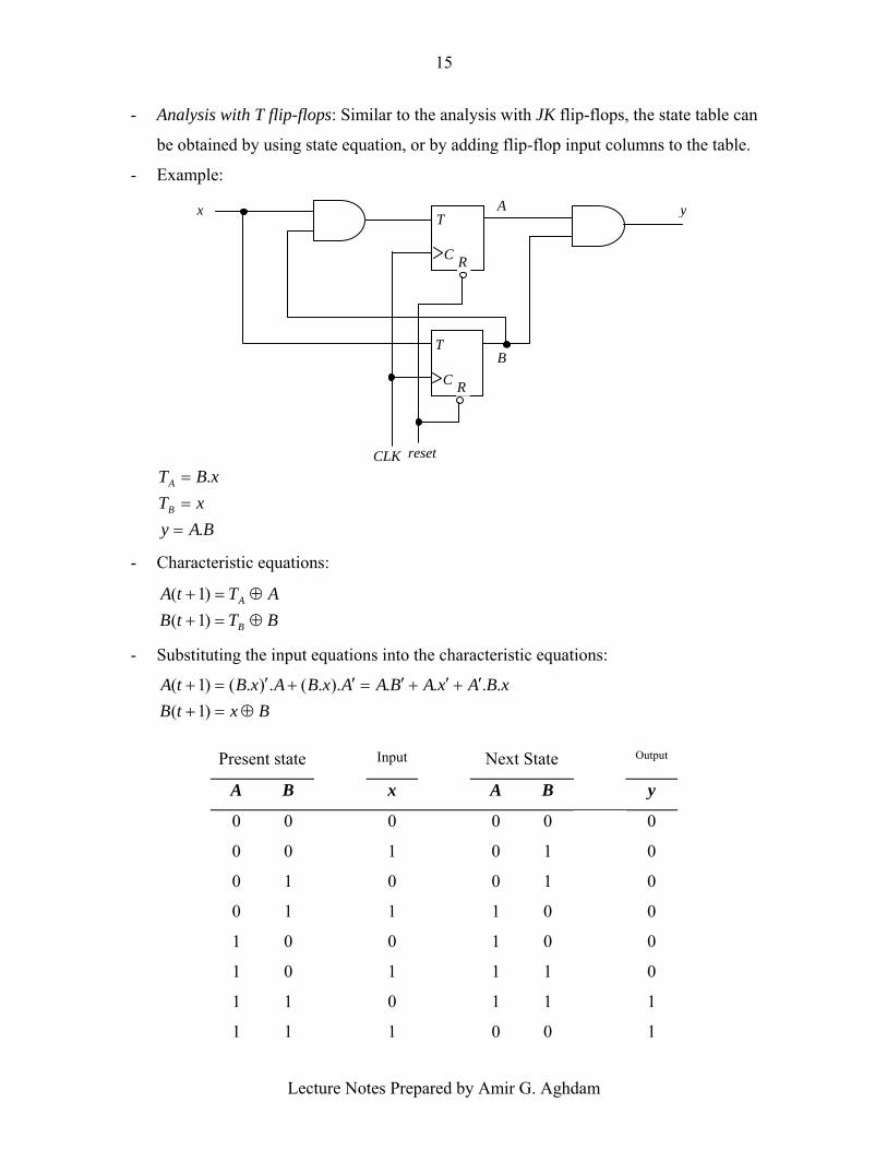
- Analysis with T flip-flops: Similar to the analysis with JK flip-flops, the state table can
be obtained by using state equation, or by adding flip-flop input columns to the table.
- Example:
BAyxT
xBT
B
A
.
.
===
- Characteristic equations:
BTtBATtA
B
A
⊕=+⊕=+
)1()1(
- Substituting the input equations into the characteristic equations:
BxtBxBAxABAAxBAxBtA
⊕=+
′+′+′=′+′=+)1(
....)..(.).()1(
Present state Input Next State Output
A B x A B y
0 0 0 0 0 0
0 0 1 0 1 0
0 1 0 0 1 0
0 1 1 1 0 0
1 0 0 1 0 0
1 0 1 1 1 0
1 1 0 1 1 1
1 1 1 0 0 1
0
CLK
x A y
reset
B
T
C R
T
C R
Lecture Notes Prepared by Amir G. Aghdam
16
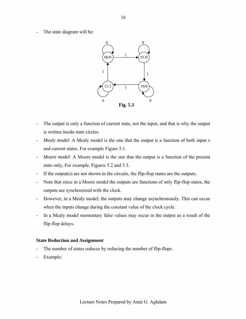
- The state diagram will be:
- The output is only a function of current state, not the input, and that is why the output
is written inside state circles.
- Mealy model: A Mealy model is the one that the output is a function of both input x
and current states. For example Figure 5.1.
- Moore model: A Moore model is the one that the output is a function of the present
state only, For example, Figures 5.2 and 5.3.
- If the output(s) are not shown in the circuits, the flip-flop states are the outputs.
- Note that since in a Moore model the outputs are functions of only flip-flop states, the
outputs are synchronized with the clock.
- However, in a Mealy model, the outputs may change asynchronously. This can occur
when the inputs change during the constant value of the clock cycle.
- In a Mealy model momentary false values may occur in the output as a result of the
flip-flop delays.
State Reduction and Assignment
- The number of states reduces by reducing the number of flip-flops.
- Example:
0 0
00/0 01/01
11
11/1 10/01
0 0Fig. 5.3
Lecture Notes Prepared by Amir G. Aghdam
17
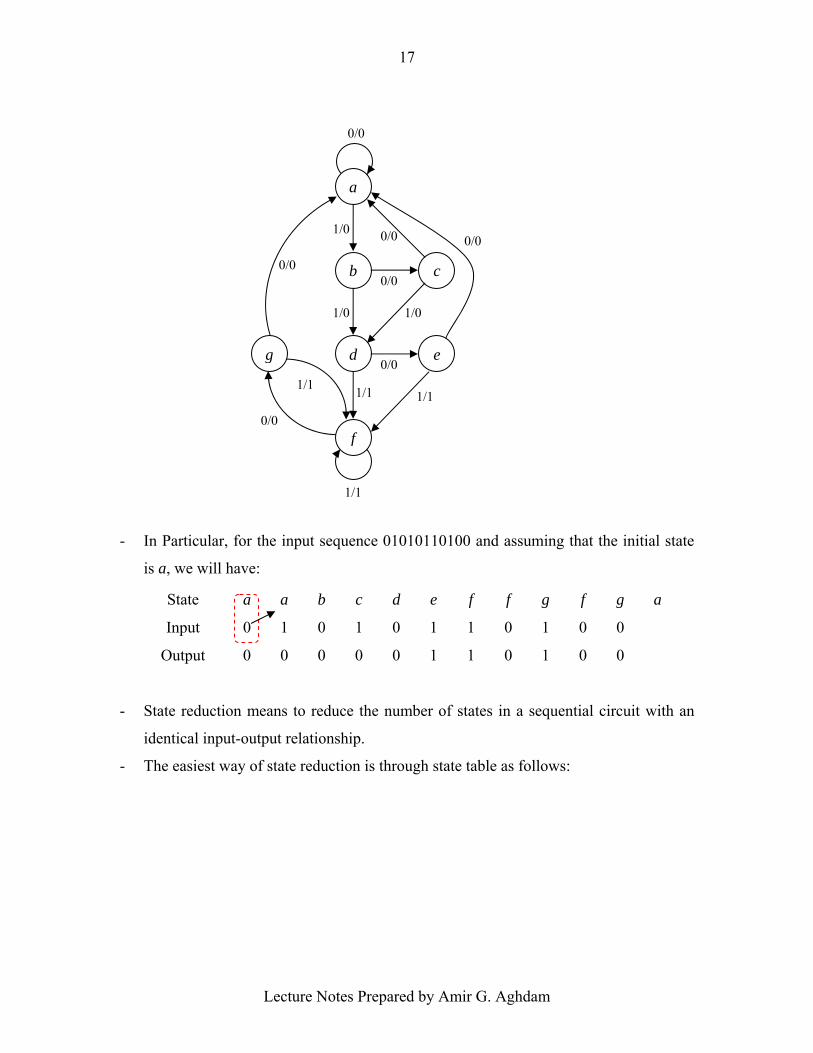
- In Particular, for the input sequence 01010110100 and assuming that the initial state
is a, we will have:
- State reduction means to reduce the number of states in a sequential circuit with an
identical input-output relationship.
- The easiest way of state reduction is through state table as follows:
State a a b c d e f f g f g a
Input 0 1 0 1 0 1 1 0 1 0 0
Output 0 0 0 0 0 1 1 0 1 0 0
a
c
1/1
0/0 b
e
1/1
0/0
1/0
0/0
0/0
d
f
g
1/0
0/0
1/0
1/1
0/0
1/1
0/0
Lecture Notes Prepared by Amir G. Aghdam
18
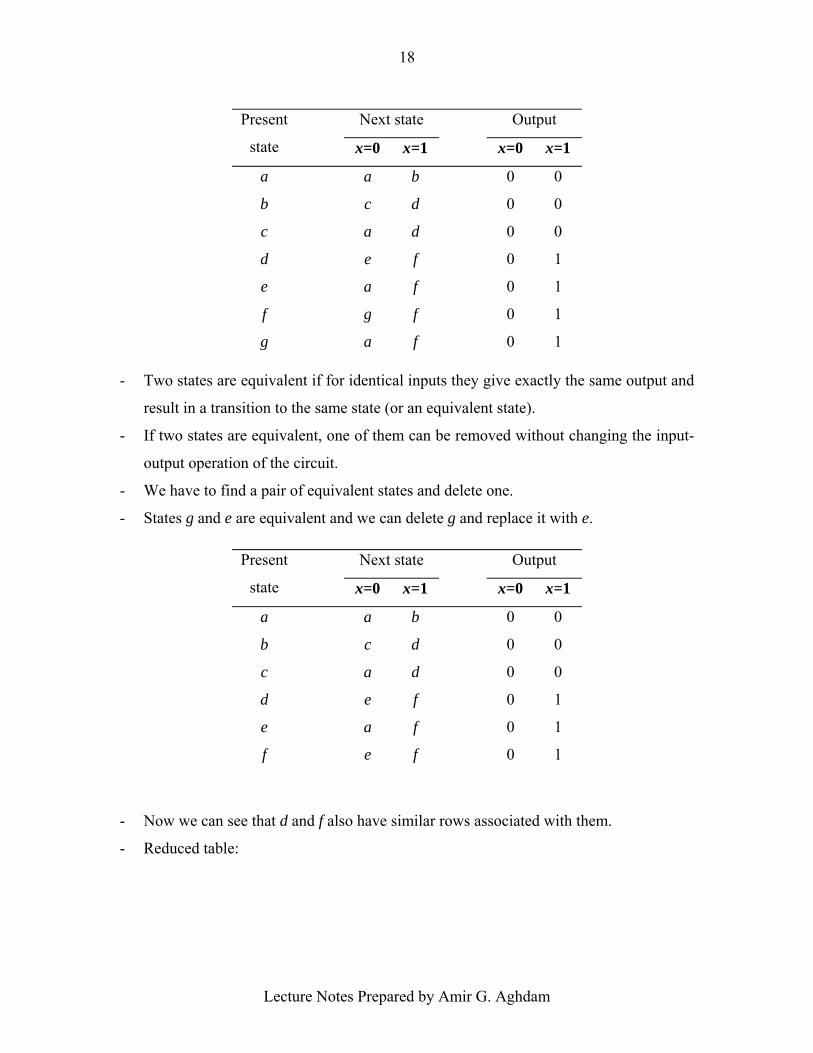
- Two states are equivalent if for identical inputs they give exactly the same output and
result in a transition to the same state (or an equivalent state).
- If two states are equivalent, one of them can be removed without changing the input-
output operation of the circuit.
- We have to find a pair of equivalent states and delete one.
- States g and e are equivalent and we can delete g and replace it with e.
- Now we can see that d and f also have similar rows associated with them.
- Reduced table:
Present
state
Next state Output
x=0 x=1 x=0 x=1
a a b 0 0
b c d 0 0
c a d 0 0
d e f 0 1
e a f 0 1
f g f 0 1
g a f 0 1
Present
state
Next state Output
x=0 x=1 x=0 x=1
a a b 0 0
b c d 0 0
c a d 0 0
d e f 0 1
e a f 0 1
f e f 0 1
Lecture Notes Prepared by Amir G. Aghdam
19
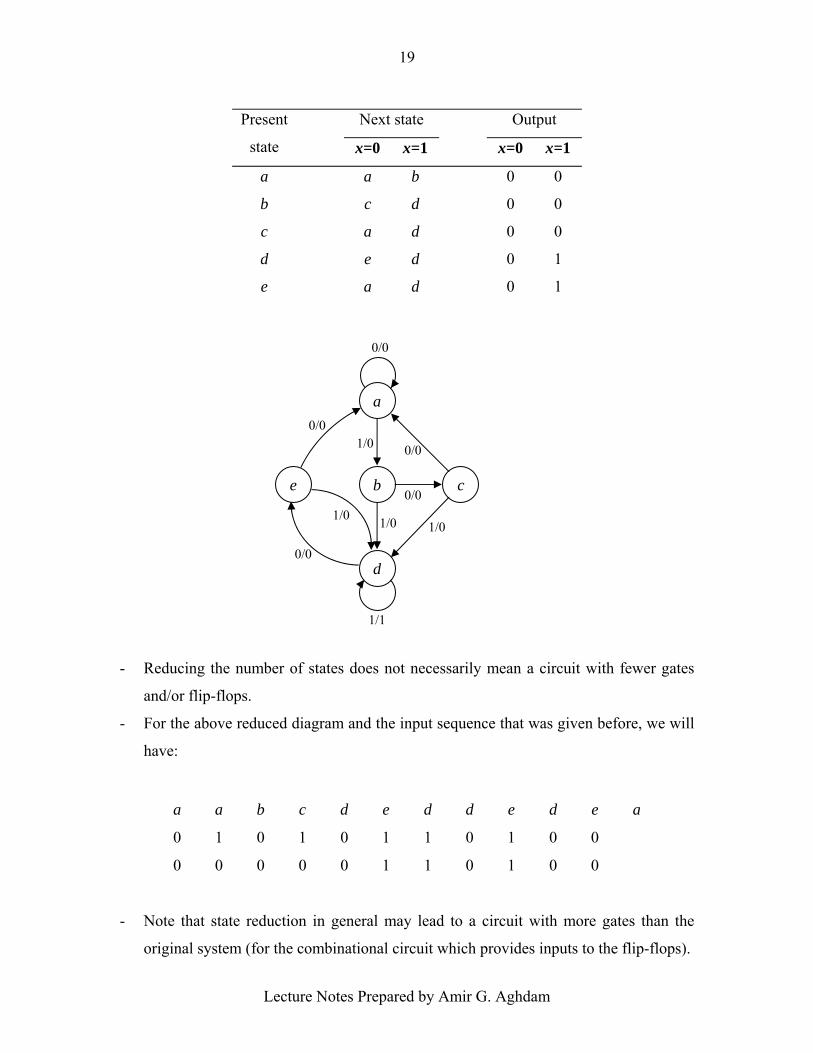
- Reducing the number of states does not necessarily mean a circuit with fewer gates
and/or flip-flops.
- For the above reduced diagram and the input sequence that was given before, we will
have:
- Note that state reduction in general may lead to a circuit with more gates than the
original system (for the combinational circuit which provides inputs to the flip-flops).
Present
state
Next state Output
x=0 x=1 x=0 x=1
a a b 0 0
b c d 0 0
c a d 0 0
d e d 0 1
e a d 0 1
a a b c d e d d e d e a
0 1 0 1 0 1 1 0 1 0 0
0 0 0 0 0 1 1 0 1 0 0
a
c
0/0
be
1/1
0/0
1/0
0/0
d
1/0
0/0
1/0
0/0
1/0
Lecture Notes Prepared by Amir G. Aghdam
20
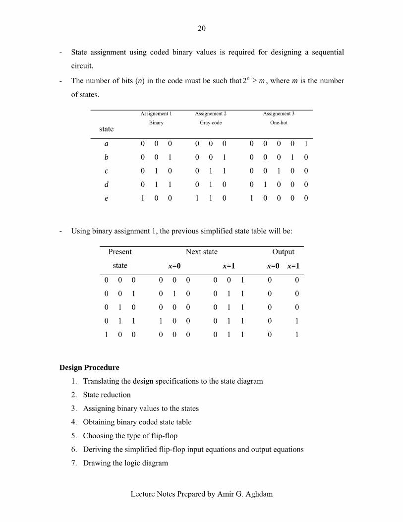
- State assignment using coded binary values is required for designing a sequential
circuit.
- The number of bits (n) in the code must be such that mn ≥2 , where m is the number
of states.
- Using binary assignment 1, the previous simplified state table will be:
Design Procedure
1. Translating the design specifications to the state diagram
2. State reduction
3. Assigning binary values to the states
4. Obtaining binary coded state table
5. Choosing the type of flip-flop
6. Deriving the simplified flip-flop input equations and output equations
7. Drawing the logic diagram
state
Assignement 1
Binary Assignement 2
Gray code Assignement 3
One-hot
a 0 0 0 0 0 0 0 0 0 0 1
b 0 0 1 0 0 1 0 0 0 1 0
c 0 1 0 0 1 1 0 0 1 0 0
d 0 1 1 0 1 0 0 1 0 0 0
e 1 0 0 1 1 0 1 0 0 0 0
Present
state
Next state Output
x=0 x=1 x=0 x=1
0 0 0 0 0 0 0 0 1 0 0
0 0 1 0 1 0 0 1 1 0 0
0 1 0 0 0 0 0 1 1 0 0
0 1 1 1 0 0 0 1 1 0 1
1 0 0 0 0 0 0 1 1 0 1
Lecture Notes Prepared by Amir G. Aghdam
21
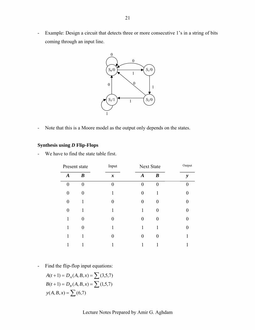
- Example: Design a circuit that detects three or more consecutive 1’s in a string of bits
coming through an input line.
- Note that this is a Moore model as the output only depends on the states.
Synthesis using D Flip-Flops
- We have to find the state table first.
- Find the flip-flop input equations:
∑∑∑
=
==+
==+
)7,6(),,(
)7,5,1(),,()1(
)7,5,3(),,()1(
xBAy
xBADtB
xBADtA
B
A
Present state Input Next State Output
A B x A B y
0 0 0 0 0 0
0 0 1 0 1 0
0 1 0 0 0 0
0 1 1 1 0 0
1 0 0 0 0 0
1 0 1 1 1 0
1 1 0 0 0 1
1 1 1 1 1 1
1
S0/0 S1/01
1
0
S3/1 S2/01
00
0

Lecture Notes Prepared by Amir G. Aghdam
22
- Simplify using K-map:
xBxADA .. +=
xBxADB .. ′+=
0
0
0
1
1
1
0
0
Bx A
A’
A
0
1
00 01 11 10
x’ x’ x
B’ B
0
0
1
1
0
1
0
0
Bx A
A’
A
0
1
00 01 11 10
x’ x’ x
B’ B
Lecture Notes Prepared by Amir G. Aghdam
23
BAy .=
- Design with other types of flip-flops is not straightforward as the next state cannot
directly be related to the input equations.
- In such cases we should use excitation tables, which list the required input for a given
change of state.
0
0
0
0
0
1
0
1
Bx A
A’
A
0
1
00 01 11 10
x’ x’ x
B’ B
D
CLK
x
A
D
C
C
B
B’
y
Lecture Notes Prepared by Amir G. Aghdam
24
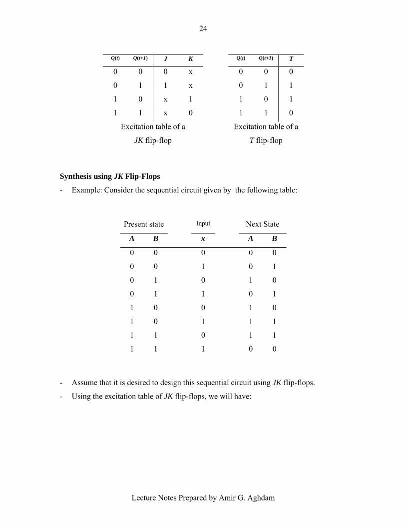
Synthesis using JK Flip-Flops
- Example: Consider the sequential circuit given by the following table:
- Assume that it is desired to design this sequential circuit using JK flip-flops.
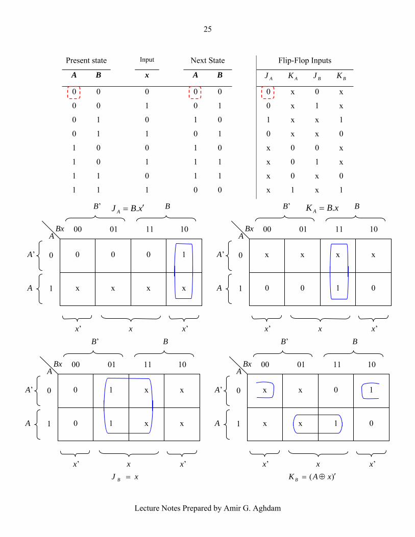
- Using the excitation table of JK flip-flops, we will have:
Q(t) Q(t+1) J K Q(t) Q(t+1) T
0 0 0 x 0 0 0
0 1 1 x 0 1 1
1 0 x 1 1 0 1
1 1 x 0 1 1 0
Excitation table of a
JK flip-flop
Excitation table of a
T flip-flop
Present state Input Next State
A B x A B
0 0 0 0 0
0 0 1 0 1
0 1 0 1 0
0 1 1 0 1
1 0 0 1 0
1 0 1 1 1
1 1 0 1 1
1 1 1 0 0
Lecture Notes Prepared by Amir G. Aghdam
25
xJ B = )( ′⊕= xAK B
Present state Input Next State Flip-Flop Inputs
A B x A B AJ AK BJ BK
0 0 0 0 0 0 x 0 x
0 0 1 0 1 0 x 1 x
0 1 0 1 0 1 x x 1
0 1 1 0 1 0 x x 0
1 0 0 1 0 x 0 0 x
1 0 1 1 1 x 0 1 x
1 1 0 1 1 x 0 x 0
1 1 1 0 0 x 1 x 1
0
x
0
x
0
x
1
x
Bx A
A’
A
0
1
00 01 11 10
x’ x’ x
B’ B
x
0
x
0
x
1
x
0
Bx A
A’
A
0
1
00 01 11 10
x’ x’ x
B’ B
0
0
1
1
x
x
x
x
Bx A
A’
A
0
1
00 01 11 10
x’ x’ x
B’ B
x
x
x
x
0
1
1
0
Bx A
A’
A
0
1
00 01 11 10
x’ x’ x
B’ B
xBJ A ′= . xBK A .=
Lecture Notes Prepared by Amir G. Aghdam
26
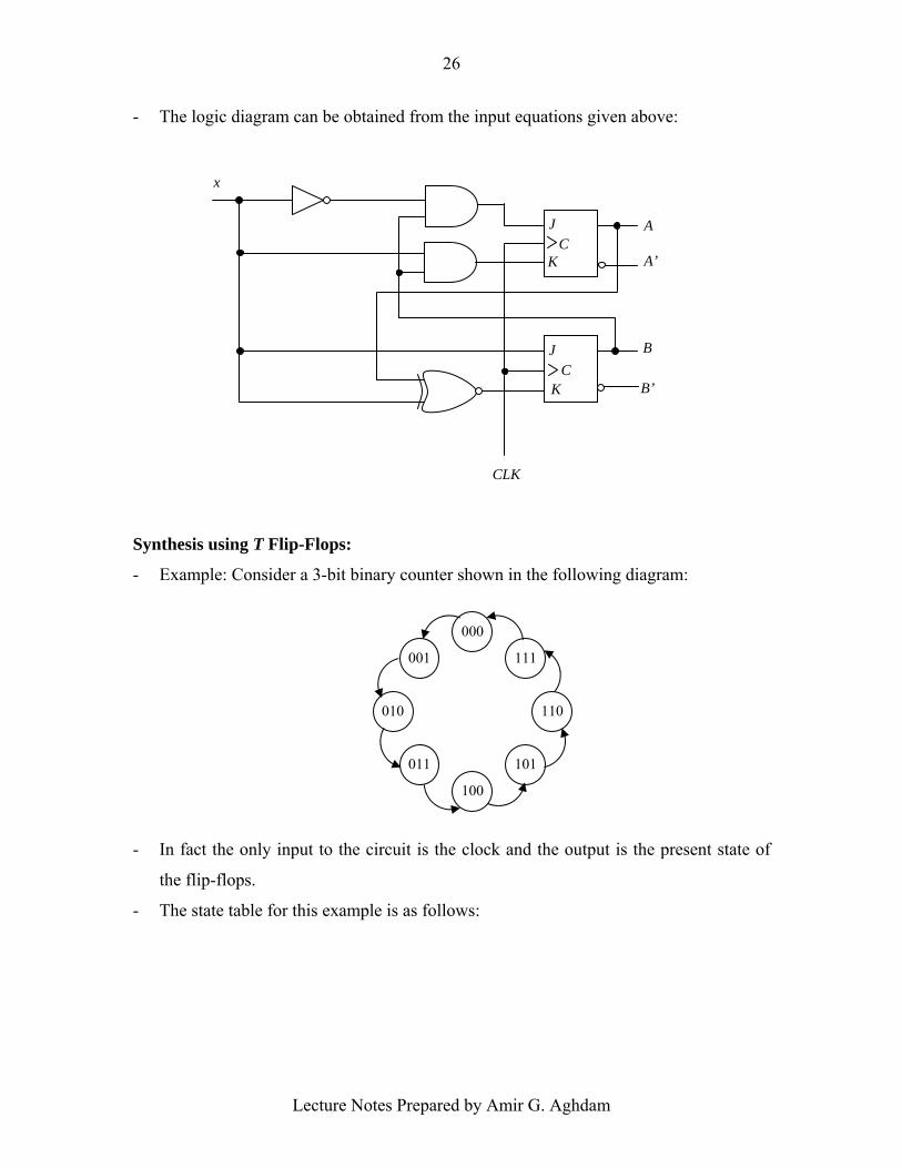
- The logic diagram can be obtained from the input equations given above:
Synthesis using T Flip-Flops:
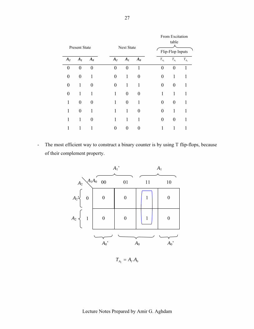
- Example: Consider a 3-bit binary counter shown in the following diagram:
- In fact the only input to the circuit is the clock and the output is the present state of
the flip-flops.
- The state table for this example is as follows:
000
001
010
111
110
101
100
011
J
CLK
x
A
J
K
K
B C
CA’
B’
Lecture Notes Prepared by Amir G. Aghdam
27
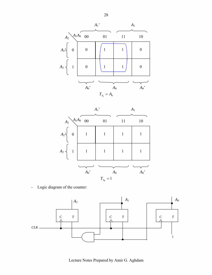
- The most efficient way to construct a binary counter is by using T flip-flops, because
of their complement property.
01.2AATA =
From Excitation table
Present State Next State Flip-Flop Inputs
A2 A1 A0 A2 A1 A0 2AT
1AT0AT
0 0 0 0 0 1 0 0 1
0 0 1 0 1 0 0 1 1
0 1 0 0 1 1 0 0 1
0 1 1 1 0 0 1 1 1
1 0 0 1 0 1 0 0 1
1 0 1 1 1 0 0 1 1
1 1 0 1 1 1 0 0 1
1 1 1 0 0 0 1 1 1
0
0
0
0
1
1
0
0
A1A0 A2
A2’
A2
0
1
00 01 11 10
A0’ A0’ A0
A1’ A1
Lecture Notes Prepared by Amir G. Aghdam
28
01ATA =
10=AT
- Logic diagram of the counter:
0
0
1
1
1
1
0
0
A1A0 A2
A2’
A2
0
1
00 01 11 10
A0’ A0’ A0
A1’ A1
1
1
1
1
1
1
1
1
A1A0 A2
A2’
A2
0
1
00 01 11 10
A0’ A0’ A0
A1’ A1
CLK
A2
C T C T C T
1
A1 A0

Lecture Notes Prepared by Amir G. Aghdam
29
Reference:
[1] Digital Design 3rd Edition, By Morris Mano, Publisher Prentice Hall, 4th Edition.