Embed Size (px)
Citation preview

Lecture Notes Prepared by Amir G. Aghdam
1
COEN 312 DIGITAL SYSTEMS DESIGN - LECTURE NOTES
Concordia University
Chapter 4: Combinational Logic
NOTE: For more examples and detailed description of the material in the lecture notes, please refer to the main textbook: Digital Design 3rd Edition, By Morris Mano, Publisher Prentice Hall, 4th Edition All examples used in the lecture notes are from the above reference. Combinational Circuits
- A combinational circuit consists of input variables, output variables, and logic gates
that transform binary information from the input to the output.
- A combinational circuit cannot have any storage elements (registers) or any feedback
paths (connections from the output of one gate to the input of a second gate that
directly or indirectly affects the input to the first gate).
- As an example, consider the following combinational circuit with 3 inputs and 2
outputs (n = 3, m = 2):
Combinational
circuit n inputs m outputs
F’2
A B C A B C
A B
A C
B C
T1
T2
T3
F2
F1

Lecture Notes Prepared by Amir G. Aghdam
2
- If there are more than two levels of gates to generate a function, label the output of
the corresponding gates and determine the Boolean expression for each of them (here,
we have used the labels T1, T2, T3, and F’2 to find the Boolean expression for F1).
231
123
2
1
2
.'..
...
TTFTFTCBAT
CBATCBCABAF
+===
++=++=
- By using the properties of Boolean algebra, the expression for 1F will be equal to:
CBACBACBACBAF ..''..'.'.'.'.1 +++=
- The truth table for the outputs of this combinational circuit can be obtained by using
the above expressions for 1F and 2F , or by using the labeled gate outputs in the truth
table and obtaining 231 TTF += and CBCABAF ...2 ++= for different combinations
of the input variables as follows:
A B C F2 F’2 T1 T2 T3 F1
0
0
0
0
1
1
1
1
0
0
1
1
0
0
1
1
0
1
0
1
0
1
0
1
0
0
0
1
0
1
1
1
1
1
1
0
1
0
0
0
0
1
1
1
1
1
1
1
0
0
0
0
0
0
0
1
0
1
1
0
1
0
0
0
0
1
1
0
1
0
0
1

Lecture Notes Prepared by Amir G. Aghdam
3
- This is in fact the logic circuit for a full adder ( [ ][ ]12 FFCBA =++ ).
Design Procedure
- Important design constraints include the number of gates, number of inputs to a gate,
propagation time of the signal through the gates, number of interconnections, etc.
Example
- Find a combinational circuit, which converts the binary coded decimal (BCD) to the
excess-3 code for the decimal digits.
Input BCD Output Excess-3 Code
A B C D w x y z
0 0 0 0 0 0 1 1
0 0 0 1 0 1 0 0
0
0
0
0
0
0
1
1
0
0
1
1
1
1
0
0
1
1
0
0
1
1
0
0
0
1
0
1
0
1
0
1
0
0
0
1
1
1
1
1
1
1
1
0
0
0
0
1
0
1
1
0
0
1
1
0
1
0
1
0
1
0
1
0

Lecture Notes Prepared by Amir G. Aghdam
4
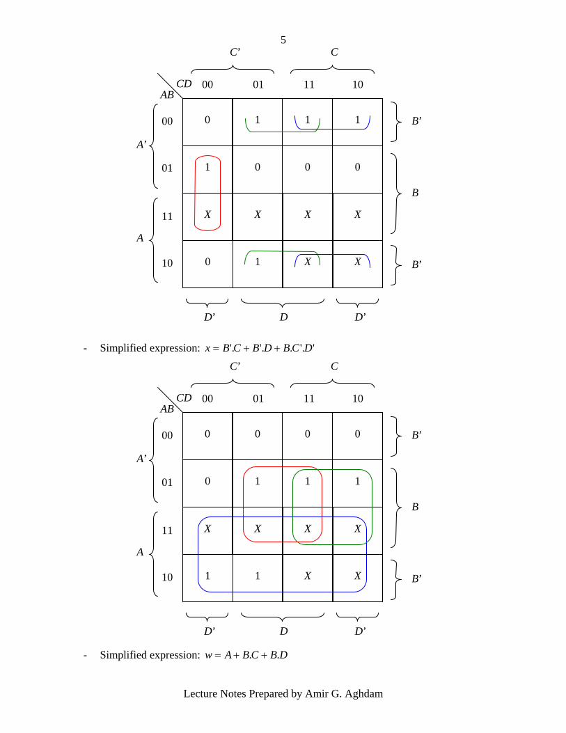
- Simplified expression: 'Dz =
- Simplified expression: ''.. DCDCy +=
X
0
X
0
0
1
1
0
1
1
CD AB
00
01
00 01 11 10
D’ D’ D
C’ C
X
1
0
X
X
X
11
10
B’
B’
B
A’
A
X
1
X
0
1
1
1
0
0
0
CD AB
00
01
00 01 11 10
D’ D’ D
C’ C
X
1
0
X
X
X
11
10
B’
B’
B
A’
A
Lecture Notes Prepared by Amir G. Aghdam
5
- Simplified expression: ''..'.'. DCBDBCBx ++=
- Simplified expression: DBCBAw .. ++=
X
0
X
0
1
0
1
1
1
0
CD AB
00
01
00 01 11 10
D’ D’ D
C’ C
X
0
1
X
X
X
11
10
B’
B’
B
A’
A
0
X
1
X
1
0
0
0
0
1
CD AB
00
01
00 01 11 10
D’ D’ D
C’ C
X
1
1
X
X
X
11
10
B’
B’
B
A’
A

Lecture Notes Prepared by Amir G. Aghdam
6
- Using the above simplified expressions in sum of products, one can implement this
combinational circuit using seven AND gates and three OR gates.
- One can use the properties of Boolean algebra to change the expressions in a way that
some of the terms are shared between the output functions to make the
implementation even simpler (fewer gates) as follows:
).(..
)'.()'.(''..)'.(''..'.'.
)'(.''..
'
DCBADBCBAw
DCBDCBDCBDCBDCBDBCBx
DCDCDCDCy
Dz
++=++=
+++=++=++=
++=+=
=
- These expressions can be implemented using four AND gates and four OR gates and
one inverter (we assume that the inputs are available in both normal and complement
forms).
C+D
x
y
w
z
A
B
C D

Lecture Notes Prepared by Amir G. Aghdam
7
Binary Adder-Subtractor
- A combinational circuit that implements the addition of two bits is referred to as a
half adder.
- A combinational circuit that implements the addition of three bits (two significant bits
and a previous carry) is referred to as a full adder.
- A full adder can be implemented by using two half adders.
- Assuming that S and C denote the sum (the lower significant bit in the binary sum)
and the carry (the higher significant bit in the binary sum) of the two input variables
of a half adder, we will have:
yxCyx
yxyxS
.
'.'.
=⊕=+=
x y C S
0 0 0 0
0 1 0 1
1 0 0 1
1 1 1 0
S
C
x y’
x’ y
x y
x y S
C

Lecture Notes Prepared by Amir G. Aghdam
8
- For a full adder, where the third input z denotes the carry corresponding to the
addition of the previous lower significant bits, we have:
- Simplified expression: zyxzyxzyxzyxS ..''..'.'.'.'. +++= or: zyxS ⊕⊕=
x y z C S
0
0
0
0
1
1
1
1
0
0
1
1
0
0
1
1
0
1
0
1
0
1
0
1
0
0
0
1
0
1
1
1
0
1
1
0
1
0
0
1
0
1
1
0
0
1
1
0
yz x
x’
x
0
1
00 01 11 10
z’ z’ z
y’ y

Lecture Notes Prepared by Amir G. Aghdam
9
- Simplified expression: zyzxyxC ... ++= or zyxyxzyxzyxyxC ).(..'.'... ⊕+=++=
- We will have the following logic circuits:
- Using the second expression given for S and C, we can implement the full adder with
two half adders and an OR gate as shown below:
0
0
0
1
1
1
0
1
yz x
x’
x
0
1
00 01 11 10
z’ z’ z
y’ y
x’ y’ z x’ y z’ x y’ z’ x y z
S
x y
x z
y z
C
x y
z
C
S
Lecture Notes Prepared by Amir G. Aghdam
10
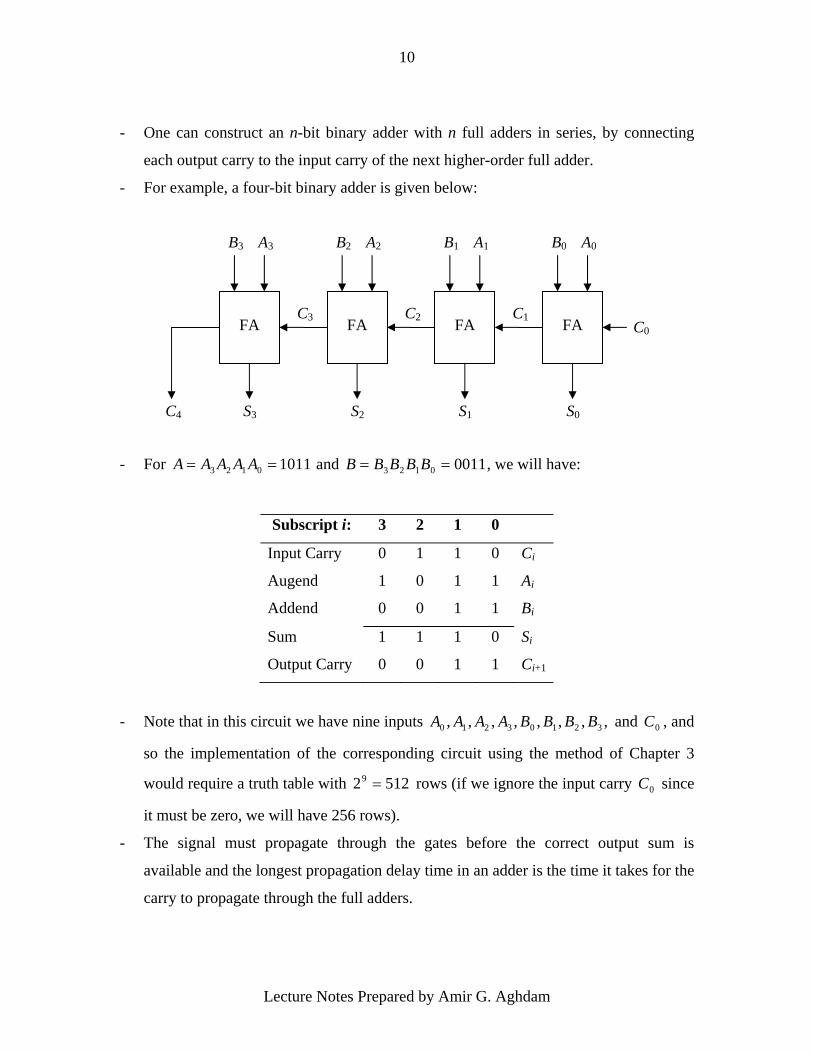
- One can construct an n-bit binary adder with n full adders in series, by connecting
each output carry to the input carry of the next higher-order full adder.
- For example, a four-bit binary adder is given below:
- For 10110123 == AAAAA and 00110123 == BBBBB , we will have:
Subscript i: 3 2 1 0
Input Carry 0 1 1 0 Ci
Augend 1 0 1 1 Ai
Addend 0 0 1 1 Bi
Sum 1 1 1 0 Si
Output Carry 0 0 1 1 Ci+1
- Note that in this circuit we have nine inputs ,,,,,,,, 32103210 BBBBAAAA and 0C , and
so the implementation of the corresponding circuit using the method of Chapter 3
would require a truth table with 51229 = rows (if we ignore the input carry 0C since
it must be zero, we will have 256 rows).
- The signal must propagate through the gates before the correct output sum is
available and the longest propagation delay time in an adder is the time it takes for the
carry to propagate through the full adders.
FA
S3
A3 B3
C0
C4
FA
S2
A2 B2
C3
FA
S1
A1 B1
C2
FA
S0
A0 B0
C1

Lecture Notes Prepared by Amir G. Aghdam
11
Ai
Bi
Ci
Ci+1
Si
Pi
Gi
- The output of each full adder will not settle to its final value until the input carry is
available from the previous stage.
- For a full adder, the carry propagates through an AND gate and an OR gate which
constitutes two gate levels, which implies that in an n-bit adder, the carry propagates
from input to output through 2n gate levels.
- Use faster gates with reduced delays.
- Reduce the carry delay time by increasing the equipment complexity properly.
- One of the popular methods for this purpose is to use carry lookahead as follows:
iii
iii
BAGBAP
.=⊕=
- iP and iG are referred to as carry propagate and carry generate respectively.
- The output sum and carry can then be written as:
iiii
iii
CPGCCPS
.1 +=⊕=
+
- We now use iterations to obtain each output carry 1+iC directly from the input carry
0C as follows:

Lecture Notes Prepared by Amir G. Aghdam
12
001230123123233
0012012122333334
0012012122001011222223
001011000111112
0001
..........).......(.
......)....(....)..(.
.
CPPPPGPPPGPPGPGCPPPGPPGPGPGCPGC
CPPPGPPGPGCPPGPGPGCPGCCPPGPGCPGPGCPGC
CPGC
++++=++++=+=
+++=+++=+=++=++=+=
+=
- Since all these expressions are in standard form, one can use a two-level circuit to
implement this combinational system.
- A 4-bit adder with a carry lookahead scheme is given below:
B3
A3 P3
G3
B0
A0 P0
G0
B2
A2 P2
G2
B1
A1
G1
P1
C0 C0
Carry Lookahead Generator
P0
P1 S1
P2
S0
S2
S3
C4 C4
C3
C2
C1
P3

Lecture Notes Prepared by Amir G. Aghdam
13
- Binary subtraction BA − can be done by adding A to the 2’s complement of B
(which can be obtained by adding one to the 1’s complement).
- The logic circuit for a 4-bit adder/subtractor is given as follows:
- The mode input M controls the output.
- When M is 0, then BB =⊕ 0 and the input carry is 0 which means that the output of
the circuit is equal to A plus B .
- When M is 1, we have '1 BB =⊕ and the input carry is 1, which implies that the
output is equal to A plus the 1’s complement of B plus 1. This means that the output
is A minus B (provided there is no overflow).
- Addition of two n-bit numbers which are both positive or both negative, may result in
an overflow, i.e., the result may exceed the capacity of an n-bit register. This is shown
for 8-bit registers below:
Carries: 0 1
+70 0 1000110
+80 0 1010000
+150 1 0010110
FA
S3
A3 B3
C0
FA
S0
A0 B0
C1
FA
S1
A1 B1
C2
FA
S2
A2 B2
C3
C4
M

Lecture Notes Prepared by Amir G. Aghdam
14
- In general, an overflow can be detected by applying exclusive-OR operation on the
input carry and output carry of the sign bit position (the leftmost digit).
- Note that if the last two carries were equal, there would be no overflow.
- For example, for the 4-bit adder subtractor, we will have:
- If the numbers are unsigned (the numbers are considered positive and the leftmost bit
does not represent the sign), the circuit performs A minus B if BA ≥ or the 2’s
complement of B minus A if BA ≤ .
- For two unsigned numbers, the output carry of the leftmost bits detects a carry after
addition or a borrow after subtraction.
Carry: 1
70 1000110
80 1010000
150 0010110
Decimal Adder
- The most common way to code a decimal number is binary coded decimal (BCD),
where the decimal number is represented by encoding each digit in binary form.
- Applying two BCD digits to a 4-bit binary adder will result in a number ranging from
0 to 9+9+1=19 as shown in the following table:
Carries: 1 0
-70 1 0111010
-80 1 0110000
-150 0 1101010
C4
C3 V

Lecture Notes Prepared by Amir G. Aghdam
15
Binary Sum BCD Sum Decimal
K Z8 Z4 Z2 Z1 C S8 S4 S2 S1
0 0 0 0 0 0 0 0 0 0 0
0 0 0 0 1 0 0 0 0 1 1
0 0 0 1 0 0 0 0 1 0 2
0 0 0 1 1 0 0 0 1 1 3
0 0 1 0 0 0 0 1 0 0 4
0 0 1 0 1 0 0 1 0 1 5
0 0 1 1 0 0 0 1 1 0 6
0 0 1 1 1 0 0 1 1 1 7
0 1 0 0 0 0 1 0 0 0 8
0 1 0 0 1 0 1 0 0 1 9
0 1 0 1 0 1 0 0 0 0 10
0 1 0 1 1 1 0 0 0 1 11
0 1 1 0 0 1 0 0 1 0 12
0 1 1 0 1 1 0 0 1 1 13
0 1 1 1 0 1 0 1 0 0 14
0 1 1 1 1 1 0 1 0 1 15
1 0 0 0 0 1 0 1 1 0 16
1 0 0 0 1 1 0 1 1 1 17
1 0 0 1 0 1 1 0 0 0 18
1 0 0 1 1 1 1 0 0 1 19
- The left side of the table gives the output of a 4-bit binary adder but we want the
output to be in a BCD form.
- From the entries of the table, it can be concluded that a conversion from binary sum
to BCD representation is needed if K=1 or Z8 and Z4 are both equal to 1 or Z8 and Z2
are both equal to 1.
- The Boolean expression to show the condition for a correction is:
Lecture Notes Prepared by Amir G. Aghdam
16
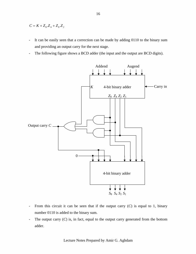
2848 .. ZZZZKC ++=
- It can be easily seen that a correction can be made by adding 0110 to the binary sum
and providing an output carry for the next stage.
- The following figure shows a BCD adder (the input and the output are BCD digits).
- From this circuit it can be seen that if the output carry (C) is equal to 1, binary
number 0110 is added to the binary sum.
- The output carry (C) is, in fact, equal to the output carry generated from the bottom
adder.
Output carry C
S8 S4 S2 S1
K 4-bit binary adder
Z8 Z4 Z2 Z1
Addend Augend
4-bit binary adder
Carry in
0

Lecture Notes Prepared by Amir G. Aghdam
17
Binary Multiplier
- Multiplication of binary numbers is similar to the multiplication of decimal numbers
as shown below for a 2-bit binary number:
B1 B0
A1 A0
A0. B1 A0. B0
A1. B1 A1. B0
C3 C2 C1 C0
- So, multiplication of two 2-bit numbers can be implemented by a combinational
circuit with two half adders as follows:
- Assume now that the multiplier has 3 bits and the multiplicand has 4 bits.
B1
B1
HA
HA
A0
A1 B0
B0
C0 C1 C2 C3

Lecture Notes Prepared by Amir G. Aghdam
18
B3 B2 B1 B0
A2 A1 A0
A0. B3 A0. B2 A0. B1 A0. B0
A1. B3 A1. B2 A1. B1 A1. B0
A2. B3 A2. B2 A2. B1 A2. B0
C6 C5 C4 C3 C2 C1 C0
- In this case, we will need two 4-bit adders and 12 AND gates as follows:
A1 B0 B1 B2 B3
A2 B0 B1 B2 B3
Addend Augend 4-bit adder
Sum and output carry
Addend Augend 4-bit adder
Sum and output carry
A0 B0 B1 B2 B3
0
C0 C1 C2 C3 C4 C5 C6

Lecture Notes Prepared by Amir G. Aghdam
19
- In general, if the multiplier has J bits and the multiplicand has K bits, we will need
1−J K-bit adders and KJ × AND gates and the product will have KJ + bits.
Magnitude Comparator
- A magnitude comparator is a combinational circuit that compares two numbers A and
B and determines whether A > B, A = B, or A < B.
- Comparison operation should start by comparing the most significant bits of A and B.
- For example, consider two numbers A and B as follows:
0123
0123
BBBBBAAAAA
==
- Define the following functions (which are the bib-by-bit exclusive-NOR operations
on A and B):
3,2,1,0 for''.. =+= iBABAx iiiii
- It can easily be verified that:
1..........
1..........
1...
0'01231
'1232
'233
'3
'00123
'1123
'223
'33
0123
=+++⇒<
=+++⇒>
=⇒=
BAxxxBAxxBAxBABA
BAxxxBAxxBAxBABA
xxxxBA
- In the equations for inequalities, the most significant bits (with the same significance)
in the two numbers are compared and if one of them is 1 and the other one is 0, the
comparison is finished and only if they are equal, the next significant bits in the two
numbers will be compared (this is represented by ANDing the ix ’s with
corresponding terms in the inequalities).
- A 4-bit magnitude comparator logic circuit is given below:

Lecture Notes Prepared by Amir G. Aghdam
20
Decoders
- Decoder circuits are used to decode encoded information.
- A decoder is a combinational circuit that has n inputs and a maximum of n2 outputs.
- The truth table for a 3-to-8-line decoder is as follows:
(A=B)
(A>B)
(A<B)
x2
A2
B2
x3
A3
B3
x1
A1
B1
x0
A0
B0

Lecture Notes Prepared by Amir G. Aghdam
21
- The logic circuit for this decoder is shown in the following figure, where each output
represents one of the minterms.
Inputs Outputs
x y z D0 D1 D2 D3 D4 D5 D6 D7
0 0 0 1 0 0 0 0 0 0 0
0 0 1 0 1 0 0 0 0 0 0
0 1 0 0 0 1 0 0 0 0 0
0 1 1 0 0 0 1 0 0 0 0
1 0 0 0 0 0 0 1 0 0 0
1 0 1 0 0 0 0 0 1 0 0
1 1 0 0 0 0 0 0 0 1 0
1 1 1 0 0 0 0 0 0 0 1
x
y
z
D0 = x’.y’.z’
D1 = x’.y’.z
D2 = x’.y.z’
D3 = x’.y.z
D4 = x.y’.z’
D5 = x.y’.z
D6 = x.y.z’
D7 = x.y.z
3×8 Decoder

Lecture Notes Prepared by Amir G. Aghdam
22
- Sometimes NAND gates are used instead of AND gates to generate complemented
outputs.
- One or more enable inputs are often used in the decoders to control the operation of
the circuit.
- A 2-to-4-line decoder consisting of NAND gates with an enable input is given below:
- The corresponding truth table is as follows:
- In general, the enable input signal E may be activated with a 0 or with a 1.
- Some decoders have more than one enable input, which must be equal to a specific
binary number in order to enable the circuit.
E A B D0 D1 D2 D3
1 X X 1 1 1 1
0 0 0 0 1 1 1
0 0 1 1 0 1 1
0 1 0 1 1 0 1
0 1 1 1 1 1 0
A’ B’
A’ B
A B’
A B
E
D0
D1
D2
D3

Lecture Notes Prepared by Amir G. Aghdam
23
- A demultiplexer is a circuit that receives data from a single input line and directs it to
one of the output lines, which is determined by selection lines.
- One can build a demultiplexer by using a decoder with an enable line, as can be seen
in the above example.
- In the above example, E is the data input line and A and B are selection inputs which
determine which output will be the same as the input value E (this can easily be seen
from the circuit).
- One can connect multiple decoders with enable lines to build a decoder with a greater
number of outputs.
- For example, two 3-to-8-line decoders with enable lines can be connected to construct
a 4-to-16-line decoder as follows:
- The minterms 0000 to 0111 are generated by the top decoder, while the bottom one
generates minterms 1000 to 1111 as shown below:
D8 to D15
D0 to D7 3×8
Decoder
E
3×8 Decoder
E
x y z
w

Lecture Notes Prepared by Amir G. Aghdam
24
- In the first table D8 to D15 are all zero and D0 to D7 in the second one are all zero
(assuming that the decoder is constructed by AND gates not NAND gates).
- In general, in logic components, enable inputs are used for interconnecting two or
more components.
Inputs Outputs
w x y z D0 D1 D2 D3 D4 D5 D6 D7
0 0 0 0 1 0 0 0 0 0 0 0
0 0 0 1 0 1 0 0 0 0 0 0
0 0 1 0 0 0 1 0 0 0 0 0
0 0 1 1 0 0 0 1 0 0 0 0
0 1 0 0 0 0 0 0 1 0 0 0
0 1 0 1 0 0 0 0 0 1 0 0
0 1 1 0 0 0 0 0 0 0 1 0
0 1 1 1 0 0 0 0 0 0 0 1
Inputs Outputs
w x y z D8 D9 D10 D11 D12 D13 D14 D15
1 0 0 0 1 0 0 0 0 0 0 0
1 0 0 1 0 1 0 0 0 0 0 0
1 0 1 0 0 0 1 0 0 0 0 0
1 0 1 1 0 0 0 1 0 0 0 0
1 1 0 0 0 0 0 0 1 0 0 0
1 1 0 1 0 0 0 0 0 1 0 0
1 1 1 0 0 0 0 0 0 0 1 0
1 1 1 1 0 0 0 0 0 0 0 1

Lecture Notes Prepared by Amir G. Aghdam
25
- Any n-input m-output combinational logic circuit can be implemented by using an n-
to-2n-line decoder (to generate different minterms) and m OR gates (to generate sum
of products).
- For example, a full adder can be implemented as follows:
∑∑
=
=
)7,6,5,3(),,(
)7,4,2,1(),,(
zyxC
zyxS
- If the number of minterms in the Boolean expression of a function is more than half
of the number of the outputs of the decoder, it is easier to implement the complement
function and then use a NOR gate instead of an OR gate, which will result in the same
function with smaller number of inputs for the gate.
- If the decoder is implemented by NAND gates, one can use bubble technique and
implement the function with a NAND gate instead of an OR gate in the output of the
decoder.
Encoders
- An encoder’s operation is the inverse operation of a decoder.
- For example, an octal-to-binary encoder is given below:
3×8 Decoder
01234567
22
21
20
x
y
z C
S
Lecture Notes Prepared by Amir G. Aghdam
26
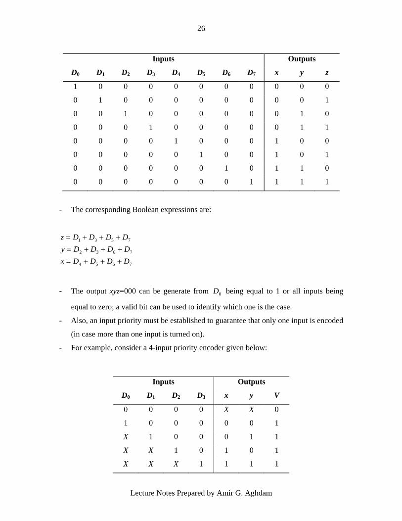
- The corresponding Boolean expressions are:
7654
7632
7531
DDDDxDDDDyDDDDz
+++=+++=+++=
- The output xyz=000 can be generate from 0D being equal to 1 or all inputs being
equal to zero; a valid bit can be used to identify which one is the case.
- Also, an input priority must be established to guarantee that only one input is encoded
(in case more than one input is turned on).
- For example, consider a 4-input priority encoder given below:
Inputs Outputs
D0 D1 D2 D3 D4 D5 D6 D7 x y z
1 0 0 0 0 0 0 0 0 0 0
0 1 0 0 0 0 0 0 0 0 1
0 0 1 0 0 0 0 0 0 1 0
0 0 0 1 0 0 0 0 0 1 1
0 0 0 0 1 0 0 0 1 0 0
0 0 0 0 0 1 0 0 1 0 1
0 0 0 0 0 0 1 0 1 1 0
0 0 0 0 0 0 0 1 1 1 1
Inputs Outputs
D0 D1 D2 D3 x y V
0 0 0 0 X X 0
1 0 0 0 0 0 1
X 1 0 0 0 1 1
X X 1 0 1 0 1
X X X 1 1 1 1
Lecture Notes Prepared by Amir G. Aghdam
27
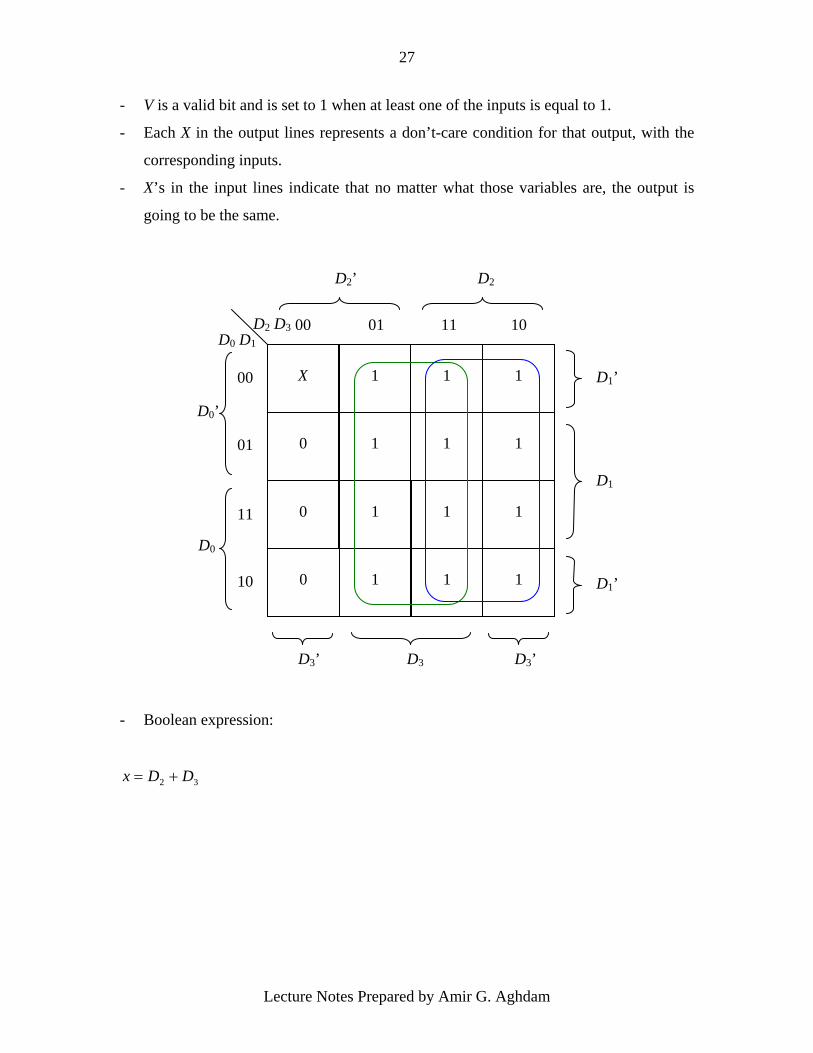
- V is a valid bit and is set to 1 when at least one of the inputs is equal to 1.
- Each X in the output lines represents a don’t-care condition for that output, with the
corresponding inputs.
- X’s in the input lines indicate that no matter what those variables are, the output is
going to be the same.
- Boolean expression:
32 DDx +=
1
1
1
1
1
X
0
1
1
1
D2 D3 D0 D1
00
01
00 01 11 10
D3’ D3’ D3
D2’ D2
0
0
1
1
1
1
11
10
D1’
D1’
D1
D0’
D0

Lecture Notes Prepared by Amir G. Aghdam
28
- Boolean expression:
'. 213 DDDy +=
- The valid bit V is simply equal to:
3210 DDDDV +++=
- The logic circuit of the above 4-input priority encoder is given below:
1
1
1
1
1
X
1
1
0
0
D2 D3 D0 D1
00
01
00 01 11 10
D3’ D3’ D3
D2’ D2
1
0
1
1
0
0
11
10
D1’
D1’
D1
D0’
D0

Lecture Notes Prepared by Amir G. Aghdam
29
Multiplexers
- A multiplexer or data selector is a combinational circuit that chooses one of the inputs
and reproduces the signal on this input at the output terminal.
- A 2-to-1-line multiplexer circuit and its block diagram are shown below:
- I0 and I1 are the input lines, S is the selection line, and Y is the output.
- A 2n-to-1-line Multiplexer is in fact a combination of a decoder, 2n AND gates, and
one OR gate.
- For example, a 4-to-1-line multiplexer can be built as follows:
y
x
V
D3
D2
D0
D1
MUX
1
0 I0 Y
I1
S
I0
I1
Y
S

Lecture Notes Prepared by Amir G. Aghdam
30
- One can combine the two-input AND gates with the two-input AND gates in the
decoder and use three-input AND gates instead, as follows:
S1 S0 Y
0 0 I0
0 1 I1
1 0 I2
1 1 I3
I0
I2
I1
I3
S1
S0
Y
2×4 Decoder
0 1 2
3
20
21
S0
S1
Y
I0
I1
I2
I3

Lecture Notes Prepared by Amir G. Aghdam
31
- The AND gates in fact decode the selection lines S0 to Sn-1 and the multiplexer is a
decoder with n2 additional lines (I0 to I2n
-1 ), each of which goes to one of the AND
gates.
- A multiplexer can have an enable line too.
- Multiplexer circuits can be combined to provide multiple bit selection logic.
- A circuit that selects one of two 4-bit sets of data lines can be provided by using 4 2-
to-1-line multiplexers as shown below:
E S Y3Y2Y1Y0
1 X All Zeros
0 0 A3A2A1A0
0 1 B3B2B1B0
A0
A1
A2
A3
B0
B1
B2
B3
S
E
Y0
Y1
Y2
Y3
(Enable)
(Select)

Lecture Notes Prepared by Amir G. Aghdam
32
- It can easily be verified that if S=0, the output lines Y0Y1Y2Y3 will be equal to
A0A1A2A3, provided the enable line is active (here E=0).
- If S=1, then the output lines Y0Y1Y2Y3 will be equal to B0B1B2B3, provided the enable
line is active (here E=0).
- The output lines are all 0’s when E=1.
- Since a multiplexer is in fact a decoder with an internal OR gate, one can use a
multiplexer to implement any Boolean function, in a way similar to the method that
was used to implement Boolean functions using a decoder and OR gates.
- For this purpose, the first n-1 variables will be used as selection inputs and the
remaining variable together with its complement, 1, and 0 will be used to build data
inputs.
- Look at each pair of rows (2n-1 pair of rows) in the truth table and try to see if the
corresponding function values are equal to 0, 1, the last variable in the input columns,
or its complement.
- For example, consider the following Boolean function:
∑= )7,6,2,1(),,( zyxF
- This function can be implemented as follows:
x y z F
0 0 0 0
0 0 1 1
0 1 0 1
0 1 1 0
1 0 0 0
1 0 1 0
1 1 0 1
1 1 1 1
F = z
F = z’
F = 0
F = 1
Lecture Notes Prepared by Amir G. Aghdam
33
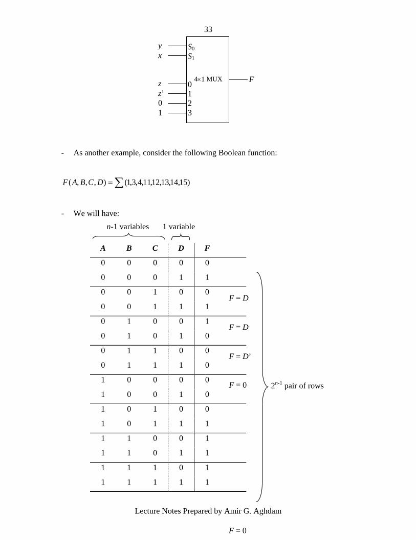
- As another example, consider the following Boolean function:
∑= )15,14,13,12,11,4,3,1(),,,( DCBAF
- We will have:
A B C D F
0 0 0 0 0
0 0 0 1 1
0 0 1 0 0
0 0 1 1 1
0 1 0 0 1
0 1 0 1 0
0 1 1 0 0
0 1 1 1 0
1 0 0 0 0
1 0 0 1 0
1 0 1 0 0
1 0 1 1 1
1 1 0 0 1
1 1 0 1 1
1 1 1 0 1
1 1 1 1 1
S0S1 0 1 2 3
4×1 MUX z z’ 0 1
F
y x
F = D
F = D
F = D’
F = 0
F = 0
2n-1 pair of rows
n-1 variables 1 variable

Lecture Notes Prepared by Amir G. Aghdam
34
Timing Analysis [2]
- A timing analysis is usually necessary for any complex combinational circuit.
- Consider a NOT gate.
- We will simply consider a gate delay only (also referred to as propagation delay).
S0 S1 S2
0
1
2
3
4
5
6
7
8×1 MUX F
C B A
D
0
1
n-1 selection lines
2n-1 input lines
A A’
10% 90%
10% 90%
0 1
A
t0 t1 t2
1 0
A’ Rise time
Fall time
Propagation delay
Propagation delay

Lecture Notes Prepared by Amir G. Aghdam
35
Example [2]
- Consider the following circuit and find the timing diagram for ideal (no delay) gates.
- Assume now that each gate has a delay shown on the following figure, and that
T3>T1+T2 (when two lines are going through several similar gates, the overall delay
on each line can be quite different from the other one as in reality even similar gates
have different delays).
0 1
A
t1 t2
1 0
A’
Propagation delay Propagation delay
t0
z1
A’
C
B
A
000
z2
010 011 111
z
t0 t1 t2 t3 t4
z2
z1 A B
C A
z
A’

Lecture Notes Prepared by Amir G. Aghdam
36
z1
A’
C
B
A
z2
z
- Hazards are caused by unequal delay times in the signal paths from the input of the
circuit to the input of the gate causing the hazard.
- The glitch shown above is called a static hazard.
- A static hazard is defined to be a momentary output change due to a single variable
change, when no such output change is normally expected.
- Static-1 hazard:
A’
z2
z1 A B
C A
z
T2
T3
T4
T1
000 010 011 111
t0 t1 t2 t3 t4
E
Real output
1
10

Lecture Notes Prepared by Amir G. Aghdam
37
- Static -0 hazard:
- This would not happen in the above circuit if T3<T1+T2.
- Dynamic hazard is a change from 1 to 0 to 1 to 0 or 0 to 1 to 0 to 1 in the output of a
gate, when it is expected to change from 1 to 0 or from 0 to 1 due to a change in the
input.
- A circuit with no static hazard has no dynamic hazard either.
- Hazards can be prevented by adding additional gates.
- In the above example, the hazard occurs during the transition of A from 0 to 1, as
shown in the K-map.
Expected output
Real output
010
Expected output 1 0
Real output
01
Real output 01
Expected output 1 0
0
0
0
1
1
1
1
0
BC A
A’
A
0
1
00 01 11 10
C’ C’ C
B’ B

Lecture Notes Prepared by Amir G. Aghdam
38
- This can be prevented by adding the redundant minterm B.C to the Boolean
expression as shown in the K-map with dashed line, and using a redundant gate to
implement that.
References:
[1] Digital Design 3rd Edition, By Morris Mano, Publisher Prentice Hall, 4th Edition.
[2] Introduction to Logic Design, By S. G. Shiva.


![Reconfiguration-based hierarchical energy management in ......HAMZEH AGHDAM et al./Turk J Elec Eng & Comp Sci References [1] Hagh MT, Aghdam FH. Smart hybrid nanogrids using modular](https://img.pdfslide.us/doc/110x75/602ea82412e4514ff372aa07/reconfiguration-based-hierarchical-energy-management-in-hamzeh-aghdam-et.jpg)