Embed Size (px)
Citation preview

Horizon 2020 contract number 688572
Co-Design and Co-Integration of Photonic and Electronic Circuitry: the H2020 WIPE Approach
X. Yin1, J.J.G.M. van der Tol2, M. Matters2, A. La Porta3, B.J. Offrein3, K. Solis4, T. Durrant4, V. Calzadilla5, F. Soares5,
G. Coudyzer1, J. Bruines6, J. Eisses7, J. Bauwelinck1
(1) IDLab Design, imec – Ghent University, 9052 Ghent, Belgium, E-mail address: [email protected]
(2) Technische Universiteit Eindhoven, P.O. Box 513, 5600 MB Eindhoven, The Netherlands(3) IBM, Zurich, Switzerland (4) Effect Photonics, The Netherlands (5) Fraunhofer HHI, 10587 Berlin, Germany,
(6) SMART Photonics, 5612 AX Eindhoven, The Netherlands (7) Berenschot, 3503 RA Utrecht, The Netherlands
Horizon 2020 contract number 688572Outline
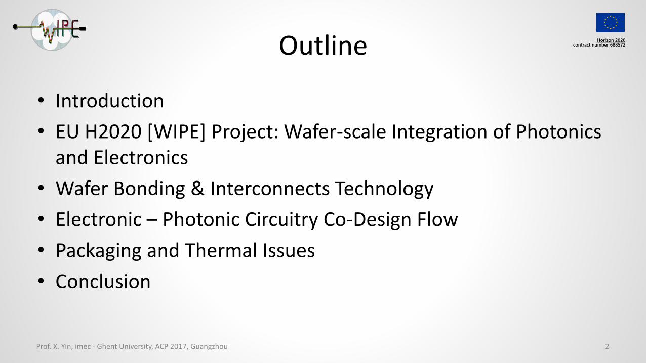
• Introduction
• EU H2020 [WIPE] Project: Wafer-scale Integration of Photonics and Electronics
• Wafer Bonding & Interconnects Technology
• Electronic – Photonic Circuitry Co-Design Flow
• Packaging and Thermal Issues
• Conclusion
2Prof. X. Yin, imec - Ghent University, ACP 2017, Guangzhou
Horizon 2020 contract number 688572The Connected Age
3
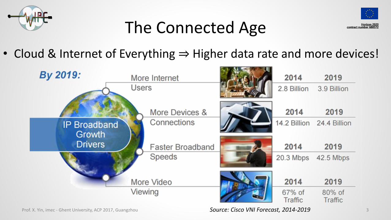
• Cloud & Internet of Everything ⇒ Higher data rate and more devices!
Source: Cisco VNI Forecast, 2014-2019
Horizon 2020 contract number 688572
Prof. X. Yin, imec - Ghent University, ACP 2017, Guangzhou
Horizon 2020 contract number 688572Clouds and Distributed Computing
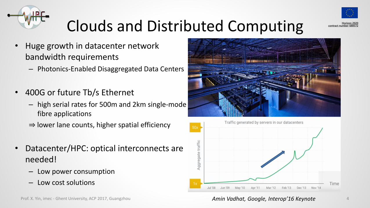
• Huge growth in datacenter network bandwidth requirements– Photonics-Enabled Disaggregated Data Centers
• 400G or future Tb/s Ethernet– high serial rates for 500m and 2km single-mode
fibre applications
⇒ lower lane counts, higher spatial efficiency
• Datacenter/HPC: optical interconnects are needed! – Low power consumption
– Low cost solutions
4Amin Vadhat, Google, Interop’16 KeynoteProf. X. Yin, imec - Ghent University, ACP 2017, Guangzhou

Horizon 2020 contract number 688572Transceiver Form Factors
5
12.4
41.5
107.5
9.5
21.5
92
8.5
18.35
70
9.5
40
102
8.5
18.35
75.913
22.58
100.4
100G products
400G products *Current commercial
Class I (1.5W) LPMClass II (2W)Class III (2.5W)Class IV (3.5W)Class V (4W)Class VI (4.5W)Class VII (5W)
LPM (1W)Class I (3.5W)Class II (7W)Class III(8W)Class IV (10W)Class V (12W)Class VI (14W)Class VII (16W)
LPM (1W)Class I (1.5W)Class II (3W)Class III (4.5W)Class IV (6W)Class V (7.5W)Class VI (9W)
Class I (2W) LPMClass II (4W)Class III (8W)Class IV (12W)Class V (16W)
LPM (2W)Class I (4W)Class II (8W)Class III (12W)*Class IV (16W)*Class V (20W)Class VI (24W)
LPM (2)Class I (3W)Class II (6W)Class III (9W)Class IV (12W)Class V (15W)Class VI (18W)
Pluggable transceivers with varying
dimensions and power classes
On board optics not included,
specs expected later in 2017
Dimensions in mm
Prof. X. Yin, imec - Ghent University, ACP 2017, Guangzhou

Horizon 2020 contract number 688572Power Dissipation in 400G Modules
6
Integrated Electronics/Photronics promise footprint/power consumption
improvements
OSFP
QSFP-DD
CFP8
Prof. X. Yin, imec - Ghent University, ACP 2017, Guangzhou

Horizon 2020 contract number 688572EU H2020 [WIPE] Project
7
WIPE in short
• Physical electronics-photonics (photronics) connection
• Novel co-design, connection and die attach flows
• Wafer-scale integration of silicon based electronic (Bi)CMOS and InP based photonic circuitry.
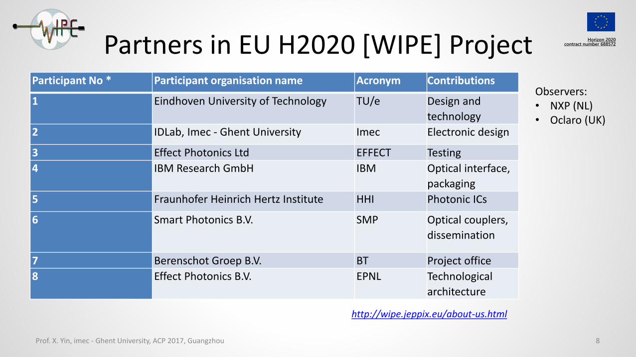
• 8 Partners and 2 Observers from Netherlands, Belgium, Germany, UK and Switzerland
http://wipe.jeppix.eu/about-us.html
Prof. X. Yin, imec - Ghent University, ACP 2017, Guangzhou
Horizon 2020 contract number 688572Partners in EU H2020 [WIPE] Project
8
http://wipe.jeppix.eu/about-us.html
Participant No * Participant organisation name Acronym Contributions
1 Eindhoven University of Technology TU/e Design and
technology
2 IDLab, Imec - Ghent University Imec Electronic design
3 Effect Photonics Ltd EFFECT Testing
4 IBM Research GmbH IBM Optical interface,
packaging
5 Fraunhofer Heinrich Hertz Institute HHI Photonic ICs
6 Smart Photonics B.V. SMP Optical couplers,
dissemination
7 Berenschot Groep B.V. BT Project office
8 Effect Photonics B.V. EPNL Technological
architecture
Observers:• NXP (NL)• Oclaro (UK)
Prof. X. Yin, imec - Ghent University, ACP 2017, Guangzhou
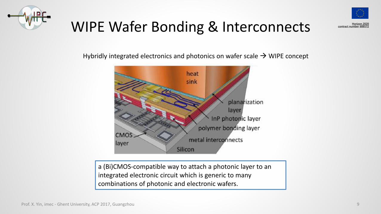
Horizon 2020 contract number 688572WIPE Wafer Bonding & Interconnects
9Prof. X. Yin, imec - Ghent University, ACP 2017, Guangzhou
a (Bi)CMOS-compatible way to attach a photonic layer to an integrated electronic circuit which is generic to many combinations of photonic and electronic wafers.
Hybridly integrated electronics and photonics on wafer scale WIPE concept

Horizon 2020 contract number 688572WIPE Wafer Bonding & Interconnects
10Prof. X. Yin, imec - Ghent University, ACP 2017, Guangzhou
p-InP
active material
Q1.06 (WG layer)
p- InP
Q1.3/ InGaAs etch stop layer
InP substrate

Horizon 2020 contract number 688572WIPE Wafer Bonding & Interconnects
11Prof. X. Yin, imec - Ghent University, ACP 2017, Guangzhou
EAM DFB SSC
Processing at HHI Single project wafer run
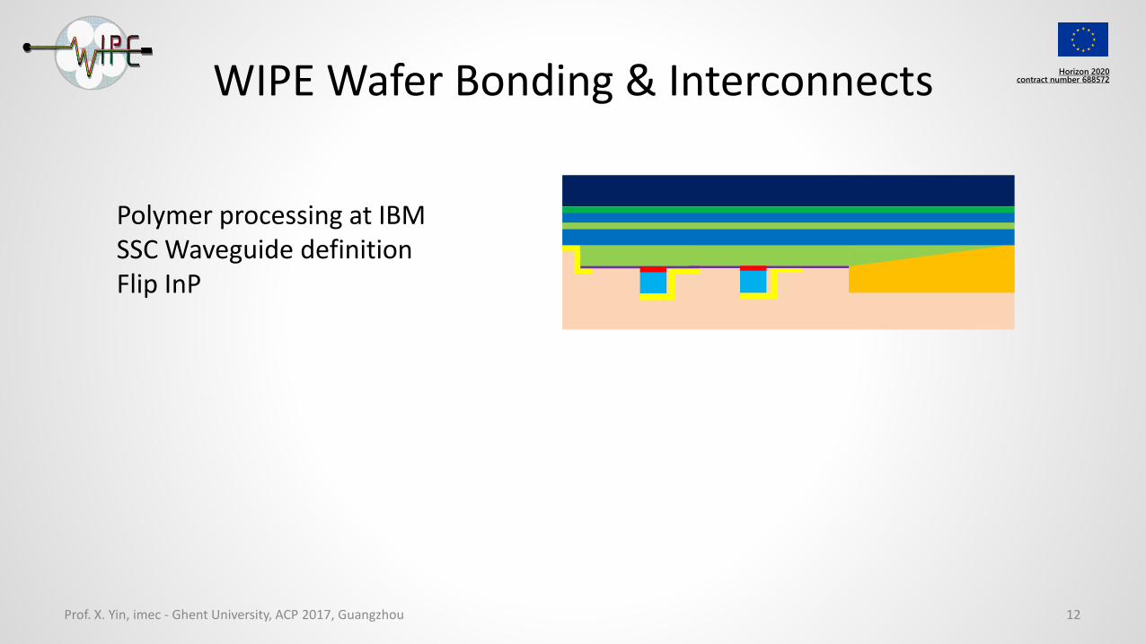
Horizon 2020 contract number 688572WIPE Wafer Bonding & Interconnects
12Prof. X. Yin, imec - Ghent University, ACP 2017, Guangzhou
Polymer processing at IBMSSC Waveguide definitionFlip InP

Horizon 2020 contract number 688572WIPE Wafer Bonding & Interconnects
13Prof. X. Yin, imec - Ghent University, ACP 2017, Guangzhou
BiCMOS wafer Marker backside InP wafer

Horizon 2020 contract number 688572WIPE Wafer Bonding & Interconnects
14Prof. X. Yin, imec - Ghent University, ACP 2017, Guangzhou
Bonding

Horizon 2020 contract number 688572WIPE Wafer Bonding & Interconnects
15Prof. X. Yin, imec - Ghent University, ACP 2017, Guangzhou
InP Substrate removal

Horizon 2020 contract number 688572WIPE Wafer Bonding & Interconnects
16Prof. X. Yin, imec - Ghent University, ACP 2017, Guangzhou
InP Substrate removal

Horizon 2020 contract number 688572WIPE Wafer Bonding & Interconnects
17Prof. X. Yin, imec - Ghent University, ACP 2017, Guangzhou
InP Substrate removal

Horizon 2020 contract number 688572Bonding & Interconnects: Initial Results
18Prof. X. Yin, imec - Ghent University, ACP 2017, Guangzhou
• Bonding test: top view on the result after substrate & etch stop removal ⇒ no cracks visible
• Interconnects: process realized with multi resist layer deposition and Fluoride-based dry etch ⇒ resistance in the order of 100 mOhm/cm
1.45 cm
116 μm

Horizon 2020 contract number 688572Co-Design: Challenge and Opportunity
19Prof. X. Yin, imec - Ghent University, ACP 2017, Guangzhou

Horizon 2020 contract number 688572WIPE Co-Design Tool Development
20
Specification
Platform selection
Building block/sub circuit design
Draft floor plan
Final layout
Verification
Packaging
EIC
PIC
Based on existing EIC and PIC design flows and
its interfaces, considering packaging aspects
EICPIC
Packaging
Mechanical
Thermal
Spec
RF
Optical Interface
Prof. X. Yin, imec - Ghent University, ACP 2017, Guangzhou

Horizon 2020 contract number 688572WIPE PIC Development
21
Gen. 0
Test Structures to
evaluate process flow
Gen. 1
Building block: EML
PD dark currentthermometer
PD avoids back reflections to DFB
Heater tunes DFB wavelength
Prof. X. Yin, imec - Ghent University, ACP 2017, Guangzhou

Horizon 2020 contract number 688572WIPE PIC Development
22
Gen. 0 Gen. 1
Test Structures to
evaluate process flow
Building block: PIN-PD
Optical Rx based on a rather conventional PIN photodiode (PD), connected to a SSC, BW > 35 GHz, 0.8 A/W at 1550nm
Prof. X. Yin, imec - Ghent University, ACP 2017, Guangzhou
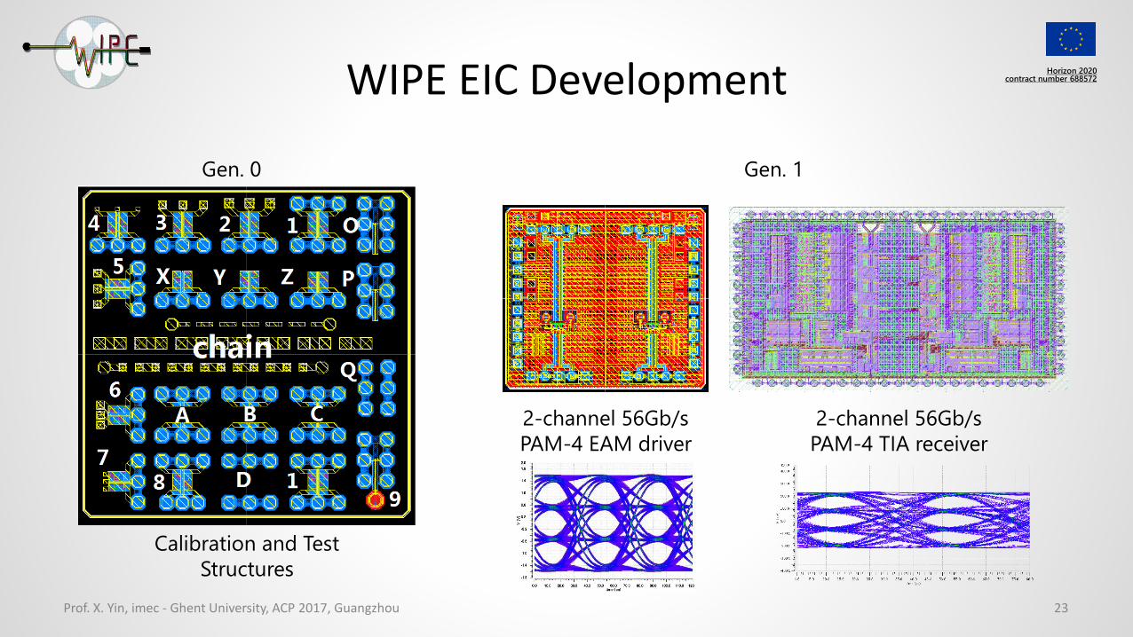
Horizon 2020 contract number 688572WIPE EIC Development
23
Gen. 0
Calibration and Test
Structures
Gen. 1
2-channel 56Gb/s
PAM-4 EAM driver
2-channel 56Gb/s
PAM-4 TIA receiver
Prof. X. Yin, imec - Ghent University, ACP 2017, Guangzhou
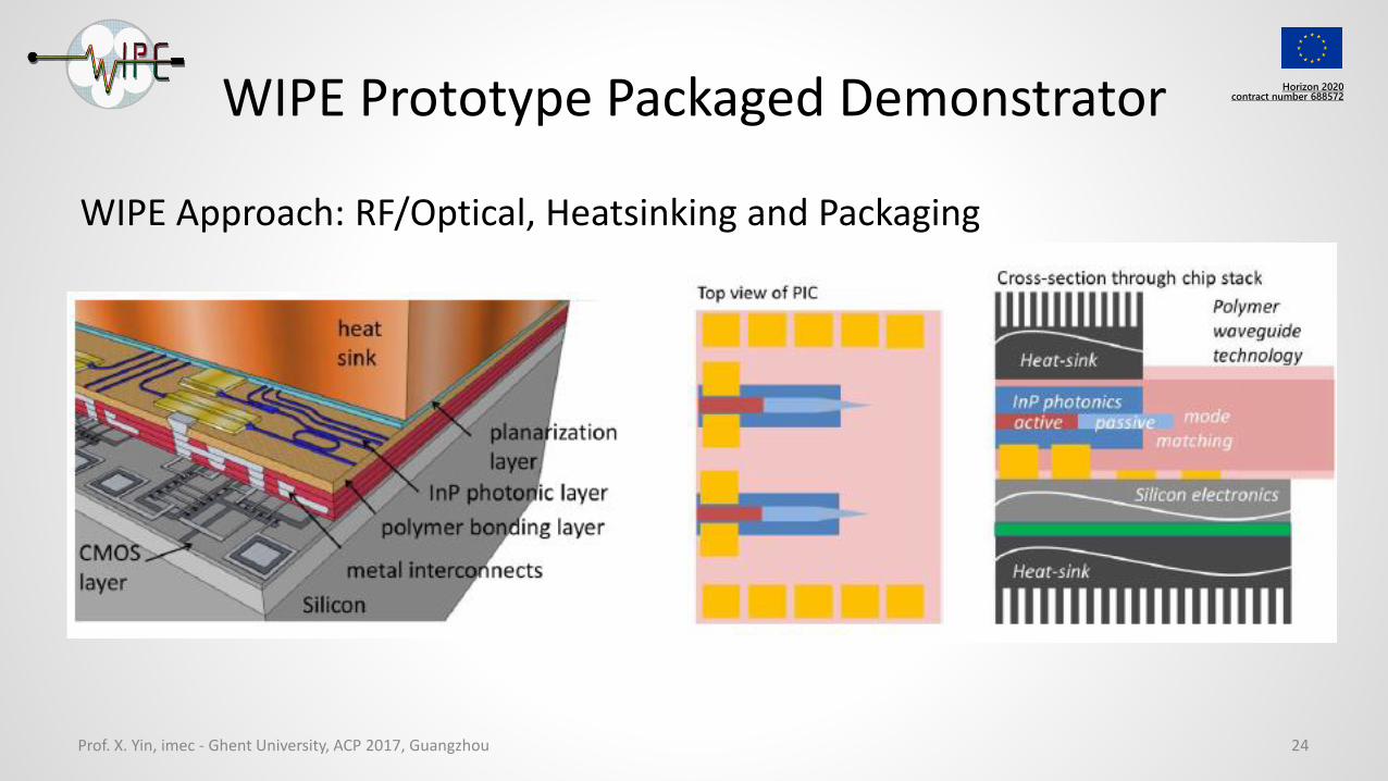
Horizon 2020 contract number 688572WIPE Prototype Packaged Demonstrator
24
WIPE Approach: RF/Optical, Heatsinking and Packaging
Prof. X. Yin, imec - Ghent University, ACP 2017, Guangzhou
Horizon 2020 contract number 688572
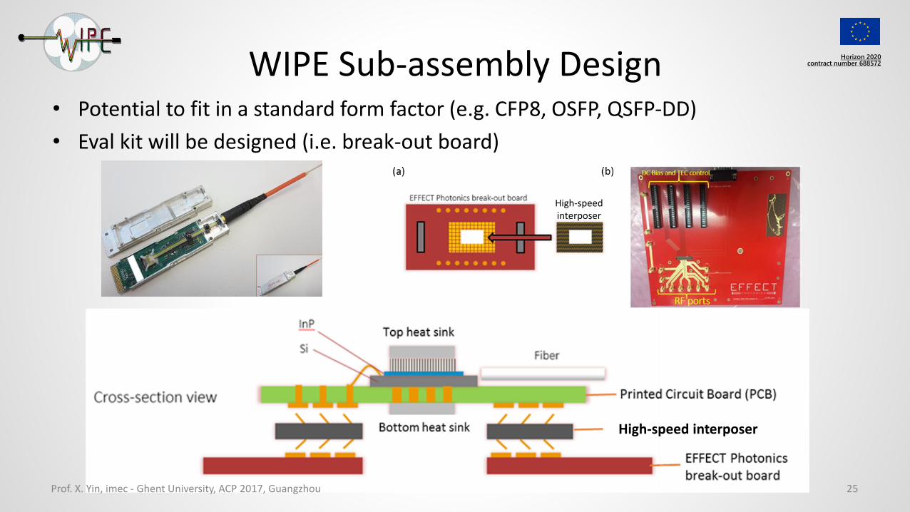
High-speed interposer
WIPE Sub-assembly Design
25
• Potential to fit in a standard form factor (e.g. CFP8, OSFP, QSFP-DD)
• Eval kit will be designed (i.e. break-out board)
Prof. X. Yin, imec - Ghent University, ACP 2017, Guangzhou
High-speed interposer
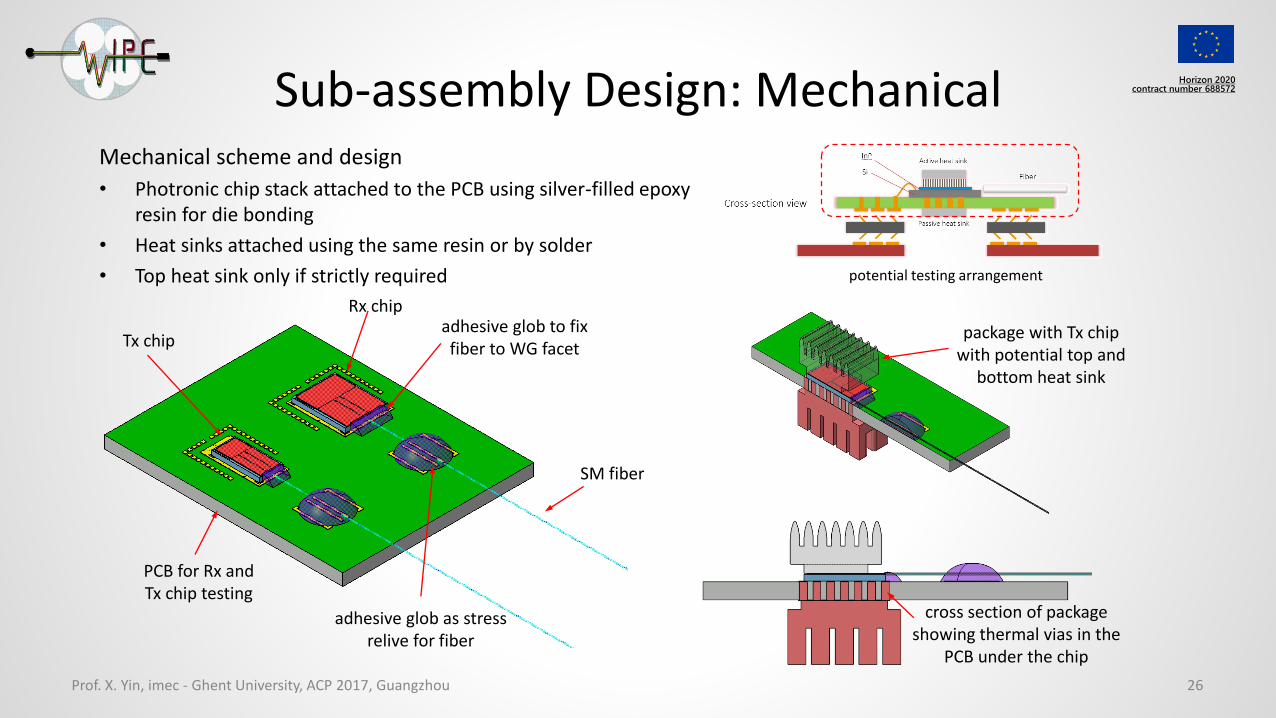
Horizon 2020 contract number 688572Sub-assembly Design: Mechanical
26
package with Tx chip with potential top and
bottom heat sink
potential testing arrangement
Mechanical scheme and design
• Photronic chip stack attached to the PCB using silver-filled epoxy resin for die bonding
• Heat sinks attached using the same resin or by solder
• Top heat sink only if strictly required
SM fiber
Rx chipadhesive glob to fix fiber to WG facet
PCB for Rx and Tx chip testing
adhesive glob as stress relive for fiber
Tx chip
cross section of package showing thermal vias in the
PCB under the chip
Prof. X. Yin, imec - Ghent University, ACP 2017, Guangzhou

Horizon 2020 contract number 688572Sub-assembly Design: Optical Connections
27Prof. X. Yin, imec - Ghent University, ACP 2017, Guangzhou
Challenge: Spot-size conversion
Solution: Adiabatic coupling
Advantages: High tolerance against
- positioning errors, Wavelength, Polarization
Low backreflection
Compatible with electrical assembly techniques
Polymer waveguideson carrier (or interposer)
SOI waveguideson chip
9mm
On-chip SOI waveguide
Single mode fiber core
Spot-size conversion
0.5 x 0.2mm
SToA: Coupling between Si photonics chip and SM fibers
A. La Porta et al., "Scalable Optical Coupling between Silicon Photonics Waveguides and Polymer Waveguides," 2016 IEEE 66th Electronic Components and Technology Conference (ECTC).

Horizon 2020 contract number 688572Sub-assembly Design: Optical Connections
28Prof. X. Yin, imec - Ghent University, ACP 2017, Guangzhou
Experimental demonstration of adiabatic coupling
Adiabatic coupling based on silicon waveguide tapering
Polymer waveguide and silicon waveguide are in contact
Reducing the silicon waveguide width forces the light to couple to the polymer waveguide
No additional components required Optical connection established during soldering
Silicon die, flip-chip attached to polymer waveguides
Silicon photonics chipIN
OUT
Cross-sections (side view and front view) of assembly after underfilling
Substrate of photonics chip
Substrate of polymer WGs
Epoxy
Lower claddingEpoxy underfillBuried oxide
Substrate of photonics chip
Lower cladding
Buried oxide + underfill
Poymer WG core
Ibrahim Murat Soganci, Antonio La Porta, and Bert Jan Offrein, "Flip-chip optical couplers with scalable I/O count for silicon photonics," Opt. Express 21, 16075-16085 (2013)

Horizon 2020 contract number 688572Sub-assembly Design: Optical Connections
29
• Only one single-mode (SM) fiber required for, respectively, the TX and RX chip
• Optical signals guided at the edge of the photronic chip by the SSC– SSC converter matches the mode-size between the mode in the InP to the one of the SM fiber
• Fiber placement by active optical alignment and subsequent fixation by low-shrinkage UV-curable adhesive resin
Prof. X. Yin, imec - Ghent University, ACP 2017, Guangzhou

Horizon 2020 contract number 688572Sub-assembly Design: Thermal
30
• Electronic IC needs to dissipate more power then the PIC
• PIC more temperature sensitive
• Polymer has low thermal conductivity
• Modeling with heat sinks attached, photronic assembled and attached to the PCB
• Heat maps:
Power map of Rx chip, electronic layer contains all heat
sources
Power map of Tx chip, heat sources are present in the
electronic and in the photonic layer
Prof. X. Yin, imec - Ghent University, ACP 2017, Guangzhou

Horizon 2020 contract number 688572Sub-assembly Design: Thermal (Cont’d)
31
• Heat transfer coefficient 10.000 W/(m2K)
• Heat maps– at the device plane for the silicon chip
– on the InP/polymer interface of photonic chip
• Averages and maxima relative temperatures are calculated over the entire Electrical IC and PIC
# layer material thickness thermal conductivity comment
[µm] [W/mK]
130 heat sink top Zn 2000 113-140 zinc die cast is standard for housing of QSFP connector
120 TIM top TC 5622 20 4.3 Thermal Interface Material, Dow Corning thermal paste
110 polymer Dow Corning 20 0.35 thermal conductivity ~25% of SiO2
100 InP InP 15 68 layer in the device is structured and could be thinner 5µm
10 polymer Dow Corning 10 0.35 thermal conductivity ~25% of SiO2
11 interconnect Au 20 310 20x20µm cross section embedded in layer 10&20
20 polymer Dow Corning 10 0.35 thermal conductivity ~25% of SiO2, includes air gaps as thermal barrier
200 Si Si 375 149
210 Ag filled epoxy H20E-HC 50 10.9 up to 23 W/mK if additional curing step of 1h@ 200°C
220 PCB laminate 1000 17 laminate with filled thermal vias, 4.5% Cu fillfraction (first estimation)
230 TIM bottom H20E-HC 50 10.9 see #210, interface can be soldered e.g. In#227 54 W/mK, BL >20µm
240 heat sink bottom Cu 4000 384 new heat sink, would be part of the casing
Prof. X. Yin, imec - Ghent University, ACP 2017, Guangzhou

Horizon 2020 contract number 688572Thermal Simulations: TX Chip
32
Summary of simulation results:
• Top heat sink in the PIC TX is required
• Two heat sinks of 5,000 W/(m2K) each seems to suffice
Temperature map of one half of the Tx chip showing the electronic layer
boundary (left) and the photonic layer boundary (right) applying a heat
transfer coefficient of 10.000 W/(m2K) to the boundaries. Tavg = 11.2
and 9.4. Tmax = 20.0 and 37.3, 2°C distance between contour lines
2D plot of heat transfer coefficient sweep for the top and bottom heat sink
up to 10000 W/(m²K) showing Tmax. Left for the electronic layer and right
for the photonic layer.Prof. X. Yin, imec - Ghent University, ACP 2017, Guangzhou

Horizon 2020 contract number 688572Thermal Simulations: RX Chip
33
Summary of simulation results:
• Top heat sink in the PIC RX can be avoided
• One (bottom) heat sink of 5,000 W/(m2K) seems to suffice
Temperature map of one half of the Rx chip showing the electronic
layer boundary (left) and the photonic layer boundary (right) applying a
heat trasfer coefficient of 10000 W/(m2K) to the boundaries. Tavg = 4.2
and 3.1. Tmax = 7.5 and 5.0 with 0.5°C distance between contour lines.
2D plot of heat transfer coefficient sweep for the top and bottom heat sink up to
10000 W/(m²K) showing Tmax. Left for the electronic layer and right for the
photonic layerProf. X. Yin, imec - Ghent University, ACP 2017, Guangzhou

Horizon 2020 contract number 688572WIPE Technological Architecture Outlook
34
Know-how to favour &
enable technology
adoption
Leveraging the
disruptive technology
Prof. X. Yin, imec - Ghent University, ACP 2017, Guangzhou

Horizon 2020 contract number 688572Conclusion
• Effective co-design and co-integration of photonics and electronics allows for miniaturization and subsequently energy and cost savings.
• We describe the EU H2020 WIPE approach towards photonic/electronic integrated circuitry co-design/co-optimization and wafer-scale integration.
• Initial results are promising and the WIPE technologies have potential to enable next-level photonic/electronic integration
35Prof. X. Yin, imec - Ghent University, ACP 2017, Guangzhou

Horizon 2020 contract number 688572
Thank you for your attention
Any Questions?
Contacts:
• Email: [email protected], [email protected]