Embed Size (px)
Citation preview

1 2017 Integrated Device Technology, Inc. All rights reserved. Product specifications subject to change without notice. DSC-4670/5©
NOVEMBER 2017
CMOS SuperSync FIFO™
8,192 x 1816,384 x 18
IDT72255LAIDT72265LA
IDT and the IDT logo are registered trademarks of Integrated Device Technology, Inc. SuperSync FIFO is a trademark of Integrated Device Technology, Inc
COMMERCIAL AND INDUSTRIAL TEMPERATURE RANGES
LEAD FINISH (SnPb) ARE IN EOL PROCESS - LAST TIME BUY EXPIRES JUNE 15, 2018FEATURES••••• Choose among the following memory organizations:
IDT72255LA — 8,192 x 18IDT72265LA — 16,384 x 18
••••• Pin-compatible with the IDT72275/72285 SuperSync FIFOs••••• 10ns read/write cycle time (8ns access time)••••• Fixed, low first word data latency time••••• Auto power down minimizes standby power consumption••••• Master Reset clears entire FIFO••••• Partial Reset clears data, but retains programmable settings••••• Retransmit operation with fixed, low first word data latency time••••• Empty, Full and Half-Full flags signal FIFO status••••• Programmable Almost-Empty and Almost-Full flags, each flag
can default to one of two preselected offsets••••• Program partial flags by either serial or parallel means••••• Select IDT Standard timing (using EF and FF flags) or First
Word Fall Through timing (using OR and IR flags)••••• Output enable puts data outputs into high impedance state••••• Easily expandable in depth and width••••• Independent Read and Write clocks (permit reading and writing
simultaneously)
••••• Available in the 64-pin Thin Quad Flat Pack (TQFP) and the 64-pin Slim Thin Quad Flat Pack (STQFP)
••••• High-performance submicron CMOS technology••••• Industrial temperature range (–40°C to +85°C) is available••••• Green parts available, see ordering information
DESCRIPTIONThe IDT72255LA/72265LA are exceptionally deep, high speed, CMOS
First-In-First-Out (FIFO) memories with clocked read and write controls. TheseFIFOs offer numerous improvements over previous SuperSync FIFOs,including the following:••••• The limitation of the frequency of one clock input with respect to the other has
been removed. The Frequency Select pin (FS) has been removed, thusit is no longer necessary to select which of the two clock inputs, RCLK orWCLK, is running at the higher frequency.
••••• The period required by the retransmit operation is now fixed and short.••••• The first word data latency period, from the time the first word is written to an
empty FIFO to the time it can be read, is now fixed and short. (The variableclock cycle counting delay associated with the latency period found onprevious SuperSync devices has been eliminated on this SuperSync family.)
INPUT REGISTER
OUTPUT REGISTER
RAM ARRAY8,192 x 1816,384 x 18
FLAGLOGIC
F F /IRPAFEF /ORPAEHF
READ POINTER
READCONTROL
LOGIC
WRITE CONTROLLOGIC
WRITE POINTER
RESETLOGIC
WEN WCLK D0 -D17LD
MRS
REN
RCLK
OEQ0 -Q17
OFFSET REGISTER
PRS
FWFT/SI
SEN
RT
4670 drw01
FUNCTIONAL BLOCK DIAGRAM

2
IDT72255LA/72265LA CMOS SuperSync FIFO™8,192 x 18 and 16,384 x 18
COMMERCIAL AND INDUSTRIALTEMPERATURE RANGES
PIN CONFIGURATIONS
TQFP (PN64, ORDER CODE: PF)STQFP (PP64, ORDER CODE: TF)
TOP VIEW
DESCRIPTION (CONTINUED)
PIN 1
12
345
67
89
101112
1314
1516
4847
464544
4342
4140
393837
3635
3433
WEN
SEN
DC
VCC
GND
D17
D16
D15
D14
D13
D12
D11
D10
D9
D8
D7
64 63 62 61 60 59 58 57 56 55 54 53 52 51 50 49
17 18 19 20 21 22 23 24 25 26 27 28 29 30 31 32
Q17Q16GNDQ15Q14VCC
Q13Q12Q11GNDQ10Q9Q8Q7Q6GND
WC
LKP
RS
MR
S
LD
FW
FT
/SI
GN
D
FF
/IR
PA
F
HF
VC
C
PA
E
EF
/OR
RC
LKR
EN
RT
OE
Q5
Q4
VC
C
Q3
Q2
GN
DQ
1
Q0
GN
DD0
D1
D2
D3D4
D5
D6
4670 drw02
SuperSync FIFOs are particularly appropriate for networking, video,telecommunications, data communications and other applications that need tobuffer large amounts of data.
The input port is controlled by a Write Clock (WCLK) input and a Write Enable(WEN) input. Data is written into the FIFO on every rising edge of WCLK whenWEN is asserted. The output port is controlled by a Read Clock (RCLK) inputand Read Enable (REN) input. Data is read from the FIFO on every rising edgeof RCLK when REN is asserted. An Output Enable (OE) input is provided forthree-state control of the outputs.
The frequencies of both the RCLK and the WCLK signals may vary from 0to fMAX with complete independence. There are no restrictions on the frequencyof one clock input with respect to the other.
There are two possible timing modes of operation with these devices: IDTStandard mode and First Word Fall Through (FWFT) mode.
In IDT Standard mode, the first word written to an empty FIFO will not appearon the data output lines unless a specific read operation is performed. A readoperation, which consists of activating REN and enabling a rising RCLK edge,will shift the word from internal memory to the data output lines.
NOTE:1. DC = Don’t Care. Must be tied to GND or VCC, cannot be left open.
3
IDT72255LA/72265LA CMOS SuperSync FIFO™8,192 x 18 and 16,384 x 18
COMMERCIAL AND INDUSTRIALTEMPERATURE RANGES
DESCRIPTION (CONTINUED)
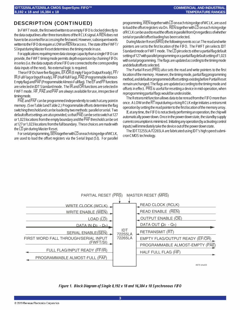
Figure 1. Block Diagram of Single 8,192 x 18 and 16,384 x 18 Synchronous FIFO
DATA OUT (Q0 - Qn)DATA IN (D0 - Dn)
MASTER RESET (MRS)
READ CLOCK (RCLK)
READ ENABLE (REN)
OUTPUT ENABLE (OE)
EMPTY FLAG/OUTPUT READY (EF/OR)
PROGRAMMABLE ALMOST-EMPTY (PAE)
WRITE CLOCK (WCLK)
WRITE ENABLE (WEN)
LOAD (LD)
FULL FLAG/INPUT READY (FF/IR)
PROGRAMMABLE ALMOST-FULL (PAF)
IDT72255LA72265LA
PARTIAL RESET (PRS)
FIRST WORD FALL THROUGH/SERIAL INPUT(FWFT/SI)
RETRANSMIT (RT)
4670 drw03
HALF FULL FLAG (HF)
SERIAL ENABLE(SEN)
In FWFT mode, the first word written to an empty FIFO is clocked directly tothe data output lines after three transitions of the RCLK signal. A REN does nothave to be asserted for accessing the first word. However, subsequent wordswritten to the FIFO do require a LOW on REN for access. The state of the FWFT/SI input during Master Reset determines the timing mode in use.
For applications requiring more data storage capacity than a single FIFO canprovide, the FWFT timing mode permits depth expansion by chaining FIFOsin series (i.e. the data outputs of one FIFO are connected to the correspondingdata inputs of the next). No external logic is required.
These FIFOs have five flag pins, EF/OR (Empty Flag or Output Ready), FF/IR (Full Flag or Input Ready), HF (Half-full Flag), PAE (Programmable Almost-Empty flag) and PAF (Programmable Almost-Full flag). The EF and FF functionsare selected in IDT Standard mode. The IR and OR functions are selected inFWFT mode. HF, PAE and PAF are always available for use, irrespective oftiming mode.
PAE and PAF can be programmed independently to switch at any point inmemory. (See Table I and Table 2.) Programmable offsets determine the flagswitching threshold and can be loaded by two methods: parallel or serial. Twodefault offset settings are also provided, so that PAE can be set to switch at 127or 1,023 locations from the empty boundary and the PAF threshold can be setat 127 or 1,023 locations from the full boundary. These choices are made withthe LD pin during Master Reset.
For serial programming, SEN together with LD on each rising edge of WCLK,are used to load the offset registers via the Serial Input (SI). For parallel
programming, WEN together with LD on each rising edge of WCLK, are usedto load the offset registers via Dn. REN together with LD on each rising edgeof RCLK can be used to read the offsets in parallel from Qn regardless of whetherserial or parallel offset loading has been selected.
During Master Reset (MRS) the following events occur: The read and writepointers are set to the first location of the FIFO. The FWFT pin selects IDTStandard mode or FWFT mode. The LD pin selects either a partial flag defaultsetting of 127 with parallel programming or a partial flag default setting of 1,023with serial programming. The flags are updated according to the timing modeand default offsets selected.
The Partial Reset (PRS) also sets the read and write pointers to the firstlocation of the memory. However, the timing mode, partial flag programmingmethod, and default or programmed offset settings existing before Partial Resetremain unchanged. The flags are updated according to the timing mode andoffsets in effect. PRS is useful for resetting a device in mid-operation, whenreprogramming partial flags would be undesirable.
The Retransmit function allows data to be reread from the FIFO more thanonce. A LOW on the RT input during a rising RCLK edge initiates a retransmitoperation by setting the read pointer to the first location of the memory array.
If, at any time, the FIFO is not actively performing an operation, the chip willautomatically power down. Once in the power down state, the standby supplycurrent consumption is minimized. Initiating any operation (by activating controlinputs) will immediately take the device out of the power down state.
The IDT72255LA/72265LA are fabricated using IDT’s high speed submi-cron CMOS technology.

4
IDT72255LA/72265LA CMOS SuperSync FIFO™8,192 x 18 and 16,384 x 18
COMMERCIAL AND INDUSTRIALTEMPERATURE RANGES
Symbol Name I/O DescriptionD0–D17 Data Inputs I Data inputs for a 18-bit bus.MRS Master Reset I MRS initializes the read and write pointers to zero and sets the output register to all zeroes. During
Master Reset, the FIFO is configured for either FWFT or IDT Standard mode, one of two programmable flag default settings, and serial or parallel programming of the offset settings.
PRS Partial Reset I PRS initializes the read and write pointers to zero and sets the output register to all zeroes. DuringPartial Reset, the existing mode (IDT or FWFT), programming method (serial or parallel), andprogrammable flag settings are all retained.
RT Retransmit I RT asserted on the rising edge of RCLK initializes the READ pointer to zero, sets the EF flag toLOW (OR to HIGH in FWFT mode) temporarily and does not disturb the write pointer, programmingmethod, existing timing mode or programmable flag settings. RT is useful to reread data from the firstphysical location of the FIFO.
FWFT/SI First Word Fall I During Master Reset, selects First Word Fall Through or IDT Standard mode. After Master Reset,Through/Serial In this pin functions as a serial input for loading offset registers.
WCLK Write Clock I When enabled by WEN, the rising edge of WCLK writes data into the FIFO and offsets into theprogrammable registers for parallel programming, and when enabled by SEN, the rising edge ofWCLK writes one bit of data into the programmable register for serial programming.
WEN Write Enable I WEN enables WCLK for writing data into the FIFO memory and offset registers.RCLK Read Clock I When enabled by REN, the rising edge of RCLK reads data from the FIFO memory and offsets from
the programmable registers.REN Read Enable I REN enables RCLK for reading data from the FIFO memory and offset registers.OE Output Enable I OE controls the output impedance of Qn.
SEN Serial Enable I SEN enables serial loading of programmable flag offsets.LD Load I During Master Reset, LD selects one of two partial flag default offsets (127 or 1,023) and determines
the flag offset programming method, serial or parallel. After Master Reset, this pin enables writing toand reading from the offset registers.
DC Don't Care I This pin must be tied to either VCC or GND and must not toggle after Master Reset.FF/IR Full Flag/ O In the IDT Standard mode, the FF function is selected. FF indicates whether or not the FIFO
Input Ready memory is full. In the FWFT mode, the IR function is selected. IR indicates whether or notthere is space available for writing to the FIFO memory.
EF/OR Empty Flag/ O In the IDT Standard mode, the EF function is selected. EF indicates whether or not the FIFOOutput Ready memory is empty. In FWFT mode, the OR function is selected. OR indicates whether or not there is
valid data available at the outputs.PAF Programmable O PAF goes LOW if the number of words in the FIFO memory is more than total word capacity of the
Almost-Full Flag FIFO minus the full offset value m, which is stored in the Full Offset register. There are two possibledefault values for m: 127 or 1,023.
PAE Programmable O PAE goes LOW if the number of words in the FIFO memory is less than offset n, which is stored inAlmost-Empty Flag the Empty Offset register. There are two possible default values for n: 127 or 1,023. Other values
for n can be programmed into the device. HF Half-Full Flag O HF indicates whether the FIFO memory is more or less than half-full.Q0–Q17 Data Outputs O Data outputs for an 18-bit bus.VCC Power +5 Volt power supply pins.GND Ground Ground pins.
PIN DESCRIPTION

5
IDT72255LA/72265LA CMOS SuperSync FIFO™8,192 x 18 and 16,384 x 18
COMMERCIAL AND INDUSTRIALTEMPERATURE RANGES
Symbol Parameter(1) Conditions Max. UnitCIN(2) Input VIN = 0V 10 pF
CapacitanceCOUT(1,2) Output VOUT = 0V 10 pF
Capacitance
Symbol Rating Com’l & Ind’l UnitVTERM Terminal Voltage –0.5 to +7.0 V
with respect to GNDTSTG Storage –55 to +125 °C
TemperatureIOUT DC Output Current –50 to +50 mA
NOTES:1. With output deselected, (OE ≥ VIH).2. Characterized values, not currently tested.
DC ELECTRICAL CHARACTERISTICS(Commercial: VCC = 5V ± 10%, TA = 0°C to +70°C; Industrial: VCC = 5V ± 10%, TA = -40°C to +85°C)
NOTE:1. 1.5V undershoots are allowed for 10ns once per cycle.
IDT72255LAIDT72265LA
Commercial & Industrial(1)
tCLK = 10, 15, 20 ns
Symbol Parameter Min. Max. UnitILI(2) Input Leakage Current –1 1 µAILO(3) Output Leakage Current –10 10 µAVOH Output Logic “1” Voltage, IOH = –2 mA 2.4 — VVOL Output Logic “0” Voltage, IOL = 8 mA — 0.4 VICC1(4,5,6) Active Power Supply Current — 80 mAICC2(4,7) Standby Current — 20 mA
NOTES:1. Industrial temperature range product for 15ns and 20ns speed grades are available as a standard device.2. Measurements with 0.4 ≤ VIN ≤ VCC.3. OE ≥ VIH, 0.4 ≤ VOUT ≤ VCC.4. Tested with outputs disabled (IOUT = 0).5. RCLK and WCLK toggle at 20 MHz and data inputs switch at 10 MHz.6. Typical ICC1 = 15 + 2.1*fS + 0.02*CL*fS (in mA) with VCC = 5V, TA = 25°C, fS = WCLK frequency = RCLK frequency (in MHz, using TTL levels), data
switching at fS/2, CL = capacitive load (in pF).7. All Inputs = VCC –0.2V or GND + 0.2V, except RCLK and WCLK, which toggle at 20 MHz.
NOTE:1. Stresses greater than those listed under ABSOLUTE MAXIMUM RATINGS may cause
permanent damage to the device. This is a stress rating only and functional operationof the device at these or any other conditions above those indicated in the operationalsections of this specification is not implied. Exposure to absolute maximum ratingconditions for extended periods may affect reliability.
ABSOLUTE MAXIMUM RATINGS RECOMMENDED DC OPERATINGCONDITIONS
CAPACITANCE (TA = +25°C, f = 1.0MHz)
Symbol Parameter Min. Typ. Max. UnitVCC Supply Voltage (Com’l/Ind’l) 4.0 5.0 5.5 V
GND Supply Voltage (Com’l/Ind’l) 0 0 0 VVIH Input High Voltage (Com’l/Ind’l) 2.0 ⎯ — V
VIL(1) Input Low Voltage (Com’l/Ind’l) ⎯ ⎯ 0.8 VTA Operating Temperature 0 ⎯ +70 °C
CommercialTA Operating Temperature -40 ⎯ +85 °C
Industrial
6
IDT72255LA/72265LA CMOS SuperSync FIFO™8,192 x 18 and 16,384 x 18
COMMERCIAL AND INDUSTRIALTEMPERATURE RANGES
4670 drw04
1.1K
30pF*680Ω
5V
D.U.T.
* Includes jig and scope capacitances.
Input Pulse Levels GND to 3.0VInput Rise/Fall Times 3nsInput Timing Reference Levels 1.5VOutput Reference Levels 1.5VOutput Load See Figure 2
AC TEST CONDITIONS
NOTES:1. All AC timings apply to both Standard IDT mode and First Word Fall Through mode.2. Industrial temperature range product for 15ns and 20ns speed grades are available as a standard device.3. Pulse widths less than minimum values are not allowed.4. Values guaranteed by design, not currently tested.
Figure 2. Output Load
Commercial Commercial & Industrial(2)
IDT72255LA10 IDT72255LA15 IDT72255LA20IDT72265LA10 IDT72265LA15 IDT72265LA20
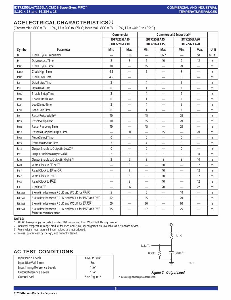
Symbol Parameter Min. Max. Min. Max. Min. Max. UnitfS Clock Cycle Frequency — 100 — 66.7 — 50 MHztA Data Access Time 2 8 2 10 2 12 nstCLK Clock Cycle Time 10 — 15 — 20 — nstCLKH Clock High Time 4.5 — 6 — 8 — nstCLKL Clock Low Time 4.5 — 6 — 8 — nstDS Data Setup Time 3 — 4 — 5 — nstDH Data Hold Time 0 — 1 — 1 — nstENS Enable Setup Time 3 — 4 — 5 — nstENH Enable Hold Time 0 — 1 — 1 — nstLDS Load Setup Time 3 — 4 — 5 — nstLDH Load Hold Time 0 — 1 — 1 — nstRS Reset Pulse Width(3) 10 — 15 — 20 — nstRSS Reset Setup Time 10 — 15 — 20 — nstRSR Reset Recovery Time 10 — 15 — 20 — nstRSF Reset to Flag and Output Time — 10 — 15 — 20 nstFWFT Mode Select Time 0 — 0 — 0 — nstRTS Retransmit Setup Time 3 — 4 — 5 — nstOLZ Output Enable to Output in Low Z(4) 0 — 0 — 0 — nstOE Output Enable to Output Valid 2 6 3 8 3 10 nstOHZ Output Enable to Output in High Z(4) 2 6 3 8 3 10 nstWFF Write Clock to FF or IR — 8 — 10 — 12 nstREF Read Clock to EF or OR — 8 — 10 — 12 nstPAF Write Clock to PAF — 8 — 10 — 12 nstPAE Read Clock to PAE — 8 — 10 — 12 nstHF Clock to HF — 16 — 20 — 22 nstSKEW1 Skew time between RCLK and WCLK for FF/IR 5 — 6 — 10 — nstSKEW2 Skew time between RCLK and WCLK for PAE and PAF 12 — 15 — 20 — nstSKEW3 Skew time between RCLK and WCLK for EF/OR 60 — 60 — 60 — nstSKEW4 Skew time between RCLK and WCLK for PAE and PAF 15 — 17 — 25 — ns
for Re-transmit operation
AC ELECTRICAL CHARACTERISTICS(1)
(Commercial: VCC = 5V ± 10%, TA = 0°C to +70°C; Industrial: VCC = 5V ± 10%, TA = –40°C to +85°C)
7
IDT72255LA/72265LA CMOS SuperSync FIFO™8,192 x 18 and 16,384 x 18
COMMERCIAL AND INDUSTRIALTEMPERATURE RANGES
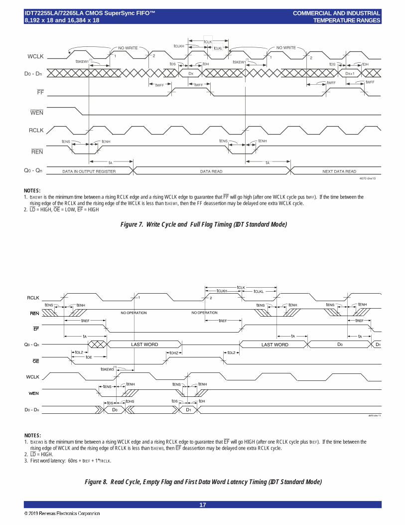
If the FIFO is full, the first read operation will cause FF to go HIGH.Subsequent read operations will cause PAF and HF to go HIGH at theconditions described in Table 1. If further read operations occur, withoutwrite operations, PAE will go LOW when there are n words in the FIFO,where n is the empty offset value. Continuing read operations will cause theFIFO to become empty. When the last word has been read from the FIFO,the EF will go LOW inhibiting further read operations. REN isignored when the FIFO is empty.
When configured in IDT Standard mode, the EF and FF outputs aredouble register-buffered outputs.
Relevant timing diagrams for IDT Standard mode can be found inFigure 7, 8 and 11.
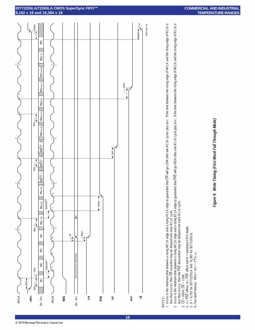
FIRST WORD FALL THROUGH MODE (FWFT)In this mode, the status flags, IR, PAF, HF, PAE, and OR operate in the
manner outlined in Table 2. To write data into to the FIFO, WEN must beLOW. Data presented to the DATA IN lines will be clocked into the FIFO onsubsequent transitions of WCLK. After the first write is performed, the OutputReady (OR) flag will go LOW. Subsequent writes will continue to fill up theFIFO. PAE will go HIGH after n + 2 words have been loaded into the FIFO,where n is the empty offset value. The default setting for this value is statedin the footnote of Table 2. This parameter is also user programmable. Seesection on Programmable Flag Offset Loading.
If one continued to write data into the FIFO, and we assumed no readoperations were taking place, the HF would toggle to LOW once the 4,098thword for the IDT72255LA and 8,194th word for the IDT72265LA, respec-tively was written into the FIFO. Continuing to write data into the FIFO willcause the PAF to go LOW. Again, if no reads are performed, the PAF willgo LOW after (8,193-m) writes for the IDT72255LA and (16,385-m) writesfor the IDT72265LA, where m is the full offset value. The default setting forthis value is stated in the footnote of Table 2.
When the FIFO is full, the Input Ready (IR) flag will go HIGH, inhibitingfurther write operations. If no reads are performed after a reset, IR will goHIGH after D writes to the FIFO. D = 8,193 writes for the IDT72255LA and16,385 writes for the IDT72265LA, respectively. Note that the additionalword in FWFT mode is due to the capacity of the memory plus outputregister.
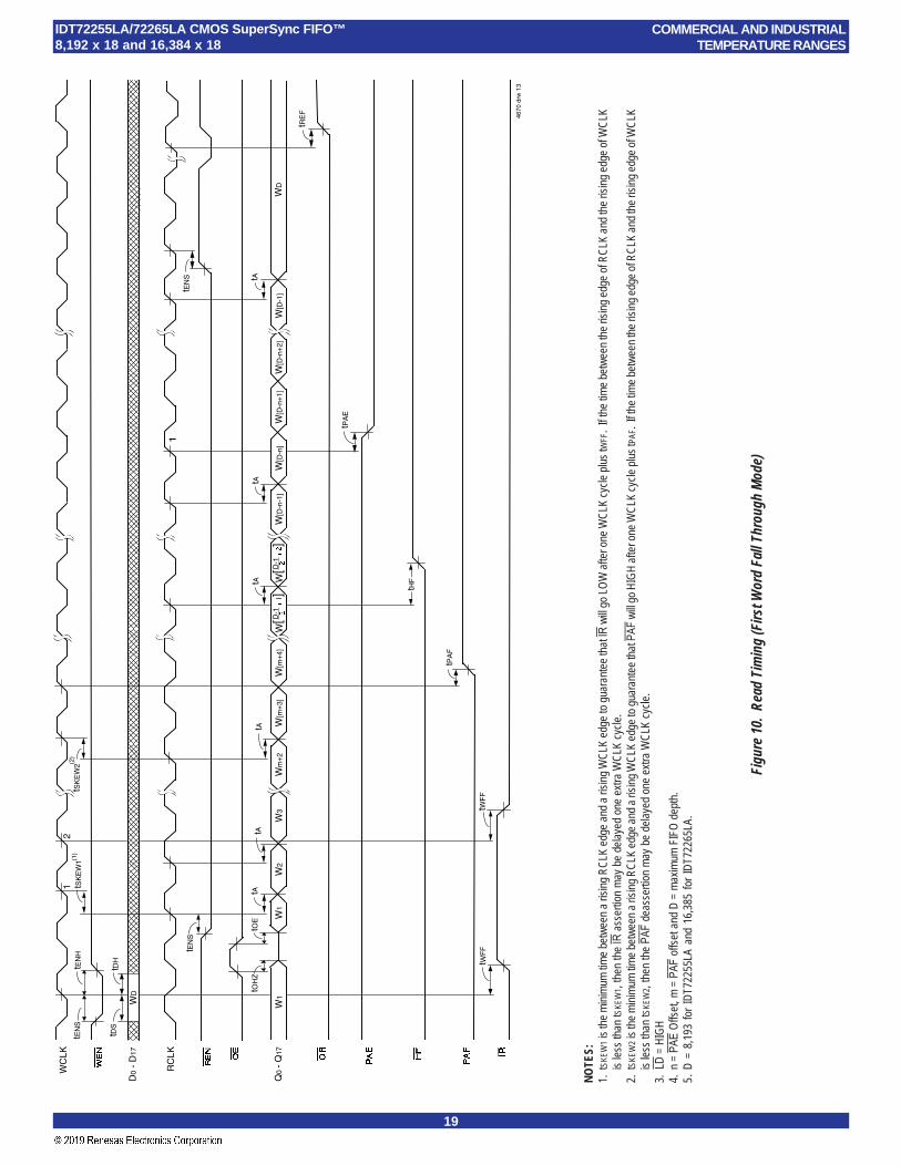
If the FIFO is full, the first read operation will cause the IR flag to go LOW.Subsequent read operations will cause the PAF and HF to go HIGH at theconditions described in Table 2. If further read operations occur, withoutwrite operations, the PAE will go LOW when there are n + 1 words in theFIFO, where n is the empty offset value. Continuing read operations willcause the FIFO to become empty. When the last word has been read fromthe FIFO, OR will go HIGH inhibiting further read operations. REN is ig-nored when the FIFO is empty.
When configured in FWFT mode, the OR flag output is triple register-buffered, and the IR flag output is double register-buffered.
Relevant timing diagrams for FWFT mode can be found in Figure 9, 10and 12.
FUNCTIONAL DESCRIPTION
TIMING MODES: IDT STANDARD vs FIRST WORD FALL THROUGH(FWFT) MODE
The IDT72255LA/72265LA support two different timing modes ofoperation: IDT Standard mode or First Word Fall Through (FWFT) mode.The selection of which mode will operate is determined during Master Re-set, by the state of the FWFT/SI input.
If, at the time of Master Reset, FWFT/SI is LOW, then IDT Standard modewill be selected. This mode uses the Empty Flag (EF) to indicate whetheror not there are any words present in the FIFO. It also uses the Full Flagfunction (FF) to indicate whether or not the FIFO has any free space forwriting. In IDT Standard mode, every word read from the FIFO, includingthe first, must be requested using the Read Enable (REN) and RCLK.
If, at the time of Master Reset, FWFT/SI is HIGH, then FWFT mode willbe selected. This mode uses Output Ready (OR) to indicate whether or notthere is valid data at the data outputs (Qn). It also uses Input Ready (IR) toindicate whether or not the FIFO has any free space for writing. In theFWFT mode, the first word written to an empty FIFO goes directly to Qnafter three RCLK rising edges, REN = LOW is not necessary. Subsequentwords must be accessed using the Read Enable (REN) and RCLK.
Various signals, both input and output signals operate differently depend-ing on which timing mode is in effect.
IDT STANDARD MODEIn this mode, the status flags, FF, PAF, HF, PAE, and EF operate in the
manner outlined in Table 1. To write data into to the FIFO, Write Enable(WEN) must be LOW. Data presented to the DATA IN lines will be clockedinto the FIFO on subsequent transitions of the Write Clock (WCLK). After thefirst write is performed, the Empty Flag (EF) will go HIGH. Subsequentwrites will continue to fill up the FIFO. The Programmable Almost-Empty flag(PAE) will go HIGH after n + 1 words have been loaded into the FIFO,where n is the empty offset value. The default setting for this value is statedin the footnote of Table 1. This parameter is also user programmable. Seesection on Programmable Flag Offset Loading.
If one continued to write data into the FIFO, and we assumed no readoperations were taking place, the Half-Full flag (HF) would toggle to LOWonce the 4,097th word for IDT72255LA and 8,193th word for IDT72265LArespectively was written into the FIFO. Continuing to write data into theFIFO will cause the Programmable Almost-Full flag (PAF) to go LOW.Again, if no reads are performed, the PAF will go LOW after (8,192-m)writes for the IDT72255LA and (16,384-m) writes for the IDT72265LA.The offset “m” is the full offset value. The default setting for this value isstated in the footnote of Table 1. This parameter is also user programmable.See section on Programmable Flag Offset Loading.
When the FIFO is full, the Full Flag (FF) will go LOW, inhibiting furtherwrite operations. If no reads are performed after a reset, FF will go LOWafter D writes to the FIFO. D = 8,192 writes for the IDT72255LA and16,384 for the IDT72265LA, respectively.
8
IDT72255LA/72265LA CMOS SuperSync FIFO™8,192 x 18 and 16,384 x 18
COMMERCIAL AND INDUSTRIALTEMPERATURE RANGES
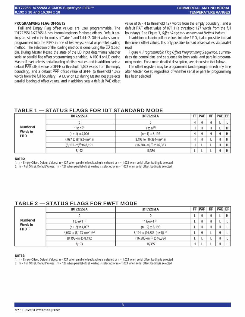
PROGRAMMING FLAG OFFSETSFull and Empty Flag offset values are user programmable. The
IDT72255LA/72265LA has internal registers for these offsets. Default set-tings are stated in the footnotes of Table 1 and Table 2. Offset values can beprogrammed into the FIFO in one of two ways; serial or parallel loadingmethod. The selection of the loading method is done using the LD (Load)pin. During Master Reset, the state of the LD input determines whetherserial or parallel flag offset programming is enabled. A HIGH on LD duringMaster Reset selects serial loading of offset values and in addition, sets adefault PAE offset value of 3FFH (a threshold 1,023 words from the emptyboundary), and a default PAF offset value of 3FFH (a threshold 1,023words from the full boundary). A LOW on LD during Master Reset selectsparallel loading of offset values, and in addition, sets a default PAE offset
IDT72255LA IDT72265LA FF PAF HF PAE EF
0 0 H H H L L1 to n (1) 1 to n (1) H H H L H
(n + 1) to 4,096 (n + 1) to 8,192 H H H H H4,097 to (8,192–(m+1)) 8,193 to (16,384–(m+1)) H H L H H(8,192–m)(2) to 8,191 (16,384–m) (2) to 16,383 H L L H H
8,192 16,384 L L L H H
NOTES:1. n = Empty Offset, Default Values: n = 127 when parallel offset loading is selected or n = 1,023 when serial offset loading is selected.2. m = Full Offset, Default Values: m = 127 when parallel offset loading is selected or m = 1,023 when serial offset loading is selected.
TABLE 1 — STATUS FLAGS FOR IDT STANDARD MODE
Number ofWords inFIFO
IDT72255LA IDT72265LA FF PAF HF PAE EF
0 0 L H H L H1 to n+1 (1) 1 to n+1 (1) L H H L L
(n + 2) to 4,097 (n + 2) to 8,193 L H H H L4,098 to (8,193–(m+1))(2) 8,194 to (16,385–(m+1)) (2) L H L H L
(8,193–m) to 8,192 (16,385–m) (2) to 16,384 L L L H L8,193 16,385 H L L H L
NOTES:1. n = Empty Offset, Default Values: n = 127 when parallel offset loading is selected or n = 1,023 when serial offset loading is selected.2. m = Full Offset, Default Values: m = 127 when parallel offset loading is selected or m = 1,023 when serial offset loading is selected.
TABLE 2 — STATUS FLAGS FOR FWFT MODE
Number ofWords inFIFO (1)
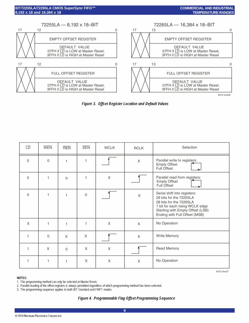
value of 07FH (a threshold 127 words from the empty boundary), and adefault PAF offset value of 07FH (a threshold 127 words from the fullboundary). See Figure 3, Offset Register Location and Default Values.
In addition to loading offset values into the FIFO, it also possible to readthe current offset values. It is only possible to read offset values via parallelread.
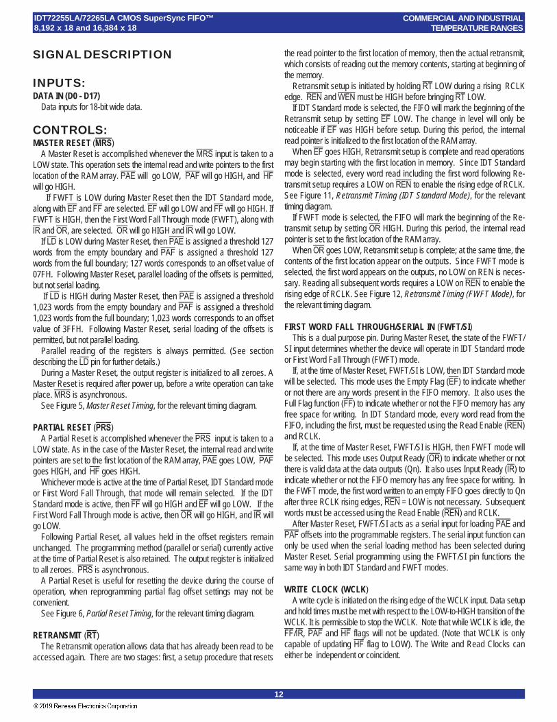
Figure 4, Programmable Flag Offset Programming Sequence, summa-rizes the control pins and sequence for both serial and parallel program-ming modes. For a more detailed description, see discussion that follows.
The offset registers may be programmed (and reprogrammed) any timeafter Master Reset, regardless of whether serial or parallel programminghas been selected.
9
IDT72255LA/72265LA CMOS SuperSync FIFO™8,192 x 18 and 16,384 x 18
COMMERCIAL AND INDUSTRIALTEMPERATURE RANGES
Figure 4. Programmable Flag Offset Programming Sequence
NOTES:1. The programming method can only be selected at Master Reset.2. Parallel reading of the offset registers is always permitted regardless of which programming method has been selected.3. The programming sequence applies to both IDT Standard and FWFT modes.
Figure 3. Offset Register Location and Default Values
EMPTY OFFSET REGISTER
17 0
07FH if LD is LOW at Master Reset,3FFH if LD is HIGH at Master Reset
FULL OFFSET REGISTER
17 0
DEFAULT VALUE
DEFAULT VALUE 07FH if LD is LOW at Master Reset,3FFH if LD is HIGH at Master Reset
12
1272255LA — 8,192 x 18–BIT
4670 drw06
EMPTY OFFSET REGISTER
17 0
07FH if LD is LOW at Master Reset,3FFH if LD is HIGH at Master Reset
FULL OFFSET REGISTER
17 0
DEFAULT VALUE
DEFAULT VALUE 07FH if LD is LOW at Master Reset,3FFH if LD is HIGH at Master Reset
13
1372265LA — 16,384 x 18–BIT
Selection
Parallel write to registers:Empty OffsetFull Offset
Parallel read from registers:Empty OffsetFull Offset
No Operation
Write Memory
Read Memory
No Operation
4670 drw07
LD
0
0
X
1
1
1
0
WEN
0
1
1
0
X
1
1
REN
1
0
1
X
0
1
1 Serial shift into registers:26 bits for the 72255LA28 bits for the 72265LA
SEN
1
1
1
X
X
X
0
WCLK
X
X
X
X
RCLK
X
X
X
X
X
1 bit for each rising WCLK edgeStarting with Empty Offset (LSB)Ending with Full Offset (MSB)

10
IDT72255LA/72265LA CMOS SuperSync FIFO™8,192 x 18 and 16,384 x 18
COMMERCIAL AND INDUSTRIALTEMPERATURE RANGES
SERIAL PROGRAMMING MODEIf Serial Programming mode has been selected, as described above, then
programming of PAE and PAF values can be achieved by using a combi-nation of the LD, SEN, WCLK and SI input pins. Programming PAE andPAF proceeds as follows: when LD and SEN are set LOW, data on theSI input are written, one bit for each WCLK rising edge, starting with theEmpty Offset LSB and ending with the Full Offset MSB. A total of 26 bits forthe IDT72255LA and 28 bits for the IDT72265LA. See Figure 13, SerialLoading of Programmable Flag Registers, for the timing diagram for thismode.
Using the serial method, individual registers cannot be programmed se-lectively. PAE and PAF can show a valid status only after the completeset of bits (for all offset registers) has been entered. The registers can bereprogrammed as long as the complete set of new offset bits is entered.When LD is LOW and SEN is HIGH, no serial write to the registers canoccur.
Write operations to the FIFO are allowed before and during the serialprogramming sequence. In this case, the programming of all offset bits doesnot have to occur at once. A select number of bits can be written to the SIinput and then, by bringing LD and SEN HIGH, data can be written toFIFO memory via Dn by toggling WEN. When WEN is brought HIGH withLD and SEN restored to a LOW, the next offset bit in sequence is written tothe registers via SI. If an interruption of serial programming is desired, it issufficient either to set LD LOW and deactivate SEN or to set SEN LOWand deactivate LD. Once LD and SEN are both restored to a LOW level,serial offset programming continues.
From the time serial programming has begun, neither partial flag will bevalid until the full set of bits required to fill all the offset registers has beenwritten. Measuring from the rising WCLK edge that achieves the abovecriteria; PAF will be valid after two more rising WCLK edges plus tPAF,PAE will be valid after the next two rising RCLK edges plus tPAE plustSKEW2.
It is not possible to read the flag offset values in a serial mode.
PARALLEL MODEIf Parallel Programming mode has been selected, as described above,
then programming of PAE and PAF values can be achieved by using acombination of the LD, WCLK , WEN and Dn input pins. ProgrammingPAEand PAF proceeds as follows: when LD and WEN are set LOW, data onthe inputs Dn are written into the Empty Offset Register on the first LOW-to-HIGH transition of WCLK. Upon the second LOW-to-HIGH transition of WCLK,data are written into the Full Offset Register. The third transition of WCLKwrites, once again, to the Empty Offset Register. See Figure 14, ParallelLoading of Programmable Flag Registers, for the timing diagram for thismode.
The act of writing offsets in parallel employs a dedicated write offsetregister pointer. The act of reading offsets employs a dedicated read offsetregister pointer. The two pointers operate independently; however, a readand a write should not be performed simultaneously to the offset registers.A Master Reset initializes both pointers to the Empty Offset (LSB) register.A Partial Reset has no effect on the position of these pointers.
Write operations to the FIFO are allowed before and during the parallelprogramming sequence. In this case, the programming of all offsetregisters does not have to occur at one time. One, two or more offset reg-isters can be written and then by bringing LD HIGH, write operations canbe redirected to the FIFO memory. When LD is set LOW again, and WENis LOW, the next offset register in sequence is written to. As an
alternative to holding WEN LOW and toggling LD, parallel programmingcan also be interrupted by setting LD LOW and toggling WEN.
Note that the status of a partial flag (PAE or PAF) output is invalid dur-ing the programming process. From the time parallel programming hasbegun, a partial flag output will not be valid until the appropriate offset wordhas been written to the register(s) pertaining to that flag. Measuring fromthe rising WCLK edge that achieves the above criteria; PAF will be validafter two more rising WCLK edges plus tPAF, PAE will be valid after thenext two rising RCLK edges plus tPAE plus tSKEW2.
The act of reading the offset registers employs a dedicated read offsetregister pointer. The contents of the offset registers can be read on the Q0-Qn pins when LD is set LOW and REN is set LOW. Data are read via Qnfrom the Empty Offset Register on the first LOW-to-HIGH transition of RCLK.Upon the second LOW-to-HIGH transition of RCLK, data are read from theFull Offset Register. The third transition of RCLK reads, once again, fromthe Empty Offset Register. See Figure 15, Parallel Read of ProgrammableFlag Registers, for the timing diagram for this mode.
It is permissible to interrupt the offset register read sequence with readsor writes to the FIFO. The interruption is accomplished by deasserting REN,LD, or both together. When REN and LD are restored to a LOW level,reading of the offset registers continues where it left off. It should be noted,and care should be taken from the fact that when a parallel read of the flagoffsets is performed, the data word that was present on the output lines Qnwill be overwritten.
Parallel reading of the offset registers is always permitted regardless ofwhich timing mode (IDT Standard or FWFT modes) has been selected.
RETRANSMIT OPERATIONThe Retransmit operation allows data that has already been read to be
accessed again. There are two stages: first, a setup procedure that resetsthe read pointer to the first location of memory, then the actual retransmit,which consists of reading out the memory contents, starting at thebeginning of memory.
Retransmit setup is initiated by holding RT LOW during a rising RCLKedge. REN and WEN must be HIGH before bringing RT LOW. At leastone word, but no more than D - 2 words should have been written into theFIFO between Reset (Master or Partial) and the time of Retransmit setup.D = 8,192 for the IDT72255LA and D = 16,384 for the IDT72265LA. InFWFT mode, D = 8,193 for the IDT72255LA and D = 16,385 for theIDT72265LA.
If IDT Standard mode is selected, the FIFO will mark the beginning ofthe Retransmit setup by setting EF LOW. The change in level will only benoticeable if EF was HIGH before setup. During this period, the internalread pointer is initialized to the first location of the RAM array.
When EF goes HIGH, Retransmit setup is complete and read opera-tions may begin starting with the first location in memory. Since IDT Stan-dard mode is selected, every word read including the first word followingRetransmit setup requires a LOW on REN to enable the rising edge ofRCLK. See Figure 11, Retransmit Timing (IDT Standard Mode), for therelevant timing diagram.
If FWFT mode is selected, the FIFO will mark the beginning of theRetransmit setup by setting OR HIGH. During this period, the internal readpointer is set to the first location of the RAM array.
When OR goes LOW, Retransmit setup is complete; at the same time,the contents of the first location appear on the outputs. Since FWFT modeis selected, the first word appears on the outputs, no LOW on REN isnecessary. Reading all subsequent words requires a LOW on REN to

11
IDT72255LA/72265LA CMOS SuperSync FIFO™8,192 x 18 and 16,384 x 18
COMMERCIAL AND INDUSTRIALTEMPERATURE RANGES
enable the rising edge of RCLK. See Figure 12, Retransmit Timing (FWFTMode), for the relevant timing diagram.
For either IDT Standard mode or FWFT mode, updating of the PAE,HF and PAF flags begin with the rising edge of RCLK that RT is setup.PAE is synchronized to RCLK, thus on the second rising edge of RCLK
after RT is setup, the PAE flag will be updated. HF is asynchronous, thusthe rising edge of RCLK that RT is setup will update HF. PAF is synchro-nized to WCLK, thus the second rising edge of WCLK that occurs tSKEWafter the rising edge of RCLK that RT is setup will update PAF. RT issynchronized to RCLK.
12
IDT72255LA/72265LA CMOS SuperSync FIFO™8,192 x 18 and 16,384 x 18
COMMERCIAL AND INDUSTRIALTEMPERATURE RANGES
SIGNAL DESCRIPTION
INPUTS:DATA IN (D0 - D17)
Data inputs for 18-bit wide data.
CONTROLS:MASTER RESET (MRS)
A Master Reset is accomplished whenever the MRS input is taken to aLOW state. This operation sets the internal read and write pointers to the firstlocation of the RAM array. PAE will go LOW, PAF will go HIGH, and HFwill go HIGH.
If FWFT is LOW during Master Reset then the IDT Standard mode,along with EF and FF are selected. EF will go LOW and FF will go HIGH. IfFWFT is HIGH, then the First Word Fall Through mode (FWFT), along withIR and OR, are selected. OR will go HIGH and IR will go LOW.
If LD is LOW during Master Reset, then PAE is assigned a threshold 127words from the empty boundary and PAF is assigned a threshold 127words from the full boundary; 127 words corresponds to an offset value of07FH. Following Master Reset, parallel loading of the offsets is permitted,but not serial loading.
If LD is HIGH during Master Reset, then PAE is assigned a threshold1,023 words from the empty boundary and PAF is assigned a threshold1,023 words from the full boundary; 1,023 words corresponds to an offsetvalue of 3FFH. Following Master Reset, serial loading of the offsets ispermitted, but not parallel loading.
Parallel reading of the registers is always permitted. (See sectiondescribing the LD pin for further details.)
During a Master Reset, the output register is initialized to all zeroes. AMaster Reset is required after power up, before a write operation can takeplace. MRS is asynchronous.
See Figure 5, Master Reset Timing, for the relevant timing diagram.
PARTIAL RESET (PRS)A Partial Reset is accomplished whenever the PRS input is taken to a
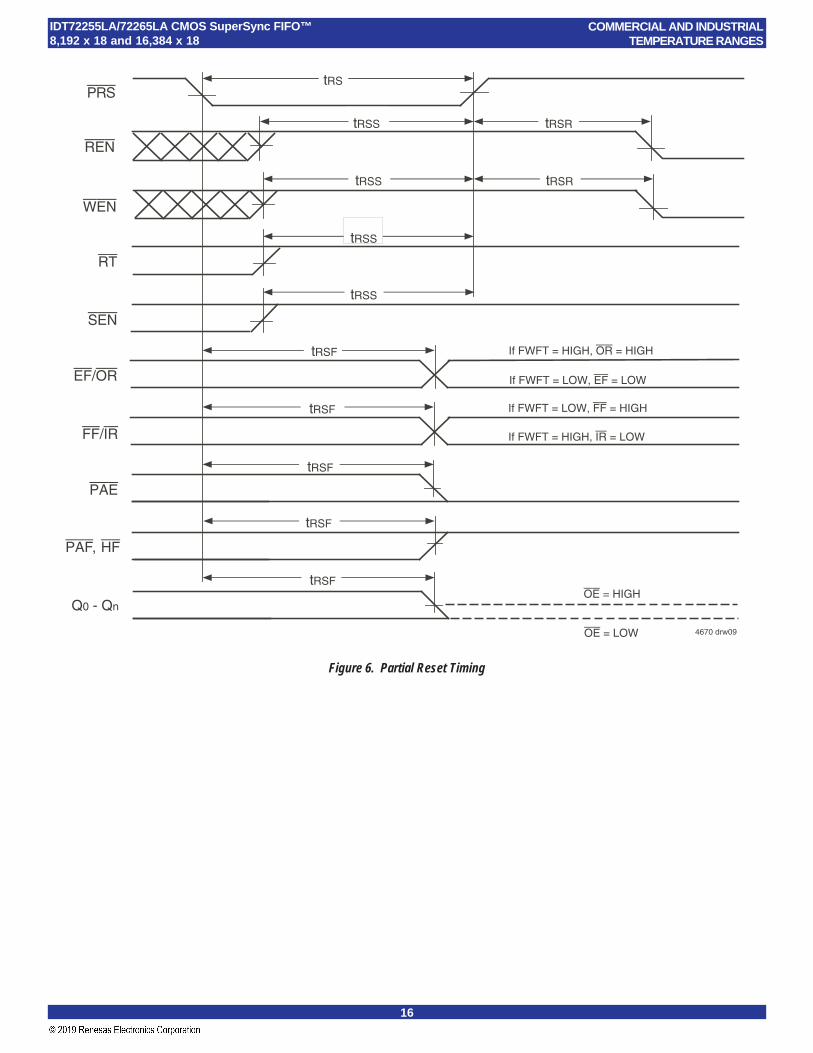
LOW state. As in the case of the Master Reset, the internal read and writepointers are set to the first location of the RAM array, PAE goes LOW, PAFgoes HIGH, and HF goes HIGH.
Whichever mode is active at the time of Partial Reset, IDT Standard modeor First Word Fall Through, that mode will remain selected. If the IDTStandard mode is active, then FF will go HIGH and EF will go LOW. If theFirst Word Fall Through mode is active, then OR will go HIGH, and IR willgo LOW.
Following Partial Reset, all values held in the offset registers remainunchanged. The programming method (parallel or serial) currently activeat the time of Partial Reset is also retained. The output register is initializedto all zeroes. PRS is asynchronous.
A Partial Reset is useful for resetting the device during the course ofoperation, when reprogramming partial flag offset settings may not beconvenient.
See Figure 6, Partial Reset Timing, for the relevant timing diagram.
RETRANSMIT (RT)The Retransmit operation allows data that has already been read to be
accessed again. There are two stages: first, a setup procedure that resets
the read pointer to the first location of memory, then the actual retransmit,which consists of reading out the memory contents, starting at beginning ofthe memory.
Retransmit setup is initiated by holding RT LOW during a rising RCLKedge. REN and WEN must be HIGH before bringing RT LOW.
If IDT Standard mode is selected, the FIFO will mark the beginning of theRetransmit setup by setting EF LOW. The change in level will only benoticeable if EF was HIGH before setup. During this period, the internalread pointer is initialized to the first location of the RAM array.
When EF goes HIGH, Retransmit setup is complete and read operationsmay begin starting with the first location in memory. Since IDT Standardmode is selected, every word read including the first word following Re-transmit setup requires a LOW on REN to enable the rising edge of RCLK.See Figure 11, Retransmit Timing (IDT Standard Mode), for the relevanttiming diagram.
If FWFT mode is selected, the FIFO will mark the beginning of the Re-transmit setup by setting OR HIGH. During this period, the internal readpointer is set to the first location of the RAM array.
When OR goes LOW, Retransmit setup is complete; at the same time, thecontents of the first location appear on the outputs. Since FWFT mode isselected, the first word appears on the outputs, no LOW on REN is neces-sary. Reading all subsequent words requires a LOW on REN to enable therising edge of RCLK. See Figure 12, Retransmit Timing (FWFT Mode), forthe relevant timing diagram.
FIRST WORD FALL THROUGH/SERIAL IN (FWFT/SI)This is a dual purpose pin. During Master Reset, the state of the FWFT/
SI input determines whether the device will operate in IDT Standard modeor First Word Fall Through (FWFT) mode.
If, at the time of Master Reset, FWFT/SI is LOW, then IDT Standard modewill be selected. This mode uses the Empty Flag (EF) to indicate whetheror not there are any words present in the FIFO memory. It also uses theFull Flag function (FF) to indicate whether or not the FIFO memory has anyfree space for writing. In IDT Standard mode, every word read from theFIFO, including the first, must be requested using the Read Enable (REN)and RCLK.
If, at the time of Master Reset, FWFT/SI is HIGH, then FWFT mode willbe selected. This mode uses Output Ready (OR) to indicate whether or notthere is valid data at the data outputs (Qn). It also uses Input Ready (IR) toindicate whether or not the FIFO memory has any free space for writing. Inthe FWFT mode, the first word written to an empty FIFO goes directly to Qnafter three RCLK rising edges, REN = LOW is not necessary. Subsequentwords must be accessed using the Read Enable (REN) and RCLK.
After Master Reset, FWFT/SI acts as a serial input for loading PAE andPAF offsets into the programmable registers. The serial input function canonly be used when the serial loading method has been selected duringMaster Reset. Serial programming using the FWFT/SI pin functions thesame way in both IDT Standard and FWFT modes.
WRITE CLOCK (WCLK)A write cycle is initiated on the rising edge of the WCLK input. Data setup
and hold times must be met with respect to the LOW-to-HIGH transition of theWCLK. It is permissible to stop the WCLK. Note that while WCLK is idle, theFF/IR, PAF and HF flags will not be updated. (Note that WCLK is onlycapable of updating HF flag to LOW). The Write and Read Clocks caneither be independent or coincident.

13
IDT72255LA/72265LA CMOS SuperSync FIFO™8,192 x 18 and 16,384 x 18
COMMERCIAL AND INDUSTRIALTEMPERATURE RANGES
WRITE ENABLE (WEN)When the WEN input is LOW, data may be loaded into the FIFO RAM
array on the rising edge of every WCLK cycle if the device is not full. Datais stored in the RAM array sequentially and independently of any ongoingread operation.
When WEN is HIGH, no new data is written in the RAM array on eachWCLK cycle.
To prevent data overflow in the IDT Standard mode, FF will go LOW,inhibiting further write operations. Upon the completion of a valid read cycle,FF will go HIGH allowing a write to occur. The FF is updated by two WCLKcycles + tSKEW after the RCLK cycle.
To prevent data overflow in the FWFT mode, IR will go HIGH, inhibitingfurther write operations. Upon the completion of a valid read cycle, IR willgo LOW allowing a write to occur. The IR flag is updated by two WCLKcycles + tSKEW after the valid RCLK cycle.
WEN is ignored when the FIFO is full in either FWFT or IDT Standardmode.
READ CLOCK (RCLK)A read cycle is initiated on the rising edge of the RCLK input. Data can
be read on the outputs, on the rising edge of the RCLK input. It is permis-sible to stop the RCLK. Note that while RCLK is idle, the EF/OR, PAE andHF flags will not be updated. (Note that RCLK is only capable of updatingthe HF flag to HIGH). The Write and Read Clocks can be independent orcoincident.
READ ENABLE (REN)When Read Enable is LOW, data is loaded from the RAM array into the
output register on the rising edge of every RCLK cycle if the device is notempty.
When the REN input is HIGH, the output register holds the previous dataand no new data is loaded into the output register. The data outputs Q0-Qnmaintain the previous data value.
In the IDT Standard mode, every word accessed at Qn, including the firstword written to an empty FIFO, must be requested using REN. When thelast word has been read from the FIFO, the Empty Flag (EF) will go LOW,inhibiting further read operations. REN is ignored when the FIFO is empty.Once a write is performed, EF will go HIGH allowing a read to occur. TheEF flag is updated by two RCLK cycles + tSKEW after the valid WCLK cycle.
In the FWFT mode, the first word written to an empty FIFO automaticallygoes to the outputs Qn, on the third valid LOW to HIGH transition of RCLK +tSKEW after the first write. REN does not need to be asserted LOW. In orderto access all other words, a read must be executed using REN. The RCLKLOW to HIGH transition after the last word has been read from the FIFO,Output Ready (OR) will go HIGH with a true read (RCLK with REN =LOW), inhibiting further read operations. REN is ignored when the FIFO isempty.
SERIAL ENABLE (SEN)The SEN input is an enable used only for serial programming of the
offset registers. The serial programming method must be selected duringMaster Reset. SEN is always used in conjunction with LD. When these linesare both LOW, data at the SI input can be loaded into the program registerone bit for each LOW-to-HIGH transition of WCLK. (See Figure 4.)
When SEN is HIGH, the programmable registers retains the previoussettings and no offsets are loaded. SEN functions the same way in both IDTStandard and FWFT modes.
OUTPUT ENABLE (OE)When Output Enable is enabled (LOW), the parallel output buffers
receive data from the output register. When OE is HIGH, the output databus (Qn) goes into a high impedance state.
LOAD (LD)This is a dual purpose pin. During Master Reset, the state of the LD
input determines one of two default offset values (127 or 1,023) for the PAEand PAF flags, along with the method by which these offset registers can beprogrammed, parallel or serial. After Master Reset, LD enables write op-erations to and read operations from the offset registers. Only the offsetloading method currently selected can be used to write to the registers.Offset registers can be read only in parallel. A LOW on LD during MasterReset selects a default PAE offset value of 07FH (a threshold 127 wordsfrom the empty boundary), a default PAF offset value of 07FH (a threshold127 words from the full boundary), and parallel loading of other offsetvalues. A HIGH on LD during Master Reset selects a default PAE offsetvalue of 3FFH (a threshold 1,023 words from the empty boundary), adefault PAF offset value of 3FFH (a threshold 1,023 words from the fullboundary), and serial loading of other offset values.
After Master Reset, the LD pin is used to activate the programmingprocess of the flag offset values PAE and PAF. Pulling LD LOW will begin aserial loading or parallel load or read of these offset values. See Figure 4,Programmable Flag Offset Programming Sequence.
OUTPUTS:FULL FLAG (FF/IR)
This is a dual purpose pin. In IDT Standard mode, the Full Flag (FF)function is selected. When the FIFO is full, FF will go LOW, inhibiting furtherwrite operations. When FF is HIGH, the FIFO is not full. If no reads areperformed after a reset (either MRS or PRS), FF will go LOW after D writesto the FIFO (D = 8,192 for the IDT72255LA and 16,384 for theIDT72265LA). See Figure 7, Write Cycle and Full Flag Timing (IDT Stan-dard Mode), for the relevant timing information.
In FWFT mode, the Input Ready (IR) function is selected. IR goes LOWwhen memory space is available for writing in data. When there is nolonger any free space left, IR goes HIGH, inhibiting further write operations.If no reads are performed after a reset (either MRS or PRS), IR will goHIGH after D writes to the FIFO (D = 8,193 for the IDT72255LA and 16,385for the IDT72265LA) See Figure 9, Write Timing (FWFT Mode), for therelevant timing information.
The IR status not only measures the contents of the FIFO memory, butalso counts the presence of a word in the output register. Thus, in FWFTmode, the total number of writes necessary to deassert IR is one greaterthan needed to assert FF in IDT Standard mode.
FF/IR is synchronous and updated on the rising edge of WCLK. FF/IRare double register-buffered outputs.
EMPTY FLAG (EF/OR)This is a dual purpose pin. In the IDT Standard mode, the Empty Flag
(EF) function is selected. When the FIFO is empty, EF will go LOW,inhibiting further read operations. When EF is HIGH, the FIFO is not empty.See Figure 8, Read Cycle, Empty Flag and First Word Latency Timing(IDT Standard Mode), for the relevant timing information.
In FWFT mode, the Output Ready (OR) function is selected. OR goesLOW at the same time that the first word written to an empty FIFO appearsvalid on the outputs. OR stays LOW after the RCLK LOW to HIGH transition
14
IDT72255LA/72265LA CMOS SuperSync FIFO™8,192 x 18 and 16,384 x 18
COMMERCIAL AND INDUSTRIALTEMPERATURE RANGES
that shifts the last word from the FIFO memory to the outputs. OR goesHIGH only with a true read (RCLK with REN = LOW). The previous datastays at the outputs, indicating the last word was read. Further data readsare inhibited until OR goes LOW again. See Figure 10, Read Timing(FWFT Mode), for the relevant timing information.
EF/OR is synchronous and updated on the rising edge of RCLK.In IDT Standard mode, EF is a double register-buffered output. In FWFT
mode, OR is a triple register-buffered output.
PROGRAMMABLE ALMOST-FULL FLAG (PAF)The Programmable Almost-Full flag (PAF) will go LOW when the FIFO
reaches the almost-full condition. In IDT Standard mode, if no reads areperformed after reset (MRS), PAF will go LOW after (D - m) words arewritten to the FIFO. The PAF will go LOW after (8,192-m) writes for theIDT72255LA and (16,384-m) writes for the IDT72265LA. The offset “m” isthe full offset value. The default setting for this value is stated in the footnoteof Table 1.
In FWFT mode, the PAF will go LOW after (8,193-m) writes for theIDT72255LA and (16,385-m) writes for the IDT72265LA, where m is thefull offset value. The default setting for this value is stated in the footnote ofTable 2.
See Figure 16, Programmable Almost-Full Flag Timing (IDT Standardand FWFT Mode), for the relevant timing information.
PAF is synchronous and updated on the rising edge of WCLK.
PROGRAMMABLE ALMOST-EMPTY FLAG (PAE)The Programmable Almost-Empty flag (PAE) will go LOW when the FIFO
reaches the almost-empty condition. In IDT Standard mode, PAE will go
LOW when there are n words or less in the FIFO. The offset “n” is theempty offset value. The default setting for this value is stated in the footnoteof Table 1.
In FWFT mode, the PAE will go LOW when there are n+1 words or lessin the FIFO. The default setting for this value is stated in the footnote ofTable 2.
See Figure 17, Programmable Almost-Empty Flag Timing (IDT Stan-dard and FWFT Mode), for the relevant timing information.
PAE is synchronous and updated on the rising edge of RCLK.
HALF-FULL FLAG (HF)This output indicates a half-full FIFO. The rising WCLK edge that fills the
FIFO beyond half-full sets HF LOW. The flag remains LOW until the differ-ence between the write and read pointers becomes less than or equal tohalf of the total depth of the device; the rising RCLK edge that accomplishesthis condition sets HF HIGH.
In IDT Standard mode, if no reads are performed after reset (MRS orPRS), HF will go LOW after (D/2 + 1) writes to the FIFO, where D = 8,192for the IDT72255LA and 16,384 for the IDT72265LA.
In FWFT mode, if no reads are performed after reset (MRS or PRS), HFwill go LOW after (D-1/2 + 2) writes to the FIFO, where D = 8,193 for theIDT72255LA and 16,385 for the IDT72265LA.
See Figure 18, Half-Full Flag Timing (IDT Standard and FWFT Modes),for the relevant timing information. Because HF is updated by both RCLKand WCLK, it is considered asynchronous.
DATA OUTPUTS (Q0-Q17)(Q0 - Q17) are data outputs for 18-bit wide data.
15
IDT72255LA/72265LA CMOS SuperSync FIFO™8,192 x 18 and 16,384 x 18
COMMERCIAL AND INDUSTRIALTEMPERATURE RANGES
Figure 5. Master Reset Timing
tRSMRS
tRSR
REN
tRSS
FWFT/SI
4670 drw08
tRSRtFWFT
tRSR
WEN
tRSS
LD
tRSRtRSS
tRSS
RT
SEN
tRSS
tRSF
tRSF
OE = HIGH
OE = LOW
PAE
PAF, HF
Q0 - Qn
tRSF
EF/OR
FF/IR
tRSF
tRSF If FWFT = HIGH, OR = HIGH
If FWFT = LOW, EF = LOW
If FWFT = LOW, FF = HIGH
If FWFT = HIGH, IR = LOW
16
IDT72255LA/72265LA CMOS SuperSync FIFO™8,192 x 18 and 16,384 x 18
COMMERCIAL AND INDUSTRIALTEMPERATURE RANGES
Figure 6. Partial Reset Timing
tRSPRS
tRSR
REN
tRSS
4670 drw09
tRSR
WEN
tRSS
RT
SEN
tRSS
tRSF
tRSF
OE = HIGH
OE = LOW
PAE
PAF, HF
Q0 - Qn
tRSF
EF/OR
FF/IR
tRSF
tRSF If FWFT = HIGH, OR = HIGH
If FWFT = LOW, EF = LOW
If FWFT = LOW, FF = HIGH
If FWFT = HIGH, IR = LOW
tRSS
17
IDT72255LA/72265LA CMOS SuperSync FIFO™8,192 x 18 and 16,384 x 18
COMMERCIAL AND INDUSTRIALTEMPERATURE RANGES
Figure 8. Read Cycle, Empty Flag and First Data Word Latency Timing (IDT Standard Mode)
NOTES:1. tSKEW3 is the minimum time between a rising WCLK edge and a rising RCLK edge to guarantee that EF will go HIGH (after one RCLK cycle plus tREF). If the time between the
rising edge of WCLK and the rising edge of RCLK is less than tSKEW3, then EF deassertion may be delayed one extra RCLK cycle.2. LD = HIGH.3. First word latency: 60ns + tREF + 1*TRCLK.
NOTES:1. tSKEW1 is the minimum time between a rising RCLK edge and a rising WCLK edge to guarantee that FF will go high (after one WCLK cycle pus tWFF). If the time between the
rising edge of the RCLK and the rising edge of the WCLK is less than tSKEW1, then the FF deassertion may be delayed one extra WCLK cycle.2. LD = HIGH, OE = LOW, EF = HIGH
Figure 7. Write Cycle and Full Flag Timing (IDT Standard Mode)
D0 - Dn
WEN
RCLK
FF
REN
tENH tENH
Q0 - Qn DATA READ NEXT DATA READDATA IN OUTPUT REGISTER
tSKEW1(1)
4670 drw10
WCLK
NO WRITE
1 2 1 2
tDS
NO WRITE
tWFFtWFFtWFF
tA
tENS tENS
tSKEW1(1)
tDS
tA
DX
tDH
tCLKtCLKH tCLKL
DX+1
tWFF
tDH
NO OPERATION
RCLK
4670 drw 11
tCLKtCLKH tCLKL
tENH
tREF
tA
tOLZtOE
Q0 - Qn
WCLK
(1)tSKEW3
D0 - Dn
tENS
tENStENH
tDS tDHS
D0
1 2
tOLZ
NO OPERATION
LAST WORD D0 D1
D1
tENS tENH
tDS tDH
tOHZ
LAST WORD
tREF
tENHtENS
tA tA
tREF
tENS tENH
18
IDT72255LA/72265LA CMOS SuperSync FIFO™8,192 x 18 and 16,384 x 18
COMMERCIAL AND INDUSTRIALTEMPERATURE RANGES
Figu
re 9.
Writ
e Tim
ing
(Firs
t Wor
d Fa
ll Thr
ough
Mod
e)
NOTE
S:1.
t SKEW
3 is t
he m
inimu
m tim
e be
twee
n a
rising
WCL
K ed
ge a
nd a
risin
g RC
LK e
dge
to g
uara
ntee
that
OR
will g
o LO
W a
fter t
wo R
CLK
cycle
s plus
tREF
. If
the
time
betw
een
the
rising
edg
e of
WCL
K an
d th
e ris
ing e
dge
of R
CLK
isles
s tha
n tSK
EW3,
then
OR
asse
rtion
may
be
delay
ed o
ne e
xtra
RCLK
cycle
.2.
t SKEW
2 is t
he m
inimu
m tim
e be
twee
n a
rising
WCL
K ed
ge a
nd a
risin
g RC
LK e
dge
to g
uara
ntee
that
PAE
will
go H
IGH
afte
r one
RCL
K cy
cle p
lus tP
AE.
If th
e tim
e be
twee
n th
e ris
ing e
dge
of W
CLK
and
the
rising
edg
e of
RCL
K is
less t
han
tSKEW
2, th
en th
e PA
E de
asse
rtion
may
be
delay
ed o
ne e
xtra
RCLK
cycle
.3.
LD
= HI
GH, O
E =
LOW
4.n
= PA
E of
fset,
m =
PAF
offse
t and
D =
max
imum
FIF
O de
pth.
5. D
= 8
,193
for I
DT72
255L
A an
d 16
,385
for I
DT72
265L
A.6.
Firs
t wor
d lat
ency
: 60
ns +
tREF
+ 2
*TRC
LK.
W1
W2
W4
W[n
+2]
W[D
-m-1
]W
[D-m
-2]
W[D
-1]
WD
W[n
+3]
W[n
+4]
W[D
-m]
W[D
-m+
1]
WC
LK
D0
- D
17
RC
LK
tDH
tDS
tEN
S
tSK
EW
3(1)
Q0
- Q
17
tDS
tDS
tDS
tSK
EW
2
tA tRE
F
tPA
E
tHF
tPA
F
tWF
F
W[D
-m+
2]
W1
tEN
H
4670
drw
12
DA
TA
IN O
UT
PU
T R
EG
IST
ER
(2)
W3
12
3
1
D-1
][
WD
-1]
[W
D-1
][
W
12
19
IDT72255LA/72265LA CMOS SuperSync FIFO™8,192 x 18 and 16,384 x 18
COMMERCIAL AND INDUSTRIALTEMPERATURE RANGES
Figu
re 10
. Rea
d Ti
min
g (F
irst W
ord
Fall T
hrou
gh M
ode)
NOTE
S:1.
t SKE
W1 i
s the
mini
mum
time b
etwe
en a
rising
RCL
K ed
ge an
d a ris
ing W
CLK
edge
to gu
aran
tee t
hat IR
will
go LO
W af
ter o
ne W
CLK
cycle
plus
tWFF
. If th
e tim
e bet
ween
the r
ising
edge
of R
CLK
and t
he ris
ing ed
ge of
WCL
Kis
less t
han
tSKEW
1, th
en th
e IR
ass
ertio
n ma
y be
delay
ed o
ne e
xtra
WCL
K cy
cle.
2.tSK
EW2 i
s the
mini
mum
time b
etwe
en a
rising
RCL
K ed
ge an
d a ris
ing W
CLK
edge
to gu
aran
tee t
hat P
AF w
ill go
HIG
H af
ter o
ne W
CLK
cycle
plus
tPAF
. If th
e tim
e bet
ween
the r
ising
edge
of R
CLK
and t
he ris
ing ed
ge of
WCL
Kis
less t
han
tSKEW
2, th
en th
e PA
F de
asse
rtion
may
be
delay
ed o
ne e
xtra
WCL
K cy
cle.
3. LD
= H
IGH
4.n
= PA
E Of
fset,
m =
PAF
offse
t and
D =
max
imum
FIF
O de
pth.
5.D
= 8,
193
for I
DT72
255L
A an
d 16
,385
for I
DT72
265L
A.
WC
LK1
2
D0
- D
17
RC
LK
tEN
S
Q0
- Q
17W
1W
1W
2W
3W
m+
2W
[m+
3]
tOH
Z
tSK
EW
1tE
NH
tDS
tDH
tOE
tAtA
tA
tPA
F
tWF
FtW
FFtE
NS
tSK
EW
2
WD
4670
drw
13
tPA
E
W[D
-n]
W[D
-n-1
]
tAtA
tHF
tRE
F
W[D
-1]
WD
tA
W[D
-n+
1]W
[m+
4]W
[D-n
+2]
(1)
(2)
tEN
S
D-1
][
WD
-1]
[W
1
20
IDT72255LA/72265LA CMOS SuperSync FIFO™8,192 x 18 and 16,384 x 18
COMMERCIAL AND INDUSTRIALTEMPERATURE RANGES
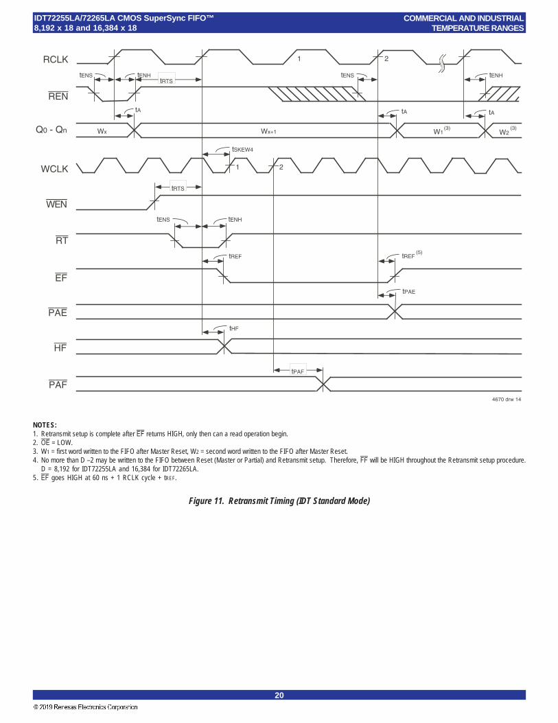
NOTES:1. Retransmit setup is complete after EF returns HIGH, only then can a read operation begin.2. OE = LOW.3. W1 = first word written to the FIFO after Master Reset, W2 = second word written to the FIFO after Master Reset.4. No more than D –2 may be written to the FIFO between Reset (Master or Partial) and Retransmit setup. Therefore, FF will be HIGH throughout the Retransmit setup procedure.
D = 8,192 for IDT72255LA and 16,384 for IDT72265LA.5. EF goes HIGH at 60 ns + 1 RCLK cycle + tREF.
Figure 11. Retransmit Timing (IDT Standard Mode)
tREF
tRTS
tENH
4670 drw 14
tA
tENS
Wx
WCLK
RCLK
REN
RT
EF
PAF
HF
PAE
Q0 - Qn
tSKEW4
1 2
1
W1
tPAF
tHF
tPAE
tREF
Wx+1
2
W2
tENH
WEN
tENS
tRTStENS tENH
(3)
tA tA
(3)
(5)

21
IDT72255LA/72265LA CMOS SuperSync FIFO™8,192 x 18 and 16,384 x 18
COMMERCIAL AND INDUSTRIALTEMPERATURE RANGES
NOTES:1. Retransmit setup is complete after OR returns LOW.2. No more than D –2 words may be written to the FIFO between Reset (Master or Partial) and Retransmit setup. Therefore, IR will be LOW throughout the Retransmit setup
procedure. D = 8,193 for the IDT72255LA and 16,385 for the IDT72265LA.3. OE = LOW4. W1, W2, W3 = first, second and third words written to the FIFO after Master Reset.5. OR goes LOW at 60 ns + 2 RCLK cycles + tREF.
Figure 12. Retransmit Timing (FWFT Mode)
Figure 13. Serial Loading of Programmable Flag Registers (IDT Standard and FWFT Modes)
tREF
tRTS
tENH
4670 drw15
tENS
Wx
WCLK
RCLK
REN
RT
OR
PAF
HF
PAE
Q0 - Qn
tSKEW4
1 2
1
tPAF
tHF
tPAE
tREF
Wx+1
2
W2
tENHtRTS
WENtENS
W1
tENH
(4)
(5)
3 4tENH
W3
tAtA
NOTE:1. X = 12 for the IDT72255LA and X = 13 for the IDT72265LA.
WCLK
SI4670 drw 16
tENHtENS
tLDS
tDS
BIT 0
EMPTY OFFSET
BIT X BIT 0
FULL OFFSET
(1)
tENH
BIT X(1)
tLDHtLDH
tDH
22
IDT72255LA/72265LA CMOS SuperSync FIFO™8,192 x 18 and 16,384 x 18
COMMERCIAL AND INDUSTRIALTEMPERATURE RANGES
NOTES:1. m = PAF offset.2. D = maximum FIFO depth.
In IDT Standard mode: D = 8,192 for the IDT72255LA and 16,384 for the IDT72265LA.In FWFT mode: D = 8,193 for the IDT72255LA and 16,385 for the IDT72265LA.
3. tSKEW2 is the minimum time between a rising RCLK edge and a rising WCLK edge to guarantee that PAF will go HIGH (after one WCLK cycle plus tPAF). If the time between therising edge of RCLK and the rising edge of WCLK is less than tSKEW2, then the PAF deassertion time may be delayed one extra WCLK cycle.
4. PAF is asserted and updated on the rising edge of WCLK only.
Figure 16. Programmable Almost-Full Flag Timing (IDT Standard and FWFT Modes)
WCLKtENH
tCLKH tCLKL
RCLK
(3)
tPAF
4670 drw 19
tENS tENH
tENS
D - (m+1) words in FIFO(2)
tPAF
D - m words in FIFO(2)
tSKEW2
1 2 1 2
D-(m+1) wordsin FIFO(2)
RCLK
Q0 - Q15
tLDHtLDS
tENS
DATA IN OUTPUTREGISTER
PAEOFFSET
PAFOFFSET
tENHtENH
tLDH
4670 drw 18
tCLK
tA tA
tCLKH tCLKL
NOTE:1. OE = LOW
Figure 15. Parallel Read of Programmable Flag Registers (IDT Standard and FWFT Modes)
WCLK
D0 - D15
4670 drw 17
tLDS
tENS
PAEOFFSET
PAFOFFSET
tDS tDH
tLDH
tENH
tCLK
tLDH
tENH
tDH
tCLKH tCLKL
Figure 14. Parallel Loading of Programmable Flag Registers (IDT Standard and FWFT Modes)

23
IDT72255LA/72265LA CMOS SuperSync FIFO™8,192 x 18 and 16,384 x 18
COMMERCIAL AND INDUSTRIALTEMPERATURE RANGES
NOTES:1. For IDT Standard mode: D = maximum FIFO depth. D = 8,192 for the IDT72255LA and 16,384 for the IDT72265LA.2. For FWFT mode: D = maximum FIFO depth. D = 8,193 for the IDT72255LA and 16,385 for the IDT72265LA.
NOTES:1. n = PAE offset.2. For IDT Standard mode3. For FWFT mode.4. tSKEW2 is the minimum time between a rising WCLK edge and a rising RCLK edge to guarantee that PAE will go HIGH (after one RCLK cycle plus tPAE). If the time between
the rising edge of WCLK and the rising edge of RCLK is less than tSKEW2, then the PAE deassertion may be delayed one extra RCLK cycle.5. PAE is asserted and updated on the rising edge of WCLK only.
Figure 18. Half-Full Flag Timing (IDT Standard and FWFT Modes)
WCLKtENH
tCLKH tCLKL
RCLK
tENS
n words in FIFO (2),n+1 words in FIFO (3)
tPAEtSKEW2 tPAE
1 2 1 2
(4)
4670 drw 20
tENS tENH
n+1 words in FIFO (2),n+2 words in FIFO (3)
n words in FIFO (2),n+1 words in FIFO (3)
WCLK
tENS tENH
tENS
tHF
RCLK
tHF
4670 drw 21
tCLKLtCLKH
D/2 words in FIFO(1),
[ + 1] words in FIFO(2)
D/2 + 1 words in FIFO(1),
[ + 2] words in FIFO(2) D/2 words in FIFO(1),
[ + 1] words in FIFO(2)
Figure 17. Programmable Almost-Empty Flag Timing (IDT Standard and FWFT Modes)
24
IDT72255LA/72265LA CMOS SuperSync FIFO™8,192 x 18 and 16,384 x 18
COMMERCIAL AND INDUSTRIALTEMPERATURE RANGES
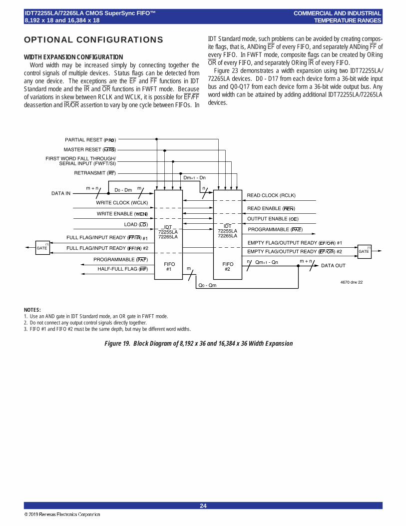
NOTES:1. Use an AND gate in IDT Standard mode, an OR gate in FWFT mode.2. Do not connect any output control signals directly together.3. FIFO #1 and FIFO #2 must be the same depth, but may be different word widths.
OPTIONAL CONFIGURATIONS
WIDTH EXPANSION CONFIGURATIONWord width may be increased simply by connecting together the
control signals of multiple devices. Status flags can be detected fromany one device. The exceptions are the EF and FF functions in IDTStandard mode and the IR and OR functions in FWFT mode. Becauseof variations in skew between RCLK and WCLK, it is possible for EF/FFdeassertion and IR/OR assertion to vary by one cycle between FIFOs. In
Figure 19. Block Diagram of 8,192 x 36 and 16,384 x 36 Width Expansion
IDT Standard mode, such problems can be avoided by creating compos-ite flags, that is, ANDing EF of every FIFO, and separately ANDing FF ofevery FIFO. In FWFT mode, composite flags can be created by ORingOR of every FIFO, and separately ORing IR of every FIFO.
Figure 23 demonstrates a width expansion using two IDT72255LA/72265LA devices. D0 - D17 from each device form a 36-bit wide inputbus and Q0-Q17 from each device form a 36-bit wide output bus. Anyword width can be attained by adding additional IDT72255LA/72265LAdevices.
WRITE CLOCK (WCLK)
m + n m n
MASTER RESET ( )
READ CLOCK (RCLK)
DATA OUTn m + n
WRITE ENABLE ( )
FULL FLAG/INPUT READY ( / )
PROGRAMMABLE ( )
PROGRAMMABLE ( )
EMPTY FLAG/OUTPUT READY ( / ) #2
OUTPUT ENABLE ( )
READ ENABLE ( )
m
LOAD ( ) IDT72255LA72265LA
EMPTY FLAG/OUTPUT READY ( / ) #1
PARTIAL RESET ( )
IDT72255LA72265LA
4670 drw 22
FULL FLAG/INPUT READY ( / ) #2
HALF-FULL FLAG ( )
FIRST WORD FALL THROUGH/SERIAL INPUT (FWFT/SI)
RETRANSMIT ( )
#1
FIFO#2
GATE(1)GATE
(1)
D0 - DmDATA IN
Dm+1 - Dn
Q0 - Qm
Qm+1 - QnFIFO#1

25
IDT72255LA/72265LA CMOS SuperSync FIFO™8,192 x 18 and 16,384 x 18
COMMERCIAL AND INDUSTRIALTEMPERATURE RANGES
Figure 20. Block Diagram of 16,384 x 18 and 32,768 x 18 Depth Expansion
DEPTH EXPANSION CONFIGURATION (FWFT MODE ONLY)The IDT72255LA can easily be adapted to applications requiring depths
greater than 8,192 and 16,384 for the IDT72265LA with an 18-bit buswidth. In FWFT mode, the FIFOs can be connected in series (the dataoutputs of one FIFO connected to the data inputs of the next) with noexternal logic necessary. The resulting configuration provides a totaldepth equivalent to the sum of the depths associated with each singleFIFO. Figure 24 shows a depth expansion using two IDT72255LA/72265LAdevices.
Care should be taken to select FWFT mode during Master Reset for allFIFOs in the depth expansion configuration. The first word written to anempty configuration will pass from one FIFO to the next ("ripple down")until it finally appears at the outputs of the last FIFO in the chain–no readoperation is necessary but the RCLK of each FIFO must be free-running.Each time the data word appears at the outputs of one FIFO, that device'sOR line goes LOW, enabling a write to the next FIFO in line.
For an empty expansion configuration, the amount of time it takes for ORof the last FIFO in the chain to go LOW (i.e. valid data to appear on the lastFIFO's outputs) after a word has been written to the first FIFO is the sum ofthe delays for each individual FIFO:
(N – 1)*(4*transfer clock) + 3*TRCLK
where N is the number of FIFOs in the expansion and TRCLK is theRCLK period. Note that extra cycles should be added for the possibility
that the tSKEW3 specification is not met between WCLK and transfer clock,or RCLK and transfer clock, for the OR flag.
The "ripple down" delay is only noticeable for the first word written to anempty depth expansion configuration. There will be no delay evident forsubsequent words written to the configuration.
The first free location created by reading from a full depth expansionconfiguration will "bubble up" from the last FIFO to the previous one until itfinally moves into the first FIFO of the chain. Each time a free location iscreated in one FIFO of the chain, that FIFO's IR line goes LOW, enablingthe preceding FIFO to write a word to fill it.
For a full expansion configuration, the amount of time it takes for IR of thefirst FIFO in the chain to go LOW after a word has been read from the lastFIFO is the sum of the delays for each individual FIFO:
(N – 1)*(3*transfer clock) + 2 TWCLK
where N is the number of FIFOs in the expansion and TWCLK is theWCLK period. Note that extra cycles should be added for the possibilitythat the tSKEW1 specification is not met between RCLK and transfer clock,or WCLK and transfer clock, for the IR flag.
The Transfer Clock line should be tied to either WCLK or RCLK, which-ever is faster. Both these actions result in data moving, as quickly aspossible, to the end of the chain and free locations to the beginning of thechain.
•
Dn
INPUT READY
WRITE ENABLE
WRITE CLOCK WCLK
DATA IN
RCLKREAD CLOCK
RCLK
OUTPUT ENABLE
OUTPUT READY
QnDn
GND
WCLK
Qn
READ ENABLE
DATA OUT
IDT72255LA72265LA
TRANSFER CLOCK
4670 drw 23
nn n
•
FWFT/SI FWFT/SI
FWFT/SI
IDT72255LA72265LA
26
ORDERING INFORMATIONXXXXX
Device Type X
Power XX
SpeedX
Package X
Process /Temperature
Range
X X
Thin Plastic Quad Flatpack (TQFP, PN64)Slim Thin Quad Flatpack (STQFP, PP64)
Commercial (0°C to +70°C)Industrial (-40°C to +85°C)
Low Power
8,192 x 18 — SuperSync FIFO16,384 x 18 — SuperSync FIFO
4670 drw24
Clock Cycle Time (tCLK)Speed in Nanoseconds
Com'l & Ind'lCom‘l & Ind’l
BLANKI(1)
7225572265
Commercial Only
LA
G(2)
PFTF
101520
Green
TrayTape and Reel
BLANK8
NOTES:1. Industrial temperature range product for 15ns and 20ns speed grades are available as a standard device.2. Green parts are available. For specific speeds and packages contact your local sales office.
LEAD FINISH (SnPb) parts are in EOL process. Product Discontinuation Notice - PDN# SP-17-02
DATASHEET DOCUMENT HISTORY04/25/2001 pgs. 1, 5, 6 and 26.10/17/2005 pgs. 1, 6, 20, 21 and 26. PCN#F0509-01.01/13/2009 pg. 26.07/15/2014 pg. 1, 2 and 26.11/27/2017 Product Discontinuation Notice - PDN# SP-17-02
Last time buy expires June 15, 2018.

27
5 VOLT CMOS SuperSync FIFO™
8,192 x 1816,384 x 18
IDT72255LAIDT72265LAADDENDUM
DIFFERENCES BETWEEN THE IDT72255LA/72265LA AND IDT72255L/72265L
IDT has improved the performance of the IDT72255/72265 SuperSync™ FIFOs. The new versions are designated by the “LA” mark. The LA part is pin-for-pin compatible with the original “L” version. Some difference exist between the two versions. The following table details these differences.
Item NEW PART OLD PART CommentsIDT72255LA IDT72255LIDT72265LA IDT72265L
Pin #3 DC (Don’t Care) - There is FS (Frequency Select) In the LA part this pin must be tiedno restriction on WCLK and to either VCC or GND and mustRCLK. See note 1. not toggle after reset.
First Word Latency 60ns(2) + tREF + 1 TRCLK(4) tFWL1 = 10*Tf(3) + 2TRCLK(4)(ns) First word latency in the LA part is(IDT Standard Mode) a fixed value, independent of the
frequency of RCLK or WCLK.First Word Latency 60ns(2) + tREF + 2 TRCLK(4) tFWL2 = 10*Tf(3) + 3TRCLK(4)(ns) First word latency in the LA part is(FWFT Mode) a fixed value, independent of the
frequency of RCLK or WCLK.Retransmit Latency 60ns(2) + tREF + 1 TRCLK(4) tRTF1 = 14*Tf(3) + 3TRCLK(4)(ns) Retransmit latency in the LA part is(IDT Standard Mode) a fixed value, independent of the
frequency of RCLK or WCLK.Retransmit Latency 60ns(2) + tREF + 2 TRCLK(4) tRTF2 = 14*Tf(3) + 4TRCLK(4)(ns) Retransmit latency in the LA part is
(FWFT Mode) a fixed value, independent of thefrequency of RCLK or WCLK.
ICC1 80mA 180mA Active supply currentICC2 20mA 15mA Standby currentTypical ICC1(5) 15 + 2.1*fS + 0.02*CL*fS(mA) Not Given Typical ICC1 Current calculation
NOTES:1. WCLK and RCLK can vary independently and can be stopped. There is no restriction on operating WCLK and RCLK.2. This is tSKEW3.3. Tf is the period of the ‘selected clock’.4. TRCLK is the cycle period of the read clock.5. Typical ICC1 is based on VCC = 5V, tA = 25°C, fS = WCLK frequency = RCLK frequency (in MHz using TTL levels), data switching at fS/2, CL = Capacitive Load (in pF).
©2017 Integrated Device Technology, Inc. All rights reserved. Product specifications subject to change without notice.
IDT and the IDT logo are registered trademarks of Integrated Device Technology, Inc and the SuperSyncFIFO is a trademark of Integrated Device Technology, Inc.
COMMERCIAL AND INDUSTRIAL TEMPERATURE RANGES

Corporate HeadquartersTOYOSU FORESIA, 3-2-24 Toyosu,Koto-ku, Tokyo 135-0061, Japanwww.renesas.com
Contact InformationFor further information on a product, technology, the most up-to-date version of a document, or your nearest sales office, please visit:www.renesas.com/contact/
TrademarksRenesas and the Renesas logo are trademarks of Renesas Electronics Corporation. All trademarks and registered trademarks are the property of their respective owners.
IMPORTANT NOTICE AND DISCLAIMER
RENESAS ELECTRONICS CORPORATION AND ITS SUBSIDIARIES (“RENESAS”) PROVIDES TECHNICAL SPECIFICATIONS AND RELIABILITY DATA (INCLUDING DATASHEETS), DESIGN RESOURCES (INCLUDING REFERENCE DESIGNS), APPLICATION OR OTHER DESIGN ADVICE, WEB TOOLS, SAFETY INFORMATION, AND OTHER RESOURCES “AS IS” AND WITH ALL FAULTS, AND DISCLAIMS ALL WARRANTIES, EXPRESS OR IMPLIED, INCLUDING, WITHOUT LIMITATION, ANY IMPLIED WARRANTIES OF MERCHANTABILITY, FITNESS FOR A PARTICULAR PURPOSE, OR NON-INFRINGEMENT OF THIRD PARTY INTELLECTUAL PROPERTY RIGHTS.
These resources are intended for developers skilled in the art designing with Renesas products. You are solely responsible for (1) selecting the appropriate products for your application, (2) designing, validating, and testing your application, and (3) ensuring your application meets applicable standards, and any other safety, security, or other requirements. These resources are subject to change without notice. Renesas grants you permission to use these resources only for development of an application that uses Renesas products. Other reproduction or use of these resources is strictly prohibited. No license is granted to any other Renesas intellectual property or to any third party intellectual property. Renesas disclaims responsibility for, and you will fully indemnify Renesas and its representatives against, any claims, damages, costs, losses, or liabilities arising out of your use of these resources. Renesas' products are provided only subject to Renesas' Terms and Conditions of Sale or other applicable terms agreed to in writing. No use of any Renesas resources expands or otherwise alters any applicable warranties or warranty disclaimers for these products.
(Rev.1.0 Mar 2020)
© 2020 Renesas Electronics Corporation. All rights reserved.


![AT25128B and AT25256B · AT25128B/256B [DATASHEET] 3 Atmel-8698E-SEEPROM-AT25128B-256B-Datasheet_012015 3. Block Diagram Figure 3-1. Block Diagram Memory Array 16,384/32,768 x 8 Status](https://img.pdfslide.us/doc/110x75/609cce59f0b0c86cf830d03c/at25128b-and-at25256b-at25128b256b-datasheet-3-atmel-8698e-seeprom-at25128b-256b-datasheet012015.jpg)