Embed Size (px)
Citation preview
Mattausch, CMOS Design, H20/6/6 1
Arithmetic Modules (Part 1)
• Digital Processing Systems• Base-2 Numbers (Binaries) • Circuits for Addition and Subtraction
– Adders for Single-Bit Binaries– Combinational Adders/Subtractors for Multi-Bit Binaries – Sequential Adders/Subtractors for Multi-Bit Binaries
• Circuits for Data Shifting
CMOS Logic Circuit Designhttp://www.rcns.hiroshima-u.ac.jp
Link(リンク): センター教官講義ノート の下 CMOS論理回路設計

Mattausch, CMOS Design, H20/6/6 2
Digital Processing Systems- Basic Structure- Construction of the Datapath
(Arithmetic Part)
Mattausch, CMOS Design, H20/6/6 3
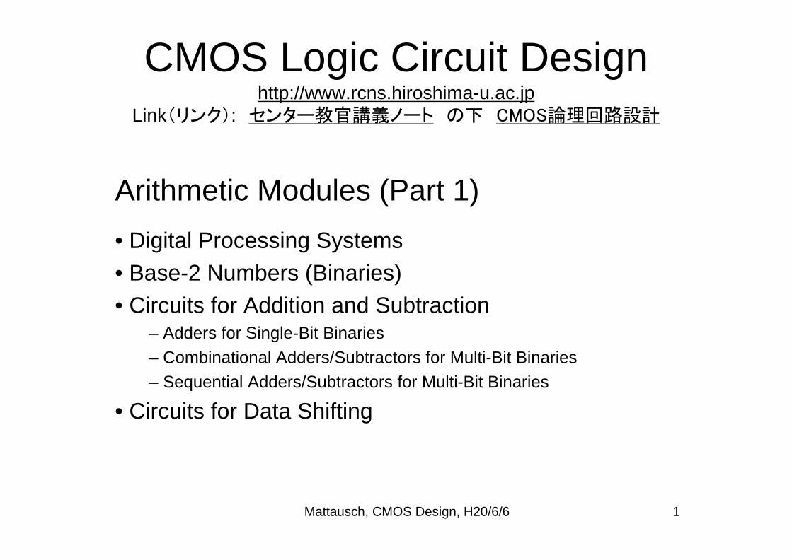
Basic Digital-Processing-System Structure
The datapath in a digital processing system is the system unit, which carries out the actual data-processing functions.
Input/Output Control
Memory
Datapath
InterconnectUnit
Memory:SRAM, ROM, DRAM
Control:Finite-State Machine, Micro-Program
Input/Output:Buffer, A/D-, D/A-Converter, Protection Circuits
Interconnect Unit:Busses, Switches, Arbiters
Datapath:Adder, Multiplier, Shifter, Logic Unit, etc.
Mattausch, CMOS Design, H20/6/6 4
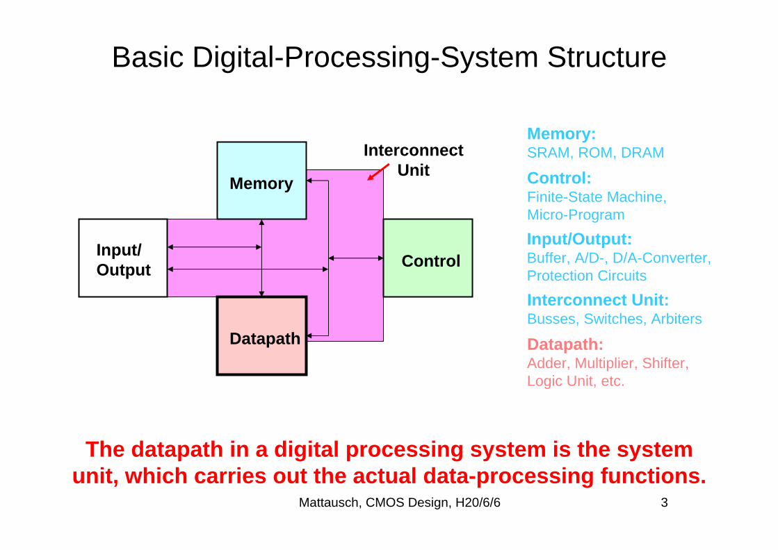
Construction of the Datapath (Arithmetic Part)
A datapath consists of registers, arithmetic units and a multiplexer for current-operation selection.
Control
Reg
iste
r
Ad
der
Sh
ifte
r
Bo
ole
an U
nit
Mu
ltip
lier
Mu
ltip
lexe
r
Bit 0Bit 1Bit 2Bit 3
Bit 30Bit 31
Dat
a-In
Dat
a-O
ut
Today’s Lecture
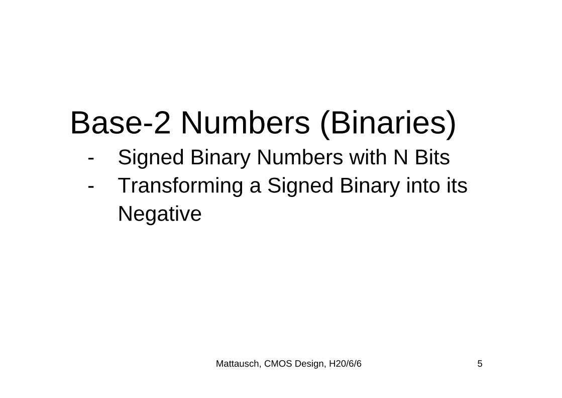
Mattausch, CMOS Design, H20/6/6 5
Base-2 Numbers (Binaries)- Signed Binary Numbers with N Bits - Transforming a Signed Binary into its
Negative
Mattausch, CMOS Design, H20/6/6 6
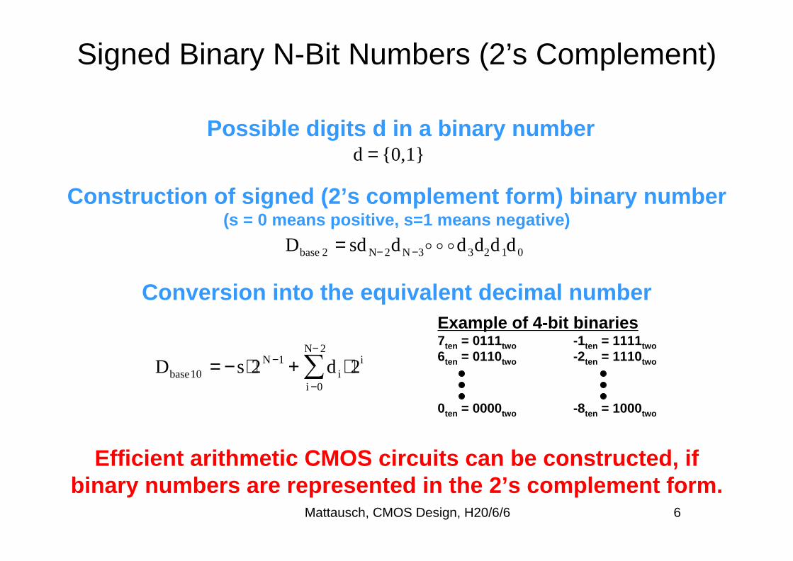
Signed Binary N-Bit Numbers (2’s Complement)
Efficient arithmetic CMOS circuits can be constructed, if binary numbers are represented in the 2’s complement form.
Possible digits d in a binary numberd = {0,1}
Construction of signed (2’s complement form) binary number (s = 0 means positive, s=1 means negative)
Dbase 2 = sd N−2dN −3o o od3d2d1d0
Conversion into the equivalent decimal number
Dbase10 = −s⋅2N −1 + di ⋅ 2i
i −0
N−2
∑
Example of 4-bit binaries7ten = 0111two -1ten = 1111two6ten = 0110two -2ten = 1110two
0ten = 0000two -8ten = 1000two

Mattausch, CMOS Design, H20/6/6 7
Negative of a 2’s Complement Binary
Above method of calculating the negative of a binary is often exploited for simplifying arithmetic hardware.
For every D following equation must be valid(The result of adding the inverted bits and non-inverted bits of any binary consists
of only 1s at all its digits. Thus this result is the representation of -1)
D+ D = −1
Consequently, the negative of any 2’s complement binary can be calculated by inverting all bits and adding a 1 afterwards.
− D = D +1

Mattausch, CMOS Design, H20/6/6 8
Circuits for Addition and Subtraction
- Adders for Single-Bit Binaries - Combinational Adders/Subtractors for
Multi-Bit Binaries- Sequential Adders/Subtractors for
Multi-Bit Binaries

Mattausch, CMOS Design, H20/6/6 9
Binary-Adder Principle, 1-Bit-Adder Truth-Table
The basic circuit for realizing the adder arithmetic is the fulladder, a combinational circuit with 3 inputs and 2 outputs.
Process of adding two binariesleads to a 1-bit adder unit with
3 inputs and 2 output
1-bit full-adder truth-table
FullAdder
A B
Cin Cout
SA B Cin S Cout Carry
Status
0 0 0 0 0 delete
0 0 1 1 0 delete
0 1 0 1 0 propagate
0 1 1 0 1 propagate
1 0 0 1 0 propagate
1 0 1 0 1 propagate
1 1 0 0 1 generate
1 1 1 1 1 generate
1
+B:
A:
C:
0
11
110
000
0 0
1(0)0(1)1(1)1(0)0(0)0(0)
(0)(1)(1)(0)(0)(Carry Bits)
Basic Adder Unit(Full Adder)
Mattausch, CMOS Design, H20/6/6 10
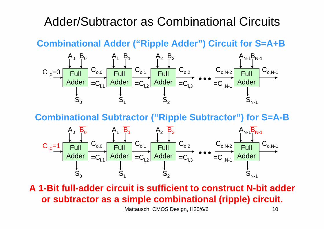
Adder/Subtractor as Combinational Circuits
A 1-Bit full-adder circuit is sufficient to construct N-bit adder or subtractor as a simple combinational (ripple) circuit.
Combinational Adder (“Ripple Adder”) Circuit for S=A+B
Ci,0=0 FullAdder
A0 B0
Co,0
S0
=Ci,1
FullAdder
A1 B1
Co,1
S1
=Ci,2
FullAdder
A2 B2
Co,2
S2
=Ci,3
FullAdder
AN-1BN-1
Co,N-1
SN-1
Co,N-2
=Ci,N-1
Combinational Subtractor (“Ripple Subtractor”) for S=A-B
Ci,0=1 FullAdder
A0 B0
Co,0
S0
=Ci,1
FullAdder
A1 B1
Co,1
S1
=Ci,2
FullAdder
A2 B2
Co,2
S2
=Ci,3
FullAdder
AN-1BN-1
Co,N-1
SN-1
Co,N-2
=Ci,N-1
Mattausch, CMOS Design, H20/6/6 11
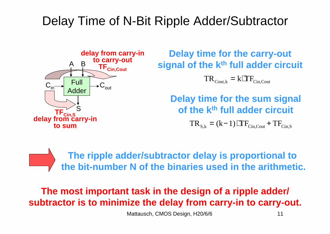
Delay Time of N-Bit Ripple Adder/Subtractor
The most important task in the design of a ripple adder/ subtractor is to minimize the delay from carry-in to carry-out.
Delay time for the carry-out signal of the kth full adder circuit
TRCout,k = k⋅ TFCin,Cout
The ripple adder/subtractor delay is proportional to the bit-number N of the binaries used in the arithmetic.
Delay time for the sum signal of the kth full adder circuit
TRS,k = (k−1) ⋅ TFCin,Cout + TFCin,S
FullAdder
A B
Cin Cout
S
delay from carry-in to carry-out
TFCin,Cout
TFCin,Sdelay from carry-in
to sum
Mattausch, CMOS Design, H20/6/6 12
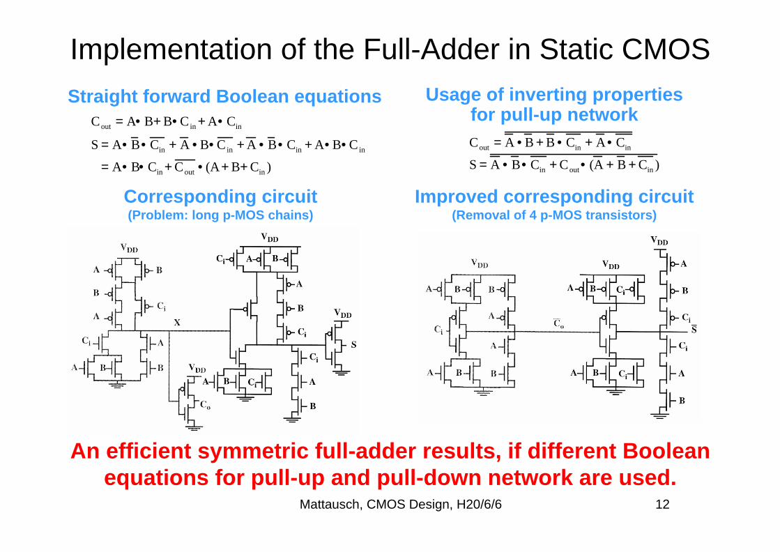
Implementation of the Full-Adder in Static CMOS
An efficient symmetric full-adder results, if different Boolean equations for pull-up and pull-down network are used.
Straight forward Boolean equations
S = A• B• Cin + A • B• Cin + A • B• Cin + A• B• Cin
= A• B• Cin + Cout • (A+ B+ Cin )
Cout = A• B+ B• Cin + A• Cin
Corresponding circuit(Problem: long p-MOS chains)
Usage of inverting properties for pull-up network
S = A • B• Cin + Cout• (A + B + Cin )
Cout = A • B + B • Cin + A • Cin
Improved corresponding circuit(Removal of 4 p-MOS transistors)
Mattausch, CMOS Design, H20/6/6 13
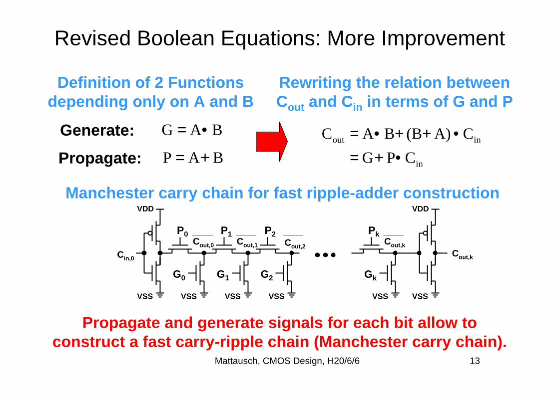
Revised Boolean Equations: More Improvement
Propagate and generate signals for each bit allow to construct a fast carry-ripple chain (Manchester carry chain).
Definition of 2 Functions depending only on A and B
Manchester carry chain for fast ripple-adder construction
BAG •=
BAP +=
Generate:
Propagate: in
inout
CPG
CA)(BBAC
•+=•++•=
Rewriting the relation between Cout and Cin in terms of G and P
VDD
VSS VSS
P0
G0
Cin,0
Cout,0
VSS
P1
G1
Cout,1
VSS
P2
G2
Cout,2
VSS
Pk
Gk
Cout,k
VDD
VSS
Cout,k
Mattausch, CMOS Design, H20/6/6 14
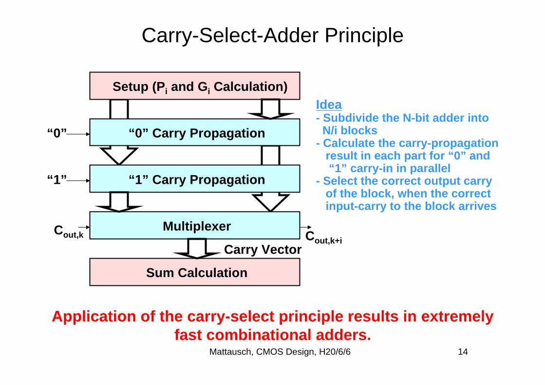
Carry-Select-Adder Principle
Application of the carry-select principle results in extremely fast combinational adders.
Idea- Subdivide the N-bit adder intoN/i blocks
- Calculate the carry-propagationresult in each part for “0” and“1” carry-in in parallel
- Select the correct output carryof the block, when the correctinput-carry to the block arrives
Setup (Pi and Gi Calculation)
“0” Carry Propagation
“1” Carry Propagation
Multiplexer
Sum Calculation
“0”
“1”
Cout,k
Carry VectorCout,k+i
Mattausch, CMOS Design, H20/6/6 15
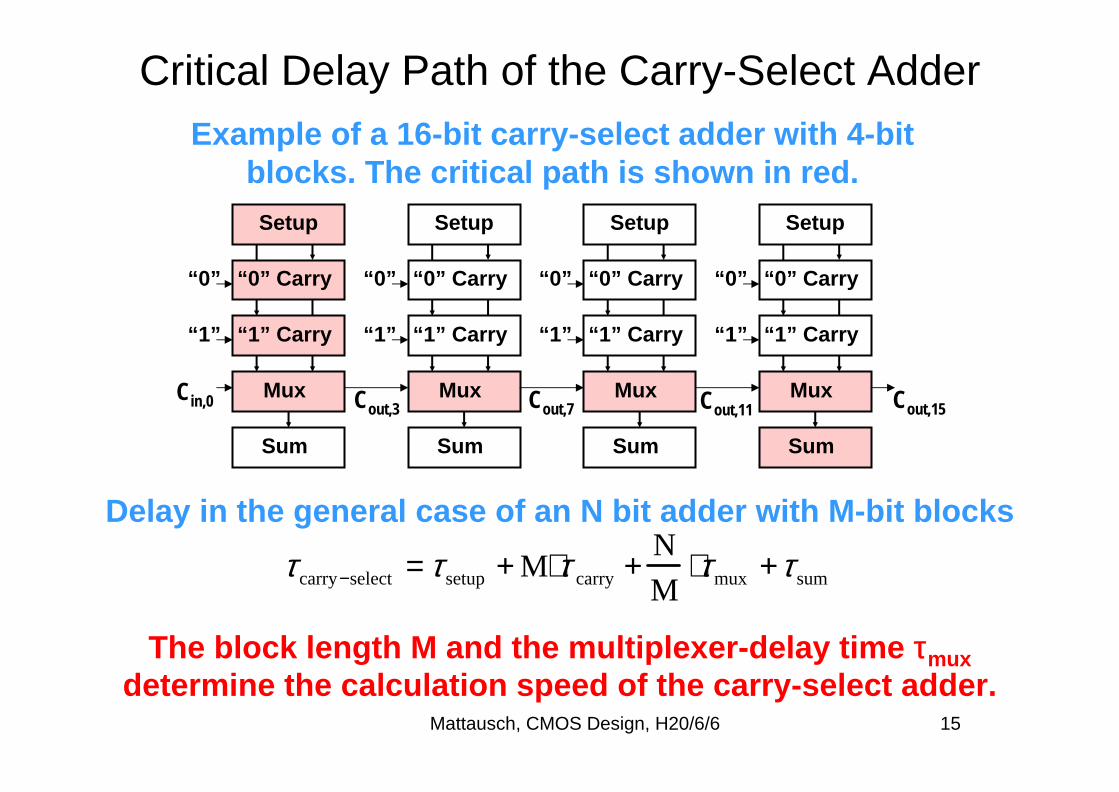
Critical Delay Path of the Carry-Select Adder
The block length M and the multiplexer-delay time τmuxdetermine the calculation speed of the carry-select adder.
Cout,7
Setup
“0” Carry“0”
“1”
Cin,0
“1” Carry
Mux
Sum
Setup
“0” Carry
“1” Carry
Mux
Sum
“0”
“1”
Cout,3
Setup
“0” Carry
“1” Carry
Mux
Sum
“0”
“1”
Setup
“0” Carry
“1” Carry
Mux
Sum
“0”
“1”
Cout,11 Cout,15
Example of a 16-bit carry-select adder with 4-bit blocks. The critical path is shown in red.
τ carry−select = τ setup + M⋅τ carry +N
M⋅τmux +τ sum
Delay in the general case of an N bit adder with M-bit blocks
Mattausch, CMOS Design, H20/6/6 16
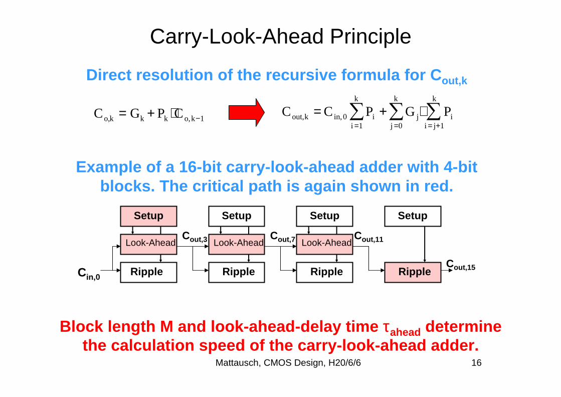
Carry-Look-Ahead Principle
Block length M and look-ahead-delay time τahead determine the calculation speed of the carry-look-ahead adder.
Direct resolution of the recursive formula for Cout,k
Example of a 16-bit carry-look-ahead adder with 4-bit blocks. The critical path is again shown in red.
Co,k = Gk + Pk ⋅Co,k−1Cout,k = Cin,0 Pi
i =1
k
∑ + G j⋅ Pii = j+1
k
∑j =0
k
∑
Setup
Cin,0
Look-Ahead
Ripple
Setup
Cout,3
Setup Setup
Cout,7 Cout,11
Ripple Ripple Ripple
Look-Ahead Look-Ahead
Cout,15

Mattausch, CMOS Design, H20/6/6 17
Circuits for Addition and Subtraction
- Adders for Single-Bit Binaries - Combinational Adders/Subtractors for
Multi-Bit Binaries- Sequential Adders/Subtractors for
Multi-Bit Binaries
Mattausch, CMOS Design, H20/6/6 18
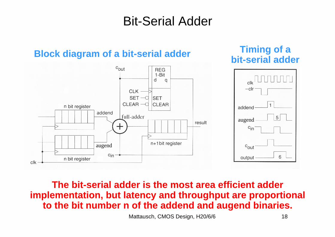
Bit-Serial Adder
The bit-serial adder is the most area efficient adder implementation, but latency and throughput are proportional
to the bit number n of the addend and augend binaries.
Block diagram of a bit-serial adder
augend
augend
Timing of a bit-serial adder
Mattausch, CMOS Design, H20/6/6 19
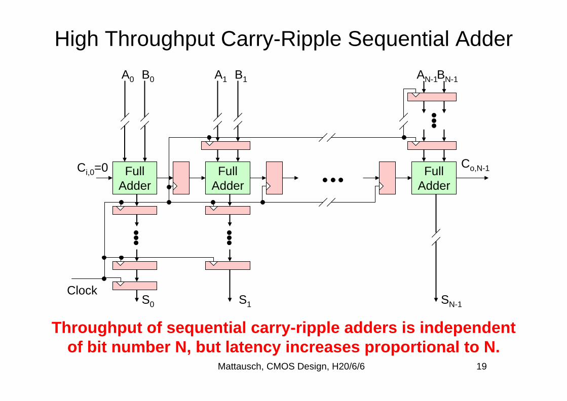
High Throughput Carry-Ripple Sequential Adder
Throughput of sequential carry-ripple adders is independent of bit number N, but latency increases proportional to N.
Ci,0=0 FullAdder
A0 B0
S0
FullAdder
A1 B1
S1
FullAdder
AN-1BN-1
Co,N-1
SN-1
Clock
Mattausch, CMOS Design, H20/6/6 20
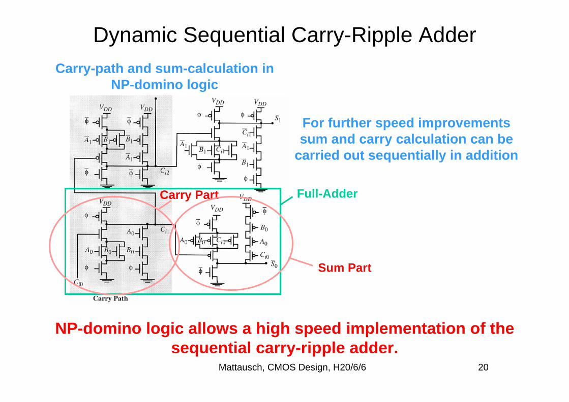
Dynamic Sequential Carry-Ripple Adder
NP-domino logic allows a high speed implementation of the sequential carry-ripple adder.
Carry-path and sum-calculation inNP-domino logic
Corresponding circuit(Problem: long p-MOS chains)
For further speed improvementssum and carry calculation can be
carried out sequentially in addition
Full-AdderCarry Part
Sum Part
Mattausch, CMOS Design, H20/6/6 21
Circuits for Data Shifting
Mattausch, CMOS Design, H20/6/6 22
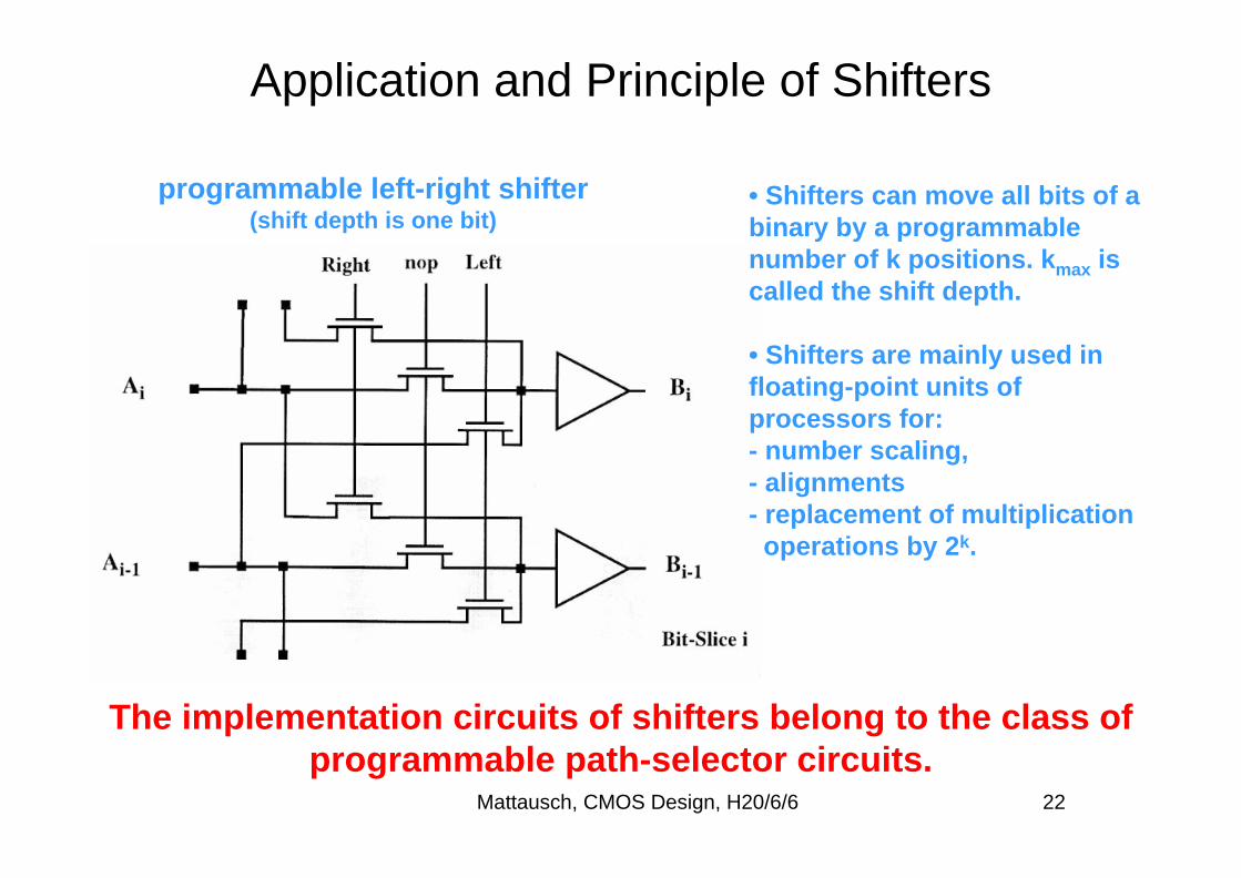
Application and Principle of Shifters
The implementation circuits of shifters belong to the class of programmable path-selector circuits.
programmable left-right shifter(shift depth is one bit)
• Shifters can move all bits of a binary by a programmable number of k positions. kmax is called the shift depth.
• Shifters are mainly used in floating-point units of processors for: - number scaling, - alignments - replacement of multiplicationoperations by 2k.

Mattausch, CMOS Design, H20/6/6 23
Logarithmic Shifters
Logarithmic shifting leads to very effective shifter circuits.
programmable logarithmic shifter(shift depth is 0-7 bit)
Logarithmic shifters use stages which can shift by powers of 2.
Therefore, the bits of the binary which determines the shift-length can be directly used as the control signals of the logarithmic shifter.


![Area and Power Efficient CMOS Adder Design by Hybridizing ... · Fig 1: 20T Transmission Gate based Full Adder [14] Full adder design by using 20 and 16 transistors has been proposed](https://img.pdfslide.us/doc/110x75/5f2ce51b2e67332184676f6e/area-and-power-efficient-cmos-adder-design-by-hybridizing-fig-1-20t-transmission.jpg)
![Relative Performance Analysis of Different CMOS Full Adder ... · devices [6]. The performance of 1-bit FA has compared using different CMOS logic design styles in [12-14]. The functionality](https://img.pdfslide.us/doc/110x75/5f44fdd4e0bb0f7cca34ea82/relative-performance-analysis-of-different-cmos-full-adder-devices-6-the.jpg)