Embed Size (px)
Citation preview
Mattausch, CMOS Design, H19/6/29 1
Memory Circuits (Part 1)
• Overview of Memory Types• Memory with Address-Based Access
– Principle of Data Access by Address Decoding– Volatile Random Read/Write-Access Memory
– Non-Volatile Random Read-Only Memory– Non-Volatile Random Read/Write-Access Memory
• Memory with Content-Based Access– Principle of Data Access by Content Matching
– Conventional Content-Addressable Memory
CMOS Logic Circuit Designhttp://www.rcns.hiroshima-u.ac.jp
Link(リンク): センター教官講義ノート の下 CMOS論理回路設計

Mattausch, CMOS Design, H19/6/29 2
Overview of the Memory Types
Semiconductor Memory
Address-Based Access Content-Based Access
VolatileStorage
Non-VolatileStorage
DRAM
SRAM
ROM
EEPROM
Read-OnlyAccess
Read/WriteAccess
FlashEEPROM
FRAM MRAM
ExactMatch
BestMatch
TernaryCAM
ConventionalCAM
Distance-MeasureBased CAM
Most widely used: Today in use: Today today under development:

Mattausch, CMOS Design, H19/6/29 3
Memory with Address-Based Access
- Principle of Data Access by Address Decoding• Row Decoding• Column Decoding
- Volatile Random Read/Write-AccessMemory • Static Random Access Memory (SRAM) • Dynamic Random Access Memory (DRAM)
Mattausch, CMOS Design, H19/6/29 4
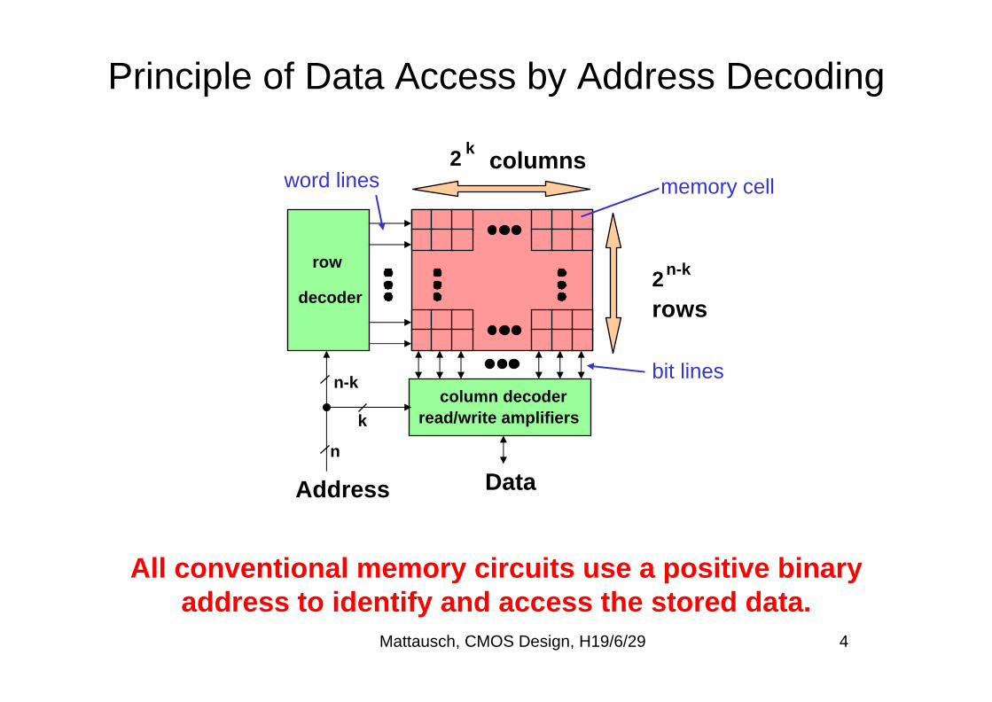
Principle of Data Access by Address Decoding
All conventional memory circuits use a positive binary address to identify and access the stored data.
row
decoder
column decoderread/write amplifiers
Address
n
n-k
k
Data
2n-k
rows
2 kcolumns
memory cellword lines
bit lines

Mattausch, CMOS Design, H19/6/29 5
Single Stage Row Decoder
The row-decoder has to activate exactly one row for each row address. With an n-bit address 1 of 2n rows is selectable.
AND-decoder for 2 address bits 2-input AND circuit
VDD
VSS
PMOS-transistor
NMOS-transistor

Mattausch, CMOS Design, H19/6/29 6
Two Stage Row Decoder
Pre-decoding in a first decoder stage keeps the AND-gate fan-in small. Shorter delay times result.
2-stage row-decoder circuitfor
a 3-bit address
Pre-decodeStage
Final Row-Decode Stage

Mattausch, CMOS Design, H19/6/29 7
Inverted Selected Data
Normal Selected Data to
Sense Amplifier
Tree Column Decoder (Example SRAM)
The column decoder connects the selected data column to the sense amplifier. The tree decoder has the best area
efficiency but a large delay for many column-address bits.
Mattausch, CMOS Design, H19/6/29 8
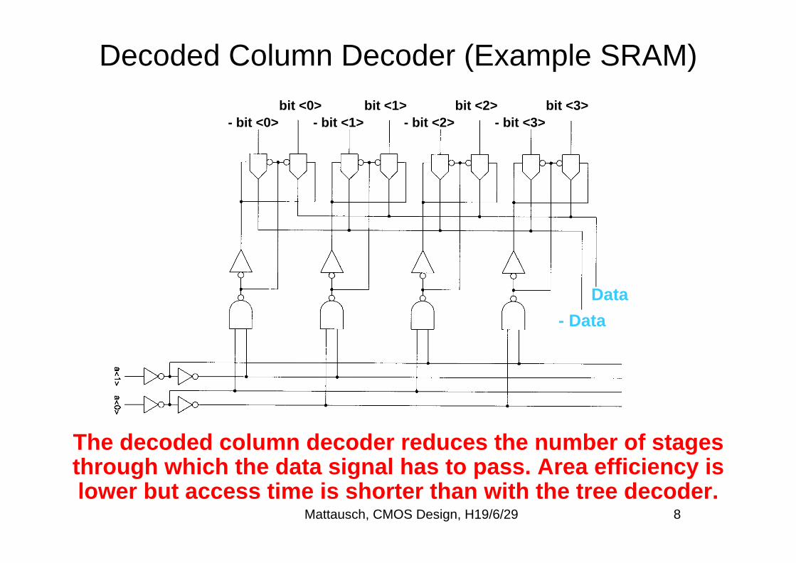
bit <0> - bit <0>
bit <1> - bit <1>
bit <2> - bit <2>
bit <3> - bit <3>
- Data
Data
Decoded Column Decoder (Example SRAM)
The decoded column decoder reduces the number of stages through which the data signal has to pass. Area efficiency is lower but access time is shorter than with the tree decoder.

Mattausch, CMOS Design, H19/6/29 9
Memory with Address-Based Access
- Principle of Data Access by Address Decoding• Row Decoding• Column Decoding
- Volatile Random Read/Write-AccessMemory • Static Random Access Memory (SRAM) • Dynamic Random Access Memory (DRAM)

Mattausch, CMOS Design, H19/6/29 10
Basic SRAM Architecture
The SRAM architecture requires also the elements “RAM cell”, “bit line conditioning”, “sense amplifier” and “write buffers”.
Shown is just
one bit of the
complete SRAM !
Elements Additional
toDecoding

Mattausch, CMOS Design, H19/6/29 11
SRAM Storage Cells
A 6-transistor CMOS SRAM cell has lower power dissipation, but requires larger area than a 4-transistor NMOS SRAM cell.
6 transistor
CMOS SRAM cell
4 transistor
NMOS SRAM cell

Mattausch, CMOS Design, H19/6/29 12
SRAM Read Operation
The SRAM read operation requires a careful combined design of memory cell, bitline conditioning and sense amplifier.
word
static-load bitline
conditioning
data
current mirror sense amplifier
VDD
VSS
Read Operation Circuitry Signal Waveforms (Voltages)and
Critical Circuit Part for Reading
bitline voltage
cell-internalvoltage

Mattausch, CMOS Design, H19/6/29 13
SRAM Write Operation
The SRAM write operation requires enough driving power of the buffer and careful design of transistors N1/N2 and N3/N4.
static-load bitline
conditioning
write buffer and selector
Write Operation Circuitry Signal Waveforms (Voltages)for Writing

Mattausch, CMOS Design, H19/6/29 14
DRAM Storage Cells
Today only the 1 transistor DRAM cell is used in DRAM chips.
4 TransistorNMOS DRAM Cell
3 TransistorNMOS DRAM Cell
2 TransistorNMOS DRAM Cell
(1 Transistor used as Capacitor)
1 Transistor + CapacitorNMOS DRAM Cell
(Free Capacitor Construction Method )

Mattausch, CMOS Design, H19/6/29 15
DRAM Storage Cells
Today the stacked capacitor cell is most widely used.
Stacked Capacitor Cell
InsulatorCapacitor Plate (Poly 2)
Trench Capacitor Cell
InversionLayer
Planar Capacitor Cell
Capacitor Plate (Poly 2)
InversionLayer

Mattausch, CMOS Design, H19/6/29 16
Basic DRAM Architecture
The dynamic memory cell requires a complicated timing generator and periodical refresh of the stored data.
Column-Address Buffer
Address Signals A1-An
Bu
ffer
Ro
w-A
dd
ress
CAS
RAS
Data In
Input Buffer
Write Circuit Multiplexer Sense
Amp.Output Driver
Data Out
Column DecoderR
ow
Dec
od
er
Field of
Memory Cells Timing Generator
A1 - Ak
Ak+1 - An
2k
2n-k
φp, φa
(Row Address Select)
(Column Address Select)

Mattausch, CMOS Design, H19/6/29 17
DRAM Read/Write Circuitry
The DRAM Read/Write circuitry is more
complicated than that of an SRAM.
Dummy storage cells and preamplifiers are
used.
Bitline conditioning
Upper dummystorage cell
Upper and lowerfield of
storage cellLower dummystorage cell
Preamplifier and Multiplexer
Writecircuit
Sense amp and
Output driver

Mattausch, CMOS Design, H19/6/29 18
Memory with Address-Based Access
- Non-Volatile Random Read-Only-AccessMemory• Conventional Read Only Memory (ROM)
- Non-Volatile Random Read/Write-AccessMemory • Electrically Erasable Programmable ROM (EEPROM)

Mattausch, CMOS Design, H19/6/29 19
Single StageRow Decoder
Field of Memory Cells
ROM Structure Example
DecodedColumn Decoder(decode stage)
Conventional ROM Architecture
Data stored in conventional ROMs needs presence/absence of hardware and thus cannot be changed after fabrication.
DecodedColumn Decoder
(select stage)
B
W
= 1
B
W
= 0
Storage Cell
Mattausch, CMOS Design, H19/6/29 20
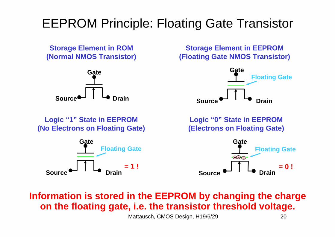
EEPROM Principle: Floating Gate Transistor
Information is stored in the EEPROM by changing the charge on the floating gate, i.e. the transistor threshold voltage.
Gate
Source Drain
Floating Gate
= 1 !
Gate
Source Drain
Floating Gate
= 0 !- - -
Gate
Source Drain
Gate
Source Drain
Floating Gate
Storage Element in ROM(Normal NMOS Transistor)
Storage Element in EEPROM(Floating Gate NMOS Transistor)
Logic “1” State in EEPROM(No Electrons on Floating Gate)
Logic “0” State in EEPROM(Electrons on Floating Gate)

Mattausch, CMOS Design, H19/6/29 21
Programming Method of the Floating Gate
Information storage on the floating gate requires the on-chip generation of a relatively high programming voltage (~ 20V).
Floating Gate(Programming)
Vprog
VSS
Gate
Floating Gate
DrainSource
Bulk p-
n+ n+
Vprog
Gate
Floating Gate
DrainSource
Bulk p-
n+ n+
VSS
Floating Gate(Erasing)

Mattausch, CMOS Design, H19/6/29 22
Memory with Content-Based Access
- Principle of Data Access by ContentMatching
- Conventional Content Addressable Memory (CAM)

Mattausch, CMOS Design, H19/6/29 23
Principle of Memory Access by Content Matching
High content-matching performance requires a parallel distance calculation for all reference data.
Input Data IN={IN1, IN2,…,INW}
Reference Data 1 REF1={REF11, REF12,…, REF1W}
Distance Calculation D1(IN, REF1)Reference Data 2
REF2={REF21, REF22,…, REF2W}Distance Calculation D2(IN, REF2)
Reference Data R REFR={REFR1, REFR2,…, REFRW}
Distance Calculation DR(IN, REFR)
Best Match
Calculation
MIN(D1,…,DR)
Winner ofContent Matching

Mattausch, CMOS Design, H19/6/29 24
Common Distance Measures and Applications
Content-based memory access is an important concept for realizing intelligent systems in the future information society.
Di = IN j− REFijj =1
W
∑
Common Distance Measure
Di is called Hamming distance, ifINj and REFij are 1-bit binaries.
Di is called Manhattan distance, ifINj and REFij are n-bit binaries with n>1.
Important Applications
• Data-base systems with fast dataretrieval.
• Computers with high performancememory hierarchy (e.g. cache andvirtual memory).
• Speech and picture recognition or language translation with code books.
• Intelligent systems with recognitionand learning capability.

Mattausch, CMOS Design, H19/6/29 25
Conventional Content-Addressable Memory
Capabilities of the conventional content-addressable memory (CAM) are very limited, because only Di=0 can be evaluated.
Di = IN j− REFijj =1
W
∑ = 0
ConventionalDistance Measure
Conventional hardware forcontent-addressable memories can only retrieve data withdistance zero to the input.
Conventional CAM Cell
cell- cell 6 TransistorSRAM Cell
EXOR
DistributedNOR
(Pull-Down Transistor)
bit⊗ cell( )
Mattausch, CMOS Design, H19/6/29 26
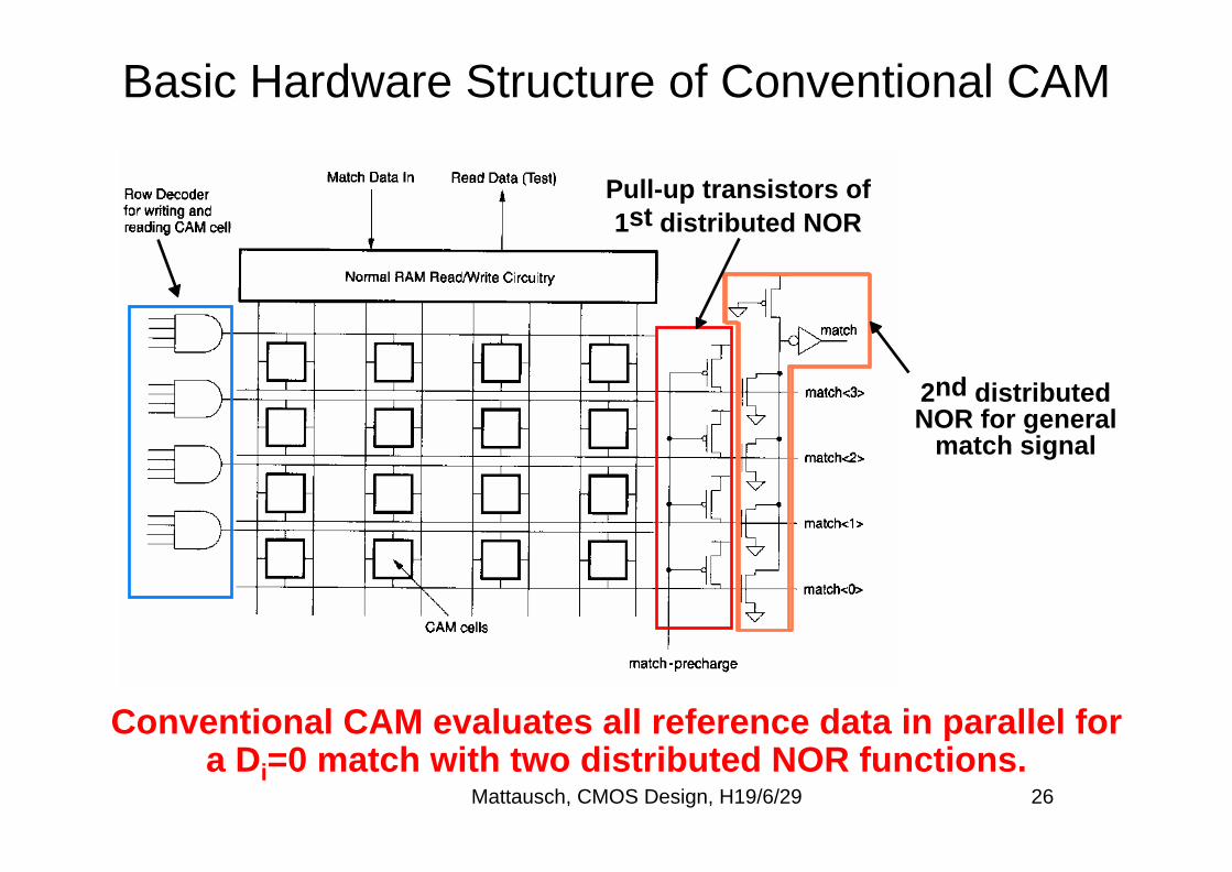
Basic Hardware Structure of Conventional CAM
Conventional CAM evaluates all reference data in parallel for a Di=0 match with two distributed NOR functions.
2nd distributedNOR for general
match signal
Pull-up transistors of1st distributed NOR

Mattausch, CMOS Design, H19/6/29 27
Principle of Data Retrieval with CAM
Conventional CAMs with only Di=0 match capability can be used for fast data retrieval problems, e. g. in internet routers.
CAM Memory Array(N Key Pattern, each m Bit)
RAM Memory Array(N Data Words, each k Bit)
N Match Lines of CAM =RAM Word Lines
Exact Matching of Input Key and Stored Keys
Output of Retrieved Data Word
Input of Search Key