Embed Size (px)
Citation preview

Radiation Hardened 32K x 8 CMOS
EEPROM
IntroductionThe W28C256 is a 32K x 8 radiation hardened EEPROM designed by Sandia National Laboratories, Albuquerque, NM, and manufactured by the Northrop Grumman Advanced Technology Center, Baltimore, MD, using nonvolatile memory technology transferred from Sandia. It is built using a mature dual well CMOS process using N on N+ epitaxial silicon and a two layer interconnect system.
Features• 1.25 Micrometer Radiation Hardened CMOS on
Epi - Total Dose up to 300 Krad (Si) - Transient Logic Upset >5E7 Rad(Si)/sec - Memory Data Loss >1E12 Rad(Si)/sec• Single Event Upsets - SEU During READ LETth = 60 MeV/mg/cm2
- SEU in Address/Data Latches, LETth = 35 MeV/mg/cm2
- Permanent SEU damage (During Write Only), Atomic Number > Kr
• No Latchup• Compatible with commercial EEPROMs• JEDEC pin compatible in center 28 pins• Full military operating temperature range,
screened to specific test methods for commercial, Class B, or modified Hi Rel.
Supports these commercial features: - Self-Timed Programming - Combined Erase/Write - Auto Program Start - +5V only read operation - Asynchronous Addressing - 64 Word Page - Data Polling
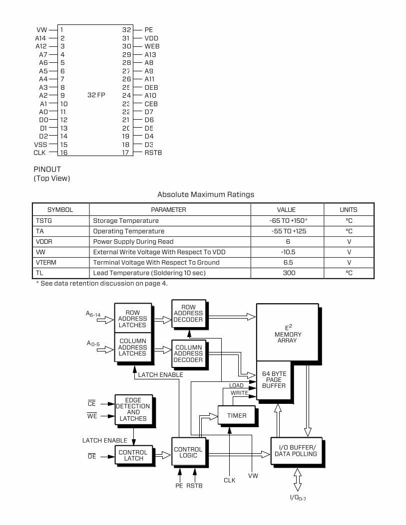
VWA14A12
A7A6A5A4A3A2A1A0D0D1D2
VSSCLK
32313029282726252423222120191817
PEVDDWEBA13A8A9A11OEBA10CEBD7D6D5D4D3RSTB
12345678910111213141516
32 FP
PINOUT(Top View)
Absolute Maximum Ratings
SYMBOL PARAMETER VALUE UNITS
TSTG Storage Temperature -65 TO +150* °C
TA Operating Temperature -55 TO +125 °C
VDDR Power Supply During Read 6 V
VW External Write Voltage With Respect To VDD -10.5 V
VTERM Terminal Voltage With Respect To Ground 6.5 V
TL Lead Temperature (Soldering 10 sec) 300 °C
* See data retention discussion on page 4.
CONTROLLATCH
EDGEDETECTION
ANDLATCHES
ROWADDRESSDECODER
COLUMNADDRESSDECODER
CONTROLLOGIC
TIMER
ROWADDRESSLATCHES
COLUMNADDRESSLATCHES
64 BYTE PAGE
BUFFER
E2
MEMORYARRAY
I/O BUFFER/ DATA POLLING
LATCH ENABLE
CLKVW
RSTBPE
LATCH ENABLE
CE
WE
OE
LOADWRITE
A0-5
A6-14
I/O0-7
DC Operating CharacteristicsTA = -55° to + 125°C, VDD = 5V ±5%, unless otherwise specified
LIMITS
SYMBOL PARAMETER MIN MAX UNITS TEST CONDITIONS
IDDS Static I Read 10 mA Read Mode, DC
IDDR Active I Read 17 mA Read Mode, 2 MHz
IDDW Active I Write 2 mA Write Mode
IW1 Inactive I Write -25 uA Standby or Read (Note 1)
IDDSB Standby I 1.5 mA
IIH Input I High 1 uA
IIL Input I Low 1 uA
IOH Output I High 3 mA VOH = 4.25V
IOL Output I Low -3 mA VOL = 0.5 V
VIL Input V Low -0.5 0.95 V
VIH Input V High 3.8 VDD+0.5
V
VOH Output V High 4.25 V VDD = 4.75 VW = -4.75 VIH = 3.8 VIL = 0.95 IOL =-3mA (Note 2)
VOL Output V Low 0.5 V VDD = 4.75 VW = -4.75 VIH = 3.8 VIL = 0.95 IOH =3mA (Note 2)
IOZL Tristate LeakageLow
-10 uA
IOZH Tristate LeakageHigh
10 uA
Notes:1. Tested but not recorded2. Verified by functional testing
ModeSelection
MODE CEB OEB WEB PE A(12:0) I/O
Read VIL VIL VIH VIL ADDR DOUT
Standby VIH X X VIL XXX HI Z
Write VIL VIH VIL VIL ADDR DIN
WriteInhibit
XX
XVIL
VIHX
VILVIL
XXXXXX
HIZ/DOUTHIZ/DOUT
Pin Description Addresses (A0-A14)
The address inputs select which byte will be accessed during a read or write operation. A0-A5 are the column or byte addresses and A6-A14 are the row or page addresses.
Chip Enable (CEB)
This input must be LOW during read and write operations. After a programming operation has
been initiated, the chip may be deselected. When the part is deselected, the outputs are tristated.
Output Enable (OEB)
This input controls the output buffers. When HIGH the outputs are tristated and when LOW the outputs are driven to the correct CMOS levels.
Data (D0-D7)
Data is written to or read from the part using these pins.
Write Enable (WEB)
This input controls the writing of data. When low, write is enabled.
Clock Input (CLK)
The clock input is used to time the programming functions. The nominal value for a 10 ms write cycle is 2 MHz. The clock is not required for read
operations. The clock waveform has no critical timing with respect to other input or output signals.
Reset Input (RSTB)The reset input is active LOW and is used to prevent programming during power transitions or during high transient radiation doses. This signal should be held low during power up and power down.
Write Voltage (VW)This -5V±5% supply pin is used to provide the internal programming voltage. This pin may be tied to OV during read operations. During power up VDD must come up first, then Vw; and during power down Vw must go off first, then VDD.
Program Enable Input (PE)This pin is used for testing and validation purposes to gain more control over internal chip operation. Normal operation requires this pin to be tied LOW.
Data PollingThe programming time for the W28C256 is controlled by an internal counter and the externally supplied clock input. The nominal timing is for a 10 ms programming time with a 2 MHz clock input. The Data Polling mode can be used to verify the completion of programming. If a read is performed on any address while the part is still being programmed, the ones complement of the last byte written will be presented at the outputs. After programming has completed, a read of the last address written will result in the correct data being presented at the outputs. To monitor for completion of programming the user can read the last address written until the correct data is read.
Data RetentionThe W28C256 EEPROM is based on SONOS nonvolatile memory technology. SONOS is an acronym for Silicon-Oxide-Nitride-Oxide-Silicon. The memory device is a silicon gate N-channel MOS transistor with a specially processed gate dielectric consisting of a tunnelling oxide, a silicon nitride layer, and a capping oxide. SONOS technology is used in preference to conventional floating gate technology because of its superior reliability and radiation hardness. The SONOS memory effect relies on charge storage within the
silicon nitride film, with the silicon dioxide above and below it acting as energy barriers to the loss of charge. The charge is injected by tunnelling through the tunnelling oxide.
The charge deposited in the SONOS dielectric does decay slowly with time, but when written under the specified conditions and stored within the specified limits, data is indeed permanent for most purposes. Data loss is accelerated by both temperature and radiation, and is also affected by the number of write cycles the device has seen previously.
Write cycles must, however, be accumulated in the tens of thousands before any effect on retention is seen. When written using a 2 MHz external clock, nonvolatile data storage is guaranteed through 100 K Rad (Si), without rewriting, at the specified temperature range. In satellite applications, this normally corresponds to many years of service.
For operation beyond 100 K Rad (Si), data should be written after every 100 K Rad of accumulated total dose. In addition to the memory devices themselves, a key feature of this device is the radiation hardened peripheral circuitry. This circuitry remains virtually unaffected by radiation effects within the limits specified over the full range of device operation.
For proper retention and reliability, the memory devices require careful control of the clear/write conditions. This applies particularly to the control of the clear/write voltage. The clear/write time (pulsewidth) is also important.
Consequently, both a Clock pin and a Vwrite pin are provided. With a nominal 2 MHz clock and Vw = -5V±5%, this device emulates commercial EEPROMs. Under these conditions, data retention is guaranteed for a minimum of 10 years. The external clock is required for write mode only, read mode is asynchronous and no clock is required.
Temperature Retention(Years)
Cycles Total DoseK Rad ( Si)
-55 to 80°C 10 10,000 0 to 50
-55 to 80°C 10* 1,000 50 to 100
Rewriting after 100 K Rads results in another 10 years of retention up to a max total dose specified
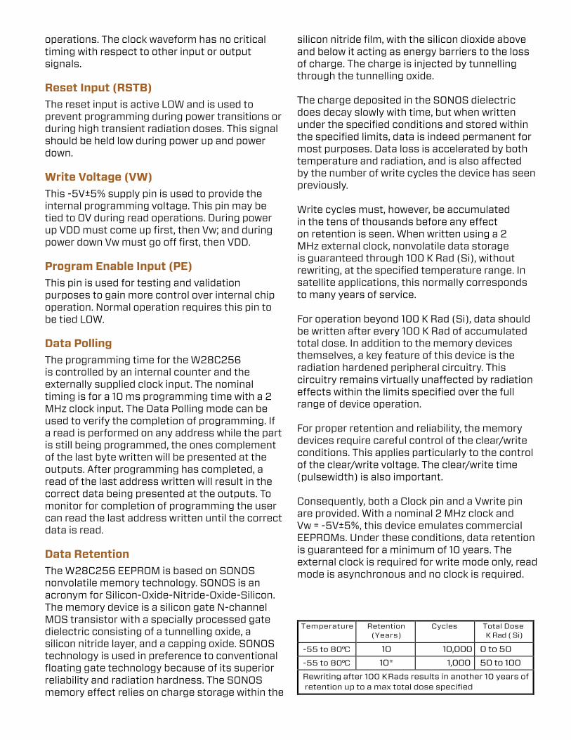
AC Operating Characteristics (Write Operations)TA = -55 to + 125°C, VDD = 5V ±5%, unless otherwise specified
Limits
Symbol Parameter Min MAX Units Test Conditions
fC Clock Frequency 1 2 MHz Write Mode (Note 1)
tWC Write Cycle Time 10 ms fc = 2 MHz (Note 1)
tAS Address Setup Time 0 ns
tAH Address Hold Time 150 ns
tCS Write Setup Time 0 ns
tCH Write Hold Time 0 ns
tCW CEB Pulse Width 150 ns
tOES OEB High Setup Time 10 ns
tOEH OEB High Hold Time 10 ns
tWP WEB Pulse Width 150 ns
tDS Data Setup Time 0 ns
tDH Data Hold Time 60 ns
tBLC Byte Load Cycle 0.2 250 µs fc = 2 MHz
tLP Last Byte Loaded toData Polling Output
300 µs fc = 2 MHz
Note:1. Verified by functional testing.
Write Cycle
ADDRESS
WE
DATA
CE
OE
tAS tAH
tCStWP
tCH
tBLC
tDS tDH
tOEH
tOES
tCW
PAGE LOAD
Note: All or a portion of the 64 byte page may be loaded prior to writing, but the entire page is always writtenwith the contents of the data latches. Single byte data modification is not supported.
DATA Polling
BYTE 0 BYTE I BYTE N BYTE N
tWC
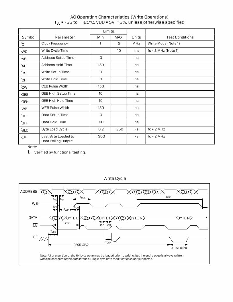
AC Operating Characteristics (Read Operations)TA = -55 to 125°C, VDD = 5V ±5%, unless otherwise specified
Limits
Symbol Parameter Min MAX Units Test Conditions
tRC Read Cycle Time 250 ns
tCE CEB Access Time 250 ns OEB = VIL
tAA Address Access Time 250 ns CEB = OEB = VIL
tOE OEB Access Time 125 ns CEB = VIL
tDF OEB or CEB High to Output HiZ
130 ns CEB OR OEB = VIL IO = ±3mA
tOH Output Hold from AddressChange
0 ns CEB = OEB =VIL (Note 1)
tOHZ OEB High to High Z Output 25 ns IO = ±3mA
Note:1. Verified by functional testing.
Read Cycle
tRC
tCE
tOE
tAA
tOH
ADDRESS
DATA
CE
OE
tAA
tOHZ
tDF
AC Test Loads and Input Waveforms
90%90%4.75V
10%10%
OV<10 ns<10 ns
INPUT PULSES
CAPACITANCE TA = 25°C f = 1 MHz
Symbol Parameter MAX Conditions
CIN Input Capacitance 5pF Vin = 0
COUT External Load Capacitance 70pF AC Operations
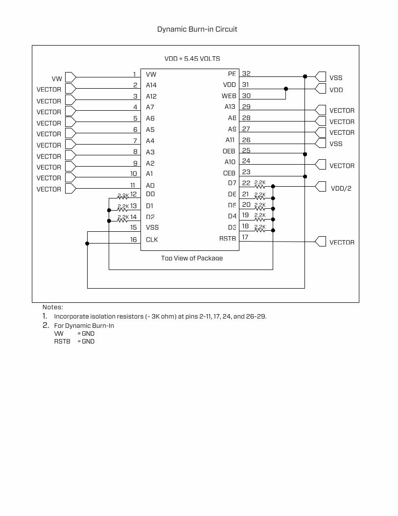
Dynamic Burn-in Circuit
VW
A14
A12
A7
A6
A5
A4
A3
A2
A1
VECTOR
VECTOR
VECTOR
VECTOR
VECTOR
VECTOR
VECTOR
VECTOR
VECTOR
VECTOR
VECTOR
VECTOR
VECTOR
VSS
VSS
VDD
VECTOR
VECTOR
D1
D2
VSS
CLK
PE
VDD
WEB
A13
A8
A9
A11
OEB
A10
CEBD7
D6
D5
D4
D3
RSTB
1
2
3
4
5
6
7
8
9
10
1112
13
14
15
16
VW
VDD = 5.45 VOLTS
Top View of Package
2.2K
2.2K
2.2K
2.2K
2.2K
2.2K
2.2K
2.2K
Notes:1. Incorporate isolation resistors (~ 3K ohm) at pins 2-11, 17, 24, and 26-29.2. For Dynamic Burn-In
VW = GNDRSTB = GND
AODO
32
31
30
29
28
27
26
25
24
23
22
21
20
19
18
17
VDD/2
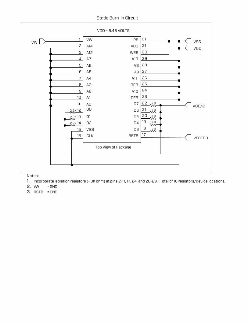
Static Burn-in Circuit
VW
A14
A12
A7
A6
A5
A4
A3
A2
A1
VDD
VSS
VECTOR
D1
D2
VSS
CLK
PE
VDD
WEB
A13
A8
A9
A11
OEB
A10
CEB
D7
D6
D5
D4
D3
RSTB
1
2
3
4
5
6
7
8
9
10
11
12
13
14
15
16
VW
VDD = 5.45 VOLTS
Top View of Package
2.2K
2.2K
2.2K
2.2K
2.2K
2.2K
2.2K
2.2K
Notes:1. Incorporate isolation resistors (~ 3K ohm) at pins 2-11, 17, 24, and 26-29. (Total of 16 resistors/device location).2. VW = GND3. RSTB = GND
31
31
30
29
28
27
26
25
24
23
22
21
20
19
18
17
AODO
VDD/2
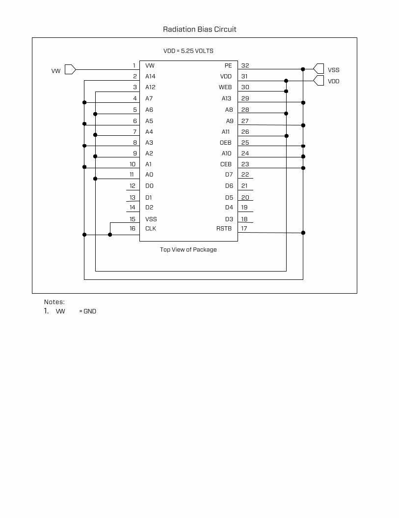
Radiation Bias Circuit
VW
A14
A12
A7
A6
A5
A4
A3
A2
A1
A0
VDD
VSS
D0
D1
D2
VSS
CLK
32
31
30
29
28
27
26
25
24
23
22
21
20
19
18
17
PE
VDD
WEB
A13
A8
A9
A11
OEB
A10
CEB
D7
D6
D5
D4
D3
RSTB
1
2
3
4
5
6
7
8
9
11
12
13
15
16
VW
VDD = 5.25 VOLTS
Top View of Package
10
14
Notes:1. VW = GND
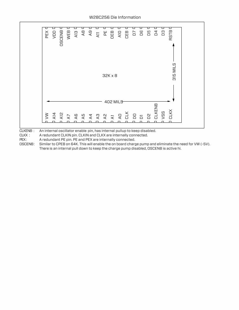
W28C256 Die Information
VW
PE
X
A14
VD
D
A12
OS
CE
NB
A4
A9
A10
A7
WE
B
A3
A11
CLK
CE
B
A6
A13
A2
PE
D7
D2
VS
S
D5
D3
A5
A8
A1
OE
B
D1
D6
CLK
EN
B
CLK
X3
15 M
ILS
402 MILS
32K x 8
D4
RS
TB
CLKENB : An internal oscillator enable pin, has internal pullup to keep disabled.CLKX : A redundant CLKIN pin. CLKIN and CLKX are internally connected.PEX : A redundant PE pin. PE and PEX are internally connected.OSCENB: Similar to CPEB on 64K. This will enable the on board charge pump and eliminate the need for VW (-5V).
There is an internal pull down to keep the charge pump disabled, OSCENB is active hi.
AO
DO
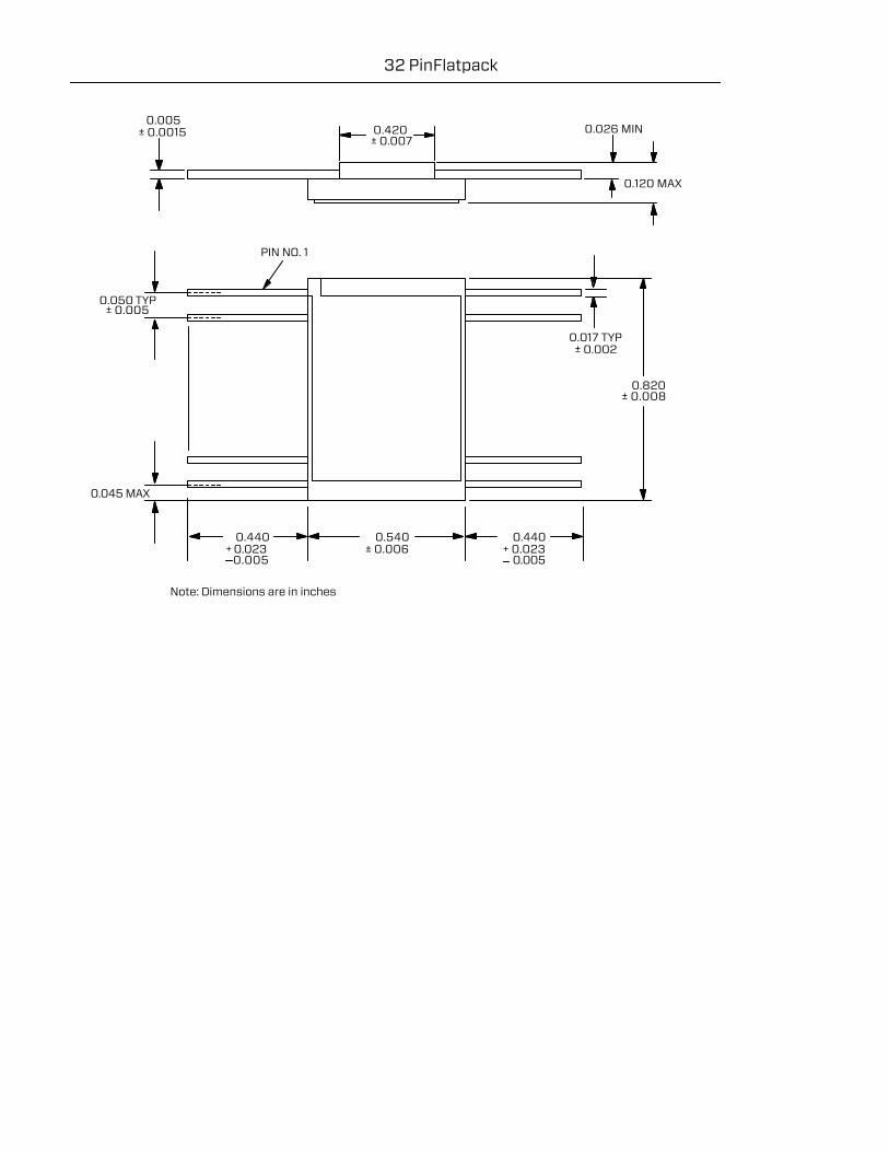
32 Pin Flatpack
PIN NO. 1
0.017 TYP ± 0.002
0.820± 0.008
0.420± 0.007
0.005± 0.0015
0.120 MAX
0.026 MIN
0.440+ 0.023
0.005
0.540± 0.006
0.440+ 0.023
0.005
0.045 MAX
Note: Dimensions are in inches
0.050 TYP ± 0.005
www.northropgrumman.comSpecifications and features subject to change without notice.© 2013 Northrop Grumman Systems CorporationAll rights reserved.
MS-216-AMG-0913 A330: 13-19142013 RM Graphics
For more information, please contact:
Northrop Grumman Corporation Electronic Systems P.O. Box 1521, MS 3D14 Baltimore, MD 21203 USA Email: [email protected]
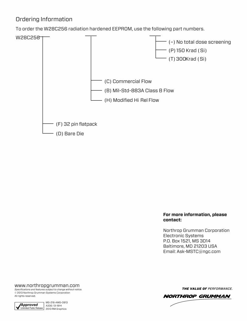
Ordering Information
To order the W28C256 radiation hardened EEPROM, use the following part numbers.
W28C256
(F) 32 pin flatpack
(D) Bare Die
(C) Commercial Flow
(B) Mil-Std-883A Class B Flow
(H) Modified Hi Rel Flow
(–) No total dose screening
(P) 150 Krad (Si)
(T) 300 Krad (Si)