Embed Size (px)
Citation preview

○Product structure:Silicon monolithic integrated circuit ○This product is not designed protection against radioactive rays .
1/34 TSZ02201-0RBR0A300100-1-2© 2012 ROHM Co., Ltd. All rights reserved.
2013.04.04 Rev.001TSZ22111・14・001
www.rohm.com
Datasheet
CMOS LDO Regulators for Portable Equipments
1ch 200mA CMOS LDO Regulators BUxxSA4 series
●General Description
BUxxSA4 series are high-performance CMOS LDO regulators with output current ability of up to 200-mA. These devices have excellent noise and load response characteristics despite of its low circuit current consumption of 40µA. They are most appropriate for various applications such as power supplies for logic IC, RF, and camera modules.
●Features
High Output Voltage Accuracy: ±0.6% (±15mV on VOUT<2.5V)
High Ripple Rejection: 70 dB (Typ, 1 kHz,) Compatible with small ceramic capacitor
(Cin=Cout=0.47 µF) Low Current Consumption: 40 µA Output Voltage ON/OFF control Built-in Over Current Protection Circuit (OCP) Built-in Thermal Shutdown Circuit (TSD) Adopting ultra-small WLCSP UCSP50L1
●Applications Portable devices Camera modules Other electronic devices using microcontrollers or
logic circuits
●Key Specifications Input Power Supply Voltage Range: 1.7V to 5.5V Output Current Range: 0 to 200mA Operating Temperature Range: -40℃ to +85℃ Output Voltage Lineup: 1.8V,2.5V,2.55V
2.8V,3.0V,3.3V Output Voltage Accuracy: ±0.6% Circuit Current: 40µA(Typ.) Standby Current: 0μA (Typ.)
●Package W(Typ.) x D(Typ.) x H(Max.) UCSP50L1(BUXXSA4WGWL) 0.8mm x 0.8mm x 0.5mm
●Typical Application Circuit
Figure 1. Typical Application Circuit
Vin
Cin Cout
VoutVIN VOUT
STBYGND
On
Off
BUxxSD2MG-M
Vin
Cin Cout
VoutVIN VOUT
STBYGND
On
Off
BUxxSD2MG-M
Vin
Cin Cout
VoutVIN VOUT
STBYGND
On
Off
BUxxSD2MG-MBUxxSA4

DatasheetDatasheet
2/34 TSZ02201-0RBR0A300100-1-2© 2012 ROHM Co., Ltd. All rights reserved.
2013.04.04 Rev.001
www.rohm.com
TSZ22111・15・001
BUxxSA4 series
Figure 2. Block diagram
Cin(min)=0.47µF (Ceramic)
Cout(min)=0.47µF (Ceramic)
●Pin Configuration ●Pin Description
Pin No. Symbol Function
A1 GND GND Pin
A2 STBY Output Control Pin (High:ON, Low:OFF)
B1 VOUT Output Pin
B2 VIN Input Pin
●Block Diagram
1
3
5
2
Cin
VIN
GND
STBY VSTBY
VOUT VOUT
Cout
VREF
STBY
TSD
VIN
N.C. 4
OCP
Top View
(Mark Side)
A
B
1 2
Bottom View
B
A
1 2
1Pin Mark

DatasheetDatasheet
3/34 TSZ02201-0RBR0A300100-1-2© 2012 ROHM Co., Ltd. All rights reserved.
2013.04.04 Rev.001
www.rohm.com
TSZ22111・15・001
BUxxSA4 series
●Absolute Maximum Ratings
Parameter Symbol Rating Unit
Power Supply Voltage VMAX -0.3 to +6.5 V
Power Dissipation Pd 410(*1) mW
Maximum Junction Temperature Tjmax +125 ℃
Operating Temperature Range Topr -40 to +85 ℃
Storage Temperature Range Tstg -55 to +125 ℃
(*1) Derate by 4.1mW/℃ when operating above Ta=25℃.(When mounted on a board 63mm×55mm×1.6mm glass-epoxy board, 9 layer) ●Recommended Operating Ratings
Parameter Symbol Limit Unit
Input Power Supply Voltage Range VIN 1.7 to 5.5 V
●Recommended Operating Conditions
Parameter Symbol Rating
Unit Conditions Min. Typ. Max.
Input capacitor Cin 0.47(*2) 1.0 - µF A ceramic capacitor is recommended.
Output capacitor Cout 0.47(*2) 1.0 - µF A ceramic capacitor is recommended.
(*2) Set the value of the capacitor so that it does not fall below the minimum value. Take into consideration the temperature characteristics, DC device characteristics, and degradation with time.
DatasheetDatasheet
4/34 TSZ02201-0RBR0A300100-1-2© 2012 ROHM Co., Ltd. All rights reserved.
2013.04.04 Rev.001
www.rohm.com
TSZ22111・15・001
BUxxSA4 series
●Electrical Characteristics (Unless otherwise noted, Ta=-25℃, VIN=VOUT+1.0V(*6), VSTBY=1.5V, Cin=1μF, Cout=1μF.)
PARAMETER Symbol Limit Unit Conditions MIN. TYP. MAX.
Output Voltage 1 VOUT1
VOUT ×0.994 VOUT
VOUT ×1.006 V
IOUT = 10μA, VOUT≧2.5V
VOUT -15mV
VOUT +15mV IOUT = 10μA, VOUT<2.5V
Output Voltage 2 VOUT2
VOUT ×0.98
VOUT
VOUT ×1.02
V
IOUT=0 to 200mA, VOUT≧2.5V VIN=VOUT+0.5 to 5.5V Ta=-40 to +85℃(*3,4,5)
VOUT -50mV
VOUT +50mV
IOUT=0 to 200mA, VOUT<2.5V VIN=3.0 to 5.5V Ta=-40 to +85℃(*3,4,5)
Circuit Current 1 IGND1 - 40 65 μA IOUT=0mA Circuit Current 2 IGND2 - 40 80 μA Ta=-40 to +85℃(*4), IOUT=0mA Circuit Current (STBY) ICCST - - 1.0 μA STBY=0V Ripple Rejection Ratio1 RR1 - 70 - dB VRR=-20dBv,fRR=1kHz,IOUT=10mA Ripple Rejection Ratio2 RR2 - 55 - dB VRR=-20dBv,fRR=10kHz,IOUT=10mA Ripple Rejection Ratio3 RR3 - 45 - dB VRR=-20dBv,fRR=100kHz,IOUT=10mA
Dropout Voltage VDROP - 80 150 mV VIN=0.98×VOUT, IOUT=100mA
Ta=-40 to +85℃, VOUT≧2.5V
- 150 360 mV VIN=0.98×VOUT, IOUT=100mA Ta=-40 to +85℃, VOUT<2.5V
Load transient resp. VLOT - ±65 - mV Io=1 to 150mA,Trise=Tfall=1μs, VIN=VOUT+1.0V(*4)
Line Transient resp. VLIT - ±5 - mV VIN=VOUT+0.5 to VOUT+1.0V, Trise=Tfall=10μs
Output noise voltage VNOIS - 30 - μVrms Bandwidth 10 to 100kHz
Startup time TST - 100 300 μsec Output voltage settled within tolerancies
Line Regulation VDLI - 2 8 mV IOUT=10mA VIN=VOUT+0.5 to 5.5V(*5)
Load Regulation1 VDLO1 - 2 8 mV IOUT=1 to 100mA Load Regulation2 VDLO2 - 4 16 mV IOUT=1 to 200mA Maximum Output Current IOMAX 200 - - mA VIN=VOUT+1.0V(*6) Limit Current ILMAX 250 400 - mA Vo=VOUT×0.98 Short Current ISHORT - 100 200 mA Vo=0V STBY Pin Current ISTBY - - 4.0 μA
Ta=-40 to +85℃ STBY Control Voltage
ON VSTBH 1.1 - VIN V OFF VSTBL -0.2 - 0.5 V
(*3) Operating conditions are limited by Pd. (*4) Typical values apply for Ta=25℃. (*5) VIN=3.0V to 5.0V for VOUT<2.5V. (*6) VIN=3.5V for VOUT<2.5V.

DatasheetDatasheet
5/34 TSZ02201-0RBR0A300100-1-2© 2012 ROHM Co., Ltd. All rights reserved.
2013.04.04 Rev.001
www.rohm.com
TSZ22111・15・001
BUxxSA4 series
●Reference data BU18SA4WGWL (Unless otherwise specified, Ta=25℃.)
Figure 3. Output Voltage vs. Input Voltage Figure 4. Line Regulation
Figure 5. GND Current vs. Input Voltage Figure 6. Load Regulation
0.00
0.20
0.40
0.60
0.80
1.00
1.20
1.40
1.60
1.80
0 0.5 1 1.5 2 2.5 3 3.5 4 4.5 5 5.5
Input Voltage (V)
Out
put V
olta
ge (
V)
Temp=25°CVIN=STBY
IOUT=0uAIOUT=50mAIOUT=200mA
1.70
1.72
1.74
1.76
1.78
1.80
1.82
1.84
1.86
1.88
1.90
0 0.5 1 1.5 2 2.5 3 3.5 4 4.5 5 5.5
Input Voltage (V)
Out
put V
olta
ge (
V)
Temp=25°CVIN=STBY
IOUT=0uAIOUT=50mAIOUT=200mA
0
20
40
60
80
100
0 0.5 1 1.5 2 2.5 3 3.5 4 4.5 5 5.5
Input Voltage (V)
GN
D C
urre
nt (
uA)
VIN=STBYIOUT=0uA
Temp=-40°CTemp=25°CTemp=85°C
1.70
1.72
1.74
1.76
1.78
1.80
1.82
1.84
1.86
1.88
1.90
0 50 100 150 200
Output Current (mA)
Out
put
Vol
tage
(V
)
VIN=2.8VSTBY=1.5V
Temp=-40°C
Temp=25°C
Temp=85°C

DatasheetDatasheet
6/34 TSZ02201-0RBR0A300100-1-2© 2012 ROHM Co., Ltd. All rights reserved.
2013.04.04 Rev.001
www.rohm.com
TSZ22111・15・001
BUxxSA4 series
●Reference data BU18SA4WGWL (Unless otherwise specified, Ta=25℃.)
Figure 7. GND Current vs. Output Current Figure 8. OCP Threshold
Figure 9. Output Voltage vs. Temperature Figure 10. GND Current vs. Temperature
0
20
40
60
80
100
120
0 50 100 150 200Output Current (mA)
GN
D C
urre
nt (u
A)
VIN=2.8VSTBY=1.5VTemp=-40°C
Temp=25°C
Temp=85°
0.0
0.5
1.0
1.5
2.0
2.5
0 100 200 300 400 500Output Current (A)
Out
put V
olta
ge (V
)
VIN=5.5V
VIN=2.3V
VIN=2.8V
Temp=25°C
STBY=1.5V
1.74
1.76
1.78
1.80
1.82
1.84
1.86
-40 -15 10 35 60 85
Temperature (°C)
Out
put V
olta
ge (V
)
VIN=2.8VSTBY=1.5VIo=0.1mA
0
10
20
30
40
50
60
-40 -15 10 35 60 85
Temperature (°C)
GN
D C
urre
nt (u
A)
VIN=2.8VSTBY=1.5VIo=0.1mA
DatasheetDatasheet
7/34 TSZ02201-0RBR0A300100-1-2© 2012 ROHM Co., Ltd. All rights reserved.
2013.04.04 Rev.001
www.rohm.com
TSZ22111・15・001
BUxxSA4 series
●Reference data BU18SA4WGWL (Unless otherwise specified, Ta=25℃.)
0
10
20
30
40
50
60
70
80
90
100
-40 -15 10 35 60 85
Temperature (°C)
GN
D C
urre
nt (a
t STB
Y) (
nA) VIN=5.5V
STBY=0V
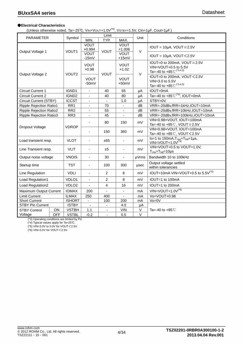
Figure 11. STBY Threshold Figure 12. GND Current (at STBY) vs. Temperature
Figure 13. STBY Pin Current vs. STBY Pin Voltage
0.0
0.5
1.0
1.5
2.0
2.5
3.0
3.5
0 0.25 0.5 0.75 1 1.25 1.5STBY Voltage (V)
Out
put V
olta
ge (
V)
Temp=-40°CTemp=25°CTemp=85°C
VIN=2.8VIo=0.1mA
0.0
0.2
0.4
0.6
0.8
1.0
1.2
1.4
1.6
0 0.5 1 1.5 2 2.5 3 3.5 4 4.5 5 5.5STBY Voltage (V)
STBY
Pin
Cur
rent
(uA)
Temp=-40°CTemp=25°CTemp=85°C

DatasheetDatasheet
8/34 TSZ02201-0RBR0A300100-1-2© 2012 ROHM Co., Ltd. All rights reserved.
2013.04.04 Rev.001
www.rohm.com
TSZ22111・15・001
BUxxSA4 series
●Reference data BU18SA4WGWL (Unless otherwise specified, Ta=25℃,Cin = Cout =1μF.)
Figure 14. Ripple Rejection vs. Input Voltage Figure 15. Ripple Rejection vs. Freqency
Figure 16. Output Noise vs. Output Current
0
10
20
30
40
50
60
70
80
90
100
100 1000 10000 100000Frequency (Hz)
Rip
ple
Rej
ectio
n (d
B)
Ta = 25℃
Iout = 10mA
0
10
20
30
40
50
60
70
80
1.5 2 2.5 3 3.5 4 4.5 5 5.5Input Voltage (V)
Rip
ple
Rej
ectio
n (d
B)
Ta = 25℃
Iout = 10mAVIN_AC = -20dBV
0
10
20
30
40
50
60
70
0 50 100 150 200Output Current (mA)
Out
put N
oise
(uVr
ms)
Ta = 25℃
Vin = 2.8V
0.01
0.1
1
10
10 100 1000 10000 100000Frequency (Hz)
Out
put N
oise
Den
sity
(uV
/ √H
z) Ta = 25℃
Iout = 10mA
Figure 17. Output Noise Density vs. Frequency

DatasheetDatasheet
9/34 TSZ02201-0RBR0A300100-1-2© 2012 ROHM Co., Ltd. All rights reserved.
2013.04.04 Rev.001
www.rohm.com
TSZ22111・15・001
BUxxSA4 series
●Reference data BU18SA4WGWL (Unless otherwise specified, Ta=25℃,Cin = Cout =1μF.)
Figure 20. Discharge time ( Rout = none ) Figure 21. Discharge time ( Rout = 9 ohm )
Figure 19. Startup time ( Rout = 9 ohm )
Figure 18. Startup time ( Rout = none )
0.0
2.0
1.0
STB
Y V
oltage
(V)
0.0
2.0
1.0
Outp
ut
Vola
tage
(V)
STBY=0V→1.5V
VOUT
Cout=0.47uF
Cout=1uF
Cout=2.2uF
1V/div
1V/div
VIN=2.8V
20us/div
STBY=0V→1.5V
Cout=0.47uF
Cout=1uF
Cout=2.2uF
0.0
2.0
1.0
STB
Y V
oltage
(V)
0.0
2.0
1.0
Outp
ut
Vola
tage
(V)
1V/div
1V/div
VIN=2.8V
20us/div
STBY=1.5V→0V
VOUT Cout=0.47uF
Cout=1uF
Cout=2.2uF
0.0
2.0
1.0
STB
Y V
oltage
(V)
Outp
ut
Vola
tage
(V)
1V/div
1V/div
VIN=2.8V
400ms/div
0.0
2.0
1.0
3.0
STBY=1.5V→0V
VOUTCout=0.47uF
Cout=1uF
Cout=2.2uF
0.0
2.0
1.0
STB
Y V
oltage
(V)
0.0
2.0
1.0
Outp
ut
Vola
tage
(V)
1V/div
1V/div
VIN=2.8V
20us/div

DatasheetDatasheet
10/34 TSZ02201-0RBR0A300100-1-2© 2012 ROHM Co., Ltd. All rights reserved.
2013.04.04 Rev.001
www.rohm.com
TSZ22111・15・001
BUxxSA4 series
●Reference data BU18SA4WGWL (Unless otherwise specified, Ta=25℃, Cin = Cout =1μF.)
Figure 22. Load response ( Iout = 1mA → 150mA)
Figure 23. Load response ( Iout = 150mA → 1mA)
Figure 24. Line response ( Vin= 2.3V → 2.9V)
Figure 25. Line response ( Vin= 2.9V → 2.3V)
Outp
ut
Vola
tage
(V)
0
200
100
Outpu
t Curre
nt(m
A)
1.75
1.85
1.80
1.70
VOUT 50mV/div
100mA/div
2.0us/div
IOUT=1mA→150mA
VIN=2.8VSTBY=2.8VCout=1uF
50mV/div
2.0us/div
1.80
1.90
1.85
1.75
IOUT=150mA→1mA
100mA/div
VIN=2.8VSTBY=2.8VCout=1uF
0
200
100
Outpu
t Curre
nt(m
A)
Outp
ut
Vola
tage
(V)
VOUT
VIN=2.3V→2.9V
1.79
1.81
1.80
Outp
ut
Vola
tage
(V)
10mV/div
200mV/div
10us/div
2.3
2.7
2.5
2.9
STBY=2.3V→2.9VIo=10mACout=1uF
Inpu
t Voltage
(V)
VIN=2.9V→2.3V
VOUT
200mV/div
10us/div2.3
2.7
2.5
2.9
1.79
1.81
1.80
Outp
ut
Vola
tage
(V)
STBY=2.9V→2.3VIo=10mACout=1uF
Inpu
t Voltage
(V)
DatasheetDatasheet
11/34 TSZ02201-0RBR0A300100-1-2© 2012 ROHM Co., Ltd. All rights reserved.
2013.04.04 Rev.001
www.rohm.com
TSZ22111・15・001
BUxxSA4 series
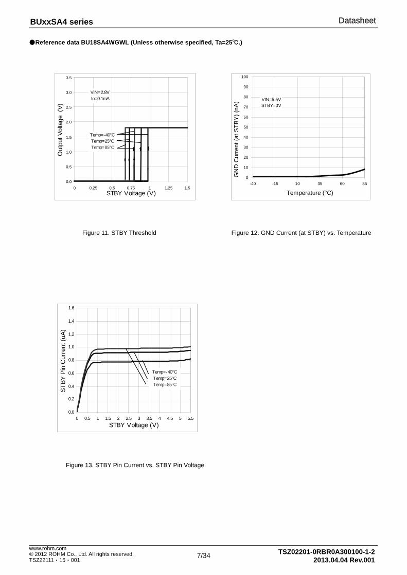
●Reference data BU28SA4WGWL (Unless otherwise specified, Ta=25℃.)
Figure 26. Output Voltage vs. Input Voltage Figure 27. Line Regulation
Figure 28. GND Current vs. Input Voltage Figure 29. Load Regulation
0.0
0.4
0.8
1.2
1.6
2.0
2.4
2.8
3.2
0 0.5 1 1.5 2 2.5 3 3.5 4 4.5 5 5.5
Input Voltage (V)
Out
put V
olta
ge (
V)
Temp=25°C
IO=0uAIO=50mAIO=200mA
VIN=STBY
2.70
2.73
2.75
2.78
2.80
2.83
2.85
2.88
2.90
0 0.5 1 1.5 2 2.5 3 3.5 4 4.5 5 5.5
Input Voltage (V)
Out
put V
olta
ge (V
) Temp=25°C
IO=0uAIO=50mAIO=200mA
VIN=STBY
0
20
40
60
80
100
0 0.5 1 1.5 2 2.5 3 3.5 4 4.5 5 5.5
Input Voltage (V)
GN
D C
urre
nt (u
A) IO=0uAVIN=STBY
Temp=-40°CTemp=25°CTemp=85°C
2.70
2.74
2.78
2.82
2.86
2.90
0 50 100 150 200Output Current (mA)
Out
put V
olta
ge (V
)
VIN=3.8VSTBY=1.5V
Temp=-40°C
Temp=25°C
Temp=85°C

DatasheetDatasheet
12/34 TSZ02201-0RBR0A300100-1-2© 2012 ROHM Co., Ltd. All rights reserved.
2013.04.04 Rev.001
www.rohm.com
TSZ22111・15・001
BUxxSA4 series
●Reference data BU28SA4WGWL (Unless otherwise specified, Ta=25℃.)
Figure 30. GND Current vs. Output Current Figure 31. OCP Threshold
Figure 32. Output Voltage vs. Temperature Figure 33. GND Current vs. Temperature
0
20
40
60
80
100
120
0 50 100 150 200
Output Current (mA)
GN
D C
urre
nt (u
A)
VIN=3.8VSTBY=1.5VTemp=-40°C
Temp=25°C
Temp=85°C
0.0
0.5
1.0
1.5
2.0
2.5
3.0
3.5
0 100 200 300 400 500
Output Current (A)
Out
put V
olta
ge (V
)
VIN=3.3VVIN=3.8VVIN=5.5V
2.75
2.76
2.77
2.78
2.79
2.80
2.81
2.82
2.83
2.84
2.85
-40 -15 10 35 60 85
Temperature (°C)
Out
put V
olta
ge (V
)
VIN=3.8VSTBY=1.5VIo=0.1mA
0
10
20
30
40
50
60
-40 -15 10 35 60 85
Temperature (°C)
GN
D C
urre
nt (u
A)
VIN=3.8VSTBY=1.5VIo=0.1mA

DatasheetDatasheet
13/34 TSZ02201-0RBR0A300100-1-2© 2012 ROHM Co., Ltd. All rights reserved.
2013.04.04 Rev.001
www.rohm.com
TSZ22111・15・001
BUxxSA4 series
●Reference data BU28SA4WGWL (Unless otherwise specified, Ta=25℃.)
0
10
20
30
40
50
60
70
80
90
100
-40 -15 10 35 60 85
Temperature (°C)
GN
D C
urre
nt (a
t STB
Y) (
nA) VIN=5.5V
STBY=0V
Figure 34. STBY Threshold Figure 35. GND Current (at STBY) vs. Temperature
Figure 36. STBY Pin Current vs. STBY Voltage
0.0
0.5
1.0
1.5
2.0
2.5
3.0
3.5
0 0.25 0.5 0.75 1 1.25 1.5
STBY Voltage (V)
Out
put V
olta
ge (
V)
Temp=-40°CTemp=25°CTemp=85°C
VIN=3.8VIo=0.1mA
0.0
0.2
0.4
0.6
0.8
1.0
1.2
1.4
1.6
0 0.5 1 1.5 2 2.5 3 3.5 4 4.5 5 5.5
STBY Voltage (V)
STB
Y P
in C
urre
nt (u
A)
Temp=-40°CTemp=25°CTemp=85°C
0
20
40
60
80
100
120
140
160
180
200
0 50 100 150 200Output Current (mA)
Dro
pout
Vol
tage
(mV
)
VIN = 0.98 x VOUTSTBY=1.5V
Temp=-40°C
Temp=25°C
Temp=85°C
Figure 37. Dropuout Voltage vs. Output Current

DatasheetDatasheet
14/34 TSZ02201-0RBR0A300100-1-2© 2012 ROHM Co., Ltd. All rights reserved.
2013.04.04 Rev.001
www.rohm.com
TSZ22111・15・001
BUxxSA4 series
●Reference data BU28SA4WGWL (Unless otherwise specified, Ta=25℃,Cin = Cout =1μF.)
Figure 38. Ripple Rejection vs. Input Voltage Figure 39. Ripple Rejection vs. Frequency
Figure 40. Output Noise vs. Output Current
0
10
20
30
40
50
60
70
80
2.8 3.3 3.8 4.3 4.8 5.3Input Voltage (V)
Rip
ple
Rej
ectio
n (d
B)
Ta = 25℃
Iout = 10mAVIN_AC = -20dBV
0
10
20
30
40
50
60
70
80
100 1000 10000 100000
Frequency (Hz)
Rip
ple
Rej
ectio
n (d
B)
Ta = 25℃
Iout = 10mA
0
10
20
30
40
50
60
70
0 50 100 150 200Output Current (mA)
Out
put N
oise
(uVr
ms)
Ta = 25℃
Vin = 3.8V
0.01
0.1
1
10
10 100 1000 10000 100000Frequency (Hz)
Out
put N
oise
Den
sity
(uV
/ √H
z) Ta = 25℃
Iout = 10mA
Figure 41. Output Noise Density vs. Frequency

DatasheetDatasheet
15/34 TSZ02201-0RBR0A300100-1-2© 2012 ROHM Co., Ltd. All rights reserved.
2013.04.04 Rev.001
www.rohm.com
TSZ22111・15・001
BUxxSA4 series
●Reference data BU28SA4WGWL (Unless otherwise specified, Ta=25℃,Cin = Cout =1μF.)
Figure 44. Discharge time ( Rout = none ) Figure 45. Discharge time ( Rout = 14 ohm )
Figure 42. Startup time ( Rout = none ) Figure 43. Startup time ( Rout = 14 ohm )
STBY=0V→1.5V
Cout=0.47uFCout=1uF
Cout=2.2uF
0.0
2.0
1.0
STB
Y V
oltage
(V)
0.0
2.0
1.0
Outp
ut
Vola
tage
(V)
1V/div
1V/div
VIN=3.8V
20us/div
3.0
VOUT
VOUT
STBY=0V→1.5V
Cout=0.47uF
Cout=1uF
Cout=2.2uF
0.0
2.0
1.0
STB
Y V
oltage
(V)
1V/div
1V/div
VIN=3.8V
20us/div
0.0
2.0
1.0
Outp
ut
Vola
tage
(V)
3.0
VOUT
STBY=1.5V→0V
VOUT
Cout=0.47uF
Cout=1uF
Cout=2.2uF
0.0
2.0
1.0
STB
Y V
oltage
(V)
0.0
2.0
1.0
Outp
ut
Vola
tage
(V)
1V/div
1V/div
VIN=3.8V
400ms/div
3.0
STBY=1.5V→0V
VOUT
Cout=0.47uF
Cout=1uFCout=2.2uF
0.0
2.0
1.0
STB
Y V
oltage
(V)
0.0
2.0
1.0
Outp
ut
Vola
tage
(V)
1V/div
1V/div
20us/div
VIN=3.8V
3.0

DatasheetDatasheet
16/34 TSZ02201-0RBR0A300100-1-2© 2012 ROHM Co., Ltd. All rights reserved.
2013.04.04 Rev.001
www.rohm.com
TSZ22111・15・001
BUxxSA4 series
●Reference data BU28SA4WGWL (Unless otherwise specified, Ta=25℃,Cin = Cout =1μF.)
Figure 46. Load response ( Iout = 1mA → 150mA)
Figure 47. Load response ( Iout = 150mA → 1mA)
Figure 48. Line response ( Vin= 3.3V → 3.9V) Figure 49. Line response ( Vin= 3.9V → 3.3V)
VOUT
Outp
ut
Vola
tage
(V)
50mV/div
100mA/div
2.0us/div
0
200
100
Outpu
t Curre
nt(m
A)
2.75
2.85
2.80
2.70
IOUT=1mA→150mA
VIN=3.8VSTBY=3.8VCout=1uF
Outpu
t Curre
nt(m
A)
VOUT 50mV/div
2.0us/div
Outp
ut
Vola
tage
(V)
2.80
2.80
2.85
2.75
IOUT=150mA→1mA
100mA/div
VIN=3.8VSTBY=3.8VCout=1uF
0
200
100
VIN=3.3V→3.9V
VOUT2.79
2.81
2.80
Outp
ut
Vola
tage
(V)
10mV/div
200mV/div
10us/div
3.3
3.7
3.5
3.9
STBY=3.3V→3.9VIOUT=10mACout=1uF
Inpu
t Voltage
(V)
VIN=3.9V→3.3V
VOUT 10mV/div
200mV/div
10us/div
STBY=3.9V→3.3VIOUT=10mACout=1uF
2.79
2.81
2.80
Outp
ut
Vola
tage
(V) 3.3
3.7
3.5
3.9
Inpu
t Voltage
(V)

DatasheetDatasheet
17/34 TSZ02201-0RBR0A300100-1-2© 2012 ROHM Co., Ltd. All rights reserved.
2013.04.04 Rev.001
www.rohm.com
TSZ22111・15・001
BUxxSA4 series
●Reference data BU30SA4WGWL (Unless otherwise specified, Ta=25℃.)
Figure 50. Output Voltage vs. Input Voltage Figure 51. Line Regulation
Figure 52. GND Current vs. Input Voltage Figure 53. Load Regulation
0.0
0.5
1.0
1.5
2.0
2.5
3.0
3.5
0 0.5 1 1.5 2 2.5 3 3.5 4 4.5 5 5.5
Input Volatage (V)
Out
put V
olta
ge (V
)
Temp=25°CVIN=STBY
IOUT=0uAIOUT=50mAIOUT=200mA
2.90
2.92
2.94
2.96
2.98
3.00
3.02
3.04
3.06
3.08
3.10
0 0.5 1 1.5 2 2.5 3 3.5 4 4.5 5 5.5
Input Voltage (V)
Out
put
Volta
ge (
V)
Temp=25°CVIN=STBY
IOUT=0uAIOUT=50mAIOUT=200mA
0
20
40
60
80
100
0 0.5 1 1.5 2 2.5 3 3.5 4 4.5 5 5.5
Input Voltage (V)
GN
D C
urre
nt (
uA)
Temp=-40°CTemp=25°CTemp=85°C
VIN=STBYIOUT=0uA
2.90
2.92
2.94
2.96
2.98
3.00
3.02
3.04
3.06
3.08
3.10
0 50 100 150 200
Output Current (mA)
Out
put
Volta
ge (V
)
VIN=4.0VSTBY=1.5V
Temp=-40°C
Temp=25°C
Temp=85°C

DatasheetDatasheet
18/34 TSZ02201-0RBR0A300100-1-2© 2012 ROHM Co., Ltd. All rights reserved.
2013.04.04 Rev.001
www.rohm.com
TSZ22111・15・001
BUxxSA4 series
●Reference data BU30SA4WGWL (Unless otherwise specified, Ta=25℃.)
Figure 54. GND Current vs. Output Current Figure 55. OCP Threshold
Figure 56. Output Voltage vs. Temperature Figure 57. GND Current vs. Temperature
0.0
0.5
1.0
1.5
2.0
2.5
3.0
3.5
0 100 200 300 400 500
Output Current (mA)
Out
put V
olta
ge (V
)
VIN=5.5V
VIN=3.5V
VIN=4.0V
Temp=25°CSTBY=1.5V
0
20
40
60
80
100
120
0 50 100 150 200
Output Current (mA)
GN
D C
urre
nt (
uA)
Temp=-40°C VIN=4.0VSTBY=1.5V
Temp=85°C
Temp=25°C
2.90
2.92
2.94
2.96
2.98
3.00
3.02
3.04
3.06
3.08
3.10
-40 -15 10 35 60 85Temperature (°C)
Out
put V
olta
ge (V
)
VCC=4.0VSTBY=1.5V
IOUT=0.1mA
0
10
20
30
40
50
60
-40 -15 10 35 60 85
Temperature (°C)
GN
D C
urre
nt (
uA)
VIN=4.0VSTBY=1.5VIOUT=0.1mA

DatasheetDatasheet
19/34 TSZ02201-0RBR0A300100-1-2© 2012 ROHM Co., Ltd. All rights reserved.
2013.04.04 Rev.001
www.rohm.com
TSZ22111・15・001
BUxxSA4 series
●Reference data BU30SA4WGWL (Unless otherwise specified, Ta=25℃.)
0
10
20
30
40
50
60
70
80
90
100
-40 -15 10 35 60 85
Temperature (°C)
GN
D C
urre
nt (a
t STB
Y) (
nA) VIN=5.5V
STBY=0V
Figure 59. GND Current(at STBY) vs. Temperature
Figure 60. STBY Pin Voltage vs. STBY Pin Current Figure 61. Dropout Voltage vs. Output Current
0.0
0.5
1.0
1.5
2.0
2.5
3.0
3.5
0 0.25 0.5 0.75 1 1.25 1.5STBY Voltage (V)
Out
put V
olta
ge (V
)
Temp=85°C
Temp=-40°C
Temp=25°C
VIN=4.0VIOUT=0.1mA
0.0
0.2
0.4
0.6
0.8
1.0
1.2
1.4
1.6
0 0.5 1 1.5 2 2.5 3 3.5 4 4.5 5 5.5
STBY Voltage (V)
STB
Y P
in C
urre
nt (u
A)
Temp=-40°CTemp=25°CTemp=85°C
0
20
40
60
80
100
120
140
160
180
200
0 50 100 150 200
Output Current (mA)
Dro
pout
Vol
tage
(mV)
VCC = 0.98 x VOUTSTBY=1.5V
Temp=-40°C
Temp=25°C
Temp=85°C
Figure 58. STBY Threshold

DatasheetDatasheet
20/34 TSZ02201-0RBR0A300100-1-2© 2012 ROHM Co., Ltd. All rights reserved.
2013.04.04 Rev.001
www.rohm.com
TSZ22111・15・001
BUxxSA4 series
●Reference data BU30SA4WGWL (Unless otherwise specified, Ta=25℃,Cin = Cout =1μF.)
Figure 62. Ripple Rejection vs. Input Voltage Figure 63. Ripple Rejection vs. Frequency
Figure 64. Output Noise vs. Output Current
0
10
20
30
40
50
60
70
80
3 3.5 4 4.5 5 5.5Input Voltage (V)
Rip
ple
Rej
ectio
n (d
B)
Ta = 25℃
Iout = 10mAVIN_AC = -20dBV
0
10
20
30
40
50
60
70
80
100 1000 10000 100000
Frequency (Hz)
Rip
ple
Rej
ectio
n (d
B)
Ta = 25℃
Iout = 10mA
0
10
20
30
40
50
60
70
0 50 100 150 200Output Current (mA)
Out
put N
oise
(uVr
ms)
Ta = 25℃
Vin = 4.0V
0.01
0.1
1
10
10 100 1000 10000 100000Frequency (Hz)
Out
put N
oise
Den
sity
(uV
/ √H
z) Ta = 25℃
Iout = 10mA
Figure 65. Output Noise Density vs. Frequency

DatasheetDatasheet
21/34 TSZ02201-0RBR0A300100-1-2© 2012 ROHM Co., Ltd. All rights reserved.
2013.04.04 Rev.001
www.rohm.com
TSZ22111・15・001
BUxxSA4 series
●Reference data BU30SA4WGWL (Unless otherwise specified, Ta=25℃,Cin = Cout =1μF.)
Figure 68. Discharge time ( Rout = none ) Figure 69. Discharge time ( Rout = 15 ohm )
Figure 66. Startup time ( Rout = none ) Figure 67. Startup time ( Rout = 15 ohm )
STBY=0V→1.5V
VOUT
Cout=0.47uFCout=1uF
Cout=2.2uF
0.0
2.0
1.0
STB
Y V
oltage
(V)
0.0
2.0
1.0
Outp
ut
Vola
tage
(V) 1V/div
1V/div
VIN=4.0V
20us/div
3.0
STBY=0V→1.5V
VOUT
Cout=0.47uF
Cout=1uFCout=2.2uF
0.0
2.0
1.0
STB
Y V
oltage
(V)
0.0
2.0
1.0
Outp
ut
Vola
tage
(V)
1V/div
1V/div
VIN=4.0V
20us/div
3.0
STBY=1.5V→0V
VOUT
Cout=0.47uFCout=1uF
Cout=2.2uF
0.0
2.0
1.0
STB
Y V
oltage
(V)
Outp
ut
Vola
tage
(V)
1V/div
1V/div
VIN=4.0V
400ms/div
0.0
2.0
1.0
3.0
STBY=1.5V→0V
VOUT
Cout=0.47uFCout=1uF
Cout=2.2uF
0.0
2.0
1.0
STB
Y V
oltage
(V)
0.0
2.0
1.0
Outp
ut
Vola
tage
(V)
1V/div
20us/div3.0
VIN=4.0V
1V/div

DatasheetDatasheet
22/34 TSZ02201-0RBR0A300100-1-2© 2012 ROHM Co., Ltd. All rights reserved.
2013.04.04 Rev.001
www.rohm.com
TSZ22111・15・001
BUxxSA4 series
●Reference data BU30SA4WGWL (Unless otherwise specified, Ta=25℃,Cin = Cout =1μF.)
Figure 70. Load response ( Iout = 1mA → 150mA)
Figure 71. Load response ( Iout = 150mA → 1mA)
Figure 72. Line response ( Vin= 3.5 V → 4.1 V) Figure 73. Line response ( Vin= 4.1 V → 3.5 V)
Outpu
t Curre
nt(m
A)
VOUT
Outp
ut
Vola
tage
(V)
50mV/div
100mA/div
2.0us/div
0
200
100
2.95
3.05
3.00
2.9
IOUT=1mA→150mA
VIN = 4.0 VSTBY = 1.5 VCout = 1 uF
VOUT 50mV/div
2.0us/div
Outp
ut
Vola
tage
(V)
IOUT=150mA→1mA
100mA/div
VIN = 4.0 VSTBY = 1.5 VCout = 1 uF
0
200
100
Outpu
t Curre
nt(m
A)
2.95
3.05
3.00
3.10
VIN=3.5V→4.1V
VOUT2.99
3.01
3.00
Outp
ut
Vola
tage
(V)
10mV/div
200mV/div
10us/div
3.5
3.9
3.7
4.1
STBY=3.5V→4.1VIOUT=10mACout=1uF
Inpu
t Voltage
(V)
VIN=4.1V→3.5V
VOUT 10mV/div
200mV/div
10us/div3.5
3.9
3.7
4.1
2.99
3.01
3.00
Outp
ut
Vola
tage
(V)
STBY=4.1V→3.5VIOUT=10mACout=1uF
Inpu
t Voltage
(V)

DatasheetDatasheet
23/34 TSZ02201-0RBR0A300100-1-2© 2012 ROHM Co., Ltd. All rights reserved.
2013.04.04 Rev.001
www.rohm.com
TSZ22111・15・001
BUxxSA4 series
●Reference data BU33SA4WGWL (Unless otherwise specified, Ta=25℃.)
0.0
0.5
1.0
1.5
2.0
2.5
3.0
3.5
0 0.5 1 1.5 2 2.5 3 3.5 4 4.5 5 5.5Input Voltage (V)
Out
put V
olta
ge (
V)
Temp=25°CVIN=STBY
IOUT=0uAIOUT=50mAIOUT=200mA
3.20
3.22
3.24
3.26
3.28
3.30
3.32
3.34
3.36
3.38
3.40
0 0.5 1 1.5 2 2.5 3 3.5 4 4.5 5 5.5
Input Voltage (V)
Out
put V
olta
ge (
V)
Temp=25°CVIN=STBY
IOUT=0uAIOUT=50mAIOUT=200mA
0
20
40
60
80
100
0 0.5 1 1.5 2 2.5 3 3.5 4 4.5 5 5.5
Input Voltage (V)
GND
Cur
rent
(uA
)
Temp=-40°CTemp=25°CTemp=85°C
VIN=STBYIOUT=0uA
3.20
3.22
3.24
3.26
3.28
3.30
3.32
3.34
3.36
3.38
3.40
0 50 100 150 200
Output Current (mA)
Out
put V
olta
ge (V
)
Temp=25°C
Temp=85°CTemp=-40°C
VIN=4.3VSTBY=1.5V
Figure 74. Output Voltage vs. Input Voltage Figure 75. Line Regulation
Figure 76. GND Current vs. Input Voltage Figure 77. Load Regulation

DatasheetDatasheet
24/34 TSZ02201-0RBR0A300100-1-2© 2012 ROHM Co., Ltd. All rights reserved.
2013.04.04 Rev.001
www.rohm.com
TSZ22111・15・001
BUxxSA4 series
●Reference data BU33SA4WGWL (Unless otherwise specified, Ta=25℃.)
0.0
0.5
1.0
1.5
2.0
2.5
3.0
3.5
0 100 200 300 400 500
Output Current (mA)
Out
put v
olta
ge (V
) VIN=3.8V
VIN=4.3V
VIN=5.5V
0
20
40
60
80
100
120
0 50 100 150 200
Output Current (mA)
GN
D C
urre
nt (µ
A)
Temp=85°C
Temp=25°C
Temp=-40°C
Figure 78. GND Current vs. Output Current Figure 79. OCP Threshold
3.20
3.22
3.24
3.26
3.28
3.30
3.32
3.34
3.36
3.38
3.40
-40 -15 10 35 60 85
Temperature (°C)
Out
put V
olta
ge (V
)
VIN=4.3VSTBY=1.5V
IOUT=0.1mA
0
10
20
30
40
50
60
-40 -15 10 35 60 85
Temperature (°C)
GND
Cur
rent
(µA)
VIN=4.3VSTBY=1.5VIOUT=0.1mA
Figure 80. Output Voltage vs. Temperature Figure 81. GND Current vs. Temperature

DatasheetDatasheet
25/34 TSZ02201-0RBR0A300100-1-2© 2012 ROHM Co., Ltd. All rights reserved.
2013.04.04 Rev.001
www.rohm.com
TSZ22111・15・001
BUxxSA4 series
●Reference data BU33SA4WGWL (Unless otherwise specified, Ta=25℃.)
0
10
20
30
40
50
60
70
80
90
100
-40 -15 10 35 60 85
Temperature (°C)
GN
D C
urre
nt (a
t STB
Y) (
nA) VIN=5.5V
STBY=0V
0.0
0.5
1.0
1.5
2.0
2.5
3.0
3.5
0 0.25 0.5 0.75 1 1.25 1.5
STBY Voltage (V)
Out
put V
olta
ge (V
) Temp=-40°C
Temp=85°C
Temp=25°C
VIN=4.3VIOUT=0.1mA
Figure 82. STBY Threshold Figure 83. GND Current (at STBY) vs. Temperature
0.0
0.2
0.4
0.6
0.8
1.0
1.2
1.4
1.6
0 0.5 1 1.5 2 2.5 3 3.5 4 4.5 5 5.5
STBY Voltage (V)
STBY
Pin
Cur
rent
(µA)
Temp=-40°CTemp=25°CTemp=85°C
0
20
40
60
80
100
120
140
160
180
200
0 50 100 150 200
Output Current (mA)
Drop
out V
OUT
[V]
Temp=-40°C
Temp=85°C
Temp=25°C
VIN=0.98×VOUT
STBY=1.5V
Figure 84. STBY Pin Current vs. STBY Voltage Figure 85. Dropout Voltage vs. Output Current

DatasheetDatasheet
26/34 TSZ02201-0RBR0A300100-1-2© 2012 ROHM Co., Ltd. All rights reserved.
2013.04.04 Rev.001
www.rohm.com
TSZ22111・15・001
BUxxSA4 series
●Reference data BU33SA4WGWL (Unless otherwise specified, Ta=25℃,Cin = Cout =1μF.)
0
10
20
30
40
50
60
70
80
3.3 3.8 4.3 4.8 5.3Input Voltage (V)
Rip
ple
Rej
ectio
n (d
B)
Ta = 25℃
Iout = 10mAVIN_AC = -20dBV
0
10
20
30
40
50
60
70
80
100 1000 10000 100000Frequency (Hz)
Rip
ple
Rej
ectio
n (d
B)
Ta = 25℃
Iout = 10mA
Figure 86. Ripple Rejection vs. Input Voltage Figure 87. Ripple Rejection vs. Frequency
0
10
20
30
40
50
60
70
0 50 100 150 200Output Current (mA)
Out
put N
oise
(uVr
ms)
Ta = 25℃
Vin = 4.3V
0.01
0.1
1
10
10 100 1000 10000 100000Frequency (Hz)
Out
put N
oise
Den
sity
(uV
/ √
Hz)
Figure 88. Output Noise vs. Output Current Figure 89. Output Noise Density vs. Frequency

DatasheetDatasheet
27/34 TSZ02201-0RBR0A300100-1-2© 2012 ROHM Co., Ltd. All rights reserved.
2013.04.04 Rev.001
www.rohm.com
TSZ22111・15・001
BUxxSA4 series
●Reference data BU33SA4WGWL (Unless otherwise specified, Ta=25℃,Cin = Cout =1μF.)
VOUT
STBY=0V→1.5V
Cout=0.47uFCout=1uF
Cout=2.2uF
0.0
2.0
1.0
STB
Y V
oltage
(V)
0.0
2.0
1.0
Outp
ut
Vola
tage
(V)
1V/div
1V/div
VIN=4.3V
20us/div
3.0VOUT
STBY=0V→1.5V
Cout=0.47uFCout=1uFCout=2.2uF
0.0
2.0
1.0
STB
Y V
oltage
(V)
1V/div
1V/div
VIN=4.3V
20us/div
0.0
2.0
1.0
Outp
ut
Vola
tage
(V)
3.0VOUT
Figure 90. Startup time ( Rout = none ) Figure 91. Startup time ( Rout = 16.5 ohm )
STBY=1.5V→0V
VOUT
Cout=0.47uFCout=1uF
Cout=2.2uF
0.0
2.0
1.0
STB
Y V
oltage
(V)
0.0
2.0
1.0
Outp
ut
Vola
tage
(V)
1V/div
1V/div
VIN=4.3V
400ms/div
3.0
STBY=1.5V→0V
VOUT
Cout=0.47uFCout=1uF
Cout=2.2uF
0.0
2.0
1.0
STB
Y V
oltage
(V)
0.0
2.0
1.0
Outp
ut
Vola
tage
(V)
1V/div
1V/div
20us/div
VIN=4.3V
3.0
Figure 92. Discharge time ( Rout = none ) Figure 93. Discharge time ( Rout = 16.5 ohm )

DatasheetDatasheet
28/34 TSZ02201-0RBR0A300100-1-2© 2012 ROHM Co., Ltd. All rights reserved.
2013.04.04 Rev.001
www.rohm.com
TSZ22111・15・001
BUxxSA4 series
●Reference data BU33SA4WGWL (Unless otherwise specified, Ta=25℃,Cin = Cout =1μF.)
VIN=3.8V→4.4V
VOUT3.29
3.31
3.30
Outp
ut
Vola
tage
(V)
10mV/div
200mV/div
10us/div
3.8
4.2
4.0
4.4
STBY=3.8V→4.4VIo=10mACout=1uF
Inpu
t Voltage
(V)
VIN=4.4V→3.8V
VOUT 10mV/div
200mV/div
10us/div
STBY=4.4V→3.8VIo=10mACout=1uF
3.29
3.31
3.30
Outp
ut
Vola
tage
(V) 3.8
4.2
4.0
4.4
Inpu
t Voltage
(V)
VOUT
Outp
ut
Vola
tage
(V)
50mV/div
100mA/div
2.0us/div
0
200
100
Outpu
t Curre
nt(m
A)
3.25
3.35
3.30
3.20
IOUT=1mA→150mA
VIN=4.3VSTBY=4.3VCout=1uF
Outpu
t Curre
nt(m
A)
VOUT 50mV/div
2.0us/div
Outp
ut
Vola
tage
(V)
3.30
3.40
3.35
3.25
IOUT=150mA→1mA
100mA/div
VIN=4.3VSTBY=4.3VCout=1uF
0
200
100
Figure 94. Load response ( Iout = 1mA → 150mA)
Figure 95. Load response ( Iout = 150mA → 1mA)
Figure 96. Line response ( Vin= 3.8 V → 4.4 V)
Figure 97. Line response ( Vin= 4.4 V → 3.8 V)

DatasheetDatasheet
29/34 TSZ02201-0RBR0A300100-1-2© 2012 ROHM Co., Ltd. All rights reserved.
2013.04.04 Rev.001
www.rohm.com
TSZ22111・15・001
BUxxSA4 series
Figure 99. Stability area characteristics (Example)
●Input/Output Capacitor
It is recommended that an input capacitor is placed near pins between the VCC pin and GND as well as an output capacitor between the output pin and GND. The input is valid when the power supply impedance is high or when the PCB trace has significant length. For the output capacitor, the greater the capacitance, the more stable the output will be depending on the load and line voltage variations. However, please check the actual functionality of this capacitor by mounting it on a board for the actual application. Ceramic capacitors usually have different, thermal and equivalent series resistance characteristics, and may degrade gradually over continued use. For additional details, please check with the manufacturer, and select the best ceramic capacitor for your application
●Equivalent Series Resistance (ESR) of a Ceramic Capacitor
Capacitors generally have ESR (equivalent series resistance) and it operates stably in the ESR-IOUT area shown on the right. Since ceramic capacitors, tantalum capacitors, electrolytic capacitors, etc. generally have different ESR, please check the ESR of the capacitor to be used and use it within the stability area range shown in the right graph for evaluation of the actual application.
0.01
0.1
1
10
100
0 50 100 150 200IOUT[mA]
ESR
[Ω]
Stable regionCin=Co=0.47uF Ta=-40 to 85℃
Unstable region
Stable region
Capacity value of ceramic capacitor - DC bias characteristics(Example)
-100
-90
-80
-70
-60
-50
-40
-30
-20
-10
0
10
0 0.5 1 1.5 2 2.5 3 3.5 4
DC Bias Voltage [V]
Cap
acita
nce
Cha
nge
[%]
10-V withstand voltageB1characteristicsGRM188B11A105KA61D
10-V withstand voltageB characteristics
6.3-V withstand voltageB characteristics
4-V withstand voltageX6S characteristics
10-V withstand voltageF characteristics
10-V withstand voltageF characteristics
Figure 98. Capacity-bias characteristics

DatasheetDatasheet
30/34 TSZ02201-0RBR0A300100-1-2© 2012 ROHM Co., Ltd. All rights reserved.
2013.04.04 Rev.001
www.rohm.com
TSZ22111・15・001
BUxxSA4 series
●Power Dissipation (Pd) As for power dissipation, an estimate of heat reduction characteristics and internal power consumption of IC are shown, so please use these for reference. Since power dissipation changes substantially depending on the implementation conditions (board size, board thickness, metal wiring rate, number of layers and through holes, etc.), it is recommended to measure Pd on a set board. Exceeding the power dissipation of IC may lead to deterioration of the original IC performance, such as causing the operation of the thermal shutdown circuit or reduction in current capability. Therefore, be sure to prepare sufficient margin within power dissipation for usage. Calculation of the maximum internal power consumption of IC (PMAX) PMAX=(VIN-VOUT)×IOMAX Where : VIN=Input voltage VOUT= Output voltage IOMAX: Maximum output current) ○Measurement conditions
Evaluation board
Layout of Board for Measurement
Top Layer (Top View) Bottom Layer (Top View)
Measurement State With board implemented (Wind speed 0 m/s) Board Material Glass epoxy resin (9 layers)
Board Size 63 mm x 55 mm x 1.6 mm
Wiring Rate
Top layer Metal (GND) wiring rate: Approx. 0% Bottom layer Metal (GND) wiring rate: Approx. 50%
Through Hole Diameter 0.5mm x 6 holes Power Dissipation 0.41W Thermal Resistance θja=243.9°C/W
* Please design the margin so that PMAX is less than Pd (PMAX<Pd) within the usage temperature range
Figure 100. UCSP50L1(BUXXSA4WGWL) Power dissipation heat reduction characteristics (Reference)
0
0.1
0.2
0.3
0.4
0.5
0 25 50 75 100 125
Ta[℃]
Pd
[W]
0.41W 評価基板1
85

DatasheetDatasheet
31/34 TSZ02201-0RBR0A300100-1-2© 2012 ROHM Co., Ltd. All rights reserved.
2013.04.04 Rev.001
www.rohm.com
TSZ22111・15・001
BUxxSA4 series
●I/O Equivalence Circuits
B1 pin (VOUT) A1 pin (GND) A2 pin (STBY) B2 pin (VIN)
Figure 101. Input / Output equivalent circuit
VOUT
VIN
VOUT
VIN
DatasheetDatasheet
32/34 TSZ02201-0RBR0A300100-1-2© 2012 ROHM Co., Ltd. All rights reserved.
2013.04.04 Rev.001
www.rohm.com
TSZ22111・15・001
BUxxSA4 series
●Operational Notes 1) Absolute maximum ratings
This product is produced with strict quality control, however it may be destroyed if operated beyond its absolute maximum ratings. In addition, it is impossible to predict all destructive situations such as short-circuit modes, open circuit modes, etc. Therefore, i t is impor tant to cons ider c i rcu i t protect ion measures, l ike adding a fuse, in case the IC is operated in a spec ia l mode exceeding the absolute maximum rat ings.
2) GND Potential GND potential must be the lowest potential of all pins of the IC at all operating conditions. Ensure that no pins are at a voltage below the ground pin at any time, even during transient condition.
3) Setting of Heat Carry out the heat design that have adequate margin considering Pd of actual working states.
4) Pin Short and Mistake Fitting When mounting the IC on the PCB, pay attention to the orientation of the IC. If there is mistake in the placement, the IC may be burned up.
5) Actions in Strong Magnetic Field
Using the IC within a strong magnetic field may cause the IC to malfunction. 6) Mutual Impedance
Use short and wide wiring tracks for the power supply and ground to keep the mutual impedance as small as possible. Use a capacitor to keep ripple to a minimum.
7) STBY Pin Voltage
To enable standby mode for all channels, set the STBY pin to 0.5 V or less, and for normal operation, to 1.1 V or more. Setting STBY to a voltage between 0.5 and 1.1 V may cause malfunction and should be avoided. Keep transition time between high and low (or vice versa) to a minimum. Additionally, if STBY is shorted to VIN, the IC will switch to standby mode and disable the output discharge circuit, causing a temporary voltage to remain on the output pin. If the IC is switched on again while this voltage is present, overshoot may occur on the output. Therefore, in applications where these pins are shorted, the output should always be completely discharged before turning the IC on.
8) Over Current Protection Circuit Over current and short circuit protection is built-in at the output, and IC destruction is prevented at the time of load short circuit. These protection circuits are effective in the destructive prevention by sudden accidents, please avoid applications to where the over current protection circuit operates continuously.
9) Thermal Shutdown This IC has Thermal Shutdown Circuit (TSD Circuit). When the temperature of IC Chip is higher than 175℃, the output is turned off by TSD Circuit. TSD Circuit is only designed for protecting IC from thermal over load. Therefore it is not recommended that you design application where TSD will work in normal condition.
10) Actions under Strong light A strong light like a halogen lamp may be caused malfunction. In our testing, fluorescence light and white LED causes little effects for the IC, but infrared light causes strong effects on the IC. The IC should be shielded from light like sunrays or halogen lamps.
11) Output capacitor To prevent oscillation at output, it is recommended that the IC be operated at the stable region shown in Figure 99. It operates at the capacitance of more than 0.47μF. As capacitance is larger, stability becomes more stable and characteristic of output load fluctuation is also improved.

DatasheetDatasheet
33/34 TSZ02201-0RBR0A300100-1-2© 2012 ROHM Co., Ltd. All rights reserved.
2013.04.04 Rev.001
www.rohm.com
TSZ22111・15・001
BUxxSA4 series
●Ordering Information ●Physical Dimension Tape and Reel Information ●Marking Diagram
∗ Order quantity needs to be multiple of the minimum quantity.
<Tape and Reel information>
Embossed carrier tapeTape
Quantity
Direction of feed The direction is the 1pin of product is at the upper left when you hold
reel on the left hand and you pull out the tape on the right hand
3000pcs
E2
( )
Direction of feed
Reel1pin
(Unit : mm)
UCSP50L1(BUXXSA4WGWL)
S
0.06 S
0.55
MA
X
0.1±
0.05
A
B
BA0.05
0.2±0.05
4-φ0.25±0.05
21
0.2±
0.05
B
A 0.4
0.4
1PIN MARK
0.8±0.05
0.8±
0.05
x x
Marking
Lot No.
1Pin Mark
Part No. MarkingBU18SA4WGWL C3BU25SA4WGWL C9BU2FSA4WGWL FABU28SA4WGWL E2BU30SA4WGWL E5BU33SA4WGWL E8
E 2
ROHMPart No.
Output voltagexx=18:1.8Vxx=25:2.5Vxx=2F:2.55Vxx=28:2.8Vxx=30:3.0Vxx=33:3.3V
Series nameSA4W:High-speedSA4W:load response SA4W:Low noise
SA4W:Shutdown SW
PackageGWL: UCSP50L1GWL: (BUXXSA4WGWL)
Packaging and formingspecificationsE2:Embossed tape and reel UCSP50L1(BUXXSA4WGWL)
4 W G W L -B U x x S A

DatasheetDatasheet
34/34 TSZ02201-0RBR0A300100-1-2© 2012 ROHM Co., Ltd. All rights reserved.
2013.04.04 Rev.001
www.rohm.com
TSZ22111・15・001
BUxxSA4 series
●Revision History
Date Revision Changes
04.Apr.2013 001 New Release

DatasheetDatasheet
Notice - GE Rev.002© 2014 ROHM Co., Ltd. All rights reserved.
Notice Precaution on using ROHM Products
1. Our Products are designed and manufactured for application in ordinary electronic equipments (such as AV equipment, OA equipment, telecommunication equipment, home electronic appliances, amusement equipment, etc.). If you intend to use our Products in devices requiring extremely high reliability (such as medical equipment (Note 1), transport equipment, traffic equipment, aircraft/spacecraft, nuclear power controllers, fuel controllers, car equipment including car accessories, safety devices, etc.) and whose malfunction or failure may cause loss of human life, bodily injury or serious damage to property (“Specific Applications”), please consult with the ROHM sales representative in advance. Unless otherwise agreed in writing by ROHM in advance, ROHM shall not be in any way responsible or liable for any damages, expenses or losses incurred by you or third parties arising from the use of any ROHM’s Products for Specific Applications.
(Note1) Medical Equipment Classification of the Specific Applications JAPAN USA EU CHINA
CLASSⅢ CLASSⅢ
CLASSⅡb CLASSⅢ
CLASSⅣ CLASSⅢ
2. ROHM designs and manufactures its Products subject to strict quality control system. However, semiconductor
products can fail or malfunction at a certain rate. Please be sure to implement, at your own responsibilities, adequate safety measures including but not limited to fail-safe design against the physical injury, damage to any property, which a failure or malfunction of our Products may cause. The following are examples of safety measures:
[a] Installation of protection circuits or other protective devices to improve system safety [b] Installation of redundant circuits to reduce the impact of single or multiple circuit failure
3. Our Products are designed and manufactured for use under standard conditions and not under any special or extraordinary environments or conditions, as exemplified below. Accordingly, ROHM shall not be in any way responsible or liable for any damages, expenses or losses arising from the use of any ROHM’s Products under any special or extraordinary environments or conditions. If you intend to use our Products under any special or extraordinary environments or conditions (as exemplified below), your independent verification and confirmation of product performance, reliability, etc, prior to use, must be necessary:
[a] Use of our Products in any types of liquid, including water, oils, chemicals, and organic solvents [b] Use of our Products outdoors or in places where the Products are exposed to direct sunlight or dust [c] Use of our Products in places where the Products are exposed to sea wind or corrosive gases, including Cl2,
H2S, NH3, SO2, and NO2
[d] Use of our Products in places where the Products are exposed to static electricity or electromagnetic waves [e] Use of our Products in proximity to heat-producing components, plastic cords, or other flammable items [f] Sealing or coating our Products with resin or other coating materials [g] Use of our Products without cleaning residue of flux (even if you use no-clean type fluxes, cleaning residue of
flux is recommended); or Washing our Products by using water or water-soluble cleaning agents for cleaning residue after soldering
[h] Use of the Products in places subject to dew condensation
4. The Products are not subject to radiation-proof design. 5. Please verify and confirm characteristics of the final or mounted products in using the Products. 6. In particular, if a transient load (a large amount of load applied in a short period of time, such as pulse. is applied,
confirmation of performance characteristics after on-board mounting is strongly recommended. Avoid applying power exceeding normal rated power; exceeding the power rating under steady-state loading condition may negatively affect product performance and reliability.
7. De-rate Power Dissipation (Pd) depending on Ambient temperature (Ta). When used in sealed area, confirm the actual
ambient temperature. 8. Confirm that operation temperature is within the specified range described in the product specification. 9. ROHM shall not be in any way responsible or liable for failure induced under deviant condition from what is defined in
this document.
Precaution for Mounting / Circuit board design 1. When a highly active halogenous (chlorine, bromine, etc.) flux is used, the residue of flux may negatively affect product
performance and reliability. 2. In principle, the reflow soldering method must be used; if flow soldering method is preferred, please consult with the
ROHM representative in advance. For details, please refer to ROHM Mounting specification

DatasheetDatasheet
Notice - GE Rev.002© 2014 ROHM Co., Ltd. All rights reserved.
Precautions Regarding Application Examples and External Circuits 1. If change is made to the constant of an external circuit, please allow a sufficient margin considering variations of the
characteristics of the Products and external components, including transient characteristics, as well as static characteristics.
2. You agree that application notes, reference designs, and associated data and information contained in this document
are presented only as guidance for Products use. Therefore, in case you use such information, you are solely responsible for it and you must exercise your own independent verification and judgment in the use of such information contained in this document. ROHM shall not be in any way responsible or liable for any damages, expenses or losses incurred by you or third parties arising from the use of such information.
Precaution for Electrostatic
This Product is electrostatic sensitive product, which may be damaged due to electrostatic discharge. Please take proper caution in your manufacturing process and storage so that voltage exceeding the Products maximum rating will not be applied to Products. Please take special care under dry condition (e.g. Grounding of human body / equipment / solder iron, isolation from charged objects, setting of Ionizer, friction prevention and temperature / humidity control).
Precaution for Storage / Transportation 1. Product performance and soldered connections may deteriorate if the Products are stored in the places where:
[a] the Products are exposed to sea winds or corrosive gases, including Cl2, H2S, NH3, SO2, and NO2 [b] the temperature or humidity exceeds those recommended by ROHM [c] the Products are exposed to direct sunshine or condensation [d] the Products are exposed to high Electrostatic
2. Even under ROHM recommended storage condition, solderability of products out of recommended storage time period may be degraded. It is strongly recommended to confirm solderability before using Products of which storage time is exceeding the recommended storage time period.
3. Store / transport cartons in the correct direction, which is indicated on a carton with a symbol. Otherwise bent leads
may occur due to excessive stress applied when dropping of a carton. 4. Use Products within the specified time after opening a humidity barrier bag. Baking is required before using Products of
which storage time is exceeding the recommended storage time period.
Precaution for Product Label QR code printed on ROHM Products label is for ROHM’s internal use only.
Precaution for Disposition When disposing Products please dispose them properly using an authorized industry waste company.
Precaution for Foreign Exchange and Foreign Trade act Since our Products might fall under controlled goods prescribed by the applicable foreign exchange and foreign trade act, please consult with ROHM representative in case of export.
Precaution Regarding Intellectual Property Rights 1. All information and data including but not limited to application example contained in this document is for reference
only. ROHM does not warrant that foregoing information or data will not infringe any intellectual property rights or any other rights of any third party regarding such information or data. ROHM shall not be in any way responsible or liable for infringement of any intellectual property rights or other damages arising from use of such information or data.:
2. No license, expressly or implied, is granted hereby under any intellectual property rights or other rights of ROHM or any
third parties with respect to the information contained in this document.
Other Precaution 1. This document may not be reprinted or reproduced, in whole or in part, without prior written consent of ROHM. 2. The Products may not be disassembled, converted, modified, reproduced or otherwise changed without prior written
consent of ROHM. 3. In no event shall you use in any way whatsoever the Products and the related technical information contained in the
Products or this document for any military purposes, including but not limited to, the development of mass-destruction weapons.
4. The proper names of companies or products described in this document are trademarks or registered trademarks of
ROHM, its affiliated companies or third parties.

DatasheetDatasheet
Notice – WE Rev.001© 2014 ROHM Co., Ltd. All rights reserved.
General Precaution 1. Before you use our Pro ducts, you are requested to care fully read this document and fully understand its contents.
ROHM shall n ot be in an y way responsible or liabl e for fa ilure, malfunction or acci dent arising from the use of a ny ROHM’s Products against warning, caution or note contained in this document.
2. All information contained in this docume nt is current as of the issuing date and subj ect to change without any prior
notice. Before purchasing or using ROHM’s Products, please confirm the la test information with a ROHM sale s representative.
3. The information contained in this doc ument is provi ded on an “as is” basis and ROHM does not warrant that all
information contained in this document is accurate an d/or error-free. ROHM shall not be in an y way responsible or liable for any damages, expenses or losses incurred by you or third parties resulting from inaccuracy or errors of or concerning such information.