Embed Size (px)
Citation preview

SOCSA Slides: CMOS Basics
© Institute for Integrated Systems Technische Universität München www.lis.ei.tum.de
CMOS Basics
System-on-Chip
Solutions & Architectures A. Herkersdorf
© Institute for
Integrated Systems
A. Herkersdorf SoC - CMOS Basics - 2
Module outline
Introduction to CMOS
Where is CMOS?
What is CMOS?
Why is CMOS so attractive?
How does CMOS work?
Basics
CMOS Device Basics
Static CMOS Logic
Sequential Logic CMOS and FSM design
Power Consumption Of Static CMOS Logic

SOCSA Slides: CMOS Basics
© Institute for
Integrated Systems
A. Herkersdorf SoC - CMOS Basics - 3
Where is CMOS ?
DRAM
µP ASIC
FPGA
DS
P
© Institute for
Integrated Systems
A. Herkersdorf SoC - CMOS Basics - 4
Where is CMOS ? Where is CMOS ?
There !
DRAM
µP ASIC
FPGA
DS
P

SOCSA Slides: CMOS Basics
© Institute for
Integrated Systems
A. Herkersdorf SoC - CMOS Basics - 5
Where is CMOS ? Where is CMOS ?
Gartner:
World-wide semiconductor revenue 2002: 155 B USD
© Institute for
Integrated Systems
A. Herkersdorf SoC - CMOS Basics - 6
Where isn‘t CMOS?
Bipolar Analog wireless
power amplifiers
recievers
very high speed digital communications
interface electronics
mm-wave defense
SiGe / GaAs ultra high speed
BiCMOS mixed-signal
high speed

SOCSA Slides: CMOS Basics
© Institute for
Integrated Systems
A. Herkersdorf SoC - CMOS Basics - 7
Metal (Poly-Si) Oxide (SiO2) Semiconductor
CMOS - What is it?
nMOS pMOS
p+
n
n+
p
The C in CMOS signals the combination of p- and n-MOSFETS Complementary
gnd Vdd
The Channel type gives the prefix of the transistor
© Institute for
Integrated Systems
A. Herkersdorf SoC - CMOS Basics - 8
Why CMOS ?
Electrical Reasons Low power dissipation
Noise immunity
Clean logic levels
One supply voltage
Cascadable
Economical Reasons Easy to design
Fabrication well understood
Highly integrateable
Si-Wafer
SiO2-Layer
Light
Light patterns
Photoresist
Etching
Doping Atoms (P or As)
Photolithographic Mask Photoresist
Poly-Si-Layer
Lithography
Process
Deposition

SOCSA Slides: CMOS Basics
© Institute for
Integrated Systems
A. Herkersdorf SoC - CMOS Basics - 9
Vdd Vdd 0 V
How does it work?
gnd Vdd 0 V -Vdd
gnd
inversion
inversion
n+
n+
p+
p+
p
p
© Institute for
Integrated Systems
A. Herkersdorf SoC - CMOS Basics - 10
How does it work?
Source(gnd)
Vgs
Vgs
0
Vds
ID
Vds=const.
0
Vt
Vt

SOCSA Slides: CMOS Basics
© Institute for
Integrated Systems
A. Herkersdorf SoC - CMOS Basics - 11
How does it work?
Source(gnd)
Vgs
Vds
0
Vds
ID
Vds= Vgs(1)-Vt
0
Vt
Vgs(1)=const.
Vds= Vgs(2)-Vt
Vgs(2)=const.
Vgs-Vt
© Institute for
Integrated Systems
A. Herkersdorf SoC - CMOS Basics - 12
How does it work?
Vgs
Vds
0
Vds
ID
Vds= Vgs(1)-Vt
0
Vt
Vgs(1)=const.
Vds= Vgs(2)-Vt
Vgs(2)=const.
Vds> Vgs(2)-Vt
Source(gnd)
Vgs(1)
Vgs(2)
Vgs-Vt

SOCSA Slides: CMOS Basics
© Institute for
Integrated Systems
A. Herkersdorf SoC - CMOS Basics - 13
Linear Region
Source(gnd)
Vgs
V(x)
x x+dx dQ
Linear Region Drain current:
1) ID= ρx v = dQ v / dx
Induced Charge/Area: 2) dQ = dC (Vgs -Vtn -V(x))
Differential Capacitance: 3) dC / dx = CG / L
Carrier speed: 4) v = - µ dV/dx
Boundary conditions: V(0)=0 and V(L)=Vds
L
Vds
DSDS
tGSG
Dn VV
VVL
CI
22
Only valid before pinch-off!
© Institute for
Integrated Systems
A. Herkersdorf SoC - CMOS Basics - 14

SOCSA Slides: CMOS Basics
© Institute for
Integrated Systems
A. Herkersdorf SoC - CMOS Basics - 15
MOSFET Basics
nMOS pMOS
Schematic Symbols
Connections
DS
Gate
Drain Source
Bulk/Substrate
Gate
Drain Source
Bulk/Substrate
Substrate level usually goes to (omitted from now on)
Substrates are isolated.
+ (VDD ) - (gnd)
© Institute for
Integrated Systems
A. Herkersdorf SoC - CMOS Basics - 16
MOSFET Voltages And Drain Current
nMOS pMOS Vector Conventions*
DIGSV
DSV
G
DSD
I
G
D S
Source is always On lower potential On higher potential
Gate-Source Voltage
Drain-Source Voltage
Drain Current
00
*Please avoid VSG, VSD, VGD, VDG
DSV
GSV

SOCSA Slides: CMOS Basics
© Institute for
Integrated Systems
A. Herkersdorf SoC - CMOS Basics - 17
MOSFET Input Characteristics
GSV
DI
tnV
GSV
DI
tpV
DI
GSV
0. constVDS
G
DSD
I GSV
0. constVDS
G
D S
off conducting off conducting
© Institute for
Integrated Systems
A. Herkersdorf SoC - CMOS Basics - 18
MOSFET Output Characteristics
DSV
DI
tnGSVV
DSV
tpGSVV
DI
DI
tnGSVconstV .
DSV
G
DSD
I
tpGSVconstV .
DSV
G
D S
linear saturation linear saturation
SOCSA Slides: CMOS Basics
© Institute for
Integrated Systems
A. Herkersdorf SoC - CMOS Basics - 19
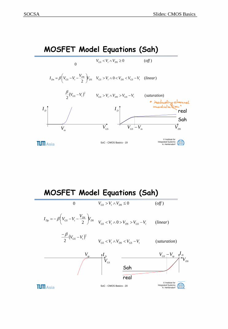
MOSFET Model Equations (Sah)
)(
)(0
)(0
2
2
0
2
saturationVVVVV
linearVVVVV
offVVV
VV
VV
VVI
tGSDStGS
tGSDStGS
DStGS
tGS
DSDS
tGSDn
DSV
DI
tnGSVV
GSV
DI
tnV
Sah
real
© Institute for
Integrated Systems
A. Herkersdorf SoC - CMOS Basics - 20
MOSFET Model Equations (Sah)
DSV
tpGSVV D
I
)(
)(0
)(0
2
2
0
2
saturationVVVVV
linearVVVVV
offVVV
VV
VV
VVI
tGSDStGS
tGSDStGS
DStGS
tGS
DSDS
tGSDp
GSVD
ItpV
Sah
real

SOCSA Slides: CMOS Basics
© Institute for
Integrated Systems
A. Herkersdorf SoC - CMOS Basics - 21
Dimensioning
Oxt
minL
w
L
WK Transconductance: where
Ox
Ox
tK 0
Designer’s Parameter: W
Conflicting Design Goals: Area => W=Lmin
Speed => high W, l=Lmin
=> always use Lmin for digital circuits
Technology Parameters Mobility µn = 1.5 .. 3.5 x µp
Designer uses W to compensate for lower current drive of pMOSFETS
Minimum Feature Size: Lmin
Oxide dielectric/thickness: εox,tox
© Institute for
Integrated Systems
A. Herkersdorf SoC - CMOS Basics - 22
Module outline
Overview
CMOS Device Basics
Static CMOS Logic
Inverter
Logic Gates
Arithmetic in CMOS
Sequential Logic CMOS and FSM design
Power Consumption Of Static CMOS Logic

SOCSA Slides: CMOS Basics
© Institute for
Integrated Systems
A. Herkersdorf SoC - CMOS Basics - 23
Static CMOS Inverter
gnd
A Z
gnd
VDD
VA VZ
D
S
S
P
N
Ip
VDSp
VGSp
VGSn
VDSn A Z
0 1
1 0
© Institute for
Integrated Systems
A. Herkersdorf SoC - CMOS Basics - 24
Static Voltage Transfer Curve (VTC)
gnd
VZ
VA Vtn VDD-|Vtp|
VDD
A Z
0 1
1 0
VDD
VA VZ
D
S
S
P
N
Ip
VDSp
VGSp
VGSn
VDSn
Ip
Vth
off
on
off on N P

SOCSA Slides: CMOS Basics
© Institute for
Integrated Systems
A. Herkersdorf SoC - CMOS Basics - 25
VTC: Logic Levels “0” / “1”
gnd
VZ
VA Vtn VDD-|Vtp|
VDD
A Z
0 1
1 0
VDD
VA VZ
D
S
S
P
N
Ip
VDSp
VGSp
VGSn
VDSn
Vth
off
on
off on N P
© Institute for
Integrated Systems
A. Herkersdorf SoC - CMOS Basics - 26
Dynamic Behaviour VA
t
VZ
t
tpHL tpLH
Propagation delay from input to output No infinitely steep slopes
at input
Capacitive Load at the output needs to be (dis)charged
50% Signal level marks serve as measure hooks
Typical Inverter (65 nm) delay as of today: 24 ps
50%
50%
t
Ip

SOCSA Slides: CMOS Basics
© Institute for
Integrated Systems
A. Herkersdorf SoC - CMOS Basics - 27
Effect of Input Slope on Inv. Delay
VA
t tHL
Transition time of a signal: Time elapsed between 10%
and 90% of swing
Effect on delay: For a falling (rising) input
signal, no output rise (fall) can occur before P (N) switches to on
10%
90% Vdd-
|Vtp|
P still off (Z still low)
P on (Z rising)
|Vtp|
tHL => tpLH Vtn
tLH => tpHL
© Institute for
Integrated Systems
A. Herkersdorf SoC - CMOS Basics - 28
Effect of Capacitance on Inv. Delay
VA
wire
Driving gate
Driven gate(s)
Other wire
A Z
Lumped capacitance
Lumped Capcitance: Input (gate) capacities of next
logic gates
+ Drain capacities
+ Wire capacities 0.13µ: 3-6 fF

SOCSA Slides: CMOS Basics
© Institute for
Integrated Systems
A. Herkersdorf SoC - CMOS Basics - 29
Effect of Capacitance on Inv. Delay
VA
Lumped capacitance
VZ
Vdd
Vdsp
Vgsp
IC
Idp
C
t
VZ
t 50%
tpLH=f(C)=?
Vgsp=-Vdd
Vgsp-Vtp
Vdsp
For a first order analysis we assume the input slope to be infinitely steep …
VA
… and that we operate the FET in its linear region
Vgsp
© Institute for
Integrated Systems
A. Herkersdorf SoC - CMOS Basics - 30
Effect of Capacitance on Inv. Delay
t
t
VZ=VC
50%
Inverter model: on: Resistance
off: open switch
operating in linear region of Sah
Ron,n
C
gnd
Vdd Ron,p
VA

SOCSA Slides: CMOS Basics
© Institute for
Integrated Systems
A. Herkersdorf SoC - CMOS Basics - 31
Effect of Capacitance on Inv. Delay
t
t
VA
VZ
50%
Ron,n
C
gnd
Vdd Ron,p
tpLH=f(C)=?
Inverter model: on: Resistance
off: open switch
operating in linear region of Sah
© Institute for
Integrated Systems
A. Herkersdorf SoC - CMOS Basics - 32
Effect of Capacitance on Inv. Delay
Derivation : 1) Kirchhoff for currents:
2) Capacitor formula:
3) W´s law:
4) Kirchhoff for voltages:
5) Resolve by ∂t:
6) Some math:
0
tV
CI Cdp
0Cdp
II
0,
tV
CR
VC
pon
dsp
0,
t
VC
RVV
C
pon
ddC
C
ddC
ponV
VV
CRt
,
2
1ln,
5.0
0
,
0
CRtVVV
CRt ponp
V
C
ddC
pon
tddp

SOCSA Slides: CMOS Basics
© Institute for
Integrated Systems
A. Herkersdorf SoC - CMOS Basics - 33
Effect of Capacitance on Inv. Delay
21
, lnCRt ponpLH DS
V
DI
Sah
real pon
R,
simple
||||||tpGSpDSp
VVV for
DSp
DSp
tpGSpdp VV
VVI
2
||||1
,tpGSpdp
DSppon VVI
VR
© Institute for
Integrated Systems
A. Herkersdorf SoC - CMOS Basics - 34
Discussion
|| tpddOxpp
pOxloadpLH VVW
LtCt
Increase of Capacitive Load
Oxide thickness
Channel length
abs. threshold voltage
=> Propagation delay increase
... Mobility
Channel width
relative oxide (=k)
Supply Voltage
=>Propagation delay decrease

SOCSA Slides: CMOS Basics
© Institute for
Integrated Systems
A. Herkersdorf SoC - CMOS Basics - 35
Dimensioning II
The threshold voltage is an important parameter.
It’s value must be carefully selected, by technology factors: Channel Doping
Oxide thickness
at design time: choosing a technology that supports
multiple (two) threshold voltages
by introducing a substrate voltage
at run time: by adopting the substrate voltage
to design conditions
gnd
Channel doping
Vbulk S
© Institute for
Integrated Systems
A. Herkersdorf SoC - CMOS Basics - 36
Simple Static CMOS Logic Gates
VDD
gnd
A
B
Z
D
A
B
Z
NAND
NOR Z
Z A
B
A
B
NAND NOR Z A B Z
1 0 0 1
1 0 1 0
1 1 0 0
0 1 1 0

SOCSA Slides: CMOS Basics
© Institute for
Integrated Systems
A. Herkersdorf SoC - CMOS Basics - 37
Generic Model of Static CMOS
VDD
gnd
A1
...
An
Z
C
NAND NOR
© Institute for
Integrated Systems
A. Herkersdorf SoC - CMOS Basics - 38
Why not like this?
VDD
gnd
A
B
Z
OR ?
Drain
Source
Drain
Source VGSp
VGSn
MOSFET Input Characteristic Condition for MOSFET to build up
conducting channel: Vgs > Vt
In figure on the left:
nMOS pulls up Z to VDD – Vtn („bad pull up“)
pMOS pulls down Z to ¦Vtp¦ (bad „pull down“)
Problematic signal levels for next logic stage

SOCSA Slides: CMOS Basics
© Institute for
Integrated Systems
A. Herkersdorf SoC - CMOS Basics - 39
Systematic Static CMOS Logic Design
Example Function: Z=AB+C CMOS always inverts => add
extra inverter: Z=AB+C
VDD
gnd
Z
parallel for OR (C) C
Start at the output and find a way through n-MOSFETS to ground:
serial for AND (AB)
A
B If everything is done right, there will never be a conducting path between Vdd and gnd.
A B
C
Draw the way to Vdd by using the dual n-network and p-MOSFETS
© Institute for
Integrated Systems
A. Herkersdorf SoC - CMOS Basics - 40
References
[1] R. J. Baker et al., CMOS circuit design, layout, and simulation, IEEE Press, 1998. ISBN 0-7803-3416-7
[2] N. H. E. Weste et al., Principles of CMOS VLSI Design, Addison Wesley, 1993. ISBN 0-201-53376-6
[3] SIA, International Technology Roadmap for Semiconductors, http://public.itrs.net/
Picture credits:
www.ibm.com ,www.alternate.de, www.spacedaily.com, www.gifte.de, www.brl.ntt.co.jp, www-imt.unine.ch, allserv.rug.ac.be

SOCSA Slides: CMOS Basics
© Institute for
Integrated Systems
A. Herkersdorf SoC - CMOS Basics - 41
© Institute for
Integrated Systems
A. Herkersdorf SoC - CMOS Basics - 42