Embed Size (px)
Citation preview

University of Massachusetts Amherst University of Massachusetts Amherst
ScholarWorks@UMass Amherst ScholarWorks@UMass Amherst
Open Access Dissertations
9-2011
Clock Generation and Distribution for Enhancing Immunity to Clock Generation and Distribution for Enhancing Immunity to
Power Supply Noise Power Supply Noise
Jinwook Jang University of Massachusetts Amherst
Follow this and additional works at: https://scholarworks.umass.edu/open_access_dissertations
Part of the Electrical and Computer Engineering Commons
Recommended Citation Recommended Citation Jang, Jinwook, "Clock Generation and Distribution for Enhancing Immunity to Power Supply Noise" (2011). Open Access Dissertations. 455. https://scholarworks.umass.edu/open_access_dissertations/455
This Open Access Dissertation is brought to you for free and open access by ScholarWorks@UMass Amherst. It has been accepted for inclusion in Open Access Dissertations by an authorized administrator of ScholarWorks@UMass Amherst. For more information, please contact [email protected].
CLOCK GENERATION AND DISTRIBUTION FOR ENHANCING IMMUNITY TO POWER SUPPLY NOISE
A Dissertation Presented
by
JINWOOK JANG
Submitted to the Graduate School of the University of Massachusetts Amherst in partial fulfillment
of the requirements for the degree of
DOCTOR OF PHILOSOPHY
September 2011
Department of Electrical and Computer Engineering

© Copyright by Jinwook Jang 2011
All Rights Reserved
CLOCK GENERATION AND DISTRIBUTION FOR ENHANCING IMMUNITY
TO POWER SUPPLY NOISE
A Dissertation Presented
by
JINWOOK JANG
Approved as to style and content by: _______________________________________ Wayne Burleson, Chair _______________________________________ Sandip Kundu, Member _______________________________________ Charles Weems, Member _______________________________________ Olivier Franza, Member
____________________________________ Christopher V. Hollot, Department Head Electrical and Computer Engineering

DEDICATION
사랑하는 나의 어머니 아버지께,
그리고 사랑하는 흔주와 소중한 아들 정우에게 바칩니다.

v
ACKNOWLEDGMENTS
First and Foremost I’d like to thank all the professors whose words make up my
dissertation. To say I couldn’t have done this without them is, for once perhaps, not
merely a cliché. Almost as essential was Prof. Wayne Burleson, my advisor. His
continued support and encouragement were invaluable in the process of selecting topics
and shaping my dissertation as well as all other helps I got from him during my M.S and
Ph.D years. I also would like to thank other my committee members, Prof. Kundu, Prof
Weems, and Dr Franza who were enthusiastic about my dissertation through their
precious feedbacks and comments.
I am very grateful to Bill Bowhill and Mandy Pant in Intel, who showed me
various interesting works and guided me to better research during my productive
internship period at Hudson. Also many thanks to Dr. Omid Oliaei who advised me
regarding analog circuit design. Prof. Salthouse, whom I had a great conversation with in
terms of the analog reference generation circuit and the sample and hold circuit, should
not be eliminated from the list of people I want to express my appreciation.
I believe all my friends and students I met in graduate school directly and
indirectly helped create my dissertation, but I’d like to single out my friends, Atul, Nidhi,
Vishak, Sheng, Aniket, Venkatesh, Ibis, and Basab. And finally, my dissertation could
only have been written with the supports of my parents, my wife, Hunju and my son,
Jeong-Woo (especially about his patience when I couldn’t play with him to finish up this
work). I’d like to express my sincere gratitude to all of them
vi
ABSTRACT
CLOCK GENERATION AND DISTRIBUTION FOR ENHANCING IMMUNITY TO POWER SUPPLY NOISE
SEPTEMBER 2011
JINWOOK JANG, B.E., KYUNGHEE UNIVERSITY, KOREA
M.S.E.C.E, UNIVERSITY OF MASSACHUSETTS AMHERST
Ph.D., UNIVERSITY OF MASSACHUSETTS AMHERST
Directed by: Professor Wayne Burleson
Clock generation and distribution are getting difficult due to increased die size
and increased number of cores in a microprocessor. Clock frequencies of microprocessors
have been increased and expected to trend 4GHz in near future. This increased clock
frequency requires to limit the clock skew and jitter to 5~10% of clock frequency, which
is 12.5~25ps. On top of this, non-ideal power supply behavior (supply droops) is
worsening available timing margin to the critical paths.
This dissertation presents three types of interrelated works: 1) analytical modeling
of period jitter of global clock distribution induced by power supply droop, 2) circuit
design of a power supply droop detector with 20mV resolution and 1 cycle latency, and 3)
architectural studies regarding new adaptive clocking architectures which reduce the
worst case period jitter and the worst timing slack.
In the analytical modeling of period jitter in global binary clock tree, period jitter
caused by power supply droop is formulated into recursive expressions based on
propagation delay variation expressions. These recursive expressions are simplified into
non-recursive expressions to pinpoint the location of the worst case period jitter in time
domain. During this process, the physical relationship between the power supply noise
vii
and period jitter is studied extensively in time domain. The resulted analytical
expressions can predict the period jitter in the clock distribution with only 5 ps error
compared to HSPICE simulations. [1] [2] [3]
The study of period jitter in global clock distribution showed that the input period
jitter into the clock distribution can be adjusted to improve the period jitter at the end of
the clock distribution. To achieve input jitter modulation, a very fast supply droop
detector is vital. To address this challenge, a droop detector system is designed based on
a detailed study on high end microprocessor power supply network. The study shows that
the detector system can detect the supply noise with 20mV resolution in only one clock
cycle latency. [4]
My two works are combined to study new adaptive clocking architectures. Two
types of adaptive clocking architectures are studied and the results show both
architectures can improve the worst case slack by 10ps. This can be considered a
significant improvement when it is compared to the traditional worst case based clocking.
viii
TABLE OF CONTENTS
Page ACKNOWLEDGMENTS ...................................................................................................v
ABSTRACT ....................................................................................................................... vi
LIST OF TABLES ............................................................................................................ xii
LIST OF FIGURES ......................................................................................................... xiii
CHAPTER 1. INTRODUCTION ...................................................................................................1
1.1 Motivation ..........................................................................................................1
1.2 Organization .......................................................................................................2
2. OVERVIEW OF CLOCK GENERATION AND DISTIRIBUTION .....................3
2.1 Clock Jitter .........................................................................................................3
2.1.1 Timing Notation ..................................................................................3
2.1.2 Definitions of Clock Jitter ...................................................................4
2.1.2.1 Period Jitter ..........................................................................5
2.1.2.2 Cycle Jitter ...........................................................................6
2.1.2.3 Cycle-to-cycle Jitter .............................................................6
2.1.2.4 Long Term Jitter ..................................................................7
2.1.3 Sources of Jitter ...................................................................................7
2.1.4 Impact of Jitter on Synchronous Systems .........................................10
2.1.4.1 Impact of Jitter on a Simple Sequential Circuit .................12
2.1.4.2 Impact of Jitter on a Pipelined Datapath ............................13
2.2 Clock Architecutre for Multicore Processors ..................................................15
ix
2.2.1 Pentium 4 (180nm) ...........................................................................16
2.2.2 Pentium 4 (90nm) .............................................................................17
2.2.3 Montecito ..........................................................................................18
2.2.4 Dual-core Xeon (65nm) ....................................................................20
2.2.5 Nehalem (45nm) ...............................................................................22
2.3 Summary ..........................................................................................................23
3. CLOCK DISTRIBUTION MODELING ...............................................................24
3.1 Clock Distribution Modeling ...........................................................................25
3.1.1 Global Binary Clock Tree Topology ................................................25
3.1.2 Power Supply Noise and Timing Notation .......................................29
4. SUPPLY NOISE INDUCED PERIOD JITTER IN GLOBAL CLOCK DISTRIBUTION....................................................................................................33
4.1 Recursive Period Jitter Expression ..................................................................33
4. 2 Propagation Delay Sensitivity of Clock Distribution Cells due to Static Supply Noise ..............................................................................................33
4.3 Recursive Period Jitter Expression ..................................................................36
4.3.1 Comparison between HSPICE Simulation and Analytical Expression ......................................................................................37
4.3.1.1 Considerations for Circuit Simulations ..............................37
4.3.1.2 Comparisons between HSPICE and Recursive Expression .....................................................39
4.4 Non-recursive Period Jitter Expression ...........................................................41
4.5 Worst Case Period Jitter ...................................................................................45
4.6 Physical Insight into Period Jitter Induced by Supply Droop ..........................50
4.6.1 Impact of Nonlinear Propagation Delay Sensitivity .........................50
x
4.6.2 Impact of the Number of Clock Stages, K. (or Total Propagation Delay through Clock Distribution, tp_n*K) ...............52
4.6.3 Impact of Clock Driver Sizes, H. ( or Improved Sensitivity) ...........57
4.6.4 Impact of Supply Noise ....................................................................59
4.6.5 Damped Sinusoidal Supply Noise ....................................................60
4.6.6 CPU time Requirements for Circuit Simulations ..............................61
4.7 Case Study: Putting Everything Together for Clock Data Compensation (Active Jitter Mitigation based on VCO Voltage Modulation) ................63
4.8 Conclusion .......................................................................................................68
5. POWER SUPPLY DROP AND ON-DIE DROOP DETECTOR .........................69
5.1 Introduction ......................................................................................................69
5.2 Power Delivery Network .................................................................................71
5.3 Droop Detector System ....................................................................................75
5.4 Simulation Results ...........................................................................................80
5.4.1 Metastability in the Arbiter ...............................................................80
5.4.2 Monte Carlo Yield Analysis of A Droop Detector Core (DDC) .................................................83
5.5 Droop Detector Test Chip ................................................................................88
5.5.1 Bandgap Reference ...........................................................................89
5.5.2. Voltage Reference Generator ...........................................................93
5.5.3 Voltage Controlled Ring Oscillator and Clock Distribution .............96
5.5.4 Current DAC .....................................................................................98
5.5.5 Full Chip Layout and Simulation Results. ......................................101
5.6 Conclusion .....................................................................................................103
6. ADAPTIVE CLOCKING ARCHITECTURE ....................................................104
xi
6.1 PLL Design Procedure ...................................................................................104
6.1.1 Design Specification of an Adaptive PLL ......................................106
6.2. Metrics for the Performance of an Adaptive Clocking Architecture ............112
6.2.1 Locking Behavior ............................................................................112
6.2.2 Worst Case Period Jitter and Worst Timing Slack .........................114
6.3 Impact of Feedback Source Selection and Supply Droop Amplitude ...........115
6.4 A New Adaptive Clocking System based on a Mixed Signal Approach .......118
6.5 A New Adaptive Clocking System based on Pure Analog Approach ...........124
6.6 Conclusion .....................................................................................................125
7. CONCLUSIONS AND FUTURE WORK ..........................................................126
7.1 Conclusions ....................................................................................................126
7.2 Future Work ...................................................................................................127
APPENDICES A. MINIMUM REQUIRED ODER FOR APPROXIMATION ..............................128
B. IBM 45nm SOI TEST CHIP POST SILICON MREASUREMENT RESULTS .......................................................................131
BIBLIOGRAPHY ............................................................................................................150
xii
LIST OF TABLES
Table Page
2.1. Four levels of clock distribution system for Montecito .........................................19
3.1. Clock driver sizes and interconnect parameters .....................................................29
4.1. Curve-fitted coefficients for three different clock distribution options (VDD=1.1V, 2Vn=0.055, Temp=80˚) ................................................................35
4.2. CPU time comparison for WPJ search ...................................................................62
6.1. PLL design parameter summaries ........................................................................110
A.1. Transistor parameters from [35] ..........................................................................128
B.1. Test chip measurement equipments .....................................................................133
B.2. Pin names and function descriptions of DC pads ................................................134
B.3. Pin names and function descriptions of AC pads. ...............................................135
xiii
LIST OF FIGURES
Figure Page
2.1. Timing parameters: period, width, rise/fall time .....................................................4
2.2. Clock signal uncertainties: skew and jitter ..............................................................4
2.3. Different types of jitter: period, cycle, cycle-to-cycle, and long term jitter ............5
2.4. Sources of jitter in a synchronous system ................................................................8
2.5. Power supply system with multiple stages [15] .......................................................9
2.6. Simulated voltage droops [15] .................................................................................9
2.7. A simple sequential circuit to study the impact of jitter on an edge triggered system ...............................................................................................11
2.8. Pipelined datapath to study the impact of skew and jitter on an edge triggered system ...............................................................................................11
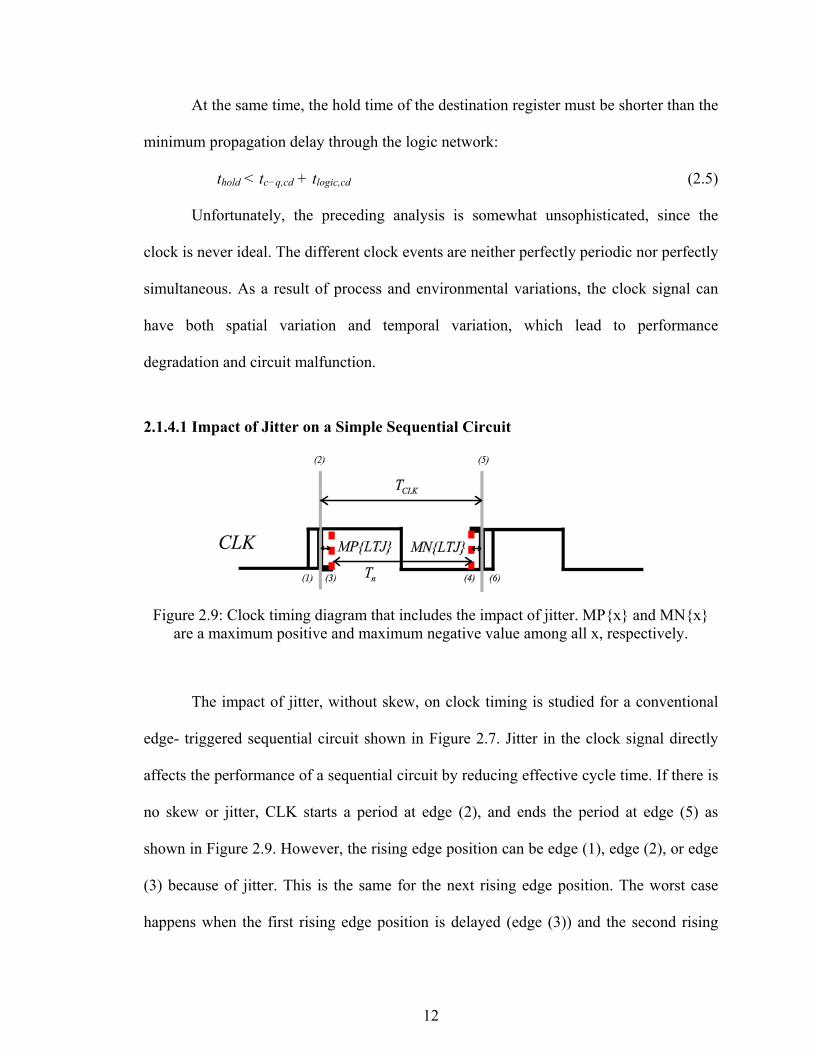
2.9. Clock timing diagram that includes the impact of jitter. MPx and MNx are a maximum positive and maximum negative value among all x, respectively. ............................................................................................12
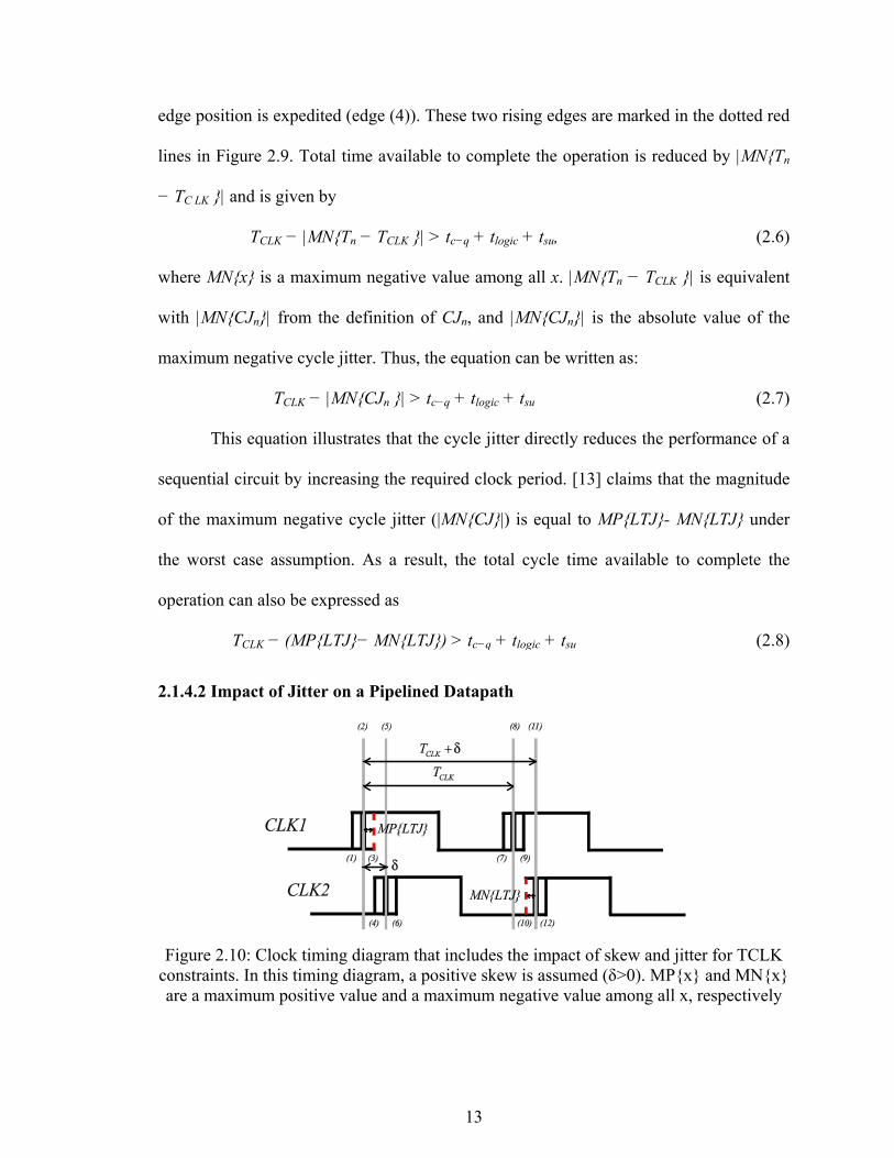
2.10. Clock timing diagram that includes the impact of skew and jitter for TCLK constraints. In this timing diagram, a positive skew is assumed (δ>0). MPx and MNx are a maximum positive value and a maximum negative value among all x, respectively ........................................13
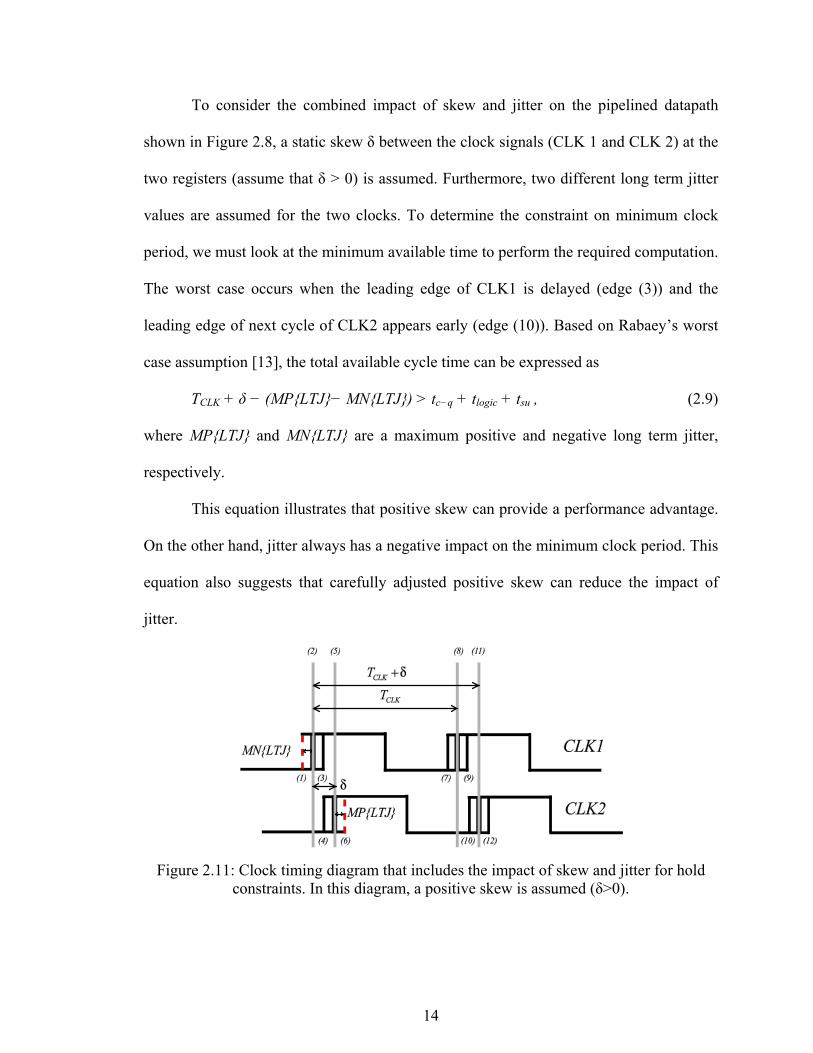
2.11. Clock timing diagram that includes the impact of skew and jitter for hold constraints. In this diagram, a positive skew is assumed (δ>0). ......................14
2.12. High level clock system architecture for Pentium 4 [6] ........................................16
2.13. Pentium 4 (180nm) global clock distribution [6] (a)Triple-spine clock distribution, (b)Binary distribution tree with the three clock spines ...............17
2.14. Pentium 4 (90nm) global clock spines [7] .............................................................17
2.15. Pentium 4 (90nm) - Global clock grid topology with grid drivers in stripes. ........18
2.16. Montecito (90nm) clock system architecture [8] ...................................................19
2.17. Montecito VFC response to supply droop .............................................................20
xiv
2.18. Clock distribution topology comparison (Montecito, Xeon(90nm), and Xeon (65nm)) [9] .............................................................................................21
2.19. 65nm Xeon clock distribution and spines [9] ........................................................21
2.20. Dual-core Xeon core and un-core grid tiles ...........................................................22
2.21. Adaptive analog frequency/supply tracking [10] ...................................................23
3.1. Spine based global binary clock tree [30] ..............................................................27
3.2. Clock tree topology assumption.............................................................................27
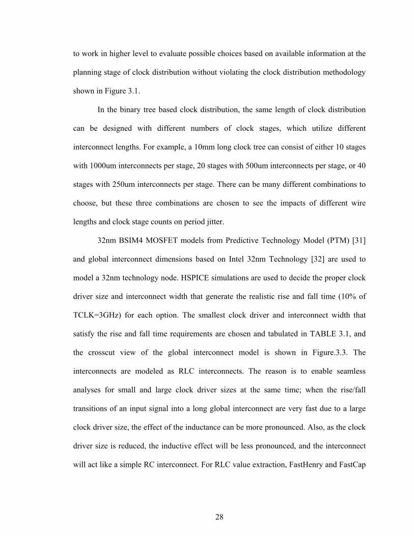
3.3. Crosscut view of global interconnect structures ....................................................29
3.4. Period jitter comparison with damped and undamped supply noise assumptions for a given clock distribution. The worst case period jitter values are almost identical in both cases. ........................................................31
3.5. Timing notations for non-ideal clock and power supply noise assumptions .........32
4.1. Power supply sensitivity test for Option 1 .............................................................34
4.2. One segment of clock tree distribution cells for sensitivity tests ...........................34
4.3. Block diagram representation of the recursive period jitter ...................................37
4.4. An example of ineffective simulation ....................................................................38
4.5. Simulation methodology to cover different phase relationships ............................39
4.6. Period jitter comparisons between HSPICE simulations and recursive period jitter expression, (4.6) ...........................................................................40
4.7. Shmoo plot of supply noise amplitude versus supply noise frequency for approximation accuracy tests with tolerance of 1ps. The left side of each line shows that the error between tn,K
(nr) and tn,K(r) is less than the
given tolerance. The shaded region has to be at the left side of each line to avoid possible approximation errors for the first droop. ......................43
4.8. Period jitter comparisons among HSPICE simulations, recursive period jitter expression, and non-recursive period jitter expression (Option 2), ........44
4.9. Block diagram explanation of simplified non-recursive expression. .....................47
4.10. Error (ps) between the analytically found WPJ based on (15) and PJ(r)
n,K(t)and the numerically searched WPJ based on PJ(r)n,K(t) .....................49
4.11. Graphical illustration of a plotting style in this section .........................................50
xv
4.12. Graphical explanation of the worst case period jitter appearance around 270°. (a) the nth leading edge arrives around 270°, (b) the nth leading edge arrives around 360°. ................................................................................52
4.13. Impact of the number of clock stages (K) on the worst case period jitter .............53
4.14. Impact of increased clock stages (K) on the worst case period jitter. Worsening of worst case period jitter. Red and blue markers represent nth and n+1th leading edges, respectively. (a) K=20, (b) K=30 .......................54
4.15. Impact of increased clock stages (K) on the worst case period jitter. Diminishing return of the worst case period jitter. Red and blue markers represent nth and n+1th leading edges, respectively. (a) K=53, (b) K=63 ...........................................................................................................55
4.16. Impact of the number of clock stages with comparable total propagation delays. The nominal propagation delays of all options are around 322 ps. .....................................................................................................................56
4.17. Impact of clock driver sizes, H, on the WPJ. (based on Option 2) ........................57
4.18. Sensitivity comparisons with different clock driver sizes (tpLH(Vn) only). (a) shows the full sensitivity (aV2
n +bVn+tpLHN), and (b) shows only the supply noise sensitivity part without the nominal delay (aV2
n+bVn). ..............57
4.19. Comparisons between the impact of the supply sensitive portion and the nominal propagation delay changes. ................................................................59
4.20. Impact of supply noise on the WPJ (based on Option 2) .......................................59
4.21. Impact of different damping factors on period jitter (based on Option 2) .............61
4. 22. Period jitter simulation with supply noise modulated VCO and clock distribution .......................................................................................................64
4.23. Period jitter simulation results with different initial phase assumptions for an adaptive PLL. ..............................................................................................65
4.24. Clock Data Compensation example .......................................................................66
5.1. Power delivery model matched to Nehalem impedance profile ............................72
5.2. Power supply network impedance profiles of Figure 5.1 and Nehalem ................72
5.3. Simulated voltage droop based on three different on-die decoupling capacitor assumptions. .....................................................................................73
5.4. Droop detector system (Calibration controls for each DDC is omitted for simplification) ..................................................................................................75
xvi
5.5. Droop detector core ................................................................................................76
5.6. Simulated waveform of a droop detector core: Near metastable state. ..................78
5.7. Metastable transitions of the arbiter output. ..........................................................80
5.8. MTBF of an arbiter circuit. (N=10 and 100, D = 0.5, 0.6, and 07) .......................82
5.9. Dual DDC structure for improved MBTF. ............................................................82
5.10. CDF of propagation delay of one subcircuit in Figure 5.5. ...................................85
5.11. +3 sigma point comparisons with different sample counts ....................................85
5.12. Impact of calibration on a DDC with different temperature assumptions (Temp = 40C, 60C, and 80C) ..........................................................................87
5.13. Layout of droop detector system. (Supply noise generation circuit is not shown) ..............................................................................................................88
5.14. Simplified bandgap reference design. ....................................................................89
5.15. Layout of bandgap reference design. .....................................................................90
5.16. Bandgap output voltage variation due to temperature at TT corner. .....................91
5.17. Impact of process variation on the output of bandgap reference circuit. ...............92
5.18. Current bias and a simple current mirror loaded op-amp. .....................................93
5.19. Resister ladder based reference generation circuit. ................................................93
5.20. Voltage reference generator stability (Phase margin 58.21 (deg) @135.17Mhz) ..................................................................................................94
5.21. Bandwidth, Phase margin, and Vout......................................................................95
5.22. Layout of reference generation circuit. ..................................................................95
5.23. Ring oscillator and clock distribution schematic. ..................................................97
5.24. Ring oscillator and clock distribution layout. (95x160). .......................................97
5.25. Clock frequency and duty cycle change over different control voltages. ..............98
5.26. Zoomed in version of full chip layout 2384x690 um2. ..........................................99
5.27. Current mode DAC. .............................................................................................100
xvii
5.28. Layout of Current mode DAC (30x39 um2) ........................................................100
5.29. Full chip layout of the droop detector system ......................................................101
5.30. Comparison between noisy supply and reconstructed supply voltage based on droop detector system outputs (Post layout simulation result). ................102
6.1. Nehalem PLL loop ...............................................................................................104
6.2. PLL locations of a Quad-Core Opteron Processor. .............................................105
6.3. Nehalem PLL architecture. [55] ..........................................................................106
6.4. Simulink modeling of Phase Frequency Detector (PFD) ....................................107
6.5. Simulink modeling of charge pump and lead lag loop filter [56]. .......................108
6.6. Differential buffer delay stage with symmetric loads [57]. .................................108
6.7. Simulink modeling of a clock distribution cell in Section 3. ...............................110
6.8. Simulink modeling of Clock distribution Option 1 in Section 3 and 4. ..............111
6.9. Simulink-based adaptive PLL. Droop detection and adaptive delay generation block is marked with a blue square. .............................................111
6.10. Simulink modeling of an In-Lock detector ..........................................................112
6.11. Simulink simulation result of PLL locking behavior. ..........................................113
6.12. In-Lock indication behavior onset of a severe supply noise droop .....................114
6.13. Clock Data Compensation example .....................................................................115
6.14. Two different feedback path selection options ....................................................116
6.15. Comparison of two different design choices (clock distribution=Option1) ........116
6.16. Impact of supply noise on PLL lock status and Data path slack. ........................117
6.17. Simulink model of a droop detector. Voltage reference and droop detector cores are modeled as edge triggered compare blocks. ...................................119
6.18. Simulink model of droop detection and delay adjustment block marked as dd_vcdl in Figure 6.9 .....................................................................................120
6.19. Operation of droop detection and delay adjustment block. .................................121
xviii
6.20. Shmoo plots of the worst case period jitter (WPJ), worst case timing slack (WTS), and lock-out period (LOP). (The actual values are added on the top of the Shmoo plot). The pink colored cells present a failure when compared to a given specification. .......................................................122
6.21. Conceptual schematic of analog delay adjustment circuit. ..................................124
6.22. Simulink model of a continuous time and fully analog delay adjustment circuit. ............................................................................................................125
A.1. Error between the original propagation delay expression and 5th order Taylor polynomial ..........................................................................................129
A.2. Comparisons of approximations error to (A.1). ...................................................130
B.1. Test bench with probe station and measurement equipments ..............................131
B.2. Test die mounted on probe-station (Cascade Microtech model 12 microwave probe fixture) ...............................................................................132
B.3. Example of test probe mounted on the probe station ...........................................133
B.4. Full chip layout of the droop detector system (2300 x 800 um2) .........................133
B.5. Full chip layout of the droop detector system ......................................................133
B.6. Bandgap reference voltage ...................................................................................137
B.7. Op-Amp based reference generation circuit. .......................................................138
B.8. Digital section supply IR drop. ............................................................................138
B.9. VDDD metal wire with meshed connection to an AC pad ..................................139
B.10. Concept of supply noise generation and measurement ........................................139
B.11. 40MHz sinusoidal supply noise ...........................................................................141
B.12. 60MHz sinusoidal supply noise ...........................................................................141
B.13. 80MHz sinusoidal noise .......................................................................................142
B.14. Current steering DAC ..........................................................................................143
B.15. Measured frequency of ring oscillator. ................................................................144
B.16. Clock frequency change based on ring oscillator supply voltage change ...........145
B.17. Droop detector output when VDDD >>VREF. ...................................................146
xix
B.18. Droop detector output when the lowest VDDD voltage cross VREF for a certain period (P1). .........................................................................................146
B.19. Droop detector output when the lowest VDDD voltage cross VREF for a certain period (P2). P2>P1. ............................................................................147
B.20. Droop detector output when the lowest VDDD voltage cross VREF for a certain period (P3). P3>P2>P1. .....................................................................147
B.21. Droop detector output when the highest VDD voltage is below the reference voltage. ...........................................................................................148
1
CHAPTER 1
INTRODUCTION
1.1 Motivation
Primary objectives of this work are to understand clock jitter in global clock
distribution trees, and to mitigate an impact of clock jitter on performance of advanced
microprocessors in global clock distribution and clock generation. International
Technology Roadmap for Semiconductors (ITRS) [5] predicted 10GHz/3GHz clock rates
for local and global clock signals in 2010, respectively. The global clock frequency target
(3GHz) has been already achieved, and it will increase to over 4GHz in the near future.
Clocking architecture for the most advanced multi-core microprocessor must be
designed to withstand contingent clock skew and jitter specifications. However, the
sources of clock uncertainty such as supply voltage droop, process variation, and
temperature variation become more pronounced in deep sub-micron technology. Over the
last decade, clock architects responded to the challenges with spine based clock
distributions, recombined global clock nodes, and dynamic frequency scaling [6] [7] [8]
[9] [10].
My dissertation is driven by the needs of mitigating and utilizing clock
uncertainties in clocking systems of advanced multi-core microprocessors with focuses
on: 1) understanding and modeling clock jitter in global clock distribution due to the
supply noise injected to clock drivers, 2) designing a droop detection system which will
aid an adaptive clocking system, 3) mitigating clock jitter based on a adaptive clocking
system.
2
1.2 Organization
My dissertation is organized as follows. Chapter 2 presents a general explanation
about clock jitter and a chronicle review of clocking architectures. In Chapter 3, a global
binary clock tree topology and power supply noise model are explained, and these models
are used throughout this work. Analytical modeling of period jitter is presented in
Chapter 4. Chapter 5 presents a design of a supply droop detector system. Finally,
adaptive clock generation based on low latency feedback from the droop detector is
proposed in Chapter 6.
3
CHAPTER 2
OVERVIEW OF CLOCK GENERATION AND DISTIRIBUTION
2.1 Clock Jitter
High-performance digital systems require synchronization techniques to maintain
high clock rates and reliable data transfers. To get benefits from the faster clock
frequency, timing uncertainty of the clock signal must be kept to a constant ratio (5~10%)
of the clock period. This implies the jitter/skew must be maintained under 25ps with a
4GHz clock frequency assumption. In the past, most of the jitter came from clock
generation circuitry, generally an on-chip phase-locked loop (PLL) that multiplies the
off-chip clock reference to provide the core clock frequency. However, PLL jitter has
scaled well with technology, while the jitter in the clock distribution has not. Since a
global clock is repeated in several stages by using repeaters experiencing noisy VDD and
GND, jitter in the distribution network is the dominant source of clock jitter for today’s
high-performance microprocessors [11].
2.1.1 Timing Notation
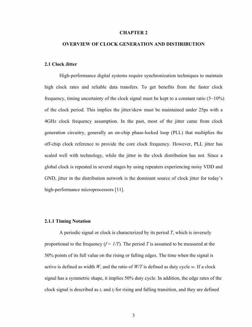
A periodic signal or clock is characterized by its period T, which is inversely
proportional to the frequency (f = 1/T). The period T is assumed to be measured at the
50% points of its full value on the rising or falling edges. The time when the signal is
active is defined as width W, and the ratio of W/T is defined as duty cycle w. If a clock
signal has a symmetric shape, it implies 50% duty cycle. In addition, the edge rates of the
clock signal is described as tr and tf for rising and falling transition, and they are defined
4
between the 10% and 90% points of the signal. Response time for a low to high output
transition is defined as tpLH, while the response time for a high to low output transition is
defined as tpHL. These basic timing parameters are illustrated in Figure 2.1.
Figure 2.1: Timing parameters: period, width, rise/fall time
2.1.2 Definitions of Clock Jitter
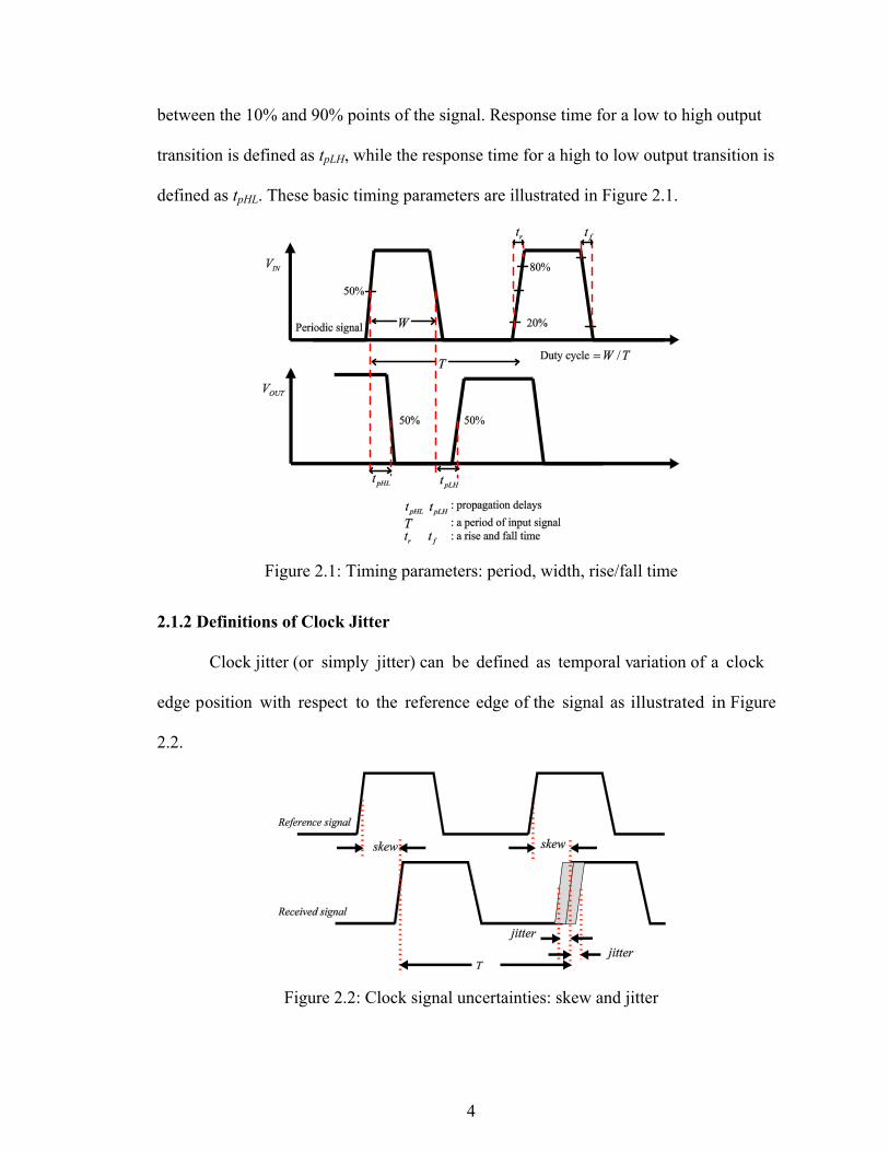
Clock jitter (or simply jitter) can be defined as temporal variation of a clock
edge position with respect to the reference edge of the signal as illustrated in Figure
2.2.
Figure 2.2: Clock signal uncertainties: skew and jitter
5
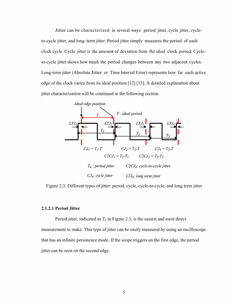
Jitter can be characterized in several ways: period jitter, cycle jitter, cycle-
to-cycle jitter, and long- term jitter. Period jitter simply measures the period of each
clock cycle. Cycle jitter is the amount of deviation from the ideal clock period. Cycle-
to-cycle jitter shows how much the period changes between any two adjacent cycles.
Long-term jitter (Absolute Jitter or Time Interval Error) represents how far each active
edge of the clock varies from its ideal position [12] [13]. A detailed explanation about
jitter characterization will be continued in the following section.
Figure 2.3: Different types of jitter: period, cycle, cycle-to-cycle, and long term jitter
2.1.2.1 Period Jitter
Period jitter, indicated as Tn in Figure 2.3, is the easiest and most direct
measurement to make. This type of jitter can be easily measured by using an oscilloscope
that has an infinite persistence mode. If the scope triggers on the first edge, the period
jitter can be seen on the second edge.
6
The period jitter is simple to be measured, but it serves as a baseline to measure
other types of jitter. In the following section, cycle jitter, cycle-to-cycle jitter and long-
term jitter will be formulated in terms of the period jitter.
2.1.2.2 Cycle Jitter
The cycle jitter in Figure 2.3 is the deviation of clock period from a nominal
(ideal) clock period, and it can be formulated as follows.
CJn = Tn − T , (2.1)
where T is a nominal (ideal) clock period, and Tn is the nth period. If CJn > 0, this means
expansion of the nth clock period. Conversely, if CJn < 0, this means compression of the
nth clock period.
Period jitter and cycle jitter directly impact on the performance of sequential logic,
because a negative cycle jitter reduces the effective cycle time of critical paths.
Consequently, these are the greatest concerns for high performance microprocessors.
2.1.2.3 Cycle-to-cycle Jitter
Cycle-to-cycle jitter measures how much the clock period changes between any
two adjacent cycles as shown in Figure 2.3, and it can be calculated by subtracting two
consecutive period jitter values.
C2CJn = Tn+1 − Tn (2.2)
Because cycle-to-cycle jitter shows the instantaneous dynamics of clock signal, it
can be important to inter-core communication circuits for a multi-core SoC. The
communication circuits can send and receive data without a common reference clock
signal, or it can forward a clock signal to other communication circuits. This process
7
usually requires a PLL based clock recovery circuit to correctly synchronize two different
clock domains. Severe cycle-to-cycle jitter can corrupt the locking behavior of the
recovery circuit.
2.1.2.4 Long Term Jitter
Long-term jitter (or absolute jitter or Time Interval Error) is shown in Figure 2.3,
and it can be defined as a summation of cycle jitter over n cycles.
1
n
n kk
LTJ CJ=
=
(2.3)
Long-term jitter is defined as the deviation of a clock edge from the ideal one
over more than one clock cycle. While period jitter and cycle jitter are defined for one
clock cycle, long term jitter is defined for multiple clock cycles.
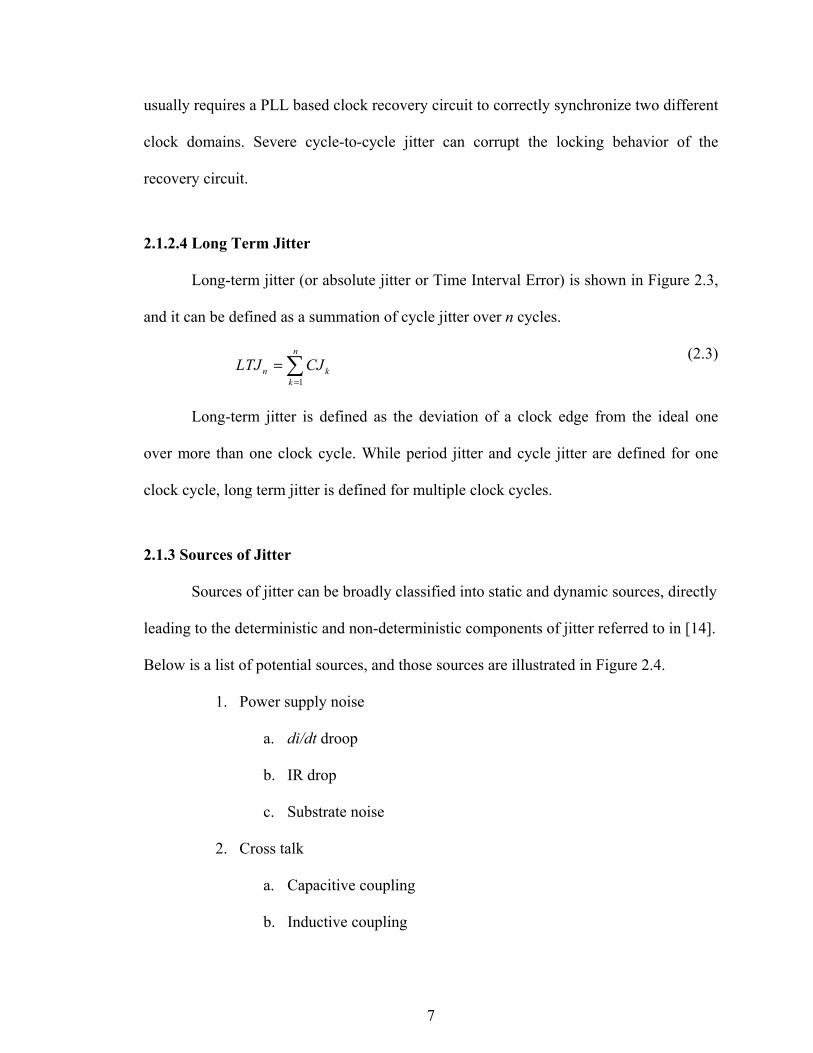
2.1.3 Sources of Jitter
Sources of jitter can be broadly classified into static and dynamic sources, directly
leading to the deterministic and non-deterministic components of jitter referred to in [14].
Below is a list of potential sources, and those sources are illustrated in Figure 2.4.
1. Power supply noise
a. di/dt droop
b. IR drop
c. Substrate noise
2. Cross talk
a. Capacitive coupling
b. Inductive coupling
8
3. Clock generation
4. Others
a. Thermal noise
b. Intra die temperature variation
Figure 2.4: Sources of jitter in a synchronous system
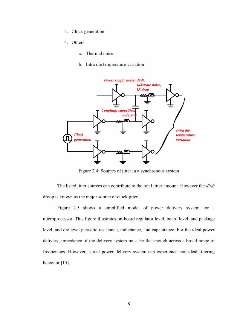
The listed jitter sources can contribute to the total jitter amount. However the di/dt
droop is known as the major source of clock jitter.
Figure 2.5 shows a simplified model of power delivery system for a
microprocessor. This figure illustrates on-board regulator level, board level, and package
level, and die level parasitic resistance, inductance, and capacitance. For the ideal power
delivery, impedance of the delivery system must be flat enough across a broad range of
frequencies. However, a real power delivery system can experience non-ideal filtering
behavior [15].
9
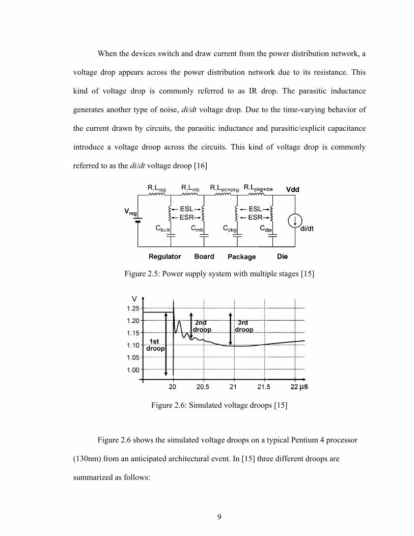
When the devices switch and draw current from the power distribution network, a
voltage drop appears across the power distribution network due to its resistance. This
kind of voltage drop is commonly referred to as IR drop. The parasitic inductance
generates another type of noise, di/dt voltage drop. Due to the time-varying behavior of
the current drawn by circuits, the parasitic inductance and parasitic/explicit capacitance
introduce a voltage droop across the circuits. This kind of voltage drop is commonly
referred to as the di/dt voltage droop [16]
Figure 2.5: Power supply system with multiple stages [15]
Figure 2.6: Simulated voltage droops [15]
Figure 2.6 shows the simulated voltage droops on a typical Pentium 4 processor
(130nm) from an anticipated architectural event. In [15] three different droops are
summarized as follows:

10
1. First droop
a. Source: package inductance and on-die capacitance
b. Duration: a few nanoseconds
2. Second droop
a. Source: motherboard and package decoupling
b. Duration: a few hundred nanoseconds
3. Third droop
a. Source: bulk capacitors
b. Duration: a few microseconds
The second and third droop can be mitigated by utilizing high quality decoupling
capacitors and carefully designed motherboards and packages. However, the first droop
cannot be mitigated by utilizing the same method. This first droop is known to be a
major source of jitter in cutting-edge microprocessors.
2.1.4 Impact of Jitter on Synchronous Systems
Figure 2.7 and Figure 2.8 illustrate two basic structures of synchronous systems: a
simple sequential circuit and a pipelined datapath. The following timing parameters are
assumed for the two types of sequential circuits:
• The contamination or minimum delay (tc−q,cd) and the maximum
propagation delay of a register (tc−q).
• The setup (tsu) and hold times (thold) for a register.
• The contamination delay (tlogic,cd) and the maximum delay (tlogic) of a
combinational logic.
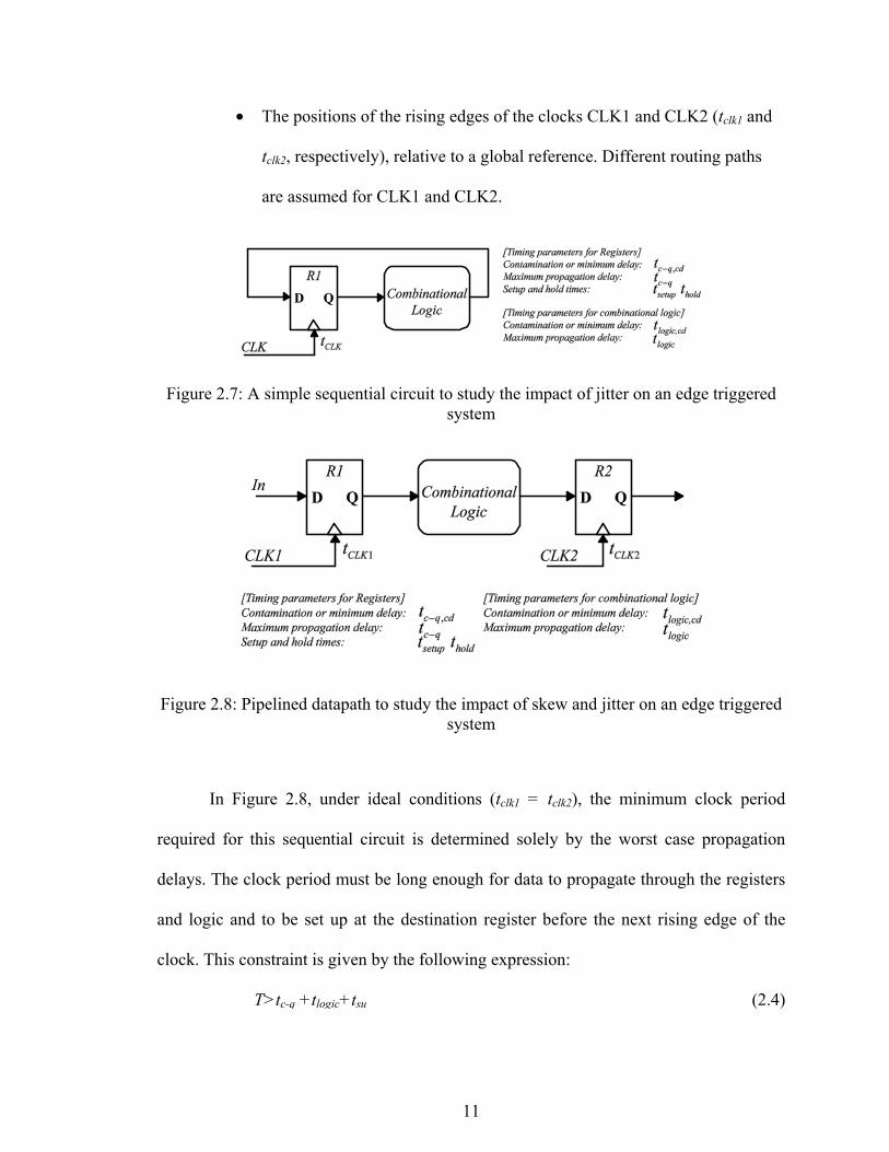
11
• The positions of the rising edges of the clocks CLK1 and CLK2 (tclk1 and
tclk2, respectively), relative to a global reference. Different routing paths
are assumed for CLK1 and CLK2.
Figure 2.7: A simple sequential circuit to study the impact of jitter on an edge triggered system
Figure 2.8: Pipelined datapath to study the impact of skew and jitter on an edge triggered system
In Figure 2.8, under ideal conditions (tclk1 = tclk2), the minimum clock period
required for this sequential circuit is determined solely by the worst case propagation
delays. The clock period must be long enough for data to propagate through the registers
and logic and to be set up at the destination register before the next rising edge of the
clock. This constraint is given by the following expression:
T>tc-q +tlogic+tsu (2.4)
12
At the same time, the hold time of the destination register must be shorter than the
minimum propagation delay through the logic network:
thold < tc−q,cd + tlogic,cd (2.5)
Unfortunately, the preceding analysis is somewhat unsophisticated, since the
clock is never ideal. The different clock events are neither perfectly periodic nor perfectly
simultaneous. As a result of process and environmental variations, the clock signal can
have both spatial variation and temporal variation, which lead to performance
degradation and circuit malfunction.
2.1.4.1 Impact of Jitter on a Simple Sequential Circuit
Figure 2.9: Clock timing diagram that includes the impact of jitter. MPx and MNx are a maximum positive and maximum negative value among all x, respectively.
The impact of jitter, without skew, on clock timing is studied for a conventional
edge- triggered sequential circuit shown in Figure 2.7. Jitter in the clock signal directly
affects the performance of a sequential circuit by reducing effective cycle time. If there is
no skew or jitter, CLK starts a period at edge (2), and ends the period at edge (5) as
shown in Figure 2.9. However, the rising edge position can be edge (1), edge (2), or edge
(3) because of jitter. This is the same for the next rising edge position. The worst case
happens when the first rising edge position is delayed (edge (3)) and the second rising
13
edge position is expedited (edge (4)). These two rising edges are marked in the dotted red
lines in Figure 2.9. Total time available to complete the operation is reduced by |MNTn
− TC LK | and is given by
TCLK − |MNTn − TCLK | > tc−q + tlogic + tsu, (2.6)
where MNx is a maximum negative value among all x. |MNTn − TCLK | is equivalent
with |MNCJn| from the definition of CJn, and |MNCJn| is the absolute value of the
maximum negative cycle jitter. Thus, the equation can be written as:
TCLK − |MNCJn | > tc−q + tlogic + tsu (2.7)
This equation illustrates that the cycle jitter directly reduces the performance of a
sequential circuit by increasing the required clock period. [13] claims that the magnitude
of the maximum negative cycle jitter (|MNCJ|) is equal to MPLTJ- MNLTJ under
the worst case assumption. As a result, the total cycle time available to complete the
operation can also be expressed as
TCLK − (MPLTJ− MNLTJ) > tc−q + tlogic + tsu (2.8)
2.1.4.2 Impact of Jitter on a Pipelined Datapath
Figure 2.10: Clock timing diagram that includes the impact of skew and jitter for TCLK constraints. In this timing diagram, a positive skew is assumed (δ>0). MPx and MNx are a maximum positive value and a maximum negative value among all x, respectively
14
To consider the combined impact of skew and jitter on the pipelined datapath
shown in Figure 2.8, a static skew δ between the clock signals (CLK 1 and CLK 2) at the
two registers (assume that δ > 0) is assumed. Furthermore, two different long term jitter
values are assumed for the two clocks. To determine the constraint on minimum clock
period, we must look at the minimum available time to perform the required computation.
The worst case occurs when the leading edge of CLK1 is delayed (edge (3)) and the
leading edge of next cycle of CLK2 appears early (edge (10)). Based on Rabaey’s worst
case assumption [13], the total available cycle time can be expressed as
TCLK + δ − (MPLTJ− MNLTJ) > tc−q + tlogic + tsu , (2.9)
where MPLTJ and MNLTJ are a maximum positive and negative long term jitter,
respectively.
This equation illustrates that positive skew can provide a performance advantage.
On the other hand, jitter always has a negative impact on the minimum clock period. This
equation also suggests that carefully adjusted positive skew can reduce the impact of
jitter.
Figure 2.11: Clock timing diagram that includes the impact of skew and jitter for hold constraints. In this diagram, a positive skew is assumed (δ>0).
15
To formulate the minimum delay constraint, consider the case in which the
leading edge of the CLK1 cycle arrives early (edge (1)), and the leading edge of CLK2
cycle arrives late (edge (6)) as shown in Figure 2.11. The separation between edges (1)
and (6) should be smaller than the minimum delay through the network. This results in
δ + thold + (MPLTJ− MNLTJ) < tc−q,cd + tlogic,cd (2.10)
or
δ < tc−q,cd + tlogic,cd − thold − (MPLTJ− MNLTJ) (2.11)
with Rabaey’s worst case assumption. This relation indicates that the acceptable skew
amount is reduced because of the jitter of two signals.
2.2 Clock Architecutre for Multicore Processors
As die size grows and CMOS feature size reduces, advanced microprocessors can
afford more than 1 core. Sun UltraSPARC T2 utilizes 8 SPARC cores [17], and Intel’s
Nehalem utilizes four cores [18] [19] [10]. Multicore microprocessors are also required to
meet several design goals:
• Independent supply voltage and clock frequency domain per core • Dynamic supply voltage and clock frequency scaling • Clock Data Compensation [15] • Reliable clock domain crossing
Due to these complicated design requirements, clock architecture started to evolve
from a simple H-tree based architecture [11] to highly sophisticated one. In the following
sections, recent clock generation and distribution architectures are reviewed.
16
2.2.1 Pentium 4 (180nm)
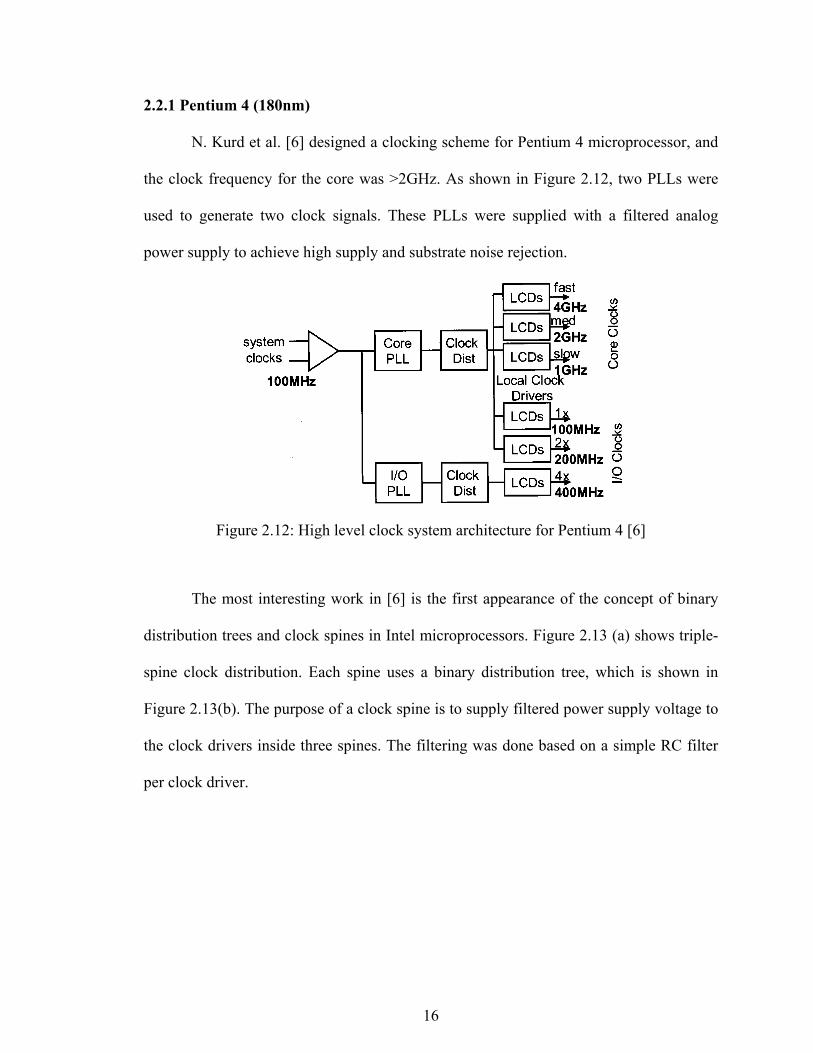
N. Kurd et al. [6] designed a clocking scheme for Pentium 4 microprocessor, and
the clock frequency for the core was >2GHz. As shown in Figure 2.12, two PLLs were
used to generate two clock signals. These PLLs were supplied with a filtered analog
power supply to achieve high supply and substrate noise rejection.
Figure 2.12: High level clock system architecture for Pentium 4 [6]
The most interesting work in [6] is the first appearance of the concept of binary
distribution trees and clock spines in Intel microprocessors. Figure 2.13 (a) shows triple-
spine clock distribution. Each spine uses a binary distribution tree, which is shown in
Figure 2.13(b). The purpose of a clock spine is to supply filtered power supply voltage to
the clock drivers inside three spines. The filtering was done based on a simple RC filter
per clock driver.
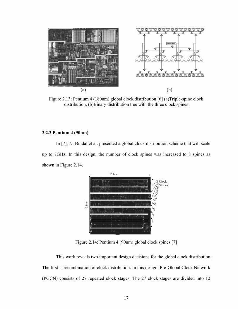
17
(a) (b)
Figure 2.13: Pentium 4 (180nm) global clock distribution [6] (a)Triple-spine clock distribution, (b)Binary distribution tree with the three clock spines
2.2.2 Pentium 4 (90nm)
In [7], N. Bindal et al. presented a global clock distribution scheme that will scale
up to 7GHz. In this design, the number of clock spines was increased to 8 spines as
shown in Figure 2.14.
Figure 2.14: Pentium 4 (90nm) global clock spines [7]
This work reveals two important design decisions for the global clock distribution.
The first is recombination of clock distribution. In this design, Pre-Global Clock Network
(PGCN) consists of 27 repeated clock stages. The 27 clock stages are divided into 12
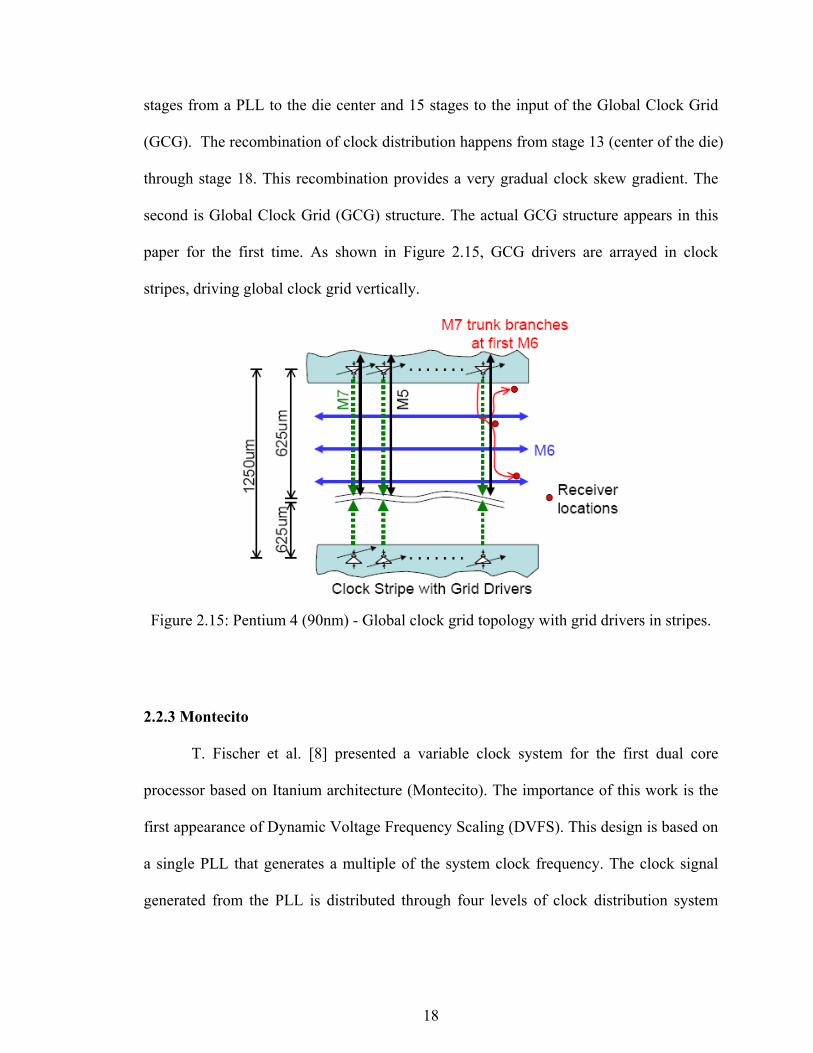
18
stages from a PLL to the die center and 15 stages to the input of the Global Clock Grid
(GCG). The recombination of clock distribution happens from stage 13 (center of the die)
through stage 18. This recombination provides a very gradual clock skew gradient. The
second is Global Clock Grid (GCG) structure. The actual GCG structure appears in this
paper for the first time. As shown in Figure 2.15, GCG drivers are arrayed in clock
stripes, driving global clock grid vertically.
Figure 2.15: Pentium 4 (90nm) - Global clock grid topology with grid drivers in stripes.
2.2.3 Montecito
T. Fischer et al. [8] presented a variable clock system for the first dual core
processor based on Itanium architecture (Montecito). The importance of this work is the
first appearance of Dynamic Voltage Frequency Scaling (DVFS). This design is based on
a single PLL that generates a multiple of the system clock frequency. The clock signal
generated from the PLL is distributed through four levels of clock distribution system
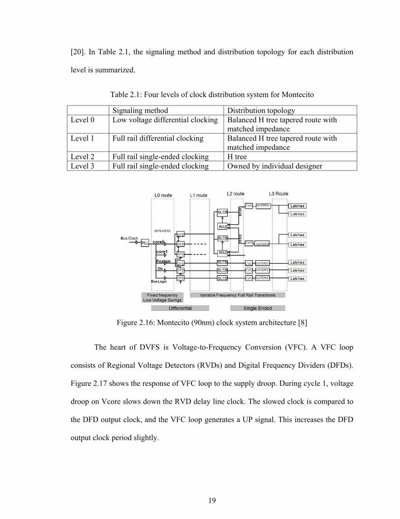
19
[20]. In Table 2.1, the signaling method and distribution topology for each distribution
level is summarized.
Table 2.1: Four levels of clock distribution system for Montecito
Signaling method Distribution topology Level 0 Low voltage differential clocking Balanced H tree tapered route with
matched impedance Level 1 Full rail differential clocking Balanced H tree tapered route with
matched impedance Level 2 Full rail single-ended clocking H tree Level 3 Full rail single-ended clocking Owned by individual designer
Figure 2.16: Montecito (90nm) clock system architecture [8]
The heart of DVFS is Voltage-to-Frequency Conversion (VFC). A VFC loop
consists of Regional Voltage Detectors (RVDs) and Digital Frequency Dividers (DFDs).
Figure 2.17 shows the response of VFC loop to the supply droop. During cycle 1, voltage
droop on Vcore slows down the RVD delay line clock. The slowed clock is compared to
the DFD output clock, and the VFC loop generates a UP signal. This increases the DFD
output clock period slightly.
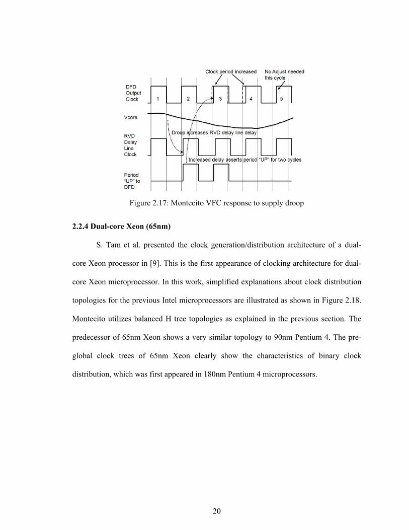
20
Figure 2.17: Montecito VFC response to supply droop
2.2.4 Dual-core Xeon (65nm)
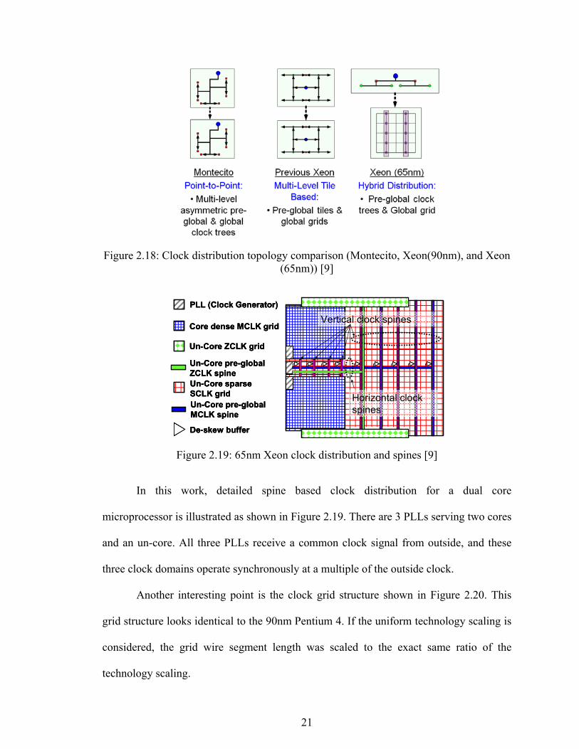
S. Tam et al. presented the clock generation/distribution architecture of a dual-
core Xeon processor in [9]. This is the first appearance of clocking architecture for dual-
core Xeon microprocessor. In this work, simplified explanations about clock distribution
topologies for the previous Intel microprocessors are illustrated as shown in Figure 2.18.
Montecito utilizes balanced H tree topologies as explained in the previous section. The
predecessor of 65nm Xeon shows a very similar topology to 90nm Pentium 4. The pre-
global clock trees of 65nm Xeon clearly show the characteristics of binary clock
distribution, which was first appeared in 180nm Pentium 4 microprocessors.
21
Figure 2.18: Clock distribution topology comparison (Montecito, Xeon(90nm), and Xeon (65nm)) [9]
Figure 2.19: 65nm Xeon clock distribution and spines [9]
In this work, detailed spine based clock distribution for a dual core
microprocessor is illustrated as shown in Figure 2.19. There are 3 PLLs serving two cores
and an un-core. All three PLLs receive a common clock signal from outside, and these
three clock domains operate synchronously at a multiple of the outside clock.
Another interesting point is the clock grid structure shown in Figure 2.20. This
grid structure looks identical to the 90nm Pentium 4. If the uniform technology scaling is
considered, the grid wire segment length was scaled to the exact same ratio of the
technology scaling.
PLL (Clock Generator)
Core dense MCLK grid
Un-Core pre-global MCLK spine
Un-Core sparse SCLK grid
De-skew buffer
Un-Core ZCLK grid
Un-Core pre-global ZCLK spine
Horizontal clock spines
Vertical clock spines
PLL (Clock Generator)PLL (Clock Generator)
Core dense MCLK gridCore dense MCLK grid
Un-Core pre-global MCLK spineUn-Core pre-global MCLK spine
Un-Core sparse SCLK gridUn-Core sparse SCLK grid
De-skew bufferDe-skew buffer
Un-Core ZCLK gridUn-Core ZCLK grid
Un-Core pre-global ZCLK spineUn-Core pre-global ZCLK spine
Horizontal clock spines
Vertical clock spines
22
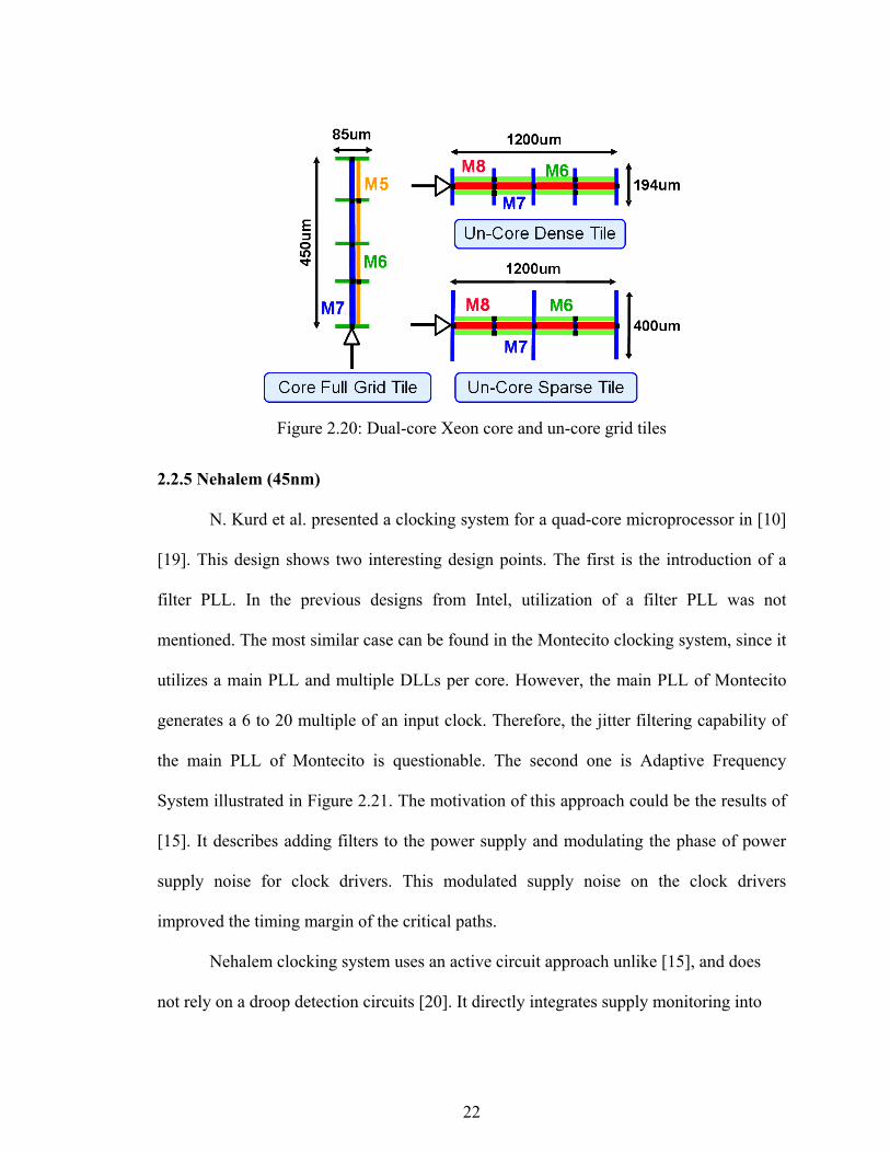
Figure 2.20: Dual-core Xeon core and un-core grid tiles
2.2.5 Nehalem (45nm)
N. Kurd et al. presented a clocking system for a quad-core microprocessor in [10]
[19]. This design shows two interesting design points. The first is the introduction of a
filter PLL. In the previous designs from Intel, utilization of a filter PLL was not
mentioned. The most similar case can be found in the Montecito clocking system, since it
utilizes a main PLL and multiple DLLs per core. However, the main PLL of Montecito
generates a 6 to 20 multiple of an input clock. Therefore, the jitter filtering capability of
the main PLL of Montecito is questionable. The second one is Adaptive Frequency
System illustrated in Figure 2.21. The motivation of this approach could be the results of
[15]. It describes adding filters to the power supply and modulating the phase of power
supply noise for clock drivers. This modulated supply noise on the clock drivers
improved the timing margin of the critical paths.
Nehalem clocking system uses an active circuit approach unlike [15], and does
not rely on a droop detection circuits [20]. It directly integrates supply monitoring into
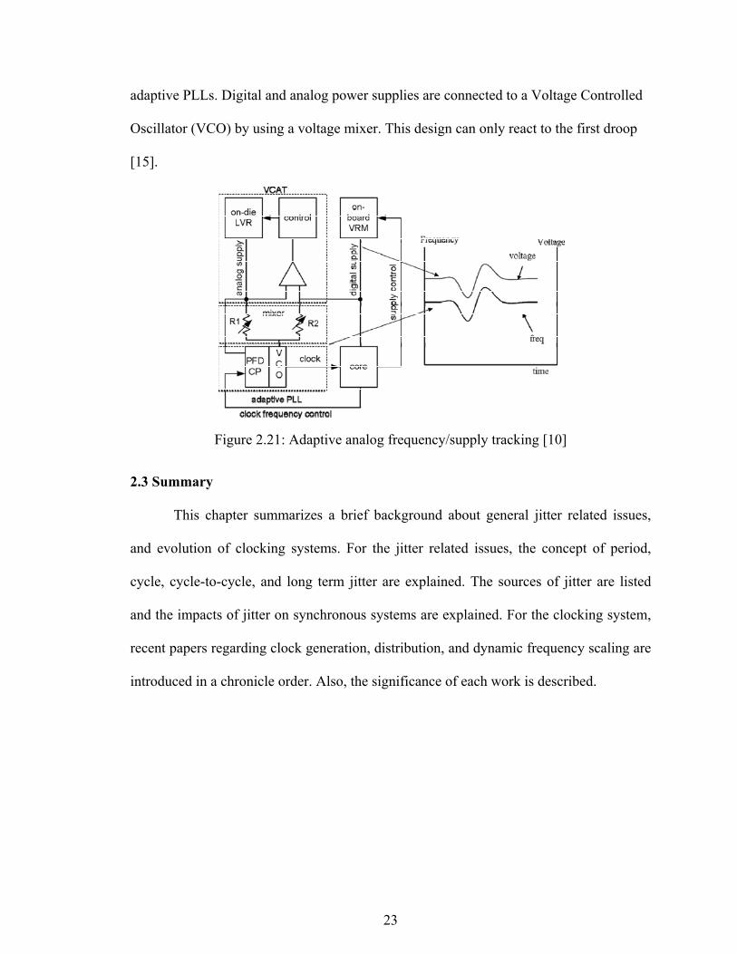
23
adaptive PLLs. Digital and analog power supplies are connected to a Voltage Controlled
Oscillator (VCO) by using a voltage mixer. This design can only react to the first droop
[15].
Figure 2.21: Adaptive analog frequency/supply tracking [10]
2.3 Summary
This chapter summarizes a brief background about general jitter related issues,
and evolution of clocking systems. For the jitter related issues, the concept of period,
cycle, cycle-to-cycle, and long term jitter are explained. The sources of jitter are listed
and the impacts of jitter on synchronous systems are explained. For the clocking system,
recent papers regarding clock generation, distribution, and dynamic frequency scaling are
introduced in a chronicle order. Also, the significance of each work is described.
24
CHAPTER 3
CLOCK DISTRIBUTION MODELING
Many different types of jitter (period jitter, cycle-to- cycle jitter, and long term
jitter) due to time varying supply noise have been some of the most important issues in
the performance of high-end microprocessors. Period jitter, in particular, is the most
disconcerting type of jitter for synchronous design styles, because it represents elongated
and shrunken clock periods in the time domain. The shortest clock period among all time
varying clock periods, the worst case period jitter (WPJ), has been chosen as the
maximum clock period of a particular design to avoid timing failures in traditional worst
case based designs.
Rahal-Arabi [21] showed that removing a large amount of on-die decoupling
capacitors could increase the maximum clock frequency. This result implies that if the
clock period variation (period jitter) tracks delay variation of the critical paths in the
presence of time varying supply noise, the maximum clock frequency can be pushed
higher than ever before. This phenomenon is generally refer to as Clock Data
Compensation (CDC) [15], and a very good graphical explanation of CDC can be found
in [22], [23].
This discovery fueled various studies regarding the relationship between power
supply noise and clock jitter in the clock distribution networks to achieve better
performance. Saint-Laurent and Swaminatha [24] presented an approximated model of
delay variation in interconnect dominated paths. Jang et al. [25] formulated cycle-to-
cycle jitter for a point-to-point clock distribution. Wong et al. [15] formulated a period
jitter expression based on a homogeneous delay line assumption. Kantorovich and
25
Houghton [26] presented an approximated period jitter expression based on propagation
delay sensitivity tests. Our own work (Jang et al. [1] [2]) presented period jitter
expressions for binary clock distributions. L. Chen et al. [27] presented period jitter
expressions for clock buffer chains.
Period jitter is a function of many different parameters such as supply noise
amplitude, supply noise frequency, clock driver size, physical structures of interconnects,
number of clock stages, temperature, process corners, etc. Due to this complicated
relationshp, all the previous works were based on very simplified clock tree assumptions;
consequently, achieving HSPICE level accuracy was almost impossible. This chapter
describes a clock distribution and power supply model used throughout this work.
3.1 Clock Distribution Modeling
Section 3.1.1 and 3.1.2 describe basic assumptions about the binary clock tree,
power supply noise and timing notations. These basic assumptions will be used to model
analytical period jitter expressions in the following sections. In Section 3.1.1, the
assumptions about 32nm technology parameters are also explained, and those are used to
compare the results from HSPICE simulations and the analytical expressions throughout
this work.
3.1.1 Global Binary Clock Tree Topology
Binary clock trees are a type of balanced clock distribution. Characteristics of
binary clock tree are well explained in [28].
26
“A binary tree on the other hand is intended to deliver the clock in a balanced
manner in either the vertical or horizontal dimension. All branches of a binary tree
exhibit identical buffer-interconnect segments, zero structural skew, and similar PVT
tracking. In contrast to the H-tree, the buffers in a binary tree can be designed to co-locate
in close proximity along a centralized stripe. The closer physical proximity of the buffers
in a binary tree can result in reduced sensitivity to on-die variation. Moreover, physical
placement of the clock buffers in close proximity will minimize floor-plan disruptions.” –
S. Tom [28].
The terminology “binary tree” is not related to the same terminology used in
clock tree synthesis community [29].
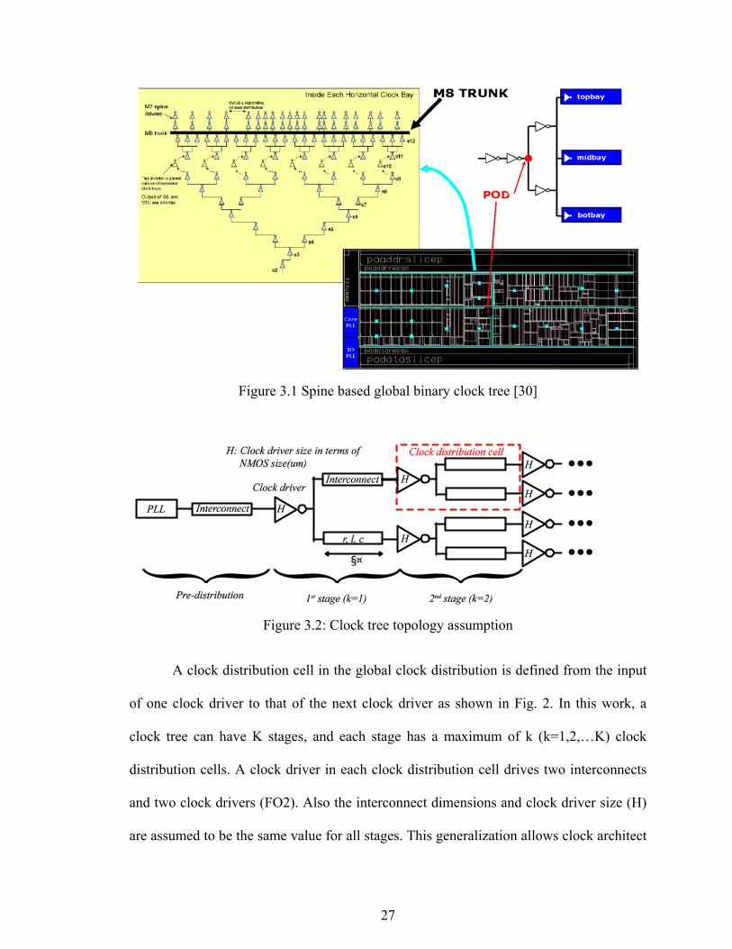
Figure. 3.2 illustrates a global binary clock tree, and this is a generalized topology
of Figure.3.1. A clock signal generated by a PLL tends to be distributed to the center of
the microprocessor by using a pre-distribution network. After that, the clock signal is
distributed through a global binary clock tree.
27
Figure 3.1 Spine based global binary clock tree [30]
Figure 3.2: Clock tree topology assumption
A clock distribution cell in the global clock distribution is defined from the input
of one clock driver to that of the next clock driver as shown in Fig. 2. In this work, a
clock tree can have K stages, and each stage has a maximum of k (k=1,2,…K) clock
distribution cells. A clock driver in each clock distribution cell drives two interconnects
and two clock drivers (FO2). Also the interconnect dimensions and clock driver size (H)
are assumed to be the same value for all stages. This generalization allows clock architect
28
to work in higher level to evaluate possible choices based on available information at the
planning stage of clock distribution without violating the clock distribution methodology
shown in Figure 3.1.
In the binary tree based clock distribution, the same length of clock distribution
can be designed with different numbers of clock stages, which utilize different
interconnect lengths. For example, a 10mm long clock tree can consist of either 10 stages
with 1000um interconnects per stage, 20 stages with 500um interconnects per stage, or 40
stages with 250um interconnects per stage. There can be many different combinations to
choose, but these three combinations are chosen to see the impacts of different wire
lengths and clock stage counts on period jitter.
32nm BSIM4 MOSFET models from Predictive Technology Model (PTM) [31]
and global interconnect dimensions based on Intel 32nm Technology [32] are used to
model a 32nm technology node. HSPICE simulations are used to decide the proper clock
driver size and interconnect width that generate the realistic rise and fall time (10% of
TCLK=3GHz) for each option. The smallest clock driver and interconnect width that
satisfy the rise and fall time requirements are chosen and tabulated in TABLE 3.1, and
the crosscut view of the global interconnect model is shown in Figure.3.3. The
interconnects are modeled as RLC interconnects. The reason is to enable seamless
analyses for small and large clock driver sizes at the same time; when the rise/fall
transitions of an input signal into a long global interconnect are very fast due to a large
clock driver size, the effect of the inductance can be more pronounced. Also, as the clock
driver size is reduced, the inductive effect will be less pronounced, and the interconnect
will act like a simple RC interconnect. For RLC value extraction, FastHenry and FastCap
29
are used. It is also confirmed that the extracted RL parameters are valid across a wide
range of AC frequencies. HSPICE W-elements are used to model interconnects for circuit
simulations.
Table 3.1: Clock driver sizes and interconnect parameters
\ Option 1 Option 2 Option 3 Clock Stage 10 20 40 Clock Driver Size 15um 12um 6um Interconnect length, (ℓ) 1000um 500um 250um Interconnect width, (W) 225nm x 3 225nm 225nm Interconnect space, (S) 450nm Interconnect Height, (H) 388nm ILD thickness (t) 252nm Dielectric(εr) 1.8 Processor corner TT Temperature 80˚ Fclk 3GHz VDD 1.1V
Figure 3.3: Crosscut view of global interconnect structures
3.1.2 Power Supply Noise and Timing Notation
Pant and Chiprout [33] show that high and mid frequency (fn>1GHz) power
supply noises that could appear as a result of high activity function blocks are highly
30
localized. Also spine based global binary trees are placed outside of large function blocks
as shown in Figure. 3.1. On the top of these, a simple low-pass RC filter can be utilized to
reduce the high and mid frequency power supply noise [10] [34].
These three facts imply that the clock drivers in the global clock distribution will
see low frequency noise (100-400MHz), and a supply noise in this frequency range is
stated as the first droop in [15]. Also, the low frequency noise is likely to be shared by the
entire power supply distribution network, and it tends to resonate over a very long time.
Based on these facts, it is assumed that the power supply pins of all clock drivers are
experiencing a common global supply noise, and it is formulated as a sinusoidal
waveform.
( ) ( )2 sin 2 ,n n nv t V f tπ φ= +
(3.1)
where 2Vn is the amplitude of power supply noise. It is also assumed that the supply
noise frequency (fn) is very low compared to the clock frequency of a high-end
microprocessor (fn<<fCLK). The supply noise is not modeled as a damped sinusoidal noise
in this paper due to two reasons: 1) for the sake of mathematical simplicity, and 2) the
worst case period jitter (WPJ) happens when the supply noise transits from the lowest
voltage to highest voltage. The WPJ due to a damped sinusoidal supply noise is almost
identical to the WPJ due to a sinusoidal supply noise.
31
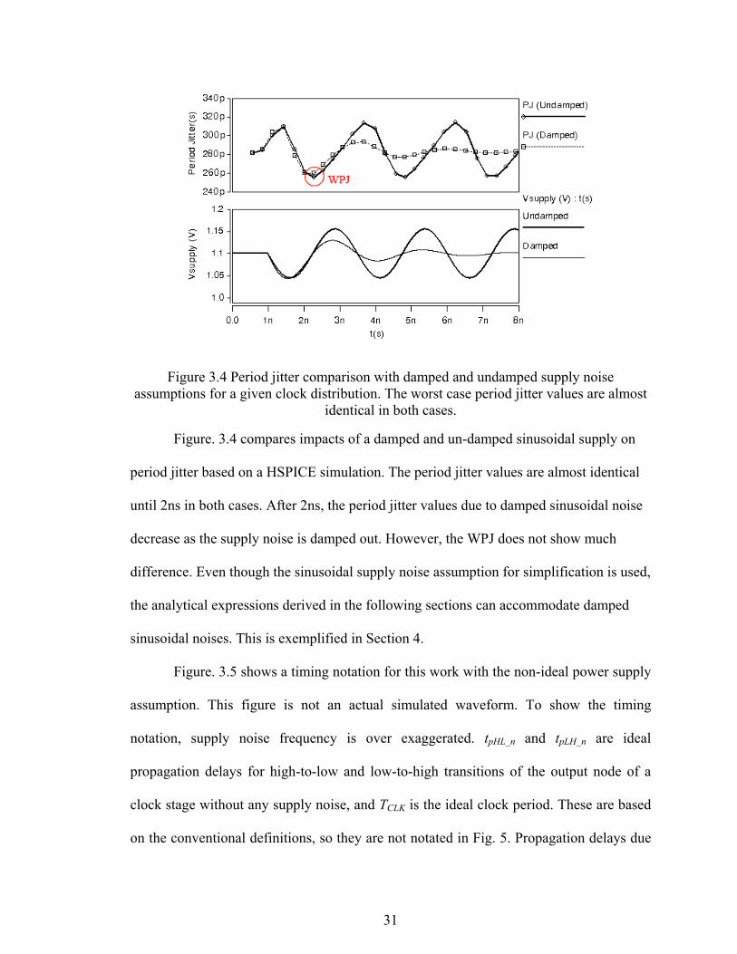
Figure 3.4 Period jitter comparison with damped and undamped supply noise assumptions for a given clock distribution. The worst case period jitter values are almost
identical in both cases.
Figure. 3.4 compares impacts of a damped and un-damped sinusoidal supply on
period jitter based on a HSPICE simulation. The period jitter values are almost identical
until 2ns in both cases. After 2ns, the period jitter values due to damped sinusoidal noise
decrease as the supply noise is damped out. However, the WPJ does not show much
difference. Even though the sinusoidal supply noise assumption for simplification is used,
the analytical expressions derived in the following sections can accommodate damped
sinusoidal noises. This is exemplified in Section 4.
Figure. 3.5 shows a timing notation for this work with the non-ideal power supply
assumption. This figure is not an actual simulated waveform. To show the timing
notation, supply noise frequency is over exaggerated. tpHL_n and tpLH_n are ideal
propagation delays for high-to-low and low-to-high transitions of the output node of a
clock stage without any supply noise, and TCLK is the ideal clock period. These are based
on the conventional definitions, so they are not notated in Fig. 5. Propagation delays due
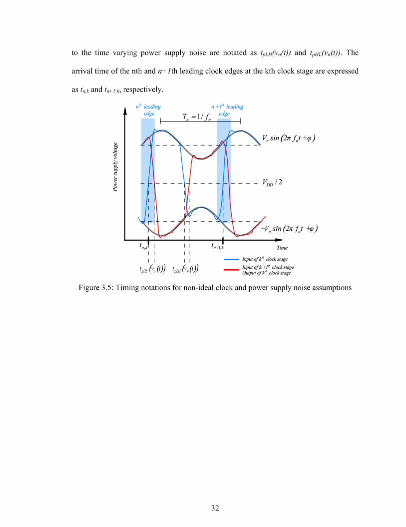
32
to the time varying power supply noise are notated as tpLH(vn(t)) and tpHL(vn(t)). The
arrival time of the nth and n+1th leading clock edges at the kth clock stage are expressed
as tn,k and tn+1,k, respectively.
Figure 3.5: Timing notations for non-ideal clock and power supply noise assumptions
33
CHAPTER 4
SUPPLY NOISE INDUCED PERIOD JITTER
IN GLOBAL CLOCK DISTRIBUTION
4.1 Recursive Period Jitter Expression
Period jitter, from its definition [12], is formulated as follows:
( ) ( ), ,1, ,
( , )
n k n kCLK n k n k
n kCLK
PJ T t t
CJ T
+= = −
= +
(4.1)
The nth period jitter at the kth stage (PJ(n,k)) is just the nth clock period at kth stage.
The period jitter is modeled as propagation delay variations of two leading edges [25]
[35]. Also, cycle jitter (CJ(n,k)) is the nth clock period (TCLK(n,k)) minus the nominal clock
period (TCLK). This implies period jitter and cycle jitter are interchangeable with TCLK
offset. Cycle-to-cycle jitter and long term jitter can also be expressed in the similar
expressions based on [35].
4. 2 Propagation Delay Sensitivity of Clock Distribution Cells due to Static Supply Noise
Propagation delay of a clock distribution cell can vary over different static power
supply voltages. This variation is referred to as propagation delay sensitivity in this work.
An example of the power supply sensitivity test is shown in Figure. 4.1.
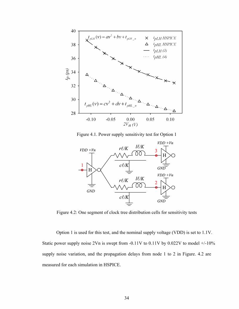
34
Figure 4.1. Power supply sensitivity test for Option 1
Figure 4.2: One segment of clock tree distribution cells for sensitivity tests
Option 1 is used for this test, and the nominal supply voltage (VDD) is set to 1.1V.
Static power supply noise 2Vn is swept from -0.11V to 0.11V by 0.022V to model +/-10%
supply noise variation, and the propagation delays from node 1 to 2 in Figure. 4.2 are
measured for each simulation in HSPICE.
35
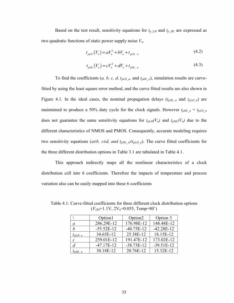
Based on the test result, sensitivity equations for tp_LH and tp_HL are expressed as
two quadratic functions of static power supply noise Vn.
( ) 2_pLH n n n pLH nt V aV bV t= + +
(4.2)
( ) 2_pHL n n n pHL nt V cV dV t= + +
(4.3)
To find the coefficients (a, b, c, d, tpLH_n, and tpHL_n), simulation results are curve-
fitted by using the least square error method, and the curve fitted results are also shown in
Figure 4.1. In the ideal cases, the nominal propagation delays (tpHL_n and tpLH_n) are
maintained to produce a 50% duty cycle for the clock signals. However tpHL_n = tpLH_n
does not guarantee the same sensitivity equations for tpLH(Vn) and tpHL(Vn) due to the
different characteristics of NMOS and PMOS. Consequently, accurate modeling requires
two sensitivity equations (a≠b, c≠d, and tpHL_n≠tpLH_n). The curve fitted coefficients for
the three different distribution options in Table 3.1 are tabulated in Table 4.1.
This approach indirectly maps all the nonlinear characteristics of a clock
distribution cell into 6 coefficients. Therefore the impacts of temperature and process
variation also can be easily mapped into these 6 coefficients
Table 4.1: Curve-fitted coefficients for three different clock distribution options (VDD=1.1V, 2Vn=0.055, Temp=80˚)
\ Option1 Option2 Option 3 a 286.29E-12 176.98E-12 148.48E-12 b -55.52E-12 -40.75E-12 -42.28E-12 tpLH n 34.65E-12 25.38E-12 18.15E-12 c 259.01E-12 191.47E-12 173.02E-12 d -47.17E-12 -38.73E-12 -39.51E-12 tpHL n 30.18E-12 20.76E-12 15.32E-12
36
4.3 Recursive Period Jitter Expression
For a K stage clock distribution, the nth leading clock edge arrives at the first
clock driver at time tn,1. The arrival time of the nth leading clock edge at the output node
of Kth stage is formulated as (4.4). Also, the arrival time of n+1th edge at the output node
of Kth stage is formulated as (4.5). For simplicity, only the even numbered clock stages
were assumed. However, the odd numbered clock distribution can be formulated with the
exact same approach.
The recursive period jitter equation, (4.6), is the result of the following
phenomenon. When the nth leading clock edge is sent at time tn,1, the presence of a
shared global power supply noise varies the supply voltage of all clock drivers. The
supply noise modulates the propagation delay of the first clock stage. Again, this
modulated propagation delay plus tn,1 forms tn,2 , and this decides the next power supply
noise value which the clock driver of the second stage will experience. Again, the same
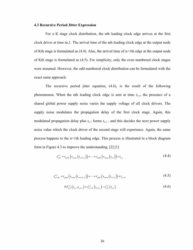
process happens to the n+1th leading edge. This process is illustrated in a block diagram
form in Figure 4.3 to improve the understanding. [2] [1]
( )( ) ( )( )( ), , 1 ,1 ,1r
n K pLH noise n K pHL noise n nt t v t t v t t−= + + + (4.4)
( )( ) ( )( )( )1, 1, 1 1,1 1,1
rn K pLH noise n K pHL noise n nt t v t t v t t+ + − + += + + + (4.5)
( ) ( ) ( )( ) ( ) ( ), ,1 1,1 1, 1,1 , ,1, .r r r
n K n n n K n n K nPJ t t t t t t+ + += − (4.6)
37
Figure 4.3. Block diagram representation of the recursive period jitter
Another notable point is that the recursive period jitter expression, PJ(r)n,K, can
handle the input jitter of clock trees from other sources. Examples of these sources could
be a PLL or a pre-distribution network as shown in Figure. 3.2. The modeling of input
jitter is enabled by tn,1 and tn+1,1 terms in (4.4) and (4.5), which do form input period jitter
(PJ(r)n,1=tn+1,1-tn,1).
4.3.1 Comparison between HSPICE Simulation and Analytical Expression
4.3.1.1 Considerations for Circuit Simulations
First, we have to consider whether the circuit simulations will generate
meaningful results. Let’s assume a PLL will generate a clean clock signal. However, the
phase relationship between the clock signal and the supply noise is hard to pinpoint at the
beginning of microprocessor design stage, even though they are correlated. The exact
relationship depends upon the final implementation of a microprocessor (e.g. clock gating
and power up procedure). This mandates studies of period jitter with different phase
relationships between the leading edge of the clock signal and the phase of power supply.
38
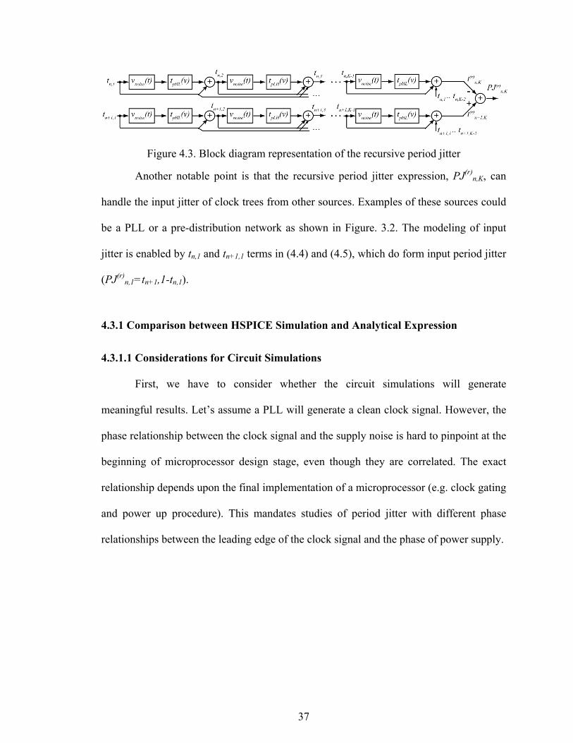
Figure 4.4. An example of ineffective simulation
Let’s assume fCLK is an integer multiple of fn. (e.g. fCLK=3.2GHz, and
fn=400MHz). This simulation condition most likely will generate not so useful results
regardless of total simulation duration. Let’s assume the nth leading edges see vnoise(t0).
The n+8th leading edge will see the exact same supply noise. This also applies to the
n+1th and n+9th leading edges as shown in Figure. 4.4. This continues regardless of total
simulation duration. Even if the fCLK is not an integer multiple of fn, this requires very
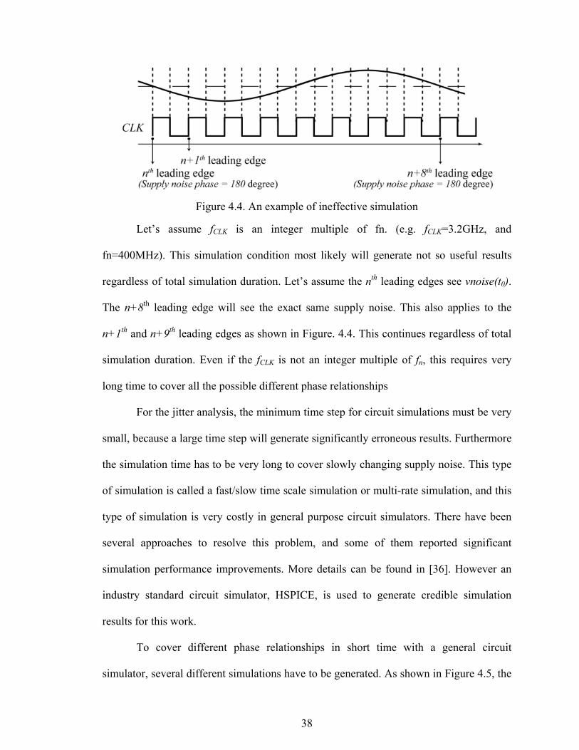
long time to cover all the possible different phase relationships
For the jitter analysis, the minimum time step for circuit simulations must be very
small, because a large time step will generate significantly erroneous results. Furthermore
the simulation time has to be very long to cover slowly changing supply noise. This type
of simulation is called a fast/slow time scale simulation or multi-rate simulation, and this
type of simulation is very costly in general purpose circuit simulators. There have been
several approaches to resolve this problem, and some of them reported significant
simulation performance improvements. More details can be found in [36]. However an
industry standard circuit simulator, HSPICE, is used to generate credible simulation
results for this work.
To cover different phase relationships in short time with a general circuit
simulator, several different simulations have to be generated. As shown in Figure 4.5, the
39
different phase relationships between the leading edges and supply noise have to be
generated and separately simulated. In this work, most simulation results were generated
based on 60 different simulations (phase relationship granularity of 2π/60).
Figure 4.5. Simulation methodology to cover different phase relationships
4.3.1.2 Comparisons between HSPICE and Recursive Expression
Figure 4.6 compares the results between HSPICE simulations and the recursive
analytical expression, (4.6). The x-axis and y-axis represent the tn,1 in terms of power
supply noise phase and period jitter, respectively. This plotting style is derived from two
facts. First, period jitter is defined by two leading edges as formulated in (4.6). Among
the two leading edge positions at the first clock driver (tn,1 and tn+1,1), the tn,1 is selected
as a reference point. Second, a globally shared power supply noise is modeled as a
periodic sinusoidal waveform. This implies that the tn,1 compared to the supply noise
phase uniquely decides the power supply noise experienced by the clock drivers.
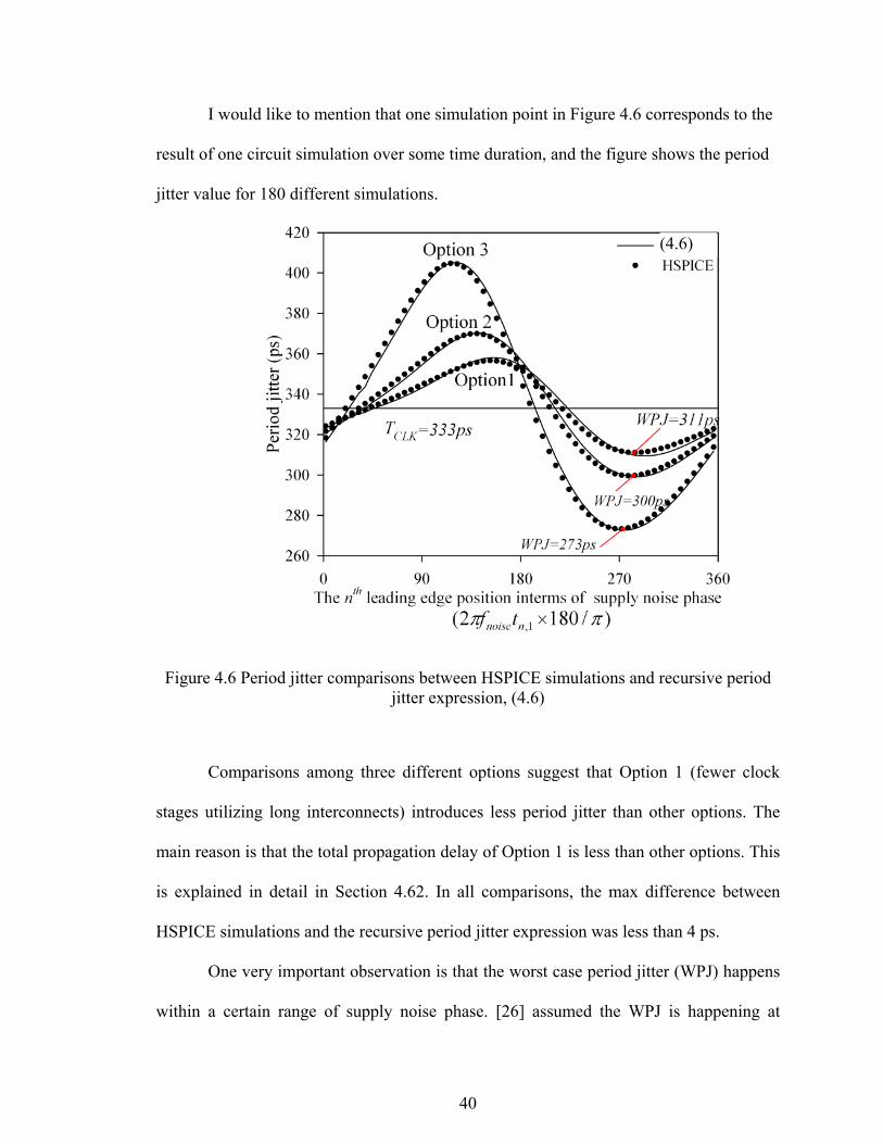
40
I would like to mention that one simulation point in Figure 4.6 corresponds to the
result of one circuit simulation over some time duration, and the figure shows the period
jitter value for 180 different simulations.
Figure 4.6 Period jitter comparisons between HSPICE simulations and recursive period jitter expression, (4.6)
Comparisons among three different options suggest that Option 1 (fewer clock
stages utilizing long interconnects) introduces less period jitter than other options. The
main reason is that the total propagation delay of Option 1 is less than other options. This
is explained in detail in Section 4.62. In all comparisons, the max difference between
HSPICE simulations and the recursive period jitter expression was less than 4 ps.
One very important observation is that the worst case period jitter (WPJ) happens
within a certain range of supply noise phase. [26] assumed the WPJ is happening at
(4.6)
41
specific supply point. While this might be true for certain clock distributions topologies,
assuming that the WPJ happens at a specific point might lead to inaccurate WPJ
estimation. Therefore, the WPJ has to be searched in a range of possible first leading
edge positions to find out the real WPJ.
Even though the recursive expression predicts period jitter with great accuracy, it
has two major drawbacks; 1) its complexity limits physical insight into the relationship
between clock design parameters and period jitter, and 2) the worst case period jitter
position in the time domain cannot be formulated based on the recursive expression.
These two issues are addressed in the following sections.
4.4 Non-recursive Period Jitter Expression
Even though jitter predictions based on the recursive expression (4.6) are very
accurate, they can give little physical insight due to their recursive nature. To shed light
on the physical process of period jitter in the time domain, (4.4) and (4.5) are converted
to non-recursive expressions by breaking their recursive relationship. For this section,
only the even numbered clock distribution stages were assumed for the sake of simplicity.
If the nth leading edge arrives at the 1st stage at tn,1, the clock driver at the 1st stage
will see the supply noise of vnoise(tn,1). If the total propagation delay through K clock
stages is significantly smaller than the supply noise period (tn,K-tn,1<<Tn), the supply
noise experienced by each clock driver with and without delay modulation will be almost
same:
, ≈ , + ( _ + _ )/2 (4.7)
When (4.7) is satisfied, the recursive expressions (4.4, 4.5, and 4.6) can be
approximated to non-recursive expressions (9,10, and 11), respectively..
42
( )( )( ) ( )( )( )( )
( ) ( )( ) ( )( )( )( )( 2) / 2 ,1 ,1 ,1
( ), ,1 ,1
0,1 ,1 ,11
K pHL noise pHL noise n pLH noise n nnr
n K n ni
pLH noise pHL noise n pLH noise n n
t v i t v t i t v t tt t t
t v i t v t i t v t t
−
=
× + × + + = + + × + × +
(4.8)
( )( )( ) ( )( )( )( )
( ) ( )( ) ( )( )( )( )( 2) / 2 ,1 ,1 1,1
( )1, 1,1 1,1
0,1 ,1 1,11
K pHL noise pHL noise n pLH noise n nnr
n K n ni
pLH noise pHL noise n pLH noise n n
t v i t v t i t v t tt t t
t v i t v t i t v t t
− +
+ + +=
+
× + × + + = + + × + × +
(4.9)
( ) ( ) ( )( ) ( ) ( ), ,1 1,1 1, 1,1 , ,1, .nr nr nr
n K n n n K n n K nPJ t t t t t t+ + += − (4.10)
Unfortunately, the recursive nature and complexity of tn,K disable the formulation
of more detailed approximation conditions. However, the accuracy of approximation can
be easily tested by comparing t(r)n,K and t(nr)
n,K, (4.8 and 4.9). The test can be summarized
as follows:
( ) ( ), , .nr r
n K n Kt t tolerance− ≤
Figure 4.7 represents the approximation accuracies for three different clock stage
settings based on Option 2 in Table 3.1 with 1ps tolerances. The left side of each line in
the plot represents that the error between recursive and non-recursive expressions (4.4
and 4.8) is less than the given tolerance for the given power supply noise frequency and
amplitude combinations. The shaded region (100≤fn≤400MHz, 2Vn≤0.11) represents the
power supply noise of the first droop in [15]. The power supply noise of this shaded
region can severely impact performance of a microprocessor by reducing clock period,
but it can only be mitigated through on-die decoupling capacitors. This cannot be
mitigated after the tape-out unlike the outside of the shaded region [15]. As a result, this
region of supply noise condition is the main concern among other supply noise conditions.
Figure 4.7 suggests that this approximated equation effectively covers the most
disconcerting supply noise combinations. When K is equal to 26, some supply noise
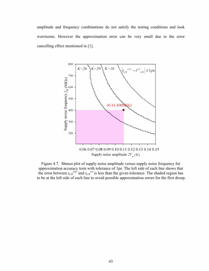
43
amplitude and frequency combinations do not satisfy the testing conditions and look
worrisome. However the approximation error can be very small due to the error
cancelling effect mentioned in [1].
Figure 4.7. Shmoo plot of supply noise amplitude versus supply noise frequency for approximation accuracy tests with tolerance of 1ps. The left side of each line shows that the error between tn,K
(nr) and tn,K(r) is less than the given tolerance. The shaded region has
to be at the left side of each line to avoid possible approximation errors for the first droop.
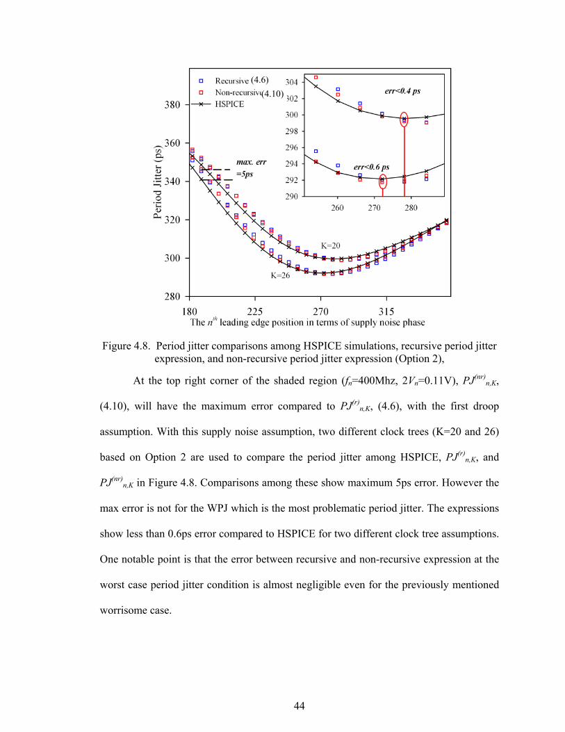
44
Figure 4.8. Period jitter comparisons among HSPICE simulations, recursive period jitter expression, and non-recursive period jitter expression (Option 2),
At the top right corner of the shaded region (fn=400Mhz, 2Vn=0.11V), PJ(nr)n,K,
(4.10), will have the maximum error compared to PJ(r)n,K, (4.6), with the first droop
assumption. With this supply noise assumption, two different clock trees (K=20 and 26)
based on Option 2 are used to compare the period jitter among HSPICE, PJ(r)n,K, and
PJ(nr)n,K in Figure 4.8. Comparisons among these show maximum 5ps error. However the
max error is not for the WPJ which is the most problematic period jitter. The expressions
show less than 0.6ps error compared to HSPICE for two different clock tree assumptions.
One notable point is that the error between recursive and non-recursive expression at the
worst case period jitter condition is almost negligible even for the previously mentioned
worrisome case.
(4.6)
(4.10)
45
What is the physical implication regarding the fact that the recursive expression
can be approximated into a non-recursive expression for the first droop supply noise
conditions? It implies the recursive characteristic is not a dominant contributor for the
first droop. The total propagation delay through a clock distribution (tn,K and tn+1,K) can
change significantly, in percentage, compared to the total nominal propagation delay
without supply noise. For example, the total nominal propagation delay for Option 2 is
around 450ps, but the worst case propagation delay will be around 510ps (13% more
delay). However, the clock drivers see almost identical supply noise voltage values
compared to the supply noise seen by clock drivers without delay variation. For example,
the last stage clock driver (K=20) will see 2Vnsin(2π fn 510ps), but this is almost identical
to 2Vn sin(2 π fn 450ps) for the first droop supply noise condition. This concludes the
recursive characteristic is not a dominant factor which decides period jitter with the first
droop assumption. The dominant factor is pointed out in section 4.6.2.
4.5 Worst Case Period Jitter
The most critical part of period jitter is the worst case period jitter (WPJ), because
it represents the shortest clock period. The position of the WPJ in the time domain is a
complex function of several different design parameters.
Numerically finding the WPJ is very trivial. Based on numerical search of the
recursive/non-recursive expressions, the WPJ can be found in a second. However
analytically solving when the WPJ appears in time domain can give some insight into the
period jitter reduction for the binary clock distribution. Also, finding the exact time point
when the WPJ happens is very important to reduce unnecessary circuit simulations,
because finding out the WPJ requires at least 6~10 iterations. (The exact iterations defend
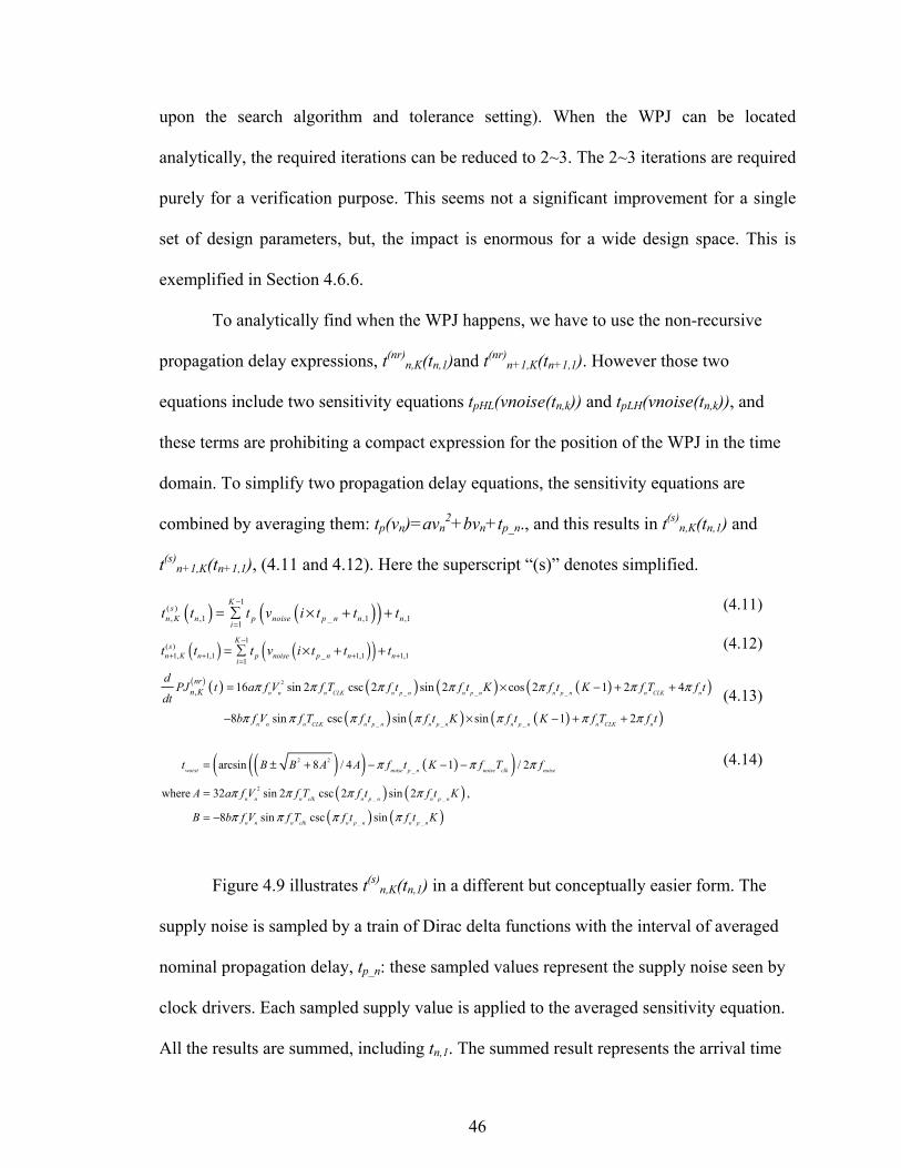
46
upon the search algorithm and tolerance setting). When the WPJ can be located
analytically, the required iterations can be reduced to 2~3. The 2~3 iterations are required
purely for a verification purpose. This seems not a significant improvement for a single
set of design parameters, but, the impact is enormous for a wide design space. This is
exemplified in Section 4.6.6.
To analytically find when the WPJ happens, we have to use the non-recursive
propagation delay expressions, t(nr)n,K(tn,1)and t(nr)
n+1,K(tn+1,1). However those two
equations include two sensitivity equations tpHL(vnoise(tn,k)) and tpLH(vnoise(tn,k)), and
these terms are prohibiting a compact expression for the position of the WPJ in the time
domain. To simplify two propagation delay equations, the sensitivity equations are
combined by averaging them: tp(vn)=avn2+bvn+tp_n., and this results in t(s)
n,K(tn,1) and
t(s)n+1,K(tn+1,1), (4.11 and 4.12). Here the superscript “(s)” denotes simplified.
( ) ( )( )1( ), ,1 _ ,1 ,1
1
Ks
n K n p noise p n n ni
t t t v i t t t−
== × + + (4.11)
( ) ( )( )1( )
1, 1,1 _ 1,1 1,11
Ks
n K n p noise p n n ni
t t t v i t t t−
+ + + +=
= × + + (4.12)
( ) ( ) ( ) ( ) ( )( )
( ) ( ) ( )( )
2
_ _ _
_ _ _
, 16 sin 2 csc 2 sin 2 cos 2 1 2 4
8 sin csc sin sin 1 2
n n n CLK n p n n p n n p n n CLK n
n n n CLK n p n n p n n p n n CLK n
nrn K
dPJ t a f V f T f t f t K f t K f T f t
dt
b f V f T f t f t K f t K f T f t
π π π π π π π
π π π π π π π
= × − + +
− × − + +
(4.13)
( )( ) ( )( )( ) ( )
( ) ( )
2 2
_
2
_ _
_ _
arcsin 8 / 4 1 / 2
where 32 sin 2 csc 2 sin 2 ,
8 sin csc sin
worst noise p n noise clk noise
n n n clk n p n n p n
n n n clk n p n n p n
t B B A A f t K f T f
A a f V f T f t f t K
B b f V f T f t f t K
π π π
π π π π
π π π π
= ± + − − −
=
= −
(4.14)
Figure 4.9 illustrates t(s)n,K(tn,1) in a different but conceptually easier form. The
supply noise is sampled by a train of Dirac delta functions with the interval of averaged
nominal propagation delay, tp_n: these sampled values represent the supply noise seen by
clock drivers. Each sampled supply value is applied to the averaged sensitivity equation.
All the results are summed, including tn,1. The summed result represents the arrival time
47
of nth leading edge at the Kth stage, t(s)n,K(tn,1). This formulation is based on the conclusion
at the end of Section 4.4. Because the recursive characteristic is not a dominant factor, we
can separate the supply noise sampling from the summation of delay variation.
Figure 4.9. Block diagram explanation of simplified non-recursive expression.
Based on these simplifications, the derivative of period jitter expression in the
time domain is found as shown in (4.13), and (4.14) is solved for time t by setting (4.13)
to 0. We also assumed tn+1,1=tn,1+TCLK. By doing this, we can simplify the equations
further, but (4.13) and (4.15) lose the ability to find the WPJ with consideration of the
input jitter of clock trees.
(4.13) and (4.14) reveal four different conditions which result in zero jitter:
1) fn=0 or Vn=0,
2) a=0 and b=0,
3) TCLK=n*Tn, n=1,2,3,…,
4) tp_n*K=nTn, n=1,2,3….
When the above four conditions are satisfied, the period jitter is always zero. The
first condition indicates there has to be no noise. The third and forth conditions are
achievable by adjusting the TCLK and tp_n*K (total nominal propagation delay) through a
global clock tree, but they are not practical: increasing the TCLK is simply not acceptable
in terms of performance, and increasing tp_n*K requires more clock stages, power, and
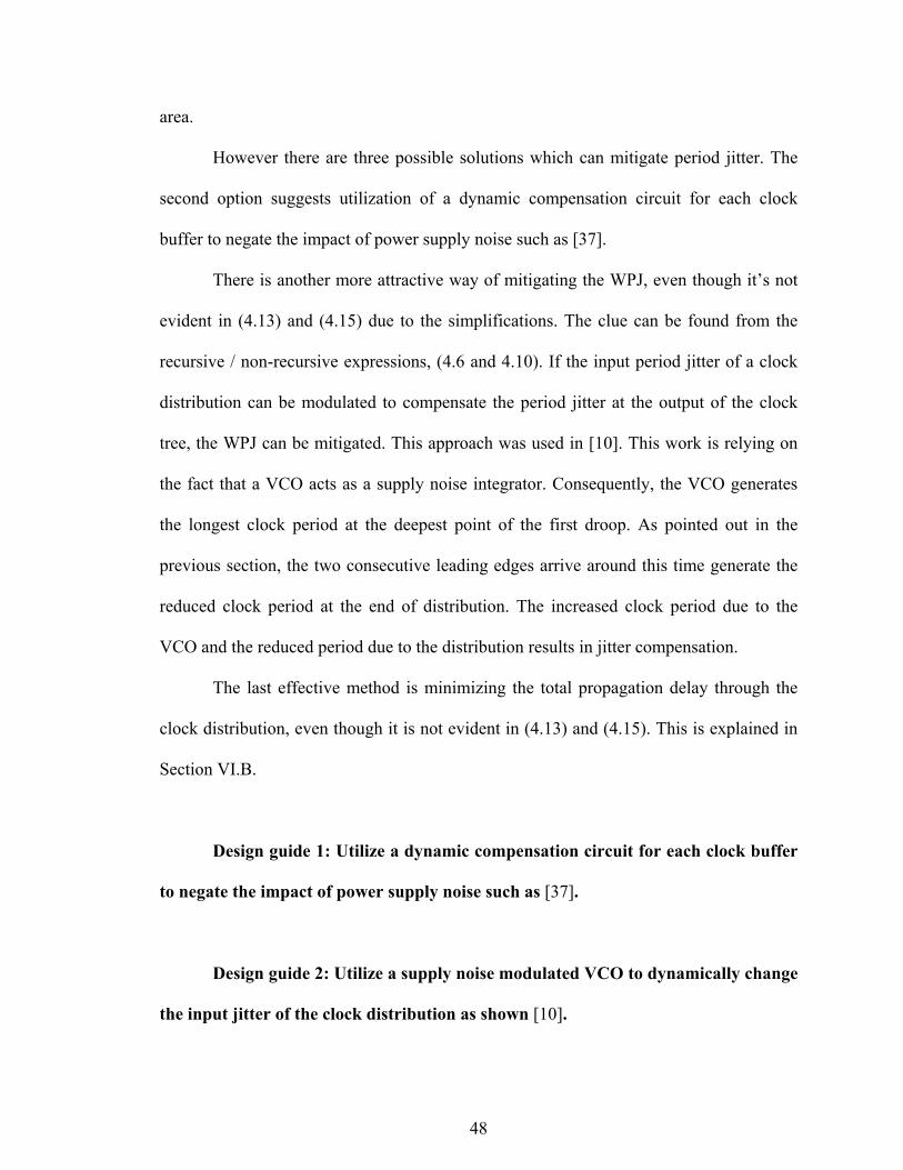
48
area.
However there are three possible solutions which can mitigate period jitter. The
second option suggests utilization of a dynamic compensation circuit for each clock
buffer to negate the impact of power supply noise such as [37].
There is another more attractive way of mitigating the WPJ, even though it’s not
evident in (4.13) and (4.15) due to the simplifications. The clue can be found from the
recursive / non-recursive expressions, (4.6 and 4.10). If the input period jitter of a clock
distribution can be modulated to compensate the period jitter at the output of the clock
tree, the WPJ can be mitigated. This approach was used in [10]. This work is relying on
the fact that a VCO acts as a supply noise integrator. Consequently, the VCO generates
the longest clock period at the deepest point of the first droop. As pointed out in the
previous section, the two consecutive leading edges arrive around this time generate the
reduced clock period at the end of distribution. The increased clock period due to the
VCO and the reduced period due to the distribution results in jitter compensation.
The last effective method is minimizing the total propagation delay through the
clock distribution, even though it is not evident in (4.13) and (4.15). This is explained in
Section VI.B.
Design guide 1: Utilize a dynamic compensation circuit for each clock buffer
to negate the impact of power supply noise such as [37].
Design guide 2: Utilize a supply noise modulated VCO to dynamically change
the input jitter of the clock distribution as shown [10].
49
If all four conditions are not satisfied, (4.13) leaves two possible solutions shown
in (4.14): the worst and best period jitter
Figure 4.10. Error (ps) between the analytically found WPJ based on (15) and PJ(r)
n,K(t)and the numerically searched WPJ based on PJ(r)n,K(t)
Figure 4.10 compares the WPJ values from numerical searches based on PJ(r)n,K(t)
with those from the predicted jitter based on the direct evaluations of PJ(r)n,K(t) at t=tworst,
which was found from (4.14) for each combination of power supply noise frequency (fn)
and supply noise amplitude (2Vn). Errors between these two approaches are plotted for
different combinations of fn and 2Vn. For these comparisons, Option 2 is used, and the
390 different combinations of fn and 2Vn from the shaded region in Figure 4.7 is used.
The plot shows the results based on both methods are nearly exact matches. The error
value increases as the signal strength of power supply noise increases. This result is
expected based on Section 4.4.
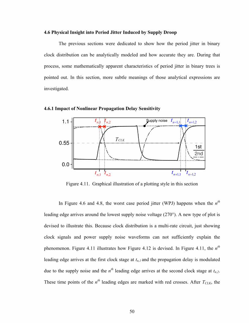
50
4.6 Physical Insight into Period Jitter Induced by Supply Droop
The previous sections were dedicated to show how the period jitter in binary
clock distribution can be analytically modeled and how accurate they are. During that
process, some mathematically apparent characteristics of period jitter in binary trees is
pointed out. In this section, more subtle meanings of those analytical expressions are
investigated.
4.6.1 Impact of Nonlinear Propagation Delay Sensitivity
Figure 4.11. Graphical illustration of a plotting style in this section
In Figure 4.6 and 4.8, the worst case period jitter (WPJ) happens when the nth
leading edge arrives around the lowest supply noise voltage (270°). A new type of plot is
devised to illustrate this. Because clock distribution is a multi-rate circuit, just showing
clock signals and power supply noise waveforms can not sufficiently explain the
phenomenon. Figure 4.11 illustrates how Figure 4.12 is devised. In Figure 4.11, the nth
leading edge arrives at the first clock stage at tn,1 and the propagation delay is modulated
due to the supply noise and the nth leading edge arrives at the second clock stage at tn,2.
These time points of the nth leading edges are marked with red crosses. After TCLK, the
51
n+1th leading edge arrives at the first clock stage at tn+1,1. The n+1th leading edges are
marked with blue crosses. The crosses are marked on the top of the supply noise to
illustrate the location of leading edges in time domain and the supply noise at the same
time. The distance between two same colored consecutive markers represents
propagation delay modulated by the supply noise.
Figure 4.12 illustrates why the WPJ happens around 270°. This is due to the
impact of nonlinear propagation delay sensitivities. Zero input jitter and one clock stage
are assumed for simplicity. The supply noise period and the propagation delay are highly
exaggerated to illustrate the phenomenon. However this type of figure appearing after in
this paper is not exaggerated. Figure 4.12 (a) shows the case when the nth leading edge
(the first red marker) arrives at the first clock driver around the lowest supply noise.
Figure 4.12 (b) shows the case when the nth leading edge arrives when the supply noise is
not around the lowest point.
In the sensitivity plot (Figure 4.1), the sensitivity change (|dtp/dVn|) at negative
voltage is higher than at positive voltage. The nth leading edge (the first red markers) at
Figure 4.12 (a) sees the lowest voltage, and this causes the largest positive delay variation.
The n+1th leading edge (the first blue marker) at (a) has small delay variation, and the
delay variation is exactly same for the nth leading at (b). The n+1th leading edge in (b)
sees the highest noise value, and this causes the largest negative delay variation. However,
the |dtp/dVn| at positive voltage is less than the |dtp/dVn| at negative voltage. In both cases,
the period jitter worsens but with different rates owing to the nonlinear sensitivity of a
clock distribution cell. This causes the WPJ happening, when the nth leading edges arrives
around the lower supply noise (270°).
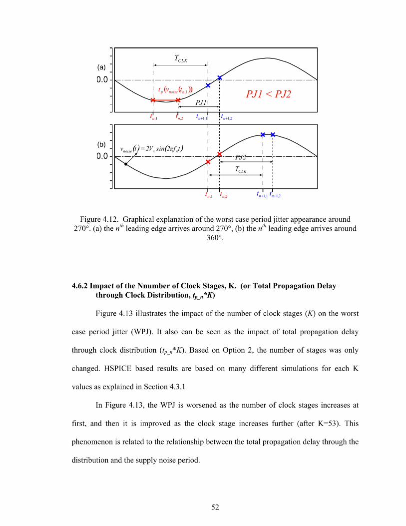
52
Figure 4.12. Graphical explanation of the worst case period jitter appearance around 270°. (a) the nth leading edge arrives around 270°, (b) the nth leading edge arrives around
360°.
4.6.2 Impact of the Nnumber of Clock Stages, K. (or Total Propagation Delay through Clock Distribution, tp_n*K)
Figure 4.13 illustrates the impact of the number of clock stages (K) on the worst
case period jitter (WPJ). It also can be seen as the impact of total propagation delay
through clock distribution (tp_n*K). Based on Option 2, the number of stages was only
changed. HSPICE based results are based on many different simulations for each K
values as explained in Section 4.3.1
In Figure 4.13, the WPJ is worsened as the number of clock stages increases at
first, and then it is improved as the clock stage increases further (after K=53). This
phenomenon is related to the relationship between the total propagation delay through the
distribution and the supply noise period.
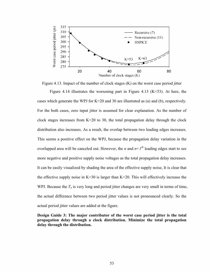
53
Figure 4.13. Impact of the number of clock stages (K) on the worst case period jitter
Figure 4.14 illustrates the worsening part in Figure 4.13 (K<53). At here, the
cases which generate the WPJ for K=20 and 30 are illustrated as (a) and (b), respectively.
For the both cases, zero input jitter is assumed for clear explanation. As the number of
clock stages increases from K=20 to 30, the total propagation delay through the clock
distribution also increases. As a result, the overlap between two leading edges increases.
This seems a positive effect on the WPJ, because the propagation delay variation in the
overlapped area will be canceled out. However, the n and n+1th leading edges start to see
more negative and positive supply noise voltages as the total propagation delay increases.
It can be easily visualized by shading the area of the effective supply noise, It is clear that
the effective supply noise in K=30 is larger than K=20. This will effectively increase the
WPJ. Because the Tn is very long and period jitter changes are very small in terms of time,
the actual difference between two period jitter values is not pronounced clearly. So the
actual period jitter values are added at the figure.
Design Guide 3: The major contributor of the worst case period jitter is the total propagation delay through a clock distribution. Minimize the total propagation delay through the distribution.
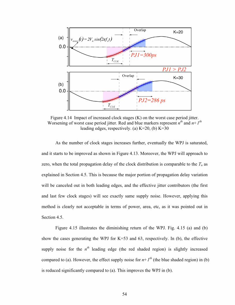
54
Figure 4.14 Impact of increased clock stages (K) on the worst case period jitter. Worsening of worst case period jitter. Red and blue markers represent nth and n+1th
leading edges, respectively. (a) K=20, (b) K=30
As the number of clock stages increases further, eventually the WPJ is saturated,
and it starts to be improved as shown in Figure 4.13. Moreover, the WPJ will approach to
zero, when the total propagation delay of the clock distribution is comparable to the Tn as
explained in Section 4.5. This is because the major portion of propagation delay variation
will be canceled out in both leading edges, and the effective jitter contributors (the first
and last few clock stages) will see exactly same supply noise. However, applying this
method is clearly not acceptable in terms of power, area, etc, as it was pointed out in
Section 4.5.
Figure 4.15 illustrates the diminishing return of the WPJ. Fig. 4.15 (a) and (b)
show the cases generating the WPJ for K=53 and 63, respectively. In (b), the effective
supply noise for the nth leading edge (the red shaded region) is slightly increased
compared to (a). However, the effect supply noise for n+1th (the blue shaded region) in (b)
is reduced significantly compared to (a). This improves the WPJ in (b).
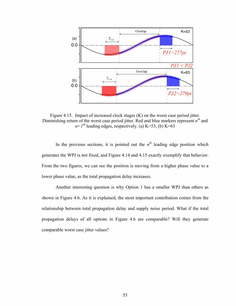
55
Figure 4.15. Impact of increased clock stages (K) on the worst case period jitter. Diminishing return of the worst case period jitter. Red and blue markers represent nth and
n+1th leading edges, respectively. (a) K=53, (b) K=63
In the previous sections, it is pointed out the nth leading edge position which
generates the WPJ is not fixed, and Figure 4.14 and 4.15 exactly exemplify that behavior.
From the two figures, we can see the position is moving from a higher phase value to a
lower phase value, as the total propagation delay increases.
Another interesting question is why Option 1 has a smaller WPJ than others as
shown in Figure 4.6. As it is explained, the most important contribution comes from the
relationship between total propagation delay and supply noise period. What if the total
propagation delays of all options in Figure 4.6 are comparable? Will they generate
comparable worst case jitter values?
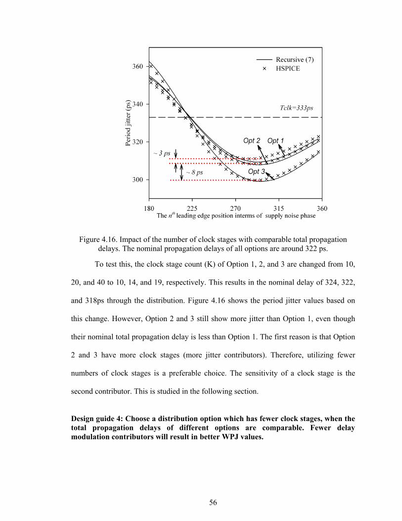
56
Figure 4.16. Impact of the number of clock stages with comparable total propagation delays. The nominal propagation delays of all options are around 322 ps.
To test this, the clock stage count (K) of Option 1, 2, and 3 are changed from 10,
20, and 40 to 10, 14, and 19, respectively. This results in the nominal delay of 324, 322,
and 318ps through the distribution. Figure 4.16 shows the period jitter values based on
this change. However, Option 2 and 3 still show more jitter than Option 1, even though
their nominal total propagation delay is less than Option 1. The first reason is that Option
2 and 3 have more clock stages (more jitter contributors). Therefore, utilizing fewer
numbers of clock stages is a preferable choice. The sensitivity of a clock stage is the
second contributor. This is studied in the following section.
Design guide 4: Choose a distribution option which has fewer clock stages, when the total propagation delays of different options are comparable. Fewer delay modulation contributors will result in better WPJ values.
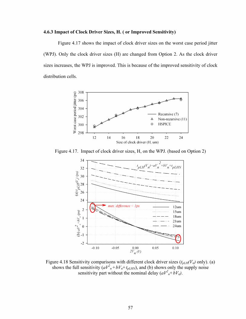
57
4.6.3 Impact of Clock Driver Sizes, H. ( or Improved Sensitivity)
Figure 4.17 shows the impact of clock driver sizes on the worst case period jitter
(WPJ). Only the clock driver sizes (H) are changed from Option 2. As the clock driver
sizes increases, the WPJ is improved. This is because of the improved sensitivity of clock
distribution cells.
Figure 4.17. Impact of clock driver sizes, H, on the WPJ. (based on Option 2)
Figure 4.18 Sensitivity comparisons with different clock driver sizes (tpLH(Vn) only). (a) shows the full sensitivity (aV2
n +bVn+tpLHN), and (b) shows only the supply noise sensitivity part without the nominal delay (aV2
n+bVn).
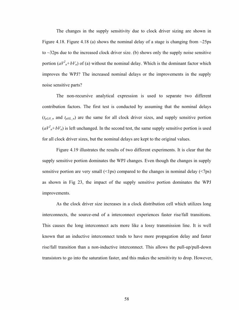
58
The changes in the supply sensitivity due to clock driver sizing are shown in
Figure 4.18. Figure 4.18 (a) shows the nominal delay of a stage is changing from ~25ps
to ~32ps due to the increased clock driver size. (b) shows only the supply noise sensitive
portion (aV2n+bVn) of (a) without the nominal delay. Which is the dominant factor which
improves the WPJ? The increased nominal delays or the improvements in the supply
noise sensitive parts?
The non-recursive analytical expression is used to separate two different
contribution factors. The first test is conducted by assuming that the nominal delays
(tpLH_n and tpHL_n) are the same for all clock driver sizes, and supply sensitive portion
(aV2n+bVn) is left unchanged. In the second test, the same supply sensitive portion is used
for all clock driver sizes, but the nominal delays are kept to the original values.
Figure 4.19 illustrates the results of two different experiments. It is clear that the
supply sensitive portion dominates the WPJ changes. Even though the changes in supply
sensitive portion are very small (<1ps) compared to the changes in nominal delay (<7ps)
as shown in Fig 23, the impact of the supply sensitive portion dominates the WPJ
improvements.
As the clock driver size increases in a clock distribution cell which utilizes long
interconnects, the source-end of a interconnect experiences faster rise/fall transitions.
This causes the long interconnect acts more like a lossy transmission line. It is well
known that an inductive interconnect tends to have more propagation delay and faster
rise/fall transition than a non-inductive interconnect. This allows the pull-up/pull-down
transistors to go into the saturation faster, and this makes the sensitivity to drop. However,
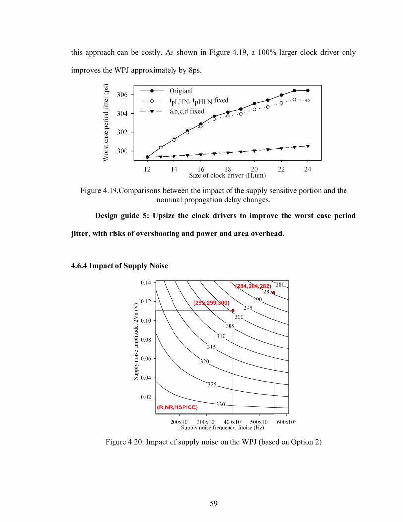
59
this approach can be costly. As shown in Figure 4.19, a 100% larger clock driver only
improves the WPJ approximately by 8ps.
Figure 4.19.Comparisons between the impact of the supply sensitive portion and the nominal propagation delay changes.
Design guide 5: Upsize the clock drivers to improve the worst case period
jitter, with risks of overshooting and power and area overhead.
4.6.4 Impact of Supply Noise
Figure 4.20. Impact of supply noise on the WPJ (based on Option 2)
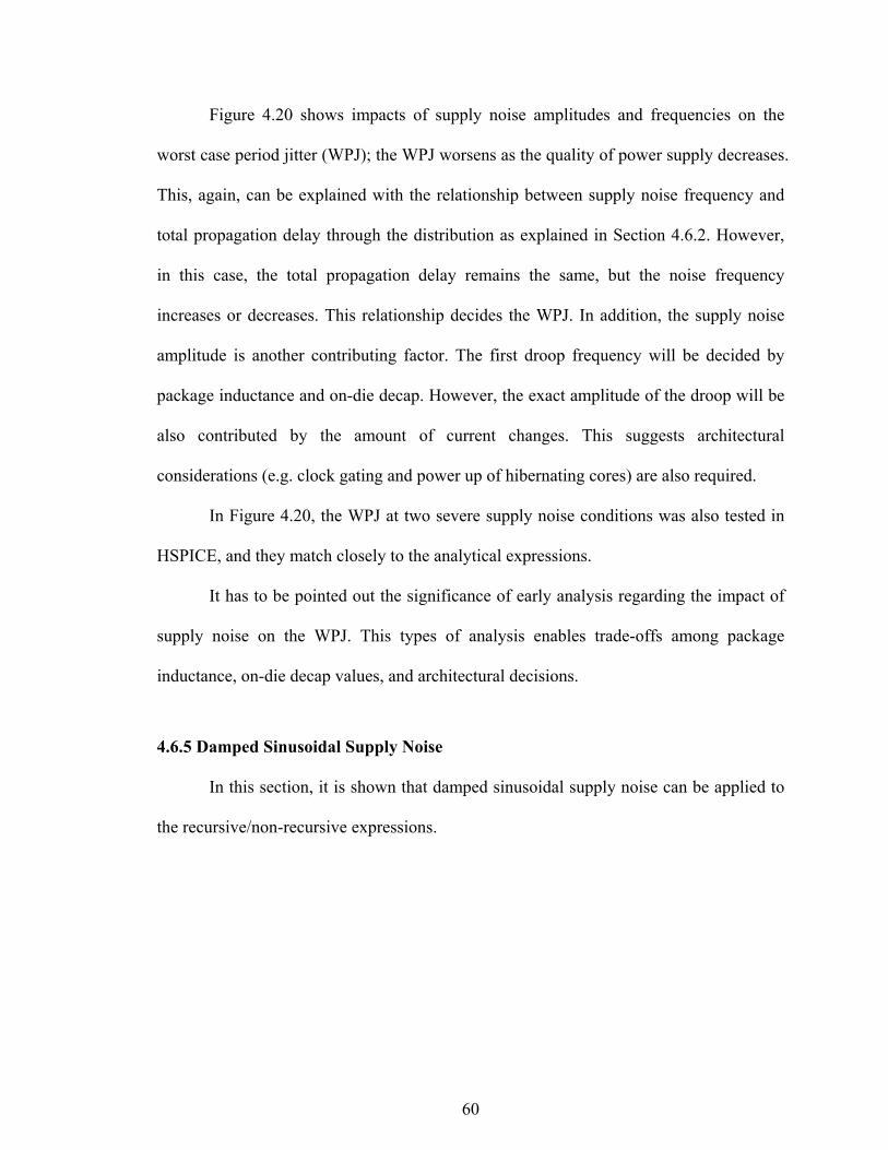
60
Figure 4.20 shows impacts of supply noise amplitudes and frequencies on the
worst case period jitter (WPJ); the WPJ worsens as the quality of power supply decreases.
This, again, can be explained with the relationship between supply noise frequency and
total propagation delay through the distribution as explained in Section 4.6.2. However,
in this case, the total propagation delay remains the same, but the noise frequency
increases or decreases. This relationship decides the WPJ. In addition, the supply noise
amplitude is another contributing factor. The first droop frequency will be decided by
package inductance and on-die decap. However, the exact amplitude of the droop will be
also contributed by the amount of current changes. This suggests architectural
considerations (e.g. clock gating and power up of hibernating cores) are also required.
In Figure 4.20, the WPJ at two severe supply noise conditions was also tested in
HSPICE, and they match closely to the analytical expressions.
It has to be pointed out the significance of early analysis regarding the impact of
supply noise on the WPJ. This types of analysis enables trade-offs among package
inductance, on-die decap values, and architectural decisions.
4.6.5 Damped Sinusoidal Supply Noise
In this section, it is shown that damped sinusoidal supply noise can be applied to
the recursive/non-recursive expressions.
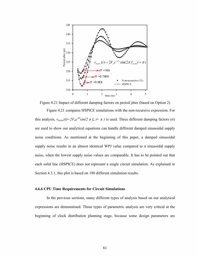
61
Figure 4.21 Impact of different damping factors on period jitter (based on Option 2)
Figure 4.21 compares HSPICE simulations with the non-recursive expression. For
this analysis, vnoise(t)=2Vne-σtsin(2 π fn t+ π ) is used. Three different damping factors (σ)
are used to show our analytical equations can handle different damped sinusoidal supply
noise conditions. As mentioned at the beginning of this paper, a damped sinusoidal
supply noise results in an almost identical WPJ value compared to a sinusoidal supply
noise, when the lowest supply noise values are comparable. It has to be pointed out that
each solid line (HSPICE) does not represent a single circuit simulation. As explained in
Section 4.3.1, this plot is based on 180 different simulation results.
4.6.6 CPU Time Requirements for Circuit Simulations
In the previous sections, many different types of analysis based on our analytical
expressions are demonstraed. Those types of parametric analysis are very critical at the
beginning of clock distribution planning stage, because some design parameters are
62
unknown or undecided at that stage. To assure the quality of a clock distribution, a wide
range of different design parameters have to be evaluated as quickly as possible.
Table 4.2 shows an estimate of CPU time requirements for analytical equations
and HSPICE based simulations to find the worst case period jitter in a reasonably wide
design space. For a fair comparison, a 2GHz CPU setting was assumed. The comparison
shows that purely relying on circuit simulations is extremely costly. Even if we assume a
multirate simulator can reduce the required CPU time by 80% per simulation, still it
requires 18.75 days to finish all the simulations. In this condition, (15) can play a
valuable role, because the expression can guide the circuit simulations to finish the
required simulations in reduced time. For a multirate simulator, the required CPU time
can be further reduced to 5.6 days
Table 4.2. CPU time comparison for WPJ search
Analytical equation HSPICE BA* NA *NF*CF*TO*CO*VS*IJ
+BS*TO*CO*VS
(BH*I)* NA*NF*CF*TO*CO*VS*IJ
2.45 hours 93.75 days
Symbol Description Default BA Base line CPU time of analytical equations (<1 s) 1 s BH Base line CPU time of a HSPICE based circuit simulation
(60<BH<500 s) 100 s
BS Base line CPU time of a HSPICE based sensitivity test (<20 s) 20 s I # of simulation iteration to find the WPJ 10 NA # of different noise amplitudes 5 NF # of different noise frequencies 5 CF # of different clock frequencies for frequency scaling 3 TO # of different distribution options under consideration 4 CO # of different simulation corners 3 IJ # of different input jitter assumption 3 VS # of different voltage steps for voltage scaling 3
63
4.7 Case Study: Putting Everything Together for Clock Data Compensation (Active Jitter Mitigation Based on VCO Voltage Modulation)
In this section, our analytical equations are used to demonstrate how Clock Data
Compensation (CDC) [2] can be easily studied without timing consuming circuit
simulations. This is because our expression can give accurate predictions and they can
handle input jitter from other sources (e.g PLL).
CDC is in nature hard to explain in a short sentence. However, the main idea is
avoiding the worst case period jitter (WPJ) when the critical paths of a microprocessor
experience their worst delay to avoid the timing failures. Also, possibly it improves the
circuit performance by utilizing power supply modulated clock jitter.
There have been different approaches to mitigate and utilize clock jitter. [8] [10]
[22] [23]. Here, it is assumed that a Voltage Controlled Oscillator (VCO) inside an
adaptive PLL senses digital supply fluctuation as presented in Nehalem [10].
To study the impact of an Adaptive PLL (supply noise modulated VCO), a
mathematical model of the VCO without random jitter is modeled, and the same model is
implemented in Verilog-A for circuit simulations, and this was simulated with Option 2.
The simulation results are shown in Figure 4.22.
The center frequency of the VCO is assumed to be 3GHz, and the tuning range
due to the supply noise is assumed to be from 2.7GHz to 3.3GHz, when the supply noises
are at the lowest and the highest point, respectively. Also the phase accumulation inside
the VCO can be random value (Figure 4.22 is the case of zero initial phase
accumulation).The power supply noise is modeled as a damped sinusoidal waveform as
shown in Figure 4.22 (b)
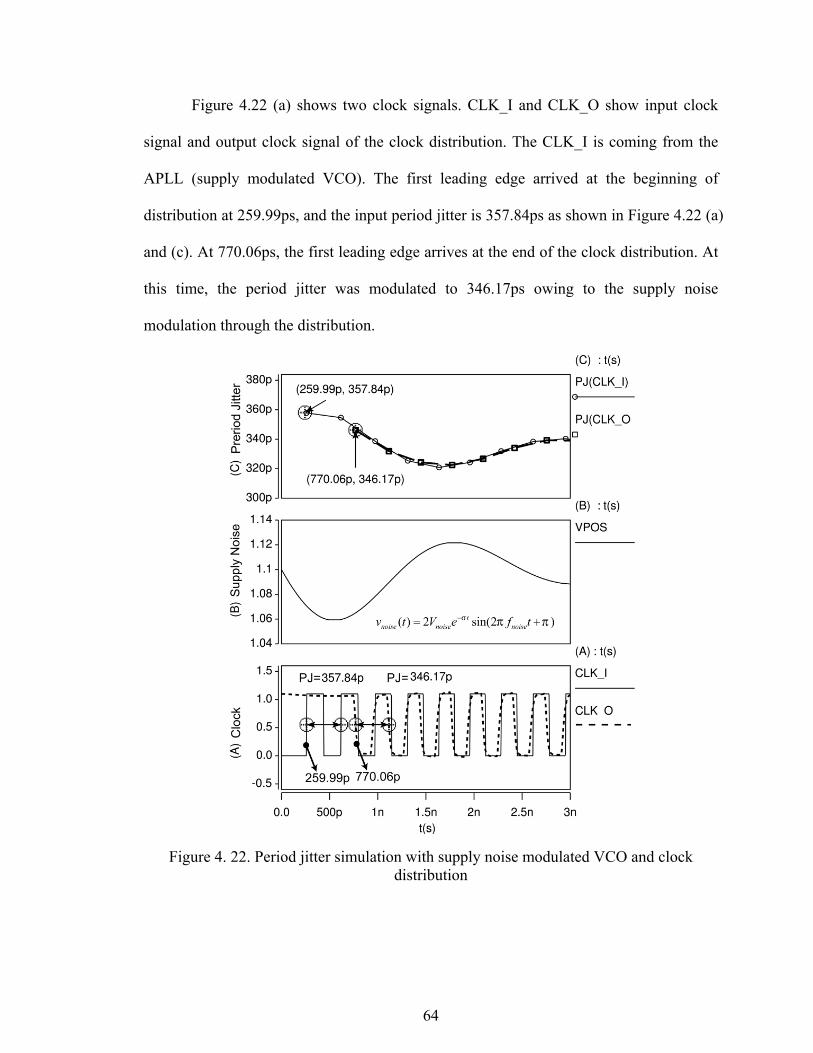
64
Figure 4.22 (a) shows two clock signals. CLK_I and CLK_O show input clock
signal and output clock signal of the clock distribution. The CLK_I is coming from the
APLL (supply modulated VCO). The first leading edge arrived at the beginning of
distribution at 259.99ps, and the input period jitter is 357.84ps as shown in Figure 4.22 (a)
and (c). At 770.06ps, the first leading edge arrives at the end of the clock distribution. At
this time, the period jitter was modulated to 346.17ps owing to the supply noise
modulation through the distribution.
Figure 4. 22. Period jitter simulation with supply noise modulated VCO and clock distribution
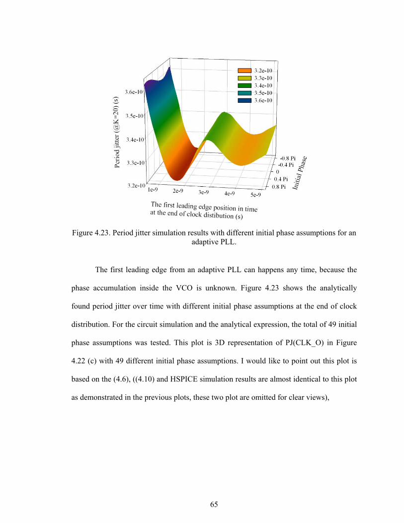
65
Figure 4.23. Period jitter simulation results with different initial phase assumptions for an adaptive PLL.
The first leading edge from an adaptive PLL can happens any time, because the
phase accumulation inside the VCO is unknown. Figure 4.23 shows the analytically
found period jitter over time with different initial phase assumptions at the end of clock
distribution. For the circuit simulation and the analytical expression, the total of 49 initial
phase assumptions was tested. This plot is 3D representation of PJ(CLK_O) in Figure
4.22 (c) with 49 different initial phase assumptions. I would like to point out this plot is
based on the (4.6), ((4.10) and HSPICE simulation results are almost identical to this plot
as demonstrated in the previous plots, these two plot are omitted for clear views),
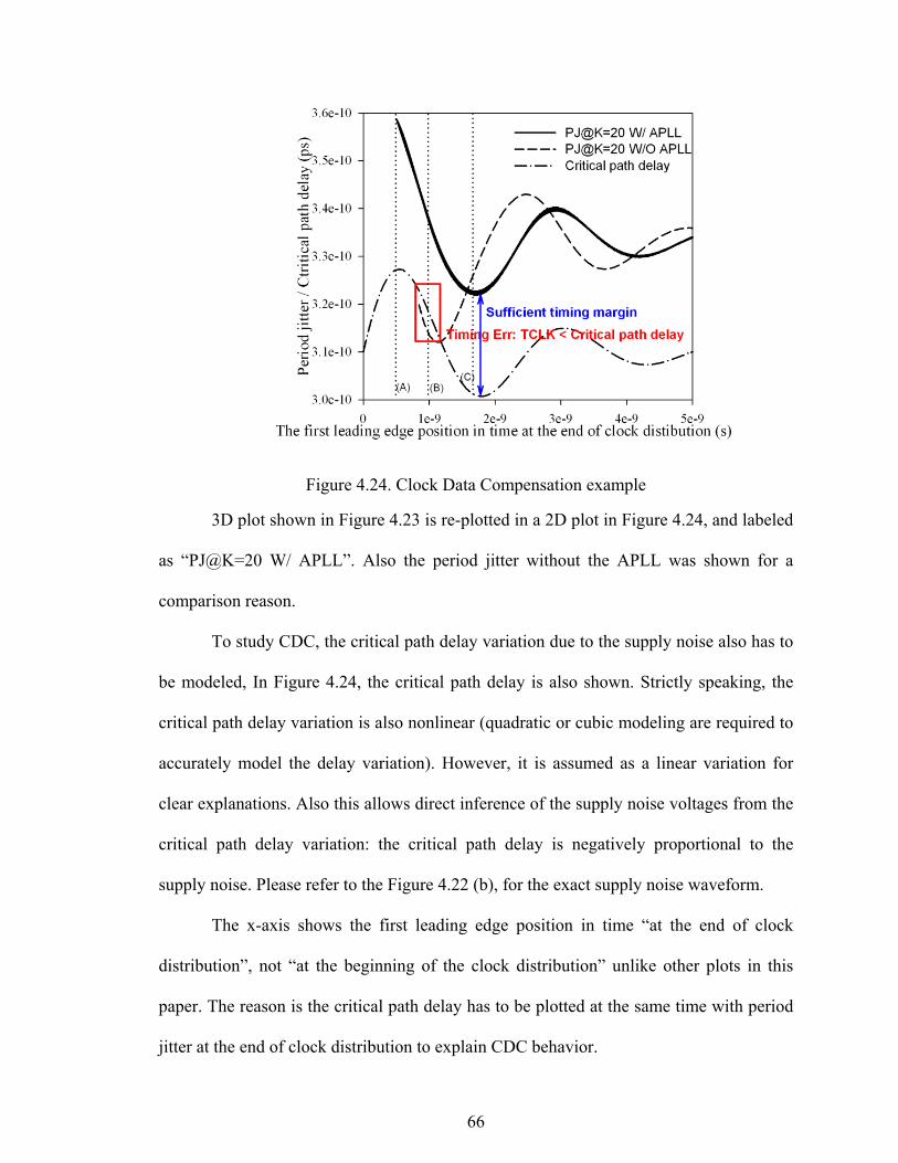
66
Figure 4.24. Clock Data Compensation example
3D plot shown in Figure 4.23 is re-plotted in a 2D plot in Figure 4.24, and labeled
as “PJ@K=20 W/ APLL”. Also the period jitter without the APLL was shown for a
comparison reason.
To study CDC, the critical path delay variation due to the supply noise also has to
be modeled, In Figure 4.24, the critical path delay is also shown. Strictly speaking, the
critical path delay variation is also nonlinear (quadratic or cubic modeling are required to
accurately model the delay variation). However, it is assumed as a linear variation for
clear explanations. Also this allows direct inference of the supply noise voltages from the
critical path delay variation: the critical path delay is negatively proportional to the
supply noise. Please refer to the Figure 4.22 (b), for the exact supply noise waveform.
The x-axis shows the first leading edge position in time “at the end of clock
distribution”, not “at the beginning of the clock distribution” unlike other plots in this
paper. The reason is the critical path delay has to be plotted at the same time with period
jitter at the end of clock distribution to explain CDC behavior.
67
As the supply noise starts to drop, the VCO starts to accumulate the phase, and
the critical path delay starts to increase. At time (A), the total period jitter will have the
longest clock period due to the longest input jitter from the APLL and the critical path
delay also reaches to the worst case condition. The reason is simply the supply voltage is
at the lowest point. After time (A), the clock period at the end of the distribution starts to
decreases, because the VCO starts to see higher supply voltage than before. Also the
critical path delay starts to decrease. However the margin between the APLL based clock
period and the critical path delay is sufficient enough to sustain correct circuit operation.
In the case of period jitter without APLL, the timing failure happens around time (B). At
time (C), the period jitter with APLL shows the worst case period jitter, but the critical
path delay was also reduced, because the supply noise now has a positive value. As a
result, there is sufficient timing margin. This clearly demonstrates the impact of APLL on
active period jitter reduction. This implies that the nominal clock period can be decreased
by ~15 ps.
This case study uses a fixed center frequency and tuning range to show the CDC
behavior. In real clock generation / distribution design, finding optimal parameters for
them will be an extremely difficult challenge, when the CDC is considered with other
design parameters described in the previous sections. With the help of our fast and
accurate analytical expressions, the clock generation / distribution design can quickly
reach at its mature stage.
68
4.8 Conclusion
Novel period jitter expressions are formulated for global binary clock trees while
considering the details of different clock distribution parameters and time varying supply
noise. Also, the period jitter behavior in global binary clock tree is extensively analyzed
with many examples to provide insight into period jitter induced by the first droop. Based
on our experiments, detailed guidelines for clock distribution design are suggested.
69
CHAPTER 5
POWER SUPPLY DROP AND ON-DIE DROOP DETECTOR
This paper presents a new design of supply droop detector system with a 10-
20mV resolution at a very fast sampling rate (3GHz) in IBM 45nm SOI process. The
detector system samples noisy supply voltage and stable reference voltages, and these
sampled voltages are converted into different propagation delay values by using current
starved inverters. Simple arbiters are used to convert these propagation delay differences
into digitally reconstructed supply droop voltage. In addition, the detector has only 1
clock latency; a digital value of supply droop voltage is available after one clock cycle.
This new droop detector system can greatly assist an adaptive frequency scaling system
with a digital control and short latency.
5.1 Introduction
With greatly increased current density and reduced supply voltage of high-end
microprocessors, the supply droop starts to limit the maximum operating frequency.
There have been several different approaches to tackle this problem. One trend is
measuring the supply noise on a die to verify the quality of the supply distribution
network and reusing this information to build more robust supply distribution networks.
These approaches mainly focused on accurate (high resolution) and wide bandwidth
measurements [38] [39] [40] [41]. Another trend is actively suppressing and
compensating power supply droop. This can also be categorized into two methodologies.
The first one is direct injection of current to the problematic nodes [42]. This approach
can be effective to a localized droop, but it might not be an effective solution for a
70
globally shared supply droop. The second one is dynamic adjustment of clock frequency
to avoid timing failure due to the supply droop [8] [10] [43].
For the dynamic supply droop compensations based on the adjustment of clock
period, fast (preferably one clock cycle) detection is critical. This is because of the
relationship between power supply noise frequency and clock frequency, as explained in
Section 5.2. However, the latency of supply droop detection in [38] [39] [40] [41] is very
high, because they aimed at measuring accurate supply noise. Some of them require
many samples of measurements to establish the accurate representation of supply noise
owing to their cyclostationary process assumption. [8] and [10] can react to the droop
within a clock cycle, but they cannot be used to reconstruct the supply noise from their
measurements. [10] mixes noisy digital supply and stable analog supply to change the
clock frequency of VCO. [8] detects propagation delay variations in delay lines. [43] can
achieve reasonable droop detection with reasonable latency, but it requires massive
analog circuit design. Recently [44] presented a voltage detection scheme which can
generates voltage droop detection with 10~15mv resolution for DFX purposes.
In this work, the following features are targeted for our droop detector system: 1)
10-20mV resolution, 2) one clock cycle latency, 3) low power consumption, and 4)
digital outputs. The digital output capability is one of the most important design targets of
our design, because it will enable logging capability of power supply noise. The logged
data can be used in architecture based prediction schemes [45]. However, the major target
of this work is assisting an adaptive clocking system.
Section 5.2 describes a power delivery network model, which is generated from
openly accessible power delivery models of server class motherboard design
71
specifications and the impedance profile of Intel Nehalem. The specifications for our
droop detector system were derived from the study on the power delivery model. The
detailed explanation about the droop detector system is presented in Section 5.3, and the
simulation results considering arbiter metastability and process variation are presented in
Section 5.4. The test chip implementation of our droop detector system is illustrated in
Section 5.5 with a post layout simulation result based on the full parasitic extraction of
the droop detector system.
5.2 Power Delivery Network
This section describes a power delivery network that captures impedance
components at board, package, and die level. This work is based on three available
publications from Intel Corporation [34] [46] [47].
Figure 5.1 illustrates a simplified power delivery model. A Voltage Regulator
Module (VRM) is the main source of the delivery system, and there are many decoupling
capacitors on the board, socket, package, and on-die level. Owing to the capacitance
imperfection, effective parasitic series resistances and inductances (ESR and ESL) also
appear in the power delivery network. Intrinsic/extrinsic on-die decoupling capacitors
help reduce the impedance of the supply delivery network. However, the on-die
capacitors can react to the package inductance, and this can generate impedance
imperfection at a certain frequency range, as shown in Figure 5.2.
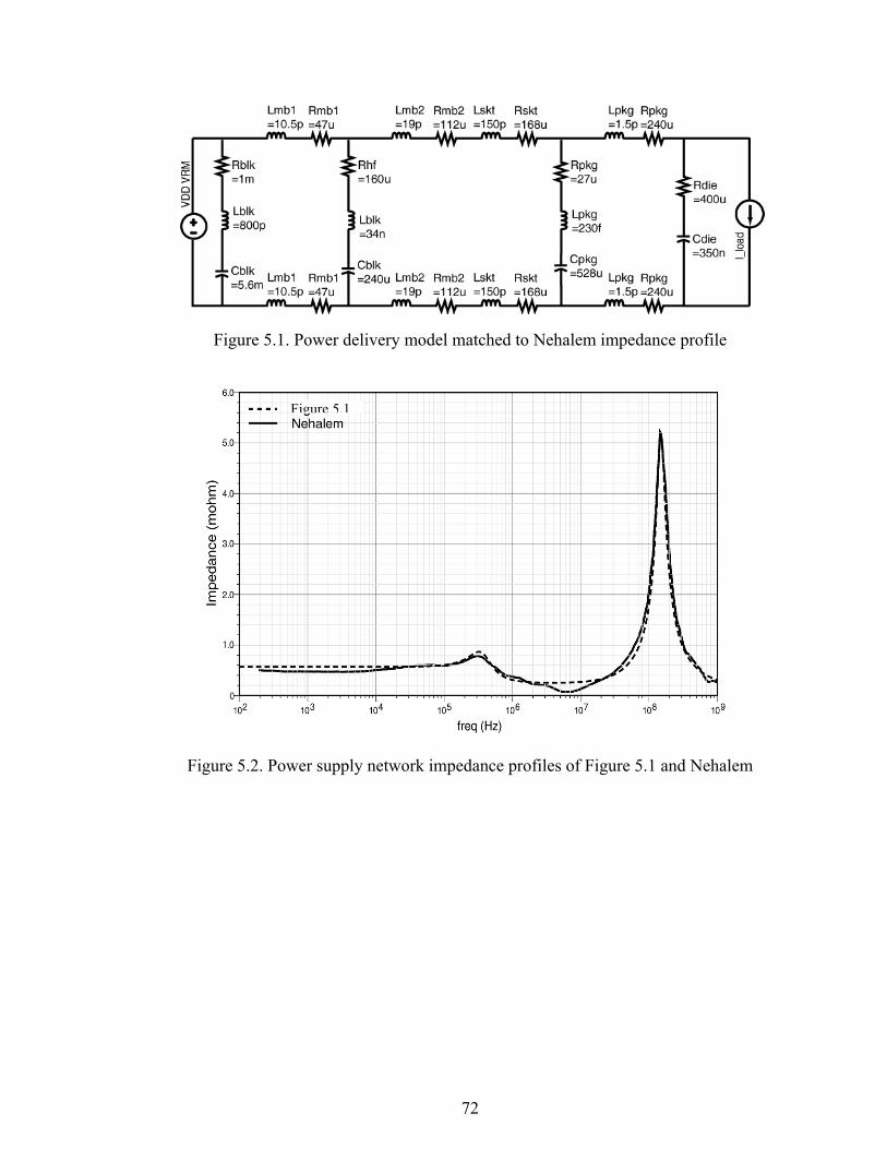
72
Figure 5.1. Power delivery model matched to Nehalem impedance profile
Figure 5.2. Power supply network impedance profiles of Figure 5.1 and Nehalem
Figure 5.1
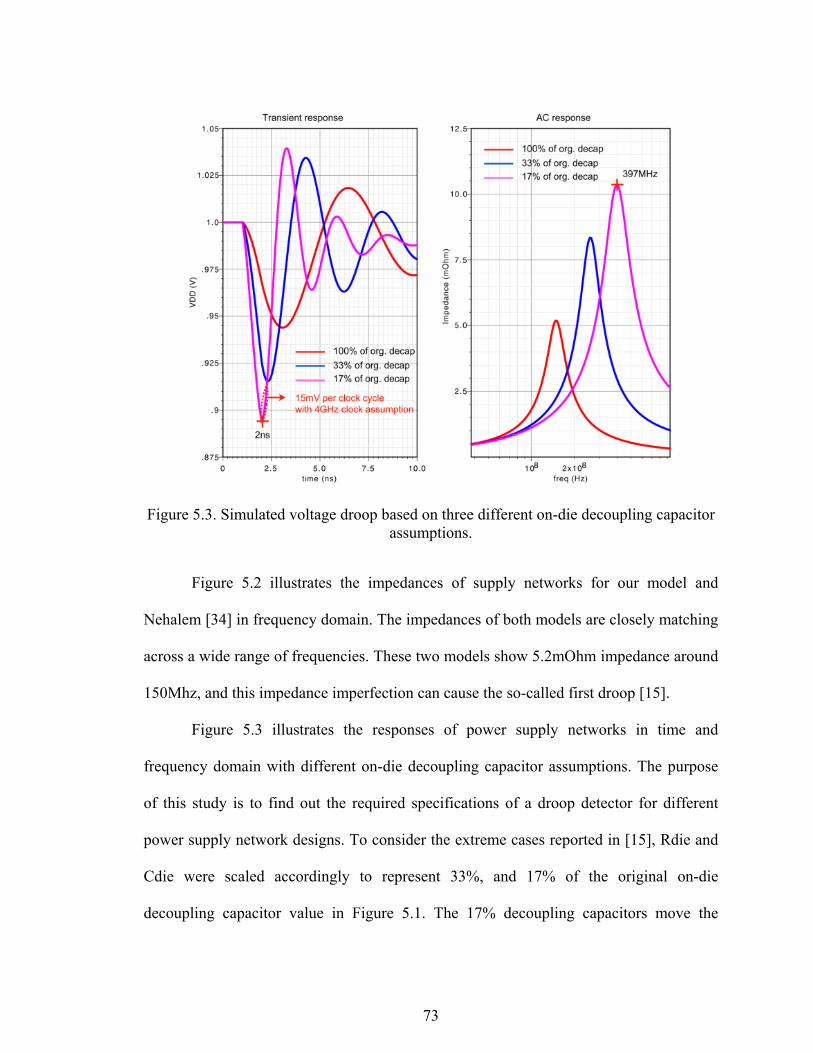
73
Figure 5.3. Simulated voltage droop based on three different on-die decoupling capacitor assumptions.
Figure 5.2 illustrates the impedances of supply networks for our model and
Nehalem [34] in frequency domain. The impedances of both models are closely matching
across a wide range of frequencies. These two models show 5.2mOhm impedance around
150Mhz, and this impedance imperfection can cause the so-called first droop [15].
Figure 5.3 illustrates the responses of power supply networks in time and
frequency domain with different on-die decoupling capacitor assumptions. The purpose
of this study is to find out the required specifications of a droop detector for different
power supply network designs. To consider the extreme cases reported in [15], Rdie and
Cdie were scaled accordingly to represent 33%, and 17% of the original on-die
decoupling capacitor value in Figure 5.1. The 17% decoupling capacitors move the
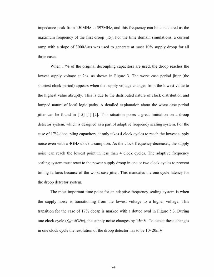
74
impedance peak from 150MHz to 397MHz, and this frequency can be considered as the
maximum frequency of the first droop [15]. For the time domain simulations, a current
ramp with a slope of 3000A/us was used to generate at most 10% supply droop for all
three cases.
When 17% of the original decoupling capacitors are used, the droop reaches the
lowest supply voltage at 2ns, as shown in Figure 3. The worst case period jitter (the
shortest clock period) appears when the supply voltage changes from the lowest value to
the highest value abruptly. This is due to the distributed nature of clock distribution and
lumped nature of local logic paths. A detailed explanation about the worst case period
jitter can be found in [15] [1] [2]. This situation poses a great limitation on a droop
detector system, which is designed as a part of adaptive frequency scaling system. For the
case of 17% decoupling capacitors, it only takes 4 clock cycles to reach the lowest supply
noise even with a 4GHz clock assumption. As the clock frequency decreases, the supply
noise can reach the lowest point in less than 4 clock cycles. The adaptive frequency
scaling system must react to the power supply droop in one or two clock cycles to prevent
timing failures because of the worst case jitter. This mandates the one cycle latency for
the droop detector system.
The most important time point for an adaptive frequency scaling system is when
the supply noise is transitioning from the lowest voltage to a higher voltage. This
transition for the case of 17% decap is marked with a dotted oval in Figure 5.3. During
one clock cycle (fclk=4GHz), the supply noise changes by 15mV. To detect these changes
in one clock cycle the resolution of the droop detector has to be 10~20mV.
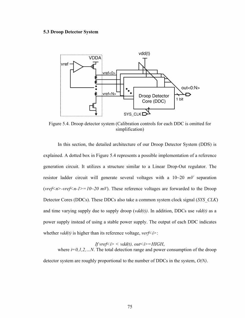
75
5.3 Droop Detector System
Figure 5.4. Droop detector system (Calibration controls for each DDC is omitted for simplification)
In this section, the detailed architecture of our Droop Detector System (DDS) is
explained. A dotted box in Figure 5.4 represents a possible implementation of a reference
generation circuit. It utilizes a structure similar to a Linear Drop-Out regulator. The
resistor ladder circuit will generate several voltages with a 10~20 mV separation
(vref<n>-vref<n-1>=10~20 mV). These reference voltages are forwarded to the Droop
Detector Cores (DDCs). These DDCs also take a common system clock signal (SYS_CLK)
and time varying supply due to supply droop (vdd(t)). In addition, DDCs use vdd(t) as a
power supply instead of using a stable power supply. The output of each DDC indicates
whether vdd(t) is higher than its reference voltage, verf<i>:
If vref<i> < vdd(t), out<i>=HIGH, where i=0,1,2,…N. The total detection range and power consumption of the droop
detector system are roughly proportional to the number of DDCs in the system, O(N).
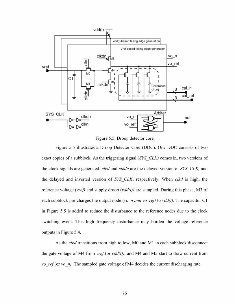
76
Figure 5.5. Droop detector core
Figure 5.5 illustrates a Droop Detector Core (DDC). One DDC consists of two
exact copies of a subblock. As the triggering signal (SYS_CLK) comes in, two versions of
the clock signals are generated. clkd and clkdn are the delayed version of SYS_CLK, and
the delayed and inverted version of SYS_CLK, respectively. When clkd is high, the
reference voltage (vref) and supply droop (vdd(t)) are sampled. During this phase, M3 of
each subblock pre-charges the output node (vo_n and vo_ref) to vdd(t). The capacitor C1
in Figure 5.5 is added to reduce the disturbance to the reference nodes due to the clock
switching event. This high frequency disturbance may burden the voltage reference
outputs in Figure 5.4.
As the clkd transitions from high to low, M0 and M1 in each subblock disconnect
the gate voltage of M4 from vref (or vdd(t)), and M4 and M5 start to draw current from
vo_ref (or vo_n). The sampled gate voltage of M4 decides the current discharging rate.
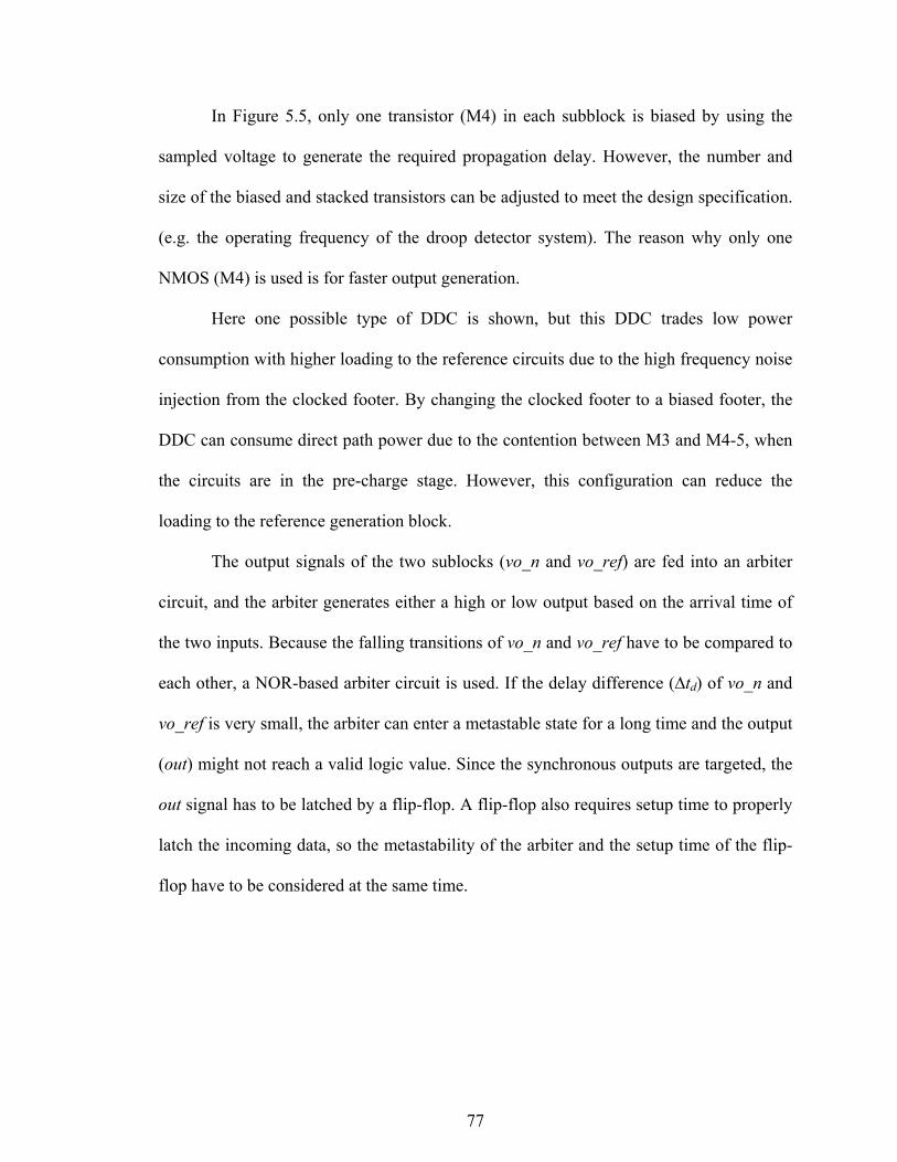
77
In Figure 5.5, only one transistor (M4) in each subblock is biased by using the
sampled voltage to generate the required propagation delay. However, the number and
size of the biased and stacked transistors can be adjusted to meet the design specification.
(e.g. the operating frequency of the droop detector system). The reason why only one
NMOS (M4) is used is for faster output generation.
Here one possible type of DDC is shown, but this DDC trades low power
consumption with higher loading to the reference circuits due to the high frequency noise
injection from the clocked footer. By changing the clocked footer to a biased footer, the
DDC can consume direct path power due to the contention between M3 and M4-5, when
the circuits are in the pre-charge stage. However, this configuration can reduce the
loading to the reference generation block.
The output signals of the two sublocks (vo_n and vo_ref) are fed into an arbiter
circuit, and the arbiter generates either a high or low output based on the arrival time of
the two inputs. Because the falling transitions of vo_n and vo_ref have to be compared to
each other, a NOR-based arbiter circuit is used. If the delay difference (∆td) of vo_n and
vo_ref is very small, the arbiter can enter a metastable state for a long time and the output
(out) might not reach a valid logic value. Since the synchronous outputs are targeted, the
out signal has to be latched by a flip-flop. A flip-flop also requires setup time to properly
latch the incoming data, so the metastability of the arbiter and the setup time of the flip-
flop have to be considered at the same time.
78
Figure 5.6. Simulated waveform of a droop detector core: Near metastable state.
Figure 5.6 exemplifies the operation of a DDC near the metastable state. The out
signal was starting to rise at 7.83ns, but it went down again. For the second transition, the
out signal reached vdd(t) at 8.1ps. In this simulation result, the out signal could escape
from the metastable state with a short delay, but a reduced ∆td can cause the arbiter to
take a very long time to evaluate the output. This concern regarding the metastability is
studied in Section 5.4.1.
To guarantee correct operation of the droop detector system, the following timing
constraint has to be satisfied:
D*Tsys_clk>tp_clk+tp_ddc+tp_arb+tsetup. (5.1)
where tp_clk is the delay from the falling edge of SYS_CLK to clkdn in Figure 5.5,
tp_ddc is the discharging time of a droop detector core, and tp_arb is the time required to
escape the metastable state and to generate a valid logic value. tsetup represents the setup
time of the next stage flip-flop. The addition of all delays has to be less than D*Tsys_clk. D
79
represents the duty cycle of the input clock. In Figure 5.6, a 50% duty cycle is assumed,
but it can be adjusted to compensate long tp_arb.values.
The DDCs are supplied by a non-ideal digital power supply (vdd(t)) as shown in
Figure 5.4 and 5.5. The first and foremost advantage of this approach is that the DDCs do
not require any ideal digital supply voltage for their reliable operation. This implies this
type of droop detector system can be sprinkled across a large die area. Furthermore, the
worst clock jitter happens when the supply noise hits the lowest voltage and transitions to
the higher voltage [15] [25] [1]. During this time, the worst timing margin appears in the
system. This requires the droop detector system to be more sensitive at the lower supply
voltage. Therefore, the delay modulation at a low supply voltage (tp_ddc(vdd_low)) has to
be higher than the delay modulation at a high supply voltage (tp_ddc(vdd_high)). This is
achieved this by utilizing a non-ideal supply (vdd(t)) as the power supply of our DDCs.
This configura-tion guarantees more reliable operation at a low supply voltage because
the DDCs rely on the difference between the two propagation delay modulations in the
subblocks. (Let’s assume a DDC which has the vref of 920mV. When vdd(t) is 900mV,
∆td in Figure 5.6 can be a certain value, ∆td1. When vdd(t) is 940mV, ∆td can be another
value, ∆td2. Even though the difference between vref and vdd(t) is the same value, ∆td1 is
larger than ∆td2.)
One possible problem of this approach is the susceptibility of the gate voltage of
M4 to the high frequency noise component. When the high frequency supply noise
appears in the system, this might cause disruption of the sampled bias voltage at M4. To
prevent this, a passive filtering circuit might be required for some operation conditions of
the droop detector system.
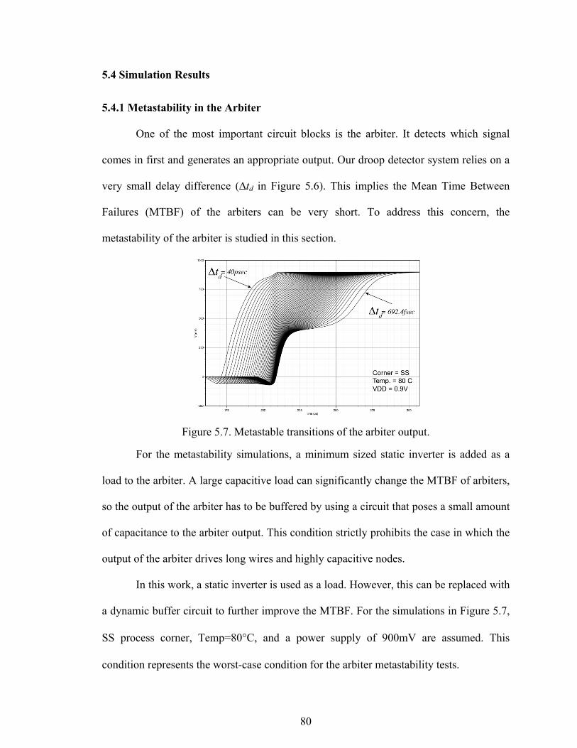
80
5.4 Simulation Results
5.4.1 Metastability in the Arbiter
One of the most important circuit blocks is the arbiter. It detects which signal
comes in first and generates an appropriate output. Our droop detector system relies on a
very small delay difference (∆td in Figure 5.6). This implies the Mean Time Between
Failures (MTBF) of the arbiters can be very short. To address this concern, the
metastability of the arbiter is studied in this section.
Figure 5.7. Metastable transitions of the arbiter output.
For the metastability simulations, a minimum sized static inverter is added as a
load to the arbiter. A large capacitive load can significantly change the MTBF of arbiters,
so the output of the arbiter has to be buffered by using a circuit that poses a small amount
of capacitance to the arbiter output. This condition strictly prohibits the case in which the
output of the arbiter drives long wires and highly capacitive nodes.
In this work, a static inverter is used as a load. However, this can be replaced with
a dynamic buffer circuit to further improve the MTBF. For the simulations in Figure 5.7,
SS process corner, Temp=80°C, and a power supply of 900mV are assumed. This
condition represents the worst-case condition for the arbiter metastability tests.
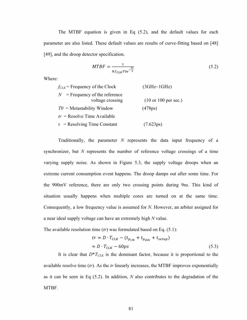
81
The MTBF equation is given in Eq (5.2), and the default values for each
parameter are also listed. These default values are results of curve-fitting based on [48]
[49], and the droop detector specification. = (5.2)
Where:
fCLK = Frequency of the Clock (3GHz~1GHz)
N = Frequency of the reference voltage crossing (10 or 100 per sec.)
T0 = Metastability Window (478ps)
tr = Resolve Time Available
τ = Resolving Time Constant (7.623ps)
Traditionally, the parameter N represents the data input frequency of a
synchronizer, but N represents the number of reference voltage crossings of a time
varying supply noise. As shown in Figure 5.3, the supply voltage droops when an
extreme current consumption event happens. The droop damps out after some time. For
the 900mV reference, there are only two crossing points during 9ns. This kind of
situation usually happens when multiple cores are turned on at the same time.
Consequently, a low frequency value is assumed for N. However, an arbiter assigned for
a near ideal supply voltage can have an extremely high N value.
The available resolution time (tr) was formulated based on Eq. (5.1): = ∙ − ( + + ) ≈ ∙ − 60 (5.3)
It is clear that D*TCLK is the dominant factor, because it is proportional to the
available resolve time (tr). As the tr linearly increases, the MTBF improves exponentially
as it can be seen in Eq (5.2). In addition, N also contributes to the degradation of the
MTBF.
82
Figure 5.8. MTBF of an arbiter circuit. (N=10 and 100, D = 0.5, 0.6, and 07)
Figure 5.9. Dual DDC structure for improved MBTF.
The MTBF with several different assumptions is plotted in Figure 5.8, and this
suggests that achieving 10 years of MTBF is very challenging for a high clock frequency
operation.
The observation in this section leads to many different methods which can
improve MTBF: 1) reducing the load at the arbiter output, 2) removing the DDCs for near
ideal supply detection, 3) reducing the clock frequency slightly, 4) utilizing pulsed
83
clocking or a distorted duty cycle clocking, 5) addition of multi stage synchronizer, and 6)
metastability detector similar to Razor [50].
Figure 5.9 illustrated a dual DDC structure to improve MTBF of the original
design. This structure utilizes pulsed clocking and a doubled clock frequency of
SYS_CLK. With this configuration, MTBF can be improved to 8.7E+6 years even with
N=400MHz assumption.
5.4.2 Monte Carlo Yield Analysis of A Droop Detector Core (DDC)
Process variation on Droop Detector Cores (DDCs) is also one of the most
important issues. If the process variation is severe, correct operation of a DDC has to be
ensured by a calibration mechanism. To study the impact of process variation and
effectiveness of the calibration, several sets of 500 Monte Carlo (MC) runs are simulated
based on the process variation models from IBM 45nm PDK.
To decide a reasonable number of MC runs, propagation delays of one subblock
in Figure 5.5 are measured with different numbers of MC runs. Figure 5.10 (A), (B), and
(C) show impact of 100, 200, and 500 MC runs on the CDF of propagation delay. The red
and blue line in each figure represent two different sampling algorithms. The red line
represents a crude random sampling method, and the blue line represents a Latin
Hypercube sampling method [51]. Variation models are supported by IBM45nm PDK ,
and crude random and Latin Hypercube sampling methods are supported by Cadence
Spectre.
For a small number of samples, Latin Hypercube Sampling (LHS) is showing
better CDF than crude random sampling. As the sample counts increases, both sampling
methods shows similar trend in their CDFs.
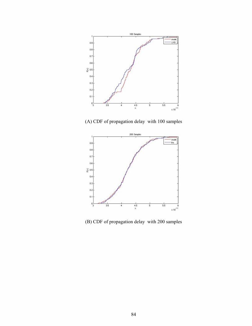
84
(A) CDF of propagation delay with 100 samples
(B) CDF of propagation delay with 200 samples
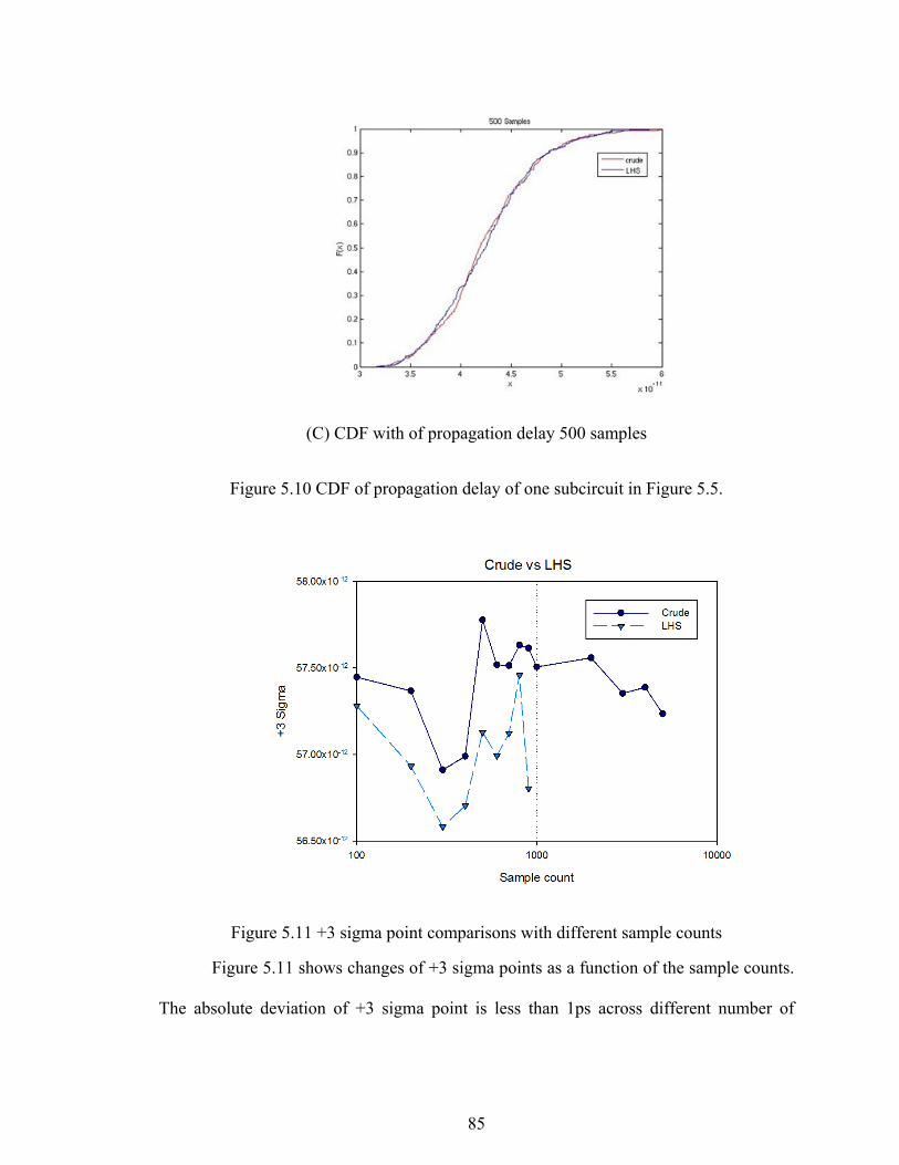
85
(C) CDF with of propagation delay 500 samples
Figure 5.10 CDF of propagation delay of one subcircuit in Figure 5.5.
Figure 5.11 +3 sigma point comparisons with different sample counts
Figure 5.11 shows changes of +3 sigma points as a function of the sample counts.
The absolute deviation of +3 sigma point is less than 1ps across different number of

86
samples. Based on Figure 5.10 and 5.11, a reasonable sample count was decided to be
500 samples.
The Monte Carlo simulations are designed to check whether the process variation
can be calibrated. The vref of a DDC core was set to the nominal supply voltage (1V). At
9 different vdd(t) corners, 500 MC runs are simulated without any calibration setting.
This is equivalent to 4500 single simulations. The simulation results are post-processed
with a measurement script which checks whether the DDC evaluated high or not with a
given process variation and vdd(t). In Figure 10, the solid line represents the simulation
results without any calibration. After this, each MC run is re-simulated 6 times to find an
appropriate calibration setting, and this is equivalent to 6 x 4500 single simulations. The
same process was repeated for 3 different temperature corners, and the total simulation
counts were 3 x 6 x 4500= 81000. The results of calibrations are marked with dotted lines
in Figure 5.12.
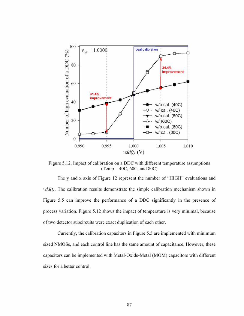
87
Figure 5.12. Impact of calibration on a DDC with different temperature assumptions (Temp = 40C, 60C, and 80C)
The y and x axis of Figure 12 represent the number of “HIGH” evaluations and
vdd(t). The calibration results demonstrate the simple calibration mechanism shown in
Figure 5.5 can improve the performance of a DDC significantly in the presence of
process variation. Figure 5.12 shows the impact of temperature is very minimal, because
of two detector subcircuits were exact duplication of each other.
Currently, the calibration capacitors in Figure 5.5 are implemented with minimum
sized NMOSs, and each control line has the same amount of capacitance. However, these
capacitors can be implemented with Metal-Oxide-Metal (MOM) capacitors with different
sizes for a better control.
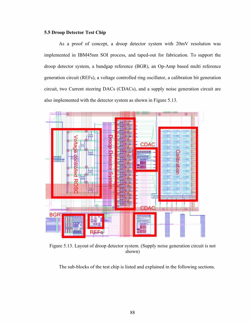
88
5.5 Droop Detector Test Chip
As a proof of concept, a droop detector system with 20mV resolution was
implemented in IBM45nm SOI process, and taped-out for fabrication. To support the
droop detector system, a bandgap reference (BGR), an Op-Amp based multi reference
generation circuit (REFs), a voltage controlled ring oscillator, a calibration bit generation
circuit, two Current steering DACs (CDACs), and a supply noise generation circuit are
also implemented with the detector system as shown in Figure 5.13.
Figure 5.13. Layout of droop detector system. (Supply noise generation circuit is not shown)
The sub-blocks of the test chip is listed and explained in the following sections.
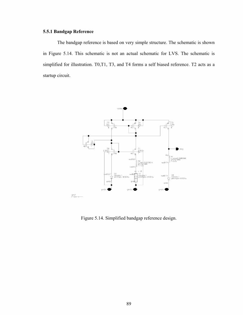
89
5.5.1 Bandgap Reference
The bandgap reference is based on very simple structure. The schematic is shown
in Figure 5.14. This schematic is not an actual schematic for LVS. The schematic is
simplified for illustration. T0,T1, T3, and T4 forms a self biased reference. T2 acts as a
startup circuit.
Figure 5.14. Simplified bandgap reference design.
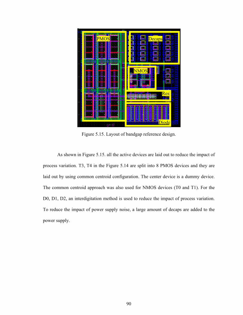
90
Figure 5.15. Layout of bandgap reference design.
As shown in Figure 5.15. all the active devices are laid out to reduce the impact of
process variation. T3, T4 in the Figure 5.14 are split into 8 PMOS devices and they are
laid out by using common centroid configuration. The center device is a dummy device.
The common centroid approach was also used for NMOS devices (T0 and T1). For the
D0, D1, D2, an interdigitation method is used to reduce the impact of process variation.
To reduce the impact of power supply noise, a large amount of decaps are added to the
power supply.
PMOS Decaps
Diode
NMOS
Res
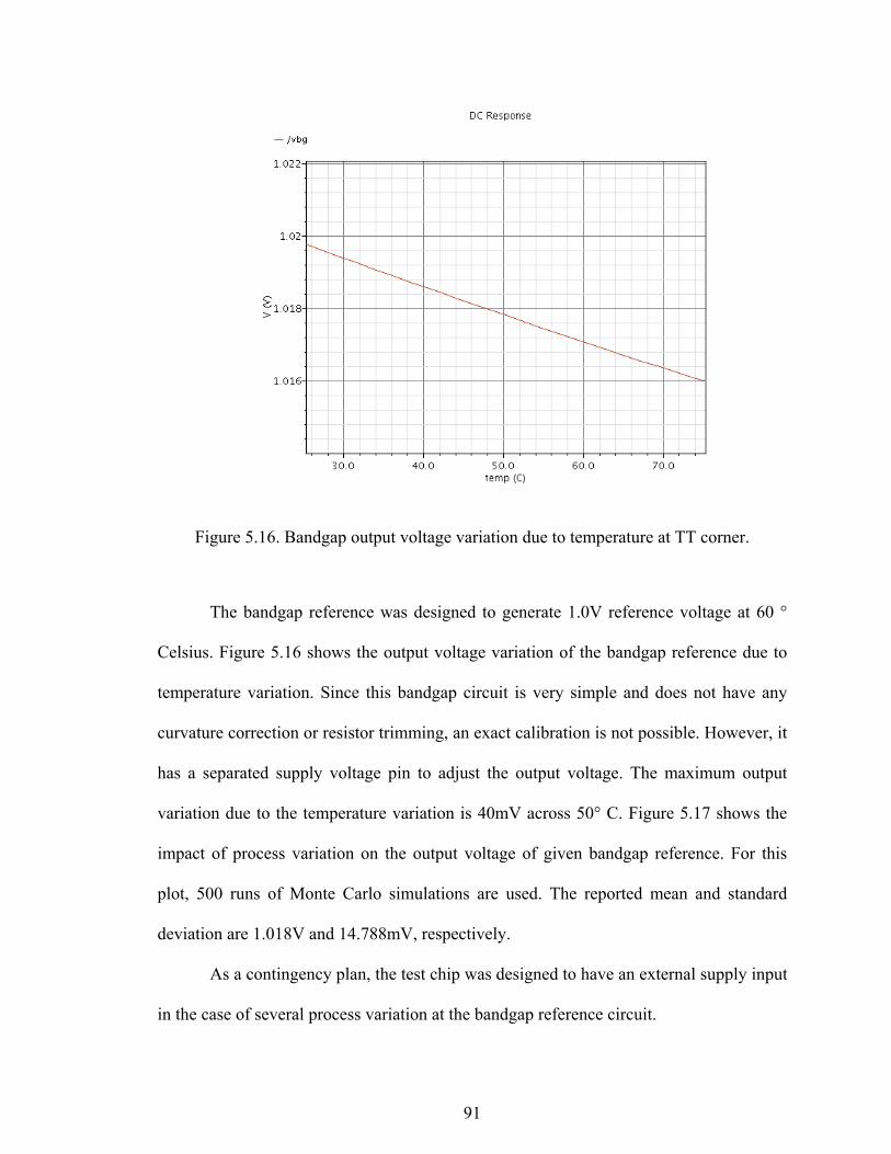
91
Figure 5.16. Bandgap output voltage variation due to temperature at TT corner.
The bandgap reference was designed to generate 1.0V reference voltage at 60 °
Celsius. Figure 5.16 shows the output voltage variation of the bandgap reference due to
temperature variation. Since this bandgap circuit is very simple and does not have any
curvature correction or resistor trimming, an exact calibration is not possible. However, it
has a separated supply voltage pin to adjust the output voltage. The maximum output
variation due to the temperature variation is 40mV across 50° C. Figure 5.17 shows the
impact of process variation on the output voltage of given bandgap reference. For this
plot, 500 runs of Monte Carlo simulations are used. The reported mean and standard
deviation are 1.018V and 14.788mV, respectively.
As a contingency plan, the test chip was designed to have an external supply input
in the case of several process variation at the bandgap reference circuit.
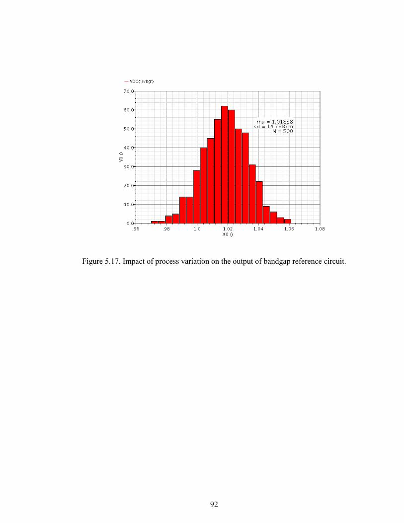
92
Figure 5.17. Impact of process variation on the output of bandgap reference circuit.
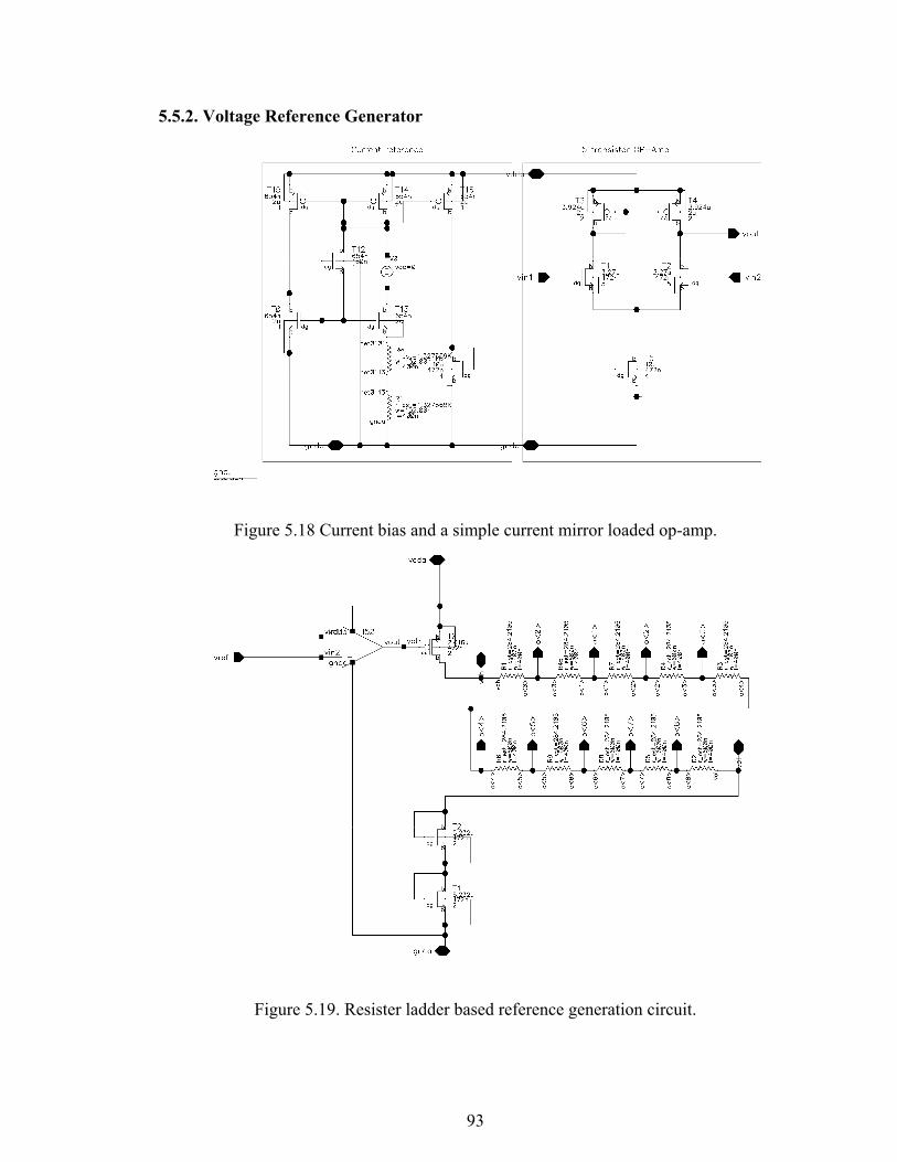
93
5.5.2. Voltage Reference Generator
Figure 5.18 Current bias and a simple current mirror loaded op-amp.
Figure 5.19. Resister ladder based reference generation circuit.
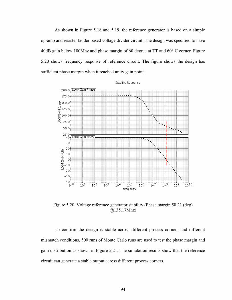
94
As shown in Figure 5.18 and 5.19, the reference generator is based on a simple
op-amp and resister ladder based voltage divider circuit. The design was specified to have
40dB gain below 100Mhz and phase margin of 60 degree at TT and 60° C corner. Figure
5.20 shows frequency response of reference circuit. The figure shows the design has
sufficient phase margin when it reached unity gain point.
Figure 5.20. Voltage reference generator stability (Phase margin 58.21 (deg) @135.17Mhz)
To confirm the design is stable across different process corners and different
mismatch conditions, 500 runs of Monte Carlo runs are used to test the phase margin and
gain distribution as shown in Figure 5.21. The simulation results show that the reference
circuit can generate a stable output across different process corners.
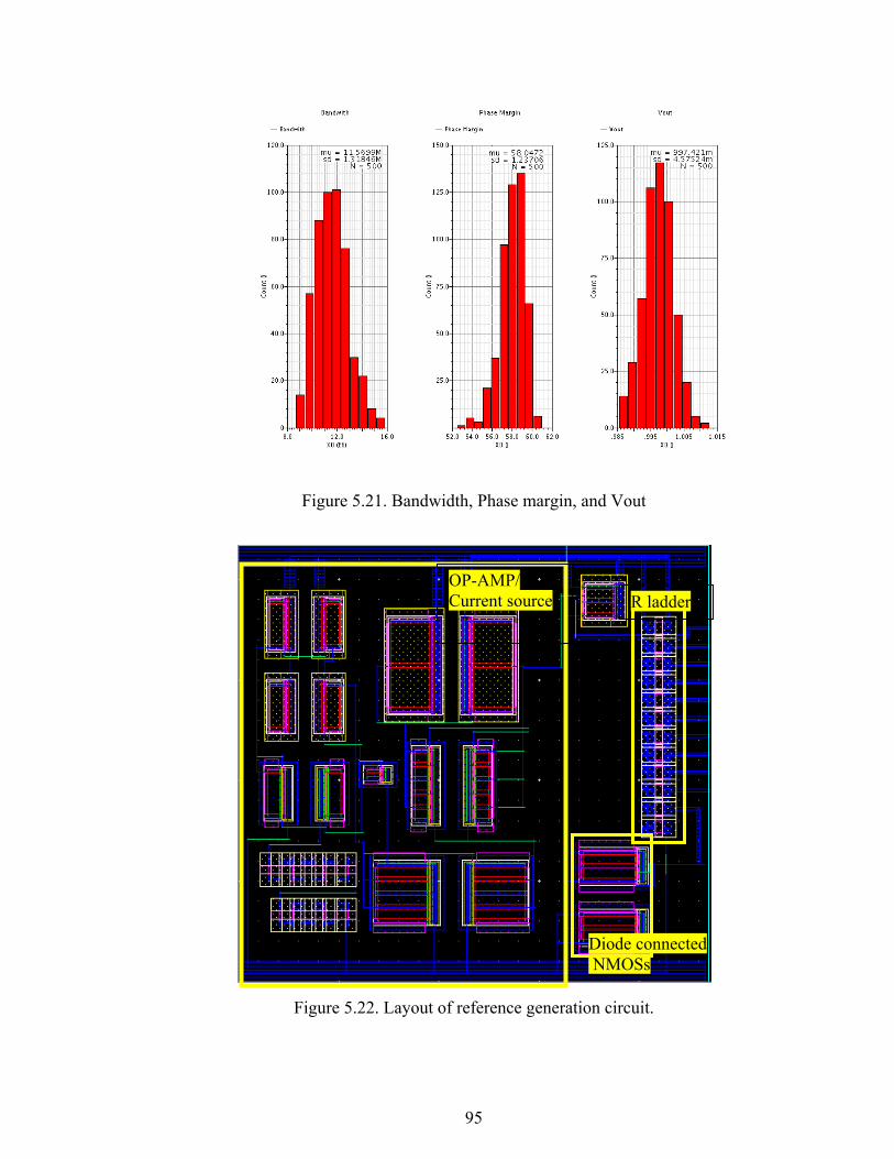
95
Figure 5.21. Bandwidth, Phase margin, and Vout
Figure 5.22. Layout of reference generation circuit.
OP-AMP/ Current source R ladder
Diode connected NMOSs
96
5.5.3 Voltage Controlled Ring Oscillator and Clock Distribution
The purpose of voltage controlled ring oscillator is to supply a reference clock to
all sub-blocks of the droop detector. To test the detector in different operation conditions,
the reference clock has to be adjustable. Also utilization of a stable digital supply voltage
for the clock distribution network is somewhat unfair; the distribution has to share the
noisy power supply with the droop detector system. To address these two requirements,
two different voltage domains were used. As shown in Figure 5.23, the ring oscillator
block was implemented with high voltage analog MOS devices. The clock distribution
was implemented low voltage digital MOS devices. To reduce the possibility of gate
breakdown when the voltage domain crossovers, the first stage of clock distribution was
implemented with high voltage analog MOS devices and those were powered by the
noisy digital power supply. Also, the ring oscillator has a gated input, this gating function
was not implemented for low power purposes, but it was added to achieve two objectives.
The first one is aiding convergence problem in full chip circuit simulation. The second
one is to help the analog block to reach a stable point in silicon implementation in a short
time.
Clock distribution was implemented in a binary clock distribution fashion. To
reduce the impact of skew, the clock distribution was recombined after each stage. As
shown in Figure 5.23 and 5.24, the total number of stages is 3 and this distribution covers
160um in y direction.
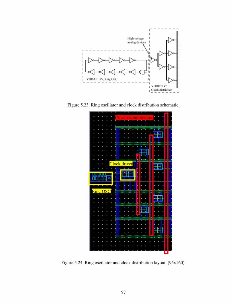
97
Figure 5.23. Ring oscillator and clock distribution schematic.
Figure 5.24. Ring oscillator and clock distribution layout. (95x160).
Ring OSC
Clock recombination
Clock driver
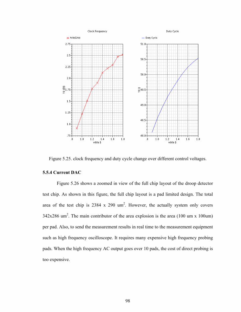
98
Figure 5.25. clock frequency and duty cycle change over different control voltages.
5.5.4 Current DAC
Figure 5.26 shows a zoomed in view of the full chip layout of the droop detector
test chip. As shown in this figure, the full chip layout is a pad limited design. The total
area of the test chip is 2384 x 290 um2. However, the actually system only covers
342x286 um2. The main contributor of the area explosion is the area (100 um x 100um)
per pad. Also, to send the measurement results in real time to the measurement equipment
such as high frequency oscilloscope. It requires many expensive high frequency probing
pads. When the high frequency AC output goes over 10 pads, the cost of direct probing is
too expensive.
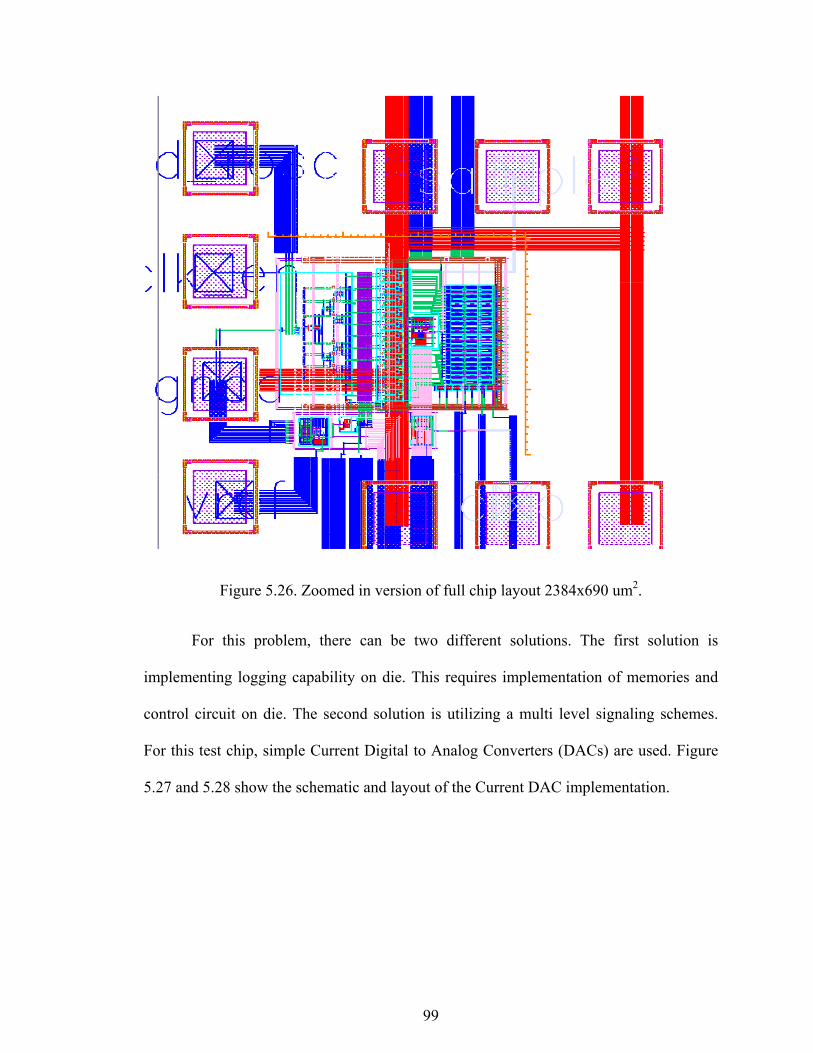
99
Figure 5.26. Zoomed in version of full chip layout 2384x690 um2.
For this problem, there can be two different solutions. The first solution is
implementing logging capability on die. This requires implementation of memories and
control circuit on die. The second solution is utilizing a multi level signaling schemes.
For this test chip, simple Current Digital to Analog Converters (DACs) are used. Figure
5.27 and 5.28 show the schematic and layout of the Current DAC implementation.
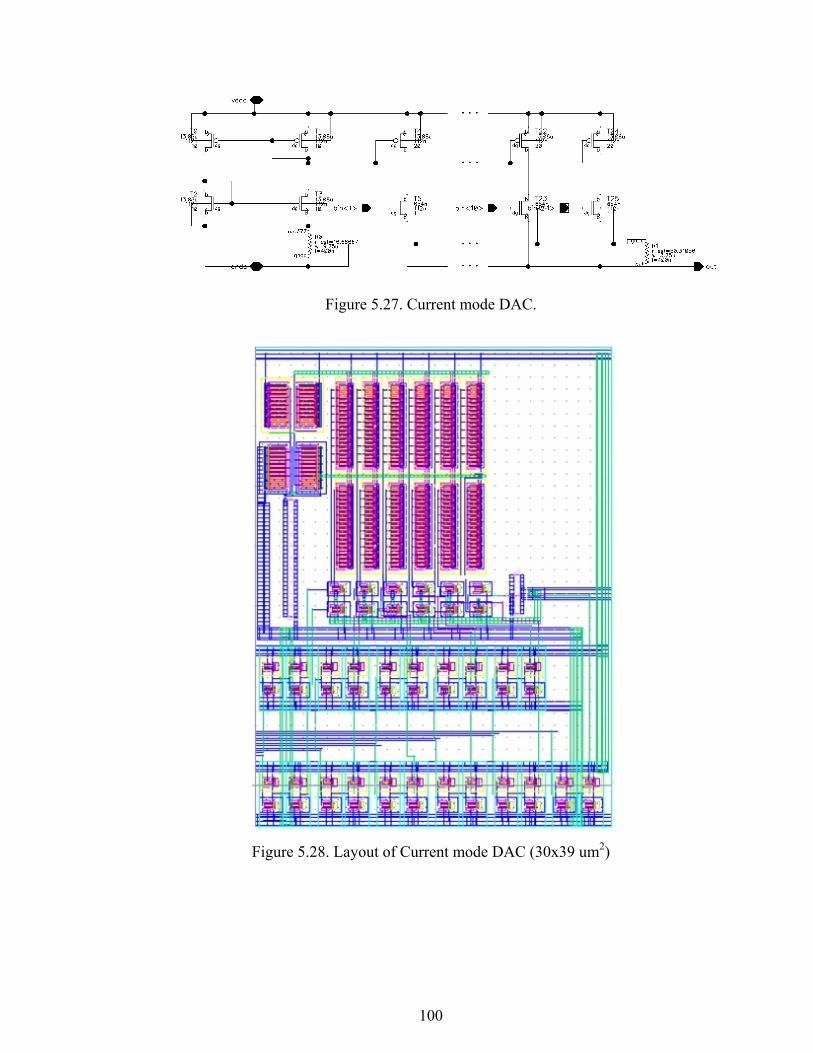
100
Figure 5.27. Current mode DAC.
Figure 5.28. Layout of Current mode DAC (30x39 um2)
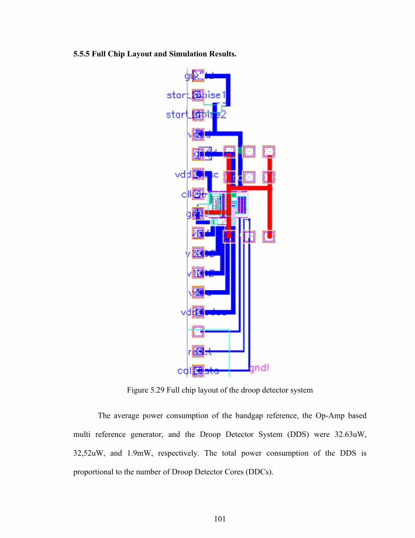
101
5.5.5 Full Chip Layout and Simulation Results.
Figure 5.29 Full chip layout of the droop detector system
The average power consumption of the bandgap reference, the Op-Amp based
multi reference generator, and the Droop Detector System (DDS) were 32.63uW,
32,52uW, and 1.9mW, respectively. The total power consumption of the DDS is
proportional to the number of Droop Detector Cores (DDCs).
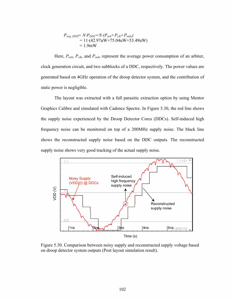
102
Pavg_DDS= N·PDDC=N·(Parb+Pclk+Psubs)
= 11·(42.97uW+75.04uW+53.49uW) = 1.9mW
Here, Parb, Pclk, and Psubs represent the average power consumption of an arbiter,
clock generation circuit, and two subblocks of a DDC, respectively. The power values are
generated based on 4GHz operation of the droop detector system, and the contribution of
static power is negligible.
The layout was extracted with a full parasitic extraction option by using Mentor
Graphics Calibre and simulated with Cadence Spectre. In Figure 5.30, the red line shows
the supply noise experienced by the Droop Detector Cores (DDCs). Self-induced high
frequency noise can be monitored on top of a 200MHz supply noise. The black line
shows the reconstructed supply noise based on the DDC outputs. The reconstructed
supply noise shows very good tracking of the actual supply noise.
Figure 5.30. Comparison between noisy supply and reconstructed supply voltage based on droop detector system outputs (Post layout simulation result).
103
5.6 Conclusion
In this work, an impedance profile of a realistic power supply network was built
upon openly accessible motherboard/VRM design specifications and the impedance
profile of Intel Nehalem microprocessor. Based on the findings regarding the required
specifications of a droop detector, a Droop Detector System (DDS) in IBM 45nm SOI
process is designed. Based on a careful design and detailed analysis, it is shown that the
DDS has the targeted design features: 1) 10-20mV resolution, 2) one clock cycle latency,
3) low power consumption, and 4) digital outputs. Moreover, the design is scalable in
terms of the detection range with the expense of linear area and power consumption.
Owing to the low latency digital output capability, this design can greatly improve an
adaptive clocking system with a digital control support. It can also assist architectural or
OS level decisions, when the logging capability is added to our DDS.
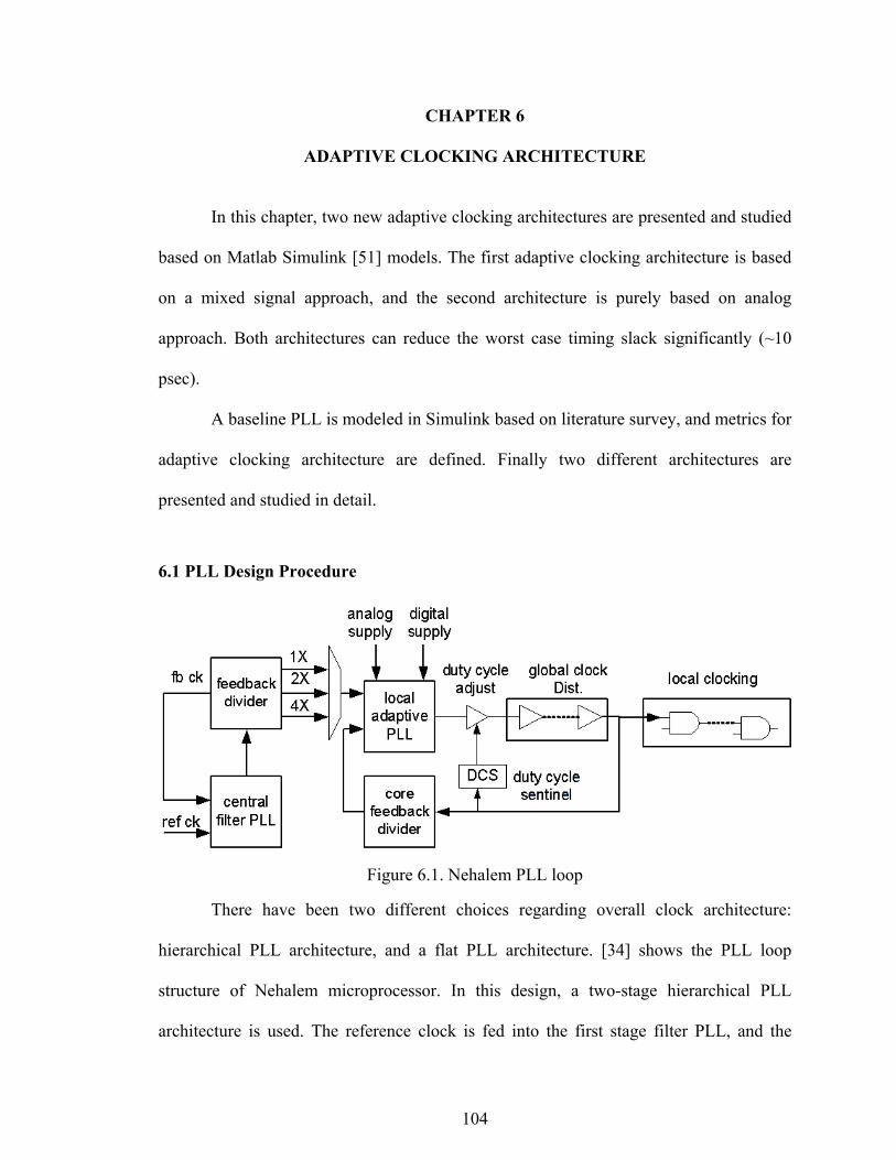
104
CHAPTER 6
ADAPTIVE CLOCKING ARCHITECTURE
In this chapter, two new adaptive clocking architectures are presented and studied
based on Matlab Simulink [51] models. The first adaptive clocking architecture is based
on a mixed signal approach, and the second architecture is purely based on analog
approach. Both architectures can reduce the worst case timing slack significantly (~10
psec).
A baseline PLL is modeled in Simulink based on literature survey, and metrics for
adaptive clocking architecture are defined. Finally two different architectures are
presented and studied in detail.
6.1 PLL Design Procedure
Figure 6.1. Nehalem PLL loop
There have been two different choices regarding overall clock architecture:
hierarchical PLL architecture, and a flat PLL architecture. [34] shows the PLL loop
structure of Nehalem microprocessor. In this design, a two-stage hierarchical PLL
architecture is used. The reference clock is fed into the first stage filter PLL, and the
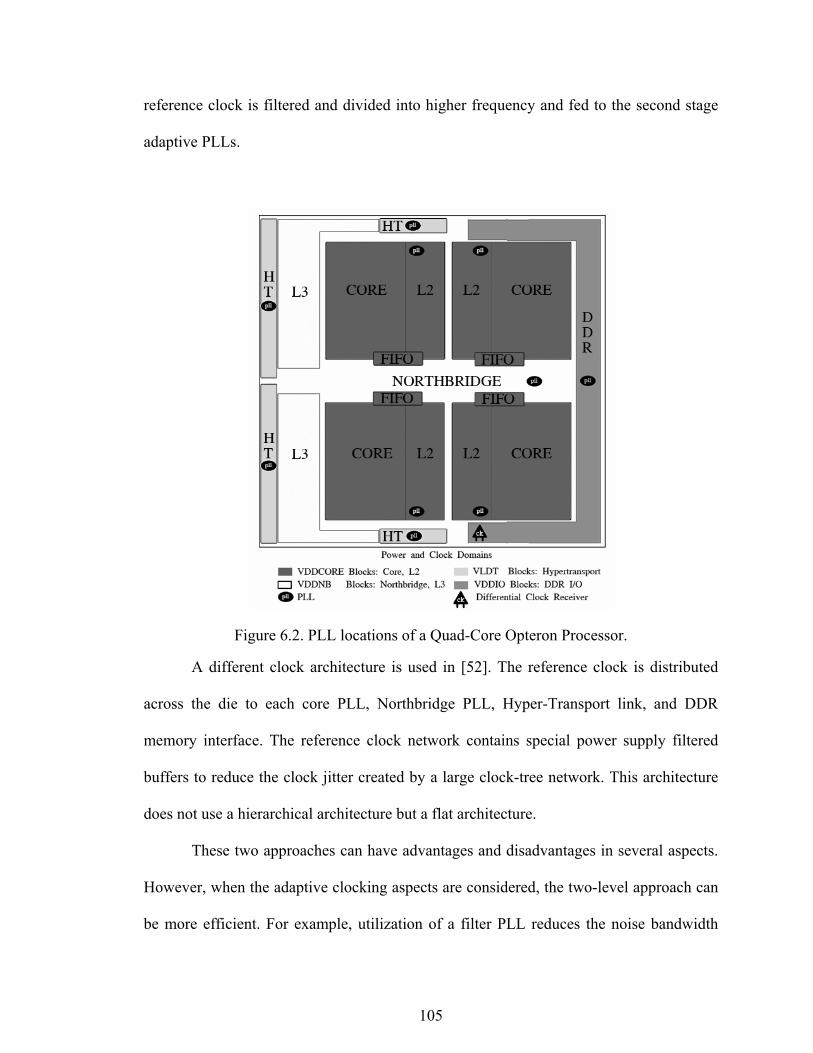
105
reference clock is filtered and divided into higher frequency and fed to the second stage
adaptive PLLs.
Figure 6.2. PLL locations of a Quad-Core Opteron Processor.
A different clock architecture is used in [52]. The reference clock is distributed
across the die to each core PLL, Northbridge PLL, Hyper-Transport link, and DDR
memory interface. The reference clock network contains special power supply filtered
buffers to reduce the clock jitter created by a large clock-tree network. This architecture
does not use a hierarchical architecture but a flat architecture.
These two approaches can have advantages and disadvantages in several aspects.
However, when the adaptive clocking aspects are considered, the two-level approach can
be more efficient. For example, utilization of a filter PLL reduces the noise bandwidth
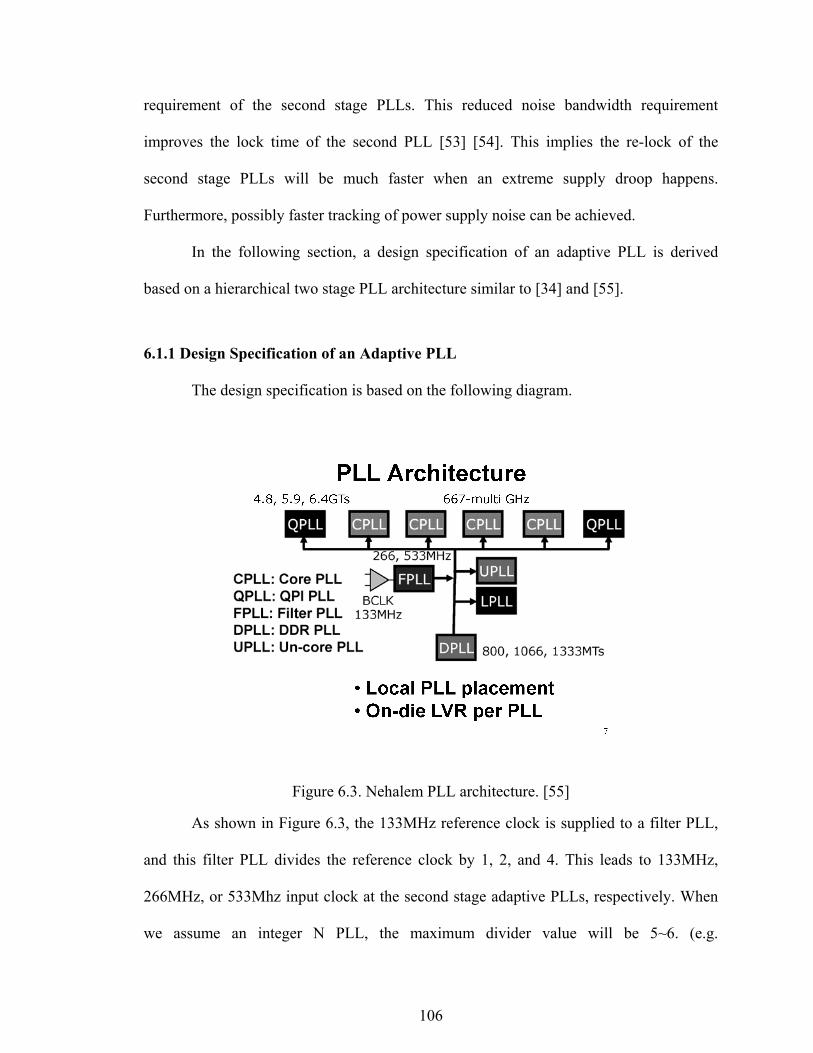
106
requirement of the second stage PLLs. This reduced noise bandwidth requirement
improves the lock time of the second PLL [53] [54]. This implies the re-lock of the
second stage PLLs will be much faster when an extreme supply droop happens.
Furthermore, possibly faster tracking of power supply noise can be achieved.
In the following section, a design specification of an adaptive PLL is derived
based on a hierarchical two stage PLL architecture similar to [34] and [55].
6.1.1 Design Specification of an Adaptive PLL
The design specification is based on the following diagram.
Figure 6.3. Nehalem PLL architecture. [55]
As shown in Figure 6.3, the 133MHz reference clock is supplied to a filter PLL,
and this filter PLL divides the reference clock by 1, 2, and 4. This leads to 133MHz,
266MHz, or 533Mhz input clock at the second stage adaptive PLLs, respectively. When
we assume an integer N PLL, the maximum divider value will be 5~6. (e.g.
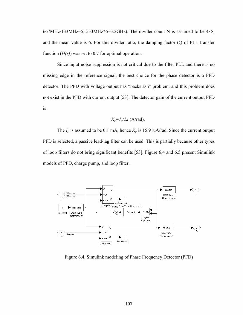
107
667MHz/133MHz=5, 533MHz*6=3.2GHz). The divider count N is assumed to be 4~8,
and the mean value is 6. For this divider ratio, the damping factor (ζ) of PLL transfer
function (H(s)) was set to 0.7 for optimal operation.
Since input noise suppression is not critical due to the filter PLL and there is no
missing edge in the reference signal, the best choice for the phase detector is a PFD
detector. The PFD with voltage output has “backslash” problem, and this problem does
not exist in the PFD with current output [53]. The detector gain of the current output PFD
is
Kp=Ip/2π (A/rad).
The Ip is assumed to be 0.1 mA, hence Kp is 15.91uA/rad. Since the current output
PFD is selected, a passive lead-lag filter can be used. This is partially because other types
of loop filters do not bring significant benefits [53]. Figure 6.4 and 6.5 present Simulink
models of PFD, charge pump, and loop filter.
Figure 6.4. Simulink modeling of Phase Frequency Detector (PFD)
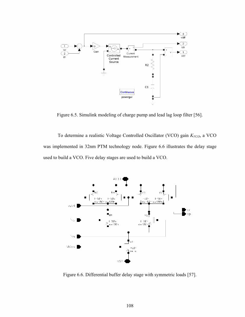
108
Figure 6.5. Simulink modeling of charge pump and lead lag loop filter [56].
To determine a realistic Voltage Controlled Oscillator (VCO) gain KVCO, a VCO
was implemented in 32nm PTM technology node. Figure 6.6 illustrates the delay stage
used to build a VCO. Five delay stages are used to build a VCO.
Figure 6.6. Differential buffer delay stage with symmetric loads [57].
109
KVCO is determined based on HSPCE simulations, and modeled as a Continuous-
Time VCO block in Simulink Communications BlockSet.
KVCO = (ωmax- ωmin)/(Vctr_max-Vctr_min)=5.15E10 Rad/V
To determine an appropriate value for the natural frequency ωn, we have to
consider two things. First, we have to consider the location of the tap-out point of the
feedback clock. We can tap out the VCO output and use it as a feedback clock, as shown
in many textbooks [14] [58], or we can tap-out the clock signal after the global clock
distribution, as shown in Figure 6.1. The first choice is better in terms of the stability of
the PLL. This is because the PLL usually has a separate power supply domain and the
clock distribution jitter is not applied back to the PLL. The second choice is better in
terms of dynamic adjustment of duty cycle, etc. However an adaptive PLL based on the
second choice can depart from the locked-in condition when severe supply noise causes a
large amount of period jitter in clock distribution. This severe period jitter can act as
frequency step, and it is desired that the PLL does not lock out when this happens.
Furthermore, it should recover to a locked-in state as soon as possible, when it is in the
out-of-lock condition. For this design requirement, the pull out range of ΔωPO must be
considered. ΔωPO defines the dynamic limit for stable operation of a PLL [53], and it is
required to be less than the reciprocal of the maximum cycle-to-cycle jitter.
ΔωPO=2π(1/(TCLK-C2CJ)-fCLK)=1.6E9
Finally, the natural frequency ωn can be calculated from the pull out range ΔωPO:
ωn= ΔωPO/(11.55(ζ+0.5)).
The filter capacitance C1 shown in Figure 6.5 can be calculated based on the following
formula.
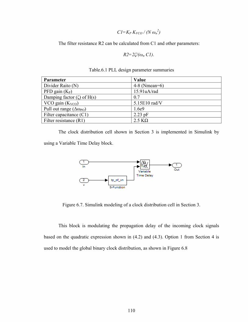
110
C1=KP KVCO / (N ωn2)
The filter resistance R2 can be calculated from C1 and other parameters:
R2=2ζ/(ωn C1).
Table.6.1 PLL design parameter summaries
Parameter Value Divider Raito (N) 4-8 (Nmean=6) PFD gain (KP) 15.91uA/rad Damping factor (ζ) of H(s) 0.7 VCO gain (KVCO) 5.15E10 rad/V Pull out range (ΔωPO) 1.6e9 Filter capacitance (C1) 2.23 pF Filter resistance (R1) 2.5 KΩ
The clock distribution cell shown in Section 3 is implemented in Simulink by
using a Variable Time Delay block.
Figure 6.7. Simulink modeling of a clock distribution cell in Section 3.
This block is modulating the propagation delay of the incoming clock signals
based on the quadratic expression shown in (4.2) and (4.3). Option 1 from Section 4 is
used to model the global binary clock distribution, as shown in Figure 6.8
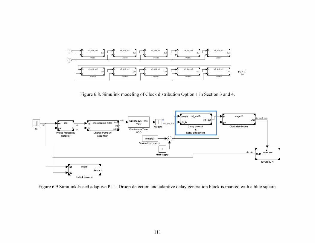
111
Figure 6.8. Simulink modeling of Clock distribution Option 1 in Section 3 and 4.
Figure 6.9 Simulink-based adaptive PLL. Droop detection and adaptive delay generation block is marked with a blue square.
1
Out
clk_dist_cellIn
vOut
Model9
clk_dist_cellIn
vOut
Model8
clk_dist_cellIn
vOut
Model7
clk_dist_cellIn
vOut
Model6
clk_dist_cellIn
vOut
Model5
clk_dist_cellIn
vOut
Model4
clk_dist_cellIn
vOut
Model3
clk_dist_cellIn
vOut
Model2
clk_dist_cellIn
vOut
Model1
clk_dist_cellIn
vOut
Model2
vn
1
In
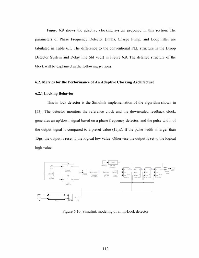
112
Figure 6.9 shows the adaptive clocking system proposed in this section. The
parameters of Phase Frequency Detector (PFD), Charge Pump, and Loop filter are
tabulated in Table 6.1. The difference to the conventional PLL structure is the Droop
Detector System and Delay line (dd_vcdl) in Figure 6.9. The detailed structure of the
block will be explained in the following sections.
6.2. Metrics for the Performance of An Adaptive Clocking Architecture
6.2.1 Locking Behavior
This in-lock detector is the Simulink implementation of the algorithm shown in
[53]. The detector monitors the reference clock and the downscaled feedback clock,
generates an up/down signal based on a phase frequency detector, and the pulse width of
the output signal is compared to a preset value (15ps). If the pulse width is larger than
15ps, the output is reset to the logical low value. Otherwise the output is set to the logical
high value.
Figure 6.10. Simulink modeling of an In-Lock detector
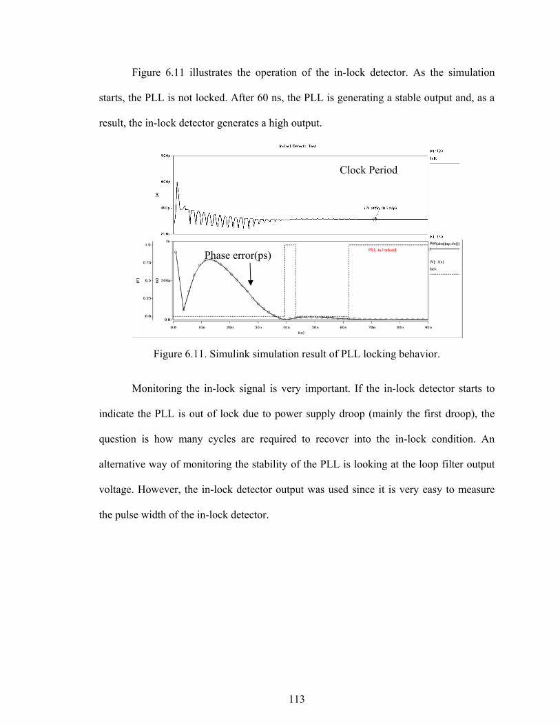
113
Figure 6.11 illustrates the operation of the in-lock detector. As the simulation
starts, the PLL is not locked. After 60 ns, the PLL is generating a stable output and, as a
result, the in-lock detector generates a high output.
Figure 6.11. Simulink simulation result of PLL locking behavior.
Monitoring the in-lock signal is very important. If the in-lock detector starts to
indicate the PLL is out of lock due to power supply droop (mainly the first droop), the
question is how many cycles are required to recover into the in-lock condition. An
alternative way of monitoring the stability of the PLL is looking at the loop filter output
voltage. However, the in-lock detector output was used since it is very easy to measure
the pulse width of the in-lock detector.
Clock Period ( )
Phase error(ps)
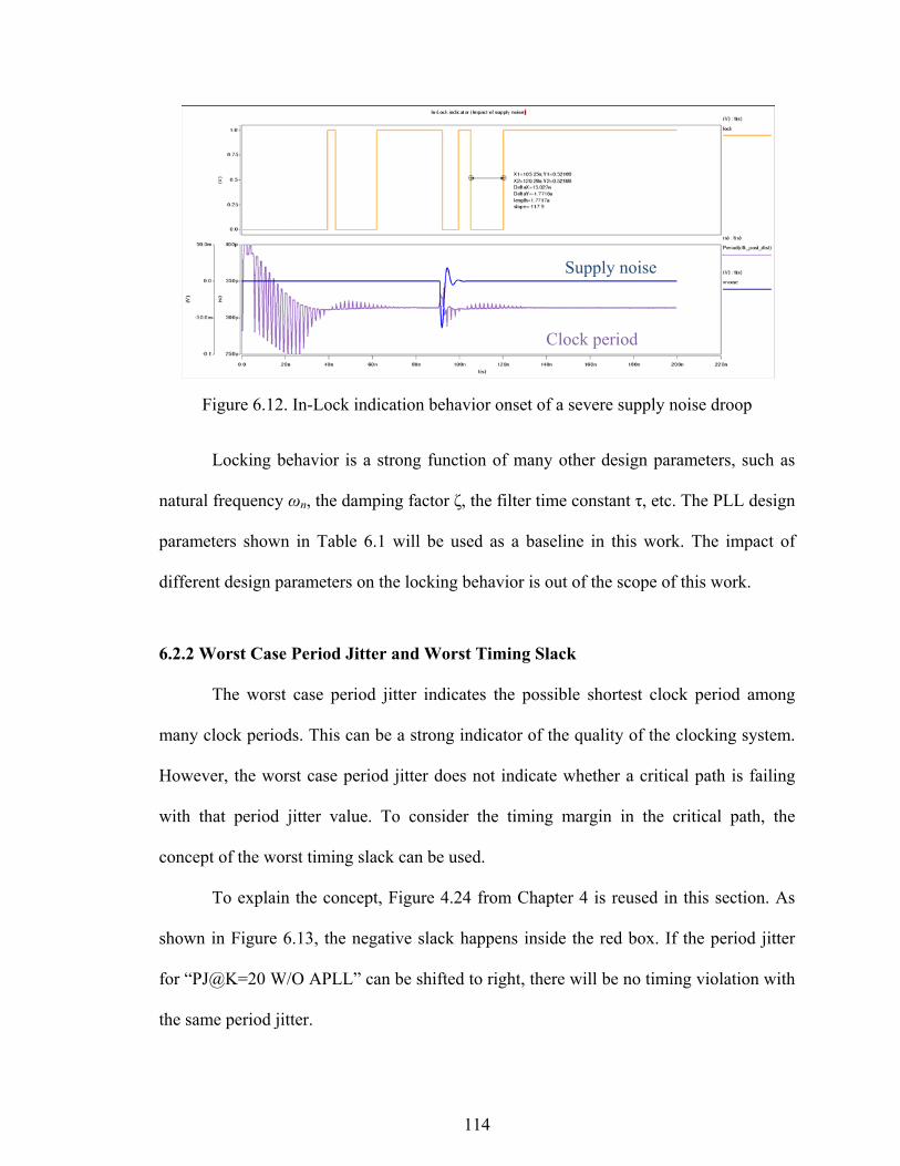
114
Figure 6.12. In-Lock indication behavior onset of a severe supply noise droop
Locking behavior is a strong function of many other design parameters, such as
natural frequency ωn, the damping factor ζ, the filter time constant τ, etc. The PLL design
parameters shown in Table 6.1 will be used as a baseline in this work. The impact of
different design parameters on the locking behavior is out of the scope of this work.
6.2.2 Worst Case Period Jitter and Worst Timing Slack
The worst case period jitter indicates the possible shortest clock period among
many clock periods. This can be a strong indicator of the quality of the clocking system.
However, the worst case period jitter does not indicate whether a critical path is failing
with that period jitter value. To consider the timing margin in the critical path, the
concept of the worst timing slack can be used.
To explain the concept, Figure 4.24 from Chapter 4 is reused in this section. As
shown in Figure 6.13, the negative slack happens inside the red box. If the period jitter
for “PJ@K=20 W/O APLL” can be shifted to right, there will be no timing violation with
the same period jitter.
Clock period
Supply noise
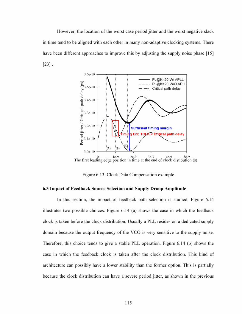
115
However, the location of the worst case period jitter and the worst negative slack
in time tend to be aligned with each other in many non-adaptive clocking systems. There
have been different approaches to improve this by adjusting the supply noise phase [15]
[23] .
Figure 6.13. Clock Data Compensation example
6.3 Impact of Feedback Source Selection and Supply Droop Amplitude
In this section, the impact of feedback path selection is studied. Figure 6.14
illustrates two possible choices. Figure 6.14 (a) shows the case in which the feedback
clock is taken before the clock distribution. Usually a PLL resides on a dedicated supply
domain because the output frequency of the VCO is very sensitive to the supply noise.
Therefore, this choice tends to give a stable PLL operation. Figure 6.14 (b) shows the
case in which the feedback clock is taken after the clock distribution. This kind of
architecture can possibly have a lower stability than the former option. This is partially
because the clock distribution can have a severe period jitter, as shown in the previous
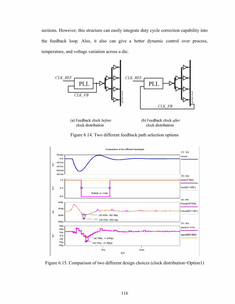
116
sections. However, this structure can easily integrate duty cycle correction capability into
the feedback loop. Also, it also can give a better dynamic control over process,
temperature, and voltage variation across a die.
Figure 6.14. Two different feedback path selection options
Figure 6.15. Comparison of two different design choices (clock distribution=Option1)
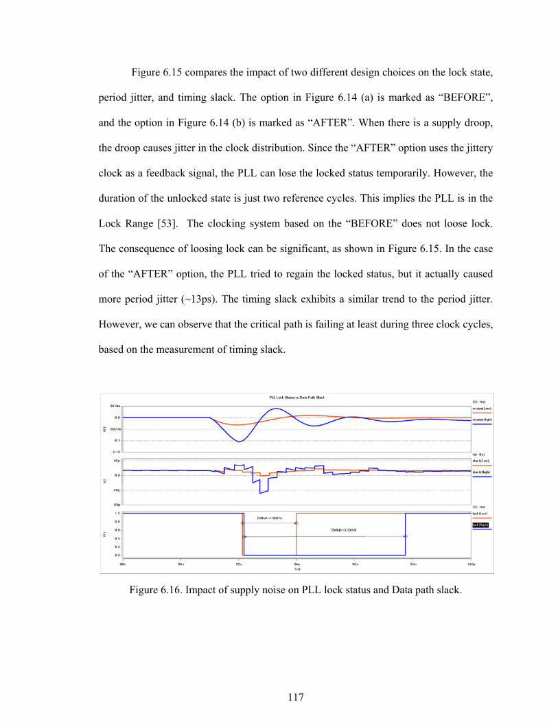
117
Figure 6.15 compares the impact of two different design choices on the lock state,
period jitter, and timing slack. The option in Figure 6.14 (a) is marked as “BEFORE”,
and the option in Figure 6.14 (b) is marked as “AFTER”. When there is a supply droop,
the droop causes jitter in the clock distribution. Since the “AFTER” option uses the jittery
clock as a feedback signal, the PLL can lose the locked status temporarily. However, the
duration of the unlocked state is just two reference cycles. This implies the PLL is in the
Lock Range [53]. The clocking system based on the “BEFORE” does not loose lock.
The consequence of loosing lock can be significant, as shown in Figure 6.15. In the case
of the “AFTER” option, the PLL tried to regain the locked status, but it actually caused
more period jitter (~13ps). The timing slack exhibits a similar trend to the period jitter.
However, we can observe that the critical path is failing at least during three clock cycles,
based on the measurement of timing slack.
Figure 6.16. Impact of supply noise on PLL lock status and Data path slack.
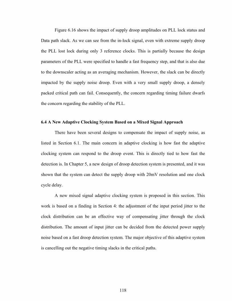
118
Figure 6.16 shows the impact of supply droop amplitudes on PLL lock status and
Data path slack. As we can see from the in-lock signal, even with extreme supply droop
the PLL lost lock during only 3 reference clocks. This is partially because the design
parameters of the PLL were specified to handle a fast frequency step, and that is also due
to the downscaler acting as an averaging mechanism. However, the slack can be directly
impacted by the supply noise droop. Even with a very small supply droop, a densely
packed critical path can fail. Consequently, the concern regarding timing failure dwarfs
the concern regarding the stability of the PLL.
6.4 A New Adaptive Clocking System Based on a Mixed Signal Approach
There have been several designs to compensate the impact of supply noise, as
listed in Section 6.1. The main concern in adaptive clocking is how fast the adaptive
clocking system can respond to the droop event. This is directly tied to how fast the
detection is. In Chapter 5, a new design of droop detection system is presented, and it was
shown that the system can detect the supply droop with 20mV resolution and one clock
cycle delay.
A new mixed signal adaptive clocking system is proposed in this section. This
work is based on a finding in Section 4: the adjustment of the input period jitter to the
clock distribution can be an effective way of compensating jitter through the clock
distribution. The amount of input jitter can be decided from the detected power supply
noise based on a fast droop detection system. The major objective of this adaptive system
is cancelling out the negative timing slacks in the critical paths.
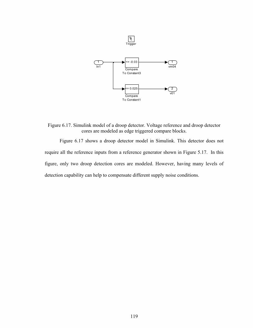
119
Figure 6.17. Simulink model of a droop detector. Voltage reference and droop detector cores are modeled as edge triggered compare blocks.
Figure 6.17 shows a droop detector model in Simulink. This detector does not
require all the reference inputs from a reference generator shown in Figure 5.17. In this
figure, only two droop detection cores are modeled. However, having many levels of
detection capability can help to compensate different supply noise conditions.
2
v01
1
vm04
<= -0.03
CompareTo Constant3
<= 0.025
CompareTo Constant1
Trigger
1
In1
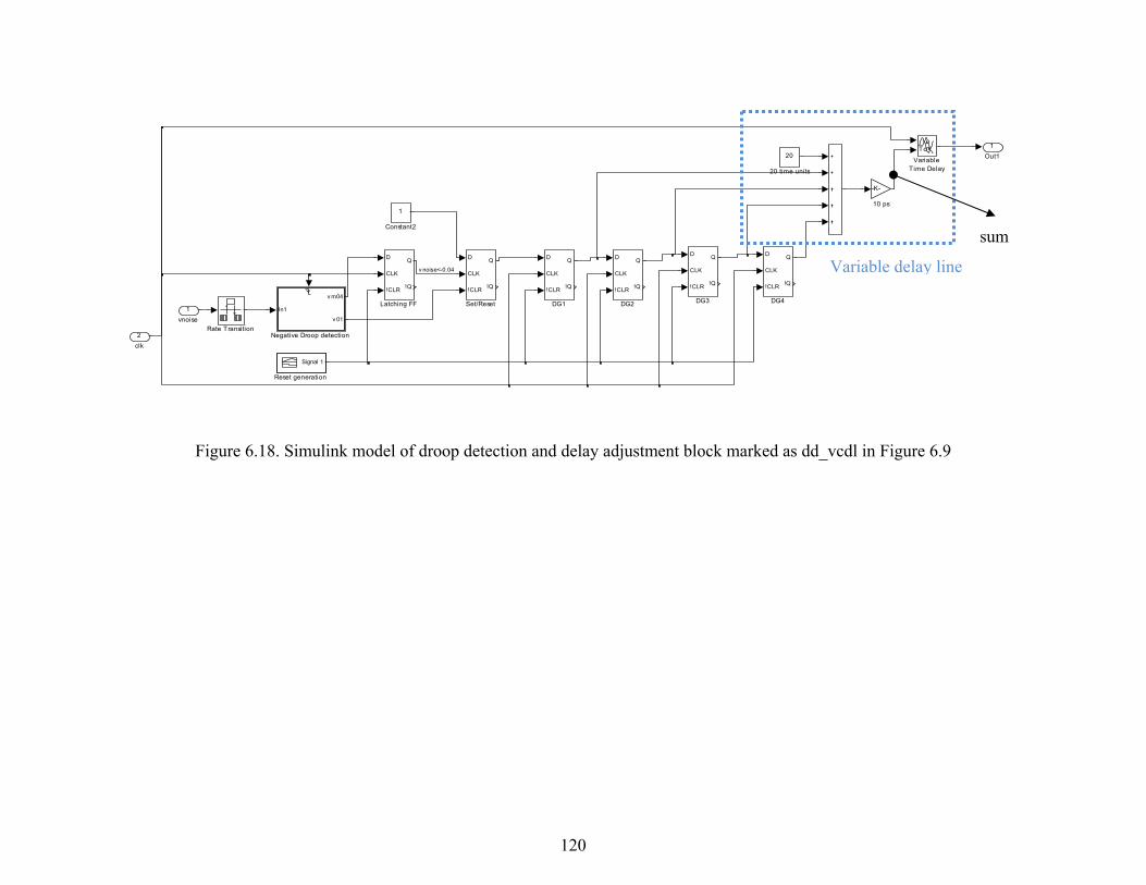
120
Figure 6.18. Simulink model of droop detection and delay adjustment block marked as dd_vcdl in Figure 6.9
1
Out1To
VariableTime Delay
D
CLK
!CLR
Q
!Q
Set/Reset
Signal 1
Reset generation
Rate Transition
In1
v m04
v 01
Negative Droop detection
D
CLK
!CLR
Q
!Q
Latching FF
D
CLK
!CLR
Q
!Q
DG4
D
CLK
!CLR
Q
!Q
DG3
D
CLK
!CLR
Q
!Q
DG2
D
CLK
!CLR
Q
!Q
DG1
1
Constant2
20
20 time units
-K-
10 ps
2
clk
1
vnoise
v noise<-0.04 Variable delay line
sum
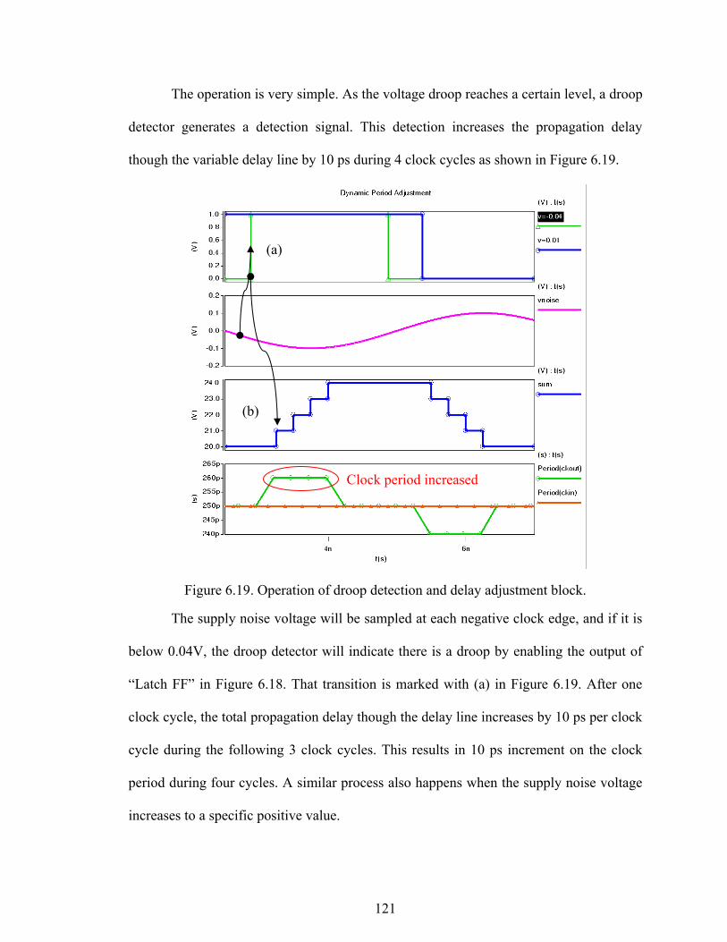
121
The operation is very simple. As the voltage droop reaches a certain level, a droop
detector generates a detection signal. This detection increases the propagation delay
though the variable delay line by 10 ps during 4 clock cycles as shown in Figure 6.19.
Figure 6.19. Operation of droop detection and delay adjustment block.
The supply noise voltage will be sampled at each negative clock edge, and if it is
below 0.04V, the droop detector will indicate there is a droop by enabling the output of
“Latch FF” in Figure 6.18. That transition is marked with (a) in Figure 6.19. After one
clock cycle, the total propagation delay though the delay line increases by 10 ps per clock
cycle during the following 3 clock cycles. This results in 10 ps increment on the clock
period during four cycles. A similar process also happens when the supply noise voltage
increases to a specific positive value.
(a)
(b)
Clock period increased
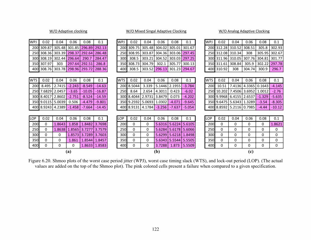
122
(a) (b) (c)
Figure 6.20. Shmoo plots of the worst case period jitter (WPJ), worst case timing slack (WTS), and lock-out period (LOP). (The actual values are added on the top of the Shmoo plot). The pink colored cells present a failure when compared to a given specification.
WPJ 0.02 0.04 0.06 0.08 0.1 WPJ 0.02 0.04 0.06 0.08 0.1 WPJ 0.02 0.04 0.06 0.08 0.1200 309.87 305.48 301.85 296.89 292.13 200 309.75 305.48 304.02 305.01 301.67 200 312.28 310.52 308.51 305.8 302.93250 308.36 303.39 298.37 292.64 286.48 250 308.95 303.87 304.36 303.06 297.45 250 312.08 310.34 308 305.95 302.67300 308.19 302.44 296.64 290.7 284.47 300 308.5 303.21 304.52 303.03 297.25 300 311.96 310.05 307.76 304.81 301.77350 307.97 303 297.64 292.51 286.8 350 308.73 304.79 302.1 305.77 300.13 350 311.61 308.84 305.9 302.22 297.78400 308.76 303.78 298.96 293.72 288.36 400 308.5 303.52 296.13 301.23 294.67 400 310.92 308 304.74 300.9 296.7
WTS 0.02 0.04 0.06 0.08 0.1 WTS 0.02 0.04 0.06 0.08 0.1 WTS 0.02 0.04 0.06 0.08 0.1200 8.495 2.7415 -2.243 -8.549 -14.63 200 8.5044 3.339 5.1446 2.1955 -3.784 200 10.51 7.4136 4.3365 0.1643 -4.145250 7.6829 2.0457 -3.65 -10.05 -16.87 250 8.64 2.654 4.3011 0.423 -6.02 250 10.202 7.4506 3.6952 1.0012 -2.76300 8.4017 2.8602 -2.751 -8.524 -14.59 300 8.4044 2.9731 3.8479 0.073 -4.202 300 9.9968 6.4155 2.6537 -1.329 -5.635350 9.0115 5.0039 0.506 -4.479 -9.801 350 9.2592 5.0693 1.0302 -4.071 -9.645 350 9.6475 5.6343 1.3289 -3.54 -8.305400 8.9243 4.2389 -1.458 -7.664 -14.45 400 8.9131 4.1784 -3.256 -7.637 -5.054 400 8.8592 5.2116 0.7985 -4.44 -10.12
LOP 0.02 0.04 0.06 0.08 0.1 LOP 0.02 0.04 0.06 0.08 0.1 LOP 0.02 0.04 0.06 0.08 0.1200 0 1.8643 1.858 1.8482 3.7698 200 0 0 5.6316 5.6224 5.6105 200 0 0 0 0 1.8621250 0 1.8638 1.8565 3.7277 3.7579 250 0 0 5.6284 5.6178 5.6066 250 0 0 0 0 0300 0 0 1.8573 3.7289 3.7603 300 0 0 5.6299 5.6218 1.8498 300 0 0 0 0 0350 0 0 1.861 1.8544 1.8457 350 0 0 5.6343 5.5544 5.5505 350 0 0 0 0 0400 0 0 0 1.8633 1.8583 400 0 0 3.7288 1.873 5.5509 400 0 0 0 0 0
W/O Adaptive clocking W/O Mixed Singal Adaptive Clocking W/O Analog Adaptive Clocking
123
Several Shmoo plots are shown in Figure 6.20. The first three plots on the left
side (column (a)) show the worst case period jitter (WPJ), worst case timing slack (WTS),
and lock-out period (LOP) for a clocking system without any adaptive clocking scheme.
These three plots serve as the references. The middle three plots (column (b)) are WPJ,
WTS, and LOP for the proposed mixed signal adaptive clocking architecture. The last
three plots on the right (column (c)) are WPJ, WTS, and LOP for an analog adaptive
clocking architecture presented in the following section. The pass/fail criteria for WPJ,
WTS, LOP are 300ps, 0s, and 0s, respectively.
The comparison between column (a) and (b) indicates the overall performance is
improved by utilizing dynamic delay adjustment. The WPJ, WTS, and LOP failing
corners were reduced to 28%, 57%, 93% of their original failure counts, respectively.
However, one interesting phenomenon can be found by observing the LOP of column (b).
Even though the failure count is lower than the original, the value of LOP at the failing
case is much higher than the LOP values in column (a). The reason behind this is the
adaptive clocking system is implemented as a mixed signal circuit. The supply voltage
level detection will always have quantization errors. Also, the delay line is adjusted by
digital control signals (discrete time domain signals), and this causes an abrupt jump in
the clock period. The combination of all these appear as a significantly longer lock out
period (LOP) compared to the original clocking system without any adaptive clocking
scheme.
However, we have to consider the fact that the selected architecture for this study
is the architecture that utilizes the distributed clock as a feedback signal, as shown in
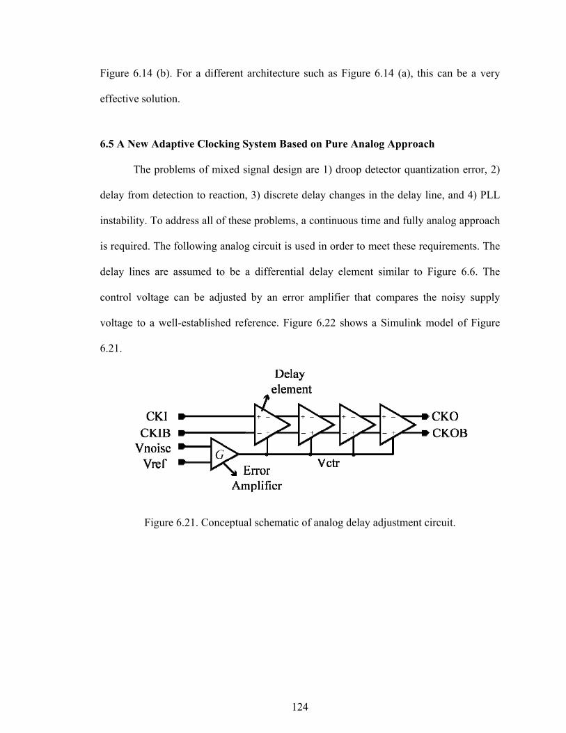
124
Figure 6.14 (b). For a different architecture such as Figure 6.14 (a), this can be a very
effective solution.
6.5 A New Adaptive Clocking System Based on Pure Analog Approach
The problems of mixed signal design are 1) droop detector quantization error, 2)
delay from detection to reaction, 3) discrete delay changes in the delay line, and 4) PLL
instability. To address all of these problems, a continuous time and fully analog approach
is required. The following analog circuit is used in order to meet these requirements. The
delay lines are assumed to be a differential delay element similar to Figure 6.6. The
control voltage can be adjusted by an error amplifier that compares the noisy supply
voltage to a well-established reference. Figure 6.22 shows a Simulink model of Figure
6.21.
Figure 6.21. Conceptual schematic of analog delay adjustment circuit.
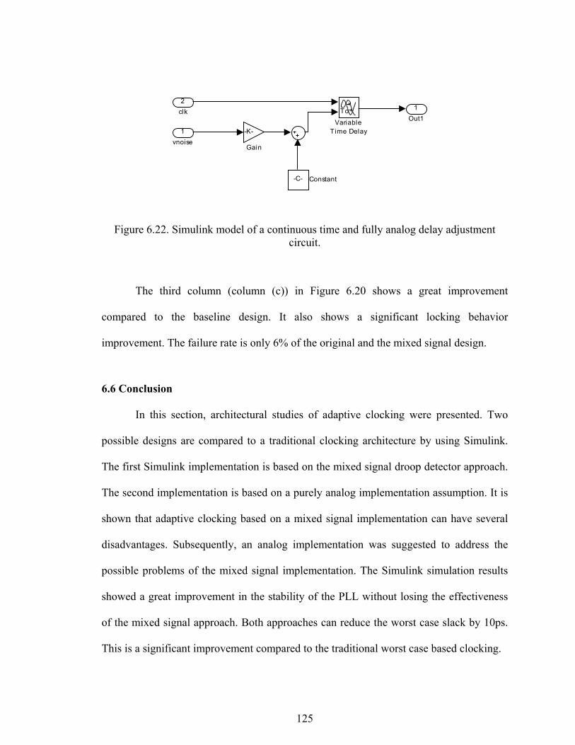
125
Figure 6.22. Simulink model of a continuous time and fully analog delay adjustment circuit.
The third column (column (c)) in Figure 6.20 shows a great improvement
compared to the baseline design. It also shows a significant locking behavior
improvement. The failure rate is only 6% of the original and the mixed signal design.
6.6 Conclusion
In this section, architectural studies of adaptive clocking were presented. Two
possible designs are compared to a traditional clocking architecture by using Simulink.
The first Simulink implementation is based on the mixed signal droop detector approach.
The second implementation is based on a purely analog implementation assumption. It is
shown that adaptive clocking based on a mixed signal implementation can have several
disadvantages. Subsequently, an analog implementation was suggested to address the
possible problems of the mixed signal implementation. The Simulink simulation results
showed a great improvement in the stability of the PLL without losing the effectiveness
of the mixed signal approach. Both approaches can reduce the worst case slack by 10ps.
This is a significant improvement compared to the traditional worst case based clocking.
1
Out1To
VariableTime Delay-K-
Gain
-C- Constant
2
clk
1
vnoise
126
CHAPTER 7
CONCLUSIONS AND FUTURE WORK
7.1 Conclusions
The dissertation concentrates on identifying and resolving major issues in clock
distribution and generation in high end microprocessors due to severe power supply noise.
The contribution of this dissertation crosses over three different boundaries: analytical
modeling, circuit design and implementation, and architectural studies, specifically
including these:
Analytical modeling of clock jitter in global clock distribution – Novel period
jitter expressions are formulated for global binary clock trees while considering the
details of different clock distribution parameters and time varying supply noise. Also, the
period jitter behavior in global binary clock tree is extensively analyzed with many
examples to provide an insight into period jitter induced by the first droop. Based on my
experiments, detailed guidelines for clock distribution design are suggested. The resulted
analytical expressions can predict the period jitter in the clock distribution with only 5 ps
error compared to HSPICE simulations.
Supply droop detection system design and implementation – a Droop Detector
System (DDS) in IBM 45nm SOI process is designed. Based on a careful design and
detailed analysis, it shows that the DDS has the targeted design features: 1) 10-20mV
resolution, 2) one clock cycle latency, 3) low power consumption, and 4) digital outputs.
Moreover, the design is scalable in terms of the detection range with the expense of linear
area and power consumption. Owing to the low latency digital output capability, this
design can greatly improve an adaptive clocking system with a digital control support.
127
Architectural study of adaptive clocking systems –Two possible adaptive
clocking systems are compared to a traditional clocking system based on Matlab
Simulink simulations. The results show that a mixed signal implementation can have
stability problems even though the worst case timing slack was effectively compensated.
Subsequently, an analog implementation was suggested to address the possible problems
of the mixed signal implementation. The simulation results present a great improvement
in the stability of the PLL without losing the effectiveness of the mixed signal approach.
Both approaches can reduce the worst case slack by 10ps. This is a significant
improvement compared to the traditional worst case based clocking.
7.2 Future work
3D IC integration based on Through Silicon Via (TSV) is now considered a
“must-have” technology for high end microprocessor, Graphics Processing Unit (GPU)
and Network-on-a-Chip (NoC). Clock generation and distribution architecture must
adjust to the new paradigm of 3D IC integration [59] [60]. Furthermore, the supply noise
and thermal problems [61] [62] in 3D IC can severely impact on the clock generation and
distribution architecture. I have been closely worked on 3D TSV based clocking [63], and
high speed signaling through TSVs [64]. As a straightforward extension of this work and
my previous work, many possible directions can be expected, including the following.
• High speed clock distribution though TSVs
• High speed clock distribution through interposer interconnect. [65]
• Impact of power supply impedance on clocking architecture.
• Supply droop detection and compensation in 3D ICs.
Exploration of forward clocking architecture [66] in 3D ICs.
128
APPENDIX A
MINIMUM REQUIRED ODER FOR APPROXIMATION
In Chapter 4, the propagation delay variation due to the power supply variation
was modeled as two quadratic expressions ((4.2) and (4.3)). In this appendix, the smallest
order for an approximated propagation delay equation is mathematically addressed.
If we assume a simple propagation delay expression
,
(A.1)
this can be simplified into
. (A.2)
(A.2) can be expanded to a Kth order Taylor series. At here, the objective is finding out
what is the smallest adequate order for an approximated polynomials. For simplicity, a
curve-fitted transistor parameters are used from [35], and the parameters are tabulated in
Table A.1.
Table A.1. Transistor parameters from [35]
Parameters value B 6.53336 x 10⁻⁵
n 1(~0.98572) λ 0.228148
Vth 0.34 W/L 105/70
From the Lagrange form of remainder of Taylor’s expression, if
(A.3)
on an interval (a-r, a+r) with some r>0, then
tp =0.5CLVDD
-VDD0.5 VDD W B
L VDD- Vthn 1+ lV „ V
tp =0.5CLL VDD - Vth-n
0.5 BW + 0.375 BVDDW l
fk+1 x £ M
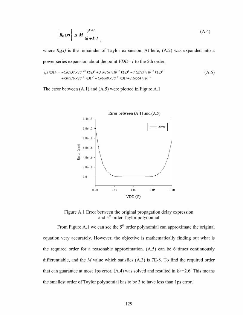
129
,
(A.4)
where Rk(x) is the remainder of Taylor expansion. At here, (A.2) was expanded into a
power series expansion about the point VDD=1 to the 5th order.
(A.5)
The error between (A.1) and (A.5) were plotted in Figure A.1
Figure A.1 Error between the original propagation delay expression and 5th order Taylor polynomial
From Figure A.1 we can see the 5th order polynomial can approximate the original
equation very accurately. However, the objective is mathematically finding out what is
the required order for a reasonable approximation. (A.5) can be 6 times continuously
differentiable, and the M value which satisfies (A.3) is 7E-8. To find the required order
that can guarantee at most 1ps error, (A.4) was solved and resulted in k>=2.6. This means
the smallest order of Taylor polynomial has to be 3 to have less than 1ps error.
Rk x £ M rk+1k+1 !
tp VDD = -5.83337μ 10-10 VDD5 + 3.30168μ 10-9 VDD4 - 7.62745μ 10-9 VDD3
+9.07316μ 10-9 VDD2 - 5.66369μ 10-9 VDD+ 1.56564μ 10-9
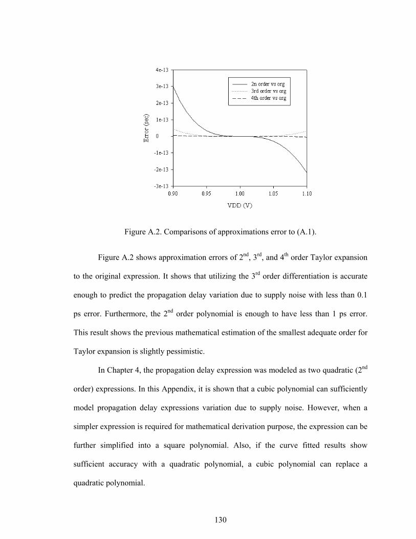
130
Figure A.2. Comparisons of approximations error to (A.1).
Figure A.2 shows approximation errors of 2nd, 3rd, and 4th order Taylor expansion
to the original expression. It shows that utilizing the 3rd order differentiation is accurate
enough to predict the propagation delay variation due to supply noise with less than 0.1
ps error. Furthermore, the 2nd order polynomial is enough to have less than 1 ps error.
This result shows the previous mathematical estimation of the smallest adequate order for
Taylor expansion is slightly pessimistic.
In Chapter 4, the propagation delay expression was modeled as two quadratic (2nd
order) expressions. In this Appendix, it is shown that a cubic polynomial can sufficiently
model propagation delay expressions variation due to supply noise. However, when a
simpler expression is required for mathematical derivation purpose, the expression can be
further simplified into a square polynomial. Also, if the curve fitted results show
sufficient accuracy with a quadratic polynomial, a cubic polynomial can replace a
quadratic polynomial.
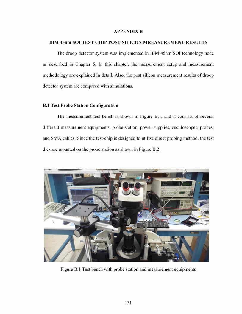
131
APPENDIX B
IBM 45nm SOI TEST CHIP POST SILICON MREASUREMENT RESULTS
The droop detector system was implemented in IBM 45nm SOI technology node
as described in Chapter 5. In this chapter, the measurement setup and measurement
methodology are explained in detail. Also, the post silicon measurement results of droop
detector system are compared with simulations.
B.1 Test Probe Station Configuration
The measurement test bench is shown in Figure B.1, and it consists of several
different measurement equipments: probe station, power supplies, oscilloscopes, probes,
and SMA cables. Since the test-chip is designed to utilize direct probing method, the test
dies are mounted on the probe station as shown in Figure B.2.
Figure B.1 Test bench with probe station and measurement equipments
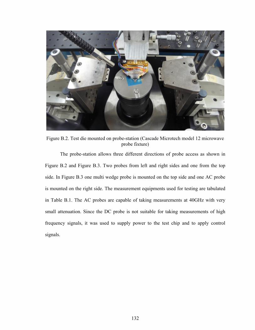
132
Figure B.2. Test die mounted on probe-station (Cascade Microtech model 12 microwave probe fixture)
The probe-station allows three different directions of probe access as shown in
Figure B.2 and Figure B.3. Two probes from left and right sides and one from the top
side. In Figure B.3 one multi wedge probe is mounted on the top side and one AC probe
is mounted on the right side. The measurement equipments used for testing are tabulated
in Table B.1. The AC probes are capable of taking measurements at 40GHz with very
small attenuation. Since the DC probe is not suitable for taking measurements of high
frequency signals, it was used to supply power to the test chip and to apply control
signals.
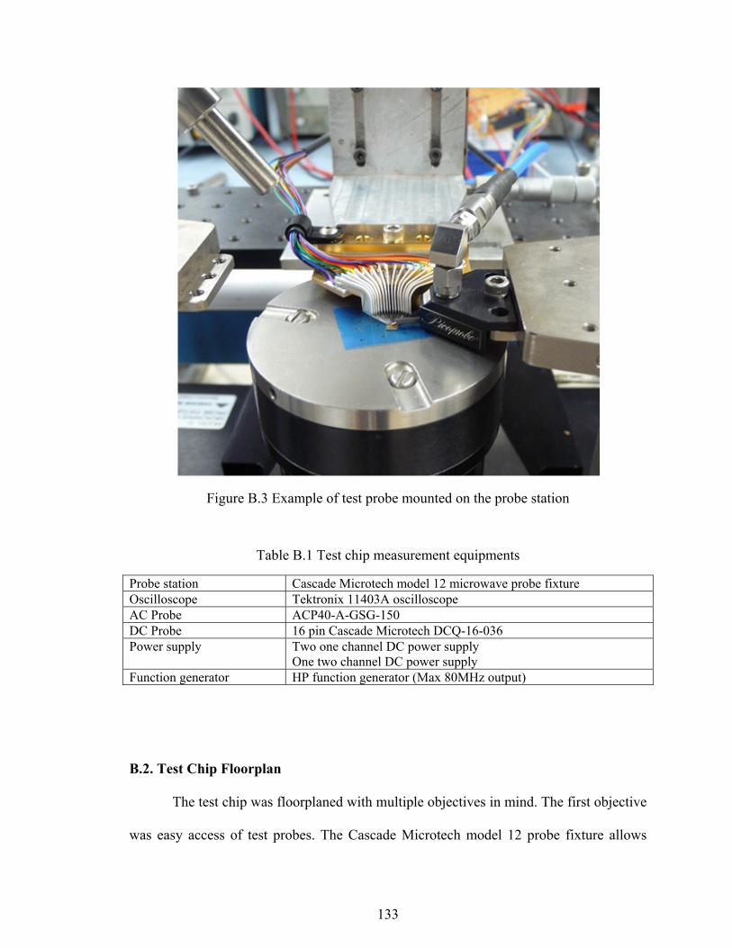
133
Figure B.3 Example of test probe mounted on the probe station
Table B.1 Test chip measurement equipments
Probe station Cascade Microtech model 12 microwave probe fixture Oscilloscope Tektronix 11403A oscilloscope AC Probe ACP40-A-GSG-150 DC Probe 16 pin Cascade Microtech DCQ-16-036 Power supply Two one channel DC power supply
One two channel DC power supply Function generator HP function generator (Max 80MHz output)
B.2. Test Chip Floorplan
The test chip was floorplaned with multiple objectives in mind. The first objective
was easy access of test probes. The Cascade Microtech model 12 probe fixture allows
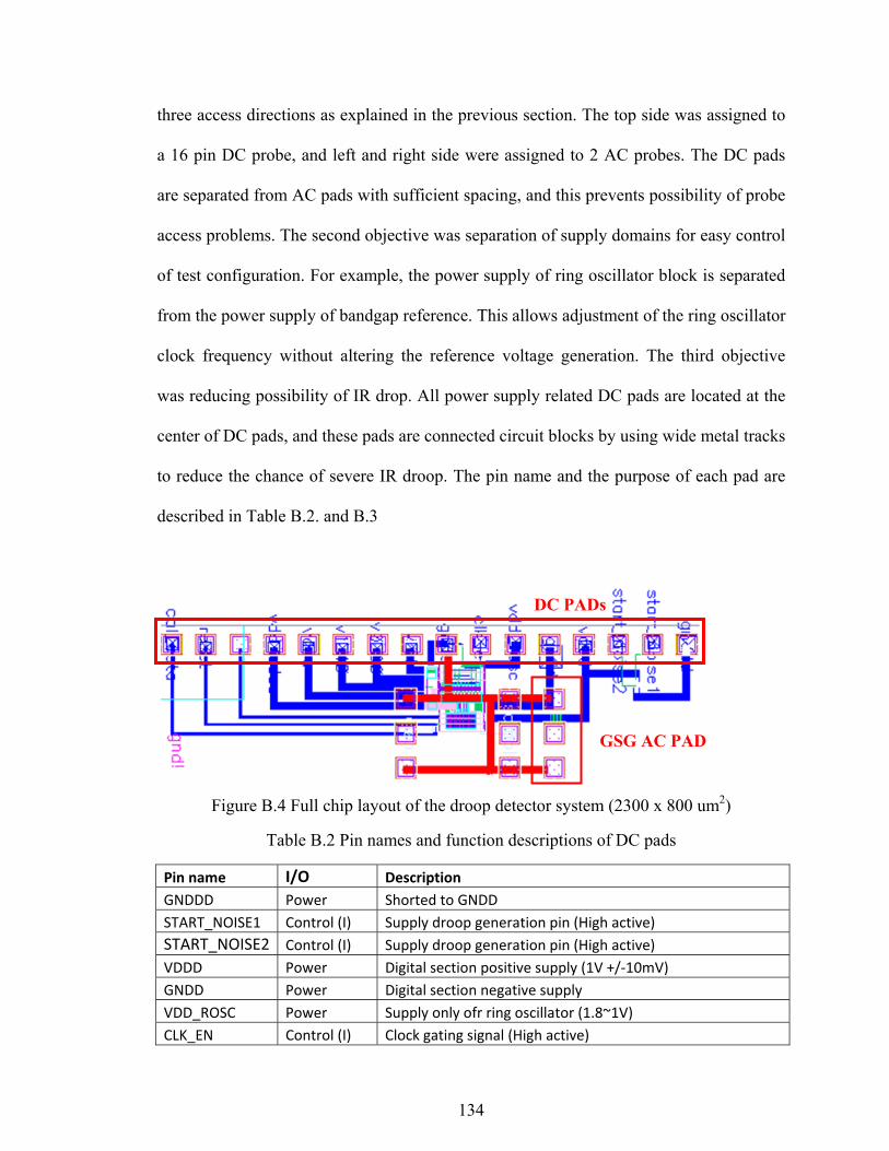
134
three access directions as explained in the previous section. The top side was assigned to
a 16 pin DC probe, and left and right side were assigned to 2 AC probes. The DC pads
are separated from AC pads with sufficient spacing, and this prevents possibility of probe
access problems. The second objective was separation of supply domains for easy control
of test configuration. For example, the power supply of ring oscillator block is separated
from the power supply of bandgap reference. This allows adjustment of the ring oscillator
clock frequency without altering the reference voltage generation. The third objective
was reducing possibility of IR drop. All power supply related DC pads are located at the
center of DC pads, and these pads are connected circuit blocks by using wide metal tracks
to reduce the chance of severe IR droop. The pin name and the purpose of each pad are
described in Table B.2. and B.3
Figure B.4 Full chip layout of the droop detector system (2300 x 800 um2)
Table B.2 Pin names and function descriptions of DC pads
Pin name I/O DescriptionGNDDD Power Shorted to GNDDSTART_NOISE1 Control (I) Supply droop generation pin (High active) START_NOISE2 Control (I) Supply droop generation pin (High active) VDDD Power Digital section positive supply (1V +/-10mV) GNDD Power Digital section negative supplyVDD_ROSC Power Supply only ofr ring oscillator (1.8~1V) CLK_EN Control (I) Clock gating signal (High active)
DC PADs
GSG AC PAD
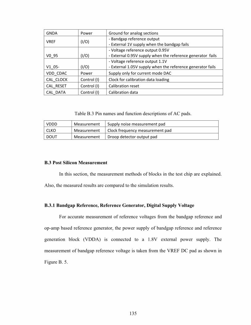
135
GNDA Power Ground for analog sections
VREF (I/O) - Bandgap reference output- External 1V supply when the bandgap fails
V0_95 (I/O) - Voltage reference output 0.95V- External 0.95V supply when the reference generator fails
V1_05- (I/O) - Voltage reference output 1.1V- External 1.05V supply when the reference generator fails
VDD_CDAC Power Supply only for current mode DACCAL_CLOCK Control (I) Clock for calibration data loadingCAL_RESET Control (I) Calibration resetCAL_DATA Control (I) Calibration data
Table B.3 Pin names and function descriptions of AC pads.
VDDD Measurement Supply noise measurement padCLKO Measurement Clock frequency measurement padDOUT Measurement Droop detector output pad
B.3 Post Silicon Measurement
In this section, the measurement methods of blocks in the test chip are explained.
Also, the measured results are compared to the simulation results.
B.3.1 Bandgap Reference, Reference Generator, Digital Supply Voltage
For accurate measurement of reference voltages from the bandgap reference and
op-amp based reference generator, the power supply of bandgap reference and reference
generation block (VDDA) is connected to a 1.8V external power supply. The
measurement of bandgap reference voltage is taken from the VREF DC pad as shown in
Figure B. 5.
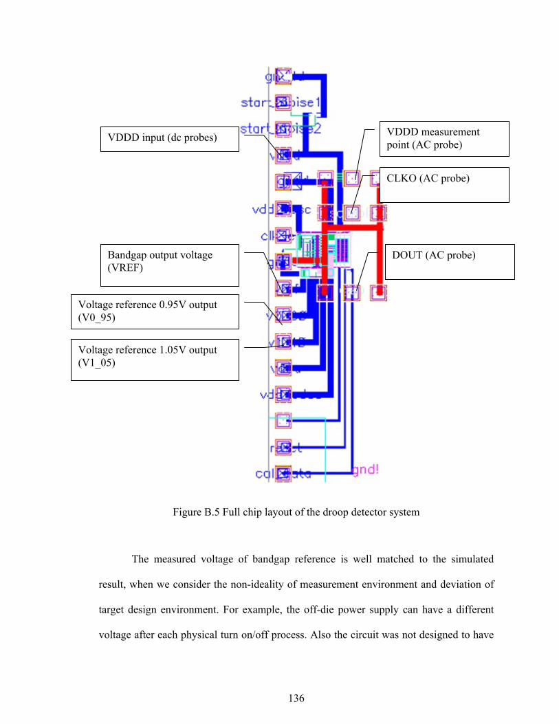
136
Figure B.5 Full chip layout of the droop detector system
The measured voltage of bandgap reference is well matched to the simulated
result, when we consider the non-ideality of measurement environment and deviation of
target design environment. For example, the off-die power supply can have a different
voltage after each physical turn on/off process. Also the circuit was not designed to have
VDDD measurement point (AC probe)
VDDD input (dc probes)
Bandgap output voltage (VREF)
Voltage reference 0.95V output (V0_95)
Voltage reference 1.05V output (V1_05)
CLKO (AC probe)
DOUT (AC probe)
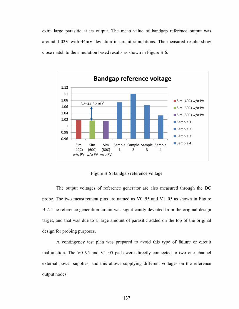
137
extra large parasitic at its output. The mean value of bandgap reference output was
around 1.02V with 44mV deviation in circuit simulations. The measured results show
close match to the simulation based results as shown in Figure B.6.
Figure B.6 Bandgap reference voltage
The output voltages of reference generator are also measured through the DC
probe. The two measurement pins are named as V0_95 and V1_05 as shown in Figure
B.7. The reference generation circuit was significantly deviated from the original design
target, and that was due to a large amount of parasitic added on the top of the original
design for probing purposes.
A contingency test plan was prepared to avoid this type of failure or circuit
malfunction. The V0_95 and V1_05 pads were directly connected to two one channel
external power supplies, and this allows supplying different voltages on the reference
output nodes.
0.96
0.98
1
1.02
1.04
1.06
1.08
1.1
1.12
Sim (40C)
w/o PV
Sim (60C)
w/o PV
Sim (80C)
w/o PV
Sample 1
Sample 2
Sample 3
Sample 4
Bandgap reference voltage
Sim (40C) w/o PV
Sim (60C) w/o PV
Sim (80C) w/o PV
Sample 1
Sample 2
Sample 3
Sample 4
3σ=44.36 mV
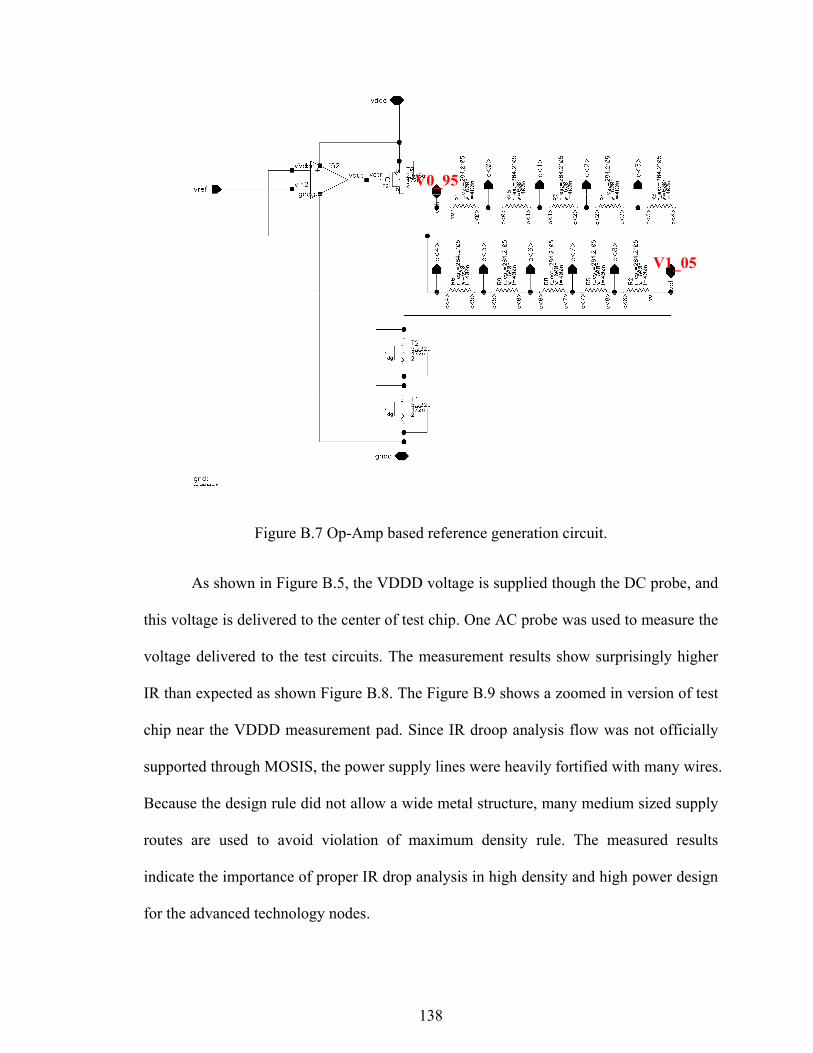
138
Figure B.7 Op-Amp based reference generation circuit.
As shown in Figure B.5, the VDDD voltage is supplied though the DC probe, and
this voltage is delivered to the center of test chip. One AC probe was used to measure the
voltage delivered to the test circuits. The measurement results show surprisingly higher
IR than expected as shown Figure B.8. The Figure B.9 shows a zoomed in version of test
chip near the VDDD measurement pad. Since IR droop analysis flow was not officially
supported through MOSIS, the power supply lines were heavily fortified with many wires.
Because the design rule did not allow a wide metal structure, many medium sized supply
routes are used to avoid violation of maximum density rule. The measured results
indicate the importance of proper IR drop analysis in high density and high power design
for the advanced technology nodes.
V0_95
V1_05
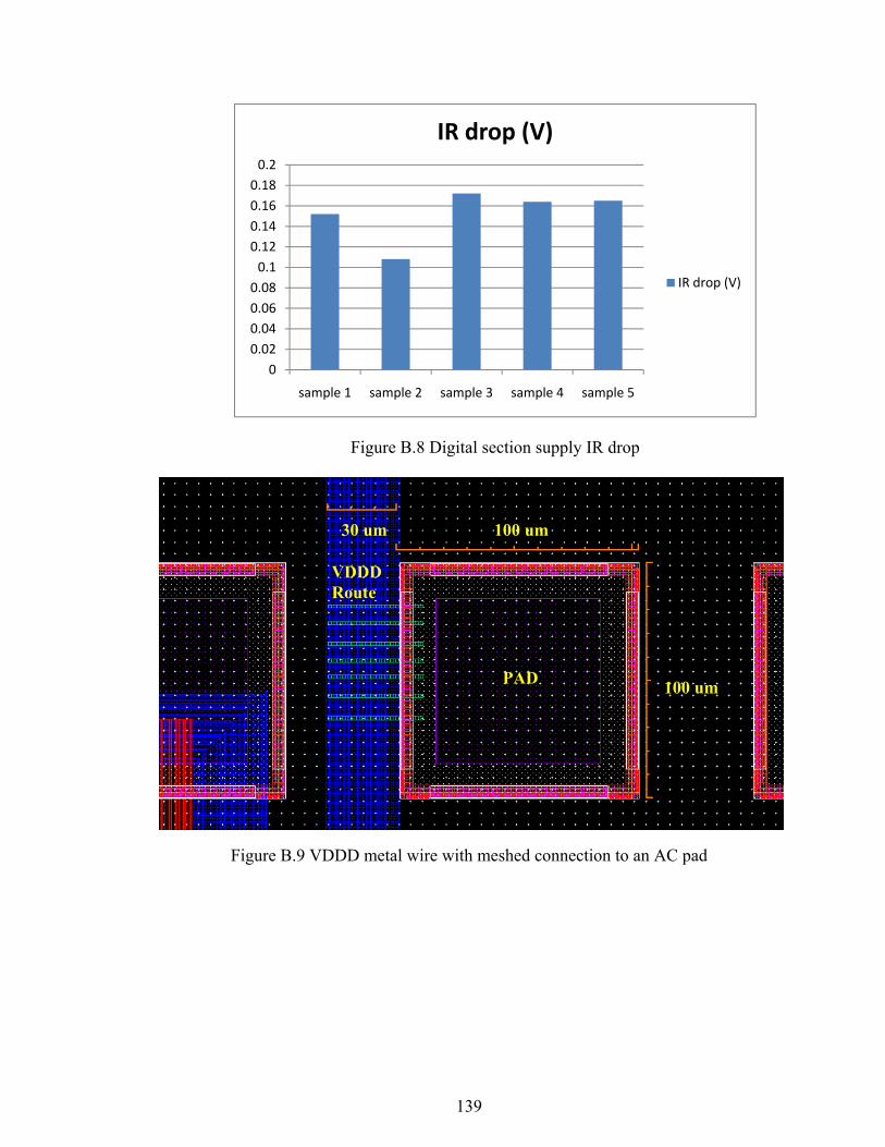
139
Figure B.8 Digital section supply IR drop
Figure B.9 VDDD metal wire with meshed connection to an AC pad
00.020.040.060.08
0.10.120.140.160.18
0.2
sample 1 sample 2 sample 3 sample 4 sample 5
IR drop (V)
IR drop (V)
30 um 100 um
100 um PAD
VDDD Route
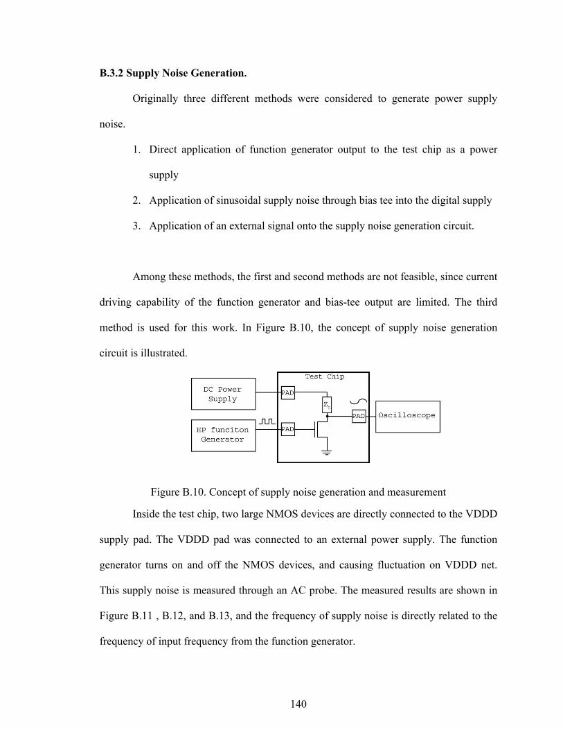
140
B.3.2 Supply Noise Generation.
Originally three different methods were considered to generate power supply
noise.
1. Direct application of function generator output to the test chip as a power
supply
2. Application of sinusoidal supply noise through bias tee into the digital supply
3. Application of an external signal onto the supply noise generation circuit.
Among these methods, the first and second methods are not feasible, since current
driving capability of the function generator and bias-tee output are limited. The third
method is used for this work. In Figure B.10, the concept of supply noise generation
circuit is illustrated.
Figure B.10. Concept of supply noise generation and measurement
Inside the test chip, two large NMOS devices are directly connected to the VDDD
supply pad. The VDDD pad was connected to an external power supply. The function
generator turns on and off the NMOS devices, and causing fluctuation on VDDD net.
This supply noise is measured through an AC probe. The measured results are shown in
Figure B.11 , B.12, and B.13, and the frequency of supply noise is directly related to the
frequency of input frequency from the function generator.
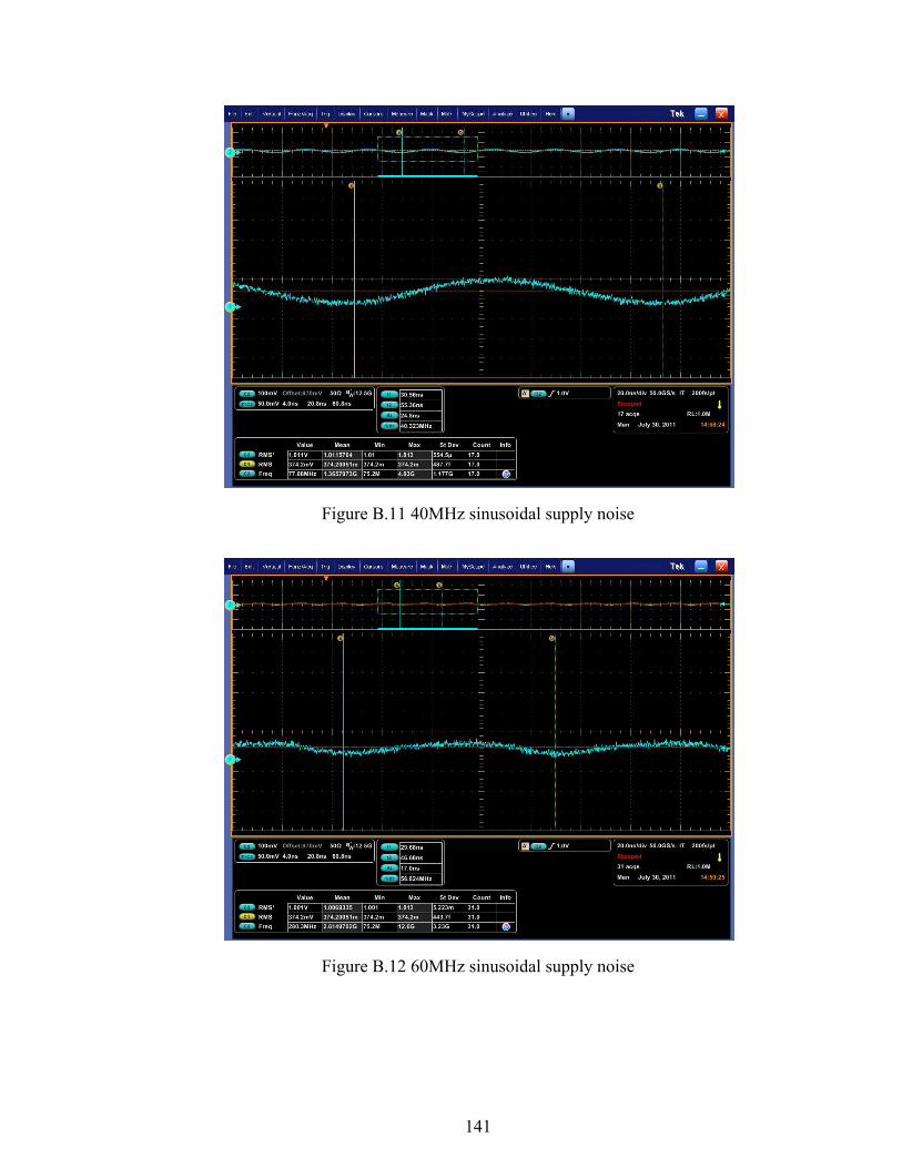
141
Figure B.11 40MHz sinusoidal supply noise
Figure B.12 60MHz sinusoidal supply noise
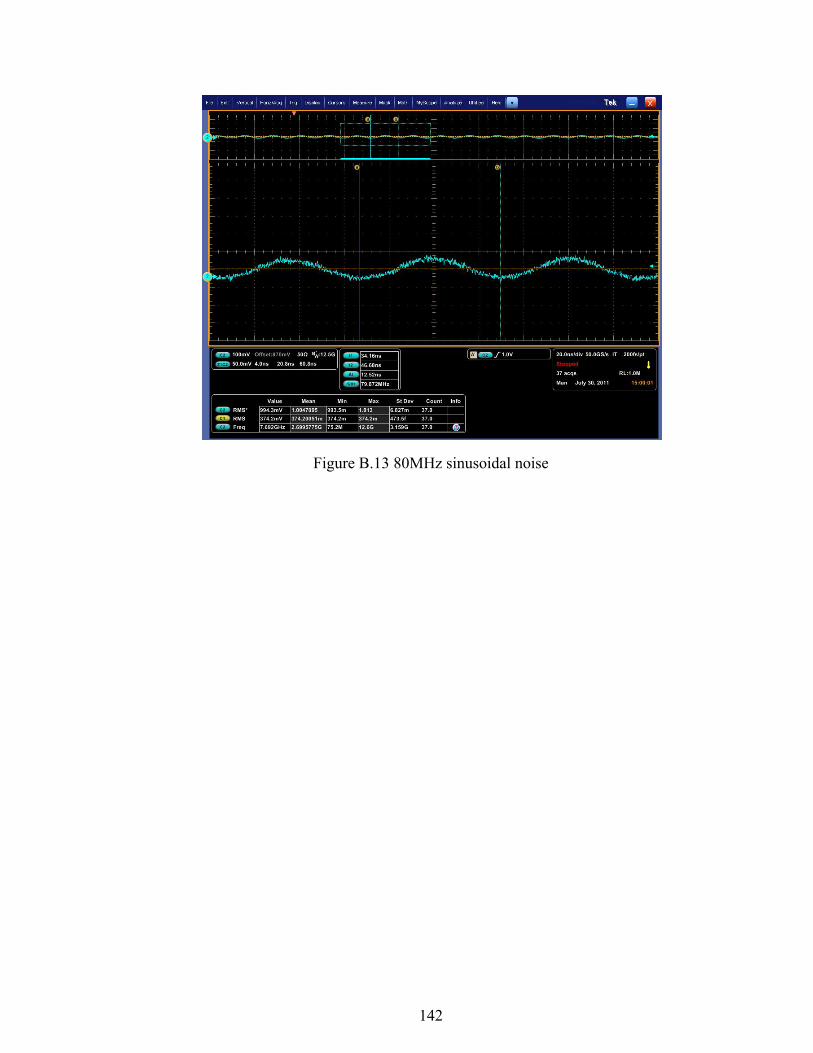
142
Figure B.13 80MHz sinusoidal noise
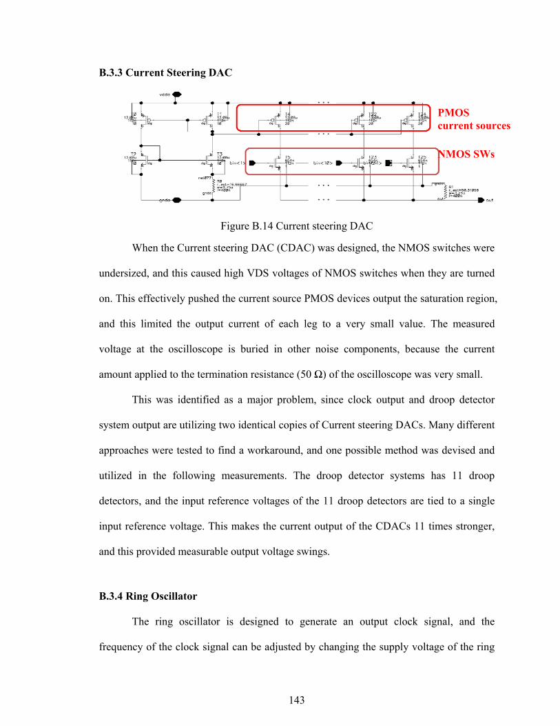
143
B.3.3 Current Steering DAC
Figure B.14 Current steering DAC
When the Current steering DAC (CDAC) was designed, the NMOS switches were
undersized, and this caused high VDS voltages of NMOS switches when they are turned
on. This effectively pushed the current source PMOS devices output the saturation region,
and this limited the output current of each leg to a very small value. The measured
voltage at the oscilloscope is buried in other noise components, because the current
amount applied to the termination resistance (50 Ω) of the oscilloscope was very small.
This was identified as a major problem, since clock output and droop detector
system output are utilizing two identical copies of Current steering DACs. Many different
approaches were tested to find a workaround, and one possible method was devised and
utilized in the following measurements. The droop detector systems has 11 droop
detectors, and the input reference voltages of the 11 droop detectors are tied to a single
input reference voltage. This makes the current output of the CDACs 11 times stronger,
and this provided measurable output voltage swings.
B.3.4 Ring Oscillator
The ring oscillator is designed to generate an output clock signal, and the
frequency of the clock signal can be adjusted by changing the supply voltage of the ring
NMOS SWs
PMOS current sources
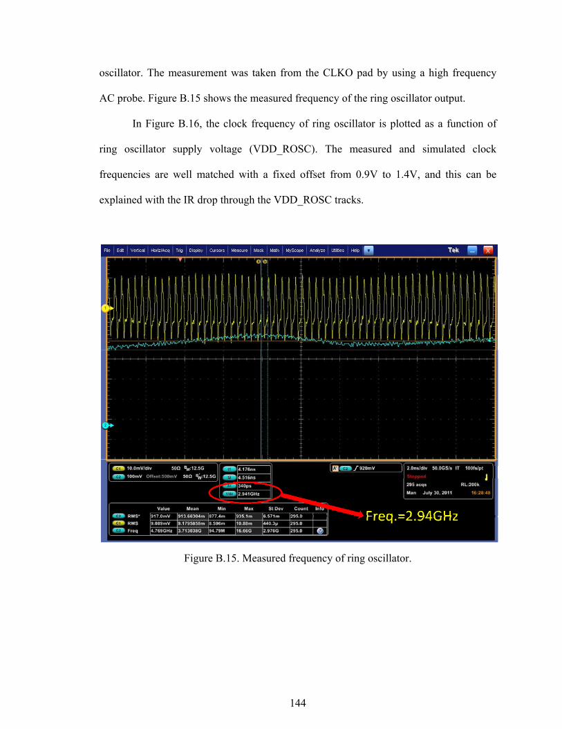
144
oscillator. The measurement was taken from the CLKO pad by using a high frequency
AC probe. Figure B.15 shows the measured frequency of the ring oscillator output.
In Figure B.16, the clock frequency of ring oscillator is plotted as a function of
ring oscillator supply voltage (VDD_ROSC). The measured and simulated clock
frequencies are well matched with a fixed offset from 0.9V to 1.4V, and this can be
explained with the IR drop through the VDD_ROSC tracks.
Figure B.15. Measured frequency of ring oscillator.
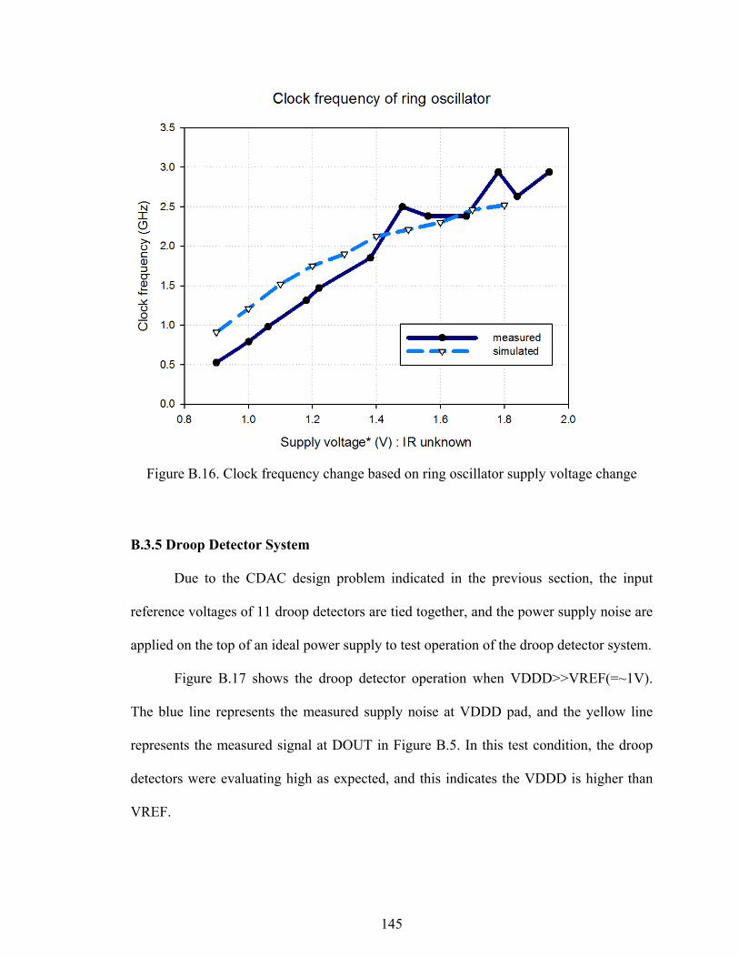
145
Figure B.16. Clock frequency change based on ring oscillator supply voltage change
B.3.5 Droop Detector System
Due to the CDAC design problem indicated in the previous section, the input
reference voltages of 11 droop detectors are tied together, and the power supply noise are
applied on the top of an ideal power supply to test operation of the droop detector system.
Figure B.17 shows the droop detector operation when VDDD>>VREF(=~1V).
The blue line represents the measured supply noise at VDDD pad, and the yellow line
represents the measured signal at DOUT in Figure B.5. In this test condition, the droop
detectors were evaluating high as expected, and this indicates the VDDD is higher than
VREF.
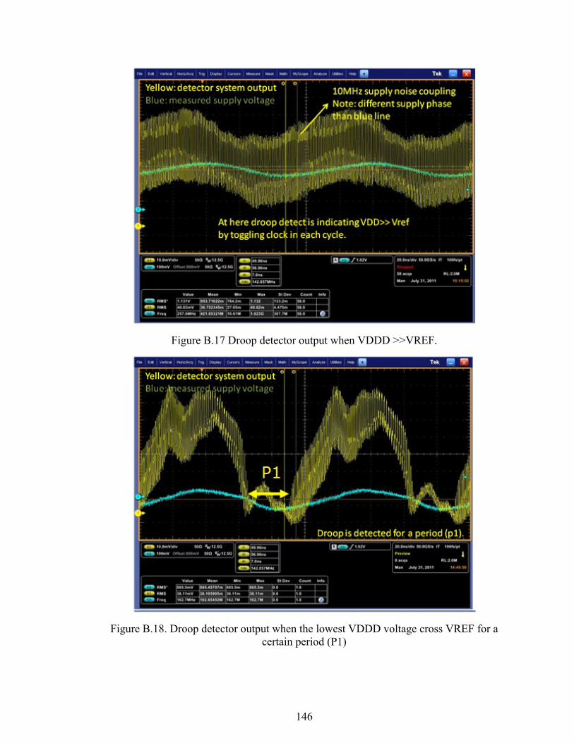
146
Figure B.17 Droop detector output when VDDD >>VREF.
Figure B.18. Droop detector output when the lowest VDDD voltage cross VREF for a certain period (P1)
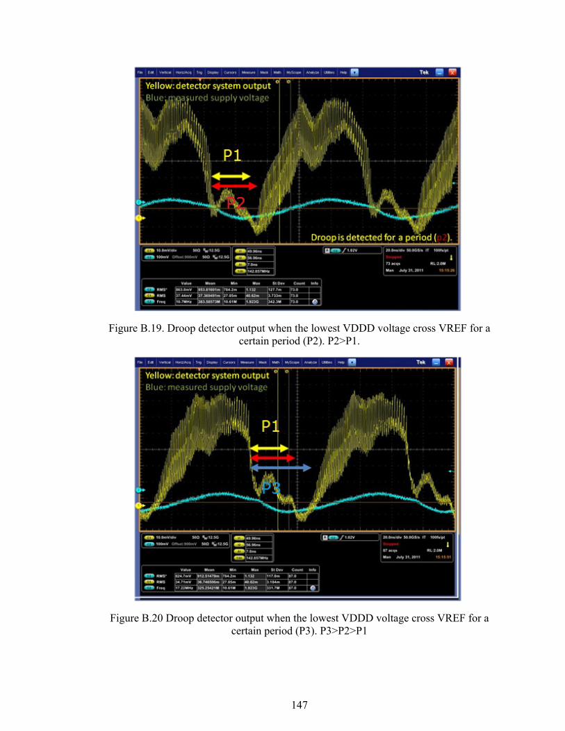
147
Figure B.19. Droop detector output when the lowest VDDD voltage cross VREF for a certain period (P2). P2>P1.
Figure B.20 Droop detector output when the lowest VDDD voltage cross VREF for a certain period (P3). P3>P2>P1
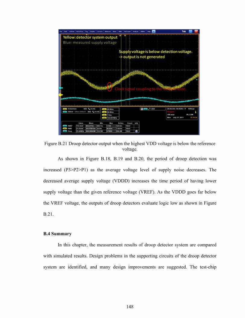
148
Figure B.21 Droop detector output when the highest VDD voltage is below the reference voltage.
As shown in Figure B.18, B.19 and B.20, the period of droop detection was
increased (P3>P2>P1) as the average voltage level of supply noise decreases. The
decreased average supply voltage (VDDD) increases the time period of having lower
supply voltage than the given reference voltage (VREF). As the VDDD goes far below
the VREF voltage, the outputs of droop detectors evaluate logic low as shown in Figure
B.21.
B.4 Summary
In this chapter, the measurement results of droop detector system are compared
with simulated results. Design problems in the supporting circuits of the droop detector
system are identified, and many design improvements are suggested. The test-chip
149
fabricated by IBM through MOSIS was found to be partially functional. The concept of
droop detector system was demonstrated with a workaround of the identified problems.
150
BIBLIOGRAPHY
[1] J. Jang, O. Franza, and W. Burleson, "Compact expressions for period jitter of global binary clock trees," in Proc. Electrical Performance of Electronic Packaging, 2008, pp. 47 - 50.
[2] J. Jang, O. Franza, and W. Burleson, "Period Jitter Estimation in Global Clock Trees," in Proc. IEEE Workshop on Signal Propagation on Interconnects, 2008, pp. 1-4.
[3] J. Jang, O. Franza, and W. Burleson, "Compact Expressions for Supply Noise Induced Period Jitter of Global Binary Clock Trees," IEEE Transactions On Very Large Scale Integration (VLSI) Systems, 2011.
[4] J. Jang and W. Burleson, "An Arbiter Based On-chip Droop Detector System," in ACM Great Lakes Symposium on VLSI (GLSVLSI), 2011.
[5] International Technology Roadmap for Semiconductors. [Online]. http://www.itrs.net/
[6] N. Kurd, J. Barkarullah, R. Dizon, T. Fletcher, and P. Madland, "A multigigahertz clocking scheme for the pentium(r) 4 microprocessor," IEEE Journal of Solide-Sate Circuits, vol. 36, no. 11, pp. 1647-1653, Nov 2001.
[7] N. Bindal, T. Kelly, N. Velastegui, and K. L. Wong, "Scalable sub-10ps skew global clock distribution for a 90nm multi-GHz IA microprocessor," in IEEE International Solid-State Circuits Conference, vol. 1, 2003, pp. 346-498.
[8] T. Fischer, F. Anderson, B. Patella, and S. Naffziger, "A 90nm variable-frequency clock system for a power-managed Itanium®-family processor," in IEEE International Solid-State Circuits Conference, 2005, pp. 294 - 599.
[9] S. Tam et al., "Clock Generation and Distribution of a Dual-Core Xeon Processor with 16MB L3 Cache," in IEEE International Solid-State Circuits Conference, 2006, pp. 1512-1521.
[10] N. Kurd, P. Mosalikanti, M. Neidengard, J. Douglas, and R. Kumar, "Next Generation Intel® Core™ Micro-Architecture (Nehalem) Clocking," IEEE Journal of Solid-State Circuits , vol. 44, no. 4, pp. 1121 - 1129 , April 2009.
[11] P. J. Restle et al., "A clock distribution network for microprocessors," IEEE Journal of Solid-State Circuits, vol. 36, no. 5, pp. 792-799, May 2001.
[12] Tektronix. Understanding and Characterizing Timing Jitter. [Online]. http://www.tek.com
[13] J. M. Rabey, A. Chandrakasan, and B. Nikolic, Digital Integrated Circuits: A design prespective, 3rd ed.: Prentice Hall.
[14] B. Razavi, Phase Locking in High-Performance Systems: From Devices to Architecture.: Wiley-IEEE Press, 2003.
[15] K. L. Wong, T. Rahal-Arabi, M. Ma, and G. Taylor, "Enhancing microprocessor immunity to power supply noise with clock-data compensation," IEEE Journal of Solid-State Circuits, vol. 41, no. 4, pp. 749-758, April 2006.
[16] A. Chandraksan, W. Bowhill, and F Fox, Design of High-Performance Microprocessor Circuits.: IEEE Press, 2001.
151
[17] M. Shah et al., "UltraSPARC T2: A highly-treaded, power-efficient, SPARC SOC," in IEEE Asian Solid-State Circuits Conference, 2007, pp. 22-25.
[18] N. Sakran et al., "The Implementation of the 65nm Dual-Core 64b Merom Processor," in IEEE International Solid-State Circuits Conference, 2007, pp. 106-590.
[19] N. Kurd, J. Douglas, P. Mosalikanti, and R. Kumar, "Next generation Intel® micro-architecture (Nehalem) clocking architecture," in IEEE Symposium on VLSI Circuits, 2008 , pp. 62 - 63.
[20] P. Mahoney, E. Fetzer, B. Doyle, and S. Naffziger, "Clock distribution on a dual-core, multi-threaded Itanium®-family processor," in IEEE International Solid-State Circuits Conference, 2005, pp. 292 - 599.
[21] T. Rahal-Arabi, G. Taylor, M. Ma, J. Jones, and C. Webb, "Design and validation of the core and IOs decoupling of the Pentium III and Pentium 4 processors," in Proc. Electrical Performance of Electronic Packaging, 2002, pp. 249-252.
[22] D. Jiao, J. Gu, P. Jain, and C. Kim, "Enhancing Beneficial Jitter Using Phase-Shifted Clock Distribution," in Proc. International Symposium on Low power electronics and design, 2008, pp. 21-26.
[23] D. Jiao, J. Gu, and C. Kim, "Circuit Techniques for Enhancing the Clock Data Compensation Effec under Resonant Supply Noise," in IEEE Custom Integrated Circuits Conference, Sep. 2009.
[24] M. Saint-Laurent and M. Swaminathan, "Impact of power-supply noise on timing in high-frequency microprocessors," IEEE Trans. Advanced Packaging, vol. 27, no. 1, pp. 135-144, Feb. 2004.
[25] J. Jang, S. Xu, and W. Burleson, "Jitter in deep sub-micron interconnect," in Proc. IEEE Computer Society Annual Symposium on VLSI, 2005, pp. 84-89.
[26] I. Kantorovich and C. Houghton, "Maximum Tolerable Power Supply Noise for Data-Clock Synchronization," in Proc. Electrical Performance of Electronic Packaging, Oct. 2006, pp. 167-170.
[27] L. Chen, M. Marek-Sadowska, and F. Brewer, "Coping with Buffer Delay Change Due to Power and Ground Noise," in Design Automation Conference, 2002.
[28] T. Xanthopoulos, Clocking in Modern VLSI Systems., 2009.
[29] E. G. Friedman, "Clock Distribution Networks in Synchronous Digital Integrated Circuits," Proc. IEEE, vol. 89, no. 5, pp. 665-692, May 2001.
[30] G. Gerosa, "A Sub 1W to 2W Low Power IA Processor for Mobile Internet Devices in 45nm Hi-K Metal Gate CMOS," IEEE Journal of Solid-State Circuits, vol. 44, no. 1, pp. 73-82, Jan. 2009.
[31] Predictive Technology Model, Arizona State Univeristy. [Online]. http://www.eas.asu.edu/~ptm
[32] S. R. Brain and et. al., "Low-k Interconnect Stack with a Novel Self-Aligned Via Patterning Process for 32nm High Volume Manufacturing," in IEEE International Interconnect Technology Conference, June, 2009, pp. 249-251.
[33] S. Pant and E. Chiprout, "Power grid physics and implications for CAD," in Proc. Design Automation Conference, 2006, pp. 199-204.
152
[34] N. Kurd and et. al., "Next Generation Intel Core™ Micro-Architecture (Nehalem) Clocking," IEEE Journal of Solid-State Circuits," IEEE Journal of Solid State Circuits, vol. 44, no. 4, pp. 1121-1129, April 2009.
[35] J. Jang, "Jitter in deep sub-micron interconnet," in Master's thesis, University of Massachusetts, Amherst, 2005.
[36] J. Roychowdhury, "Analyzing Circuits with Widely Separated Time Scales Using Numerical PDE Methods," IEEE Transactions on Circuits and Systems, vol. 48, no. 5, pp. 578-594, May 2001.
[37] M. Mansuri and C. K. Yang, "A Low-Power Adaptive Bandwidth PLL and Clock Buffer with Supply-Noise Compensation," IEEE Journal of Solid-StateCircuits, vol. 38, no. 11, pp. 1804-1812, Nov. 2003.
[38] E. Alon and et. al., "On-Die Power Supply Noise Measurement Techniques," IEEE Transactions on Advanced Packaging, May 2009.
[39] E. Alon, V. Stojanovic, and M.A. Horowitz, "Circuits and techniques for high-resolution measurement of on-chip power supply noise," IEEE Journal of Solid-State Circuits , vol. 40, no. 4, pp. 820 - 828, April 2005.
[40] S. Pant and D. Blaauw, "Circuit techniques for suppression and measurement of on-chip inductive supply noise," in Proc. European Solid-State Circuits Conference, 2008, pp. 134 - 137.
[41] C. Chansungsan, "Auto-referenced on-die power supply noise measurement circuit," in CICC, Sept 2005.
[42] M. S. A. Holtz, S. Narasimhan, and S. Bhunia, "On-die CMOS voltage droop detection and dynamic compensation," in GLVLSI, 2008.
[43] J. Tschanz and et. al., "Adaptive Frequency and Biasing Techniques for Tolerance to Dynamic Temperature-Voltage Variations and Aging," in ISSCC, Feb. 2007.
[44] R. Petersen and et. al., "Voltage Transient Detection and Induction for Debug and Test," in ITC, Sept. 2009.
[45] V. J. Reddi and et. al., "Voltage emergency prediction: Using signatures to reduce operating margins," in IEEE International Symposium on High Performance Computer Architecture, 2009, pp. 18-29.
[46] Intel, Intel® Pentium® 4 Processor in the 423-pin Package / Intel® 850 Chipset Platform Design Guide, Feb. 2002.
[47] Intel, Voltage Regulator Module (VRM) and Enterprise Voltage Regulator-Down (EVRD) 11.1 Design Guidelines, Sept. 2009.
[48] C. Foley, "Characterizing Metastability," IEEE Proc. Advanced Research in Asynchronous Circuits and System, Mar. 1996.
[49] D. Li, P. Chuang, and M. Sachdev, "Comparative Analysis and Study of Metastability on High-Performance Flip-Flops," in ISQED, Mar. 2010.
[50] S. Das and et. al., "RazorII: In Situ Error Detection and Correction for PVT and SER Tolerance," JSSC, Jan. 2009.
[51] V. Veetil, D, Sylvester, and D. Blaauw, "Efficient Monte Carlo based incremental statistical timing analysis," in Design Automation Conference, 2008, pp. 676-681.
153
[52] Mathworks. http://www.mathworks.com/products/simulink/.
[53] J. Dorsey and et. al., "An Integrated Quad-Core Opteron Processor," in ISSCC, 2007, pp. 102-103.
[54] R. E. Best, Phase Locked Loops. Design, Simulations, and Applications, 6th ed.: McGraw-Hill, 2007.
[55] F. M. Gardner, PHASELOCK TECHNIQUES.: A JOHN WILEY & SONS, 2005.
[56] N. Kurd and P. Mosalikanti, "Power-efficient scalable multi core and high-speed IO clocking architecture," in CMOSET, 2009.
[57] A. Iyer, "Phase Synthesis Using Coupled Phase-Locked Loops," University of Massachusetts, Amherst, Masters Theses 2008.
[58] J. G. Maneatis, "Low-Jitter Process-Independent DLL and PLL Based on Self-Biased Techniques," IEEE Journal of Solid-State Cricuits, vol. 31, no. 11, pp. 1723-1732, Nov. 1996.
[59] B. Razzavi, Design of Analog CMOS Integrated Circuits , 1st ed.: McGraw-Hill Science/Engineering/Math, 2000.
[60] V. Pavlidis, I. Savidis, and E.G. Friedman, "Clock distribution networks for 3-D ictegrated Circuits," in IEEE Custom Integrated Circuits Conference, 2008.
[61] X. Zhao and S. Lim, "Power and slew-aware clock network design for through-silicon-via (TSV) based 3D ICs," in Proceedings of the 2010 Asia and South Pacific Design , 2010.
[62] D. Jiao, T. Kim, J. Keane, and C. Kim, "A Multi-Story Power Delivery Technique for 3D Integrated Circuits," in International Symposium on Low Power Electronics and Design , 2008.
[63] M. B. Healy and S. Lim, "A study of stacking limit and scaling in 3D ICs: an interconnect perspective," in IEEE Electronic Components and Technology Conference, 2009, 2009.
[64] V. Arunachalam and W. Burleson, "Low-Power Clock Distribution in a Multilayer Core 3D Microprocessor," in ACM Great Lakes Synposium on VLSI, 2008.
[65] K. Chillara, J. Jang, and W. Burleson, "Robust Signaling Techniques for Through Silicon Vias Bundles," in ACM Great Lakes Symposium on VLSI, 2011.
[66] K. Yoon and et. al., "Modeling and Analysis of Coupling between TSVs, Metal, and RDL interconnects in TSV-based 3D IC with Silicon Interposer," in Electronics Packaging Technology Conference, 2009.
[67] Intel. (2009) An Introduction to the Intel QuickPath Interconnect. [Online]. http://www.intel.com/technology/quickpath/introduction.pdf
[68] D. Blaauw, R. Panda, and R. Chaudhry, "Design and analyis of power distribution networks," in Design of High-Performance Microprocessor Circuits.: IEEE Press, 2001, ch. 24, pp. 499-522.
[69] D. W. Bailey and B. J. Benschneider, "Clocking design and analysis for a 600-MHz Alpha microprocessor," IEEE Journal of Solid-State Circuits, vol. 33, no. 11, pp. 1627-1633, Nov 1998.
154
[70] S. Taylor, "The challenge of designing global signals in USDM CMOS," in Proc. IEEE Custom Integrated Circuits, 1999, pp. 419-435.
[71] M. Mansuri and C. K. Yang, "A low-power adaptive bandwidth PLL and clock buffer with supply-noise compensation," IEEE Journal of Solid-State Circuits, vol. 38, no. 11, pp. 1804-1812, Nov 2003.
[72] V. A. Abramzon, E. Alon, B. Nezamfar, and M. Horowitz, "Scalable circuits for supply noise measurement," in Proc. European Solid-State Circuits Conference, 2005, pp. 463 - 466.
[73] A. Muhtaroglu, G. Taylor, and T. Rahal-Arabi, "On-die droop detector for analog sensing of power supply noise," IEEE Journal of Solid-State Circuits , vol. 39, no. 4, pp. 651 - 660, April 2004.
[74] A. M. Abas et al., "Time difference amplifier," Electronics Letters, vol. 38, no. 23, pp. 1437-1438, Nov. 2002.
[75] M. Lee and A. A. Abidi, "A 9 b, 1.25 ps Resolution Coarse–Fine Time-to-Digital Converter in 90 nm CMOS that Amplifies a Time Residue," IEEE Journal of Solid-State Circuits, vol. 43, no. 4, pp. 769 - 777 , April 2008.
[76] A. Sehgal, P. Song, and K. A. Jenkins, "On-chip Real-Time Power Supply Noise Detector," in Proc. European Solid-State Circuits Conference, 2006 , pp. 380 - 383.