Embed Size (px)
Citation preview
*A preliminary shorter version of this paper was published in the Proceedings of the 2012 IEEE International Symposium on Multiple-Valued Logic.
Clock Distribution Area Reduction Using a Multiple-Valued Clocking Approach*
Rohit P Menon Mitchell A Thornton Department of Computer Science and Engineering Department of Computer Science and Engineering
Southern Methodist University Southern Methodist University Dallas, Texas, USA Dallas, Texas, USA
[email protected] [email protected] Abstract – Multi-phase clocking methods are well known and widely used in high-performance integrated circuit design. Such a scheme allows for relaxation of timing constraints among disjoint partitions of the logic circuitry since lower frequency local clocking is required as compared to the system clock frequency at the cost of increased clock distribution network area. The disadvantage is that multiple clock distribution trees are required, one for each clock domain or phase within the integrated circuit. Clock distribution networks have the highest fanout of any circuit within typical ICs and represent a significant amount of resource utilization. We devise a method that retains the advantages of multi-phase IC design, but utilizes a single global multiple-valued clock signal distribution network versus separate distribution networks for each phase in an ASIC or custom VLSI implementation. The technique requires a minimal amount of modification to existing multi-phase designs and is evaluated and compared to traditional multiphase designs. Furthermore, the approach is applicable to programmable logic (FPGA) implementations through distributing the multiple-valued clock signal using log2(N) distribution networks for an N-phase system. Experimental results are provided to validate and evaluate the approach.
1. INTRODUCTION
Increasing the performance of Integrated Circuits (ICs) is of paramount concern to support advances in technology. Many techniques are employed for increasing performance, ranging from new and improved fabrication technology to advances in design techniques. One design approach is that of partitioning a globally clocked synchronous logic circuit into disjoint subcircuits referred to as ‘phases.’ Each phase then utilizes a private clock distribution network with a substantially reduced clock frequency. However, overall performance does not degrade since the multiple subcircuits may all operate concurrently. This approach, referred to here as ‘Multi-phase clocking’ is a form of pipelining since it incorporates temporal concurrency. Pipelining is a well-known digital design performance enhancement technique whereby concurrency is exploited in a temporal sense as opposed to physical duplication of functional units [16]. While multi-phase clocking has the advantage of retaining high-performance while relaxing timing constraints within
each subcircuit phase domain, the significant disadvantage is that multiple clock distribution networks must be provided for each phase clock instead of a single global clock distribution network. Such clock distribution networks are a well-known source of power dissipation and overall area utilization. We describe a method for implementing the concept of multi-phase clocking that only requires a single clock distribution network. The chief concept utilized in this approach is that of a Multiple-Valued Logic (MVL) global clock signal. MVL concepts have been devised and used by circuit designers [1,2,3,5] and also developers of Electronic Design Automation (EDA) tools for digital circuit simulation and synthesis. MVL circuitry is attractive for high-speed IC designs as reduction in chip area, increase in performance, and reduced power dissipation characteristics are major requirements for future ICs. Clocking is an essential concept in the design of synchronous digital systems [10]. A synchronous system is comprised of storage elements and combinational logic that together make up a Finite State Machine (FSM) controller and a datapath. A typical clock signal has to be distributed to a large number of storage elements and hence it usually has the highest fan-out of any node in a typical digital design. As a result, a clock distribution system alone can consume up to 25-70% of the power budget of the IC chip [4,17,18,19,20]. Clocking in digital systems continues to gain importance since the clock frequency is increasing rapidly, approximately doubling every three years. The increase in clock uncertainties due to higher clock frequencies has made designing clock distributions in high-performance microprocessors and other ICs increasingly difficult. Hence distributed multi-phase clock systems can play a vital role in high-performance circuit designs where independent clock networks with lower frequency non-overlapping clock signals are physically distributed to disjoint subsets of the clocked storage elements. Many high-performance digital integrated circuits being produced today use multi-phase clock distribution systems [7,8,9]. The clock distribution networks used in multi-phase clock distribution systems require a significant amount of resources in terms of area since each clock phase requires an independent distribution network. Difficulties also arise in maintaining synchronization among the independent clock phases. Such high performance digital integrated circuits typically use multi-phase clock distribution systems with
level-sensitive latches as clocked storage elements. A set of N periodic non-overlapping binary clock signals propagate over each of the clock phase distribution networks and drive disjoint subsets of level-sensitive latches providing enhanced throughput and performance. This performance enhancement can result in increased area characteristics since the individual distribution networks are required for each clock phase. Other current approaches in overcoming challenges in clocking include the use of reference-based distribution architectures [22] involving multi-tap distribution lines. Another approach modifies the binary clock signal to have a swing of one-half Vdd in an attempt to decrease power consumption [23]. The half-swing approach has some similarity to the method described here in that overall clock signal voltage amplitudes are modified. Level-sensitive transparent latches [6] as state-holding elements provide high-performance and low power consumption [13] as compared to flip-flops. Level-sensitive latches are attractive since they require fewer transistors to implement as compared to edge-sensitive storage devices. However, the transparent nature of latches increases the difficulty in meeting timing criteria as compared to the use of edge-sensitive circuits. Because timing constraints are considerably relaxed within each subcircuit of a multi-phased clocked logic design, latches are more easily used and are often the state-holding element of choice for these types of designs. The MVL-based method presented here implements the strategy of a multi-phase clocking architecture but utilizes a single clock distribution network instead of multiple clock distribution networks [14,15]. The single clock distribution network contains a multi-valued logic clock signal propagating to all clocked storage elements present in the high-performance IC. The single network may be implemented as a single conductor that distributes an MV clock signal encoded as a set of discrete voltage levels, or as a set of log(N) conductors distributing a binary encoded version of the MV clock signal. The approach described here is formulated with the intent of reducing required area for multi-phase synchronous integrated circuit designs. Area reduction is achieved by replacing the N multiple clock distribution networks needed for each phase in a conventional approach with a single distribution network in an ASIC implementation or with log2(N) networks for a binary implementation. The challenges with respect to timing closure due to large scale distribution of high-frequency clock signals will remain, however, we compensate for the use of a more complicated clock signal by a reduction in overall frequency and through the use of level-sensitive storage devices instead of edge-sensitive devices. For explanatory purposes, this paper focuses on a four-valued voltage-mode quaternary clock signal (i.e. four logic levels - logic 0, logic 1, logic 2 and logic 3). Binary level-sensitive latches are augmented to contain a modified literal selection gate inserted in-line between the MV clock signal input and the gating input of the latch. There are four different modified literal selection gates that correspond to one of each
of the four clock phase domains. The output of the modified literal selection gate is a standard binary signal that produces a logic-1 for one of the four MV clock signal levels and a logic-0 otherwise. The paper is organized as follows: In Section 2, the background of the approach is described and the application to custom or standard cell integrated circuits as a target technology is included. In Section 3, an alternative implementation of the approach is described that allows for the use of only binary logic elements through the use of a bundled set of log(N) conductors that distribute an encoded version of the MV clock signal. The approach of Section 3 does not require the implementation of custom MV subcircuits, but does require more clock distribution network area; however, it is reduced from N independent multi-phase binary clock signals to log(N) binary signals. In Section 4, experimental results supporting the technique are provided. Finally in Section 5, conclusions are provided.
2. CUSTOM OR STANDARD CELL IC IMPLEMENTATION
A typical high performance IC design with multiple phase clock signal distribution networks is depicted in Fig 1. An on-chip Phase Locked Loop (PLL) receives the binary external clock input to generate a stable high frequency global clock signal that is then input to a multi-phase clock generation circuit. The phase generation circuit produces each of the N lower frequency individual clock phase signals that are in turn distributed to a subset of latches in each phase domain. CDTi represents the individual distribution networks.
Fig 1. Block Diagram of Multi-phase Clocking
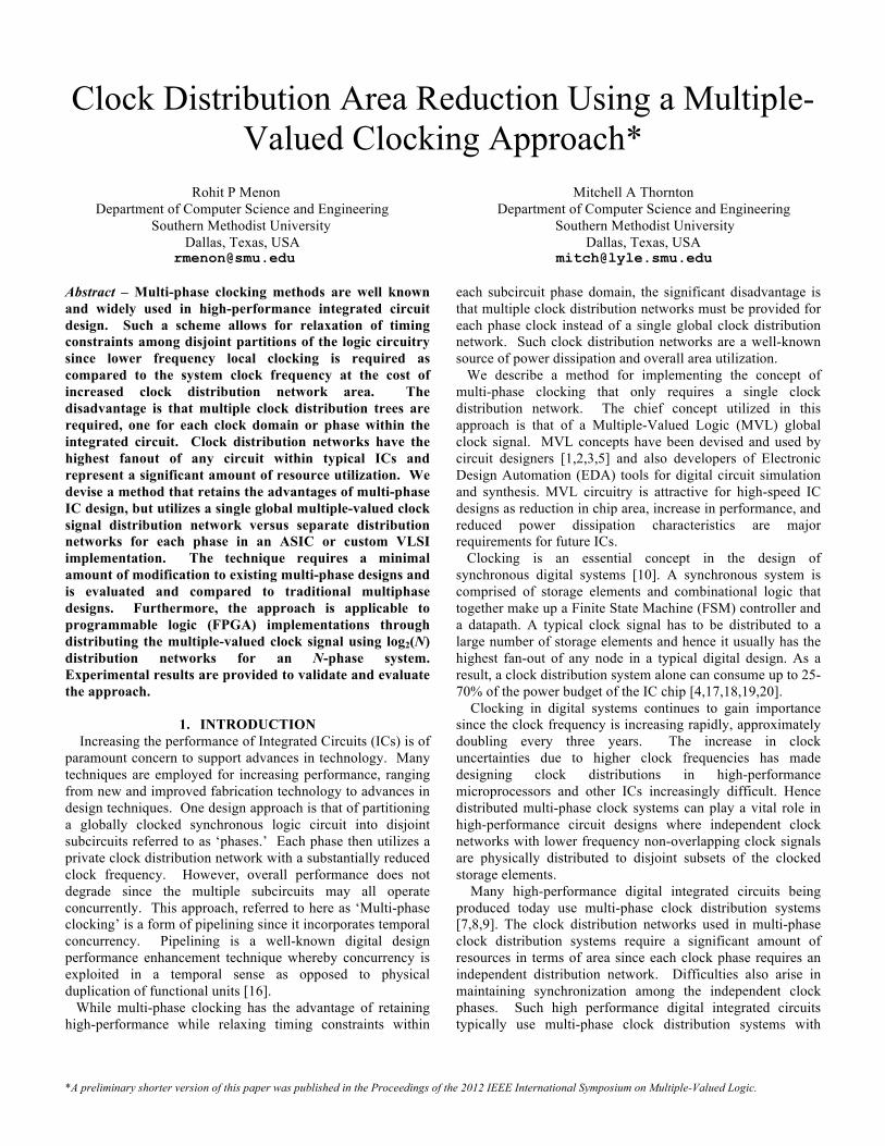
In Fig 1, the N multiple phase shifted clock signals are represented by Φ0, Φ1,.., ΦN-1. In terms of quaternary logic, we consider four phase shifted clock signals, represented by Φ0, Φ1, Φ2 and Φ3. An example of the clock signal waveforms for the external global clock input and the resulting four phase shifted clock signals are shown in Fig 2. The four multiple non-overlapping phase shifted clock signals, Φ0, Φ1, Φ2 and Φ3, propagate to disjoint sets of sub-circuits over corresponding Clock Distribution Tree (CDT) networks. Each sub-circuit shown in Fig 1 is comprised of combinational logic along with sequential logic elements which are typically level-sensitive transparent latches.
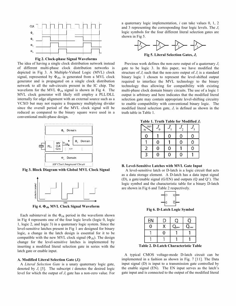
Fig 2. Clock-phase Signal Waveforms
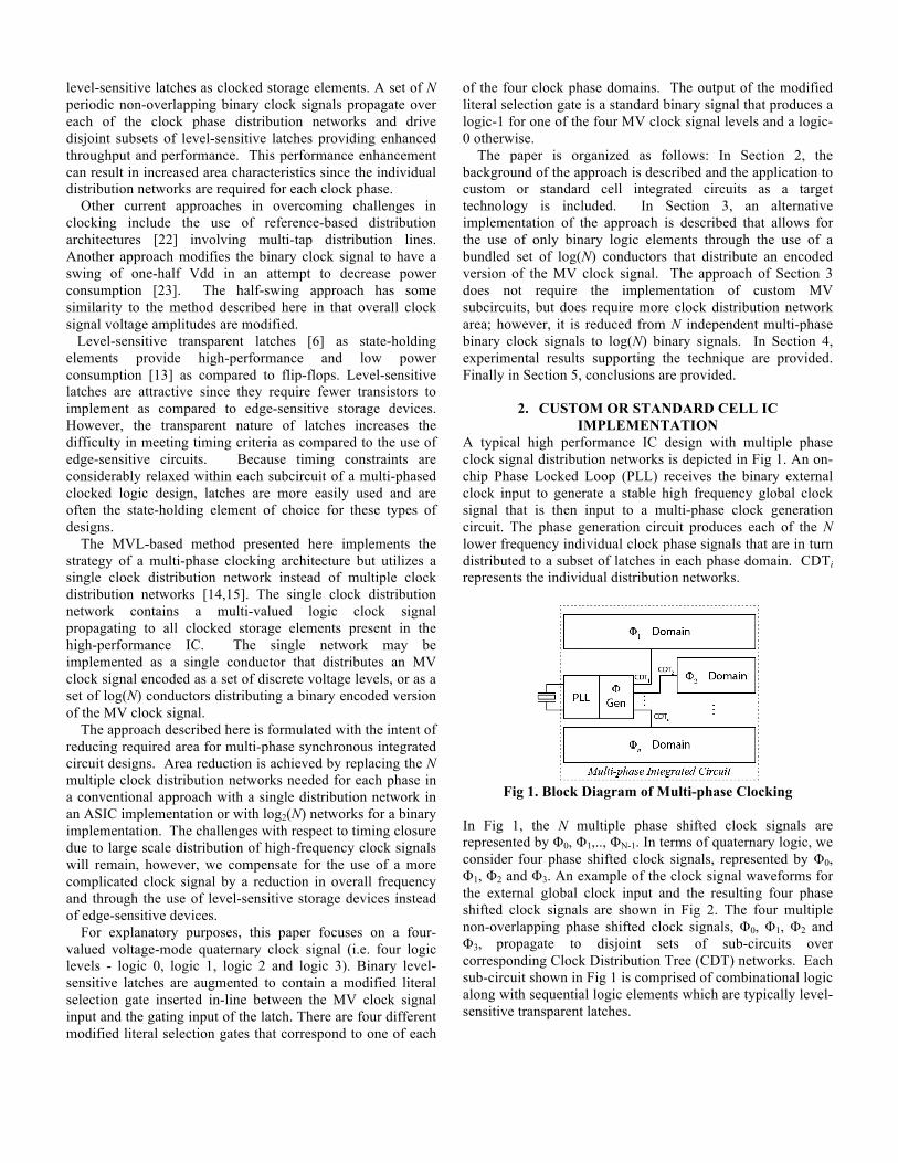
The idea of having a single clock distribution network instead of different multi-phase clock distribution networks is depicted in Fig 3. A Multiple-Valued Logic (MVL) clock signal, represented by Φclk, is generated from a MVL clock generator and is propagated on a single clock distribution network to all the sub-circuits present in the IC chip. The waveform for the MVL Φclk signal is shown in Fig 4. The MVL clock generator will likely still employ a PLL/DLL internally for edge alignment with an external source such as a VCXO but may not require a frequency multiplying divider since the overall period of the MVL clock signal will be reduced as compared to the binary square wave used in a conventional multi-phase design.
Fig 3. Block Diagram with Global MVL Clock Signal
Fig 4. Φclk MVL Clock Signal Waveform
Each subinterval in the Φclk period in the waveform shown in Fig 4 represents one of the four logic levels (logic 0, logic 1, logic 2, and logic 3) in a quaternary logic system. Since the level-sensitive latches present in Fig 1 are designed for binary logic, a change in the latch design is essential for it to be compatible with the new MVL clock signal (Φclk). The design change for the level-sensitive latches is implemented by inserting a modified literal selection gate in series with the latch gate or enable input. A. Modified Literal Selection Gate (Ji) A Literal Selection Gate is a unary quaternary logic gate, denoted by Ji [5]. The subscript i denotes the desired logic level for which the output of Ji gate has a non-zero value. For
a quaternary logic implementation, i can take values 0, 1, 2 and 3 representing the corresponding four logic levels. The Ji logic symbols for the four different literal selection gates are shown in Fig 5.
Fig 5. Literal Selection Gates, Ji
Previous work defines the non-zero output of a quaternary Ji gate to be logic 3. In this paper, we have modified the structure of Ji such that the non-zero output of Ji is a standard binary logic 1 chosen to represent the level-shifted output required to interface the MVL technology to the binary technology thus allowing for compatibility with existing multi-phase clock domain binary circuits. The use of a logic 1 output is arbitrary and here indicates that the modified literal selection gate may contain appropriate level-shifting circuitry to enable compatibility with conventional binary logic. The modified literal selection gate, Ji is defined as shown in the truth table in Table 1.
Table 1. Truth Table for Modified Ji
B. Level-Sensitive Latches with MVL Gate Input A level-sensitive latch or D-latch is a logic circuit that acts as a data storage element. A D-latch has a data input signal (D), a gate/enable signal (G/EN) and outputs (Q and Q’). The logic symbol and the characteristic table for a binary D-latch are shown in Fig 6 and Table 2 respectively.
Fig 6. D-Latch Logic Symbol
Table 2. D-Latch Characteristic Table
A typical CMOS voltage-mode D-latch circuit can be implemented in a fashion as shown in Fig. 7 [11]. The Data input signal (D) is input to a transmission gate controlled by the enable signal (EN). The EN input serves as the latch’s gate input and is connected to the output of the modified literal
selection gate. The output of the transmission gate is connected to a latch comprised of two inverters where the topmost inverter serves as a keeper logic circuit.
Fig 7. Typical Voltage-Mode D-Latch Circuit
To generate the MV global clock signal for a multi-phase clock domain circuit, the PLL and phase generation circuit shown in Fig 1 are replaced by a subcircuit labeled MVL clock generator as shown in Fig 3. The individual CDT distribution networks are replaced with a single global MV clock signal distribution network and an appropriate modified literal selection circuit is inserted in series with the EN input of the transparent D-latches. Area savings results in a custom or standard cell implementation through the replacement of the multiple CDT networks with a single clock distribution network since routing and via placement is less complex. Depending on which CDT domain is used, each original D-latch is replaced with one of the four sub-circuits shown in Fig 8 comprising a modified literal selection gate in series with the D-latch EN input.
Fig 8. D-latches with Modified Literal Selection Gates
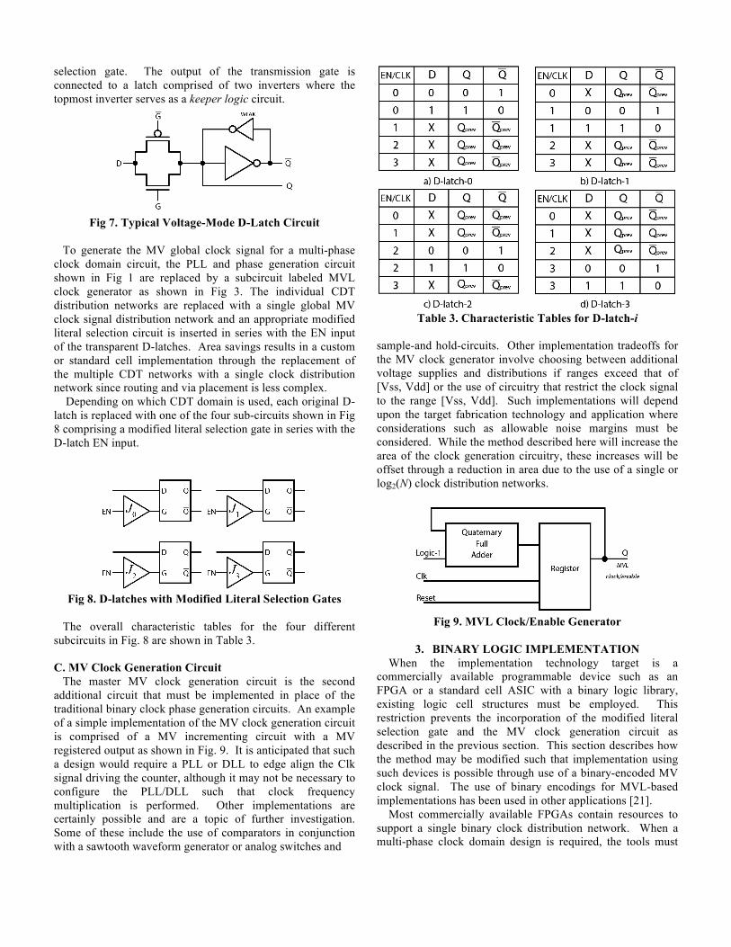
The overall characteristic tables for the four different subcircuits in Fig. 8 are shown in Table 3. C. MV Clock Generation Circuit The master MV clock generation circuit is the second additional circuit that must be implemented in place of the traditional binary clock phase generation circuits. An example of a simple implementation of the MV clock generation circuit is comprised of a MV incrementing circuit with a MV registered output as shown in Fig. 9. It is anticipated that such a design would require a PLL or DLL to edge align the Clk signal driving the counter, although it may not be necessary to configure the PLL/DLL such that clock frequency multiplication is performed. Other implementations are certainly possible and are a topic of further investigation. Some of these include the use of comparators in conjunction with a sawtooth waveform generator or analog switches and
Table 3. Characteristic Tables for D-latch-i
sample-and hold-circuits. Other implementation tradeoffs for the MV clock generator involve choosing between additional voltage supplies and distributions if ranges exceed that of [Vss, Vdd] or the use of circuitry that restrict the clock signal to the range [Vss, Vdd]. Such implementations will depend upon the target fabrication technology and application where considerations such as allowable noise margins must be considered. While the method described here will increase the area of the clock generation circuitry, these increases will be offset through a reduction in area due to the use of a single or log2(N) clock distribution networks.
Fig 9. MVL Clock/Enable Generator
3. BINARY LOGIC IMPLEMENTATION
When the implementation technology target is a commercially available programmable device such as an FPGA or a standard cell ASIC with a binary logic library, existing logic cell structures must be employed. This restriction prevents the incorporation of the modified literal selection gate and the MV clock generation circuit as described in the previous section. This section describes how the method may be modified such that implementation using such devices is possible through use of a binary-encoded MV clock signal. The use of binary encodings for MVL-based implementations has been used in other applications [21]. Most commercially available FPGAs contain resources to support a single binary clock distribution network. When a multi-phase clock domain design is required, the tools must
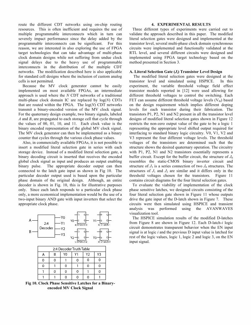
route the different CDT networks using on-chip routing resources. This is often inefficient and requires the use of multiple programmable interconnects which in turn can severely impact performance since the delay added by the programmable interconnects can be significant. For this reason, we are interested in also exploring the use of FPGA target technologies that can take advantage of multi-phase clock domain designs while not suffering from undue clock signal delays due to the heavy use of programmable interconnects in the distribution of the multiple CDT networks. The modification described here is also applicable for standard cell designs where the inclusion of custom analog cells is not permitted. Because the MV clock generator cannot be easily implemented on most available FPGAs, an intermediate approach is used where the N CDT networks of a traditional multi-phase clock domain IC are replaced by log(N) CDTs that are routed within the FPGA. The log(N) CDT networks transmit a binary-encoded version of the MV clock signal. For the quaternary design example, two binary signals, labeled A and B, are propagated to each storage cell that cycle through the values of 00, 01, 10, and 11. Each clock value is the binary encoded representation of the global MV clock signal. The MV clock generator can then be implemented as a binary counter that cycles through the various clock phase values. Also, in commercially available FPGAs, it is not possible to insert a modified literal selection gate in series with each storage device. Instead of a modified literal selection gate, a binary decoding circuit is inserted that receives the encoded global clock signal as input and produces an output enabling binary pulse. The appropriate decoder output can then connected to the latch gate input as shown in Fig 10. The particular decoder output used is based upon the particular phase domain of the original design. Although, an entire decoder is shown in Fig. 10, this is for illustrative purposes only. Since each latch responds to a particular clock phase only, a more economical implementation would be the use of a two-input binary AND gate with input inverters that select the appropriate clock phase.
Fig 10. Clock Phase Sensitive Latches for a Binary-
encoded MV Clock Signal
4. EXPERIMENTAL RESULTS Three different types of experiments were carried out to validate the approach described in this paper. The modified literal selection gates were designed and implemented at the transistor level, several multi-phase clock domain synchronous circuits were implemented and functionally validated at the RTL level, and several different circuits were designed and implemented using FPGA target technology based on the method presented in Section 3. A. Literal Selection Gate (Ji) Transistor Level Design The modified literal selection gates were designed at the transistor level and simulated using HSPICE. In this experiment, the variable threshold voltage field effect transistor models reported in [12] were used allowing for different threshold voltages to control the switching. Each FET can assume different threshold voltage levels (Vth) based on the design requirement which implies different doping levels for each transistor during their fabrication. The transistors P1, P2, N1 and N2 present in all the transistor level designs of modified literal selection gates shown in Figure 12 restricts the non-zero output value of the gate to be a logic 1 representing the appropriate level shifted output required for interfacing to standard binary logic circuitry. V0, V1, V2 and V3 represent the four different voltage levels. The threshold voltages of the transistors are determined such that the structure shows the desired quaternary operation. The circuitry with P1, P2, N1 and N2 transistors essentially represents a buffer circuit. Except for the buffer circuit, the structure of J0 resembles the static-CMOS binary inverter circuit and structure of J3 is a series connection of two J0 structures. The structures of J1 and J2 are similar and it differs only in the threshold voltages chosen for the transistors. Figure 11 contains circuit diagrams for the four literal selection gates. To evaluate the viability of implementation of the clock phase sensitive latches, we designed circuits consisting of the four literal selection gate shown in Figure 11 whose outputs drive the gate input of the D-latch shown in Figure 7. These circuits were then simulated using HSPICE and transient analysis was performed using the AVANWAVES visualization tool. The HSPICE simulation results of the modified D-latches from Figure 8 are shown in Figure 12. Each D-latch-i logic circuit demonstrates transparent behavior when the EN input signal is at logic i and the previous D input value is latched for rest of the logic values, logic 1, logic 2 and logic 3, on the EN input signal.
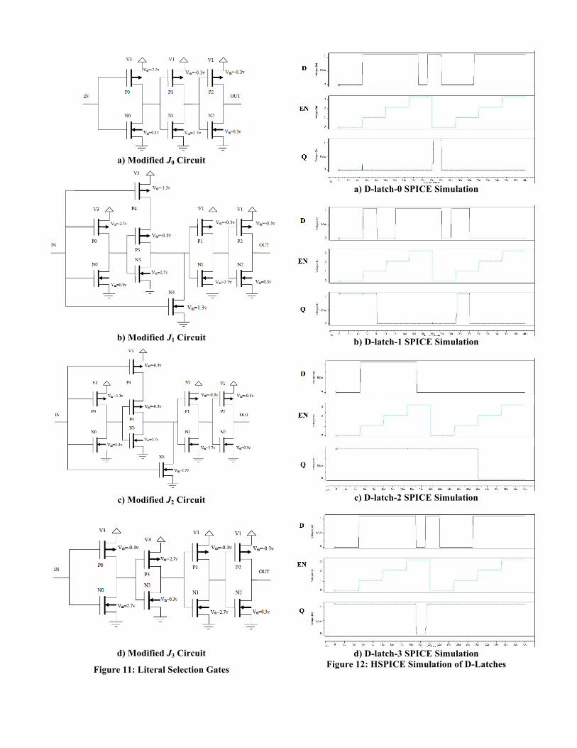
a) Modified J0 Circuit
b) Modified J1 Circuit
c) Modified J2 Circuit
d) Modified J3 Circuit
Figure 11: Literal Selection Gates
a) D-latch-0 SPICE Simulation
b) D-latch-1 SPICE Simulation
c) D-latch-2 SPICE Simulation
d) D-latch-3 SPICE Simulation
Figure 12: HSPICE Simulation of D-Latches
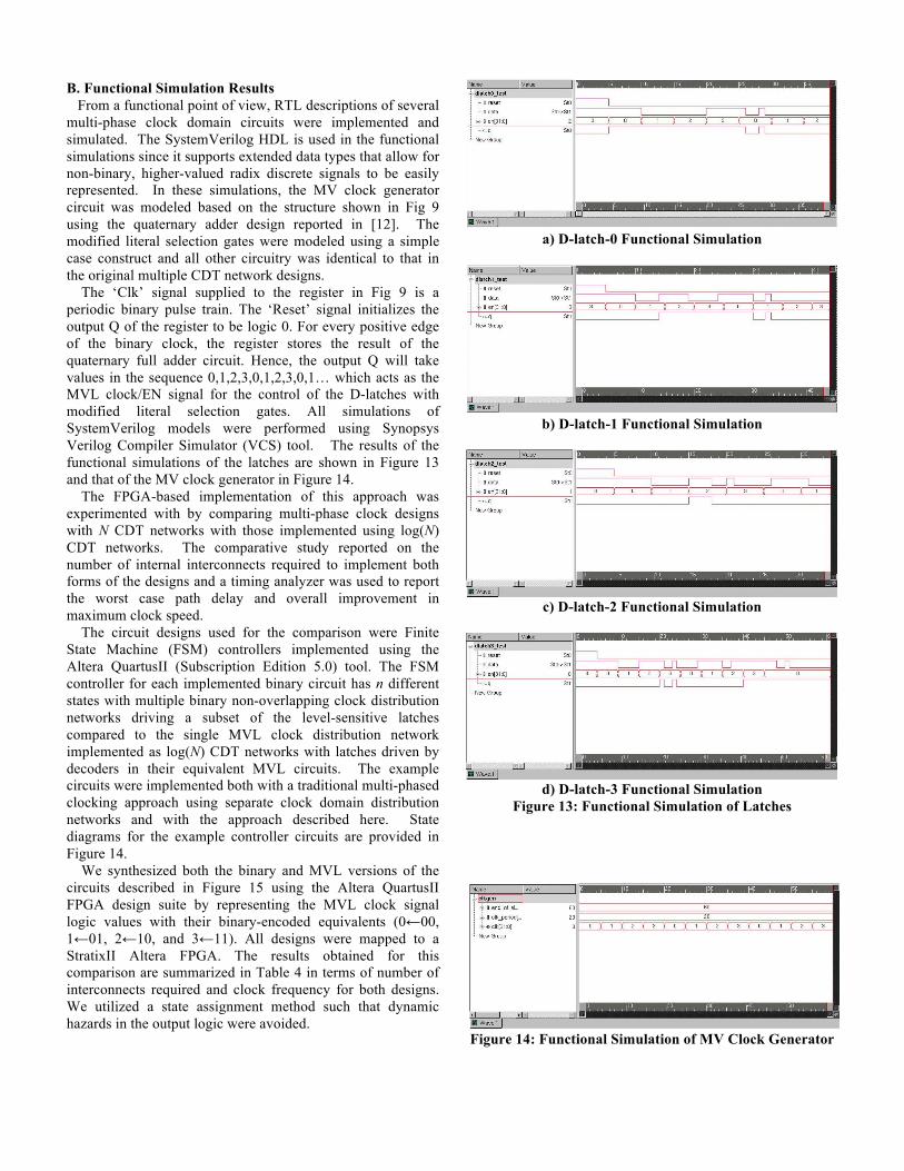
B. Functional Simulation Results From a functional point of view, RTL descriptions of several multi-phase clock domain circuits were implemented and simulated. The SystemVerilog HDL is used in the functional simulations since it supports extended data types that allow for non-binary, higher-valued radix discrete signals to be easily represented. In these simulations, the MV clock generator circuit was modeled based on the structure shown in Fig 9 using the quaternary adder design reported in [12]. The modified literal selection gates were modeled using a simple case construct and all other circuitry was identical to that in the original multiple CDT network designs. The ‘Clk’ signal supplied to the register in Fig 9 is a periodic binary pulse train. The ‘Reset’ signal initializes the output Q of the register to be logic 0. For every positive edge of the binary clock, the register stores the result of the quaternary full adder circuit. Hence, the output Q will take values in the sequence 0,1,2,3,0,1,2,3,0,1… which acts as the MVL clock/EN signal for the control of the D-latches with modified literal selection gates. All simulations of SystemVerilog models were performed using Synopsys Verilog Compiler Simulator (VCS) tool. The results of the functional simulations of the latches are shown in Figure 13 and that of the MV clock generator in Figure 14. The FPGA-based implementation of this approach was experimented with by comparing multi-phase clock designs with N CDT networks with those implemented using log(N) CDT networks. The comparative study reported on the number of internal interconnects required to implement both forms of the designs and a timing analyzer was used to report the worst case path delay and overall improvement in maximum clock speed. The circuit designs used for the comparison were Finite State Machine (FSM) controllers implemented using the Altera QuartusII (Subscription Edition 5.0) tool. The FSM controller for each implemented binary circuit has n different states with multiple binary non-overlapping clock distribution networks driving a subset of the level-sensitive latches compared to the single MVL clock distribution network implemented as log(N) CDT networks with latches driven by decoders in their equivalent MVL circuits. The example circuits were implemented both with a traditional multi-phased clocking approach using separate clock domain distribution networks and with the approach described here. State diagrams for the example controller circuits are provided in Figure 14. We synthesized both the binary and MVL versions of the circuits described in Figure 15 using the Altera QuartusII FPGA design suite by representing the MVL clock signal logic values with their binary-encoded equivalents (0←00, 1←01, 2←10, and 3←11). All designs were mapped to a StratixII Altera FPGA. The results obtained for this comparison are summarized in Table 4 in terms of number of interconnects required and clock frequency for both designs. We utilized a state assignment method such that dynamic hazards in the output logic were avoided.
a) D-latch-0 Functional Simulation
b) D-latch-1 Functional Simulation
c) D-latch-2 Functional Simulation
d) D-latch-3 Functional Simulation
Figure 13: Functional Simulation of Latches
Figure 14: Functional Simulation of MV Clock Generator
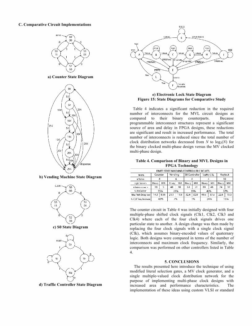
C. Comparative Circuit Implementations
a) Counter State Diagram
b) Vending Machine State Diagram
c) S0 State Diagram
d) Traffic Controller State Diagram
e) Electronic Lock State Diagram
Figure 15: State Diagrams for Comparative Study Table 4 indicates a significant reduction in the required number of interconnects for the MVL circuit designs as compared to their binary counterparts. Because programmable interconnect structures represent a significant source of area and delay in FPGA designs, these reductions are significant and result in increased performance. The total number of interconnects is reduced since the total number of clock distribution networks decreased from N to log2(N) for the binary clocked multi-phase design versus the MV clocked multi-phase design.
Table 4. Comparison of Binary and MVL Designs in FPGA Technology
The counter circuit in Table 4 was initially designed with four multiple-phase shifted clock signals (Clk1, Clk2, Clk3 and Clk4) where each of the four clock signals drives one particular state to another. A design change was then made by replacing the four clock signals with a single clock signal (Clk), which assumes binary-encoded values of quaternary logic. Both designs were compared in terms of the number of interconnects and maximum clock frequency. Similarly, the comparison was performed on other controllers listed in Table 4.
5. CONCLUSIONS The results presented here introduce the technique of using modified literal selection gates, a MV clock generator, and a single multiple-valued clock distribution network for the purpose of implementing multi-phase clock designs with increased area and performance characteristics. The implementation of these ideas using custom VLSI or standard
cell ASIC target technology is described including a discussion of the supporting new subcircuits required. Functional validations of several designs were accomplished using the SystemVerilog HDL and a transistor-level design and simulation was carried out using the HSPICE simulator. We described how these ideas could be adapted for implementation in commercially available FPGA devices or ASICS based on binary-only logic cells and described how the new subcircuits could be replaced using standard binary components such as a modular counter in place of the master clock generator and a binary decoder in place of the modified literal selection gate. Experimental results show improved performance and reduction in area for a set of example circuits when these ideas are applied as compared to their binary counterparts. This set of experimental results was obtained by using the Altera QuartusII EDA tool to implement several example circuits.
REFERENCES [1] Epstein, G., Frieder, G., and Rine, D.C., “The
Development of Multiple-Valued Logic as Related to Computer Science”, IEEE Computer, vol. 7, pp. 20-32, 1974.
[2] Smith, K.C., “The Prospects for Multivalued Logic: A Technology and Application View,” IEEE Trans Computers, vol. 30, pp. 619-634, 1981.
[3] Hurst, S.L., “Multiple-Valued Logic-Its Status and Its Future,” IEEE Trans. Computers, vol. 33, no. 12, pp. 1,160-1,179, Dec. 1984.
[4] Gronowski P.E, et. al, “High-performance microprocessor design,” IEEE Journal of Solid-State Circuits, vol. 33, iss. 5, May 1998.
[5] Miller, D.M. and Thornton, M.A., Mutiple-Valued Logic: Concepts and Representations, Morgan & Claypool Publishers, San Rafael, CA, ISBN 10-1598291904, 2008.
[6] Gong, M., Zhou, H., Li, L., Tao, J., & Zeng, X., “Binning Optimization for Transparently-Latched Circuits”, IEEE Transactions on Computer-Aided Design of Integrated Circuits and Systems, 30(2), 270-283, 2011.
[7] Eby, G. and Friedman, “Clock Distribution Networks in Synchronous Digital Integrated Circuits,” Proc. of IEEE, vol. 89, no. 5, 2001, pp. 665 –692.
[8] Jackson, M.A.B. and Srinivasan, A., et. al., “Clock Routing for High-Performance ICs,” Proc. of ACM/IEEE Design Automation Conf., pp. 573-579, 1990.
[9] Papaefthymiou, M.C. and Randall, K.H., “TIM: A timing Package for two-phase, level-clocked circuitry,” in Proc. of ACM/IEEE Design Automation Conf., 1993, pp. 497–502.
[10] Oklobdzija, V.G., Stojanovic, V.M., Markovic, D.M. and Nedovic, N.M., Digital System Clocking: High-Performance and Low-Power Aspects, John Wiley & Sons, Inc. ISBN: 0-471-27447-X, 2003.
[11] Vasundara P. and Gurumurthy, K.S., “Static Random Access Memory Using Quaternary Latch”, Int. Jour. of Eng. Sci. and Tech., 2(11), 2010, 6371-6379.
[12] Datla, S., Thornton, M.A., Hendrix, L., and Henderson, D., “Quaternary addition circuits based on SUSLOC voltage-mode cells and modeling with SystemVerilog,” Proc. of IEEE Int. Sym. on Multiple-Valued Logic, pp. 256-261, 2009.
[13] Ebeling, C. and Lockyear, B. “On the performance of level-clocked circuits,” in Proc. Advanced Research in VLSI, Chapel Hill, NC, 1995, pp. 342–356.
[14] Menon, R.P. and Thornton, M.A., “Global Multiple-valued Clock Approach for High-performance Multi-phase Clock Integrated Circuits,” in Proc. of IEEE Int. Symposium on Multiple-Valued Logic, pp. 19-24, 2012.
[15] Menon, R.P. and Thornton, M.A., “Single Clock Distribution Network for Multi-Phase Clock Integrated Circuits,” U.S. Patent Pending, Provisional Patent 61/599,598, February 2012.
[16] Kogge, P.M., The Architecture of Pipelined Computers, McGraw-Hill Publishing, 1981, ISBN 9780070352377.
[17] El-Moursy, M.A. and Friedman, E.G., “Exponentially Tapered H-Tree Clock Distribution Networks,” IEEE Trans. VLSI, vol. 13, no. 8, 2005, pp. 971-975.
[18] Nedovic, N. and Oklobdzija, “Dual-Edge Triggered Storage Elements and Clocking Strategy for Low-Power Systems,” IEEE Trans. VLSI, vol. 13, no. 5, 2005, pp. 577-590.
[19] Zhao, X., Minz, J. and Lim, S.K., “Low-Power and Reliable Clock Network Design for Through-Silicon Via (TSV) Based 3D ICs,” IEEE Trans. Comp., Pkg., and Man. Tech., vol. 1, no. 2, 2011, pp. 247-255.
[20] Santhanum, S. et al., “A Low-Cost, 300 MHz, RISC CPU with Attached Media Processor,” IEEE Jour. Solid-State Circ., vol. 33, no. 11, 1998, pp. 1829-1839.
[21] Sasao, T., “Multiple-Valued Logic and Optimization of Programmable Logic Arrays,” IEEE Computer Magazine, 1988, pp. 71-80.
[22] Chattopadhyay, A. and Zilic, Z., “Reference-Based Clock Distribution Architectures,” in Proc. IEEE Midwest Symposium on Circ. and Sys., 2006, pp. 704-708.
[23] Kojima, H., Tanaka, S., and Sasaki, K., “Half-Swing Clocking Scheme for 75% Power Saving in Clocking Circuitry,” in Proc. IEEE Symposium on VLSI Circ., 1994, pp. 23-24.