Embed Size (px)
Citation preview

CL-PD6710/’22
Preliminary Data Sheet
Version 3.1
OVERVIEW
FEATURES
■
Single-chip PC Card host adapters
■
Direct connection to ISA (PC AT) bus and one or two PC Card sockets
■
Compliant with PC Card Standard, PCMCIA 2.1, and JEIDA 4.1
■
82365SL-compatible register set, ExCA
-compatible
■
Automatic Low-Power Dynamic mode for lowest active power consumption
■
Programmable Suspend mode
■
Hardware-enabled Super Suspend mode
■
Five programmable memory windows per socket and two programmable I/O windows per socket
■
Programmable card access cycle timing
■
8- or 16-bit system bus interface
■
8- and 16-bit PC Card interface support
■
ATA disk interface support
■
DMA support (CL-PD6722)
■
Card-voltage sense support
■
PC Card activity indicator
■
Mixed-voltage operation (3.3/5.0 V)
■
Single-socket interface: 144-pin VQFP for smallest form factor (CL-PD6710)
■
Dual-socket interface: 208-pin PQFP or VQFP (CL-PD6722)
ISA–to–PC-Card Host Adapters
System Block Diagram
ISA (AT)BUS
CL-PD6710
144-Pin
CL-PD6722
208-Pin
The CL-PD6710 and CL-PD6722 are single-chip PCCard host adapter solutions capable of controllingone (CL-PD6710) or two (CL-PD6722) PC Cardsockets. The chips are compliant with PC Card Stan-dard, PCMCIA 2.1, and JEIDA 4.1 and are optimizedfor use in notebook and handheld computers wherereduced form factor and low power consumption arecritical design objectives. With the CL-PD6710, acomplete PC Card solution with power-control logiccan occupy less than 1.5 square inches (excludingthe socket connector). With the CL-PD6722, a com-plete dual-socket PC Card solution with power-con-trol logic can occupy less than 2 square inches(excluding socket connectors).
The chips employ energy-efficient mixed-voltagetechnology that can reduce system power consump-tion by over 50 percent. The chips also provide: aLow-Power Dynamic mode, which automaticallystops the internal clock during periods of card inac-tivity; a software-controlled Suspend mode, whichdramatically reduces power by disabling most of theinternal circuitry and stopping data transactions tothe PC Cards; and a hardware-controlled Super Sus-pend mode, which reduces current to the µA range.(cont.)
May 1997
PC CARD SOCKET 1
PC CARD SOCKET 2
...............................
...............................
PC C
ard
...............................
...............................
PC C
ard
(CL-PD6722)

CL-PD6710/’22
ISA–to–PC-Card Host Adapters
OVERVIEW
(cont.)
Personal computer applications typically access PCCards through a third-party socket/card-servicessoftware interface. To assure full compatibility withindustry-standard socket/card-services software andPC Card applications, the register set in theCL-PD6710 and CL-PD6722 is a superset of theIntel 82365SL register set.
2
Notebook Computer Design Priorities
■ Small Form Factor
■ Minimum Power Consumption
■ High Performance
■ Compatibility
Host Adapter Form Factor
Card
1 3/8"
CL-PD6710144-Pin VQFP1"
VCC
VPP
and
Switch-
Cir-ing
cuitry
The chips provide fully buffered PC Card interfaces,meaning that no external logic is required for buffer-ing signals to/from the interface, and power con-sumption can be controlled by limiting signaltransitions on the PC Card bus.
PRELIMINARY DATA SHEET v3.1May 1997
Supporting Features
❒ Single-chip solutions
❒ No external buffers for host or socket
❒ Efficient board layout
❒ Automatic Low-Power Dynamic mode
❒ Hardware- and software-controlled Suspend modes
❒ Mixed-voltage operation
❒ Write cache
❒ Programmable timing supports more cards, faster reads and writes
❒ Automatic bus sizing for 8- or 16-bit
❒ DMA available with the CL-PD6722
❒ Compliant with PC Card Standard, PCMCIA 2.1, and JEIDA 4.1
❒ 82365SL A-step register-compatible, ExCA -compatible
CL-PD6722208-Pin
1 9/16"
1 1/
4"
Card
VCC
VPP
and
Switch-
Cir-
ing
cuitry
PQFP or VQFP

CL-PD6710/’22
ISA–to–PC-Card Host Adapters
Table of Contents
1. GENERAL CONVENTIONS.................. 7
2. PIN INFORMATION............................... 82.1 Pin Diagrams .....................................................92.2 Pin Description Conventions............................112.3 Pin Descriptions...............................................122.4 Power-On Configuration Summary ..................21
3. INTRODUCTION.................................. 223.1 System Architecture.........................................223.1.1 PC Card Basics ............................................223.1.2 CL-PD67XX Windowing Capabilities ............223.1.3 CL-PD67XX Functional Blocks.....................253.1.4 Interrupts ......................................................253.1.5 Alternate Functions of Interrupt Pins ............263.1.6 General-Purpose Strobe Feature .................263.1.7 Voltage Sense Pins.......................................273.1.8 CL-PD67XX Power Management .................273.1.9 Socket Power Management Features...........283.1.10 Write FIFO....................................................293.1.11 Bus Sizing.....................................................293.1.12 Programmable PC Card Timing....................293.1.13 ATA Mode Operation.....................................293.1.14 DMA Mode Operation for
the CL-PD6722.............................................303.1.15 Selective Data Drive for I/O Windows...........303.2 Host Access to Registers.................................303.3 Power-On Setup...............................................31
4. REGISTER DESCRIPTION CONVENTIONS................................... 32
5. OPERATION REGISTERS.................. 335.1 Index ................................................................335.2 Data .................................................................36
6. CHIP CONTROL REGISTERS............ 376.1 Chip Revision...................................................376.2 Interface Status................................................386.3 Power Control ..................................................406.4 Interrupt and General Control ..........................426.5 Card Status Change ........................................446.6 Management Interrupt Configuration ...............456.7 Mapping Enable ...............................................47
7. I/O WINDOW MAPPINGREGISTERS ........................................ 49
7.1 I/O Window Control ..........................................497.2 System I/O Map 0–1 Start Address Low..........507.3 System I/O Map 0–1 Start Address High.........507.4 System I/O Map 0–1 End Address Low...........517.5 System I/O Map 0–1 End Address High ..........51
7.6 Card I/O Map 0–1 Offset Address Low............527.7 Card I/O Map 0–1 Offset Address High ...........52
8. MEMORY WINDOW MAPPING REGISTERS .........................................53
8.1 System Memory Map 0–4 Start Address Low ..................................................................53
8.2 System Memory Map 0–4 Start Address High..................................................................54
8.3 System Memory Map 0–4 End Address Low ..................................................................54
8.4 System Memory Map 0–4 End Address High..................................................................55
8.5 Card Memory Map 0–4 Offset Address Low ..................................................................56
8.6 Card Memory Map 0–4 Offset Address High..................................................................56
9. EXTENSION REGISTERS...................589.1 Misc Control 1 ..................................................589.2 FIFO Control ....................................................609.3 Misc Control 2 ..................................................619.4 Chip Information...............................................639.5 ATA Control ......................................................649.6 Extended Index ................................................659.7 Extended Data .................................................659.7.1 Data Mask 0–1 .............................................669.7.2 Extension Control 1 (CL-PD6722 only,
formerly DMA Control) ..................................669.7.3 Maximum DMA Acknowledge Delay
(CL-PD6722 only) .........................................679.7.4 External Data (CL-PD6722 only, Socket A,
Index 2Fh).....................................................699.7.5 External Data (CL-PD6722 only, Socket A,
Index 6Fh).....................................................709.7.6 Extension Control 2 (CL-PD6722 only) ........71
10. TIMING REGISTERS ...........................7210.1 Setup Timing 0–1.............................................7210.2 Command Timing 0–1......................................7310.3 Recovery Timing 0–1 .......................................74
11. ATA MODE OPERATION.....................75
12. USING GPSTB PINS FOR EXTERNAL PORT CONTROL (CL-PD6722 only) ..77
12.1 Control of GPSTB Pins ....................................7712.2 Example Implementations of GPSTB-Controlled
Read and Write Ports.......................................7912.3 GPSTB in Suspend Mode................................80
13. VS1# AND VS2# VOLTAGE DETECTION .........................................81
May 1997 3PRELIMINARY DATA SHEET v3.1
CL-PD6710/’22
ISA–to–PC-Card Host Adapters
14. DMA OPERATION (CL-PD6722 only)................................ 83
14.1 DMA Capabilities of the CL-PD6722 ...............8314.2 DMA-Type PC Card Cycles .............................8314.3 ISA Bus DMA Handshake Signal.....................8414.4 Configuring the CL-PD6722 Registers for
a DMA Transfer ................................................8414.4.1 Programming the DMA Request Pin from
the Card........................................................8514.4.2 Configuring the Socket Interface for I/O .......8614.4.3 Preventing Dual Interpretation of DMA
Handshake Signals.......................................8614.4.4 Turning On DMA System..............................8614.5 The DMA Transfer Process ..............................8614.6 Terminal Count to Card at Conclusion
of Transfer .......................................................86
15. ELECTRICAL SPECIFICATIONS ....... 8715.1 Absolute Maximum Ratings .............................8715.2 DC Specifications ............................................8715.3 AC Timing Specifications .................................9115.3.1 ISA Bus Timing .............................................9215.3.2 Reset Timing.................................................9415.3.3 System Interrupt Timing................................95
15.3.4 General-Purpose Strobe Timing (CL-PD6722 only).........................................96
15.3.5 Input Clock Specification ..............................9715.3.6 PC Card Bus Timing Calculations ................9815.3.7 PC Card Socket Timing ................................99
16. PACKAGE SPECIFICATIONS........... 11016.1 144-Pin VQFP Package .................................11016.2 208-Pin PQFP Package.................................11116.3 208-Pin VQFP Package .................................112
17. ORDERING INFORMATION EXAMPLE.......................................... 113
A. Using the Cirrus Logic BBS and FTP Server................................. 114
B. Register Summary Tables ............... 116B.1 Operation Registers .......................................116B.2 Chip Control Registers...................................116B.3 I/O Window Mapping Registers .....................118B.4 Memory Window Mapping Registers .............119B.5 Extension Registers.......................................120B.6 Timing Registers............................................123
INDEX ................................................ 124
PRELIMINARY DATA SHEET v3.1May 19974

CL-PD6710/’22
ISA–to–PC-Card Host Adapters
Document Revision History
Version 3.1Following are major changes between September 1995and May 1997 versions of this data sheet:General
The CL-PD6710 replaces the CL-PD6712, which wastaken out of production. This change is reflected through-out this data sheet. Major differences of the CL-PD6710from the CL-PD6712 include:
The CL-PD6710 does not support DMA.Only a single voltage sense pin is available.GPSTB functionality is not supported.
References to the CL-PD6720 were removed. Refer-ences to the CL-PD672X were replaced with CL-PD6722.
For the CL-PD6710, two pin names were changed fromthe CL-PD6712 to reflect their different functionality:
VS1#/A_GPSTB is now 5V_DET.VS2#/B_GPSTB is now a no connect.
Section
2.2 The General-Purpose Strobe/Voltage Sense pinsin the CL-PD6712 (VS1#/A_GPSTB andVS2#/B_GPSTB) were replaced by the 5V_DETin the CL-PD6710.
5.1 The Extended Index and Extended Data registers(Scratchpad, Data Mask 0, Data Mask 1, Exten-sion Control 1, Maximum DMA AcknowledgeDelay, Reserved, External Data, and ExtensionControl 2) are only available on the CL-PD6722,not on the CL-PD6710.
13 Voltage detection on the CL-PD6710 is providedby the 5V_DET pin.
Version 3.0Following are major changes between July 1994 andSeptember 1995 versions of this data sheet:
General
A new chip was added: the CL-PD6712, whichreplaces the CL-PD6710.
Extended register set was expanded.
208-pin VQFP package option was added for theCL-PD6720 and CL-PD6722.
Some windowing register names were changedto specify either card or system.
References to PCMCIA card were changed to PCCard.
The chips are compatible with PC Card Standard,as R2 PC Card controllers.
May 1997PRELIMINARY DATA SHEET v3.1
For the CL-PD6712, two pin names are differentthan the CL-PD6710 to reflect new functionality:
5V_DET became VS1#/A_GPSTBN.C./RESERVED became VS2#/B_GPSTB
For the CL-PD672X, two pin names werechanged to reflect new functionality:
A_5V_DET became A_GPSTBB_5V_DET became B_GPSTB
For the CL-PD67XX, four pin names werechanged to reflect their full functionality:
IRQ12 became IRQ12/LED_OUT*IRQ15 became IRQ15/RI_OUT*BVD1/-STSCHG became BVD1/-STSCHG/-RIBVD2/-SPKR became BVD2/-SPKR/-LED
For the CL-PD67XX, two pin names were changedto match other Cirrus Logic PC Card products:
SLOT_VCC became SOCKET_VCCVDD became CORE_VDD
Section
2.2 I/O type codes changed.
2.3 Table columns rearranged, power control pinsplaced in their own table.Table added for general-purpose strobe / voltagesense pins.
3.1.2 Windowing figures added.
3.1.3 Functional block figure added.
3.1.5 More information about LED_OUT*, RI_OUT*,DACK*, and DRQ alternate functions of interruptpins added.
3.1.6 Section on general-purpose strobe added.
3.1.7 Section on voltage sense added.
3.2 Sample code for accessing registers added.
4 Read/Write Convention table added.
6.3 Auto-Power bit description changed.
6.4 IRQ Level bits name changed to Card IRQ Select.
6.6 Management IRQ bits name changed to Manage-ment IRQ Select.
9.1 5V Detect (bit 0 of index 16h) is now Reserved.
9.4 Chip Identification (bits 7:6 of index 1Fh) is nownamed Cirrus Logic Host-Adapter Identification.
9.7 External Data and Extension Control 2 regis-ters added.LED Activity Enable bit added to Extension Con-trol 1 register. Auto Power Clear bit namechanged to Auto Power Clear Disable.
10 ‘11’ value of Prescalar Select bits of timing regis-ters changed to 8192.
5TABLE OF CONTENTS

CL-PD6710/’22ISA–to–PC-Card Host Adapters
For Command Multiplier Value bits, order of resetstates for Timing sets 0 and 1 switched to showreset state for Timing set 0 first.Recovery Timing register reset value changed to03h to allow additional I/O cycle recovery time ofsystems using ’DX/4 processors.
11 ATA information is now in an application note.
12 General-purpose strobe chapter added.
13 Voltage sense chapter added.
15.1 Allowable voltage on any pin increased to ±0.5 Vgreater than voltage of +5V pin.
15.3 Table 15-7: values for t2, t2a, t10, t13, and t18 ofISA bus timing table changed.Table 15-9: Pulse mode interrupt timing added.Table 15-10: General-purpose strobe timingadded.Table 15-12: values of t5 and t6 of memoryread/write timing table changed.Table 15-13: -WAIT timing values added to wordI/O read/write timing.Table 15-17 and 15-18: DMA read and write cycletiming tables expanded.
16 208-pin VQFP package added.
Version 2.5Following are major changes between October1993 and July 1994 versions of this data sheet:General
An extension register and two bits have beenadded to the CL-PD6722 register set.
Section
1.2 Description for bits labeled Reserved, Compatibil-ity, 0 or 1, and Scratchpad have been clarified.
5.2 In the table for “Bits 1-0: Battery Voltage Detect”,the column headings for bit 1 and bit 0 werereversed, and have been corrected.
5–7 Bits 6, 3, and 2 (index 2h), bits 6 and 2 (index 7h),and bit 6 (index 11h, 19h, 21h, 29h, 31h) havebeen relabeled Compatibility bits.
6.6 Bit 0 (index 36h, 38h) has been relabeled 0.
8.4 Bit 1 (index 1Fh) has been changed to be a partof the CL-PD67XX Revision Level field. Bit 0 hasbeen relabeled Reserved.
8.7 Two bits, Auto-Power Clear and VCC Power Lock,and a register, Maximum DMA AcknowledgeDelay, have been added to descriptions of theCL-PD6722 registers. The DMA Control registerwas renamed Extension Control 1. The DisableSocket Pull-Ups bit was renamed Pull-Up Control.
11.3 References to -WE and -OE in the last paragraphhave been corrected.
11.4.1The table on DMA signal usage and Figure 11-2have been slightly modified.
13 The 144- and 208-pin package drawings havebeen updated.
Version 2Following are major changes between January1993 and October 1993 versions of this data sheet:General
A new chip was added: the CL-PD6722.
The CL-PD672X packaging name was changedto PQFP; the physical package is the same.
The chips are also compatible with PCMCIA 2.1.
Section
2.2 SPKR_OUT*/CSEL pin description in Table 2-1was changed from TO-PU type to IO-PU type.Addition of the CL-PD6722 chip changed descrip-tion in Tables 2-1 and 2-2 of the following pins:IRQ9, IRQ10, -VPP_VALID, -REG, -OE, -WE,WP/-IOIS16, -INPACK, and BVD2/-SPKR.
3.1 The typical power consumption values in Table3-1 were updated (reduced) to more closelyreflect expected values.Sections 3.1.10 and 3.1.11 are new sectionsdescribing the CL-PD6722.
5–9 Many indications of Constant bits in registerswere changed from “0” to “Scratch Bit”.
5 In the Card Status Change register, the BatteryDead/STSCHG Enable bit name was renamedBattery Dead Or Status Change Enable.
8 The Misc Control 2 register bit 6 is not reservedon the CL-PD6722. Its functionality is described.Sections 8.6 and 8.7 were added to describeCL-PD6722–specific registers.
9 The Setup, Command, and Recovery field nameswere altered. The default state for the CommandMultiplier Value field was corrected. The timingformulas for all three timing register sets werereformatted. The timing with ‘11’ values selectedon the Prescalar Select field calculate differently.
11 This new chapter descr ibes DMA on theCL-PD6722.
12 Extensive changes were made throughout thischapter. Please review carefully.
PRELIMINARY DATA SHEET v3.1May 19976
TABLE OF CONTENTS

CL-PD6710/’22ISA–to–PC-Card Host Adapters
1. GENERAL CONVENTIONS
The following general conventions apply to this doc-ument.
Throughout this document, CL-PD67XX meansCL-PD6710 and CL-PD6722.
Bits within words and words within various memoryspaces are generally numbered with a 0 (zero) asthe least-significant bit or word. For example, theleast-significant bit of a byte is bit 0, while the most-significant bit is bit 7.
In addition, number ranges for bit fields and wordsare presented with the most-significant value first.Thus, when discussing a bit field within a register,the bit number of the most-significant bit is writtenfirst, followed by a colon (:) and then the bit numberof the least-significant bit; as in, bits 7:0.
In this document, the names of the CL-PD67XXinternal registers are boldfaced. For example, ChipRevision and Power Control are register names.The names of bit fields are written with initial upper-case letters. For example, Card Power On and Bat-tery Voltage Detect are bit field names.
May 1997PRELIMINARY DATA SHEET v3.1
Numbers and Units
The unit Kbyte designates 1024 bytes (210). The unitMbyte designates 1,048,576 bytes (220). The unitGbyte designates 1,073,741,824 bytes (230). Theunit Hz designates hertz. The unit kHz designates1000 Hz. The unit MHz designates 1,000,000 Hz.The unit ms designates millisecond. The unit µsdesignates microsecond. The unit ns designatesnanosecond. The unit mA designates milliampere.The unit V immediately following a number desig-nates volt.
Hexadecimal numbers are presented with all lettersin uppercase and a lowercase h appended. Forexample, 14h and 03CAh are hexadecimal num-bers.
Binary numbers are enclosed in single quotationmarks when in text. For example, ‘11’ is a binarynumber.
Numbers not appended with an h nor enclosed bysingle quotation marks are decimal.
In addition, a capital letter X is used within numbersto indicate digits ignored by the CL-PD67XX withinthe current context. For example, ‘101XX01’ is abinary number with bits 3:2 ignored.
7GENERAL CONVENTIONS

CL-PD6710/’22ISA–to–PC-Card Host Adapters
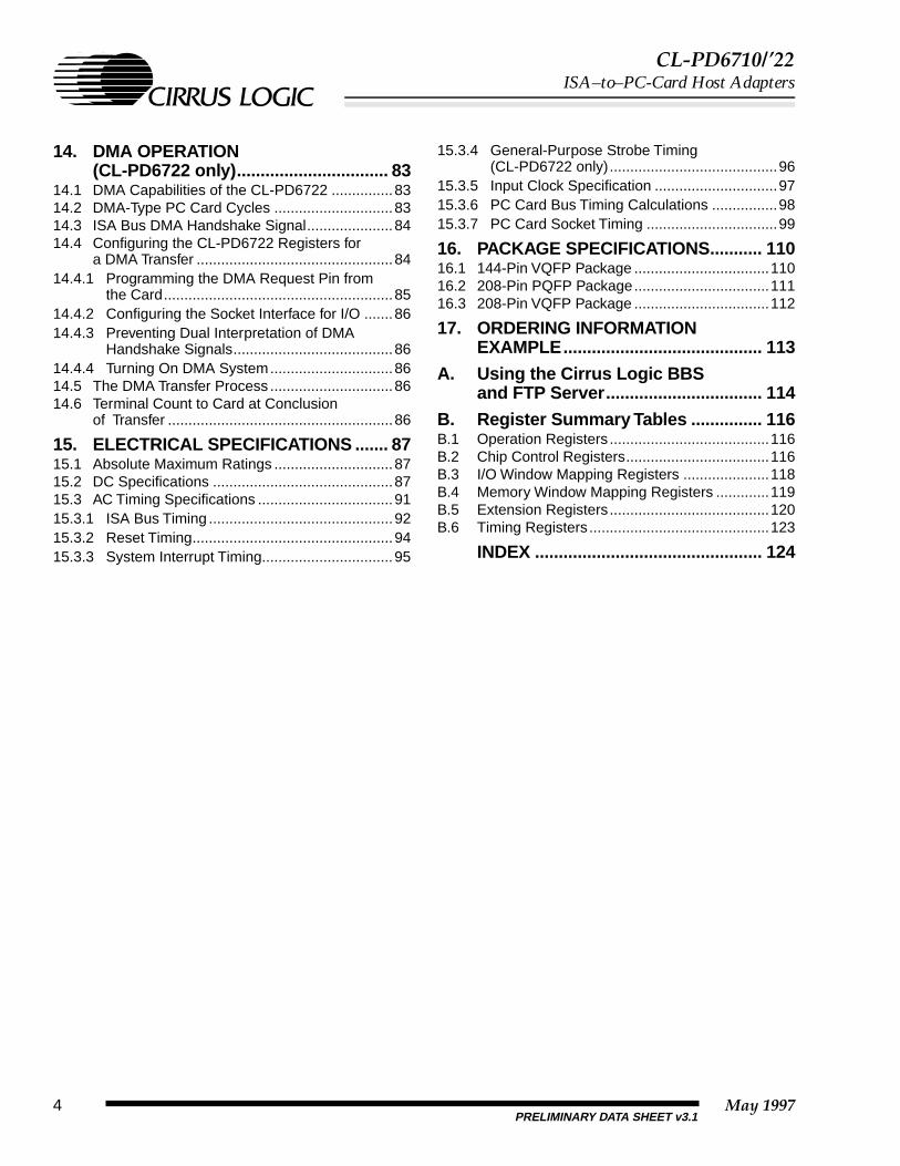
2. PIN INFORMATION
The CL-PD6710 is available in a 144-pin VQFP (very tight-pitch quad flat pack) component package andthe CL-PD6722 is available in either a 208-pin PQFP (plastic quad flat pack) component package or a208-pin VQFP component package. The interface pins can be divided into five groups:
● ISA bus interface pins
● PC Card socket interface pins (one or two sets)
● General-purpose strobe / voltage sense pins
● Power control pins
● Power and ground pins
Refer to Figure 2-1 for the CL-PD6710 and Figure 2-2 for the CL-PD6722 pin diagrams. The pin assign-ments for the groups of interface pins are shown in Table 2-1 through Table 2-5.
PRELIMINARY DATA SHEET v3.1May 19978
PIN INFORMATION
CL-PD6710/’22ISA–to–PC-Card Host Adapters
2.1 Pin Diagrams
Figure 2-1. CL-PD6710 Pin Diagram
CL-PD6710144-Pin VQFP
SD6
ISA_VCC
PWRGOOD
N/C
VP
P_V
CC
-VP
P_V
ALI
D-V
CC
_3-V
CC
_5
SO
CK
ET
_VC
C
-RE
G D3
-CD
1D
4D
11 D5
D12 D
6
D13
GN
DD7
-IO
RD
-CE
1D
15A
10-C
E2
-OE
A11 A
9
A8
A17
A14
A19
-WEA20
A22A15
A16
A12A24A7A25A6A5RESET
A4
-WAITA3-INPACK
A1A2
BVD2/-SPKR/-LEDA0
D0D8D1
BVD1/-STSCHG/-RI
D2D10
SD
13S
D14
WP/-IOIS16
SD
12IS
A_V
CC
SD
11
SD
10S
D9
ME
MW
*M
EM
R*
LA17
SD
8
LA18
IRQ
14LA
19IR
Q15
/RI_
OU
T*
LA20
IRQ
12/L
ED
_OU
T*
LA21
IRQ
11LA
22
IOC
S16
*
ME
MC
S16
*
SA
5
SA
0S
A1
IOW*
SA
6
IRQ3SA7
IRQ4
IRQ5SA9
SA10IRQ7SA11
REFRESH*SA13SA14
SA8
SA15
IOR*
SPKR_OUT*/C_SEL
LA23
IRQ
10
SA16
SD1
-CD2
D9
D14
-IO
WR
1 2 3 4 5 6 7 8 9 10 11 12 13 14 15 16 17 18 19 20 21 22 23 24 25 26 27 28 29 30 31 32 33 34 35 36
727170696867666564636261605958575655545352515049484746454443424140393837
108
107
106
105
104
103
102
101
100
99 98 97 96 95 94 93 92 91 90 89 88 87 86 85 84 83 82 81 80 79 78 77 76 75 74 73
109110111112113114115116117118119120121122123124125126127128129130131132133134135136137138139140141142143144
-INTR
SD7
IRQ9
SD5SD4
SD3
SD2ZWS*
SD0GND
IOCHRDYAEN
SA12
SA
4A
LES
A3
SA
2C
LK
SB
HE
*
A23
A21RDY/-IREQ
VP
P_P
GM
ISA_VCC
+5V SOCKET_VCC
+5V
GN
D
GND
5V_D
ET
CO
RE
_VD
D
SD15
GND
SOCKET_VCC
CO
RE
_VD
D
A13
A18
GND
May 1997 9PRELIMINARY DATA SHEET v3.1 PIN INFORMATION

CL-PD6710/’22ISA–to–PC-Card Host Adapters
PKR /-LED
HG/-RI
C
Figure 2-2. CL-PD6722 Pin Diagram
2 3 4 5 6 7
160159158157
8 9 10 11 12 13 14 15 16 17 18 19 20 21 22 23 24 25 26 27 28 29 30 31 32 33 34 35 36 37 38 39 40 41
5354555657585960616263
76777879808182838485868788899091929394959697
106
107
108
109
110
112
113
114
115
116
117
118
119
120
121
A_D9A_D2
A_WP/-IOIS16
6465
676869707172737475
A_-CD2
B_-REGB_D3B_-CD1B_D4B_D11B_D5B_D12
42 43 44 45 46 47 48 49 5150 52
66
9899
100101102103104
122
124
125
126
127
128
129
130
105
131
132
133
134
156
155
154
153
152
151
150
149
148
147
146
145
144
143
140
139
138
137
136
141
142
135
161162163164165166167168169170171172173174
180181182183184185186187188189190191192193194195196197198199
201202203204205206207208
A_-
RE
G
A_-
VC
C_5
A_-
VC
C_3
-VP
P_V
ALI
DA
_VP
P_V
CC
A_V
PP
_PG
M
B_-VCC_5B_-VCC_3
B_VPP_VCCB_VPP_PGM
+5V
-INTR_OUT*/C_SEL
ISA_VCC
SD7SD6
IRQ9SD5
SD3SD2
ZWS*SD1
SA5
GND
AENIOCHRDY
IOW*IOR*
SA16SA15SA14
REFRESH*
SA6
SA12SA11IRQ7SA10
SA9IRQ5SA8
IRQ4SA7
IRQ3
SA4ALESA3SA2CLKSA1SA0
SBHE*
IRQ
10LA
22IR
Q11
LA21
IRQ
15/R
I_O
UT
*LA
19IR
Q14
LA18
ISA
_VC
C
LA17
ME
MR
*
SD
9
GN
D
SD
8
SD
10
B_-OE
B_A
1B
_BV
D2/
-SP
KR
/-LE
DB
_A0
B_B
VD
1/-S
TS
CH
G/-
RI
GN
D
B_D
0B
_D8
B_D
1
B_D
2B
_D10
B_W
P/-
IOIS
16
CO
RE
_VD
DS
D15
SD
14S
D13
SD
12
B_A
2B
_-IN
PAC
K
B_A21
B_R
ES
ET
B_A
6
B_A
4
B_RDY/-IREQ
B_-WEB_A20
B_A
5
B_A16
B_-CE2
B_D13
B_D15B_-CE1B_D14B_D7
B_D6
A_D1A_D8A_D0
A_D10
A_R
ES
ET
A_A
5
PWRGOOD
A_D
3A
_-C
D1
A_D
4A
_D11
A_D
5A
_D12
A_A
10
A_D
6A
_D13
A_D
7A
_D14
A_-
CE
1A
_D15
A_-
CE
2A
_-O
E
A_A
11A
_-IO
RD
A_-
IOW
RA
_A9
A_A
16A
_A21
A_A
25
A_A
19
A_A
22
A_A
7
B_A10
A_A
24A
_A12
A_A
23A
_A15
A_R
DY
/-IR
EQ
A_-
WE
A_A
20
A_A
8
MEMCS16*
SD4
A_A
6
A_-WAITA_A3A_-INPACKA_A2A_A1A_BVD2/-SPKRA_A0A_BVD1/-STSC
SA13
SD0
LA20
A_A
17
A_A
18
B_A19
B_D
9
B_-
CD
2
A_A
14
A_A
13
B_A
3
B_-
WA
IT
B_A22
B_A13
B_A8B_A17
B_-IOWRB_A9B_-IORDB_A11
B_A18B_A14
B_A
12B
_A24
B_A
7B
_A25
SD
11
IRQ
12/L
ED
_OU
T*
ME
MW
*
GN
D
200
175176177178179
1
123
111
CL-PD6722208-Pin PQFP or VQFP
+5V
ISA_VCC B_SOCKET_VCC
A_SOCKET_VCC
A_G
PS
TB
A_A4
B_S
OC
KE
T_V
CC
GND
B_G
PS
TB
CO
RE
_VD
D
A_S
OC
KE
T_V
CC
A_S
OC
KE
T_V
CC
GND
B_SOCKET_VC
IOCS16*LA23
B_A
23B
_A15
PRELIMINARY DATA SHEET v3.1May 199710
PIN INFORMATION

CL-PD6710/’22ISA–to–PC-Card Host Adapters
2.2 Pin Description Conventions
The following conventions apply to the pin description tables in Section 2.3:
● A dash (-) at the beginning of a pin name indicates an active-low signal for the PC Card bus.
● An asterisk (*) at the end of a pin name indicates an active-low signal for the ISA bus or that is a generalinterface for the CL-PD67XX.
● Pins marked with a dagger (†) in the pin description tables can be switched between CMOS and TTL inputlevels when CORE_VDD is powered at 5 volts. All other pins use CMOS input levels when CORE_VDD ispowered at 5 volts and TTL input levels when powered at 3.3 volts.
● A pin name ending in bracketed digits separated by a colon [n:n] indicates a multi-pin bus.
● The pin number (Pin Number) column indicates the package pin that carries the listed signal. Note that multi-pin buses are listed with the first pin number corresponding to the most-significant bit of the bus. For example,pin numbers 123:120, 118, 117, 115, 114, 112, 110, 108:106, 104, 103, 101, and 100 are associated withISA Bus Address Input and Data Input/Output pins SA[16:0] and indicate that:
— SA16 is pin 123
— SA15 is pin 122
— SA0 is pin 100
● The quantity (Qty.) column indicates the number of pins used (per socket where applicable).
● The I/O-type code (I/O) column indicates the input and output configurations of the pins on theCL-PD67XX.The possible types are defined below.
● The power-type code (Pwr.) column indicates the output drive power source for an output pin or the pull-uppower source for an input pin on the CL-PD67XX. The possible types are defined below.
May
I/O Type Description
I Input pin
O Constant-driven output pin
I/O Input/output pin
O-OD Open-drain output pin
O-TS Tristate output pin
-PU An internal pull-up resistor is present
GND Ground pin
PWR Power pin
1997PRELIMINARY DATA SHEET v3.1
Power Type Output or Pull-up Power Source
1+5V: powered from a 5.0-volt power supply in most systems (see descrip-tion of +5V pin in Table 2-5)
2A_SOCKET_VCC: powered from the Socket A VCC supply connecting to PC Card pins 17 and 51 of Socket A
3B_SOCKET_VCC: powered from the Socket B VCC supply connecting to PC Card pins 17 and 51 of Socket B
4 ISA_VCC: powered from the ISA bus power supply
5
CORE_VDD: usually powered from the lowest available power supply for low-est power consumption, which in most systems is 3.3 volts
independent of their output supply voltage.
NOTE: All pin inputs are referenced to CORE_VDD,● The drive-type (Drive) column describes the output drive-type of the pin (see DC specifications in Chapter 15for more information). Note that the drive type listed for an input-only (I) pin is not applicable (–).
11PIN INFORMATION

CL-PD6710/’22ISA–to–PC-Card Host Adapters
2.3 Pin Descriptions
Table 2-1. ISA Bus Interface Pins
Pin Name DescriptionPin Number
Qty. I/O Pwr. DriveCL-PD6710 CL-PD6722
LA[23:17] ISA Bus Address Input: Connect to ISA sig-nals LA[23:17] or, for systems limited to1-Mbyte address space, tie ALE high, groundLA[23:20] and connect LA[19:17] to ISA sig-nals SA[19:17].
96, 94, 92, 89, 87, 85, 84
157, 155, 153, 151, 149, 147, 146 7 I 4 –
SA[16:0] ISA Bus Address Input: Connect to ISA sig-nals SA[16:0].
123:120, 118, 117, 115, 114, 112, 110, 108:106, 104, 103, 101, 100
184:181, 179, 178, 176, 175, 173, 171, 169:167, 165, 164, 162, 161
17 I 4 –
SD[15:0] ISA Bus Data Input/Output: These pins areused to transfer data during a memory or I/Ocycle. Connect to ISA signals SD[15:0].
For 8-bit system buses, leave SD[15:8] uncon-nected.
71, 73–75, 77, 79–81, 140, 139, 137, 136, 134, 132, 130, 129
134–137, 139, 141–143, 200, 199, 197, 196, 194, 193, 190, 189
16 I/O 4 12 mA
SBHE* Byte High Enable: This input is used in con-junction with SA[0] to specify the width andalignment of a data transfer. Connect to ISAsignal SBHE*.
For 8-bit system buses, pull up connect toISA_VCC supply.
98 159
1 I 4 –
IOR* I/O Read: This input indicates that a host I/O read cycle is occurring. Connect to ISA sig-nal IOR*.
124 1851 I 4 –
IOW* I/O Write: This input indicates that a host I/Owrite cycle is occurring. Connect to ISA signalIOW*.
125 1861 I 4 –
MEMR* Memory Read: This input indicates that a hostmemory read cycle is occurring. Connect toISA signal MEMR*.
83 1451 I 4 –
MEMW* Memory Write: This input indicates that a hostmemory write cycle is occurring. Connect toISA signal MEMW*.
82 1441 I 4 –
REFRESH* Refresh: This input indicates a memoryrefresh cycle is occurring and will cause theCL-PD67XX to ignore memory accesses onthe bus. Connect to ISA signal REFRESH*.
119 180
1 I 4 –
ALE Address Latch Enable: A high on this inputindicates a valid memory address on theLA[23:17] bus lines. Connect to ISA signalBALE.
105 166
1 I 4 –
PRELIMINARY DATA SHEET v3.1May 199712
PIN INFORMATION

CL-PD6710/’22ISA–to–PC-Card Host Adapters
PWRGOOD Power Good: The CL-PD67XX will be resetwhen the POWERGOOD input is low. Connectto the POWERGOOD signal from the systempower supply; or, if not available, connect toinverted RESETDRV signal from ISA bus.
141 201
1 I 4 –
AEN Address Enable: This is an input from thehost CPU bus signal that dist inguishesbetween DMA and non-DMA bus cycles. Thisinput should be high for a DMA cycle and willcause the CL-PD67XX to ignore IOR* andIOW* except when a CL-PD6722 is configuredfor DMA and its DREQ (IRQ10) and DACK*(IRQ9) signals are active. Connect to ISA sig-nal AEN.
When CL-PD67XX is in Suspend mode (seeMisc Control 2, bit 2 on page 61), pull this inputhigh during system power-down for lowestpower consumption.
126 187
1 I 4 –
MEMCS16* Memory Select 16: This output is an acknowl-edge of 16-bit-wide access support and is gen-erated by the CL-PD67XX when a valid 16-bit-word-accessible memory address has beendecoded. Connect to ISA signal MEMCS16*.
99 160
1 O-OD 4 16
mA
IOCS16* I/O Select 16: This output is an acknowledgefor 16-bit-wide access support and is gener-ated by the CL-PD67XX when a valid 16-bitword accessible I /O address has beendecoded. Connect to ISA signal IOCS16*.
97 158
1 O-OD 4 16
mA
IOCHRDY I/O Channel Ready: This output is driven lowby the CL-PD67XX to lengthen host cycles.Connect to the ISA bus IOCHRDY signal.
127 1881 O-
TS 4 16 mA
IRQ[14, 11, 7, 5:3]
Interrupt Request: These outputs indicateprogrammable interrupt requests generatedfrom any of a number of card actions. Althoughthere is no specific mapping requirement forconnec t ing in te r rup t l i nes f rom theCL-PD67XX to the system, a common use isto connect these pins to the corresponding ISAsignal names in the system.
86, 93, 116, 113, 111, 109
148, 154, 177, 174, 172, 170
6 O-TS 4 2 mA
IRQ9 Interrupt Request 9: In default mode this out-put indicates an interrupt request from one ofthe cards.
When the CL-PD6722 is in DMA mode (seeMisc Control 2, bit 6), IRQ9 becomes an inputand is connected to the ISA bus DACK* linecorresponding to the ISA bus DREQ line thatthe IRQ10 pin is connected to. In DMA modethis signal is active-low.
138 198
1 I/O-TS 4 2 mA
Table 2-1. ISA Bus Interface Pins (cont.)
Pin Name DescriptionPin Number
Qty. I/O Pwr. DriveCL-PD6710 CL-PD6722
May 1997 13PRELIMINARY DATA SHEET v3.1 PIN INFORMATION

CL-PD6710/’22ISA–to–PC-Card Host Adapters
IRQ10 Interrupt Request 10: In IRQ mode this out-put indicates an interrupt request from one ofthe cards.
When the CL-PD6722 is in DMA mode (seeMisc Control 2, bit 6), IRQ10 is the DREQ tobe connected to DREQ0, 1, 2, 3, 5, 6, 7 of theISA bus. In DMA mode this signal is active-high.
95 156
1 O-TS 4 2 mA
IRQ12/LED_OUT*
Interrupt Request 12 / LED Output: In defaultIRQ mode this output indicates an interruptrequest from one of the cards, and is con-nected to the ISA bus IRQ12 signal. When theDrive LED Enable bit (see page 61) is set, thisoutput becomes an open-drain driver for adisk-active LED (see ATA Control register bit1) or PC Card activity LED (see ExtensionControl 1 register bit 2).
90 152
1
O-TSorO-OD
4 12 mA
IRQ15/RI_OUT*
Interrupt Request 15 / Ring Indicate Output:In IRQ mode this output indicates an interruptrequest from one of the cards. When theIRQ15/RI_OUT* Is RI Out bit (see page 62) isset to ‘1’, this output is the -RI signal from thecorresponding PC Card.
88 150
1 O-TS 4 2 mA
-INTR Interrupt: This output indicates a managementinterrupt. This should be connected to the sys-tem processor’s SMI or NMI interrupt input,depending on the type of processor used.
143 203
1 O-TS 4 2 mA
ZWS* Zero Wait State: This output is connected tothe ISA ZWS (0WS) signal. It is driven low bythe CL-PD67XX when it is able to complete thecurrent memory access cycle in zero waitstates.
131 191
1 O-OD 4 16
mA
Table 2-1. ISA Bus Interface Pins (cont.)
Pin Name DescriptionPin Number
Qty. I/O Pwr. DriveCL-PD6710 CL-PD6722
PRELIMINARY DATA SHEET v3.1May 199714
PIN INFORMATION

CL-PD6710/’22ISA–to–PC-Card Host Adapters
SPKR_OUT*/C_SEL
Speaker Out / Chip Select: This I/O pin canbe used as a digital output to a speaker toallow a system to support a PC Card’s -SPKRpin for fax/modem/voice and audio. Duringreset this pin also serves as a chip-configura-tion input. If the level on this pin is low when PWRGOODrises, the CL-PD6710 is configured to supportcards as a PC Card Socket 2 device, and theCL-PD6722 is configured to support cards asPC Card Socket 2 and Socket 3 devices. If the level on this pin is high when PWRGOODrises, the CL-PD6710 is configured to supportcards as a PC Card Socket 0 device, and theCL-PD6722 is configured to support cards asPC Card Socket 0 and Socket 1 devices.This pin is internally pulled up during reset sothat default configuration of the chip as aSocket 0 (and Socket 1 for CL-PD6722) isfacilitated. Adhere to the minimum pulse-widthtiming specification for PWRGOOD to allowthe internal pull-up to operate and ensure thedefault configuration. Refer to the Socket Indexfield on page 33 for more information on chipconfiguration.After reset operations have completed, this pindefaults to high-impedance, and can then beenabled as a totem-pole speaker output by thesetting of a card socket’s Speaker Enable bit(Misc Control 1 register, bit 4). This outputthen becomes the negative polarity XOR ofeach socket’s BVD2/-SPKR/-LED input thathas its Speaker Enable bit set. For a descrip-tion of socket index values, refer to Section5.1.
142 202
1 I/O-PU 4 12
mA
CLK Clock: This input is connected to the ISA busOSC signal. A 14.318-MHz signal is used toderive the internal 25-MHz clock used for allsocket timing. Alternately, a 25-MHz clocksource can be directly connected and the inter-nal synthesizer bypassed.
102 163
1 I 4 –
-VPP_VALID In default mode this is a status input that canbe used by software as an indication that theVPP power supply is stable.
When the CL-PD6722 is in DMA mode (seeMisc Control 2, bit 6), this input is connected tothe TC (Terminal Count) signal of the ISA bus.In DMA mode, this signal is active-high.
4 3
1 I 1 –
ISA_VCC System Bus VCC: This supply pin can be setto 3.3 or 5.0 V. The ISA Bus Interface pin group(this table) operates at the voltage applied tothis pin independent of the voltage applied toother pin groups.
76, 135 138, 195
2 PWR – –
Table 2-1. ISA Bus Interface Pins (cont.)
Pin Name DescriptionPin Number
Qty. I/O Pwr. DriveCL-PD6710 CL-PD6722
May 1997 15PRELIMINARY DATA SHEET v3.1 PIN INFORMATION

CL-PD6710/’22ISA–to–PC-Card Host Adapters
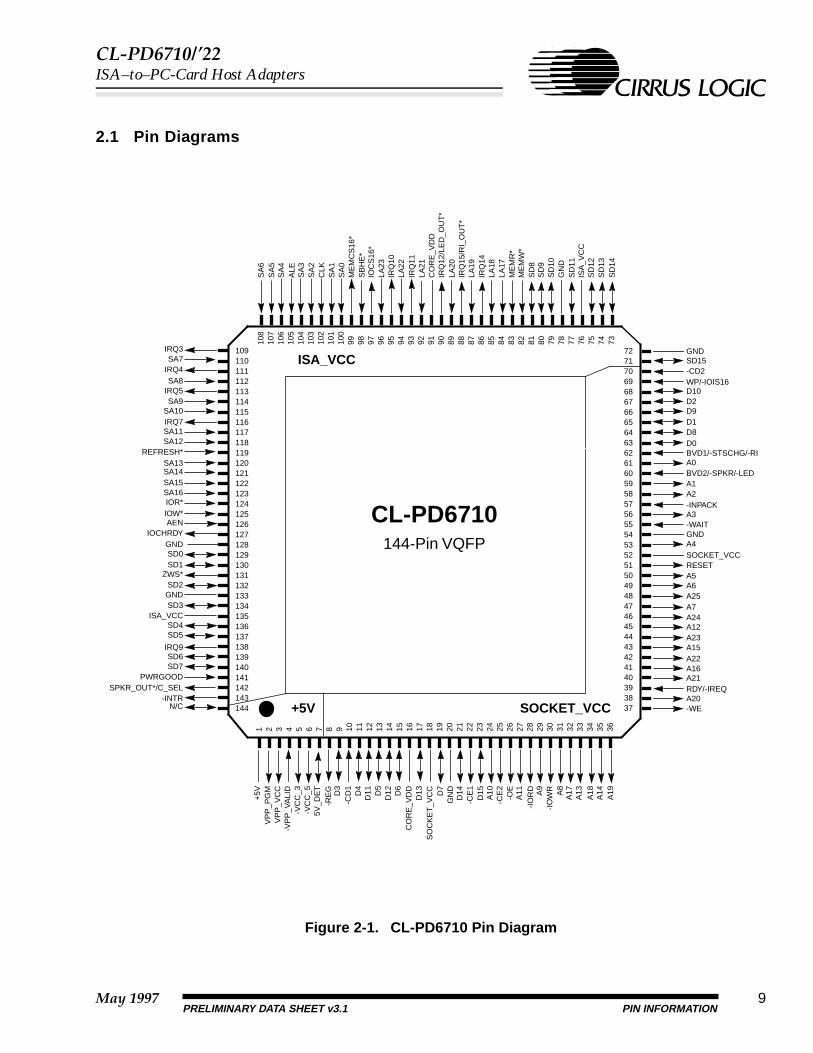
Table 2-2. Socket Interface Pins
Pin Name1 Description2
Pin NumberQty
.I/O Pwr. Drive
CL-PD6710CL-PD6722
Socket A Socket B
-REG Register Access: In Memory CardInterface mode, this output choosesbetween attribute and common mem-ory. In I/O Card Interface mode fornon-DMA transfers, this signal is active(low).
For DMA cycles on the CL-PD6722 toa DMA-capable card, -REG is inactiveduring I/O cycles to indicate a DMAcycle to or from the PC Card.
In ATA mode, this signal is alwaysinactive.
8 8 71
1 O-TS 2 or 3 2 mA
A[25:0] PC Card socket address outputs. 48, 46, 44, 42, 40, 38, 36, 34, 32, 41, 43, 35, 33, 45, 27, 24, 29, 31, 47, 49, 50, 53, 56, 58, 59, 61
48, 46, 44, 42, 40, 38, 36, 34, 32, 41, 43, 35, 33, 45, 25, 21, 28, 30, 47, 49, 50, 53, 55, 57, 58, 60
110, 108, 106, 104, 102, 100, 98, 96, 94, 103, 105, 97, 95, 107, 89, 85, 91, 93, 109, 112, 113, 115, 118, 120, 121, 123
26 O-TS 2 or 3 2 mA
D[15:0] † PC Card socket data I/O signals. 23, 21, 17, 14, 12, 68, 66, 64, 19, 15, 13, 11, 9, 67, 65, 63
20, 18, 16, 14, 12, 67, 65, 63, 17, 15, 13, 11, 9, 66, 64, 62
84, 82, 80, 77, 75, 130, 128, 126, 81, 78, 76, 74, 72, 129, 127, 125
16 I/O 2 or 3 2 mA
-OE Output Enable: For non-DMA trans-fers, this output goes active (low) toindicate a memory read from thesocket.
During a DMA write (when -IORD isactive) this output goes low if the ISAoutput TC is active (high), indicating tothe card that the system’s terminalcount signal is active. During DMAreads (when -IOWR is active), this out-put remains high.
26 23 87
1 O-TS 2 or 3 2 mA
1 To differentiate the sockets, all CL-PD6722 pin names have either A_ or B_ prepended to the pin names indicated. For example, A_A[25:0] and B_A[25:0] are the independent address buses to the sockets.
2 When a socket is configured as an ATA drive interface, socket interface pin functions change. See Table 11-1 on page 75.
PRELIMINARY DATA SHEET v3.1May 199716
PIN INFORMATION
CL-PD6710/’22ISA–to–PC-Card Host Adapters
-WE Write Enable: For non-DMA transfers,this signal goes active (low) to indicatea memory write to the socket.
During a DMA read (when -IOWR isactive), this signal goes low if the ISAoutput TC is active (high), indicating tothe card that the system’s terminalcount signal is active. During DMAwrites (when -IORD is active), this out-put remains high.
37 37 99
1 O-TS 2 or 3 2 mA
-IORD I/O Read: This output is driven low forI/O reads from the socket.
28 26 90 1 O-TS 2 or 3 2 mA
-IOWR I/O Write: This output is driven low forI/O writes to the socket.
30 29 92 1 O-TS 2 or 3 2 mA
WP/-IOIS16 †
Write Protect / I/O Is 16-Bit: In Mem-ory Card Interface mode (Interrupt andGeneral Control register, bit 5 is equalto ‘0’), this input is the status of the PCcard write protect switch.
In I/O Card Interface mode, a low onth is input ind icates that the I /Oaddress being accessed is capable of16-bit operation.
In DMA mode, this pin can be pro-grammed as the -DREQ input from aDMA-capable PC Card.
69 68 131
1 I-PU 2 or 3 –
-INPACK † Input Acknowledge: This input indi-cates to the CL-PD67XX that the PCCard supports I/O access at the cur-rent address. A PC Card activates thisinput during IORD cycles to which thecard can respond.
In DMA mode, this pin can be pro-grammed as the -DREQ input from aDMA-capable PC Card.
57 56 119
1 I-PU 2 or 3 –
RDY/-IREQ †
Ready / Interrupt Request: In Mem-ory Card Interface mode, this input isreadable as the status of bit 5 of theInterface Status register, which isused by a PC Card to signal systemsoftware of its ready or busy state.
In I/O Card Interface mode, this active-low input ind icates an in ter ruptrequest.
39 39 101
1 I-PU 2 or 3 –
Table 2-2. Socket Interface Pins (cont.)
Pin Name1 Description2
Pin NumberQty
.I/O Pwr. Drive
CL-PD6710CL-PD6722
Socket A Socket B
1 To differentiate the sockets, all CL-PD6722 pin names have either A_ or B_ prepended to the pin names indicated. For example, A_A[25:0] and B_A[25:0] are the independent address buses to the sockets.
2 When a socket is configured as an ATA drive interface, socket interface pin functions change. See Table 11-1 on page 75.
May 1997 17PRELIMINARY DATA SHEET v3.1 PIN INFORMATION

CL-PD6710/’22ISA–to–PC-Card Host Adapters
-WAIT † Wait : This input indicates to theCL-PD67XX that the current cardaccess cycle is to be extended untilthis signal becomes inactive (high).
55 54 116
1 I-PU 2 or 3 –
-CD[2:1] Card Detect: These inputs indicate tothe CL-PD67XX the presence of acard in the socket. They are pulledhigh internally in the chip.
70, 10 69, 10 132, 73
2 I-PU 1 –
-CE[2:1] Card Enable : These outputs aredriven low by the CL-PD67XX duringcard access cyc les to con t ro lbyte/word card access. -CE1 enableseven-numbered address bytes and-CE2 enables odd-numbered addressbytes. When configured for 8-bit cards,only -CE1 will be active and A0 will beset to ‘1’ for odd-byte accesses.
25, 22 22, 19 86, 83
2 O-TS 2 or 3 2 mA
RESET Reset: This output will be high to resetthe card and low for normal operation. Toreduce power consumption of idle cardsand to prevent reset glitches to a card,this signal is high-impedance unless acard is fully seated in the socket andcard interface signals are enabled.
51 51 114
1 O-TS 2 or 3 2 mA
BVD2/-SPKR/-LED †
Battery Voltage Detect 2 / Speaker /LED: In Memory Card Interface mode,this input serves as the BVD2 or bat-tery warning status input.
In I/O Card Interface mode, this inputcan be configured as a card’s -SPKRbinary audio input. For disk-drive sup-port, BVD2/-SPKR/-LED can also beconfigured as a drive-status LED input.
In DMA mode, this pin can be pro-grammed as the -DREQ input from aDMA-capable PC Card.
60 59 122
1 I-PU 2 or 3 –
Table 2-2. Socket Interface Pins (cont.)
Pin Name1 Description2
Pin NumberQty
.I/O Pwr. Drive
CL-PD6710CL-PD6722
Socket A Socket B
1 To differentiate the sockets, all CL-PD6722 pin names have either A_ or B_ prepended to the pin names indicated. For example, A_A[25:0] and B_A[25:0] are the independent address buses to the sockets.
2 When a socket is configured as an ATA drive interface, socket interface pin functions change. See Table 11-1 on page 75.
PRELIMINARY DATA SHEET v3.1May 199718
PIN INFORMATION

CL-PD6710/’22ISA–to–PC-Card Host Adapters
a General-purpose strobe controlled by ‘Socket A’ (index 2Eh/2Fh) Extension Control 2 register at extended index 0Bh.b General-purpose strobe controlled by ‘Socket B’ (index 6Eh/6Fh) Extension Control 2 register at extended index 0Bh.
BVD1/-STSCHG/-RI †
Battery Voltage Detect 1 / StatusChange / Ring Indicate: In MemoryCard Interface mode, this input servesas BVD1 (Battery Dead Status) input.
In I/O Card Interface mode, this inputis the -STSCHG input, which indicatesto the CL-PD67XX that the card’sinternal status has changed. In I/OCard Interface mode, this input canalternately be used as -RI ring indicatewhen IRQ15/RI_OUT* is configuredfor RI Out (see page 62).
62 61 124
1 I-PU 2 or 3 –
SOCKET_VCC
Connect these pins to the VCC supplyof the socket (pins 17 and 51 of therespective PC Card socket). Thesepins can thus be 0, 3.3, or 5 V, depend-ing on card presence, card type, andsystem configuration. The socket inter-face outputs ( l isted in this table,Table 2-2) will operate at the voltageapplied to these pins, independent ofthe vo l tage app l ied to o therCL-PD67XX pin groups.
18, 52 24, 52 88, 117
2 PWR – –
Table 2-3. General-Purpose Strobe / Voltage Sense Pins
Pin Name Description
Pin NumberQty
.I/O Pwr. Drive
CL-PD6710CL-PD6722
Socket A Socket B
GPSTB General-Purpose Strobe: ConnectA_GPSTB to pin 43 and B_GPSTB topin 57 on PC Card socket. This pin canbe used with external logic to sensepins VS1 and VS2 of the socket. It isonly available on the CL-PD6722.a, b
– 6 7
1 I-PU/O-OC 1 2 mA
5V_DET This status input is used to detect5 V/3.3 V on PCMCIA pin 57.
7 – – 1 I-PU 1 N/A
Table 2-2. Socket Interface Pins (cont.)
Pin Name1 Description2
Pin NumberQty
.I/O Pwr. Drive
CL-PD6710CL-PD6722
Socket A Socket B
1 To differentiate the sockets, all CL-PD6722 pin names have either A_ or B_ prepended to the pin names indicated. For example, A_A[25:0] and B_A[25:0] are the independent address buses to the sockets.
2 When a socket is configured as an ATA drive interface, socket interface pin functions change. See Table 11-1 on page 75.
May 1997 19PRELIMINARY DATA SHEET v3.1 PIN INFORMATION

CL-PD6710/’22ISA–to–PC-Card Host Adapters
Table 2-4. Power Control Pins
Pin Name Description
Pin NumberQty
.I/O Pwr. Drive
CL-PD6710CL-PD6722
Socket A Socket B
VPP_VCC This output is used to enable thesocket VCC supply onto the VPP pin.This pin is mutually exclusive withVPP_PGM.
3 2 205
1 O 1 12 mA
VPP_PGM This output is used to enable the pro-gramming voltage supply onto the VPPpin. This pin is mutually exclusive withVPP_VCC.
2 1 204
1 O 1 12 mA
-VCC_3 This output is used to enable a 3.3Vsupply onto the VDD socket. This pin ismutually exclusive with -VCC_5.
5 4 2061 O 1 12
mA
-VCC_5 This output is used to enable a 5V sup-ply onto the VDD socket. This pin ismutually exclusive with -VCC_3.
6 5 2071 O 1 12
mA
Table 2-5. Power and Ground Pins
Pin Name DescriptionPin Number
Qty. I/O Pwr. DriveCL-PD6710 CL-PD6722
+5V This pin is connected to the system’s 5-voltpower supply. In systems where 5 volts is notavailable, this pin can be connected to thesystem’s 3.3-volt supply (but 5-volt-only PCCards will not be supported).
1 208
1 PWR – –
CORE_VDD This pin provides power to the core circuitry ofthe CL-PD67XX. It can be connected to eithera 3.3- or 5-volt power supply, independent ofthe operating voltage of other interfaces. Forpower conservation on a system with a 3.3-volt supply available, this pin should be con-nected to the 3.3-volt supply even if there is nointention of operating other interfaces on thedevice at less than 5 volts.
16, 91 27, 133
2 PWR – –
GND All ground pins should be connected to sys-tem ground.
20, 54, 72, 78, 128, 133
31, 70, 79, 111, 140, 192 6 GND – –
PRELIMINARY DATA SHEET v3.1May 199720
PIN INFORMATION

CL-PD6710/’22ISA–to–PC-Card Host Adapters
Table 2-6 below summarizes the pin usage.
2.4 Power-On Configuration Summary
On the rising edge of PWRGOOD, the CL-PD67XX latches the configuration pin SPKR_OUT*/C_SEL todetermine which sockets are addressed by this device. A ‘1’ on the SPKR_OUT*/C_SEL pin will causethe device to address Socket 0 (and Socket 1 for the CL-PD6722). A ‘0’ on this pin will cause the deviceto address Socket 2 (and Socket 3 for the CL-PD6722).
Table 2-6. Pin Usage Summary
Pin GroupPin Quantity
CL-PD6710 CL-PD6722
ISA bus interface pins 69 69
Socket interface pins 60 120
General-purpose strobe pins 0 2
Voltage sense pins 1 0
N/C 1 0
Power control pins 4 8
Power and ground pins 9 9
Total: 144 208
Table 2-7. Chip Configuration at Power-up for Socket Support
SPKR_OUT*/C_SEL Level at Rising
Edge of PWRGOOD
CL-PD6710 CL-PD6722
Socket Interface SupportSocket A
Interface SupportSocket B
Interface Support
High PC Card Socket 03E0 Index 00h–3Fh
PC Card Socket 03E0 Index 00h–3Fh
PC Card Socket 13E0 Index 40h–7Fh
Low PC Card Socket 23E0 Index 80h–BFh
PC Card Socket 23E0 Index 80h–BFh
PC Card Socket 33E0 Index C0h–FFh
May 1997 21PRELIMINARY DATA SHEET v3.1 PIN INFORMATION

CL-PD6710/’22ISA–to–PC-Card Host Adapters
3. INTRODUCTION
3.1 System Architecture
This section describes PC Card basics, windowing,interrupts, CL-PD67XX power management, socketpower management, write FIFO, bus sizing, pro-grammable PC Card timing, and ATA and DMAmode operation.
3.1.1 PC Card Basics
PCMCIA is an abbreviation for Personal ComputerMemory Card International Association. PC CardStandard1 is a standard for using memory and I/Odevices as insertable, exchangeable peripherals forPCs (personal computers) and handheld comput-ers. For simpler end-user and vendor implementa-tion of the standard, systems employing PC CardStandard should also be backward-compatible withindustry-standard PC addressing.
The memory information for memory-type PC Cardsmust be mapped into the system memory addressspace. This is accomplished with a ‘windowing’ tech-nique that is similar to expanded memory schemesalready used in PC systems (for example, LIM 4.0memory manager).
PC Cards can have attribute and common memory.Attribute memory is used to indicate to host softwarethe capabilities of the PC Card, and it allows hostsoftware to change the configuration of the card.Common memory can be used by host software forany purpose (such as flash file system, systemmemory, and floppy emulation).
1 The CL-PD67XX is backward-compatible with PCMCIA standards 1.0, 2.0, 2.01, and 2.1. The CL-PD67XX is also compatible with JEIDA 4.1 and its earlier standards corresponding with the PCMCIA standards above.
22INTRODUCTION
I/O-type PC Cards, such as modems, should alsobe directly addressable, as if the cards were I/Odevices plugged into the ISA bus. For example, itwould be highly desirable to have a PC Card modemaccessible to standard communications software asif it were at a COM port. For COM1, this wouldrequire that the modem be accessed at system I/Oaddress 3F8h–3FFh. The method of mapping a PCCard I/O address into anticipated areas of ISA I/Ospace is done similarly to memory windowing.
I/O-type PC Cards usually have interrupts that needto be serviced by host software. For the example ofa modem card accessed as if at COM1, softwarewould expect the modem to generate interrupts onthe IRQ4 line. To be sure all interrupts are routed asexpected, the CL-PD67XX can steer the interruptfrom the PC Card to one of several standard PCinterrupts (see Section 3.1.4 and the Interrupt andGeneral Control register on page 42).
3.1.2 CL-PD67XX Windowing Capabilities
For full compatibility with existing software, and toensure compatibility with future memory cards andsoftware, the CL-PD67XX provides five program-mable memory windows per socket and two pro-grammable I/O windows per socket. These windowscan be used by an inserted PC Card to access ISAmemory and I/O space.
Having five memory windows per socket allows amemory-type card to be accessed through fourmemory windows programmed for common mem-ory access (allowing PC-type expanded-memory-style management), leaving the fifth memory win-dow available to be programmed to access thecard’s attribute memory without disrupting the com-mon memory in use.
PRELIMINARY DATA SHEET v3.1May 1997

CL-PD6710/’22ISA–to–PC-Card Host Adapters
Each of the five memory windows has several programming options, including:
Each of the two I/O windows has several programming options, including:
CAUTION: The windows of the CL-PD67XX should never be allowed to overlap with each other or the other devicesin the system. This would cause collisions in the IOCS16*, MEMCS16*, IOCHRDY, and SD[15:0] sig-nals, resulting in erratic behavior.
Memory Window Option
Description
Enabled Each of the five memory windows can be individually enabled. Disabled windows are not respondedto.
Start Address The starting address of the window is programmable on 4-Kbyte boundaries starting at 64 Kbytes(1000h) with a maximum address of 16 Mbyte.
End AddressThe ending address of the window is programmable on 4-Kbyte boundaries starting at 64 Kbytes(1000h) with a maximum address of 16 Mbyte. Only memory accesses between the starting andending address are responded to.
Offset Address The offset address is added to the ISA address to determine the address for accessing the PC Card.This allows the addresses in the PC Card address space to be different from the ISA address space.
Data Size The size of accesses can be set manually to either 8 or 16 bits.
Timing The timing of accesses (Setup/Command/Recovery) can be set by either of two timing register sets:Timer Set 0 or Timer Set 1.
Register Access Setting
The -REG pin can be enabled on a per-window basis so that any of the windows can be used foraccessing attribute memory.
Write Protect If the window is programmed to be write-protected, then writes to the memory window are ignored(reads are still performed normally).
I/O Window Option
Description
Enabled Each of the two I/O windows can be individually enabled.
Start Address The starting address of the window is programmable on single-byte boundaries from 0 to 64 Kbytes.
End Address The ending address of the window is also programmable on single-byte boundaries from 0 to 64Kbytes.
Offset Address The offset address is added to the ISA address to determine the address for accessing the PC Card.
Auto Size The size of accesses can be set automatically, based on the PC Card -IOIS16 signal.
Data Size The size of accesses can be set manually to either 8 or 16 bits, overriding the Auto Size option.
Timing The timing of accesses (Setup/Command/Recovery) can be set by either of two timing register sets:Timer Set 0 or Timer Set 1.
May 1997 23PRELIMINARY DATA SHEET v3.1 INTRODUCTION

CL-PD6710/’22ISA–to–PC-Card Host Adapters
Figure 3-1. Memory Window Organization
Figure 3-2. I/O Window Organization
ISA Memory Address Space
PC Card Memory Address Space
Common Memory
AttributeMemory
Card Memory Map
System Memory Map
System Memory MapEnd Address Registers
Start Address Registers
Offset Address Registers
Card Memory Window
Memory Window
16 Mbytes
64 Mbytes
NOTE: ISA memory window can map to eithercommon or attribute PC Card memory.
First 64 Kbytes
not usable inmost ISA systems
ISA I/O Address Space
PC Card I/O Address Space
System I/O Map
System I/O MapEnd Address Registers
Start Address Registers
I/O Window
Card I/O Window
64 Mbytes
64 Kbytes
Card I/O Map Offset Address Registers
PRELIMINARY DATA SHEET v3.1May 199724
INTRODUCTION

CL-PD6710/’22ISA–to–PC-Card Host Adapters
3.1.3 CL-PD67XX Functional Blocks
Figure 3-3. Functional Block Diagram
OperationRegisters
Mapperand
Offset
Socket
Socket
WriteFIFO
Power Control
InterruptControl
Synthe-
BusInterface
Unit
sizer
Per Chip Per Socket
Control
Data
Address
VCC ControlVPP Control
ControlAddress
Data
Clock
INTR
IRQs
Bus Control
Timing Control
-WAIT
WP/-IOIS16
CD1, CD2
RDY/-IREQBVD, -STSCHG
3.1.4 Interrupts
The CL-PD67XX provides ten interrupt pins that arelabeled with names suggesting their mapping in thesystem, though there are no hard requirementsspecifying the exact mapping. Typically, all ten inter-rupt pins should be connected to system interruptsignals to allow maximum flexibility in programminginterrupt routing from the CL-PD67XX.
Classes of Interrupts
The CL-PD67XX supports two classes of interrupts:
● Socket or card interrupts initiated by the PC Cardactivating its RDY/-IREQ signal
● Management interrupts triggered by changes inPC Card status, including:
— Card insertion or removal
— Battery warning indicator (BVD2) change ona memory-type card
— Battery dead indicator (BVD1) or I/O-typecard status change (-STSCHG)
— Ready (RDY) status change on a memory-type card
Either class of interrupts can be routed to any of theten interrupt pins on the CL-PD67XX.
Connection of Interrupt Pins
IRQ interrupts in PC-compatible systems are notgenerally shared by hardware. Therefore, eachdevice in the system using IRQ interrupts must havea unique interrupt line. Additionally, many softwareapplications assume that certain I/O devices usespecific IRQ signals. To allow PC Cards with differ-ing I/O functionalities to be connected to appropriatenonconflicting IRQ locations, the CL-PD67XX cansteer the interrupt signal from a PC Card to any oneof the ten different hardware interrupt lines.
For some I/O-type cards, software is written so thatIRQ interrupts can be shared. The CL-PD67XX con-tains unique logic that allows IRQ interrupts to beshared under software control. This is accomplishedby programming the CL-PD67XX to alternatelypulse and then three-state the desired interrupt pin,which has been programmed as an IRQ output. Thisunique IRQ interrupt sharing technique can be con-trolled through software so that systems incapableof IRQ sharing have no loss of functionality.
May 1997 25PRELIMINARY DATA SHEET v3.1 INTRODUCTION

CL-PD6710/’22ISA–to–PC-Card Host Adapters
3.1.5 Alternate Functions of Interrupt Pins
The CL-PD67XX has two interrupt pins that can beprogrammed fo r a l te r na te func t ions :IRQ12/LED_OUT* and IRQ15/RI_OUT*. In addi-tion, the CL-PD6722 allows IRQ9 and IRQ10 to beprogrammed for system DMA transfer handshakefunctions.
3.1.5.1 IRQ12 as LED_OUT* Driver
If a disk-activity or card-cycle-activity indicator isdesired, IRQ12/LED_OUT* can be programmedas an open-collector LED driver, capable of drivingmost common LEDs. There is no specific bit thatprograms the IRQ12 pin to become an LED driver;instead, whenever a socket interface is pro-grammed to support a drive status LED input or isprogrammed to show card activity on the LED (asdescribed below), the IRQ12 pin becomes recon-figured as an open-collector LED driver.
The Extension Control 1 register’s LED ActivityEnable bit (extended index 03h bit 2) is used toenable the LED being used to show card activity.When this bit is set, any type of read or write cyclesto the respec t i ve socke t cause theIRQ12/LED_OUT* signal to be driven low for theduration of the card activity.
The Drive LED Enable bit (Misc Control 2 registerbit 4) is used to enable the BVD2/-SPKR/-LEDinput from an I/O-interfaced card to be interpretedas a drive LED input, where an open-collector sig-nal driven low on this input wil l cause theIRQ12/LED_OUT* open-collector output to go low.
Any combination of settings of LED Activity Enableand Drive LED Enable bits can be used on eachsocket, with each type of activity being able to sep-arately cause the LED to be illuminated. Statusfrom non-present or non-activated cards is auto-mat i ca l l y masked o f f f rom caus ing theIRQ12/LED_OUT* signal to be driven low.
3.1.5.2 IRQ15 as RI_OUT*
If the capability to ‘wake up’ a system on an incom-ing phone call to a PC Card modem is desired, itmay be necessary in some systems to use a dedi-cated wakeup signal to the system’s SMI or NMIcontroller to facilitate this instead of using the nor-mal interrupt connections. If this is the case, the
IRQ15 connection can be reprogrammed to passthrough a qualified version of an I/O interfacedcard’s -RI signal.
IRQ15/RI_OUT* is programmed as RI_OUT* byprogramming the IRQ15 Is RI Out bit (Misc Con-trol 2 register 1Eh bit 7) to ‘1’. Then if a particularsocket suppor t ing a modem is to have i tsBVD1/ -STSCHG/-RI p in passed to theIRQ15/RI_OUT* pin, that socket’s Ring IndicateEnable bit (Interrupt and General Control regis-ter 03h bit 7) should be set to ‘1’.
When the CL-PD67XX is configured this way, a lowlevel at the BVD1/-STSCHG/-RI pin on an I/O inter-faced PC Card will cause the IRQ15/RI_OUT* sig-nal to become active-low (because it is intended tobe connected to an SMI* or NMI* input on the sys-tem processor or core logic). To prevent multipleSMI or NMI interrupts from occurring on one ringcondition, the IRQ15/RI_OUT* pin remains lowuntil ISA bus activity resumes, indicated by theresumption of ISA bus memory or I/O reads orwrites.
3.1.5.3 IRQ9 as DACK* and IRQ10 as DRQ
When a CL-PD6722 is to be used for DMA sup-port, IRQ9 is programmed as a DACK* input froman ISA bus DACK* signal selected by the systemdesigner. Similarly, IRQ10 is programmed as anactive-high DRQ output to the ISA bus and shouldbe connected to the system bus DRQ signal corre-sponding to that used for DACK*.
IRQ9 and IRQ10 are thus redefined for DMA cyclesupport by the setting of the DMA System bit (MiscControl 2 register 1Eh, bit 6) to ‘1’. Setting theDMA System bit redefines these ISA interface sig-nals but does not cause DMA to a card to beenabled.
3.1.6 General-Purpose Strobe Feature
The CL-PD6722 has capability to use two pins asgeneral-purpose strobes. This is a feature thatcauses a pin programmed as a general-purposestrobe to appear in software as an extended regis-ter in the CL-PD6722 register set, while in realityaccesses to this extended register cause the gen-eral-purpose strobe pin to go active during the reg-ister access. The strobe can be programmed to
PRELIMINARY DATA SHEET v3.1May 199726
INTRODUCTION

CL-PD6710/’22ISA–to–PC-Card Host Adapters
activate on reads or writes to this virtual extendedregister, allowing straightforward single-chip imple-mentation of an 8-bit general purpose read or writeport.
Chapter 12 provides detailed information on howthis port can be used.
3.1.7 Voltage Sense Pins
The CL-PD6710 provides a single pin to detect 5 Vor 3.3 V on pin 57 of the PC Card.
The CL-PD6722 can be simply configured for dual-socket VS1 and VS2 detection with an externalread port consisting of half of a ’244 buffer or othersimilar device, enabled by the B_GPSTB pin pro-grammed as a read port.
Chapter 13 provides detailed information on theprogramming model for VS1 and VS2 detectionand how connections are made to achieve thisfunctionality.
3.1.8 CL-PD67XX Power Management
To provide the longest possible battery life, theCL-PD67XX provides many power managementfeatures, including Low-Power Dynamic mode, Sus-pend mode, and control of PC Card socket power.
Low-Power Dynamic mode is transparent to the ISAbus. After reset, the CL-PD67XX is configured forLow-Power Dynamic mode. This mode can beturned off by setting Misc Control 2 register, bit 1 to‘0’. When in Low-Power Dynamic mode, periods ofinactivity (no activity on the PC Card bus and systemaccesses to chip registers or inserted cards are nolonger being performed) cause the CL-PD67XX toenter a low-power state where the clock is turned offto most of the chip and the PC Card address anddata lines are set to a static value. VCC and VPPpower to the card is left unchanged. When there isactivity present on the PC Card bus, or the systemaccesses CL-PD67XX registers, or PC Cards areinserted or removed from the socket, theCL-PD67XX enters its active state, services thetransaction, and then returns to its low-power state.
A Suspend mode can also be programmed. TheCL-PD67XX Suspend mode is the chip’s lowestsoftware-controlled power mode. The CL-PD67XXis put into Suspend mode by setting the Misc Con-
trol 2 register, bit 2 to ‘1’. In Suspend mode, all theinternal clocks are turned off, and only read/writeaccess to the Index register and write access to theMisc Control 2 register is supported. All accessesto the PC Cards are ignored when in Suspendmode. VCC and VPP power to the card is leftunchanged (the system power management soft-ware is responsible for turning off power to thesocket and entering Suspend mode). Interrupts andring indicate signals are passed through to the sys-tem bus when in Suspend mode. To exit Suspendmode, the Misc Control 2 register bit 2 must bereset to ‘0’. It requires 50 ms for the CL-PD67XX torestart the internal clock synthesizer and becomeactive again.
In addition to the software suspend, if the systemhold’s the AEN signal of the CL-PD67XX high, ahardware-assisted Super-Suspend mode occurswhere ISA inputs to the chip are internally shut off.Internal in the CL-PD67XX, the ISA inputs areignored and floating conditions on the ISA bus willnot cause high current flow in the CL-PD67XX ISAinput receivers. Since the ISA bus inputs to the corelogic of the CL-PD67XX are also not toggling whenAEN is set high, power consumption is furtherreduced. Interrupts and ring indicate signals arepassed through to the system bus when in Super-Suspend mode
The CL-PD67XX power can be further managed bycontrolling socket power as outlined in Section3.1.9. Socket power can be turned on and offthrough software or automatically when cards areinserted or removed. The CL-PD67XX provides sixpins per socket for controlling external logic to switchVCC and VPP voltages on and off and for sensing acard’s operating voltage range. Cards can be turnedoff when not in use.
May 1997 27PRELIMINARY DATA SHEET v3.1 INTRODUCTION

CL-PD6710/’22ISA–to–PC-Card Host Adapters
a IOR*, IOW*, MEMR*, and MEMW* must be held high when PWRGOOD is low to prevent manufacturing test mode outputs from driving the system data bus.
Table 3-1. CL-PD67XX Power-Management Modes
Mode NamePWRGOOD
LevelAEN
Misc Control 2 Register
Functionality
Typical Power Consumption(CORE_VDD =
3.3 V, ISA_VCC,
SOCKET_VCC, and +5V = 5.0 V)
SuspendMode(Bit 2)
Low-Power Dynamic
Mode(Bit 1)
Low-Power Dynamic (Default)
High Normal 0 1 Full functionality< 45 mW high activity, 9–14 mW normal system activity
Normal High Normal 0 0 Full functionality< 85 mW high activity, 18 mW normal sys-tem activity
Suspend(Software
Controlled)High Normal 1 –
8-bit access to Misc Control 2 register. No other register access. No card in socket(s).
< 2 mW
Super-Suspend(Hardware Controlled)
High Static High 1 –
No register access. No card in socket(s). System bus signals disabled (clock off).
< 1 mW
Reset Lowa – – –
No register access. No card in socket(s). System bus signals disabled.
9–14 mW
3.1.9 Socket Power Management Features
Card Removal
When a card is removed from a socket, theCL-PD67XX by default automatically disables theVCC and VPP supplies to the socket. If ExtensionControl 1 register bit 1 is ‘0’, card power is pre-vented from being automatically disabled when acard is removed. The CL-PD67XX can also be con-figured to have management interrupts notify soft-ware of card removal.
Card Insertion
Power to the socket is off at reset and wheneverthere is no card in a socket. When a card is detected(card detect input pins, -CD1 and -CD2, to theCL-PD67XX become asserted low), two indepen-dent actions can be programmed to occur.
If the CL-PD67XX has been set for automaticpower-on (Power Control register bits 4 and 5 areboth ‘1’), the CL-PD67XX automatically enables thesocket VCC supply (and, if so programmed, the VPPsupply).
If the CL-PD67XX has been programmed to causemanagement interrupts for card-detection events,assertion of -CD1 and -CD2 to the CL-PD67XXcauses a management interrupt to inform systemsoftware that a card was inserted. In the case ofmanual power detection (Power Control register bit5 is ‘0’), system software can determine the card’soperating voltage range and then power-up thesocket and initialize the card (or simply initialize thecard if programmed for automatic power-on (PowerControl register bit 5 is ‘1’ and Extension Control1 register bit 1 is ‘1’)).
PRELIMINARY DATA SHEET v3.1May 199728
INTRODUCTION

CL-PD6710/’22ISA–to–PC-Card Host Adapters
3.1.10 Write FIFO
To increase performance when writing to PC Cards,two, independent, four-word-deep write FIFOs areused. Writes to PC Cards will complete without waitstates until the FIFO is full. Register states shouldnot be changed until the write FIFO is empty.
3.1.11 Bus Sizing
The CL-PD67XX incorporates logic to automaticallydetect its connection to 8- or 16-bit buses. This isaccomplished by sensing SBHE* input activity. If theSBHE* pin is always high (that is, tied to ISA_VCC),the CL-PD67XX operates in 8-bit mode where alltransfers occur on the lower data bus, bits 7:0. Anyoccurrence of the SBHE* going low triggers theCL-PD67XX to operate thereafter as a 16-bit device.16-bit operation of the CL-PD67XX is properly trig-gered when the SBHE* input is connected to thesystem’s SBHE* signal. When the CL-PD67XX isoperating in 16-bit mode, all ISA bus transactionsare 16-bit whenever possible, even if installed PCcards only support 8-bit transfers. In 16-bit mode,the signals SBHE* and SA0 are used to specify thewidth of the data transfer and the location of data onthe bus (which byte lane has the data) during 8-bittransfers. The possible combinations for SBHE* andSA0 are shown in Table 3-2 and Table 3-3.
a The SBHE* signal is pulled up. If the SBHE* signal remains high, the CL-PD67XX causes all transfers to occur on D[7:0] only.
Typically, there are three types of data transfers toand from the CL-PD67XX:
● 16-Bit Transfer from 16-Bit Processor — TheCPU puts the address on the bus. Then theCL-PD67XX identifies the address on the bus aseither an 8- or 16-bit transfer. If the transfer isidentified as 16-bit, the host acknowledges withthe appropriate signal, either MEMCS16* orIOCS16*. Data is transferred to/from the databus as a word on both byte lanes.
● 8-Bit Transfer from 16-Bit Processor — TheCPU puts the address on the bus. Then theCL-PD67XX identifies the address on the bus aseither an 8- or 16-bit transfer. In this case, thetransfer is identified as an 8-bit transfer. The hostqueries SA0 and SBHE* to determine the bytelane on which the transfer is to occur. The data istransferred to/from the data bus (see Table 3-2).
● 8-Bit Transfer from 8-Bit Processor — TheCPU puts the address on the bus. The hostdetermines that it will be an 8-bit transfer sincethe SBHE* signal has been tied high. TheCL-PD67XX queries SA0 to determine if the byteis odd/even. The data is transferred to/from theData bus (D[7:0]).
3.1.12 Programmable PC Card Timing
The Setup, Command, and Recovery time for thePC Card bus is programmable (see Chapter 10).The CL-PD67XX can be programmed to match thetiming requirements of any PC Card. There are twosets of timing registers, Timer Set 0 and Timer Set 1,that can be selected on a per-window basis for bothI/O and memory windows.
To be compatible with the 82365SL, the two timingsets are programmed at the r ising edge ofPWRGOOD to include normal-wait and one-wait-state timing.
3.1.13 ATA Mode Operation
The CL-PD67XX supports direct connection toAT-attached-interface hard drives. ATA drives usean interface very similar to the IDE interface foundon many popular portable computers. In this mode,the address and data conflict with the floppy drive ishandled automatically. See Chapter 11 for moreinformation.
Table 3-2. 16-Bit Mode Operation
16-Bit Mode Transfer Types SBHE* SA0
Word 0 0
Upper Byte/Odd Address 0 1
Low Byte/Even Address 1 0
Not Valid 1 1
Table 3-3. 8-Bit Mode Operation
8-Bit Mode Transfer Typesa SA0
Even Address 0
Odd Address 1
May 1997 29PRELIMINARY DATA SHEET v3.1 INTRODUCTION
CL-PD6710/’22ISA–to–PC-Card Host Adapters
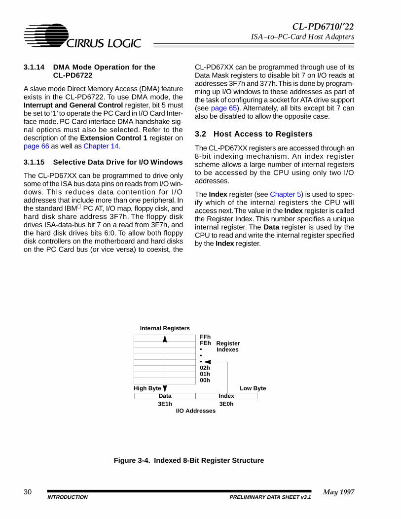
3.1.14 DMA Mode Operation for the CL-PD6722
A slave mode Direct Memory Access (DMA) featureexists in the CL-PD6722. To use DMA mode, theInterrupt and General Control register, bit 5 mustbe set to ‘1’ to operate the PC Card in I/O Card Inter-face mode. PC Card interface DMA handshake sig-nal options must also be selected. Refer to thedescription of the Extension Control 1 register onpage 66 as well as Chapter 14.
3.1.15 Selective Data Drive for I/O Windows
The CL-PD67XX can be programmed to drive onlysome of the ISA bus data pins on reads from I/O win-dows. This reduces data contention for I/Oaddresses that include more than one peripheral. Inthe standard IBM PC AT, I/O map, floppy disk, andhard disk share address 3F7h. The floppy diskdrives ISA-data-bus bit 7 on a read from 3F7h, andthe hard disk drives bits 6:0. To allow both floppydisk controllers on the motherboard and hard diskson the PC Card bus (or vice versa) to coexist, the
CL-PD67XX can be programmed through use of itsData Mask registers to disable bit 7 on I/O reads ataddresses 3F7h and 377h. This is done by program-ming up I/O windows to these addresses as part ofthe task of configuring a socket for ATA drive support(see page 65). Alternately, all bits except bit 7 canalso be disabled to allow the opposite case.
3.2 Host Access to Registers
The CL-PD67XX registers are accessed through an8-bit indexing mechanism. An index registerscheme allows a large number of internal registersto be accessed by the CPU using only two I/Oaddresses.
The Index register (see Chapter 5) is used to spec-ify which of the internal registers the CPU willaccess next. The value in the Index register is calledthe Register Index. This number specifies a uniqueinternal register. The Data register is used by theCPU to read and write the internal register specifiedby the Index register.
Figure 3-4. Indexed 8-Bit Register Structure
00h01h02h•
•FEhFFh
•
3E1h 3E0h
Internal Registers
Register Indexes
I/O Addresses
Data IndexHigh Byte Low Byte
PRELIMINARY DATA SHEET v3.1May 199730
INTRODUCTION

CL-PD6710/’22ISA–to–PC-Card Host Adapters
Figure 3-5. Indexed 8-Bit Register Example
The following code segment demon-strates use of an indexed 8-bit register:
mov dx, 3E0hmov al, 02hmov ah, 3Chout dx, ax
02h
3E1h 3E0h
Internal Registers
RegisterIndexes
I/O Addresses
3Ch 02h
3Ch
AH AL
Double-Indexed Registers
The CL-PD67XX has Extension registers that add tothe functionality of the 82365SL-compatible registerset. Within the Extension registers is an ExtendedIndex register and Extended Data register that pro-vide access to more registers. The registersaccessed through Extended Index and ExtendedData are thus double indexed. The example belowshows how to access the Extension Control 1 reg-ister, one of the double-indexed registers.
;Write to Extension Control 1 register example
;Constants sectionExtended_IndexEQU 2EhIndex_RegEQU 2FhExt_Cntrl_1EQU 03hPD67XX_IndexEQU 3E0h
;Code sectionmov dx, PD67XX_Indexmov al, Extended_Indexmov ah, Ext_Cntrl_1out dx, axmov al, Index_Regmov ah, user_data;Desired data to beout dx, ax;written to
;extended index 03h
;Read from Extension Control 1 register example
;Code sectionmov dx, PD67XX_Indexmov al, Extended_Index
May 1997PRELIMINARY DATA SHEET v3.1
mov ah, Ext_Cntrl_1out dx, axmov al, Index_Regout dx, alinc dx ;al has extendedin al, dx;index 03h data
3.3 Power-On Setup
Following reset, the CL-PD67XX must be config-ured by host software. The host software’s setupprocedure is different depending on its PC systemconfiguration, in particular, the power supplyarrangement.
The application of the RESET signal (see page 18)on power-up causes initialization of all theCL-PD67XX register bits and fields to their reset val-ues. Not all registers have reset values; only regis-ters with bits and fields specified to have resetvalues are initialized.
One bit, which is loaded on hardware reset from theSPKR_OUT*/C_SEL pin (see page 15), is used todetermine the socket to which the CL-PD67XX willrespond.
31INTRODUCTION

CL-PD6710/’22ISA–to–PC-Card Host Adapters
4. REGISTER DESCRIPTION CONVENTIONS
Register Headings
The description of each register starts with aheader containing the following information:
Special Function Bits
Following is a description of bits with special func-tions:
a When the register is socket-specific, the Index value given in the register heading is for Socket A only. For the Socket B register on the CL-PD6722, add 40h to the Index value of the Socket A register.
Bit Naming Conventions
The following keywords are used within bit andfield names:
Read/Write Convention
Header Field Description
Register Name Indicates the register name.
Index aThe Index value through which an inter-nal register in an indexed register set isaccessed.
Register Per
Indicates whether the register affectsboth sockets, marked chip, or an individ-ual socket, marked socket. If socket isindicated, there are two registers beingdescribed, each with a separate Indexvalue (one for each socket, A and B). a
Register Compatibility Type
Indicates whether the regis ter is82365SL-compatible, marked 365 or aregister extension, marked ext.
Bit Type Description
Reserved These bits are Reserved and should notbe changed.
Compatibility Bit
These bits have no function on theCL-PD67XX, but are included for com-patibility with the 82365SL register set.
0 or 1These read-only bits are forced to either‘0’ o r ‘ 1 ’ a t rese t and canno t bechanged.
Scratchpad Bit These read/write bits are available foruse as bits of memory.
Keyword Description
EnableIndicates that the function described inthe rest of the bit name is active whenthe bit is ‘1’.
DisableIndicates that the function described inthe rest of the bit name is active whenthe bit is ‘0’.
ModeIndicates that the function of the bitalters the interpretation of the values inother registers.
Input Indicates a bit or field that is read from apin.
Output Indicates a bit or field that is driven to apin.
Select
Indicates that the bit or field selectsbetween multiple alternatives. Fieldsthat contain Select in their names havean indirect mapping between the valueof the field and the effect.
Status
Indicates one of two types of bits: eitherread-only bits used by the CL-PD67XXto report information to the system, orbits set by the CL-PD67XX in responseto an event, and can also be cleared bythe system. The system cannot directlycause a Status bit to become ‘1’.
Value Indicates that the bit or field value isused as a number.
Bit Access Description
RW:n Bit is read/write and resets to value nwhen PWRGOOD is cycled.
RBit is read-only and setting is deter-mined by conditions noted. Set this bitto ‘0’, or echo back value read.
R:nBit is read-only and resets to value nwhen PWRGOOD is cycled. Set this bitto ‘0’, or echo back value read.
R:n W:mBit is read/write and resets to value nwhen PWRGOOD is cycled. Set this bitto value m only.
PRELIMINARY DATA SHEET v3.1May 199732
REGISTER DESCRIPTION CONVENTIONS

CL-PD6710/’22ISA–to–PC-Card Host Adapters
5. OPERATION REGISTERS
The CL-PD67XX internal registers are accessed through a pair of Operation registers — an Index registerand a Data register. The Index register is accessed at address 03E0h, and the Data register is accessedat 03E1h.
5.1 Index
The Data register is accessed at 03E1h.
Bits 5:0 — Register Index
These bits determine which of the 64 possible socket-specific registers will be accessed when theData register is next accessed by the processor. Note that some values of the Register Index fieldare reserved (see Table 5-1).
Bit 6 — Socket Index
This bit determines which set of socket-specific registers is currently selected. When this bit is ‘0’,a Socket A register is selected. When this bit is ‘1’, a Socket B register is selected. Note that theCL-PD6710 supports one socket, and the CL-PD6722 supports two sockets.
Bit 7 — Device Index
In systems where two CL-PD67XXs are used, this bit differentiates between them.
The Index register value determines which internal register should be accessed (read or written) inresponse to each CPU access of the Data register. Each of the possible PC Card sockets is allocated 64of the 256 locations in the internal register index space.
Figure 5-1. Device/Socket/Register Index Space
When viewed as a 8-bit value, the contents of the Index register completely specify a single internal-reg-ister byte. For example, when the value of this register is in the range 00h–3Fh, a Socket A register isselected (Socket Index bit is ‘0’), and when the value of this register is in the range 40h–7Fh, a Socket Bregister is selected (Socket Index bit is ‘1’). This register only reads back for Device 0. Device 1 will readback only the upper data byte when 16-bit reads occur at 3E0h.
Register Name: IndexIndex: n/a
Register Per: chipRegister Compatibility Type: 365
Bit 7 Bit 6 Bit 5 Bit 4 Bit 3 Bit 2 Bit 1 Bit 0
Device Index Socket Index Register Index
RW:0 RW:0 RW:000000
Socket B Registers
Socket A Registers00h
3Fh40h
80h7Fh
FFhSocket D Registers
Socket C Registers
Possible with two CL-PD67XXs
May 1997 33PRELIMINARY DATA SHEET v3.1 OPERATION REGISTERS

CL-PD6710/’22ISA–to–PC-Card Host Adapters
PRELIMINARY DATA SHEET v3.1May 199734
OPERATION REGISTERS
The internal register that is accessed when the CPU reads or writes the Data register is determined bythe current value of the Index register, as follows:
Table 5-1. Index Registers
Register NameIndex Value
ChapterPage
NumberSocket A Socket Ba
Chip Revision 00hb
Chapter 6:Chip Control
37
Interface Status 01h 41h 38
Power Control 02h 42h 40
Interrupt and General Control 03h 43h 42
Card Status Change 04h 44h 44
Management Interrupt Configuration 05h 45h 45
Mapping Enable 06h 46h 47
I/O Window Control 07h 47h
Chapter 7:I/O Window
Mapping
49
System I/O Map 0 Start Address Low 08h 48h 50
System I/O Map 0 Start Address High 09h 49h 50
System I/O Map 0 End Address Low 0Ah 4Ah 51
System I/O Map 0 End Address High 0Bh 4Bh 51
System I/O Map 1 Start Address Low 0Ch 4Ch 50
System I/O Map 1 Start Address High 0Dh 4Dh 50
System I/O Map 1 End Address Low 0Eh 4Eh 51
System I/O Map 1 End Address High 0Fh 4Fh 51
System Memory Map 0 Start Address Low 10h 50h
Chapter 8:Memory Window
Mapping
53
System Memory Map 0 Start Address High 11h 51h 54
System Memory Map 0 End Address Low 12h 52h 54
System Memory Map 0 End Address High 13h 53h 55
Card Memory Map 0 Offset Address Low 14h 54h 56
Card Memory Map 0 Offset Address High 15h 55h 56
Misc Control 1 16h 56h Chapter 9:Extension
58
FIFO Control 17h 57h 60
System Memory Map 1 Start Address Low 18h 58h Chapter 8:Memory Window
Mapping
53
System Memory Map 1 Start Address High 19h 59h 54
System Memory Map 1 End Address Low 1Ah 5Ah 54
System Memory Map 1 End Address High 1Bh 5Bh Chapter 8:Memory Window
Mapping
55
Card Memory Map 1 Offset Address Low 1Ch 5Ch 56
Card Memory Map 1 Offset Address High 1Dh 5Dh 56
Misc Control 2 1EhbChapter 9:Extension
61
Chip Information 1Fhb 63
System Memory Map 2 Start Address Low 20h 60h
Chapter 8:Memory Window
Mapping
53
System Memory Map 2 Start Address High 21h 61h 54
System Memory Map 2 End Address Low 22h 62h 54
System Memory Map 2 End Address High 23h 63h 55
Card Memory Map 2 Offset Address Low 24h 64h 56
Card Memory Map 2 Offset Address High 25h 65h 56
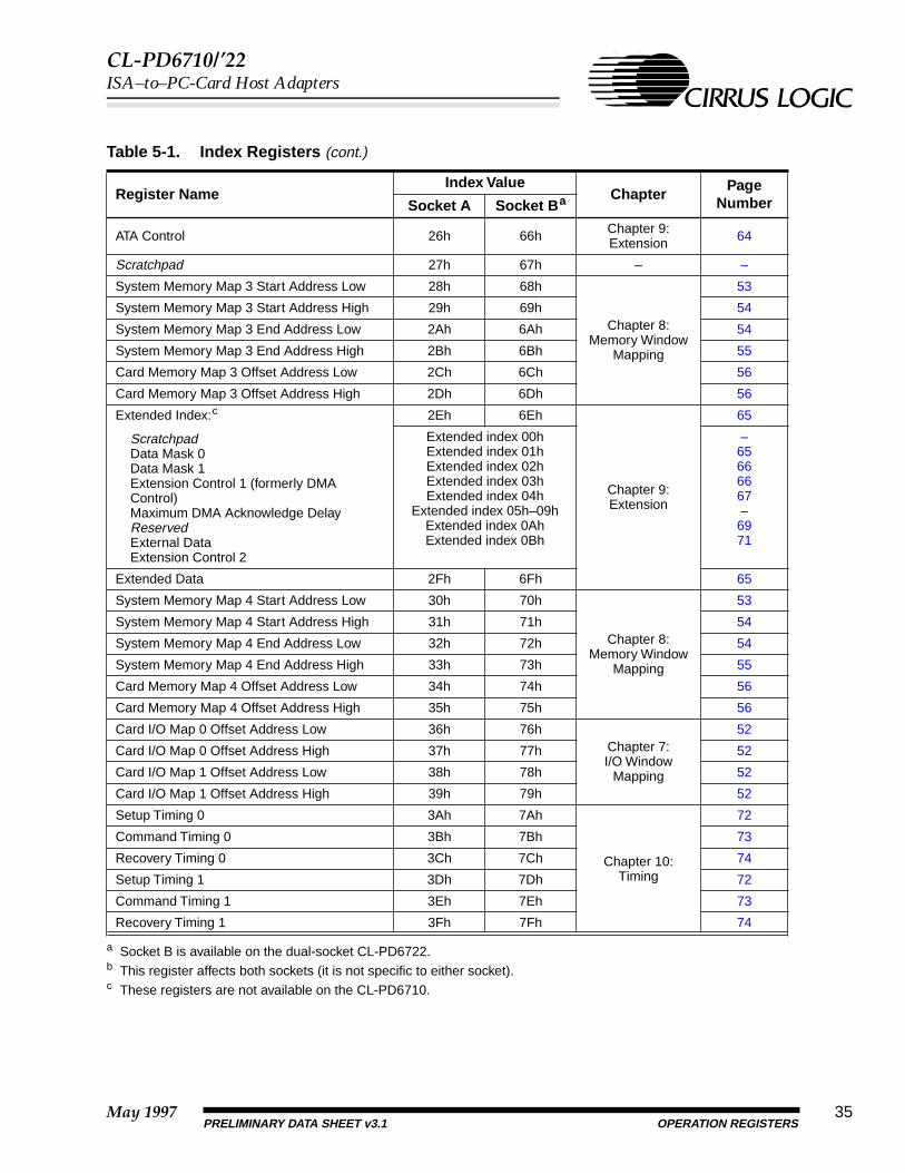
CL-PD6710/’22ISA–to–PC-Card Host Adapters
a Socket B is available on the dual-socket CL-PD6722.b This register affects both sockets (it is not specific to either socket). c These registers are not available on the CL-PD6710.
ATA Control 26h 66h Chapter 9:Extension 64
Scratchpad 27h 67h – –
System Memory Map 3 Start Address Low 28h 68h
Chapter 8:Memory Window
Mapping
53
System Memory Map 3 Start Address High 29h 69h 54
System Memory Map 3 End Address Low 2Ah 6Ah 54
System Memory Map 3 End Address High 2Bh 6Bh 55
Card Memory Map 3 Offset Address Low 2Ch 6Ch 56
Card Memory Map 3 Offset Address High 2Dh 6Dh 56
Extended Index:c
ScratchpadData Mask 0Data Mask 1Extension Control 1 (formerly DMA Control)Maximum DMA Acknowledge DelayReservedExternal DataExtension Control 2
2Eh 6Eh
Chapter 9:Extension
65
Extended index 00hExtended index 01hExtended index 02hExtended index 03hExtended index 04h
Extended index 05h–09hExtended index 0AhExtended index 0Bh
–65666667–
6971
Extended Data 2Fh 6Fh 65
System Memory Map 4 Start Address Low 30h 70h
Chapter 8:Memory Window
Mapping
53
System Memory Map 4 Start Address High 31h 71h 54
System Memory Map 4 End Address Low 32h 72h 54
System Memory Map 4 End Address High 33h 73h 55
Card Memory Map 4 Offset Address Low 34h 74h 56
Card Memory Map 4 Offset Address High 35h 75h 56
Card I/O Map 0 Offset Address Low 36h 76hChapter 7:I/O Window
Mapping
52
Card I/O Map 0 Offset Address High 37h 77h 52
Card I/O Map 1 Offset Address Low 38h 78h 52
Card I/O Map 1 Offset Address High 39h 79h 52
Setup Timing 0 3Ah 7Ah
Chapter 10:Timing
72
Command Timing 0 3Bh 7Bh 73
Recovery Timing 0 3Ch 7Ch 74
Setup Timing 1 3Dh 7Dh 72
Command Timing 1 3Eh 7Eh 73
Recovery Timing 1 3Fh 7Fh 74
Table 5-1. Index Registers (cont.)
Register NameIndex Value
ChapterPage
NumberSocket A Socket Ba
May 1997 35PRELIMINARY DATA SHEET v3.1 OPERATION REGISTERS

CL-PD6710/’22ISA–to–PC-Card Host Adapters
5.2 Data
The Data register is accessed at 03E1h. This register indicates the contents of the register at theDevice/Socket/Register Index selected by the Index register.
Register Name: DataIndex: n/a
Register Per: chipRegister Compatibility Type: 365
Bit 7 Bit 6 Bit 5 Bit 4 Bit 3 Bit 2 Bit 1 Bit 0
Data
PRELIMINARY DATA SHEET v3.1May 199736
OPERATION REGISTERS

CL-PD6710/’22ISA–to–PC-Card Host Adapters
6. CHIP CONTROL REGISTERS
6.1 Chip Revision
Bits 3:0 — Revision
This field indicates compatibility with the 82365SL A-step.
Bits 7:6 — Interface ID
These bits identify what type of interface this controller supports.
a Value for the current stepping only.
Register Name: Chip RevisionIndex: 00h
Register Per: chipRegister Compatibility Type: 365
Bit 7 Bit 6 Bit 5 Bit 4 Bit 3 Bit 2 Bit 1 Bit 0
Interface ID 0 0 Revision
R:10 R:0 R:0 R:0010a
00 I/O only.
01 Memory only.
10 Memory and I/O.
11 Reserved.
May 1997 37PRELIMINARY DATA SHEET v3.1 CHIP CONTROL REGISTERS

CL-PD6710/’22ISA–to–PC-Card Host Adapters
6.2 Interface Status
Bits 1:0 — Battery Voltage Detect
These bits are used by PC Card support software and firmware to indicate the amount of capacityleft in the battery in battery-backed cards in Memory Card Interface mode only. In I/O Card Inter-face mode, bit 0 indicates the state of the BVD1/-STSCHG pin (see page 19). Bit 1 status shouldbe ignored in I/O Card Interface mode.
Bits 3:2 — Card Detect
These bits indicate the state of the -CD1 and -CD2 pins (see page 18).
Bit 4 — Write Protect
This bit indicates the state of the WP/-IOIS16 pin (see page 17) on the card and has meaning onlyin Memory Card Interface mode.
a Bit 7 is the inversion of the value of the -VPP_VALID pin (see page 15).b Bit 5 is the value of the RDY/-IREQ pin (see page 17).c Bit 4 is the value of the WP/-IOIS16 pin (see page 17).d Bits 3:2 are the inversion of the values of the -CD1 and -CD2 pins (see page 18).e Bits 1:0 are the values of the BVD1/-STSCHG and BVD2/-SPKR pins (see page 18).
Register Name: Interface StatusIndex: 01h
Register Per: socketRegister Compatibility Type: 365
Bit 7 Bit 6 Bit 5 Bit 4 Bit 3 Bit 2 Bit 1 Bit 0-VPP_VALID RDY WP -CD2 -CD1 BVD2 BVD1
VPP Valid Card Power On Ready/Busy* Write Protect Card Detect Battery Voltage Detect
Ra R:0 Rb Rc Rd Re
BVD2 Input Level BVD1 Input Level Bit 1 Bit 0 PC Card Interpretation
Low Low 0 0 Card data lost
Low High 0 1 Battery low warning
High Low 1 0 Card data lost
High High 1 1 Battery/data okay
-CD2 Level -CD1 Level Bit 3 Bit 2 Card Detect Status
High High 0 0 Either no card or card is not fully inserted
High Low 0 1 Card is not fully inserted
Low High 1 0 Card is not fully inserted
Low Low 1 1 Card is fully inserted
0 Card is not write protected.
1 Card is write protected.
PRELIMINARY DATA SHEET v3.1May 199738
CHIP CONTROL REGISTERS

CL-PD6710/’22ISA–to–PC-Card Host Adapters
Bit 5 — Ready/Busy*
This bit indicates the state of the RDY/-IREQ pin (see page 17) on the card. If the card has beenconfigured for I/O, then this bit will not be valid.
Bit 6 — Card Power On
This status bit indicates whether power to the card is on. Refer to Table 5-1 on page 34 for details.
Bit 7 — VPP Valid
This bit indicates the status of the -VPP_VALID pin (see page 15).
0 Card is not ready.
1 Card is ready.
0 Power to the card is not on.
1 Power to the card is on.
0 This status bit indicates a logic high at the -VPP_VALID pin.
1 This status bit indicates a logic low at the -VPP_VALID pin.
May 1997 39PRELIMINARY DATA SHEET v3.1 CHIP CONTROL REGISTERS

CL-PD6710/’22ISA–to–PC-Card Host Adapters
6.3 Power Control
Register Name: Power ControlIndex: 02h
Register Per: socketRegister Compatibility Type: 365
Bit 7 Bit 6 Bit 5 Bit 4 Bit 3 Bit 2 Bit 1 Bit 0
Card Enable Compatibility Bit Auto-Power VCC Power Compatibility Bits VPP1 Power
RW:0 RW:0 RW:0 RW:0 RW:00 RW:00
Table 6-1. Enabling of Socket Power Controls
PWR-GOOD Level
Power Control Register -CD1 and
-CD2 Both Active Low
Interface Status Register
(see page 38)-VCC_3
and -VCC_5 Levels
VPP1_PGM and
VPP1_VCC Levels
Bit 4:VCC
Power
Bit 5:Auto- Power
Bit 6: Card Power On
Low X X X 0 Inactive high Inactive low
High 0 X X 0 Inactive high Inactive low
High 1 0 X 1Activated per
Misc Control 1 register, bit 1
Activated per Power Control
register, bits 1 and 0
High 1 1 No 0 Inactive high Inactive low
High 1 1 Yes 1Activated per
Misc Control 1 register, bit 1
Activated per Power Control
register, bits 1 and 0
Table 6-2. Enabling of Outputs to Card Socket
PWR-GOOD Level
-CD1 and -CD2 Both Active Low
Power Control RegisterCL-PD67XX Signal Outputs to SocketBit 4:
VCC PowerBit 7:
Card Enable
Low X X X High impedance
High No X X High impedance
High Yes 0 0 High impedance
High Yes 0 1 Enabled
High Yes 1 0 High impedance
High Yes 1 1 Enabled
PRELIMINARY DATA SHEET v3.1May 199740
CHIP CONTROL REGISTERS

CL-PD6710/’22ISA–to–PC-Card Host Adapters
Bits 1:0 — VPP1 Power
These bits are intended to be used to control the power to the VPP1 pin of the PC Card.
Bit 4 — VCC Power
Depending on the value of bit 5 below, setting this bit to ‘1’ will cause power to be applied to thecard. The VCC 3.3V bit (see page 58) determines whether 3.3V or 5V power is applied.
Bit 5 — Auto-Power
When this bit is set to ‘1’, the CL-PD67XX causes power to the card to be turned on and offautomatically with the insertion and removal of a PC card from the socket.
Bit 7 — Card Enable
When this bit is ‘1’, the outputs to the PC Card are enabled if a card is present and card power isbeing supplied. The pins affected include: -CE2, -CE1, -IORD, -IOWR, -OE, -REG, RESET,A[25:0], D[15:0], and -WE (see page 17).
a Under conditions where VPP1 power is activated. See Table 6.3.
Bit Name Value Description
VCC Power 1 Enables VCC to level described by VCC 3.3V (see page 58)
Auto-Power 1 Enables Auto-power mode
Card Enable 1 Enables socket output drivers
VPP1 PowerBit 1 Bit 0
VPP_PGM VPP_VCC PC Card Intended Socket Function
0 0 Inactive low Inactive low Zero volts to PC Card socket VPP1 pin
0 1 Inactive low Active high a Selected card VCC to PC Card socket VPP1 pin
1 0 Active high a Inactive low +12V to PC Card socket VPP1 pin
1 1 Inactive low Inactive low Zero volts to PC Card socket VPP1 pin
0 Power is not applied to the card: the -VCC_3 and -VCC_5 socket power control pins are inactive high.
1 Power is applied to the card: if bit 5 is ‘0’, or bit 5 is ‘1’ and -CD2 and -CD1 are active low, then the selected -VCC_3 or -VCC_5 socket power control pin is active low.
0 VCC and VPP1 power control signals are activated independent of the socket’s -CD2 and -CD1 input levels.
1 VCC and VPP1 power control signals are only activated if the socket’s -CD2 and -CD1 inputs are active low.
0 Outputs to card socket are not enabled and are floating.
1 Outputs to card socket are enabled if -CD1 and -CD2 are active low and bit 4 is ‘1’.
May 1997 41PRELIMINARY DATA SHEET v3.1 CHIP CONTROL REGISTERS

CL-PD6710/’22ISA–to–PC-Card Host Adapters
6.4 Interrupt and General Control
Bits 3:0 — Card IRQ Select
These bits determine which IRQ will occur when the card causes an interrupt through theRDY/-IREQ pin on the PC Card connector.
Bit 4 — Enable Manage Int
This bit determines how management interrupts will occur.
Bit 5 — Card Is I/O
This bit determines how dual-function socket interface pins will be used.
Register Name: Interrupt and General ControlIndex: 03h
Register Per: socketRegister Compatibility Type: 365
Bit 7 Bit 6 Bit 5 Bit 4 Bit 3 Bit 2 Bit 1 Bit 0
Ring Indicate Enable Card Reset* Card Is I/O Enable
Manage Int Card IRQ Select
RW:0 RW:0 RW:0 RW:0 RW:0000
0000 IRQ disabled
0001 Reserved
0010 Reserved
0011 IRQ 3
0100 IRQ 4
0101 IRQ 5
0110 Reserved
0111 IRQ 7
1000 Reserved
1001 IRQ 9 (On the CL-PD6722, this output may alternately be used as an ISA bus DACK* signal)
1010 IRQ 10 (On the CL-PD6722, this output may alternately be used as an ISA bus DRQ signal)
1011 IRQ 11
1100 IRQ 12 (This output may alternately be used for LED)
1101 Reserved
1110 IRQ 14
1111 IRQ 15 (This output may alternately be used for ring indicate)
0 Card status management interrupts occur as programmed by Management IRQ Select bits (bits 7:4 of Management Interrupt Configuration register, see page 46).
1 Card status management interrupts are redirected to the -INTR line instead of the programmed IRQ pin.
0 Memory Card Interface mode: card socket configured to support memory cards. Dual-function socket interface pins perform memory card-type interface functions.
1 I/O Card Interface mode: card socket configured to support I/O/memory card-type interface functions. Dual-function socket interface pins perform I/O/memory card-type interface functions.
PRELIMINARY DATA SHEET v3.1May 199742
CHIP CONTROL REGISTERS

CL-PD6710/’22ISA–to–PC-Card Host Adapters
Bit 6 — Card Reset*
This bit determines whether the RESET signal (see page 18) to the card is active or inactive.When the Card Enable bit (see page 41) is ‘0’, the RESET signal to the card will be high-imped-ance. See Chapter 10 for further description of ATA mode functions.
Bit 7 — Ring Indicate Enable
This bit determines whether the -STSCHG input pin is used to activate the IRQ15 pin in conjunc-tion with Misc Control 2, IRQ15 Is RI Out (see page 62). This bit has no significance when thecard socket is configured for memory card operation.
0 The RESET signal to the card socket is set active (high for normal, low for ATA mode).
1 The RESET signal to the card socket is set inactive (low for normal, high for ATA mode).
0 BVD1/-STSCHG pin is status change function.
1 BVD1/-STSCHG pin is ring indicate input pin from card.
May 1997 43PRELIMINARY DATA SHEET v3.1 CHIP CONTROL REGISTERS

CL-PD6710/’22ISA–to–PC-Card Host Adapters
6.5 Card Status Change
This register indicates the source of a management interrupt generated by the CL-PD67XX.
NOTE: The corresponding bit in the Management Interrupt Configuration register must be set to ‘1’ to enableeach specific status change detection.
Bit 0 — Battery Dead Or Status Change
When the socket is configured for memory card support, this bit is set to ‘1’ when a BVD1 batterydead high-to-low transition has been detected. When the socket is configured for I/O card support,this bit is set to ‘1’ when the BVD1/-STSCHG pin (see page 19) changes from either high to lowor low to high. This bit is reset to ‘0’ whenever this register is read. In I/O Card Interface mode,function of this bit is not affected by bit 7 of the Interrupt and General Control register.
Bit 1 — Battery Warning Change
When a socket is configured for memory card support, this bit is set to ‘1’ when a high-to-low tran-sition on BVD2 occurs indicating a battery warning was detected. This bit should be ignored whenthe socket is configured for I/O card support. This bit is reset to ‘0’ whenever this register is read.
Bit 2 — Ready Change
When this bit is ‘1’, a change has occurred in the card RDY/-IREQ pin (see page 17). This bit willalways read 0 when the card is configured as an I/O card. This bit is reset to ‘0’ whenever this reg-ister is read.
Bit 3 — Card Detect Change
When this bit is ‘1’, a change has occurred on the -CD1 or -CD2 pins (see page 18). This bit isreset to ‘0’ whenever this register is read.
Register Name: Card Status ChangeIndex: 04h
Register Per: socketRegister Compatibility Type: 365
Bit 7 Bit 6 Bit 5 Bit 4 Bit 3 Bit 2 Bit 1 Bit 0
0 0 0 0 Card Detect Change
Ready Change
Battery Warning Change
Battery Dead Or Status Change
R:0 R:0 R:0 R:0 R:0 R:0 R:0 R:0
0 A transition (from high to low for memory card support or either high to low or low to high for I/O card support) on the BVD1/-STSCHG pin has not occurred since this register was last read.
1 A transition on the BVD1/-STSCHG pin has occurred.
0 A transition (from high to low) on the BVD2 pin has not occurred since this register was last read.
1 A transition on the BVD2 pin has occurred.
0 A transition on the RDY/-IREQ pin has not occurred since this register was last read.
1 A transition on the RDY/-IREQ pin has occurred.
0 A transition on the -CD1 or -CD2 pins has not occurred since this register was last read.
1 A transition on the -CD1 or -CD2 pins has occurred.
PRELIMINARY DATA SHEET v3.1May 199744
CHIP CONTROL REGISTERS

CL-PD6710/’22ISA–to–PC-Card Host Adapters
6.6 Management Interrupt Configuration
This register controls which status changes may cause management interrupts and at which pin the man-agement interrupts will appear.
Bit 0 — Battery Dead Or Status Change Enable
When this bit is ‘1’, a management interrupt will occur when the Card Status Change register’sBattery Dead Or Status Change bit (see page 44) is ‘1’. This allows management interrupts to begenerated on changes in level of the BVD1/-STSCHG pin.
Bit 1 — Battery Warning Enable
When this bit is ‘1’, a management interrupt will occur when the Card Status Change register’sBattery Warning Change bit (see page 44) is ‘1’. This bit is ignored when the card socket is in I/Omode.
Bit 2 — Ready Enable
When this bit is ‘1’, a management interrupt will occur when the Card Status Change register’sReady Change bit (see page 44) is ‘1’.
Bit 3 — Card Detect Enable
When this bit is ‘1’, a management interrupt will occur when the Card Status Change register’sCard Detect Change bit (see page 44) is ‘1’.
Register Name: Management Interrupt ConfigurationIndex: 05h
Register Per: socketRegister Compatibility Type: 365
Bit 7 Bit 6 Bit 5 Bit 4 Bit 3 Bit 2 Bit 1 Bit 0
Management IRQ Select Card Detect Enable Ready Enable
Battery Warning Enable
Battery Dead Or Status Change Enable
RW:0000 RW:0 RW:0 RW:0 RW:0
0 Battery Dead Or Status Change management interrupt disabled.
1 If Battery Dead Or Status Change is ‘1’, a management interrupt will occur.
0 Battery Warning Change management interrupt disabled.
1 If Battery Warning Change is ‘1’, a management interrupt will occur.
0 Ready Change management interrupt disabled.
1 If Ready Change is ‘1’, a management interrupt will occur.
0 Card Detect Change management interrupt disabled.
1 If Card Detect Change is ‘1’, a management interrupt will occur.
May 1997 45PRELIMINARY DATA SHEET v3.1 CHIP CONTROL REGISTERS

CL-PD6710/’22ISA–to–PC-Card Host Adapters
Bits 7:4 — Management IRQ Select
These bits determine which interrupt pin will be used for card status change management inter-rupts.
0000 IRQ disabled
0001 Reserved
0010 Reserved
0011 IRQ 3
0100 IRQ 4
0101 IRQ 5
0110 Reserved
0111 IRQ 7
1000 Reserved
1001 IRQ 9 (On the CL-PD6722, this output may alternately be used as an ISA bus DACK* signal)
1010 IRQ 10 (On the CL-PD6722, this output may alternately be used as an ISA bus DRQ signal)
1011 IRQ 11
1100 IRQ 12 (This output may alternately be used for LED)
1101 Reserved
1110 IRQ 14
1111 IRQ 15 (This output may alternately be used for ring indicate)
PRELIMINARY DATA SHEET v3.1May 199746
CHIP CONTROL REGISTERS

CL-PD6710/’22ISA–to–PC-Card Host Adapters
6.7 Mapping Enable
Bit 0 — Memory Map 0 Enable
When this bit is ‘1’, the Memory Mapping registers for Memory Space 0 will be enabled and thecontroller will respond to memory accesses in the memory space defined by those registers.
Bit 1 — Memory Map 1 Enable
When this bit is ‘1’, the Memory Mapping registers for Memory Space 1 will be enabled and thecontroller will respond to memory accesses in the memory space defined by those registers.
Bit 2 — Memory Map 2 Enable
When this bit is ‘1’, the Memory Mapping registers for Memory Space 2 will be enabled and thecontroller will respond to memory accesses in the memory space defined by those registers.
Bit 3 — Memory Map 3 Enable
When this bit is ‘1’, the Memory Mapping registers for Memory Space 3 will be enabled and thecontroller will respond to memory accesses in the memory space defined by those registers.
Bit 4 — Memory Map 4 Enable
When this bit is ‘1’, the Memory Mapping registers for Memory Space 4 will be enabled and thecontroller will respond to memory accesses in the memory space defined by those registers.
Bit 5 — MEMCS16 Full Decode
This bit is not used. All addresses are used to determine the level of MEMCS16*.
Register Name: Mapping EnableIndex: 06h
Register Per: socketRegister Compatibility Type: 365
Bit 7 Bit 6 Bit 5 Bit 4 Bit 3 Bit 2 Bit 1 Bit 0
I/O Map 1 Enable
I/O Map 0 Enable
MEMCS16 Full Decode
Memory Map 4 Enable
Memory Map 3 Enable
Memory Map 2 Enable
Memory Map 1 Enable
Memory Map 0 Enable
RW:0 RW:0 RW:0 RW:0 RW:0 RW:0 RW:0 RW:0
0 Memory Mapping registers for Memory Space 0 disabled.
1 Memory Mapping registers for Memory Space 0 enabled.
0 Memory Mapping registers for Memory Space 1 disabled.
1 Memory Mapping registers for Memory Space 1 enabled.
0 Memory Mapping registers for Memory Space 2 disabled.
1 Memory Mapping registers for Memory Space 2 enabled.
0 Memory Mapping registers for Memory Space 3 disabled.
1 Memory Mapping registers for Memory Space 3 enabled.
0 Memory Mapping registers for Memory Space 4 disabled.
1 Memory Mapping registers for Memory Space 4 enabled.
May 1997 47PRELIMINARY DATA SHEET v3.1 CHIP CONTROL REGISTERS

CL-PD6710/’22ISA–to–PC-Card Host Adapters
Bit 6 — I/O Map 0 Enable
When this bit is ‘1’, the I/O Mapping registers for I/O Space 0 will be enabled and the controller willrespond to I/O accesses in the I/O space defined by those registers.
Bit 7 — I/O Map 1 Enable
When this bit is ‘1’, the I/O Mapping registers for I/O Space 1 will be enabled and the controller willrespond to I/O accesses in the I/O space defined by those registers.
0 I/O Mapping registers for I/O Space 0 disabled.
1 I/O Mapping registers for I/O Space 0 enabled.
0 I/O Mapping registers for I/O Space 1 disabled.
1 I/O Mapping registers for I/O Space 1 enabled.
PRELIMINARY DATA SHEET v3.1May 199748
CHIP CONTROL REGISTERS

CL-PD6710/’22ISA–to–PC-Card Host Adapters
7. I/O WINDOW MAPPING REGISTERS
The I/O windows must never include 3E0h and 3E1h.
7.1 I/O Window Control
Bit 0 — I/O Window 0 Size
When bit 1 below is ‘0’, this bit determines the size of the data path to I/O Window 0. When bit 1is ‘1’, this bit is ignored.
Bit 1 — Auto-Size I/O Window 0
This bit determines the data path to I/O Window 0. Note that when this bit is ‘1’, the -IOIS16 signal(see page 17) determines the width of the data path to the card.
Bit 3 — Timing Register Select 0
This bit determines the access timing specification for I/O Window 0 (see page 72).
Bit 4 — I/O Window 1 Size
When bit 5 below is ‘0’, this bit determines the size of the data path to I/O Window 1. When bit 5is ‘1’, this bit is ignored.
Bit 5 — Auto-Size I/O Window 1
This bit determines the width of the data path to I/O Window 1. Note that when this bit is ‘1’, the-IOIS16 signal (see page 17) determines the window size. This bit must be set for proper ATAmode operation (see Chapter 11).
Register Name: I/O Window ControlIndex: 07h
Register Per: socketRegister Compatibility Type: 365
Bit 7 Bit 6 Bit 5 Bit 4 Bit 3 Bit 2 Bit 1 Bit 0
Timing Register Select 1
Compatibility Bit
Auto-Size I/O Window 1
I/O Window 1 Size
Timing Register Select 0
Compatibility Bit
Auto-Size I/O Window 0
I/O Window 0 Size
RW:0 RW:0 RW:0 RW:0 RW:0 RW:0 RW:0 RW:0
0 8-bit data path to I/O Window 0.
1 16-bit data path to I/O Window 0.
0 I/O Window 0 Size (see bit 0 above) determines the data path to I/O Window 0.
1 The data path to I/O Window 0 will be determined based on -IOIS16 returned by the card.
0 Accesses made with timing specified in Timing Set 0.
1 Accesses made with timing specified in Timing Set 1.
0 8-bit data path to I/O Window 1.
1 16-bit data path to I/O Window 1.
0 I/O Window 1 Size (see bit 4) determines the data path to I/O Window 1.
1 The data path to I/O Window 1 will be determined based on -IOIS16 returned by the card.
May 1997 49PRELIMINARY DATA SHEET v3.1 I/O WINDOW MAPPING REGISTERS

CL-PD6710/’22ISA–to–PC-Card Host Adapters
May 199750
Bit 7 — Timing Register Select 1
This bit determines the access timing specification for I/O Window 1 (see page 72).
7.2 System I/O Map 0–1 Start Address Low
There are two separate System I/O Map Start Address Low registers, each with identical fields. Theseregisters are located at the following indexes:
Index System I/O Map Start Address Low
8h System I/O Map 0 Start Address LowCh System I/O Map 1 Start Address Low
Bits 7:0 — Start Address 7:0
This register contains the least-significant byte of the address that specifies the beginning of theI/O space within the corresponding I/O map. I/O accesses that are equal or above this addressand equal or below the corresponding System I/O Map End Address will be mapped into the I/Ospace of the corresponding PC Card.
The most-significant byte is located in the System I/O Map 0–1 Start Address High register (seepage 50).
7.3 System I/O Map 0–1 Start Address High
There are two separate System I/O Map Start Address High registers, each with identical fields. Theseregisters are located at the following indexes:
Index System I/O Map Start Address High
9h System I/O Map 0 Start Address HighDh System I/O Map 1 Start Address High
Bits 15:8 — Start Address 15:8
This register contains the most-significant byte of the Start Address. See the description of the StartAddress field associated with bits 7:0 of the System I/O Map 0–1 Start Address Low register.
0 Accesses made with timing specified in Timing Set 0.
1 Accesses made with timing specified in Timing Set 1.
Register Name: System I/O Map 0–1 Start Address LowIndex: 08h, 0Ch
Register Per: socketRegister Compatibility Type: 365
Bit 7 Bit 6 Bit 5 Bit 4 Bit 3 Bit 2 Bit 1 Bit 0
Start Address 7:0
RW:00000000
Register Name: System I/O Map 0–1 Start Address HighIndex: 09h, 0Dh
Register Per: socketRegister Compatibility Type: 365
Bit 7 Bit 6 Bit 5 Bit 4 Bit 3 Bit 2 Bit 1 Bit 0
Start Address 15:8
RW:00000000
PRELIMINARY DATA SHEET v3.1I/O WINDOW MAPPING REGISTERS

CL-PD6710/’22ISA–to–PC-Card Host Adapters
7.4 System I/O Map 0–1 End Address Low
There are two separate System I/O Map End Address Low registers, each with identical fields. These reg-isters are located at the following indexes:
Index System I/O Map End Address Low
Ah System I/O Map 0 End Address LowEh System I/O Map 1 End Address Low
Bits 7:0 — End Address 7:0
This register contains the least-significant byte of the address that specifies the termination of theI/O space within the corresponding I/O map. I/O accesses that are equal or below this addressand equal or above the corresponding System I/O Map Start Address will be mapped into the I/Ospace of the corresponding PC Card.
The most-significant byte is located in the System I/O Map 0–1 End Address High register (seepage 51).
7.5 System I/O Map 0–1 End Address High
There are two separate System I/O Map End Address High registers, each with identical fields. Theseregisters are located at the following indexes:
Index System I/O Map End Address High
Bh System I/O Map 0 End Address HighFh System I/O Map 1 End Address High
Bits 15:8 — End Address 15:8
This register contains the most-significant byte of the End Address. See the description of the EndAddress field associated with bits 7:0 of the System I/O Map 0–1 End Address Low register (seepage 51).
Register Name: System I/O Map 0–1 End Address LowIndex: 0Ah, 0Eh
Register Per: socketRegister Compatibility Type: 365
Bit 7 Bit 6 Bit 5 Bit 4 Bit 3 Bit 2 Bit 1 Bit 0
End Address 7:0
RW:00000000
Register Name: System I/O Map 0–1 End Address HighIndex: 0Bh, 0Fh
Register Per: socketRegister Compatibility Type: 365
Bit 7 Bit 6 Bit 5 Bit 4 Bit 3 Bit 2 Bit 1 Bit 0
End Address 15:8
RW:00000000
May 1997 51PRELIMINARY DATA SHEET v3.1 I/O WINDOW MAPPING REGISTERS

CL-PD6710/’22ISA–to–PC-Card Host Adapters
7.6 Card I/O Map 0–1 Offset Address Low
There are two separate Card I/O Map Offset Address Low registers, each with identical fields. These reg-isters are located at the following indexes:
Index Card I/O Map Offset Address Low
36h Card I/O Map 0 Offset Address Low38h Card I/O Map 1 Offset Address Low
Bits 7:1 — Offset Address 7:1
This register contains the least-significant byte of the quantity that will be added to the host I/Oaddress; this will determine the PC Card I/O map location where the I/O access will occur.
The most-significant byte is located in the Card I/O Map 0–1 Offset Address High register (seepage 52).
7.7 Card I/O Map 0–1 Offset Address High
There are two separate Card I/O Map Offset Address High registers, each with identical fields. These reg-isters are located at the following indexes:
Index Card I/O Map Offset Address High
37h Card I/O Map 0 Offset Address High39h Card I/O Map 1 Offset Address High
Bits 15:8 — Offset Address 15:8
This register contains the most-significant byte of the Offset Address. See the description of theEnd Address field associated with bits 7:1 of the Card I/O Map 0–1 Offset Address Low register(see page 52).
a This bit must be programmed to ‘0’.
Register Name: Card I/O Map 0–1 Offset Address LowIndex: 36h, 38h
Register Per: socketRegister Compatibility Type: ext.
Bit 7 Bit 6 Bit 5 Bit 4 Bit 3 Bit 2 Bit 1 Bit 0
Offset Address 7:1 0 a
RW:0000000 RW:0
Register Name: Card I/O Map 0–1 Offset Address HighIndex: 37h, 39h
Register Per: socketRegister Compatibility Type: ext.
Bit 7 Bit 6 Bit 5 Bit 4 Bit 3 Bit 2 Bit 1 Bit 0
Offset Address 15:8
RW:00000000
PRELIMINARY DATA SHEET v3.1May 199752
I/O WINDOW MAPPING REGISTERS

CL-PD6710/’22ISA–to–PC-Card Host Adapters
8. MEMORY WINDOW MAPPING REGISTERS
The following information about the memory map windows is important:
● The memory window mapping registers determine where in the ISA memory space and PC Card memoryspace accesses will occur. There are five memory windows that can be used independently.
● The memory windows are enabled and disabled using the Mapping Enable register (see page 47).
● To specify where in the ISA space a memory window is mapped, start and end addresses are specified. Amemory window is selected whenever the appropriate Memory Map Enable bit (see page 47) is set, andwhen the ISA address is greater than or equal to the appropriate System Memory Map Start Address reg-ister (see page 53) and the ISA address is less than or equal to the appropriate System Memory Map EndAddress register (see page 54).
● Start and end addresses are specified with ISA Address bits 23:12. This sets the minimum size of a memorywindow to 4K bytes. Memory windows are specified in the ISA address from 64 Kbytes to 16 Mbytes(0010000h–FFFFFFh). Note that no memory window can be mapped in the first 64 Kbytes of the ISA addressspace.
● To ensure proper operation, none of the windows can overlap in the ISA address space.
8.1 System Memory Map 0–4 Start Address Low
There are five separate System Memory Map Start Address Low registers, each with identical fields.These registers are located at the following indexes:
Index System Memory Map Start Address Low
10h System Memory Map 0 Start Address Low18h System Memory Map 1 Start Address Low20h System Memory Map 2 Start Address Low28h System Memory Map 3 Start Address Low30h System Memory Map 4 Start Address Low
Bits 7:0 — Start Address 19:12
This register contains the least-significant byte of the address that specifies where in the memoryspace the corresponding memory map will begin. Memory accesses that are equal or above thisaddress and equal or below the corresponding System Memory Map End Address will be mappedinto the memory space of the corresponding PC Card.
The most-significant four bits are located in the System Memory Map 0–4 Start Address Highregister (see page 54).
Register Name: System Memory Map 0–4 Start Address LowIndex: 10h, 18h, 20h, 28h, 30h
Register Per: socketRegister Compatibility Type: 365
Bit 7 Bit 6 Bit 5 Bit 4 Bit 3 Bit 2 Bit 1 Bit 0
Start Address 19:12
RW:00000000
May 1997 53PRELIMINARY DATA SHEET v3.1 MEMORY WINDOW MAPPING REGISTERS

CL-PD6710/’22ISA–to–PC-Card Host Adapters
8.2 System Memory Map 0–4 Start Address High
There are five separate System Memory Map Start Address High registers, each with identical fields.These registers are located at the following indexes:
Index System Memory Map Start Address High
11h System Memory Map 0 Start Address High19h System Memory Map 1 Start Address High21h System Memory Map 2 Start Address High29h System Memory Map 3 Start Address High31h System Memory Map 4 Start Address High
Bits 3:0 — Start Address 23:20
This field contains the most-significant four bits of the Start Address. See the description of theStart Address field associated with bits 7:0 of the System Memory Map 0–4 Start Address Lowregister (see page 53).
Bit 7 — Window Data Size
This bit determines the data path size to the card.
8.3 System Memory Map 0–4 End Address Low
There are five separate System Memory Map End Address Low registers, each with identical fields.These registers are located at the following indexes:
Index System Memory Map End Address Low
12h System Memory Map 0 End Address Low1Ah System Memory Map 1 End Address Low22h System Memory Map 2 End Address Low2Ah System Memory Map 3 End Address Low32h System Memory Map 4 End Address Low
Register Name: System Memory Map 0–4 Start Address HighIndex: 11h, 19h, 21h, 29h, 31h
Register Per: socketRegister Compatibility Type: 365
Bit 7 Bit 6 Bit 5 Bit 4 Bit 3 Bit 2 Bit 1 Bit 0
Window Data Size
Compatibility Bit Scratchpad Bits Start Address 23:20
RW:0 RW:0 RW:00 RW:0000
0 8-bit data path to the card.
1 16-bit data path to the card.
Register Name: System Memory Map 0–4 End Address LowIndex: 12h, 1Ah, 22h, 2Ah, 32h
Register Per: socketRegister Compatibility Type: 365
Bit 7 Bit 6 Bit 5 Bit 4 Bit 3 Bit 2 Bit 1 Bit 0
End Address 19:12
RW:00000000
PRELIMINARY DATA SHEET v3.1May 199754
MEMORY WINDOW MAPPING REGISTERS

CL-PD6710/’22ISA–to–PC-Card Host Adapters
Bits 7:0 — End Address 19:12
This register contains the least-significant byte of the address that specifies where in the memoryspace the corresponding memory map will end. Memory accesses that are equal or below thisaddress and equal or above the corresponding System Memory Map Start Address will bemapped into the memory space of the corresponding PC Card.
The most-significant four bits are located in the System Memory Map 0–4 End Address Highregister (see Section 8.4).
8.4 System Memory Map 0–4 End Address High
There are five separate System Memory Map End Address High registers, each with identical fields.These registers are located at the following indexes:
Index System Memory Map End Address High
13h System Memory Map 0 End Address High1Bh System Memory Map 1 End Address High23h System Memory Map 2 End Address High2Bh System Memory Map 3 End Address High33h System Memory Map 4 End Address High
Bits 3:0 — End Address 23:20
This field contains the most-significant four bits of the End Address. See the description of the EndAddress field associated with bits 7:0 of the System Memory Map 0–4 End Address Low regis-ter (see page 54).
Bits 7:6 — Card Timer Select
This field selects the Timeset registers used to control socket timing for card accesses in thiswindow address range. Timeset 0 and 1 reset to values compatible with PC Card standards. Themapping of bits 7:6 to Timeset 0 and 1, as shown in the preceding table, is done for softwarecompatibility with older ISA bus-based PCMCIA host adapters that use ISA bus wait states insteadof Timeset registers (see page 72).
Register Name: System Memory Map 0–4 End Address HighIndex: 13h, 1Bh, 23h, 2Bh, 33h
Register Per: socketRegister Compatibility Type: 365
Bit 7 Bit 6 Bit 5 Bit 4 Bit 3 Bit 2 Bit 1 Bit 0
Card Timer Select Scratchpad Bits End Address 23:20
RW:00 RW:00 RW:0000
00 Selects Timer Set 0.
01 Selects Timer Set 1.
10 Selects Timer Set 1.
11 Selects Timer Set 1.
May 1997 55PRELIMINARY DATA SHEET v3.1 MEMORY WINDOW MAPPING REGISTERS

CL-PD6710/’22ISA–to–PC-Card Host Adapters
8.5 Card Memory Map 0–4 Offset Address Low
There are five separate Card Memory Map Offset Address Low registers, each with identical fields. Theseregisters are located at the following indexes:
Index Card Memory Map Offset Address Low
14h Card Memory Map 0 Offset Address Low1Ch Card Memory Map 1 Offset Address Low24h Card Memory Map 2 Offset Address Low2Ch Card Memory Map 3 Offset Address Low34h Card Memory Map 4 Offset Address Low
Bits 7:0 — Offset Address 19:12
This register contains the least-significant byte of the quantity that will be added to the hostmemory address, which will determine where the memory access will occur in the PC Cardmemory map.
The most-significant six bits are located in the Card Memory Map 0–4 Offset Address Highregister (see page 56).
8.6 Card Memory Map 0–4 Offset Address High
There are five separate Card Memory Map Offset Address High registers, each with identical fields. Theseregisters are located at the following indexes:
Index Card Memory Map Offset Address High
15h Card Memory Map 0 Offset Address High1Dh Card Memory Map 1 Offset Address High25h Card Memory Map 2 Offset Address High2Dh Card Memory Map 3 Offset Address High35h Card Memory Map 4 Offset Address High
Register Name: Card Memory Map 0–4 Offset Address LowIndex: 14h, 1Ch, 24h, 2Ch, 34h
Register Per: socketRegister Compatibility Type: 365
Bit 7 Bit 6 Bit 5 Bit 4 Bit 3 Bit 2 Bit 1 Bit 0
Offset Address 19:12
RW:00000000
Register Name: Card Memory Map 0–4 Offset Address HighIndex: 15h, 1Dh, 25h, 2Dh, 35h
Register Per: socketRegister Compatibility Type: 365
Bit 7 Bit 6 Bit 5 Bit 4 Bit 3 Bit 2 Bit 1 Bit 0
Write Protect REG Setting Offset Address 25:20
RW:0 RW:0 RW:000000
PRELIMINARY DATA SHEET v3.1May 199756
MEMORY WINDOW MAPPING REGISTERS

CL-PD6710/’22ISA–to–PC-Card Host Adapters
Bits 5:0 — Offset Address 25:20
This field contains the most-significant six bits of the Offset Address. See the description of theOffset Address field associated with bits 7:0 of the Card Memory Map 0–4 Offset Address Lowregister (see page 56).
Bit 6 — REG Setting
This bit determines whether -REG (see page 16) will be active for accesses made through thiswindow. Card Information Structure (CIS) memory is accessed by setting this bit to ‘1’.
Bit 7 — Write Protect
This bit determines whether writes to the card through this window are allowed. This bit only ap-plies to Memory Card Interface mode.
NOTE: This bit must be set to ‘0’ and a memory card’s ‘WP’ switch must be turned off to allow writes to a card usinga memory interface, such as an SRAM card.
0 -REG (see page 16) is not active for accesses made through this window.
1 -REG is active for accesses made through this window.
0 Writes to the card through this window are allowed.
1 Writes to the card through this window are inhibited.
May 1997 57PRELIMINARY DATA SHEET v3.1 MEMORY WINDOW MAPPING REGISTERS

CL-PD6710/’22ISA–to–PC-Card Host Adapters
9. EXTENSION REGISTERS
9.1 Misc Control 1
Bit 0 — 5 V Detect (CL-PD6710 only)
This bit is connected to pins VS1 and VS2. Cards that will only operate at 3.3 V will drive this bitto ‘0’.
Bit 1 — VCC 3.3V
This bit determines which output pin is to be used to enable VCC power to the socket when cardpower is to be applied; it is used in conjunction with bits 5:4 of the Power Control register (seepage 40).
Bit 2 — Pulse Management Interrupt
This bit selects Level or Pulse mode operation of the IRQ[XX] or -INTR pin being used for cardstatus change management interrupts (see page 14). Note that a clock must be present on theincoming CLK for pulsed interrupts to work.
a On some versions of the CL-PD6722, this bit can be used to read levels of the A_GPSTB and B_GPSTB pins. Contact Cirrus Logic for more information.
Register Name: Misc Control 1Index: 16h
Register Per: socketRegister Compatibility Type: ext.
Bit 7 Bit 6 Bit 5 Bit 4 Bit 3 Bit 2 Bit 1 Bit 0
Inpack Enable Scratchpad Bits Speaker Enable
Pulse System IRQ
Pulse Management
InterruptVCC 3.3V
5 V Detect (CL-PD6710)
Reserved a (CL-PD6722)
RW:0 RW:00 RW:0 RW:0 RW:0 RW:0 R:X W:0
0 3.3 V card detected.
1 Old or 5 V card detected.
0 -VCC_5 activated when card power is to be applied.
1 -VCC_3 activated when card power is to be applied.
0 Card status change management interrupts are passed to the appropriate IRQ[XX] or -INTR pin as level-sensitive.
1 When a card status change management interrupt occurs, the appropriate IRQ[XX] or -INTR pin is driven with the pulse train shown in Figure 9-1 and allows for interrupt sharing.
PRELIMINARY DATA SHEET v3.1May 199758
EXTENSION REGISTERS

CL-PD6710/’22ISA–to–PC-Card Host Adapters
Figure 9-1. Pulse Mode Interrupts
Bit 3 — Pulse System IRQ
This bit selects Level or Pulse mode operation of the IRQ[XX] pins for interrupts from a PC CardRDY/-IREQ pin (see page 17).
Bit 4 — Speaker Enable
This bit determines whether the card -SPKR pin will drive SPKR_OUT* (see page 15).
Bit 7 — Inpack Enable
This bit is used to determine when to drive data onto the ISA bus.
0 RDY/-IREQ generated interrupts are passed to the IRQ[XX] pin as level-sensitive.
1 When a RDY/-IREQ interrupt occurs, the IRQ[XX] pin is driven with the pulse train shown in Figure 9-1 and allows for interrupt sharing.
0 SPKR_OUT* is high-impedance.
1 SPKR_OUT* is driven from the XOR of -SPKR from each enabled socket.
0 -INPACK pin (see page 17) ignored.
1 -INPACK pin used to control data bus drivers during I/O read from the socket.
-INTR orHigh-Z High-Z
IRQ[XX] Driven low
Driven high
May 1997 59PRELIMINARY DATA SHEET v3.1 EXTENSION REGISTERS

CL-PD6710/’22ISA–to–PC-Card Host Adapters
9.2 FIFO Control
Bit 7 — Empty Write FIFO
This bit controls FIFO operation and reports FIFO status. When this bit is written to ‘1’, all data inthe FIFO is lost. During read operations when this bit is ‘1’, the FIFO is empty. During read oper-ations when this bit is ‘0’, data is still in the FIFO. This bit is used to ensure the FIFO is empty be-fore changing timing registers.
FIFO contents will be lost whenever any of the following occur:
● PWRGOOD pin (see page 13) is ‘0’.
● The card is removed.
● VCC Power bit (see page 41) is programmed to ‘0’.
a Because a write will flush the FIFO, these scratchpad bits should be used only when card activity is guaranteed not to occur.
Register Name: FIFO ControlIndex: 17h
Register Per: socketRegister Compatibility Type: ext.
Bit 7 Bit 6 Bit 5 Bit 4 Bit 3 Bit 2 Bit 1 Bit 0
Empty Write FIFO Scratchpad Bitsa
RW RW:0000000
Value I/O Read I/O Write
0 FIFO not empty No operation occurs; default on reset
1 FIFO empty Flush the FIFO
PRELIMINARY DATA SHEET v3.1May 199760
EXTENSION REGISTERS
CL-PD6710/’22ISA–to–PC-Card Host Adapters
9.3 Misc Control 2
Bit 0 — Bypass Frequency Synthesizer
This bit determines internal time base.
Bit 1 — Low-Power Dynamic Mode
This bit determines whether Low-Power Dynamic mode is enabled. For maximum operationalpower savings, keep this bit set to ‘1’.
Bit 2 — Suspend
This bit enables Suspend mode. After entering Suspend, AEN should be pulled high for lowestpower consumption. When this bit is high and AEN is high, all ISA bus interface inputs are turnedoff. In 82386SL systems when the processor is in Suspend mode, the ISA bus interface signalsfloat; this feature will prevent high current flow in the CL-PD67XX inputs.
Bit 3 — 5V Core
This bit selects input threshold circuits for use when 3.3 or 5.0 volts is connected to theCL-PD67XX CORE_VDD pins. This bit must be set to ‘0’ when the CORE_VDD pins are connect-ed to 3.3 volts to preserve TTL-compatible input thresholds to the card socket.
Bit 4 — Drive LED Enable
NOTE:This bit should be set to ‘0’ if in Memory Card Interface mode.
This bit determines whether -SPKR is used to drive an LED on the IRQ12 (see page 14) for diskdrives.
Register Name: Misc Control 2Index: 1Eh
Register Per: chipRegister Compatibility Type: ext.
Bit 7 Bit 6 Bit 5 Bit 4 Bit 3 Bit 2 Bit 1 Bit 0
IRQ15 Is RI Out
DMA System (CL-PD6722)
Three-State Bit 7
Drive LED Enable 5V Core Suspend
Low-Power Dynamic
Mode
Bypass Frequency Synthesizer
RW:0 RW:0 RW:0 RW:0 RW:0 RW:0 RW:1 RW:0
0 Normal operation, internal clock = CLK input frequency x 7/4.
1 Internal clock = CLK input frequency (see page 15).
0 Clock runs always.
1 Normal operation, stop clock when possible.
0 Normal operation.
1 Stop Frequency Synthesizer, enable all Low-Power modes and disable socket access.
0 Normal operation: use when CORE_VDD pin is connected to 3.3 volts.
1 Selects input thresholds for use when 5.0 volts is connected to the CL-PD67XX CORE_VDD pins.
0 IRQ12 operates normally.
1 IRQ12 becomes an open-drain output suitable for driving an LED (driven whenever the card -SPKR output is turned on, and the corresponding Speaker Is LED input bit (see page 64) is set).
May 1997 61PRELIMINARY DATA SHEET v3.1 EXTENSION REGISTERS

CL-PD6710/’22ISA–to–PC-Card Host Adapters
Bit 5 — Three-State Bit 7
This bit enables floppy change bit compatibility.
Bit 6 — DMA System (CL-PD6722 only)
On the CL-PD6710, this bit is reserved.
On the CL-PD6722, this bit is used to configure system interface signals for normal or DMA oper-ation. At reset, the signals IRQ9, IRQ10, and -VPP_VALID are in non-DMA mode, and this bit isset to ‘0’. When this bit is set to ‘1’, the IRQ9, IRQ10, and -VPP_VALID pins are reconfigured forsystem bus DMA interfacing. Refer to Chapter 14 for a functional description of these pins duringDMA operation.
Bit 7 — IRQ15 Is RI Out
This bit determines the function of the IRQ15 pin. When configured for ring indicate, IRQ15 is usedto resume a processor with NMI or SMI such as an 82486SL when a high-to-low change is detect-ed on the -STSCHG pin.
0 Normal operation.
1 For socket I/O at address 03F7h and 0377h, do not drive bit 7.
0 Configured for non-DMA mode on the CL-PD6722.
1 Configured for DMA mode on the CL-PD6722.
0 Normal IRQ15 operation.
1 IRQ15 is connected to Ring Indicate pin on the host processor.
PRELIMINARY DATA SHEET v3.1May 199762
EXTENSION REGISTERS

CL-PD6710/’22ISA–to–PC-Card Host Adapters
9.4 Chip Information
Bits 4:1 — CL-PD67XX Revision Level
This field identifies the revision of the controller. The initial value is ‘111’. Contact Cirrus Logic formore information on revision levels for the CL-PD6710 and CL-PD6722.
Bit 5 — Dual/Single Socket*
This bit specifies the number of sockets supported by the CL-PD67XX.
Bits 7:6 — Cirrus Logic Host-Adapter Identification
This field identifies a Cirrus Logic host-adapter device. After chip reset or doing an I/O write to thisregister, the first read of this register will return ‘11’. On the next read, this field will be ‘00’. Thispattern of toggling data on subsequent reads can be used by software to determine presence ofa Cirrus Logic host adapter in a system or to determine occurrence of a device reset.
a The value for CL-PD6710 is ‘0’, and the value for CL-PD6722 is ‘1’.b This read-only value depends on the revision level of the CL-PD67XX chip.c The value for CL-PD6722 is ‘1’. The value for the CL-PD6710 is ‘0’.
Register Name: Chip InformationIndex: 1Fh
Register Per: chipRegister Compatibility Type: ext.
Bit 7 Bit 6 Bit 5 Bit 4 Bit 3 Bit 2 Bit 1 Bit 0
Cirrus Logic Host-Adapter Identification
Dual/Single Socket* CL-PD67XX Revision Level Reserved
R:11 R:na R:nnnnb R:nc
0 Chip identified as a single-socket controller.
1 Chip identified as a dual-socket controller.
00 Second read after I/O write to this register.
11 First read after I/O write to this register.
May 1997 63PRELIMINARY DATA SHEET v3.1 EXTENSION REGISTERS

CL-PD6710/’22ISA–to–PC-Card Host Adapters
9.5 ATA Control
Bit 0 — ATA Mode
This bit reconfigures the particular socket as an ATA drive interface. Refer to Table 11-1 onpage 75 for PC Card socket pin definitions in ATA mode.
Bit 1 — Speaker Is LED Input
This bit changes the function of the BVD2/-SPKR/-LED pin (see page 18) from digital speaker in-put to disk status LED input. When in I/O Card Interface mode or ATA mode, setting this bit to ‘1’reconfigures the BVD2/-SPKR/-LED input pin to serve as a -LED input from the socket.
NOTE: This bit should be set to ‘0’ if in Memory Card Interface mode.
Bit 3 — A21
In ATA mode, the value in this bit is applied to the ATA A21 pin and is vendor-specific. Certain ATAdrive vendor-specific performance enhancements beyond the PC Card Standard may be con-trolled through use of this bit. This bit has no hardware control function when not in ATA mode.
Bit 4 — A22
In ATA mode, the value in this bit is applied to the ATA A22 pin and is vendor-specific. Certain ATAdrive vendor-specific performance enhancements beyond the PC Card Standard may be con-trolled through use of this bit. This bit has no hardware control function when not in ATA mode.
Bit 5 — A23/VU
In ATA mode, the value in this bit is applied to the ATA A23 pin and is vendor-specific. Certain ATAdrive vendor-specific performance enhancements beyond the PC Card Standard may be con-trolled through use of this bit. This bit has no hardware control function when not in ATA mode.
Bit 6 — A24/M/S*
In ATA mode, the value in this bit is applied to the ATA A24 pin and is vendor-specific. Certain ATAdrive vendor-specific performance enhancements beyond the PC Card Standard may be con-trolled through use of this bit. This bit has no hardware control function when not in ATA mode.
Bit 7 — A25/CSEL
In ATA mode, the value in this bit is applied to the ATA A25 pin and is vendor-specific. Certain ATAdrive vendor-specific performance enhancements beyond the PC Card Standard may be con-trolled through use of this bit. This bit has no hardware control function when not in ATA mode.
Register Name: ATA ControlIndex: 26h
Register Per: socketRegister Compatibility Type: ext.
Bit 7 Bit 6 Bit 5 Bit 4 Bit 3 Bit 2 Bit 1 Bit 0
A25/CSEL A24/M/S* A23/VU A22 A21 Scratchpad Bit Speaker Is LED Input ATA Mode
RW:0 RW:0 RW:0 RW:0 RW:0 RW:0 RW:0 RW:0
0 Normal operation.
1 Configures the socket interface to handle ATA-type disk drives.
0 Normal operation.
1 The PC Card -SPKR pin will be used to drive IRQ12 if Drive LED Enable (see page 61) is set.
PRELIMINARY DATA SHEET v3.1May 199764
EXTENSION REGISTERS

CL-PD6710/’22ISA–to–PC-Card Host Adapters
9.6 Extended Index
In the CL-PD6722 only, this register controls which of the following registers at index 2Fh can beaccessed:
9.7 Extended Data
The data in this register allows the registers indicated by the Extended Index register to be read and writ-ten. The value of this register is the value of the register selected by the Extended Index register.
Register Name: Extended IndexIndex: 2Eh
Register Per: socketRegister Compatibility Type: ext.
Bit 7 Bit 6 Bit 5 Bit 4 Bit 3 Bit 2 Bit 1 Bit 0
Extended Index
RW:00000000
Register Name at Index 2FhExtended
Register Index
Scratchpad 00h
Data Mask 0 01h
Data Mask 1 02h
Extension Control 1 (formerly named DMA Control)
03h
Maximum DMA Acknowledge Delay 04h
Reserved 05h–09h
External Data 0Ah
Extension Control 2 0Bh
Register Name: Extended DataIndex: 2Fh
Register Per: socketRegister Compatibility Type: ext.
Bit 7 Bit 6 Bit 5 Bit 4 Bit 3 Bit 2 Bit 1 Bit 0
Extended Data
May 1997 65PRELIMINARY DATA SHEET v3.1 EXTENSION REGISTERS

CL-PD6710/’22ISA–to–PC-Card Host Adapters
9.7.1 Data Mask 0–1
Data Mask 0 is the mask register for I/O Map 0. For each bit set in the Data Mask Select 0 field, the cor-responding data bit will not be driven when the host addresses PC Card I/O addresses in the I/O Map 0range. If this register is set to 00h, then all data bits will be driven from the PC Card to the ISA bus (thisis the reset condition). If any bits are set to ‘1’, accesses to the I/O Map 0 range of I/O on the PC Card willbe forced to 8-bit operation on the ISA side. If, for example, I/O Map 0 registers are set for the range 3F7hto 3F7h, I/O Map 1 registers are set for the range 3F0h to 3F6h, Data Mask Select 0 is set to 7Fh, and afloppy drive is the PC Card device, then the conflict between the floppy address 3F7h and the hard diskregister at 3F7h would not cause a conflict on the ISA bus — the floppy change bit would be correctlypresented to the host.
The Data Mask 1 register operates the same as the Data Mask 0 register but acts on I/O addresses inthe range indicated by the I/O Map 1 registers.
9.7.2 Extension Control 1 (CL-PD6722 only, formerly DMA Control)
Bit 0 — VCC Power Lock
This bit can be used to prevent card drivers from overriding the Socket Services’ task of controllingpower to the card, thus preventing situations where cards are powered incorrectly.
Bit 1 — Auto Power Clear Disable
Bit 2 — LED Activity Enable
This bit allows the LED_OUT* pin to reflect any activity in the card. Whenever PC Card cycles arein process to or from a card in either socket, LED_OUT* will be active (low).
Register Name: Data Mask 0–1Index: 2Fh Extended Index: 01h, 02h
Register Per: socketRegister Compatibility Type: ext.
Bit 7 Bit 6 Bit 5 Bit 4 Bit 3 Bit 2 Bit 1 Bit 0
Data Mask Select 0–1
RW:00000000
Register Name: Extension Control 1Index: 2Fh Extended Index: 03h
Register Per: socketRegister Compatibility Type: ext.
Bit 7 Bit 6 Bit 5 Bit 4 Bit 3 Bit 2 Bit 1 Bit 0
DMA Enable (CL-PD6722)
Pull-up Control Reserved LED Activity
EnableAuto Power
Clear DisableVCC Power
Lock
RW:00 RW:0 RW:00 RW:0 RW:0 RW:0
0 The VCC Power bit (bit 4 of Power Control register) is not locked.
1 The VCC Power bit (bit 4 of Power Control register) cannot be changed by software.
0 The VCC Power bit (bit 4 of Power Control register) is reset to ‘0’ when the card is removed.
1 The VCC Power bit (bit 4 of Power Control register) is not affected by card removal.
0 LED activity disabled.
1 LED activity enabled.
PRELIMINARY DATA SHEET v3.1May 199766
EXTENSION REGISTERS

CL-PD6710/’22ISA–to–PC-Card Host Adapters
Bit 5 — Pull-up Control
This bit turns off the pull-ups on CD2, CD1, and A_GPSTB and B_GPSTB (CL-PD6722). Turningoff these pull-ups can be used in addition to Suspend mode to even further reduce power whencards are inserted but no card accessibility is required. Even though power may or may not still beapplied, all pull-ups and their associated inputs will be disabled.
Bit 7:6 — DMA Enable (CL-PD6722 only)
On the CL-PD6722, DMA Enable bits 6 and 7 enable the DMA operation of the PC Card socket.At reset these bits are set to ‘0’, and this is non-DMA mode. If either or both of these bits is set,the socket is in DMA mode. The three codes that cause DMA mode also select the use of one ofthree pins for the active-low -DREQ input at the PC Card interface.
For cards requiring DMA services but also needing input acknowledge functionality, or needing toindicate the size of I/O registers within a window, or needing digital speaker or LED operation, theselection of the -DREQ signal to the socket is made to be as flexible as possible.
9.7.3 Maximum DMA Acknowledge Delay (CL-PD6722 only)
During a DMA data transfer process, an ISA-based system typically follows its issuance of a DMAacknowledge with a DMA read or write cycle. However, during a DMA write-verify operation, a system canissue a DMA acknowledge without following it with a DMA read or write cycle. Because a DMA-capablePC Card receives DMA acknowledgment only by reception of a DMA read or write cycle, conditions mayoccur where the card never receives a DMA acknowledge. To prevent this from happening in an ISA-based system, a maximum DMA acknowledge delay feature has been added that generates a ‘dummy’DMA write cycle (reads DMA data from the card) if there are no system-generated DMA read or writecycles to the card within a programmable time.
Once a DMA acknowledge is received from the system, the CL-PD6722 starts counting the time from theassertion of the DACK* signal until the system issues a DMA read or write command (IOR* or IOW*). Ifthis interval exceeds the programmed time, the CL-PD6722 assumes that a system write-verify is inprogress and generates a dummy DMA write cycle at the PC Card interface. This allows the passing ofthe DMA acknowledge (and terminal count status) to the card so it can perform any intended verify-cyclefunctions.
0 Pull-ups on CD2, CD1, A_GPSTB, and B_GPSTB (CL-PD6722) are in use.
1 Pull-ups on CD2, CD1, A_GPSTB, and B_GPSTB (CL-PD6722) are turned off.
Bit 7 Bit 6 Pin Used
0 1 -INPACK
1 0 WP/-IOIS16
1 1 BVD2/-SPKR
Register Name: Maximum DMA Acknowledge DelayIndex: 2Fh Extended Index: 04h
Register Per: socketRegister Compatibility Type: ext.
Bit 7 Bit 6 Bit 5 Bit 4 Bit 3 Bit 2 Bit 1 Bit 0
Maximum DMA Acknowledge Delay
RW:00000000
May 1997 67PRELIMINARY DATA SHEET v3.1 EXTENSION REGISTERS

CL-PD6710/’22ISA–to–PC-Card Host Adapters
Figure 9-2. Selection of Acknowledge Time-out Interval
The maximum DMA acknowledge delay (t2 as shown in Figure 9-2) should be programmed to a timegreater than the maximum time required from the system’s issuance of a DMA acknowledge to its issu-ance of a DMA read or write cycle (t1 as shown in Figure 9-2). The t1 time is indicated in the specificationsfor the systems DMA cycle timing.
Typical system specifications for t1 are 190–270 ns, making a value of 80h for the Maximum DMAAcknowledge Delay register suitable for many applications. If the CL-PD6722 is used in an add-in cardapplication, a value of 20h may be suitable. Table 9-1 shows Maximum DMA Acknowledge Delay reg-ister values to be programmed for a desired maximum DMA acknowledge delay.
Table 9-1. Maximum DMA Acknowledge Delay Register Values
Register ValueMaximum DMA Acknowledge Delay
(25-MHz internal clock and default Setup timing)
80h 7 clocks = 280 ns
40h 8 clocks = 320 ns
C0h 9 clocks = 360 ns
20h 10 clocks = 400 ns
A0h 11 clocks = 440 ns
60h 12 clocks = 480 ns
E0h 13 clocks = 520 ns
10h 14 clocks = 560 ns
90h 15 clocks = 600 ns
50h 16 clocks = 640 ns
D0h 17 clocks = 680 ns
30h 18 clocks = 720 ns
B0h 19 clocks = 760 ns
DREQ
DACK*
AEN
IOR*/IOW*
t2t1
t1 = time delay from DMA acknowledge to IOR* or IOW* command (specified by system design).t2 = time to program into the Maximum DMA Acknowledge Delay register for when IOR* or IOW* falling edge does not occur (t2 > t1).
PRELIMINARY DATA SHEET v3.1May 199768
EXTENSION REGISTERS

CL-PD6710/’22ISA–to–PC-Card Host Adapters
9.7.4 External Data (CL-PD6722 only, Socket A, Index 2Fh)
Bits 7:0 — External Data
This register is updated and accessed according to the setting of bits 3 and 4 of the Socket AExtension Control 2 register (Index 2Fh, Extended Index 0Bh).
NOTE: For software compatibility of external data access accross the Cirrus Logic PC Card host adapter productline, the Socket A External Data register should only be used as a write port and not as a read port. Alsofor compatibility, only the lower nibble of External Data should be accessed and the upper nibble should beignored.
Refer to Chapter 12 for more information on the use of the External Data register.
Register Name: External DataIndex: 2Fh only Extended Index: 0Ah
Register Per: socketRegister Compatibility Type: ext.
Bit 7 Bit 6 Bit 5 Bit 4 Bit 3 Bit 2 Bit 1 Bit 0
External Data 7
External Data 6
External Data 5
External Data 4
External Data 3
External Data 2
External Data 1
External Data 0
RW:0 RW:0 RW:0 RW:0 RW:0 RW:0 RW:0 RW:0
Table 9-2. Functions of Socket A External Data Register
Socket A Extension Control 2
Function of Socket A External Data RegisterBit 4: GPSTB
on IOW*Bit 3: GPSTB
on IOR*
0 0 Scratchpad
0 1 External read port: A_GPSTB is a read buffer enable for external data on SD[15:8]
1 0External write port: A_GPSTB is a write latch enable for SD[15:8] to get latched to an external register. Reads of Socket A External Data register pro-duce the value written to the latch.
1 1 Reserved
May 1997 69PRELIMINARY DATA SHEET v3.1 EXTENSION REGISTERS

CL-PD6710/’22ISA–to–PC-Card Host Adapters
9.7.5 External Data (CL-PD6722 only, Socket A, Index 6Fh)
Bits 7:0 — External Data
This register is updated and accessed according to the setting of bits 3 and 4 of the Socket B Ex-tension Control 2 register (Index 6Fh, Extended Index 0Bh).
NOTE: For software compatibility of external data access accross the Cirrus Logic PC Card host adapter productline, the Socket B External Data register should only be used as a read port and not as a write port. Alsofor compatibility, only the lower nibble of External Data should be accessed and the upper nibble should beignored. For software compatibility with VS1# and VS2# detection software, when Socket B is used as a readport, socket VS1# and VS2# signals should be connected to the external read buffer as shown in Figure 13-1on page 82.
Refer to Chapter 12 for more information on the use of the External Data register, and Chapter 13for more information on VS1# and VS2# detection.
Register Name: External DataIndex: 6Fh only Extended Index: 0Ah
Register Per: socketRegister Compatibility Type: ext.
Bit 7 Bit 6 Bit 5 Bit 4 Bit 3 Bit 2 Bit 1 Bit 0
External Data 7
External Data 6
External Data 5
External Data 4
External Data 3 or
B_VS2# Input
External Data 2 or
B_VS1# Input
External Data 1 or
A_VS2# Input
External Data 0 or
A_VS1# InputRW:0 RW:0 RW:0 RW:0 R:0 R:0 R:0 R:0
Table 9-3. Functions of Socket B External Data Register (CL-PD6722 only)
Socket B Extension Control 2
Function of Socket B External Data RegisterBit 4: GPSTB
on IOW*Bit 3: GPSTB
on IOR*
0 0Bits 7:4 — scratchpadBits 3:2 — Socket B VS2# and VS1# levels (CL-PD6722 only)Bits 1:0 — Socket A VS2# and VS1# levels
0 1 External read port: B_GPSTB is a read buffer enable for external data on SD[15:8].
1 0External write port: B_GPSTB is a write latch enable for SD[15:8] to get latched to an external register. Reads of Socket B External Data register pro-duce the value written to the latch.
1 1 Reserved
PRELIMINARY DATA SHEET v3.1May 199770
EXTENSION REGISTERS

CL-PD6710/’22ISA–to–PC-Card Host Adapters
9.7.6 Extension Control 2 (CL-PD6722 only)
Bit 5 — Active-high GPSTB
Bit 4 — GPSTB on IOW* (CL-PD6722 only)
Note that setting this bit forces the pull-ups on A_GPSTB (CL-PD6722) to be off, independent ofthe setting of the Pull-Up Control bit (index 2Fh, extended index 03h, bit 5). See Section 9.7.5,Chapter 12, and Chapter 13.
Bit 3 — GPSTB on IOR* (CL-PD6722 only)
Note that setting this bit forces the pull-ups on B_GPSTB (CL-PD6722) to be off, independent ofthe setting of the Pull-Up Control bit (index 6Fh, extended index 03h, bit 5). See Section 9.7.5,Chapter 12, and Chapter 13.
Bit 2 — Totem-pole GPSTB
When GPSTB outputs are totem-pole, their ‘high’ level is driven to the level of the +5V pin, insteadof high-impedance.
Register Name: Extension Control 2Index: 2Fh Extended Index: 0Bh
Register Per: socketRegister Compatibility Type: ext.
Bit 7 Bit 6 Bit 5 Bit 4 Bit 3 Bit 2 Bit 1 Bit 0
Reserved Active-high GPSTB
GPSTB on IOW*
GPSTB on IOR*
Totem-pole GPSTB Reserved
RW:00 RW:0 RW:0 RW:0 RW:0 RW:00
0 GPSTB ouputs are active-low.
1 GPSTB ouputs are active-high.
0 A_GPSTB (CL-PD6722) pins are used as voltage sense.
1 A_GPSTB (CL-PD6722) pins are used to strobe I/O writes on SD[15:8].
0 B_GPSTB (CL-PD6722) pins (socket B) are used as voltage sense.
1 B_GPSTB (CL-PD6722) pins are used to strobe I/O reads on SD[15:8].
0 GPSTB ouputs are open-collector.
1 GPSTB ouputs are totem-pole.
May 1997 71PRELIMINARY DATA SHEET v3.1 EXTENSION REGISTERS

CL-PD6710/’22ISA–to–PC-Card Host Adapters
10. TIMING REGISTERS
The following information about the timing registers is important:
● All timing registers take effect immediately and should only be changed when the FIFO is empty (see theFIFO Control register on page 60).
● Selection of Timing 0 or Timing 1 register sets is controlled by I/O Window Control, bit 3 and/or bit 7 (seepage 49).
10.1 Setup Timing 0–1
There are two separate Setup Timing registers, each with identical fields. These registers are located atthe following indexes:
Index Setup Timing
3Ah Setup Timing 03Dh Setup Timing 1
The Setup Timing register for each timing set controls how long a PC Card cycle’s command (that is, -OE,-WE, -IORD, -IOWR; see page 16) setup will be, in terms of the number of internal clock cycles.
The overall command setup number of clocks S is programmed by selecting a 2-bit prescaling value (bits7:6 of this register) representing weights of 1, 16, 256, or 8192, and then selecting a multiplier value (bits5:0) to which that prescalar is multiplied to produce the overall command setup timing length accordingto the following formula:
S = (Npres × Nval) + 1 Equation 10-1
The value of S, representing the number of internal clock cycles for command setup, is then multiplied bythe internal clock’s period to determine the command setup time (see Section 15.3.6 for further discussion).
Bits 5:0 — Setup Multiplier Value
This field indicates an integer value Nval from 0 to 63; it is combined with a prescalar value (bits7:6) to control the length of setup time before a command becomes active.
Bits 7:6 — Setup Prescalar Select
This field chooses one of four prescalar values Npres that are combined with the value of the SetupMultiplier Value (bits 5:0) to control the length of setup time before a command becomes active.
Register Name: Setup Timing 0–1Index: 3Ah, 3Dh
Register Per: socketRegister Compatibility Type: 365
Bit 7 Bit 6 Bit 5 Bit 4 Bit 3 Bit 2 Bit 1 Bit 0
Setup Prescalar Select Setup Multiplier Value
RW:00 RW:000001
00 Npres = 1
01 Npres = 16
10 Npres = 256
11 Npres = 8192
PRELIMINARY DATA SHEET v3.1May 199772
TIMING REGISTERS

CL-PD6710/’22ISA–to–PC-Card Host Adapters
10.2 Command Timing 0–1
There are two separate Command Timing registers, each with identical fields. These registers are locatedat the following indexes:
Index Command Timing
3Bh Command Timing 03Eh Command Timing 1
The Command Timing register for each timing set controls how long a PC Card cycle’s command (that is,-OE, -WE, -IORD, -IOWR; see page 16) active time will be, in terms of the number of internal clock cycles.
The overall command timing length C is programmed by selecting a 2-bit prescaling value (bits 7:6 of thisregister) representing weights of 1, 16, 256, or 8192, and then selecting a multiplier value (bits 5:0) towhich that prescalar is multiplied to produce the overall command timing length according to the followingformula:
C = (Npres × Nval) + 1 Equation 10-2
The value of C, representing the number of internal clock cycles for a command, is then multiplied by theinternal clock’s period to determine the command active time (see Section 15.3.6 for further discussion).
Bits 5:0 — Command Multiplier Value
This field indicates an integer value Nval from 0 to 63; it is combined with a prescalar value (bits7:6) to control the length that a command is active.
Bits 7:6 — Command Prescalar Select
This field chooses one of four prescalar values Npres that are combined with the value of the Com-mand Multiplier Value (bits 5:0) to control the length that a command is active.
a Timing set 0 (index 3Bh) resets to 06h for socket timing equal to standard AT-bus-based cycle times. Timing set 1 (3Eh) resets to 0Fh for socket timings equal to standard AT-bus timing using one additional wait state.
Register Name: Command Timing 0–1Index: 3Bh, 3Eh
Register Per: socketRegister Compatibility Type: 365
Bit 7 Bit 6 Bit 5 Bit 4 Bit 3 Bit 2 Bit 1 Bit 0
Command Prescalar Select Command Multiplier Value
RW:00 RW:000110/001111a
00 Npres = 1
01 Npres = 16
10 Npres = 256
11 Npres = 8192
May 1997 73PRELIMINARY DATA SHEET v3.1 TIMING REGISTERS

CL-PD6710/’22ISA–to–PC-Card Host Adapters
10.3 Recovery Timing 0–1
There are two separate Recover Timing registers, each with identical fields. These registers are locatedat the following indexes:
Index Recovery Timing
3Ch Recovery Timing 03Fh Recovery Timing 1
The Recovery Timing register for each timing set controls how long a PC Card cycle’s command (that is,-OE, -WE, -IORD, -IOWR; see page 16) recovery will be, in terms of the number of internal clock cycles.
The overall command recovery timing length R is programmed by selecting a 2-bit prescaling value (bits7:6 of this register) representing weights of 1, 16, 256, or 8192, and then selecting a multiplier value (bits5:0) to which that prescalar is multiplied to produce the overall command recovery timing length accordingto the following formula:
R = (Npres × Nval) + 1 Equation 10-3
The value of R, representing the number of internal clock cycles for command recovery, is then multipliedby the internal clock’s period to determine the command recovery time (see Section 15.3.6 for further dis-cussion).
Bits 5:0 — Recovery Multiplier Value
This field indicates an integer value Nval from 0 to 63; it is combined with a prescalar value (bits7:6) to control the length of recovery time after a command is active.
Bits 7:6 — Recovery Prescalar Select
This field chooses one of four prescalar values Npres that are combined with the value of the Re-covery Multiplier Value (bits 5:0) to control the length of recovery time after a command is active.
Register Name: Recovery Timing 0–1Index: 3Ch, 3Fh
Register Per: socketRegister Compatibility Type: 365
Bit 7 Bit 6 Bit 5 Bit 4 Bit 3 Bit 2 Bit 1 Bit 0
Recovery Prescalar Select Recovery Multiplier Value
RW:00 RW:000011
00 Npres = 1
01 Npres = 16
10 Npres = 256
11 Npres = 8192
PRELIMINARY DATA SHEET v3.1May 199774
TIMING REGISTERS

CL-PD6710/’22ISA–to–PC-Card Host Adapters
11. ATA MODE OPERATION
The CL-PD67XX PC Card interfaces can be dynamically configured to support a PC Card–compatibleATA disk interface (commonly known as ‘IDE’) instead of the standard PC Card interface. Disk drives thatcan be made mechanically-compatible with PC Card dimensions can thus operate through the socketusing the ATA electrical interface.
Configuring a socket to support ATA operation changes the function of certain card socket signals to sup-port the needs of the ATA disk interface. Table 11-1 lists each interface pin and its function when aCL-PD67XX card socket is operating in ATA mode. Refer to application note AN-PD5, ConfiguringPCMCIA Sockets for ATA Drive Interface, for more information.
All register functions of the CL-PD67XX are available in ATA mode, including socket power control, inter-face signal disabling, and card window control. No memory operations are allowed in ATA mode.Table 11-1. ATA Pin Cross-Reference Table 11-1. ATA Pin Cross-Reference (cont.)
PC Card Socket Pin
Number
Function
PC CardInterface
ATA Interface
1 Ground Ground
2 D3 D3
3 D4 D4
4 D5 D5
5 D6 D6
6 D7 D7
7 -CE1 -CS0
8 A10 n/c
9 -OE -ATA (always low)
10 A11 n/c
11 A9 CS1*
12 A8 n/c
13 A13 n/c
14 A14 n/c
15 -WE n/c
16 -IREQ IREQ
17 VCC VCC
18 VPP1 n/c
19 A16 n/c
20 A15 n/c
21 A12 n/c
22 A7 n/c
23 A6 n/c
24 A5 n/c
25 A4 n/c
26 A3 n/c
27 A2 A2
28 A1 A1
29 A0 A0
30 D0 D0
31 D1 D1
32 D2 D2
33 -IOIS16 -IOIS16
34 Ground Ground
35 Ground Ground
36 -CD1 -CD1
37 D11 D11
38 D12 D12
39 D13 D13
PC Card Socket Pin
Number
Function
PC CardInterface
ATA Interface
May 1997 75PRELIMINARY DATA SHEET v3.1 ATA MODE OPERATION

CL-PD6710/’22ISA–to–PC-Card Host Adapters
a Not supported by the CL-PD67XX.
40 D14 D14
41 D15 D15
42 -CE2 -CS1
43 VS1 VS1
44 -IORD -IORD
45 -IOWR -IOWR
46 A17 n/c
47 A18 n/c
48 A19 n/c
49 A20 n/c
50 A21 n/c
51 VCC VCC
52 VPP2 n/c
53 A22 n/c
54 A23 VU
55 A24 -M/S
Table 11-1. ATA Pin Cross-Reference (cont.)
PC Card Socket Pin
Number
Function
PC CardInterface
ATA Interface
56 A25 CSEL
57 VS2 VS2
58 RESET RESET*
59 -WAIT IOCHRDY
60 -INPACK DREQa
61 -REG -DACKa
62 -SPKR -LED
63 -STSCHG -PDIAGa
64 D8 D8
65 D9 D9
66 D10 D10
67 -CD2 -CD2
68 Ground Ground
Table 11-1. ATA Pin Cross-Reference (cont.)
PC Card Socket Pin
Number
Function
PC CardInterface
ATA Interface
PRELIMINARY DATA SHEET v3.1May 199776
ATA MODE OPERATION

CL-PD6710/’22ISA–to–PC-Card Host Adapters
12. USING GPSTB PINS FOR EXTERNAL PORT CONTROL (CL-PD6722 only)
The CL-PD6722 provides pins that can be programmed to function as general-purpose strobes to exter-nal latches or buffers, allowing them to serve as read ports or write ports mapped into the CL-PD6722register set.
Configuring a GPSTB pin as a read port allows an easy way to read additional card status such as VS1#and VS2# levels, a card socket microswitch status, a card port cover microswitch status, card eject sole-noid position status, or general system signal status.
Configuring a GPSTB pin as a write port allows an easy way to control additional features such as card-state LEDs, card mechanism solenoids, or motor eject mechanisms.
12.1 Control of GPSTB Pins
The Extension Control 2 register controls the GPSTB pins.
For the CL-PD6722, the A_GPSTB pin is controlled by the Extension Control 2 register at Socket A(index 2Fh, extended index 0Bh), and the B_GPSTB pin is controlled by the Extension Control 2 registerat Socket B (index 6Fh, extended index 0Bh).
The following table summarizes how the GPSTB pins are configured and how data is accessed fromexternal ports created by using a GPSTB pin to control an external read or write port.
Programming the Extension Control 2 Register
There is one Extension Control 2 register per GPSTB pin. Each register has identical GPSTB controlbits, as follows. See also the description of this register in Section 9.7.6.
Bit 5 allows programming of the active level of GPSTB, with the default being active-low. Setting bit 5 to‘1’ causes a GPSTB output to be low normally and high (active) upon external data access.
Table 12-1. Registers for Control and Data of GPSTB Pins
Pin Name GPSTB Control Access External Port Data Access
A_GPSTB (CL-PD6722) Set register 2E to 0Bh, access Extension Control 2 register at 2F
Set register 2E to 0Ah, access External Data register at 2F
B_GPSTB (CL-PD6722) Set register 6E to 0Bh, access Extension Control 2 register at 6F
Set register 6E to 0Ah, access External Data register at 6F
Register Name: Extension Control 2Index: 2Fh and 6Fh Extended Index: 0Bh
Register Per: socketRegister Compatibility Type: ext.
Bit 7 Bit 6 Bit 5 Bit 4 Bit 3 Bit 2 Bit 1 Bit 0
Reserved Active-high GPSTB
GPSTB on IOW*
GPSTB on IOR*
Totem-pole GPSTB Reserved
RW:00 RW:0 RW:0 RW:0 RW:0 RW:00
May 1997 77PRELIMINARY DATA SHEET v3.1 USING GPSTB PINS FOR EXTERNAL PORT CONTROL
(CL-PD6722 only)

CL-PD6710/’22ISA–to–PC-Card Host Adapters
Bit 4 controls use of the respective GPSTB pin as a write strobe for an external general-purpose latch.When the respective extended index is set to 0Ah and the index register is set to the respective 2Fh or6Fh setting, I/O writes that access address 3E1h will result in the respective GPSTB signal being drivenactive for the duration of the ISA bus IOW* signal being driven low.
Bit 3 controls use of the respective GPSTB pin a read strobe for an external general-purpose buffer. Whenthe respective extended index is set to 0Ah and the index register is set to the respective 2Fh or 6Fh set-ting, I/O reads that access address 3E1h will result in the respective GPSTB signal being driven activefor the duration of the ISA bus IOR* signal being driven low.
Bit 2 cause the GPSTB output to be totem-pole instead of the default open-collector configuration. WhenGPSTB outputs are totem-pole, their ‘high’ level is driven to the voltage of the ‘+5V’ pin, instead of to high-impedance.
If neither bit 3 nor bit 4 is set, the respective GPSTB pin functions as a reserved input in a CL-PD6722that is an internal pull-up to the ‘+5V’ pin. This internal pull-up is turned off whenever the GPSTB pin isconfigured as a general-purpose strobe, or when the respective socket’s Pull-up Control bit is set to ‘1’.
Bits 7:6 and 1:0 are reserved and must be programmed to ‘0’. These bits should not be used as scratch-pad bits.
External Data Port Access through the External Data Register
Data to be accessed from an external read or write port is mapped to the respective External Data reg-ister at Extended Index 0Ah. This allows external data to be accessed as if it were a register in theCL-PD67XX register set.
To achieve this mapping, the external data port’s buffer or latch data connections should be made toSD[15:8] of the system bus for 16-bit systems, and to SD[7:0] of the system bus for 8-bit systems.
To support readback of data written to an external I/O port by use of a GPSTB pin, a shadow of the exter-nal data register exists, which is read when an I/O read is done from the external data register locationcorresponding to a GPSTB pin programmed as a write strobe.
For more information on the Socket A and Socket B versions of this register, see the description of thisregister in Section 9.7.4 and Section 9.7.5.
Register Name: External DataIndex: 2Fh Extended Index: 0Ah
Register Per: socketRegister Compatibility Type: ext.
Bit 7 Bit 6 Bit 5 Bit 4 Bit 3 Bit 2 Bit 1 Bit 0
External Data 7
External Data 6
External Data 5
External Data 4
External Data 3
External Data 2
External Data 1
External Data 0
RW:0 RW:0 RW:0 RW:0 RW:0 RW:0 RW:0 RW:0
PRELIMINARY DATA SHEET v3.1May 199778
USING GPSTB PINS FOR EXTERNAL PORT CONTROL (CL-PD6722 only)

CL-PD6710/’22ISA–to–PC-Card Host Adapters
12.2 Example Implementations of GPSTB-Controlled Read and Write Ports
Figure 12-1. Example GPSTB Write Port (Extension Control 2 bits 4:3 are ‘10’)
In this mode, Extension Control 2 register bit 4 is set to ‘1’ enabling the GPSTB pin to function as a writestrobe. Writes to the respective extended index 0Ah cause the respective GPSTB to go active (low) forthe duration of the system’s IOW* pulse.
On writes, data is written to both the external latch and the internal shadow copy of the External Dataregister. A read of the respective extended index 0Ah would produce the last value written to the latch.
Connection of the ISA bus PWRGOOD signal to the external latch ensures that the latch assumes all ‘0’sat its outputs when the CL-PD67XX is reset.
Figure 12-2. Example GPSTB Read Port (Extension Control 2 bits 4:3 are ‘01’)
In this mode, Extension Control 2 register bit 3 is set to ‘1’, enabling the respective GPSTB pin to functionas a read strobe. Reads from the corresponding extended index 0Ah cause GPSTB to go active (defaultactive level is low) for the duration of the system’s IOR* pulse.
NOTE: Data is still written to the shadowed External Data register on writes to Extended Index 0Ah but is notvisible.
IOW*IOW*
SD[15:0]SD[15:0]
GPSTB
Latch
CK
O0D
RES
EXT_WR*
SD[15:8](16-bit bus)
General-
Purpose
Outputs
O7
PWRGOOD
Pull-up†
† Pull-up resistor, or set Extension Control 2 bit 2 to ‘1’ for totem-pole output.
(for example, ’374)
CL-PD6722
IOR*IOR*
SD[15:0]SD[15:0]
GPSTB
Tristate Buffer
D7
O
D0
OE
EXT_RD*
SD[15:8]
(16-bit bus)
General-
Purpose
Inputs
† Pull-up resistor, or set Extension Control 2 bit 2 to ‘1’ for totem-pole output.
Pull-up†
(for example, ’244)
CL-PD6722
May 1997 79PRELIMINARY DATA SHEET v3.1 USING GPSTB PINS FOR EXTERNAL PORT CONTROL
(CL-PD6722 only)

CL-PD6710/’22ISA–to–PC-Card Host Adapters
12.3 GPSTB in Suspend Mode
GPSTB read and write strobes operate while the device is in suspend mode, but they are not allowedwhen the device is in hardware-assisted ‘Super-Suspend’ mode (AEN held high while in Suspend mode).
A clock to the CL-PD6722 is not required for the external signal at GPSTB to occur, but shadowing of writevalues in the internal register at Extended Index 0Ah requires that the CL-PD67XX is not in Suspendmode so there is an active internal clock for register writes.
PRELIMINARY DATA SHEET v3.1May 199780
USING GPSTB PINS FOR EXTERNAL PORT CONTROL (CL-PD6722 only)

CL-PD6710/’22ISA–to–PC-Card Host Adapters
13. VS1# AND VS2# VOLTAGE DETECTION
The CL-PD6722 provides support for VS1# and VS2# voltage sense for environments where special low-voltage keyed PC Card sockets are to be used. With a low-voltage keyed socket, it is necessary to deter-mine the operating voltage range of a card before applying power to it. The CL-PD6722 supports readingof the levels on a socket’s VS1# and VS2# pins through a uniform extended register programming modelusing Socket B extended register 0Ah. The programming model is as follows:
For voltage detection on the CL-PD6710, refer to the 5V_DET pin.
Register Name: External DataIndex: 6Fh Extended Index: 0Ah
Register Per: socketRegister Compatibility Type: ext.
Bit 7 Bit 6 Bit 5 Bit 4 Bit 3 Bit 2 Bit 1 Bit 0
External Data 7
External Data 6
External Data 5
External Data 4 B_VS2 Input B_VS1 Input A_VS2 Input A_VS1 Input
RW:0 RW:0 RW:0 RW:0 R:0 R:0 R:0 R:0
May 1997 81PRELIMINARY DATA SHEET v3.1 VS1# AND VS2# VOLTAGE DETECTION

CL-PD6710/’22ISA–to–PC-Card Host Adapters
On the CL-PD6722, the B_GPSTB pin is programmed as a general-purpose read strobe. The VS1# andVS2# pins from the A and B sockets are connected to the external half of a ’244 buffer as follows (whichallows Socket A VS1 and VS2 to appear as bits 0 and 1, and Socket B VS1 and VS2 to appear as bits 2and 3):
Figure 13-1. VS1# and VS2# Sensing on a CL-PD6722 (Socket B Extension Control 2 bit 3 is ‘1’)
CL-PD6722
IOR*IOR*
SD[15:0]SD[15:0]
B_GPSTBTristate Buffer (such as 1/2 of a ’244)
D3
D0
OE
VS_RD*
SD[11:8]
+5V
5-V Supply
Socket A
Socket B
Pin 43
Pin 57
Pin 43
Pin 57
VS1#
VS2#
VS1#
VS2#
(16-bit bus)
† Pull-up resistor, or set Extension Control 2 bit 2 to ‘1’ for totem-pole output.
†
PRELIMINARY DATA SHEET v3.1May 199782
VS1# AND VS2# VOLTAGE DETECTION

CL-PD6710/’22ISA–to–PC-Card Host Adapters
14. DMA OPERATION (CL-PD6722 only)
14.1 DMA Capabilities of the CL-PD6722
The CL-PD6722 include support of a DMA-capable PC Card slave and the movement of DMA datato/from the card with the ISA bus as a DMA master.
Only one socket at a time should be enabled for DMA transfer because the ISA bus DMA handshake sig-nals are shared between both socket interfaces.
DMA transfers to and from the DMA-capable PC Card may be 8- or 16-bit, as indicated by the size of theISA bus DMA cycle.1
14.2 DMA-Type PC Card Cycles
Transfer of DMA data to or from a card is achieved through use of a special DMA-type PC Card interfacecycle. This cycle is defined to not conflict with standard PC Card memory or I/O cycles.
A card that is DMA-capable can distinguish PC Card interface cycle types presented by the CL-PD6722according to the following table:
NOTE: Bits 7 and 6 of the Extension Control 1 register must be nonzero for Table 14-1 to be true; otherwise onlystandard PC Card cycles will be issued to the card.
The PC Card address is also undefined during the DMA read or write cycle.
Card DMA data read and write cycles transfer DMA data to or from a DMA-capable PC Card. Thesecycles are distinguished from normal card I/O cycles by the -REG signal being high during the cycle,which is an undefined condition in the PC Card Standard.
1 Transfer size at socket interface is the same as transfer size on an ISA bus. For 8-bit DMA transfers, connect CL-PD6722 DMA handshake signals to ISA bus DMA channels 0, 1, 2, or 3. For 16-bit transfers, connect CL-PD6722 DMA handshake signals to ISA bus DMA channels 5, 6, or 7.
Table 14-1. Four Card Cycle Types for DMA-Type PC Card Interface
Socket Interface Cycle Type Function of -WE/-OEFunction of
-IORD/-IOWRFunction of -REG
Card Memory Read/Write Data transfer signaling Always inactive high Always inactive high
Attribute Memory Read/Write Data transfer signaling Always inactive high Always low
Card I/O Read/Write Always inactive high Data transfer signaling Low = non-DMA I/O cycle
Card DMA Data Read/Write Terminal count outputs Data transfer signaling High = DMA cycle
May 1997 83PRELIMINARY DATA SHEET v3.1 DMA OPERATION (CL-PD6722 only)

CL-PD6710/’22ISA–to–PC-Card Host Adapters
14.3 ISA Bus DMA Handshake Signal
A DMA request from the card is passed to the ISA bus as long as the socket interface FIFO is empty.IRQ10 is used as the DMA request output to the ISA bus when bit 2 of the Misc Control 2 register is ‘1’.When bit 2 of the Misc Control 2 register is ‘1’, IRQ9 is redefined as the active-low DMA acknowledgeinput from the ISA bus. This signal must remain active for all DMA transfers through the CL-PD6722.
Figure 14-1. DMA Handshake Connections to the ISA Bus to Make the CL-PD6722 DMA-Capable
Terminal counts are passed through to the card from the CL-PD6722 -VPP_VALID pin when bit 6 of theMisc Control 2 register is ‘1’. For a DMA write process, the last-cycle terminal count condition is indicatedby -OE being active-low during a card DMA data read cycle. For a DMA read process, terminal count isindicated by -WE being active-low during the last card cycle.
14.4 Configuring the CL-PD6722 Registers for a DMA Transfer
Program the registers as follows to configure a CL-PD6722 socket interface for DMA transfer to/from aDMA-capable PC Card:
1. Select which pin on the PC Card interface will serve as the DMA request input.
2. Configure the socket interface as I/O-capable.
3. Prevent dual-interpretation of socket interface DMA handshake signals.
4. Set the DMA Enable bit.
CL-PD6722
IRQ10
IRQ9
-VPP_VALID
ISA
Bus
DREQ
-DACK
TC
PRELIMINARY DATA SHEET v3.1May 199784
DMA OPERATION (CL-PD6722 only)
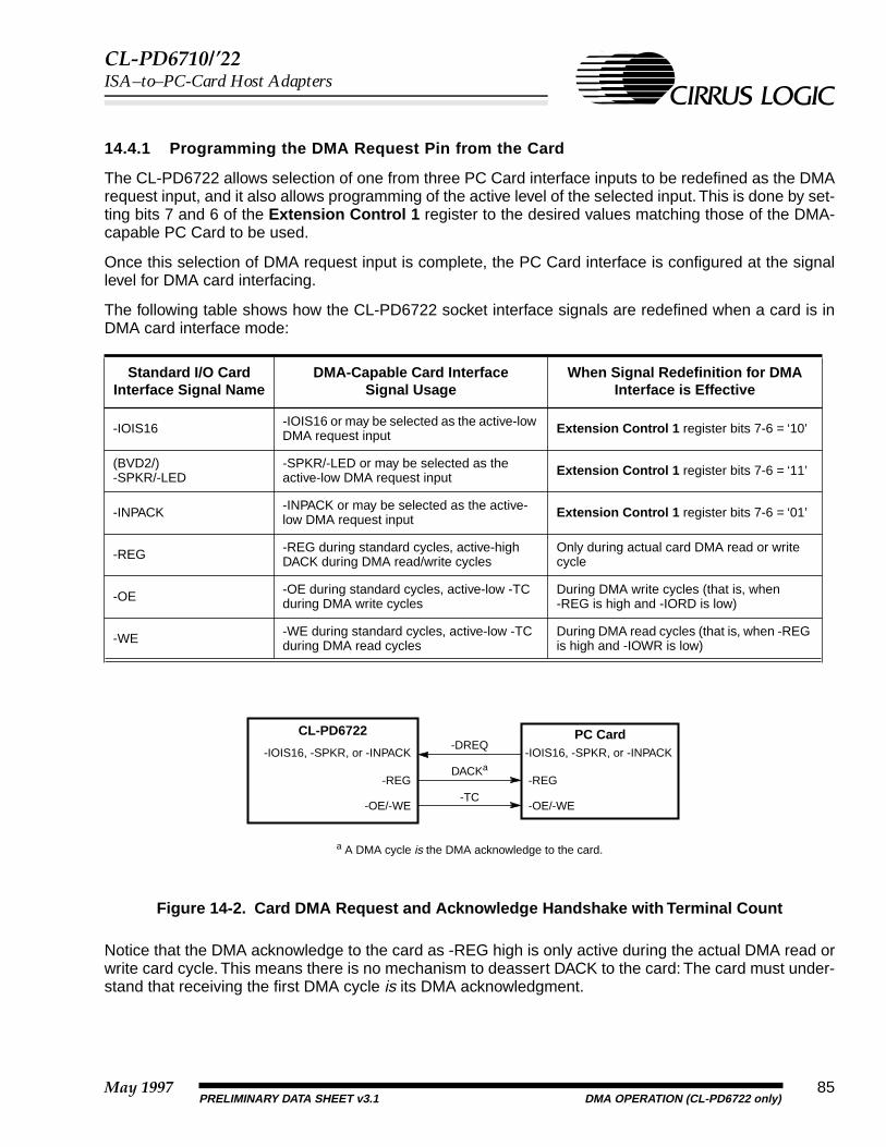
CL-PD6710/’22ISA–to–PC-Card Host Adapters
14.4.1 Programming the DMA Request Pin from the Card
The CL-PD6722 allows selection of one from three PC Card interface inputs to be redefined as the DMArequest input, and it also allows programming of the active level of the selected input. This is done by set-ting bits 7 and 6 of the Extension Control 1 register to the desired values matching those of the DMA-capable PC Card to be used.
Once this selection of DMA request input is complete, the PC Card interface is configured at the signallevel for DMA card interfacing.
The following table shows how the CL-PD6722 socket interface signals are redefined when a card is inDMA card interface mode:
Figure 14-2. Card DMA Request and Acknowledge Handshake with Terminal Count
Notice that the DMA acknowledge to the card as -REG high is only active during the actual DMA read orwrite card cycle. This means there is no mechanism to deassert DACK to the card: The card must under-stand that receiving the first DMA cycle is its DMA acknowledgment.
Standard I/O Card Interface Signal Name
DMA-Capable Card Interface Signal Usage
When Signal Redefinition for DMA Interface is Effective
-IOIS16 -IOIS16 or may be selected as the active-low DMA request input Extension Control 1 register bits 7-6 = ‘10’
(BVD2/)-SPKR/-LED
-SPKR/-LED or may be selected as the active-low DMA request input Extension Control 1 register bits 7-6 = ‘11’
-INPACK -INPACK or may be selected as the active-low DMA request input Extension Control 1 register bits 7-6 = ‘01’
-REG -REG during standard cycles, active-high DACK during DMA read/write cycles
Only during actual card DMA read or write cycle
-OE -OE during standard cycles, active-low -TC during DMA write cycles
During DMA write cycles (that is, when -REG is high and -IORD is low)
-WE -WE during standard cycles, active-low -TC during DMA read cycles
During DMA read cycles (that is, when -REG is high and -IOWR is low)
-DREQ
DACKa
PC CardCL-PD6722
-REG
-IOIS16, -SPKR, or -INPACK-IOIS16, -SPKR, or -INPACK
-REG
a A DMA cycle is the DMA acknowledge to the card.
-TC-OE/-WE-OE/-WE
May 1997 85PRELIMINARY DATA SHEET v3.1 DMA OPERATION (CL-PD6722 only)

CL-PD6710/’22ISA–to–PC-Card Host Adapters
14.4.2 Configuring the Socket Interface for I/O
For DMA support, bit 5 of the Interrupt and General Control register must be set to ‘1’ to put the cardinterface in I/O Card Interface mode.
14.4.3 Preventing Dual Interpretation of DMA Handshake Signals
If the WP/-IOIS16 pin is being used as the DMA request line, the following should be considered:
1) Bit 4 of the Interface Status register is now the level of the DMA request line from the card.
2) Bit 5 of the socket’s two I/O Window Control registers should be set to ‘0’.
If a socket’s BVD2/-SPKR pin is being used as the DMA request line, speaker or LED output from thatsocket is not available.
If -INPACK is selected as the DMA request input, then bit 7 of the Misc Control 1 register should be setto ‘0’ to disable use of this signal as input acknowledge control.
No other register bits require special settings to accommodate DMA support on a socket interface.
14.4.4 Turning On DMA System
The DMA System bit (bit 6 of the Misc Control 2 register) should be programmed to ‘1’ to allow DMAoperation and to redefine ISA bus interface pins for DMA support as in Figure 14-1.
14.5 The DMA Transfer Process
As soon as the selected DMA request input from the card becomes active (low) and the FIFO empties,IRQ10 becomes active (high), signifying a DMA request to the system. The system then responds withan active (low) -DACK at IRQ9, which enables the CL-PD6722 to decode any ISA bus DMA transfers thatmay occur and perform the corresponding transfers at the card. Normal card I/O or memory reads orwrites may be interspersed with DMA read and write cycles.
14.6 Terminal Count to Card at Conclusion of Transfer
At the conclusion of each transfer process, systems send active (high) TC (terminal count) pulses to the-VPP_VALID pin during the last DMA cycles to the CL-PD6722.
For a DMA write cycle, TC active is signaled at the socket interface as the -OE pin going low during DMA-type read cycles from the PC Card.
For a DMA read cycle, TC active is signaled as the -WE pin going low during DMA-type write cycles tothe PC Card.
PRELIMINARY DATA SHEET v3.1May 199786
DMA OPERATION (CL-PD6722 only)

CL-PD6710/’22ISA–to–PC-Card Host Adapters
15. ELECTRICAL SPECIFICATIONS
15.1 Absolute Maximum Ratings
CAUTION: Stresses above those listed may cause permanent damage to system components. These are stressratings only; functional operation at these or any conditions above those indicated in the operationalsections of this specification is not implied. Exposure to absolute maximum rating conditions forextended periods may affect system reliability.
15.2 DC Specifications
Ambient temperature under bias 0°C to 70°CStorage temperature −65°C to 150°C
Voltage on any pin (with respect to ground) −0.5 volts to 0.5 volts greater than voltage of +5V pin, respective to ground
Operating power dissipation 500 mWSuspend power dissipation 10 mWPower supply voltage 7 voltsInjection current (latch up) 25 mA
Table 15-1. General DC Specifications
Symbol Parameter MIN MAX Unit Conditions
CIN Input Capacitance 10.0 pF
COUT Output Capacitance 10.0 pF
IIL Input Leakage −10.0 10.0 µA 0 < VIN < respective VCC supply pin
IPU Internal Pull-up Current −30 −400 µA
May 1997 87PRELIMINARY DATA SHEET v3.1 ELECTRICAL SPECIFICATIONS

CL-PD6710/’22ISA–to–PC-Card Host Adapters
Table 15-2. PC Card Bus Interface DC Specifications
Symbol Parameter MIN MAX Unit Conditions
SOCKET_VCC5V Power Supply Voltage 4.5 5.5 VNormal operation
SOCKET_VCC3V Power Supply Voltage 3.0 3.6 V
VIH Input High Voltage
2.0 V CORE_VDD = 3.0 V, Misc Control 2 register, bit 3 is ‘0’
2.0 V CORE_VDD = 4.5 V, Misc Control 2 register, bit 3 is ‘1’
VIL Input Low Voltage
0.8 V CORE_VDD = 3.6 V, Misc Control 2 register, bit 3 is ‘0’
0.8 V CORE_VDD = 5.5 V, Misc Control 2 register, bit 3 is ‘1’
VIHC Input High Voltage CMOS 0.7 VDD V CORE_VDD = 4.5 V, Misc Control 2 register, bit 3 is ‘0’
VILC Input Low Voltage CMOS 0.2 VDD V CORE_VDD = 5.5 V, Misc Control 2 register, bit 3 is ‘0’
VOH Output High Voltage 2.4 V At rated IOH, respective SOCKET_VCC = 3.0 V
VOHC Output High Voltage CMOS SOCKET_VCC – 0.5 V At rated IOHC,
respective SOCKET_VCC = 3.0 V
VOL Output Low Voltage 0.5 V At rated IOL
IOH Output High Current −2 mARespective SOCKET_VCC = 3.0 V, VOH = 2.4V
IOHC Output High Current CMOS −1 mARespective SOCKET_VCC = 3.0 V, VOHC = SOCKET_VCC – 0.5 V
IOL Output Low Current 2 mARespective SOCKET_VCC = 3.0 V, VOL = 0.5 V
PRELIMINARY DATA SHEET v3.1May 199788
ELECTRICAL SPECIFICATIONS

CL-PD6710/’22ISA–to–PC-Card Host Adapters
a When the CORE_VDD voltage is 3.3 V, input thresholds are TTL compatible; when the CORE_VDD voltage is 5 V, input thresholds are CMOS compatible.
b The value of the input threshold level is dependent on the voltage applied to VDD pins of the CL-PD67XX.
Table 15-3. ISA Bus Interface DC Specifications
Symbol Parameter MIN MAX Unit Conditions
ISA_VCC5V Power Supply Voltage 4.5 5.5 V Normal operation
ISA_VCC3V Power Supply Voltage 3.0 3.6 V Normal operation
VIHa Input High Voltage 2.0 V CORE_VDD = 3.0 V
VILa Input Low Voltage 0.8 V CORE_VDD = 3.6 V
VIHCa Input High Voltage CMOS 0.7 VDD
b V CORE_VDD = 4.5 V
VILCa Input Low Voltage CMOS 0.2 VDD
b V CORE_VDD = 5.5 V
VOH Output High Voltage 2.4 V At rated IOH, ISA_VCC = 3.0 V
VOHC Output High Voltage CMOS ISA_VCC – 0.5 V At rated IOHC, ISA_VCC = 3.0 V
VOL Output Low Voltage 0.5 V At rated IOL
IOH
Output Current High, 2-mA-type driver −2 mA
ISA_VCC = 3.0 V, VOH = 2.4 V
Output Current High, 12-mA-type driver −5 mA
Output Current High, 16-mA-type driver −5 mA
IOHC
Output Current High CMOS, 2-mA-type driver −1 mA
ISA_VCC = 3.0 V, VOHC = ISA_VCC – 0.5 V
Output Current High CMOS, 12-mA-type driver −1 mA
Output Current High CMOS, 16-mA-type driver −1 mA
IOL
Output Current Low, 2-mA-type driver 2 mA
ISA_VCC = 3.0 V, VOL = 0.5 V
Output Current Low, 12-mA-type driver 12 mA
Output Current Low, 16-mA-type driver 16 mA
May 1997 89PRELIMINARY DATA SHEET v3.1 ELECTRICAL SPECIFICATIONS

CL-PD6710/’22ISA–to–PC-Card Host Adapters
a No cards in sockets; for CL-PD6722, bit 5 of the DMA Control register is ‘1’.
Table 15-4. Power Control Interface (+5V Powered) DC Specifications
Symbol Parameter MIN MAX Unit Conditions
+5V +5V Supply Voltage Highest VCC – 0.3 5.5 V
VIH Input High Voltage 2.0 V +5V pin voltage = 4.5 V
VIL Input Low Voltage 0.8 V +5V pin voltage = 5.5 V
VOH Output High Voltage 2.4 V +5V pin voltage = 4.5 V, IOH = −5 mA
VOHC Output High Voltage CMOS +5V volt-age – 0.5 V +5V pin voltage = 4.5 V, IOH = −1 mA
VOL Output Low Voltage 0.5 V
IOHOutput Current High, 16-mA-type driver -5 mA Respective +5V pin voltage = 4.5 V,
VOH = 2.4 V
IOHCOutput Current High CMOS, 16-mA-type driver −1 mA Respective +5V pin voltage = 4.5 V,
VOHC = +5V pin voltage – 0.5 V
IOLOutput Current Low, 16-mA-type driver 16 mA Respective +5V pin voltage = 4.5 V,
VOL = 0.5 V
Table 15-5. Operating Current Specifications
Symbol Parameter MIN TYP MAX Unit Conditions
Icctot(1)Power Supply Current, operating < 6 8 < 20 mA
CORE_VDD = 3.3 V; +5V, SOCKET_VCC, and ISA_VCC = 5.0 V; PDISS = < 85 mW
Icctot(2)Power Supply Current, Suspenda < 150 µA
CORE_VDD = 3.3 V; +5V, SOCKET_VCC, and ISA_VCC = 5.0 V; PDISS = < 2 mW
Icctot(3)
Power Supply Current, Super Suspend, No Clocksa
< 20 µA
CORE_VDD = 3.3 V; +5V, SOCKET_VCC, and ISA_VCC = 5.0 V; PDISS = < 1 mW
PRELIMINARY DATA SHEET v3.1May 199790
ELECTRICAL SPECIFICATIONS

CL-PD6710/’22ISA–to–PC-Card Host Adapters
15.3 AC Timing Specifications
This section includes system timing requirements for the CL-PD67XX. Timings are provided in nanosec-onds (ns), at TTL input levels, with the ambient temperature varying from 0°C to 70°C, and VCC varyingfrom 3.0 to 3.6 V or 4.5 to 5.5 V DC. The AT bus speed is 10 MHz unless otherwise noted. Note that anasterisk (*) denotes an active-low signal for the ISA bus interface, and a dash (-) denotes an active-lowsignal for the PC Card socket interface.
Additionally, the following statements are true for all timing information:
● All timings assume a load of 50 pF.
● TTL signals are measured at TTL threshold; CMOS signals are measured at CMOS threshold.
Table 15-6. List of AC Timing Specifications
Title Page Number
Table 15-7. ISA Bus Timing 92
Table 15-8. Reset Timing 94
Table 15-9. Pulse Mode Interrupt Timing 95
Table 15-10. General-Purpose Strobe Timing 96
Table 15-11. Input Clock Specification 97
Table 15-12. Memory Read/Write Timing (Word Access) 99
Table 15-13. Word I/O Read/Write Timing 100
Table 15-14. PC Card Read/Write Timing when System Is 8-Bit 102
Table 15-15. Normal Byte Read/Write Timing 103
Table 15-16. 16-Bit System to 8-Bit I/O Card: Odd Byte Timing 104
Table 15-17. DMA Read Cycle Timing (CL-PD6722 only) 105
Table 15-18. DMA Write Cycle Timing (CL-PD6722 only) 107
Table 15-19. DMA Request Timing (CL-PD6722 only) 109
May 1997 91PRELIMINARY DATA SHEET v3.1 ELECTRICAL SPECIFICATIONS

CL-PD6710/’22ISA–to–PC-Card Host Adapters
15.3.1 ISA Bus Timing
Table 15-7. ISA Bus Timing
Symbol Parameter MIN MAX Unit
t1 MEMCS16* active delay from LA[23:17] valid 40 ns
t1a LA[23:17] setup to ALE inactive 30 ns
t1b LA[23:17] hold from ALE inactive 5 ns
t2 IOCS16* active delay from SA[15:0]1 40 ns
t2a IOCS16* inactive delay from SA[15:0]1 40 ns
t3 SA[16:0], SBHE* setup to any Command active1, 2
LA[23:17] latching by ALE to any Command active3090
nsns
t4 Any Command active to IOCHRDY inactive (low)3 40 ns
t4a IOCHRDY three-state from Command inactive4 5 30
t5 MEMCS16* inactive delay from unlatched LA[23:17] 40 ns
t6a IOW* or IOR* pulse width1 140 ns
t6b MEMW* or MEMR* pulse width1 180 ns
t7 Any Command inactive to next Command active 100 ns
t8 Address or SBHE* hold from any Command inactive 0 ns
t9 Data valid from MEMW* active5
Data valid from IOW* active4040
nsns
t10 Data hold from MEMW* inactiveData hold from IOW* inactive
55
nsns
t11 Data delay from IOR* active, for internal registers 0 130 ns
t12 Data delay from IOCHRDY active 15 ns
t13 Data hold from IOR* or MEMR* inactive 0 30 ns
t14 AEN inactive setup to valid IOR* or IOW* active 40 ns
t15 AEN hold from IOR* or IOW* inactive 5 ns
t16 REFRESH* inactive setup to valid MEMR* or MEMW* active 40 ns
t17 REFRESH* inactive hold from MEMR* or MEMW* active 0 ns
t18 MEMCS16* active delay from SA[16:12] valid 40 ns
t19 *ZWS delay from MEMW* active 30 ns
t20 *ZWS hold from MEMW* inactive 15 ns
1 AEN must be inactive for t2, t3, and t6 timing specifications to be applicable.2 Command is defined as IOR*, IOW*, MEMR*, or MEMW*.3 Except for valid card memory writes, which are zero wait state when internal write FIFO is not full.4 If card is removed during a card access cycle, IOCHRDY is three-stated without waiting for end of Command.5 Based on 25-MHz internal clock, produced either by an internal synthesizer and 14.318-MHz signal applied to CLK pin,
or by supplying 25 MHz directly to CLK pin and bypassing the internal synthesizer.
PRELIMINARY DATA SHEET v3.1May 199792
ELECTRICAL SPECIFICATIONS

CL-PD6710/’22ISA–to–PC-Card Host Adapters
Figure 15-1. Bus Timing — ISA Bus
LA[23:17]
SA[16:0]SBHE*
MEMCS16*
IOCS16*
MEMR*, MEMW*IOR*, IOW*
IOCHRDY
WRITE DATA
READ DATA
VALID VALID
VALID
t1
t2
t3
t4
t5
t6a, t6bt7
t8
t9 t10
t12
t13
AENt14 t15
REFRESH* t16 t17
t18
ALE
t2a
t1a t1b
t4a
t20t19ZWS*
t11
May 1997 93PRELIMINARY DATA SHEET v3.1 ELECTRICAL SPECIFICATIONS

CL-PD6710/’22ISA–to–PC-Card Host Adapters
15.3.2 Reset Timing
Figure 15-2. Reset Timing
Table 15-8. Reset Timing
Symbol Parameter MIN MAX Units
t1 PWRGOOD generated reset pulse width 500 ns
t2 Clock active before end of reset1 500 ns
t3 End of PWRGOOD generated reset to first Command 500 ns
1 Clock input must be active for a minimum of 500 ns before PWRGOOD goes active to allow sufficient internal clocks to initialize internal circuitry.
t1
MEMR*, MEMW*
t3
PWRGOOD
IOR*, IOW*
CLK
t2
PRELIMINARY DATA SHEET v3.1May 199794
ELECTRICAL SPECIFICATIONS

CL-PD6710/’22ISA–to–PC-Card Host Adapters
15.3.3 System Interrupt Timing
Figure 15-3. Pulse Mode Interrupt Timing
Table 15-9. Pulse Mode Interrupt Timing
Symbol Parameter MIN MAX
t 1 IRQ[XX] low or high 2 CLK – 10 ns 2 CLK + 10 ns
IRQ[XX]High-Z High-Z
t1 t1
High-Z = high impedanceNOTE: Each time indicated is 2 clock periods of the CLK input to the CL-PD67XX, independent of setting of the
Bypass Frequency Synthesizer bit.
May 1997 95PRELIMINARY DATA SHEET v3.1 ELECTRICAL SPECIFICATIONS

CL-PD6710/’22ISA–to–PC-Card Host Adapters
15.3.4 General-Purpose Strobe Timing (CL-PD6722 only)
Figure 15-4. General-Purpose Strobe Timing
Table 15-10.General-Purpose Strobe Timing
Symbol Parameter MIN MAX Units
t1 GPSTB delay after IOR* or IOW* active 40 ns
t2 GPSTB delay after IOR* or IOW* inactive 40 ns
IOR*, IOW*
t1
GPSTB
t2
PRELIMINARY DATA SHEET v3.1May 199796
ELECTRICAL SPECIFICATIONS

CL-PD6710/’22ISA–to–PC-Card Host Adapters
15.3.5 Input Clock Specification
Figure 15-5. Input Clock Specification
Table 15-11.Input Clock Specification
Symbol Parameter MIN MAX Units Conditions
t1 CLK pin input rise time 1 7 ns
t2 CLK pin input fall time 1 7 ns
t3 CLK input low period 0.4 TCLKP 0.6 TCLKP ns
t4 CLK input high period 0.4 TCLKP 0.6 TCLKP ns
Vcenter Center voltage at which period specified
0.5 VDD 0.5 VDD V
TCLKP Input clock period,internal clock
69.84 – 0.1% 69.84 + 0.1% ns Normal synthesizer operation. Misc Control 2 register, bit 0 = ‘0’. CLK pin at 14.318 MHz.
TCLKP Input clock period,external clock
40 – 0.1% 40 + 0.1% ns Synthesizer bypassed. Misc Control 2 register, bit 0 = ‘1’. CLK pin at 25 MHz.
VIHmin CLK input high voltage 2.0 V CORE_VDD = 3.0 V
VILmax CLK input low voltage 0.8 V CORE_VDD = 3.6 V
VIHCmin CLK input high voltage 0.7 VDD V CORE_VDD = 4.5 V
VILCmax CLK input low voltage 0.2 VDD V CORE_VDD = 5.5 V
t1
VILmax, VILCmax
t2
t3 t4
TCLKP
CLK
VIHmin, VIHCmin
Vcenter
May 1997 97PRELIMINARY DATA SHEET v3.1 ELECTRICAL SPECIFICATIONS

CL-PD6710/’22ISA–to–PC-Card Host Adapters
PRELIMINARY DATA SHEET v3.1May 199798
ELECTRICAL SPECIFICATIONS
15.3.6 PC Card Bus Timing Calculations
Calculations for minimum PC Card cycle Setup, Command, and Recovery timings are made by first cal-culating factors derived from the applicable timer set’s timing registers and then by applying the factor toan equation relating it to the internal clock period.
The PC Card cycle timing factors, in terms of the number of internal clocks, are calculated as follows:
S = (Npres × Nval) + 1 Equation 15-1
C = (Npres × Nval) + 1 Equation 15-2
R = (Npres × Nval) + 1 Equation 15-3
Npres and Nval are the specific selected prescaler and multiplier value from the timer set’s Setup, Com-mand, and Recovery Timing registers (see Chapter 10 for a description of these registers).
From this, a PC Card cycle’s Setup, Command, and Recovery time for the selected timer set are calcu-lated as follows:
Setup time = (S × Tcp) ± 10 ns Equation 15-4
Command time = (C × Tcp) ± 10 ns Equation 15-5
Recovery time = (R × Tcp) ± 10 ns Equation 15-6
When the internal synthesizer is used, the calculation of the internal clock period Tcp is:
Tcp = TCLKP × 4/7 Equation 15-7
where TCLKP is the period of the clock supplied to the CLK input pin. An input frequency of 14.318 MHzat the CLK input pin results in an internal clock period of Tcp = 40 ns.
When the internal synthesizer is bypassed, Tcp = TCLKP. An input frequency of 25 MHz in this circum-stance would also result in an internal clock period of Tcp = 40 ns.
The timing diagrams that follow were derived for a CL-PD67XX using the internal synthesizer and a14.318-MHz CLK pin input. The internal clock frequency of the CL-PD67XX is 7/4 of this incoming signal(Tcp = 40 ns). The examples are for the default values of the Timing registers for Timer Set 0, as follows:
Thus the minimum times for the default values are as follows:
Default minimum Setup time = (S × Tcp) – 10 ns = {2 × 40 ns} – 10 ns = 70 ns Equation 15-8
Timing Register Name(Timer Set 0)
IndexValue
(Default)Resultant
Npres
Resultant Nval
Setup Timing 0 3Ah 01h 1 1
Command Timing 0 3Bh 06h 1 6
Recovery Timing 0 3Ch 03h 1 3

CL-PD6710/’22ISA–to–PC-Card Host Adapters
May 1997 99PRELIMINARY DATA SHEET v3.1 ELECTRICAL SPECIFICATIONS
Default minimum Command time = (C × Tcp) – 10 ns = {7 × 40 ns} – 10 ns = 270 ns Equation 15-9
Default minimum Recovery time = (R × Tcp) – 10 ns = {4 × 40 ns} – 10 ns = 150 ns Equation 15-10
15.3.7 PC Card Socket Timing
Table 15-12. Memory Read/Write Timing (Word Access)
Symbol Parameter MIN MAX Units
t1-CE[2:1], -REG, Address, and Write Data setup to Command active1 (S × Tcp) – 10 ns
t2 Command pulse width2 (C × Tcp) – 10 ns
t3 Address hold and Write Data valid from Command inactive3 (R × Tcp) – 10 ns
t4 -WAIT active from Command active4 (C – 2)Tcp – 10 ns
t5 Command hold from -WAIT inactive (2 Tcp) + 10 ns
t6 Data valid from -WAIT inactive Tcp + 10 ns
t7 Data setup before -OE inactive (2 Tcp) + 10 ns
t8 Data hold after -OE inactive 0 ns
1 The Setup time is determined by the value programmed into the Setup Timing register, index 3Ah/3Dh. Using the Timer Set 0 default value of 01h, the setup time would be 70 ns. S = (Npres × Nval + 1), see page 98.
2 The Command time is determined by the value programmed into the Command Timing register, index 3Bh/3Eh. Using the Timer Set 0 default value of 06h, the Command time would be 270 ns. C = (Npres × Nval + 1), see page 98.
3 The Recovery time is determined by the value programmed into the Recovery Timing register, index 3Ch/3Fh. Using the Timer Set 0 default value of 03h, the hold (Recovery) time would be 150 ns. R = (Npres × Nval + 1), see page 98.
4 For typical active timing programmed at 280 ns, maximum -WAIT timing is 190 ns after Command active.
-REG, -CE[2:1],
t1t2
t4
t3
-WAIT
t7
D[15:0]
D[15:0]
t8
t5
A[25:0]
-OE, -WE
t6
Write Cycle
Read Cycle

CL-PD6710/’22ISA–to–PC-Card Host Adapters
PRELIMINARY DATA SHEET v3.1May 1997100
ELECTRICAL SPECIFICATIONS
Figure 15-6. Memory Read/Write Timing
Table 15-13. Word I/O Read/Write Timing
Symbol Parameter MIN MAX Units
t1 -REG or Address setup to Command active1 (S × Tcp) – 10 ns
t2 Command pulse width2 (C × Tcp) – 10 ns
t3 Address hold and Write Data valid from Command inactive3 (R × Tcp) – 10 ns
t4 -WAIT active from Command active4 (C – 2)Tcp – 10 ns
t5 Command hold from -WAIT inactive (2 Tcp) + 10 ns
tref Card -IOIS16 delay from valid Address (PC Card specification) 35 ns
t6 -IOIS16 setup time before Command end (3 Tcp) + 10 ns
t7 -CE2 delay from -IOIS16 active5 Tcp – 10 ns
t6 Data valid from -WAIT inactive Tcp + 10 ns
t9 Data setup before -IORD inactive (2 Tcp) + 10 ns
t10 Data hold after -IORD inactive 0 ns
1 The Setup time is determined by the value programmed into the Setup Timing register, index 3Ah/3Dh. Using the Timer Set 0 default value of 01h, the setup time would be 70 ns. S = (Npres × Nval + 1), see page 98.
2 The Command time is determined by the value programmed into the Command Timing register, index 3Bh/3Eh. Using the Timer Set 0 default value of 06h, the Command time would be 270 ns. C = (Npres × Nval + 1), see page 98.
3 The Recovery time is determined by the value programmed into the Recovery Timing register, index 3Ch/3Fh. Using the Timer Set 0 default value of 03h, the hold (Recovery) time would be 150 ns. R = (Npres × Nval + 1), see page 98.
4 For typical active timing programmed at 280 ns, maximum -WAIT timing is 190 ns after Command active.5 -IOIS16 must go low within 3Tcp + 10 ns of the cycle beginning or -IOIS16 will be ignored and -CE will not be activated.

CL-PD6710/’22ISA–to–PC-Card Host Adapters
May 1997 101PRELIMINARY DATA SHEET v3.1 ELECTRICAL SPECIFICATIONS
Figure 15-7. Word I/O Read/Write Timing
-IOWR, -IORD
t1t2
t6
t3
-IOIS16
t7
-CE1
-REG,A[25:0]
-CE2
D[15:0]
tref
Write Cycle
t4
-WAIT
t5
t9
D[15:0]
t10t8
Read Cycle

CL-PD6710/’22ISA–to–PC-Card Host Adapters
Figure 15-8. PC Card Read/Write Timing When System Is 8-Bit(SBHE Tied High)
Table 15-14. PC Card Read/Write Timing when System Is 8-Bit
Symbol Parameter MIN MAX Units
t1 -REG or Address setup to Command active1 (S × Tcp) – 10 ns
t2 Command pulse width2 (C × Tcp) – 10 ns
t3 Address hold from Command inactive3 (R × Tcp) – 10 ns
t4 Data setup before Command inactive (2 Tcp) + 10 ns
t5 Data hold after command inactive 0 ns
1 The Setup time is determined by the value programmed into the Setup Timing register, index 3Ah/3Dh. Using the Timer Set 0 default value of 01h, the setup time would be 70 ns. S = (Npres × Nval + 1), see page 98.
2 The Command time is determined by the value programmed into the Command Timing register, index 3Bh/3Eh. Using the Timer Set 0 default value of 06h, the Command time would be 270 ns. C = (Npres × Nval + 1), see page 98.
3 The Recovery time is determined by the value programmed into the Recovery Timing register, index 3Ch/3Fh. Using the Timer Set 0 default value of 03h, the hold (Recovery) time would be 150 ns. R = (Npres × Nval + 1), see page 98.
-IOWR, -IORD,
t1t2
t3
-CE1
-REG,
A[25:0]
D[7:0]Odd/even Data
D[15:8]XX
-OE, -WE
D[7:0]
Read Cycle
t5t4
Write Cycle
Read orWrite Cycle
Odd/Even Data
PRELIMINARY DATA SHEET v3.1May 1997102
ELECTRICAL SPECIFICATIONS

CL-PD6710/’22ISA–to–PC-Card Host Adapters
May 1997 103
Figure 15-9. Normal Byte Read/Write Timing
Table 15-15. Normal Byte Read/Write Timing
Symbol Parameter MIN MAX Units
t1 Address setup to Command active1 (S × Tcp) – 10 ns
t2 Command pulse width2 (C × Tcp) – 10 ns
t3 Address hold from Command inactive3 (R × Tcp) – 10 ns
1 The Setup time is determined by the value programmed into the Setup Timing register, index 3Ah/3Dh. Using the Timer Set 0 default value of 01h, the setup time would be 70 ns. S = (Npres × Nval + 1), see page 98.
2 The Command time is determined by the value programmed into the Command Timing register, index 3Bh/3Eh. Using the Timer Set 0 default value of 06h, the Command time would be 270 ns. C = (Npres × Nval + 1), see page 98.
3 The Recovery time is determined by the value programmed into the Recovery Timing register, index 3Ch/3Fh. Using the Timer Set 0 default value of 03h, the hold (Recovery) time would be 150 ns. R = (Npres × Nval + 1), see page 98.
-REG,
-IOWR, -IORD,
t1t2
t3
-CE1
A[25:0]
-CE2
D[7:0] Odd/Even Data
D[15:8]XX
-OE, -WE
Write Cycle
Read orWrite Cycle
D[7:0]Read Cycle
Odd/Even Data
NOTE: Figure 15-9 applies to all other byte accesses, including odd I/O cycleswhere -IOIS16 is low.
PRELIMINARY DATA SHEET v3.1 ELECTRICAL SPECIFICATIONS

CL-PD6710/’22ISA–to–PC-Card Host Adapters
Figure 15-10. 16-Bit System to 8-Bit I/O Card: Odd Byte Timing
Table 15-16.16-Bit System to 8-Bit I/O Card: Odd Byte Timing
Symbol Parameter MIN MAX Units
t1 Address change to -IOIS16 inactive4 (3Tcp) + 10 ns
t2 -IOIS16 inactive to -CE2 inactive 20 ns
t3 -IOIS16 inactive to -CE1 active 20 ns
t4 Address setup to Command active1 (S × Tcp) – 10 ns
t5 Command pulse width2 (C × Tcp) – 10 ns
t6 Address hold from Command inactive3 (R × Tcp) – 10 ns
1 The Setup time is determined by the value programmed into the Setup Timing register, index 3Ah/3Dh. Using the Timer Set 0 default value of 01h, the setup time would be 70 ns. S = (Npres × Nval + 1), see page 98.
2 The Command time is determined by the value programmed into the Command Timing register, index 3Bh/3Eh. Using the Timer Set 0 default value of 06h, the Command time would be 270 ns. C = (Npres × Nval + 1), see page 98.
3 The Recovery time is determined by the value programmed into the Recovery Timing register, index 3Ch/3Fh. Using the Timer Set 0 default value of 03h, the hold (Recovery) time would be 150 ns. R = (Npres × Nval + 1), see page 98.
4 -IOIS16 level from card should be valid before -IOWR/-IORD goes active. For a typical setup time of 70 ns, a PC Card meeting the PCMCIA specification for -IOIS16 from A[25:0] change will meet this condition.
-REG,
-IOIS16
t3
-CE1
A[25:0]
-CE2
D[7:0]Odd Data
t2
Write Cycle
D[7:0]Read Cycle
Odd Data
D[15:8]XXRead or
Write Cycle
-IOWR, -IORD
t4t5
t6
t1
PRELIMINARY DATA SHEET v3.1May 1997104
ELECTRICAL SPECIFICATIONS

CL-PD6710/’22ISA–to–PC-Card Host Adapters
Table 15-17. DMA Read Cycle Timing (CL-PD6722 only)
Symbol Parameter MIN MAX Units
t1 DRQ (IRQ10) and DACK* (IRQ9) active to DMA cycle begin 40 ns
t2 -CE[2:1], -REG, -IORD, -OE, and Write Data setup to -IOWR active1
(S × Tcp) – 10 ns
t3 Command: -IOWR pulse width2 (C × Tcp) – 10 ns
t4 Recovery: -IOWR inactive to end of cycle3 (R × Tcp) – 10 ns
t5 -WAIT active from -IOWR active (C – 2)Tcp – 10 ns
t6 -WAIT inactive to -IOWR inactive 2 Tcp ns
t7 System TC (-VPP_VALID high) to -IOWR −40 ns
t8 -IOWR to begin of card TC (-WE)4 25 50 ns
t9 End of card TC (-WE) to -IOWR inactive4 25 50 ns
1 The Setup time is determined by the value programmed into the Setup Timing register, index 3Ah/3Dh. Using the Timer Set 0 default value of 01h, the setup time would be 70 ns. S = (Npres × Nval + 1), see page 98.
2 The Command time is determined by the value programmed into the Command Timing register, index 3Bh/3Eh. Using the Timer Set 0 default value of 06h, the Command time would be 270 ns. C = (Npres × Nval + 1), see page 98.
3 The Recovery time is determined by the value programmed into the Recovery Timing register, index 3Ch/3Fh. Using the Timer Set 0 default value of 03h, the hold (Recovery) time would be 150 ns. R = (Npres × Nval + 1), see page 98.
4 Based on an internal clock period of 40 ns (25 MHz).
May 1997 105PRELIMINARY DATA SHEET v3.1 ELECTRICAL SPECIFICATIONS

CL-PD6710/’22ISA–to–PC-Card Host Adapters
PRELIMINARY DATA SHEET v3.1May 1997106
ELECTRICAL SPECIFICATIONS
Figure 15-11. DMA Read Cycle Timing
-CE[2:1]
t2t3
t5
t4
-WAIT
DMA DATA[15:0]
-VPP_VALID
t6
-IOWR
to card
(TC from system)
IRQ9
-IORD, -OE
-REG
(DACK*)
(high)
(DACK* to card)
t1
t7
-WE(TC to card)
t8 t9
IRQ10(DRQ)

CL-PD6710/’22ISA–to–PC-Card Host Adapters
May 1997 107
Table 15-18. DMA Write Cycle Timing (CL-PD6722 only)
Symbol Parameter MIN MAX Units
t1 DRQ (IRQ10) and DACK* (IRQ9) active to DMA cycle begin 40 ns
t2 -CE[2:1], -REG, -IOWR, -WE, and Write Data setup to -IORD active1
(S × Tcp) – 10 ns
t3 Command: -IORD pulse width2 (C × Tcp) – 10 ns
t4 Recovery: -IORD inactive to end of cycle3 (R × Tcp) – 10 ns
t5 -WAIT active from -IORD active (C – 2)Tcp – 10 ns
t6 -WAIT inactive to -IORD inactive 2 Tcp ns
t7 System TC (-VPP_VALID high) to -IORD −40 ns
t8 -IORD to begin of card TC (-OE)4 25 50 ns
t9 End of card TC (-OE) to -IORD inactive4 25 50 ns
t10 Data valid from -WAIT inactive Tcp + 10 ns
t11 Data setup before -OE inactive (2 Tcp) +10 ns
t12 Data hold after -OE inactive 0 ns
1 The Setup time is determined by the value programmed into the Setup Timing register, index 3Ah/3Dh. Using the Timer Set 0 default value of 01h, the setup time would be 70 ns. S = (Npres × Nval + 1), see page 98.
2 The Command time is determined by the value programmed into the Command Timing register, index 3Bh/3Eh. Using the Timer Set 0 default value of 06h, the Command time would be 270 ns. C = (Npres × Nval + 1), see page 98.
3 The Recovery time is determined by the value programmed into the Recovery Timing register, index 3Ch/3Fh. Using the Timer Set 0 default value of 03h, the hold (Recovery) time would be 150 ns. R = (Npres × Nval + 1), see page 98.
4 Based on an internal clock period of 40 ns (25 MHz).
PRELIMINARY DATA SHEET v3.1 ELECTRICAL SPECIFICATIONS

CL-PD6710/’22ISA–to–PC-Card Host Adapters
PRELIMINARY DATA SHEET v3.1May 1997108
ELECTRICAL SPECIFICATIONS
Figure 15-12. DMA Write Cycle Timing
-CE[2:1]
t2t3
t5
t4
-WAIT
DMA DATA[15:0]
-VPP_VALID
t6
-IORD
to card
(TC from system)
IRQ9
-IOWR, -WE
-REG
(DACK*)
(high)
(DACK* to card)
t1
-OE(TC to card)
t11
DMA DATA[15:0]
t12t10
from card
t7
t8 t9
IRQ10(DRQ)

CL-PD6710/’22ISA–to–PC-Card Host Adapters
May 1997 109PRELIMINARY DATA SHEET v3.1 ELECTRICAL SPECIFICATIONS
Figure 15-13. DMA Request Timing
Table 15-19. DMA Request Timing (CL-PD6722 only)
Symbol Parameter MIN MAX Units
t1 DMA request from socket interface to system1 40 ns
1 After FIFO empty, DMA requests held off from being presented to the system until all write data to a card has been emp-tied from the socket interface FIFO.
-INPACK, WP/-IOIS16,
t1
or BVD2/-SPKR 2
(-DREQ from card)
IRQ10(DRQ to system)
2 DMA Control register bits 7 and 6 define which of these three signals serve as the active-low DMA request from the card.

CL-PD6710/’22ISA–to–PC-Card Host Adapters
16. PACKAGE SPECIFICATIONS
16.1 144-Pin VQFP Package
NOTES:
1) Dimensions are in millimeters (inches), and controlling dimension is millimeter.
2) Before beginning any new design with this device, please contact Cirrus Logic for the latest package information.
Pin 1 Indicator
17.50 (0.689) REF
Pin 1
21.60 (0.850)22.40 (0.882)
0.10 (0.004)0.30 (0.012)
19.90 (0.783)20.10 (0.791)
17.50(0.689)
REF0.50
(0.0197)BSC
1.25 (0.049)1.50 (0.059)
0° MIN7° MAX
0.10 (0.004)0.20 (0.008)
1.40 (0.055)1.65 (0.065)
0.45 (0.018)0.75 (0.030)
21.60 (0.850)22.40 (0.882)
19.90 (0.783)20.10 (0.791)
1.00(0.039)
REF
0.05 (0.002)0.15 (0.006)
Pin 144
144-Pin VQFP
CL-PD6710
PRELIMINARY DATA SHEET v3.1May 1997110
PACKAGE SPECIFICATIONS

CL-PD6710/’22ISA–to–PC-Card Host Adapters
16.2 208-Pin PQFP Package
NOTES:
1) Dimensions are in millimeters (inches), and controlling dimension is inches.
2) Drawing above does not reflect exact package pin count.
3) Before beginning any new design with this device, please contact Cirrus Logic for the latest package information.
Pin 1 Indicator
25.50 (1.004) REF
30.35 (1.195)30.85 (1.215)
0.13 (0.005)0.28 (0.011)
27.90 (1.098)28.10 (1.106)
25.50(1.004)
REF
0.50(0.0197)
BSC
30.35 (1.195)30.85 (1.215)
27.90 (1.098)28.10 (1.106)
3.17 (0.125)3.67 (0.144)
0° MIN7° MAX
0.09 (0.004)0.23 (0.009)
4.07 (0.160) MAX
0.40 (0.016)0.75 (0.030)
0.25 (0.010) MIN
1.30 (0.051) REF
Pin 1
Pin 208
208-Pin PQFP
CL-PD6722
May 1997 111PRELIMINARY DATA SHEET v3.1 PACKAGE SPECIFICATIONS

CL-PD6710/’22ISA–to–PC-Card Host Adapters
16.3 208-Pin VQFP Package
NOTES:
1) Dimensions are in millimeters (inches), and controlling dimension is inches.
2) Drawing above does not reflect exact package pin count.
3) Before beginning any new design with this device, please contact Cirrus Logic for the latest package information.
208-Pin VQFPCL-PD6722
Pin 1 Indicator
29.60 (1.165)30.40 (1.197)
0.17 (0.007)0.27 (0.011)
27.80 (1.094)28.20 (1.110)
0.50(0.0197)
BSC
29.60 (1.165)30.40 (1.197)
27.80 (1.094)28.20 (1.110)
1.35 (0.053)1.45 (0.057)
0° MIN7° MAX
0.09 (0.004)0.20 (0.008)
1.40 (0.055)
0.45 (0.018)0.75 (0.030)
0.05 (0.002)
1.00 (0.039) BSC
Pin 1
Pin 208
1.60 (0.063) 0.15 (0.006)
PRELIMINARY DATA SHEET v3.1May 1997112
PACKAGE SPECIFICATIONS

CL-PD6710/’22ISA–to–PC-Card Host Adapters
17. ORDERING INFORMATION EXAMPLE
The order number for the part is:
CL – PD67XX – QC – ACirrus Logic, Inc.
Product Line:
Part Number Package Type:
Temperature Range:
Revision †
C = Commercial
Q = Plastic Quad Flat Pack (CL-PD6722)
† Contact Cirrus Logic for up-to-date information on revisions.
Portable Products
V = Very-tight-pitch Quad Flat Pack
May 1997 113PRELIMINARY DATA SHEET v3.1 ORDERING INFORMATION EXAMPLE

CL-PD6710/’22ISA–to–PC-Card Host Adapters
Appendix A
A.Using the Cirrus Logic BBS and FTP Server
Using the Cirrus Logic BBS
Cirrus Logic maintains a BBS (bulletin board system) 24 hours a day for customers to obtain up-to-datefiles and information. For the CL-PD67XX, the BBS gives access to utilities, schematics, and softwareupgrades.
Cirrus Logic strictly controls access to this BBS. All downloadable files are checked by Cirrus Logic andcustomers cannot upload files to any publicly downloadable area.
Follow the steps that follow to download files. If you would like access to more restricted files, or wouldlike to exchange files with Cirrus Logic personnel on a regular basis, contact your Cirrus Logic represen-tative to obtain expanded access privileges.
1. Set your communication parameters as follows:
● 8 data bits
● No parity
● 1 stop bit
● Baud rate up to 14,400 bps
2. Dial the Cirrus Logic BBS at (510) 440-9080.
3. When connected, do one of the following:
● Enter your name and password. First-time users can establish an account by entering a name and passwordand completing the questionnaire.
● Or, follow the instructions to log on as a ‘guest’.
4. Select [J] Join Product Area.
5. Select [19] 67XX.
6. Select [F] File Menu.
7. You can now choose among the options.
Many BBS files are compressed in a ‘zipped’ file format (using PKZIP.EXE version 2.04G). These files have thesuffix .ZIP appended to their names. They need to be uncompressed after downloading using PKUNZIP.EXE. Ifyou do not have this ‘unzip’ utility, you can download it in a self-extracting form from the Cirrus Logic BBS —from any area, download the file called PKZ204G.EXE.
PRELIMINARY DATA SHEET v3.1May 1997114

CL-PD6710/’22ISA–to–PC-Card Host Adapters
Using the FTP Server
In addition to the BBS, Cirrus Logic maintains an anonymous FTP site on the internet. The address isftp.cirrus.com. Using any password, you can log on as anonymous or FTP.
You can also access this site using a World-Wide Web browser by linking from the Cirrus Logic home pageat the address http://www.cirrus.com/.
NOTE: The FTP server is limited to released software drivers. BIOS, schematics, and beta software is available onlyon the BBS and is restricted to licensed OEMs.
When you log into the FTP site, you will be in the FTP directory. Change directories to /pub/support.This the main directory of the FTP site.
In the support directory, a document named ftp_contents.doc shows the FTP file names and theircontents. Like the BBS, the FTP site is arranged by chip set. The support directory provides access tothe desktop, laptop, modem, PCMCIA, and SIO areas. Within these directories are the chip-set subdirec-tories. Within these subdirectories are software files.
May 1997 115PRELIMINARY DATA SHEET v3.1

CL-PD6710/’22ISA–to–PC-Card Host Adapters
Appendix B
B.Register Summary Tables
B.1 Operation Registers
B.2 Chip Control Registers
a Value for the current stepping only.
Register Name: IndexIndex: n/a
Register Per: chipRegister Compatibility Type: 365
Bit 7 Bit 6 Bit 5 Bit 4 Bit 3 Bit 2 Bit 1 Bit 0
Device Index Socket Index Register Index
RW:0 RW:0 RW:000000
Register Name: DataIndex: n/a
Register Per: chipRegister Compatibility Type: 365
Bit 7 Bit 6 Bit 5 Bit 4 Bit 3 Bit 2 Bit 1 Bit 0
Data
Register Name: Chip RevisionIndex: 00h
Register Per: chipRegister Compatibility Type: 365
Bit 7 Bit 6 Bit 5 Bit 4 Bit 3 Bit 2 Bit 1 Bit 0
Interface ID 0 0 Revision
R:10 R:0 R:0 R:0010a
Register Name: Interface StatusIndex: 01h
Register Per: socketRegister Compatibility Type: 365
Bit 7 Bit 6 Bit 5 Bit 4 Bit 3 Bit 2 Bit 1 Bit 0-VPP_VALID RDY WP -CD2 -CD1 BVD2 BVD1
VPP Valid Card Power On Ready/Busy* Write Protect Card Detect Battery Voltage Detect
Ra R:0 Rb Rc Rd Re
PRELIMINARY DATA SHEET v3.1May 1997116

CL-PD6710/’22ISA–to–PC-Card Host Adapters
a Bit 7 is the inversion of the value of the -VPP_VALID pin (see page 15).b Bit 5 is the value of the RDY/-IREQ pin (see page 17).c Bit 4 is the value of the WP/-IOIS16 pin (see page 17).d Bits 3:2 are the inversion of the values of the -CD1 and -CD2 pins (see page 18).e Bits 1:0 are the values of the BVD1/-STSCHG and BVD2/-SPKR pins (see page 18).
Register Name: Power ControlIndex: 02h
Register Per: socketRegister Compatibility Type: 365
Bit 7 Bit 6 Bit 5 Bit 4 Bit 3 Bit 2 Bit 1 Bit 0
Card Enable Compatibility Bit Auto-Power VCC Power Compatibility Bits VPP1 Power
RW:0 RW:0 RW:0 RW:0 RW:00 RW:00
Register Name: Interrupt and General ControlIndex: 03h
Register Per: socketRegister Compatibility Type: 365
Bit 7 Bit 6 Bit 5 Bit 4 Bit 3 Bit 2 Bit 1 Bit 0
Ring Indicate Enable Card Reset* Card Is I/O
Enable Management
InterruptsCard IRQ Select
RW:0 RW:0 RW:0 RW:0 RW:0000
Register Name: Card Status ChangeIndex: 04h
Register Per: socketRegister Compatibility Type: 365
Bit 7 Bit 6 Bit 5 Bit 4 Bit 3 Bit 2 Bit 1 Bit 0
0 0 0 0 Card Detect Change
Ready Change
Battery Warning Change
Battery Dead Or Status Change
R:0 R:0 R:0 R:0 R:0 R:0 R:0 R:0
Register Name: Management Interrupt ConfigurationIndex: 05h
Register Per: socketRegister Compatibility Type: 365
Bit 7 Bit 6 Bit 5 Bit 4 Bit 3 Bit 2 Bit 1 Bit 0
Management IRQ Select Card Detect Enable Ready Enable
Battery Warning Enable
Battery Dead Or Status Change Enable
RW:0000 RW:0 RW:0 RW:0 RW:0
Register Name: Mapping EnableIndex: 06h
Register Per: socketRegister Compatibility Type: 365
Bit 7 Bit 6 Bit 5 Bit 4 Bit 3 Bit 2 Bit 1 Bit 0
I/O Map 1 Enable
I/O Map 0 Enable
MEMCS16 Full Decode
Memory Map 4 Enable
Memory Map 3 Enable
Memory Map 2 Enable
Memory Map 1 Enable
Memory Map 0 Enable
RW:0 RW:0 RW:0 RW:0 RW:0 RW:0 RW:0 RW:0
May 1997 117PRELIMINARY DATA SHEET v3.1

CL-PD6710/’22ISA–to–PC-Card Host Adapters
B.3 I/O Window Mapping Registers
Register Name: I/O Window ControlIndex: 07h
Register Per: socketRegister Compatibility Type: 365
Bit 7 Bit 6 Bit 5 Bit 4 Bit 3 Bit 2 Bit 1 Bit 0
Timing Register Select 1
Compatibility Bit
Auto-Size I/O Window 1
I/O Window 1 Size
Timing Register Select 0
Compatibility Bit
Auto-Size I/O Window 0
I/O Window 0 Size
RW:0 RW:0 RW:0 RW:0 RW:0 RW:0 RW:0 RW:0
Register Name: System I/O Map 0–1 Start Address LowIndex: 08h, 0Ch
Register Per: socketRegister Compatibility Type: 365
Bit 7 Bit 6 Bit 5 Bit 4 Bit 3 Bit 2 Bit 1 Bit 0
Start Address 7:0
RW:00000000
Register Name: System I/O Map 0–1 Start Address HighIndex: 09h, 0Dh
Register Per: socketRegister Compatibility Type: 365
Bit 7 Bit 6 Bit 5 Bit 4 Bit 3 Bit 2 Bit 1 Bit 0
Start Address 15:8
RW:00000000
Register Name: System I/O Map 0–1 End Address LowIndex: 0Ah, 0Eh
Register Per: socketRegister Compatibility Type: 365
Bit 7 Bit 6 Bit 5 Bit 4 Bit 3 Bit 2 Bit 1 Bit 0
End Address 7:0
RW:00000000
Register Name: System I/O Map 0–1 End Address HighIndex: 0Bh, 0Fh
Register Per: socketRegister Compatibility Type: 365
Bit 7 Bit 6 Bit 5 Bit 4 Bit 3 Bit 2 Bit 1 Bit 0
End Address 15:8
RW:00000000
PRELIMINARY DATA SHEET v3.1May 1997118

CL-PD6710/’22ISA–to–PC-Card Host Adapters
B.4 Memory Window Mapping Registers
a This bit must be programmed to ‘0’.
Register Name: Card I/O Map 0–1 Offset Address LowIndex: 36h, 38h
Register Per: socketRegister Compatibility Type: ext.
Bit 7 Bit 6 Bit 5 Bit 4 Bit 3 Bit 2 Bit 1 Bit 0
Offset Address 7:1 0 a
RW:0000000 RW:0
Register Name: Card I/O Map 0–1 Offset Address HighIndex: 37h, 39h
Register Per: socketRegister Compatibility Type: ext.
Bit 7 Bit 6 Bit 5 Bit 4 Bit 3 Bit 2 Bit 1 Bit 0
Offset Address 15:8
RW:00000000
Register Name: System Memory Map 0–4 Start Address LowIndex: 10h, 18h, 20h, 28h, 30h
Register Per: socketRegister Compatibility Type: 365
Bit 7 Bit 6 Bit 5 Bit 4 Bit 3 Bit 2 Bit 1 Bit 0
Start Address 19:12
RW:00000000
Register Name: System Memory Map 0–4 Start Address HighIndex: 11h, 19h, 21h, 29h, 31h
Register Per: socketRegister Compatibility Type: 365
Bit 7 Bit 6 Bit 5 Bit 4 Bit 3 Bit 2 Bit 1 Bit 0
Window Data Size
Compatibility Bit Scratchpad Bits Start Address 23:20
RW:0 RW:0 RW:00 RW:0000
Register Name: System Memory Map 0–4 End Address LowIndex: 12h, 1Ah, 22h, 2Ah, 32h
Register Per: socketRegister Compatibility Type: 365
Bit 7 Bit 6 Bit 5 Bit 4 Bit 3 Bit 2 Bit 1 Bit 0
End Address 19:12
RW:00000000
May 1997 119PRELIMINARY DATA SHEET v3.1
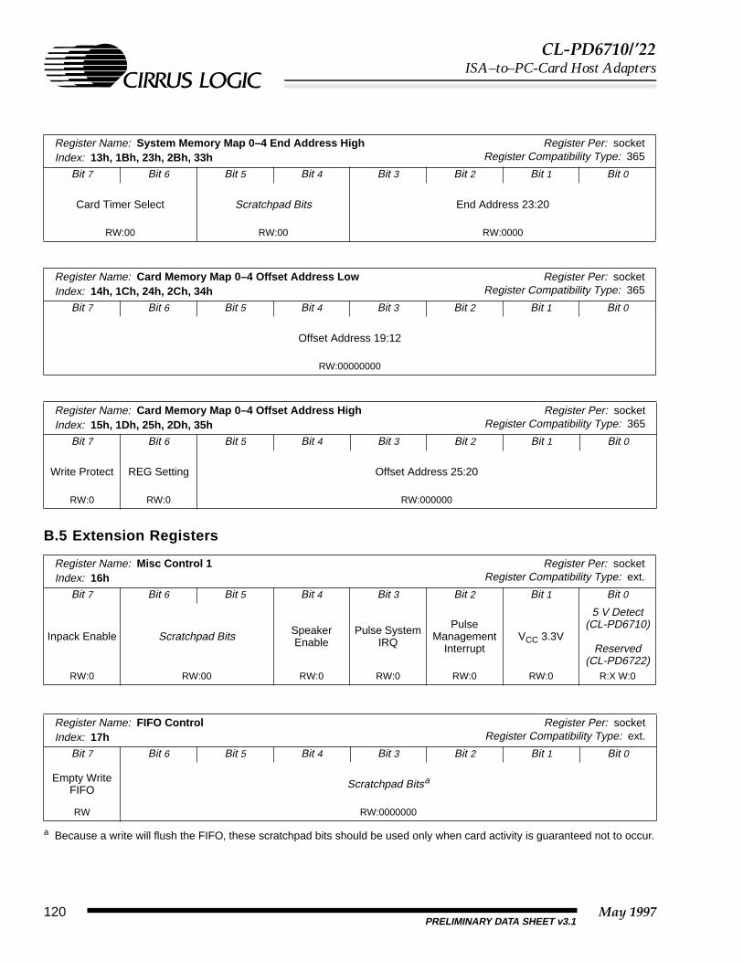
CL-PD6710/’22ISA–to–PC-Card Host Adapters
B.5 Extension Registers
a Because a write will flush the FIFO, these scratchpad bits should be used only when card activity is guaranteed not to occur.
Register Name: System Memory Map 0–4 End Address HighIndex: 13h, 1Bh, 23h, 2Bh, 33h
Register Per: socketRegister Compatibility Type: 365
Bit 7 Bit 6 Bit 5 Bit 4 Bit 3 Bit 2 Bit 1 Bit 0
Card Timer Select Scratchpad Bits End Address 23:20
RW:00 RW:00 RW:0000
Register Name: Card Memory Map 0–4 Offset Address LowIndex: 14h, 1Ch, 24h, 2Ch, 34h
Register Per: socketRegister Compatibility Type: 365
Bit 7 Bit 6 Bit 5 Bit 4 Bit 3 Bit 2 Bit 1 Bit 0
Offset Address 19:12
RW:00000000
Register Name: Card Memory Map 0–4 Offset Address HighIndex: 15h, 1Dh, 25h, 2Dh, 35h
Register Per: socketRegister Compatibility Type: 365
Bit 7 Bit 6 Bit 5 Bit 4 Bit 3 Bit 2 Bit 1 Bit 0
Write Protect REG Setting Offset Address 25:20
RW:0 RW:0 RW:000000
Register Name: Misc Control 1Index: 16h
Register Per: socketRegister Compatibility Type: ext.
Bit 7 Bit 6 Bit 5 Bit 4 Bit 3 Bit 2 Bit 1 Bit 0
Inpack Enable Scratchpad Bits Speaker Enable
Pulse System IRQ
Pulse Management
InterruptVCC 3.3V
5 V Detect (CL-PD6710)
Reserved (CL-PD6722)
RW:0 RW:00 RW:0 RW:0 RW:0 RW:0 R:X W:0
Register Name: FIFO ControlIndex: 17h
Register Per: socketRegister Compatibility Type: ext.
Bit 7 Bit 6 Bit 5 Bit 4 Bit 3 Bit 2 Bit 1 Bit 0
Empty Write FIFO Scratchpad Bitsa
RW RW:0000000
PRELIMINARY DATA SHEET v3.1May 1997120
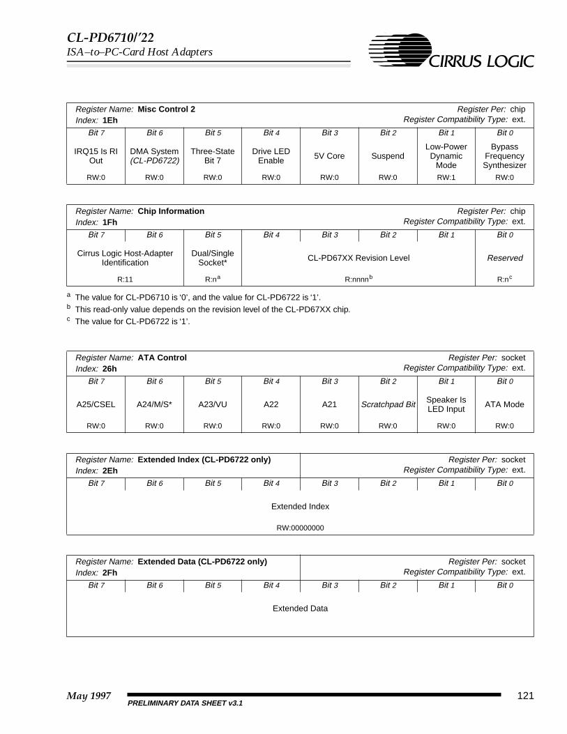
CL-PD6710/’22ISA–to–PC-Card Host Adapters
a The value for CL-PD6710 is ‘0’, and the value for CL-PD6722 is ‘1’.b This read-only value depends on the revision level of the CL-PD67XX chip.c The value for CL-PD6722 is ‘1’.
Register Name: Misc Control 2Index: 1Eh
Register Per: chipRegister Compatibility Type: ext.
Bit 7 Bit 6 Bit 5 Bit 4 Bit 3 Bit 2 Bit 1 Bit 0
IRQ15 Is RI Out
DMA System (CL-PD6722)
Three-State Bit 7
Drive LED Enable 5V Core Suspend
Low-Power Dynamic
Mode
Bypass Frequency Synthesizer
RW:0 RW:0 RW:0 RW:0 RW:0 RW:0 RW:1 RW:0
Register Name: Chip InformationIndex: 1Fh
Register Per: chipRegister Compatibility Type: ext.
Bit 7 Bit 6 Bit 5 Bit 4 Bit 3 Bit 2 Bit 1 Bit 0
Cirrus Logic Host-Adapter Identification
Dual/Single Socket* CL-PD67XX Revision Level Reserved
R:11 R:na R:nnnnb R:nc
Register Name: ATA ControlIndex: 26h
Register Per: socketRegister Compatibility Type: ext.
Bit 7 Bit 6 Bit 5 Bit 4 Bit 3 Bit 2 Bit 1 Bit 0
A25/CSEL A24/M/S* A23/VU A22 A21 Scratchpad Bit Speaker Is LED Input ATA Mode
RW:0 RW:0 RW:0 RW:0 RW:0 RW:0 RW:0 RW:0
Register Name: Extended Index (CL-PD6722 only)Index: 2Eh
Register Per: socketRegister Compatibility Type: ext.
Bit 7 Bit 6 Bit 5 Bit 4 Bit 3 Bit 2 Bit 1 Bit 0
Extended Index
RW:00000000
Register Name: Extended Data (CL-PD6722 only)Index: 2Fh
Register Per: socketRegister Compatibility Type: ext.
Bit 7 Bit 6 Bit 5 Bit 4 Bit 3 Bit 2 Bit 1 Bit 0
Extended Data
May 1997 121PRELIMINARY DATA SHEET v3.1

CL-PD6710/’22ISA–to–PC-Card Host Adapters
Register Name: Data Mask 0 (CL-PD6722 only)Index: 2Fh
Extended Index: 01h
Register Per: socketRegister Compatibility Type: ext.
Bit 7 Bit 6 Bit 5 Bit 4 Bit 3 Bit 2 Bit 1 Bit 0
Data Mask Select 0
RW:00000000
Register Name: Data Mask 1(CL-PD6722 only)Index: 2Fh
Extended Index: 02h
Register Per: socketRegister Compatibility Type: ext.
Bit 7 Bit 6 Bit 5 Bit 4 Bit 3 Bit 2 Bit 1 Bit 0
Data Mask Select 1
RW:00000000
Register Name: Extension Control 1(CL-PD6722 only)Index: 2Fh
Extended Index: 03h
Register Per: socketRegister Compatibility Type: ext.
Bit 7 Bit 6 Bit 5 Bit 4 Bit 3 Bit 2 Bit 1 Bit 0
DMA Enable Pull-up Control Reserved LED Activity
EnableAuto Power
Clear DisableVCC Power
Lock
RW:00 RW:0 RW:00 RW:0 RW:0 RW:0
Register Name: Maximum DMAAcknowledge Delay (CL-PD6722 only)Index: 2Fh Extended Index: 04h
Register Per: socketRegister Compatibility Type: ext.
Bit 7 Bit 6 Bit 5 Bit 4 Bit 3 Bit 2 Bit 1 Bit 0
Maximum DMA Acknowledge Delay
RW:00000000
Register Name: External Data (CL-PD6722 only)Index: 2Fh
Extended Index: 0Ah
Register Per: socketRegister Compatibility Type: ext.
Bit 7 Bit 6 Bit 5 Bit 4 Bit 3 Bit 2 Bit 1 Bit 0
External Data 7
External Data 6
External Data 5
External Data 4
External Data 3
External Data 2
External Data 1
External Data 0
RW:0 RW:0 RW:0 RW:0 RW:0 RW:0 RW:0 RW:0
PRELIMINARY DATA SHEET v3.1May 1997122
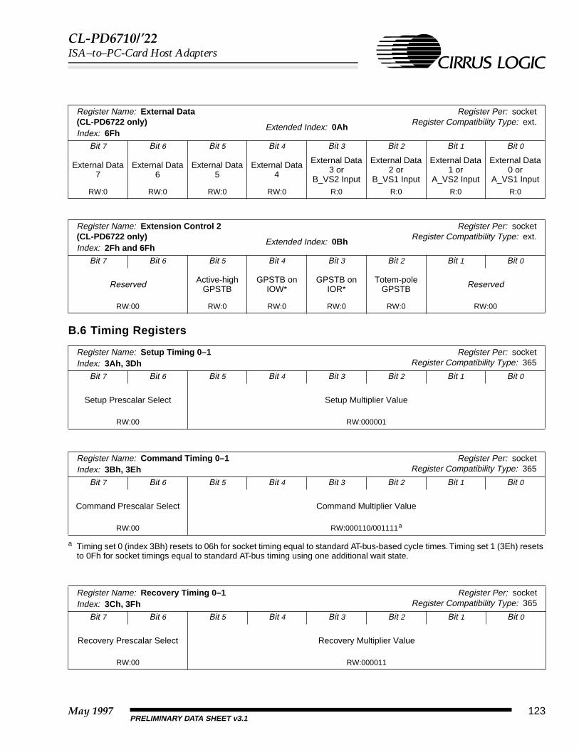
CL-PD6710/’22ISA–to–PC-Card Host Adapters
B.6 Timing Registers
a Timing set 0 (index 3Bh) resets to 06h for socket timing equal to standard AT-bus-based cycle times. Timing set 1 (3Eh) resets to 0Fh for socket timings equal to standard AT-bus timing using one additional wait state.
Register Name: External Data (CL-PD6722 only)Index: 6Fh
Extended Index: 0Ah
Register Per: socketRegister Compatibility Type: ext.
Bit 7 Bit 6 Bit 5 Bit 4 Bit 3 Bit 2 Bit 1 Bit 0
External Data 7
External Data 6
External Data 5
External Data 4
External Data 3 or
B_VS2 Input
External Data 2 or
B_VS1 Input
External Data 1 or
A_VS2 Input
External Data 0 or
A_VS1 InputRW:0 RW:0 RW:0 RW:0 R:0 R:0 R:0 R:0
Register Name: Extension Control 2(CL-PD6722 only)Index: 2Fh and 6Fh
Extended Index: 0Bh
Register Per: socketRegister Compatibility Type: ext.
Bit 7 Bit 6 Bit 5 Bit 4 Bit 3 Bit 2 Bit 1 Bit 0
Reserved Active-high GPSTB
GPSTB on IOW*
GPSTB on IOR*
Totem-pole GPSTB Reserved
RW:00 RW:0 RW:0 RW:0 RW:0 RW:00
Register Name: Setup Timing 0–1Index: 3Ah, 3Dh
Register Per: socketRegister Compatibility Type: 365
Bit 7 Bit 6 Bit 5 Bit 4 Bit 3 Bit 2 Bit 1 Bit 0
Setup Prescalar Select Setup Multiplier Value
RW:00 RW:000001
Register Name: Command Timing 0–1Index: 3Bh, 3Eh
Register Per: socketRegister Compatibility Type: 365
Bit 7 Bit 6 Bit 5 Bit 4 Bit 3 Bit 2 Bit 1 Bit 0
Command Prescalar Select Command Multiplier Value
RW:00 RW:000110/001111a
Register Name: Recovery Timing 0–1Index: 3Ch, 3Fh
Register Per: socketRegister Compatibility Type: 365
Bit 7 Bit 6 Bit 5 Bit 4 Bit 3 Bit 2 Bit 1 Bit 0
Recovery Prescalar Select Recovery Multiplier Value
RW:00 RW:000011
May 1997 123PRELIMINARY DATA SHEET v3.1

CL-PD6710/’22ISA–to–PC-Card Host Adapters
INDEX
Numerics+5V 205V Core bit 61
AA[25:0] 16A_ pin name 16
See also the pin nameA21 bit 64A22 bit 64A23/VU bit 64A24/M/S* bit 64A25/CSEL bit 64AC specifications 91–109Active-high GPSTB bit 71AEN 13ALE 12ATA Control register 64ATA mode
description 75overview 29pin cross reference 75
ATA Mode bit 64Auto Power Clear Disable bit 66Auto-Power bit 41Auto-Size I/O Window 0 bit 49Auto-Size I/O Window 1 bit 49
BB_ pin name 16
See also the pin nameBattery Dead Or Status Change bit 44Battery Dead Or Status Change Enable bit 45Battery Voltage Detect bits 38Battery Warning Change bit 44Battery Warning Enable bit 45BBS (bulletin board system) 114bus sizing 29BVD1/-STSCHG/-RI 19BVD2/-SPKR/-LED 18Bypass Frequency Synthesizer bit 61
CC_SEL 15Card Detect bits 38Card Detect Change bit 44Card Detect Enable bit 45Card Enable bit 41Card I/O Map 0–1 Address Offset High registers 52
Card I/O Map 0–1 Address Offset Low registers 52Card IRQ Select bits 42Card Is I/O bit 42Card Memory Map 0–4 Offset Address High
registers 56Card Memory Map 0–4 Offset Address Low
registers 56Card Power On bit 39Card Reset* bit 43Card Status Change register 44Card Timer Select bits 55-CD[2:1] 18-CE[2:1] 18Chip Identification bits. See Cirrus Logic Host-Adapter
Identification bitsChip Information register 63Chip Revision register 37Cirrus Logic Host-Adapter Identification bits 63CLK 15CL-PD67XX Revision Level bits 63Command Multiplier Value bits 73Command Prescalar Select bits 73Command Timing 0–1 registers 73conventions
bit naming 32general 7numbers and units 7pin naming 11register headings 32
CORE_VDD 20
DD[15:0] 16Data Mask 0–1 register 66Data Mask Select 0–1 bits 66Data register 36DC specifications 87–90Device Index bit 33DMA Control register. See Extension Control 1 registerDMA Enable bits 67DMA mode
configuring 84–86description 83overview 30
DMA Read Cycle timing 105DMA Request timing 109DMA System bit 62DMA Write Cycle timing 107Drive LED Enable bit 61Dual/Single Socket* bit 63
PRELIMINARY DATA SHEET v3.1May 1997124
INDEX

CL-PD6710/’22ISA–to–PC-Card Host Adapters
EEmpty Write FIFO bit 60Enable Manage Int bit 42End Address
15:8 bits 5119:12 bits 5523:20 bits 557:0 bits 51
Extended Data register 65Extended Index register 65Extended Register Index bits 65Extension Control 1 register 66Extension Control 2 register 71External Data bits 69–70External Data register 69
FFIFO Control register 60form factor 1–2, 110, 112functional blocks 25
Ggeneral-purpose strobe
control 77description 77–80example implementations 79overview 26suspend mode 80
General-Purpose Strobe timing 96GND 20GPSTB 19GPSTB on IOR* bit 71GPSTB on IOW* bit 71
Hhost access to registers 30
II/O Map 0 Enable bit 48I/O Map 0–1 Start Address High registers 50I/O Map 1 Enable bit 48I/O Window 0 Size bit 49I/O Window 1 Size bit 49I/O Window Control register 49IDE 75Index register 33-INPACK 17Inpack Enable bit 59Input Clock specification 97Interface ID bits 37
Interface Status register 38Interrupt and General Control register 42interrupts 25-INTR 14IOCHRDY 13IOCS16* 13-IOIS16 17IOR* 12-IORD 17IOW* 12-IOWR 17-IREQ 17IRQ Level bits. See Card IRQ Select bitsIRQ[14, 11, 7, 5:3] 13IRQ10 13IRQ10 as DRQ, description 26IRQ12 as LED_OUT*, description 26IRQ12/LED_OUT* 14IRQ15 as RI_OUT*, description 26IRQ15 Is RI Out bit 62IRQ15/RI_OUT* 14IRQ9 13IRQ9 as DACK*, description 26ISA bus interface pins 12–15ISA bus timing 92ISA_VCC 15
LLA[23:17] 12-LED 18LED Activity Enable bit 66LED_OUT* 14Low-Power Dynamic mode 27Low-Power Dynamic Mode bit 61
MManagement Interrupt Configuration register 45Management IRQ Select bits 46Mapping Enable register 47MEMCS16 Full Decode bit 47MEMCS16* 13Memory Map
0 Enable bit 471 Enable bit 472 Enable bit 473 Enable bit 474 Enable bit 47
MEMR* 12MEMW* 12Misc Control 1 register 58Misc Control 2 register 61
May 1997 125PRELIMINARY DATA SHEET v3.1 INDEX

CL-PD6710/’22ISA–to–PC-Card Host Adapters
NNormal Byte Read/Write timing 103
OOdd Byte timing 104-OE 16Offset Address
15:8 bits 5219:12 bits 5625:20 bits 577:1 bits 52
ordering information 113
Ppackage
144-pin VQFP 110208-pin PQFP 111208-pin VQFP 112
PC Cardbasics 22bus timing calculations 98Read/Write timing 102socket timing 99timing 29
PCMCIA 22pin descriptions 8, 20pin diagram
144-pin VQFP 9208-pin PQFP or VQFP 10
pin usage summary 21power consumption 28Power Control register 40power management 27power-on
configuration 21setup 31
Pull-up Control bit 67Pulse Management Interrupt bit 58Pulse Mode Interrupt timing 95Pulse System IRQ bit 59PWRGOOD 12
RRDY/-IREQ 17Ready Change bit 44Ready Enable bit 45Ready/Busy* bit 39Recovery Multiplier Value bits 74Recovery Prescalar Select bits 74Recovery Timing 0–1 registers 74
REFRESH* 12-REG 16REG Setting bit 57Register Index bits 33register summary tables 116–123RESET 18Reset timing 94Revision bits 37-RI 19RI_OUT* 14Ring Indicate Enable bit 43
SSA[16:0] 12SBHE* 12SD[15:0] 12Setup Multiplier Value bits 72Setup Prescalar Select bit 72Setup Timing 0–1 registers 72SLOT_VCC. See SOCKET_VCCsocket
accessing specific registers 33register per 32
Socket Index bit 33socket interface pins 16–19socket power features 28SOCKET_VCC 19Speaker Enable bit 59Speaker Is LED Input bit 64-SPKR 18SPKR_OUT*/C_SEL 15Start Address
15:8 bits 5019:12 bits 5323:20 bits 547:0 bits 50
-STSCHG 19Super-Suspend mode, description 27Suspend bit 61Suspend mode, description 27System I/O Map 0–1
End Address High registers 51End Address Low registers 51Start Address Low registers 50
System Interrupt timing 95System Memory Map 0–4
End Address High registers 55End Address Low registers 54Start Address High registers 54Start Address Low registers 53
PRELIMINARY DATA SHEET v3.1May 1997126
INDEX

CL-PD6710/’22ISA–to–PC-Card Host Adapters
TThree-State Bit 7 bit 62timing
DMA Read Cycle 105DMA request 109DMA Write Cycle 107General-Purpose Strobe 96ISA bus 92Normal Byte Read/Write 103Odd Byte 104PC Card bus 98PC Card Read/Write 102PC Card socket 99Pulse Mode Interrupt 95Reset 94System Interrupt 95Word I/O Read/Write 100
Timing Register Select 0 bit 49Timing Register Select 1 bit 50Totem-pole GPSTB bit 71
VVCC 3.3V bit 58VCC Power bit 41
VCC Power Lock bit 66-VCC_3 20-VCC_5 20VDD. See CORE_VDDvoltage sense 81–82
overview 27VPP Valid bit 39VPP_PGM 20-VPP_VALID 15VPP_VCC 20VPP1 Power bits 41
W-WAIT 18-WE 17Window Data Size bit 54windowing 22Word I/O Read/Write timing 100WP/-IOIS16 17write FIFO 29Write Protect bit 38, 57
ZZWS* 14
May 1997 127PRELIMINARY DATA SHEET v3.1 INDEX

CL-PD6710/’22Preliminary Data Sheet v3.1
Direct Sales Offices
Domestic
N. CALIFORNIAFremontTEL: 510/623-8300FAX: 510/252-6020
S. CALIFORNIAWestlake VillageTEL: 805/371-5860FAX: 805/371-5861
NORTHWESTERN AREAPortland, ORTEL: 503/620-5547FAX: 503/620-5665
SOUTH CENTRALAREAAustin, TXTEL: 512/255-0080FAX: 512/255-0733
Cirrus Logic Inc.3100 West Warren Ave., FremTEL: 510/623-8300 FAX: 5
The CompanyHeadquartered in Fremon
desktop and portable compulevel expertise in analog and
Cirrus Logic has developmultimedia, graphics, comm
The Cirrus Logic formulacomplete solutions — chips,marketplace.
Cirrus Logic’s manufactucustomers.
Talk to our systems and company.
Preliminary product information descrmade best efforts to ensure that the innotice. No responsibility is assumed bdocument is the property of Cirrus Loreproduced, stored in a retrieval systebasis for manufacture or sale of any itFastPath, FasText, FeatureChips, FiSofTarget, Systems in Silicon, Textureof Cirrus Logic Inc., which may be regCirrus Logic International, Ltd. are tra
Irving, TXTEL: 972/252-6698FAX: 972/252-5681
Houston, TXTEL: 281/257-2525FAX: 281/257-2555
NORTHEASTERN AREAAndover, MATEL: 508/474-9300FAX: 508/474-9149
SOUTHEASTERN AREARaleigh, NCTEL: 919/859-5210FAX: 919/859-5334
Boca Raton, FLTEL: 407/241-2364FAX: 407/241-7990
Pont, CA 94538 W10/252-6020
t, California, Cirrus Logic is ating, telecommunications, an digital design to innovate hi
ed a broad portfolio of produunications, system logic, mas
combines innovative architec software, evaluation boards, a
ring strategy ensures maximu
applications specialists; see ho
ibes products that are in production, buformation contained in this document isy Cirrus Logic Inc. for the use of this infgic Inc. and implies no license under pam, or transmitted, in any form or by an
ems without the prior written consent oflterJet, Get into it, Good Data, LagunaJet, TVTap, UXART, Video Port Manageistered in some jurisdictions. Other tra
de names of Cirrus Logic Inc.
International
CHINABeijingTEL: 86/10-642-807-83-5FAX: 86/19-672-807-86
FRANCEParisTEL: 33/1-48-12-2812FAX: 33/1-48-12-2810
GERMANYHerrschingTEL: 49/81-52-92460FAX: 49/81-52-924699
HONG KONGTsimshatsuiTEL: 852/2376-0801FAX: 852/2375-1202
ITALYMilanTEL: 39/2-3360-5458FAX: 39/2-3360-5426
ublications Ordering: 800/359orld Wide Web: http://w
leading manufacturer of advad consumer electronics. The Cghly integrated, software-rich
cts and technologies for applis storage, and data acquisitio
tures in silicon with system dnd manufacturing kits — on-
m product quality, availabili
w you can benefit from a new
Copyright 1997 Cirrus Lo
t for which full characterization data is n accurate and reliable. However, the infoormation, nor for infringements of patentents, copyrights, or trade secrets. No py means, electronic, mechanical, photo Cirrus Logic Inc. Cirrus, Cirrus Logic, A, Laguna3D, MediaDAC, MotionVideo
r, VisualMedia, VPM, V-Port, Voyager, Wdemarks in this document belong to the
JAPANTokyoTEL: 81/3-3340-9111FAX: 81/3-3340-9120
KOREASeoulTEL: 82/2-565-8561FAX: 82/2-565-8565
SINGAPORETEL: 65/743-4111FAX: 65/742-4111
TAIWANTaipeiTEL: 886/2-718-4533FAX: 886/2-718-4526
UNITED KINGDOMLondon, EnglandTEL: 44/1727-872424FAX: 44/1727-875919
-6414 (USA) or 510/249-4200ww.cirrus.com
346710-005
nced integrated circuits for ompany applies its system- solutions.
cations spanning n.
esign expertise. We deliver time, to help you win in the
ty, and value for our
kind of semiconductor
gic Inc. All rights reserved.
ot yet available. Cirrus Logic Inc. hasrmation is subject to change without
ts or other rights of third parties. Thisart of this publication may be copied,graphic, or otherwise, or used as theccuPak, Clear3D, DirectVPM, DIVA,
, RSA, SimulSCAN, S/LA, SMASH,avePort, and WebSet are trademarksir respective companies. CRUS and