Embed Size (px)
Citation preview
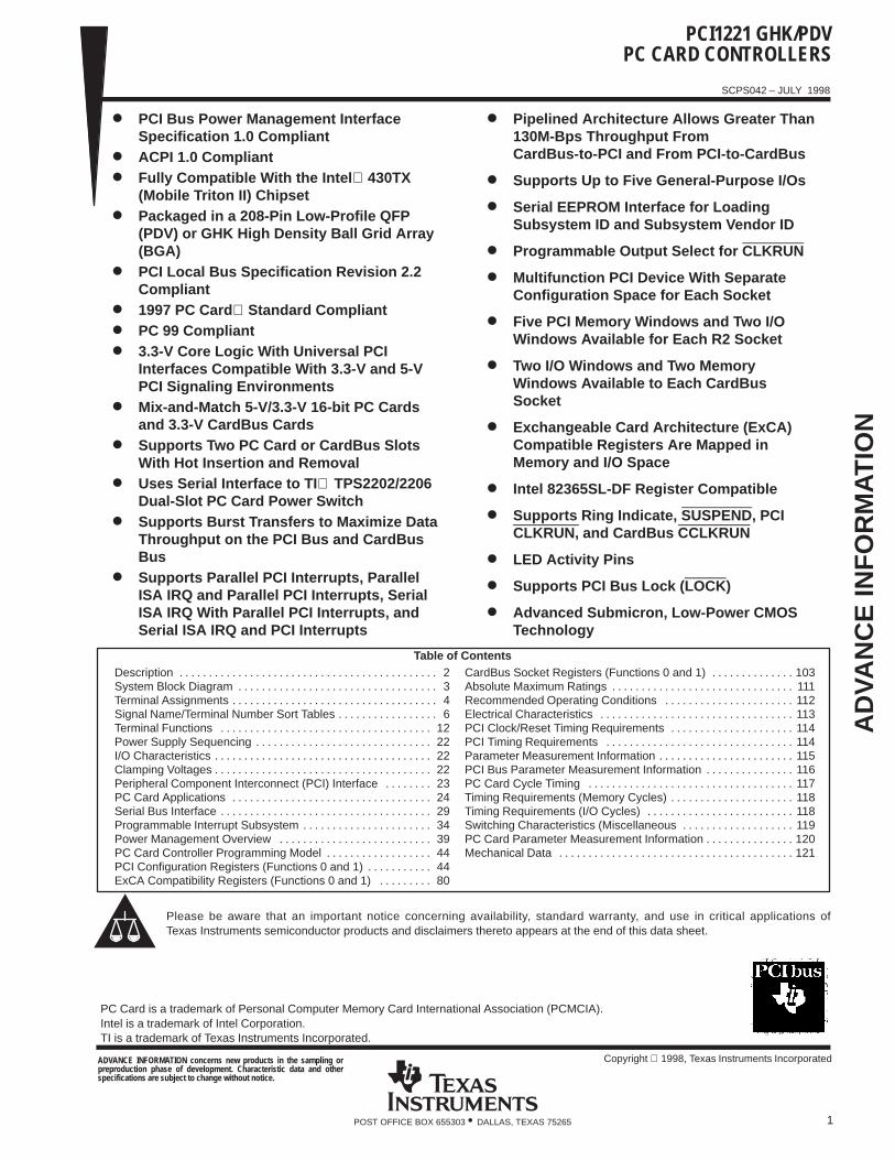
PCI1221 GHK/PDVPC CARD CONTROLLERS
SCPS042 – JULY 1998
1POST OFFICE BOX 655303 • DALLAS, TEXAS 75265
PCI Bus Power Management InterfaceSpecification 1.0 Compliant
ACPI 1.0 Compliant Fully Compatible With the Intel 430TX
(Mobile Triton II) Chipset Packaged in a 208-Pin Low-Profile QFP
(PDV) or GHK High Density Ball Grid Array(BGA)
PCI Local Bus Specification Revision 2.2Compliant
1997 PC Card Standard Compliant PC 99 Compliant 3.3-V Core Logic With Universal PCI
Interfaces Compatible With 3.3-V and 5-VPCI Signaling Environments
Mix-and-Match 5-V/3.3-V 16-bit PC Cardsand 3.3-V CardBus Cards
Supports Two PC Card or CardBus SlotsWith Hot Insertion and Removal
Uses Serial Interface to TI TPS2202/2206Dual-Slot PC Card Power Switch
Supports Burst Transfers to Maximize DataThroughput on the PCI Bus and CardBusBus
Supports Parallel PCI Interrupts, ParallelISA IRQ and Parallel PCI Interrupts, SerialISA IRQ With Parallel PCI Interrupts, andSerial ISA IRQ and PCI Interrupts
Pipelined Architecture Allows Greater Than130M-Bps Throughput FromCardBus-to-PCI and From PCI-to-CardBus
Supports Up to Five General-Purpose I/Os
Serial EEPROM Interface for LoadingSubsystem ID and Subsystem Vendor ID
Programmable Output Select for CLKRUN
Multifunction PCI Device With SeparateConfiguration Space for Each Socket
Five PCI Memory Windows and Two I/OWindows Available for Each R2 Socket
Two I/O Windows and Two MemoryWindows Available to Each CardBusSocket
Exchangeable Card Architecture (ExCA)Compatible Registers Are Mapped inMemory and I/O Space
Intel 82365SL-DF Register Compatible
Supports Ring Indicate, SUSPEND , PCICLKRUN, and CardBus CCLKRUN
LED Activity Pins
Supports PCI Bus Lock (LOCK )
Advanced Submicron, Low-Power CMOSTechnology
Description 2. . . . . . . . . . . . . . . . . . . . . . . . . . . . . . . . . . . . . . . . . . . . System Block Diagram 3. . . . . . . . . . . . . . . . . . . . . . . . . . . . . . . . . . Terminal Assignments 4. . . . . . . . . . . . . . . . . . . . . . . . . . . . . . . . . . . Signal Name/Terminal Number Sort Tables 6. . . . . . . . . . . . . . . . . Terminal Functions 12. . . . . . . . . . . . . . . . . . . . . . . . . . . . . . . . . . . . Power Supply Sequencing 22. . . . . . . . . . . . . . . . . . . . . . . . . . . . . . I/O Characteristics 22. . . . . . . . . . . . . . . . . . . . . . . . . . . . . . . . . . . . . Clamping Voltages 22. . . . . . . . . . . . . . . . . . . . . . . . . . . . . . . . . . . . . Peripheral Component Interconnect (PCI) Interface 23. . . . . . . . PC Card Applications 24. . . . . . . . . . . . . . . . . . . . . . . . . . . . . . . . . . Serial Bus Interface 29. . . . . . . . . . . . . . . . . . . . . . . . . . . . . . . . . . . . Programmable Interrupt Subsystem 34. . . . . . . . . . . . . . . . . . . . . . Power Management Overview 39. . . . . . . . . . . . . . . . . . . . . . . . . . PC Card Controller Programming Model 44. . . . . . . . . . . . . . . . . . PCI Configuration Registers (Functions 0 and 1) 44. . . . . . . . . . . ExCA Compatibility Registers (Functions 0 and 1) 80. . . . . . . . .
CardBus Socket Registers (Functions 0 and 1) 103. . . . . . . . . . . . . . Absolute Maximum Ratings 111. . . . . . . . . . . . . . . . . . . . . . . . . . . . . . . Recommended Operating Conditions 112. . . . . . . . . . . . . . . . . . . . . . Electrical Characteristics 113. . . . . . . . . . . . . . . . . . . . . . . . . . . . . . . . . PCI Clock/Reset Timing Requirements 114. . . . . . . . . . . . . . . . . . . . . PCI Timing Requirements 114. . . . . . . . . . . . . . . . . . . . . . . . . . . . . . . . Parameter Measurement Information 115. . . . . . . . . . . . . . . . . . . . . . . PCI Bus Parameter Measurement Information 116. . . . . . . . . . . . . . . PC Card Cycle Timing 117. . . . . . . . . . . . . . . . . . . . . . . . . . . . . . . . . . . Timing Requirements (Memory Cycles) 118. . . . . . . . . . . . . . . . . . . . . Timing Requirements (I/O Cycles) 118. . . . . . . . . . . . . . . . . . . . . . . . . Switching Characteristics (Miscellaneous 119. . . . . . . . . . . . . . . . . . . PC Card Parameter Measurement Information 120. . . . . . . . . . . . . . . Mechanical Data 121. . . . . . . . . . . . . . . . . . . . . . . . . . . . . . . . . . . . . . . .
Table of Contents
Please be aware that an important notice concerning availability, standard warranty, and use in critical applications ofTexas Instruments semiconductor products and disclaimers thereto appears at the end of this data sheet.
Copyright 1998, Texas Instruments Incorporated
PC Card is a trademark of Personal Computer Memory Card International Association (PCMCIA).Intel is a trademark of Intel Corporation.TI is a trademark of Texas Instruments Incorporated.
ADVANCE INFORMATION concerns new products in the sampling orpreproduction phase of development. Characteristic data and otherspecifications are subject to change without notice.
AD
VA
NC
E IN
FO
RM
ATIO
N

PCI1221 GHK/PDVPC CARD CONTROLLERS
SCPS042 – JULY 1998
2 POST OFFICE BOX 655303 • DALLAS, TEXAS 75265
description
The TI PCI1221 is a high-performance PCI-to-PC Card controller that supports two independent card socketscompliant with the 1997 PC Card Standard. The PCI1221 provides a rich feature set that makes it the bestchoice for bridging between PCI and PC Cards in both notebook and desktop computers. The 1997 PC CardStandard retains the 16-bit PC Card specification defined in PCMCIA Release 2.2 and defines the new 32-bitPC Card, CardBus, capable of full 32-bit data transfers at 33 MHz. The PCI1221 supports any combination of16-bit and CardBus PC Cards in the two sockets, powered at 5 V or 3.3 V, as required.
The PCI1221 is compliant with the PCI Local Bus Specification 2.2, and its PCI interface can act as either a PCImaster device or a PCI slave device. The PCI bus mastering is initiated during CardBus PC Card bridgingtransactions. The PCI1221 is also compliant with the latest PCI Bus Power Management Interface Specification.
All card signals are internally buffered to allow hot insertion and removal without external buffering. The PCI1221is register compatible with the Intel 82365SL-DF ExCA controller. The PCI1221 internal data path logic allowsthe host to access 8-, 16-, and 32-bit cards using full 32-bit PCI cycles for maximum performance. Independentbuffering and a pipeline architecture provide an unsurpassed performance level with sustained bursting. ThePCI1221 can also be programmed to accept fast posted writes to improve system-bus utilization.
Multiple system-interrupt signaling options are provided, including: parallel PCI, parallel ISA, serialized ISA, andserialized PCI. Furthermore, general-purpose inputs and outputs are provided for the board designer toimplement sideband functions. Many other features designed into the PCI1221, such as socket activitylight-emitting diode (LED) outputs, are discussed in detail throughout the design specification.
An advanced complementary metal-oxide semiconductor (CMOS) process is used to achieve lowsystem-power consumption while operating at PCI clock rates up to 33 MHz. Several low-power modes enablethe host power management system to further reduce power consumption.
Unused PCI1221 inputs must be pulled up using a 43k-resistor.
PCI1221 GHK/PDVPC CARD CONTROLLERS
SCPS042 – JULY 1998
3POST OFFICE BOX 655303 • DALLAS, TEXAS 75265
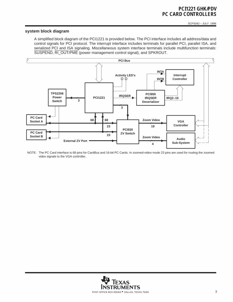
system block diagram
A simplified block diagram of the PCI1221 is provided below. The PCI interface includes all address/data andcontrol signals for PCI protocol. The interrupt interface includes terminals for parallel PCI, parallel ISA, andserialized PCI and ISA signaling. Miscellaneous system interface terminals include multifunction terminals:SUSPEND, RI_OUT/PME (power management control signal), and SPKROUT.
PCI Bus
PCI1221
Activity LED’s
PCI950IRQSER
Deserializer
IRQSER
3
InterruptController
INTA
INTB
IRQ2–15
PCI930ZV Switch23
23
PC CardSocket A
TPS2206PowerSwitch 3
PC CardSocket B
External ZV Port
VGAController
AudioSub-System
Zoom Video
19
4
Zoom Video
NOTE: The PC Card interface is 68 pins for CardBus and 16-bit PC Cards. In zoomed-video mode 23 pins are used for routing the zoomedvideo signals to the VGA controller.
68 68
PCI1221 GHK/PDVPC CARD CONTROLLERS
SCPS042 – JULY 1998
4 POST OFFICE BOX 655303 • DALLAS, TEXAS 75265
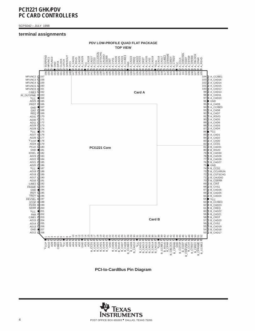
terminal assignments
B_CCLKRUN
A_C
AD
25
A_CAD13
A_CAD0
B_C
AD
9
B_C
AD
1
B_C
CD
1
AD
4
AD17
CC
PA
D10
AD
9A
D8
AD
7
AD
6A
D5
AD
3
GN
DA
D1
AD
0
B_C
AD
0B
_CA
D2
B_C
AD
4B
_CA
D3
GN
DB
_CA
D6
B_C
AD
5B
_RS
VD
B_C
AD
7
B_C
C/B
E0
B_C
AD
10
B_C
AD
11
B_C
AD
14
B_C
AD
12B
_CA
D15
B_C
AD
16
B_C
PA
R
B_C
PE
RR
GN
DB
_CS
TO
PB
_CG
NT
B_C
IRD
Y
B_C
DE
VS
EL
B_C
CLK
B_C
TR
DY
B_C
FR
AM
EB
_CC
/BE
2
AD
2
B_C
AD
8
B_C
AD
13
B_C
C/B
E1
B_R
SV
D
B_C
BLO
CK
MFUNC2
C/BE3RI_OUT/PME
AD25
GND
REQ
PRST
AD11
AD31AD30
AD29AD28
AD27
AD24PCLKGND
IDSEL
AD22
AD20
AD26
AD23
AD16
FRAMEGNDIRDY
DEVSEL
PERRSERR
PAR
AD15AD14AD13GND
AD12
A_CC/BE1A_CAD16A_CAD14
A_CAD12
A_CAD11A_CAD10GND
A_CAD7
A_CAD9A_CC/BE0A_CAD8
A_RSVDA_CAD5A_CAD6
A_CAD4
A_CAD1A_CAD2
A_CCD1B_CAD31B_RSVDB_CAD30B_CAD29B_CAD28B_CAD27GNDB_CCD2
B_CSTSCHGB_CAUDIO
B_CVS1B_CAD26B_CAD25
B_CSERR
B_CC/BE3
B_CAD24V
B_CAD23B_CREQB_CAD22B_CAD21B_CRSTB_CAD20B_CVS2B_CAD19B_CAD18B_CAD17
158157
160159
162161
164163
166165
168167
170169
172171
174173
176175
178177
180179
182181
184183
186185
188187
190189
192191
194193
196195
198197
200199
202201
204203
206205
208207
103104
101102
99100
9798
9596
9394
9192
8990
8788
8586
8384
8182
7980
7778
7576
7374
7172
6970
6768
6566
6364
6162
5960
5758
5556
5354
A_CAD3
B_CINT
A_CAD15
21 43 65 87 109 1211 1413 1615 1817 2019 2221 2423 2625 2827 3029 3231 3433 3635 3837 4039 4241 4443 4645 4847 5049 525110
610
5
108
107
110
109
112
111
114
113
116
115
118
117
120
119
122
121
124
123
126
125
128
127
130
129
132
131
134
133
136
135
138
137
140
139
142
141
144
143
146
145
148
147
150
149
152
151
154
153
156
155
SU
SP
EN
D
GN
DM
FU
NC
0
DA
TA
SP
KR
OU
TLA
TC
HC
LOC
K
A_C
AD
31V
CC
I
A_C
AD
30A
_RS
VD
A_C
AD
28
A_C
AD
29
A_C
CD
2A
_CA
D27
A_C
CLK
RU
N
A_C
AU
DIO
A_C
ST
SC
HG
A_C
INT
A_C
SE
RR
A_C
AD
26A
_CV
S1
A_C
C/B
E3
A_C
AD
24
A_C
AD
23G
ND
A_C
AD
21A
_CA
D22
A_C
RE
Q
A_C
AD
20A
_CR
ST
A_C
AD
19A
_CV
S2
A_C
AD
18
A_C
FR
AM
EA
_CC
/BE
2
A_C
TR
DY
A_C
IRD
Y
A_C
CLK
V A_C
DE
VS
EL
A_C
AD
17
A_C
ST
OP
A_C
GN
T
A_C
BLO
CK
A_C
PE
RR
A_R
SV
DA
_CP
AR
GNT
AD21
AD19AD18
TRDY
STOP
PCI-to-CardBus Pin Diagram
V C/B
E0
CC
V CC
V CC
BV
CC
VCC
CC
VC
CA
VC
C
MF
UN
C1
MFUNC3MFUNC4MFUNC5MFUNC6
VCC
VCC
VCC
C/BE2
VCC
C/BE1
CCPV
Card A
Card B
PCI1221 Core
PDV LOW-PROFILE QUAD FLAT PACKAGETOP VIEW
PCI1221 GHK/PDVPC CARD CONTROLLERS
SCPS042 – JULY 1998
5POST OFFICE BOX 655303 • DALLAS, TEXAS 75265
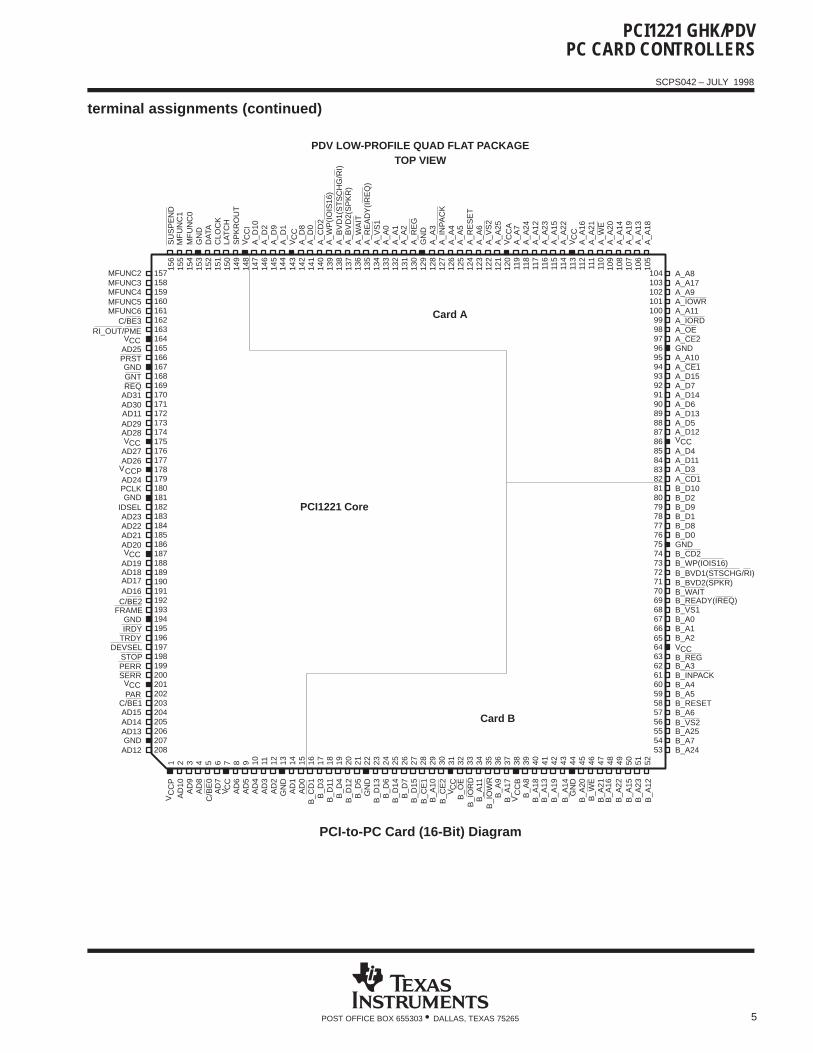
terminal assignments (continued)
C/BE1
B_C
D1
A_A
1
A_D3
B_A
10
B_D
4
AD
4
AD18
CC
PA
D10
AD
9A
D8
AD
7
AD
6A
D5
AD
3
GN
DA
D1
AD
0
B_D
3B
_D11
B_D
12B
_D5
GN
DB
_D13
B_D
6B
_D14
B_D
7
B_C
E1
B_A
9
B_A
11
B_A
17
B_A
13
B_A
14G
ND
B_A
20B
_WE
B_A
15
B_A
21B
_A16
B_A
22
B_A
23B
_A12
AD
2
B_D
15
B_A
8B
_A18
B_A
19
MFUNC2
AD26
C/BE3
AD28
GNDPRST
GNTREQ
AD31AD30AD11
AD27
PCLKGND
AD24
AD23
AD21
AD29
IDSEL
AD17
FRAMEGNDIRDY
DEVSEL
PERRSERR
PAR
AD15AD14AD13GND
AD12
A_A8A_A17A_A9
A_A11
GND
A_D7
A_A10
A_D15
A_D14A_D6A_D13
A_D12
A_D4A_D11
A_CD1B_D10B_D2B_D9B_D1B_D8B_D0GNDB_CD2B_WP(IOIS16)B_BVD1(STSCHG/RI)
B_VS1B_A0B_A1
B_WAIT
B_REG
B_A2V
B_A3B_INPACKB_A4B_A5B_RESETB_A6
B_A25B_A7B_A24
158157
160159
162161
164163
166165
168167
170169
172171
174173
176175
178177
180179
182181
184183
186185
188187
190189
192191
194193
196195
198197
200199
202201
204203
206205
208207
103104
101102
99100
9798
9596
9394
9192
8990
8788
8586
8384
8182
7980
7778
7576
7374
7172
6970
6768
6566
6364
6162
5960
5758
5556
5354
A_D5
B_READY(IREQ)
A_IOWR
21 43 65 87 109 1211 1413 1615 1817 2019 2221 2423 2625 2827 3029 3231 3433 3635 3837 4039 4241 4443 4645 4847 5049 525110
610
5
108
107
110
109
112
111
114
113
116
115
118
117
120
119
122
121
124
123
126
125
128
127
130
129
132
131
134
133
136
135
138
137
140
139
142
141
144
143
146
145
148
147
150
149
152
151
154
153
156
155
SP
KR
OU
T
GN
DM
FU
NC
0
DA
TA
LAT
CH
CLO
CK
A_D
10
A_D
9A
_D2
A_D
8
A_D
1
A_C
D2
A_D
0
A_W
P(I
OIS
16)
A_B
VD
1(S
TS
CH
G/R
I)
A_R
EA
DY
(IR
EQ
)A
_WA
IT
A_A
0A
_VS
1
A_R
EG
A_A
2
A_A
3G
ND
A_A
5A
_A4
A_I
NP
AC
K
A_A
6A
_RE
SE
T
A_A
25A
_VS
2
A_A
7
A_A
23A
_A12
A_A
22A
_A15
A_A
16V A
_A21
A_A
24
A_A
20A
_WE
A_A
19A
_A14
A_A
18A
_A13
AD25
AD22
AD20
AD19
TRDY
STOP
PCI-to-PC Card (16-Bit) Diagram
V C/B
E0
CC
V CC
V CC
BV
CC
VCC
CC
VC
CA
VC
C
MF
UN
C1
MFUNC3MFUNC4MFUNC5MFUNC6
VCC
VCC
VCC
AD16
VCC
CCPV
B_C
E2
B_O
EB
_IO
RD
B_I
OW
R
A_IORDA_OEA_CE2
A_CE1
B_BVD2(SPKR)
B_VS2
VC
CI
A_B
VD
2(S
PK
R)
Card A
Card B
PCI1221 Core
SU
SP
EN
D
RI_OUT/PME
C/BE2
PDV LOW-PROFILE QUAD FLAT PACKAGETOP VIEW
PCI1221 GHK/PDVPC CARD CONTROLLERS
SCPS042 – JULY 1998
6 POST OFFICE BOX 655303 • DALLAS, TEXAS 75265
terminal assignments (continued)
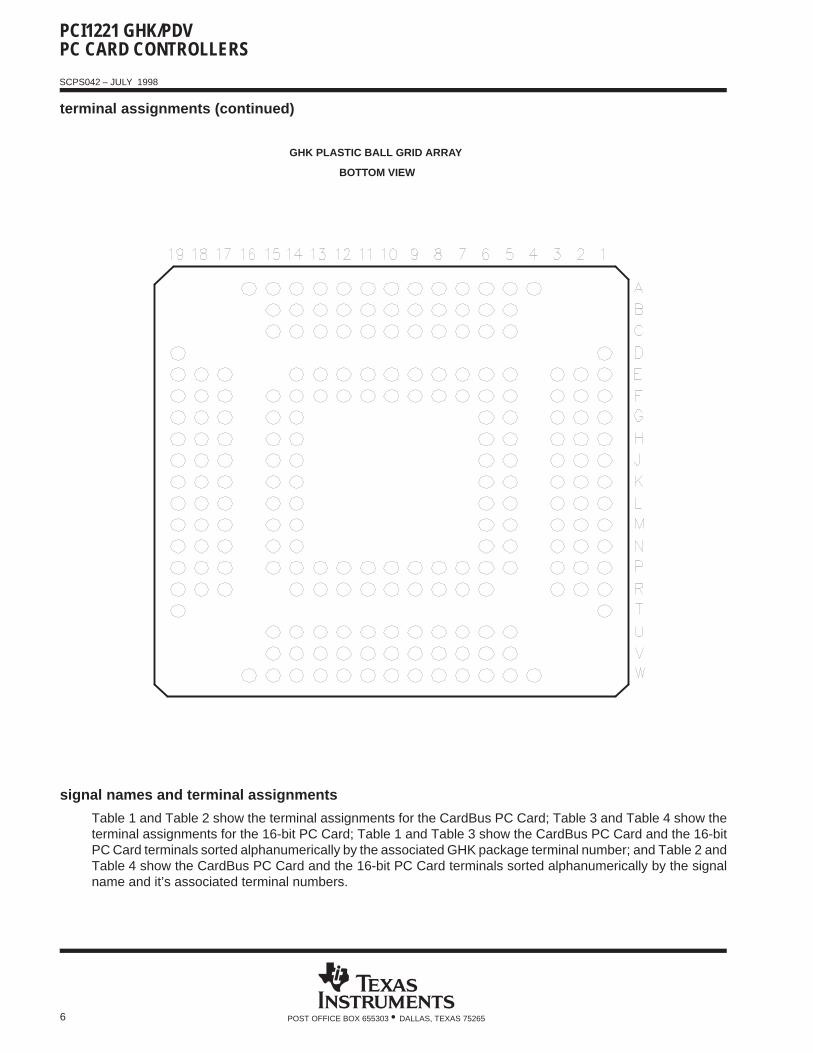
GHK PLASTIC BALL GRID ARRAY
BOTTOM VIEW
signal names and terminal assignments
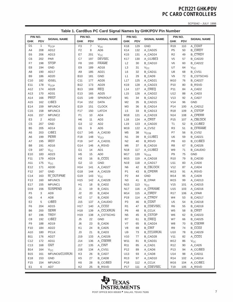
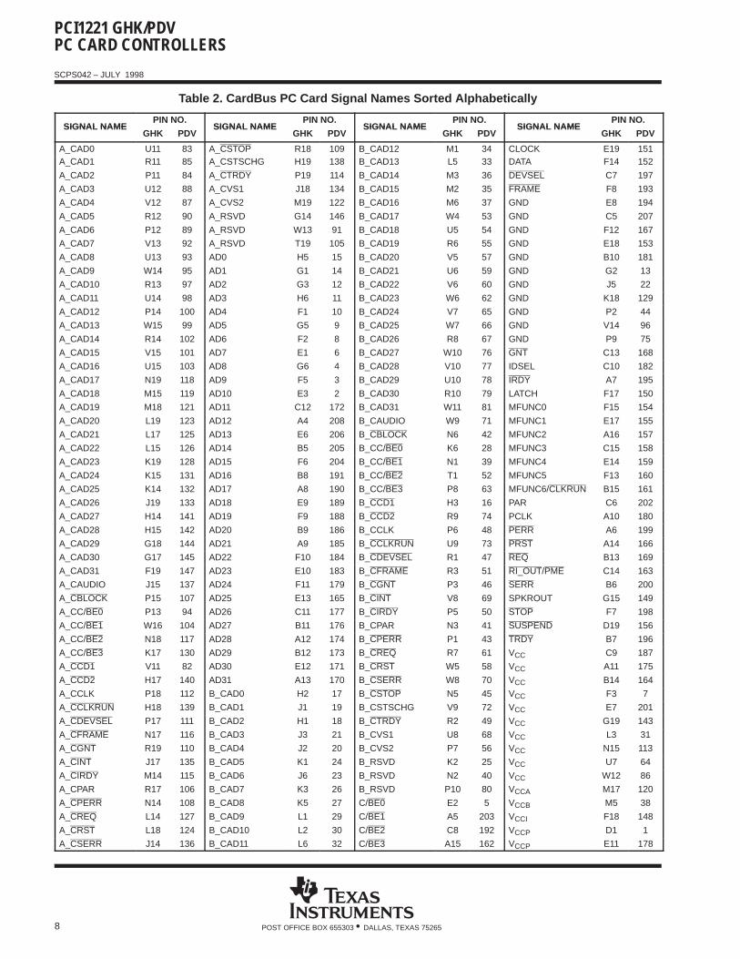
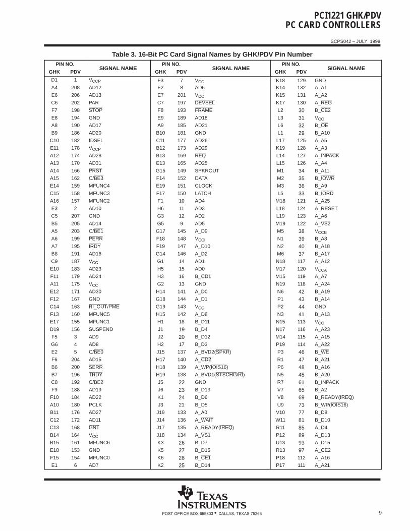
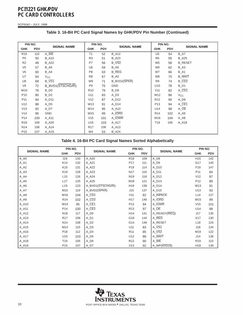
Table 1 and Table 2 show the terminal assignments for the CardBus PC Card; Table 3 and Table 4 show theterminal assignments for the 16-bit PC Card; Table 1 and Table 3 show the CardBus PC Card and the 16-bitPC Card terminals sorted alphanumerically by the associated GHK package terminal number; and Table 2 andTable 4 show the CardBus PC Card and the 16-bit PC Card terminals sorted alphanumerically by the signalname and it’s associated terminal numbers.
PCI1221 GHK/PDVPC CARD CONTROLLERS
SCPS042 – JULY 1998
7POST OFFICE BOX 655303 • DALLAS, TEXAS 75265
Table 1. CardBus PC Card Signal Names by GHK/PDV Pin NumberPIN NO.
SIGNAL NAMEPIN NO.
SIGNAL NAMEPIN NO.
SIGNAL NAMEPIN NO.
SIGNAL NAMEGHK PDV
SIGNAL NAMEGHK PDV
SIGNAL NAMEGHK PDV
SIGNAL NAMEGHK PDV
SIGNAL NAME
D1 1 VCCP F3 7 VCC K18 129 GND R19 110 A_CGNTA4 208 AD12 F2 8 AD6 K14 132 A_CAD25 P5 50 B_CIRDY
E6 206 AD13 E7 201 VCC K15 131 A_CAD24 R2 49 B_CTRDY
C6 202 PAR C7 197 DEVSEL K17 130 A_CC/BE3 V5 57 B_CAD20
F7 198 STOP F8 193 FRAME L2 30 B_CAD10 V6 60 B_CAD22
E8 194 GND E9 189 AD18 L3 31 VCC U7 64 VCC
A8 190 AD17 A9 185 AD21 L6 32 B_CAD11 U8 68 B_CVS1
B9 186 AD20 B10 181 GND L1 29 B_CAD9 V9 72 B_CSTSCHG
C10 182 IDSEL C11 177 AD26 L17 125 A_CAD21 W10 76 B_CAD27
E11 178 VCCP B12 173 AD29 K19 128 A_CAD23 P10 80 B_RSVD
A12 174 AD28 B13 169 REQ L14 127 A_CREQ P11 84 A_CAD2
A13 170 AD31 E13 165 AD25 L15 126 A_CAD22 U12 88 A_CAD3
A14 166 PRST G15 149 SPKROUT M1 34 B_CAD12 V13 92 A_CAD7
A15 162 C/BE3 F14 152 DATA M2 35 B_CAD15 V14 96 GND
E14 159 MFUNC4 E19 151 CLOCK M3 36 B_CAD14 P14 100 A_CAD12
C15 158 MFUNC3 F17 150 LATCH L5 33 B_CAD13 R18 109 A_CSTOP
A16 157 MFUNC2 F1 10 AD4 M18 121 A_CAD19 N14 108 A_CPERR
E3 2 AD10 H6 11 AD3 L18 124 A_CRST P15 107 A_CBLOCK
C5 207 GND G3 12 AD2 L19 123 A_CAD20 T1 52 B_CC/BE2
B5 205 AD14 G5 9 AD5 M19 122 A_CVS2 R3 51 B_CFRAME
A5 203 C/BE1 G17 145 A_CAD30 M5 38 VCCB P7 56 B_CVS2
A6 199 PERR F18 148 VCCI N1 39 B_CC/BE1 U6 59 B_CAD21
A7 195 IRDY F19 147 A_CAD31 N2 40 B_RSVD P8 63 B_CC/BE3
B8 191 AD16 G14 146 A_RSVD M6 37 B_CAD16 R8 67 B_CAD26
C9 187 VCC G1 14 AD1 N18 117 A_CC/BE2 W9 71 B_CAUDIO
E10 183 AD23 H5 15 AD0 M17 120 VCCA P9 75 GND
F11 179 AD24 H3 16 B_CCD1 M15 119 A_CAD18 R10 79 B_CAD30
A11 175 VCC G2 13 GND N19 118 A_CAD17 U11 83 A_CAD0
E12 171 AD30 H14 141 A_CAD27 N6 42 B_CBLOCK V12 87 A_CAD4
F12 167 GND G18 144 A_CAD29 P1 43 B_CPERR W13 91 A_RSVD
C14 163 RI_OUT/PME G19 143 VCC P2 44 GND W14 95 A_CAD9
F13 160 MFUNC5 H15 142 A_CAD28 N3 41 B_CPAR W15 99 A_CAD13
E17 155 MFUNC1 H1 18 B_CAD2 N15 113 VCC V15 101 A_CAD15
D19 156 SUSPEND J1 19 B_CAD1 N17 116 A_CFRAME U15 103 A_CAD16
F5 3 AD9 J2 20 B_CAD4 M14 115 A_CIRDY R17 106 A_CPAR
G6 4 AD8 H2 17 B_CAD0 P19 114 A_CTRDY W4 53 B_CAD17
E2 5 C/BE0 J15 137 A_CAUDIO P3 46 B_CGNT U5 54 B_CAD18
F6 204 AD15 H17 140 A_CCD2 R1 47 B_CDEVSEL R6 55 B_CAD19
B6 200 SERR H18 139 A_CCLKRUN P6 48 B_CCLK W5 58 B_CRST
B7 196 TRDY H19 138 A_CSTSCHG N5 45 B_CSTOP W6 62 B_CAD23
C8 192 C/BE2 J5 22 GND R7 61 B_CREQ W7 66 B_CAD25
F9 188 AD19 J6 23 B_CAD6 V7 65 B_CAD24 W8 70 B_CSERR
F10 184 AD22 K1 24 B_CAD5 V8 69 B_CINT R9 74 B_CCD2
A10 180 PCLK J3 21 B_CAD3 U9 73 B_CCLKRUN U10 78 B_CAD29
B11 176 AD27 J19 133 A_CAD26 V10 77 B_CAD28 V11 82 A_CCD1
C12 172 AD11 J14 136 A_CSERR W11 81 B_CAD31 W12 86 VCC
C13 168 GNT J17 135 A_CINT R11 85 A_CAD1 R12 90 A_CAD5
B14 164 VCC J18 134 A_CVS1 P12 89 A_CAD6 P13 94 A_CC/BE0
B15 161 MFUNC6/CLKRUN K3 26 B_CAD7 U13 93 A_CAD8 U14 98 A_CAD11
E18 153 GND K5 27 B_CAD8 R13 97 A_CAD10 R14 102 A_CAD14
F15 154 MFUNC0 K6 28 B_CC/BE0 P18 112 A_CCLK W16 104 A_CC/BE1
E1 6 AD7 K2 25 B_RSVD P17 111 A_CDEVSEL T19 105 A_RSVD
PCI1221 GHK/PDVPC CARD CONTROLLERS
SCPS042 – JULY 1998
8 POST OFFICE BOX 655303 • DALLAS, TEXAS 75265
Table 2. CardBus PC Card Signal Names Sorted Alphabetically
SIGNAL NAMEPIN NO.
SIGNAL NAMEPIN NO.
SIGNAL NAMEPIN NO.
SIGNAL NAMEPIN NO.
SIGNAL NAMEGHK PDV
SIGNAL NAMEGHK PDV
SIGNAL NAMEGHK PDV
SIGNAL NAMEGHK PDV
A_CAD0 U11 83 A_CSTOP R18 109 B_CAD12 M1 34 CLOCK E19 151A_CAD1 R11 85 A_CSTSCHG H19 138 B_CAD13 L5 33 DATA F14 152
A_CAD2 P11 84 A_CTRDY P19 114 B_CAD14 M3 36 DEVSEL C7 197
A_CAD3 U12 88 A_CVS1 J18 134 B_CAD15 M2 35 FRAME F8 193
A_CAD4 V12 87 A_CVS2 M19 122 B_CAD16 M6 37 GND E8 194
A_CAD5 R12 90 A_RSVD G14 146 B_CAD17 W4 53 GND C5 207
A_CAD6 P12 89 A_RSVD W13 91 B_CAD18 U5 54 GND F12 167
A_CAD7 V13 92 A_RSVD T19 105 B_CAD19 R6 55 GND E18 153
A_CAD8 U13 93 AD0 H5 15 B_CAD20 V5 57 GND B10 181
A_CAD9 W14 95 AD1 G1 14 B_CAD21 U6 59 GND G2 13
A_CAD10 R13 97 AD2 G3 12 B_CAD22 V6 60 GND J5 22
A_CAD11 U14 98 AD3 H6 11 B_CAD23 W6 62 GND K18 129
A_CAD12 P14 100 AD4 F1 10 B_CAD24 V7 65 GND P2 44
A_CAD13 W15 99 AD5 G5 9 B_CAD25 W7 66 GND V14 96
A_CAD14 R14 102 AD6 F2 8 B_CAD26 R8 67 GND P9 75
A_CAD15 V15 101 AD7 E1 6 B_CAD27 W10 76 GNT C13 168
A_CAD16 U15 103 AD8 G6 4 B_CAD28 V10 77 IDSEL C10 182
A_CAD17 N19 118 AD9 F5 3 B_CAD29 U10 78 IRDY A7 195
A_CAD18 M15 119 AD10 E3 2 B_CAD30 R10 79 LATCH F17 150
A_CAD19 M18 121 AD11 C12 172 B_CAD31 W11 81 MFUNC0 F15 154
A_CAD20 L19 123 AD12 A4 208 B_CAUDIO W9 71 MFUNC1 E17 155
A_CAD21 L17 125 AD13 E6 206 B_CBLOCK N6 42 MFUNC2 A16 157
A_CAD22 L15 126 AD14 B5 205 B_CC/BE0 K6 28 MFUNC3 C15 158
A_CAD23 K19 128 AD15 F6 204 B_CC/BE1 N1 39 MFUNC4 E14 159
A_CAD24 K15 131 AD16 B8 191 B_CC/BE2 T1 52 MFUNC5 F13 160
A_CAD25 K14 132 AD17 A8 190 B_CC/BE3 P8 63 MFUNC6/CLKRUN B15 161
A_CAD26 J19 133 AD18 E9 189 B_CCD1 H3 16 PAR C6 202
A_CAD27 H14 141 AD19 F9 188 B_CCD2 R9 74 PCLK A10 180
A_CAD28 H15 142 AD20 B9 186 B_CCLK P6 48 PERR A6 199
A_CAD29 G18 144 AD21 A9 185 B_CCLKRUN U9 73 PRST A14 166
A_CAD30 G17 145 AD22 F10 184 B_CDEVSEL R1 47 REQ B13 169
A_CAD31 F19 147 AD23 E10 183 B_CFRAME R3 51 RI_OUT/PME C14 163
A_CAUDIO J15 137 AD24 F11 179 B_CGNT P3 46 SERR B6 200
A_CBLOCK P15 107 AD25 E13 165 B_CINT V8 69 SPKROUT G15 149
A_CC/BE0 P13 94 AD26 C11 177 B_CIRDY P5 50 STOP F7 198
A_CC/BE1 W16 104 AD27 B11 176 B_CPAR N3 41 SUSPEND D19 156
A_CC/BE2 N18 117 AD28 A12 174 B_CPERR P1 43 TRDY B7 196
A_CC/BE3 K17 130 AD29 B12 173 B_CREQ R7 61 VCC C9 187
A_CCD1 V11 82 AD30 E12 171 B_CRST W5 58 VCC A11 175
A_CCD2 H17 140 AD31 A13 170 B_CSERR W8 70 VCC B14 164
A_CCLK P18 112 B_CAD0 H2 17 B_CSTOP N5 45 VCC F3 7
A_CCLKRUN H18 139 B_CAD1 J1 19 B_CSTSCHG V9 72 VCC E7 201
A_CDEVSEL P17 111 B_CAD2 H1 18 B_CTRDY R2 49 VCC G19 143
A_CFRAME N17 116 B_CAD3 J3 21 B_CVS1 U8 68 VCC L3 31
A_CGNT R19 110 B_CAD4 J2 20 B_CVS2 P7 56 VCC N15 113
A_CINT J17 135 B_CAD5 K1 24 B_RSVD K2 25 VCC U7 64
A_CIRDY M14 115 B_CAD6 J6 23 B_RSVD N2 40 VCC W12 86
A_CPAR R17 106 B_CAD7 K3 26 B_RSVD P10 80 VCCA M17 120
A_CPERR N14 108 B_CAD8 K5 27 C/BE0 E2 5 VCCB M5 38
A_CREQ L14 127 B_CAD9 L1 29 C/BE1 A5 203 VCCI F18 148
A_CRST L18 124 B_CAD10 L2 30 C/BE2 C8 192 VCCP D1 1
A_CSERR J14 136 B_CAD11 L6 32 C/BE3 A15 162 VCCP E11 178
PCI1221 GHK/PDVPC CARD CONTROLLERS
SCPS042 – JULY 1998
9POST OFFICE BOX 655303 • DALLAS, TEXAS 75265
Table 3. 16-Bit PC Card Signal Names by GHK/PDV Pin NumberPIN NO.
SIGNAL NAMEPIN NO.
SIGNAL NAMEPIN NO.
SIGNAL NAMEGHK PDV
SIGNAL NAMEGHK PDV
SIGNAL NAMEGHK PDV
SIGNAL NAME
D1 1 VCCP F3 7 VCC K18 129 GNDA4 208 AD12 F2 8 AD6 K14 132 A_A1
E6 206 AD13 E7 201 VCC K15 131 A_A2
C6 202 PAR C7 197 DEVSEL K17 130 A_REG
F7 198 STOP F8 193 FRAME L2 30 B_CE2
E8 194 GND E9 189 AD18 L3 31 VCC
A8 190 AD17 A9 185 AD21 L6 32 B_OE
B9 186 AD20 B10 181 GND L1 29 B_A10
C10 182 IDSEL C11 177 AD26 L17 125 A_A5
E11 178 VCCP B12 173 AD29 K19 128 A_A3
A12 174 AD28 B13 169 REQ L14 127 A_INPACK
A13 170 AD31 E13 165 AD25 L15 126 A_A4
A14 166 PRST G15 149 SPKROUT M1 34 B_A11
A15 162 C/BE3 F14 152 DATA M2 35 B_IOWR
E14 159 MFUNC4 E19 151 CLOCK M3 36 B_A9
C15 158 MFUNC3 F17 150 LATCH L5 33 B_IORD
A16 157 MFUNC2 F1 10 AD4 M18 121 A_A25
E3 2 AD10 H6 11 AD3 L18 124 A_RESET
C5 207 GND G3 12 AD2 L19 123 A_A6
B5 205 AD14 G5 9 AD5 M19 122 A_VS2
A5 203 C/BE1 G17 145 A_D9 M5 38 VCCB
A6 199 PERR F18 148 VCCI N1 39 B_A8
A7 195 IRDY F19 147 A_D10 N2 40 B_A18
B8 191 AD16 G14 146 A_D2 M6 37 B_A17
C9 187 VCC G1 14 AD1 N18 117 A_A12
E10 183 AD23 H5 15 AD0 M17 120 VCCA
F11 179 AD24 H3 16 B_CD1 M15 119 A_A7
A11 175 VCC G2 13 GND N19 118 A_A24
E12 171 AD30 H14 141 A_D0 N6 42 B_A19
F12 167 GND G18 144 A_D1 P1 43 B_A14
C14 163 RI_OUT/PME G19 143 VCC P2 44 GND
F13 160 MFUNC5 H15 142 A_D8 N3 41 B_A13
E17 155 MFUNC1 H1 18 B_D11 N15 113 VCC
D19 156 SUSPEND J1 19 B_D4 N17 116 A_A23
F5 3 AD9 J2 20 B_D12 M14 115 A_A15
G6 4 AD8 H2 17 B_D3 P19 114 A_A22
E2 5 C/BE0 J15 137 A_BVD2(SPKR) P3 46 B_WE
F6 204 AD15 H17 140 A_CD2 R1 47 B_A21
B6 200 SERR H18 139 A_WP(IOIS16) P6 48 B_A16
B7 196 TRDY H19 138 A_BVD1(STSCHG/RI) N5 45 B_A20
C8 192 C/BE2 J5 22 GND R7 61 B_INPACK
F9 188 AD19 J6 23 B_D13 V7 65 B_A2
F10 184 AD22 K1 24 B_D6 V8 69 B_READY(IREQ)
A10 180 PCLK J3 21 B_D5 U9 73 B_WP(IOIS16)
B11 176 AD27 J19 133 A_A0 V10 77 B_D8
C12 172 AD11 J14 136 A_WAIT W11 81 B_D10
C13 168 GNT J17 135 A_READY(IREQ) R11 85 A_D4
B14 164 VCC J18 134 A_VS1 P12 89 A_D13
B15 161 MFUNC6 K3 26 B_D7 U13 93 A_D15
E18 153 GND K5 27 B_D15 R13 97 A_CE2
F15 154 MFUNC0 K6 28 B_CE1 P18 112 A_A16
E1 6 AD7 K2 25 B_D14 P17 111 A_A21
PCI1221 GHK/PDVPC CARD CONTROLLERS
SCPS042 – JULY 1998
10 POST OFFICE BOX 655303 • DALLAS, TEXAS 75265
Table 3. 16-Bit PC Card Signal Names by GHK/PDV Pin Number (Continued)
PIN NO.SIGNAL NAME
PIN NO.SIGNAL NAME
PIN NO.SIGNAL NAME
GHK PDVSIGNAL NAME
GHK PDVSIGNAL NAME
GHK PDVSIGNAL NAME
R19 110 A_WE T1 52 B_A12 U5 54 B_A7P5 50 B_A15 R3 51 B_A23 R6 55 B_A25
R2 49 B_A22 P7 56 B_VS2 W5 58 B_RESET
V5 57 B_A6 U6 59 B_A5 W6 62 B_A3
V6 60 B_A4 P8 63 B_REG W7 66 B_A1
U7 64 VCC R8 67 B_A0 W8 70 B_WAIT
U8 68 B_VS1 W9 71 B_BVD2(SPKR) R9 74 B_CD2
V9 72 B_BVD1(STSCHG/RI) P9 75 GND U10 78 B_D1
W10 76 B_D0 R10 79 B_D9 V11 82 A_CD1
P10 80 B_D2 U11 83 A_D3 W12 86 VCC
P11 84 A_D11 V12 87 A_D12 R12 90 A_D6
U12 88 A_D5 W13 91 A_D14 P13 94 A_CE1
V13 92 A_D7 W14 95 A_A10 U14 98 A_OE
V14 96 GND W15 99 A_IORD R14 102 A_A9
P14 100 A_A11 V15 101 A_IOWR W16 104 A_A8
R18 109 A_A20 U15 103 A_A17 T19 105 A_A18
N14 108 A_A14 R17 106 A_A13
P15 107 A_A19 W4 53 B_A24
Table 4. 16-Bit PC Card Signal Names Sorted Alphabetically
SIGNAL NAMEPIN NO.
SIGNAL NAMEPIN NO.
SIGNAL NAMEPIN NO.
SIGNAL NAMEGHK PDV
SIGNAL NAMEGHK PDV
SIGNAL NAMEGHK PDV
A_A0 J19 133 A_A20 R18 109 A_D8 H15 142A_A1 K14 132 A_A21 P17 111 A_D9 G17 145
A_A2 K15 131 A_A22 P19 114 A_D10 F19 147
A_A3 K19 128 A_A23 N17 116 A_D11 P11 84A_A4 L15 126 A_A24 N19 118 A_D12 V12 87A_A5 L17 125 A_A25 M18 121 A_D13 P12 89A_A6 L19 123 A_BVD1(STSCHG/RI) H19 138 A_D14 W13 91A_A7 M15 119 A_BVD2(SPKR) J15 137 A_D15 U13 93A_A8 W16 104 A_CD1 V11 82 A_INPACK L14 127
A_A9 R14 102 A_CD2 H17 140 A_IORD W15 99A_A10 W14 95 A_CE1 P13 94 A_IOWR V15 101A_A11 P14 100 A_CE2 R13 97 A_OE U14 98A_A12 N18 117 A_D0 H14 141 A_READY(IREQ) J17 135
A_A13 R17 106 A_D1 G18 144 A_REG K17 130
A_A14 N14 108 A_D2 G14 146 A_RESET L18 124
A_A15 M14 115 A_D3 U11 83 A_VS1 J18 134
A_A16 P18 112 A_D4 R11 85 A_VS2 M19 122
A_A17 U15 103 A_D5 U12 88 A_WAIT J14 136
A_A18 T19 105 A_D6 R12 90 A_WE R19 110
A_A19 P15 107 A_D7 V13 92 A_WP(IOIS16) H18 139
PCI1221 GHK/PDVPC CARD CONTROLLERS
SCPS042 – JULY 1998
11POST OFFICE BOX 655303 • DALLAS, TEXAS 75265
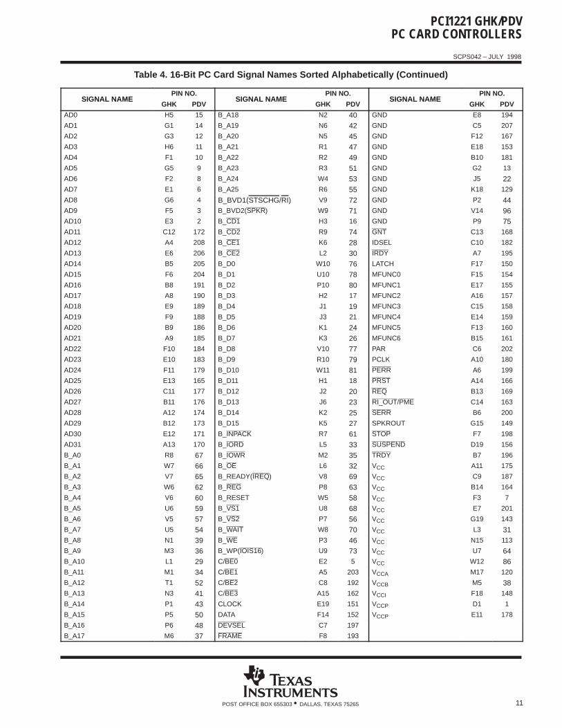
Table 4. 16-Bit PC Card Signal Names Sorted Alphabetically (Continued)
SIGNAL NAMEPIN NO.
SIGNAL NAMEPIN NO.
SIGNAL NAMEPIN NO.
SIGNAL NAMEGHK PDV
SIGNAL NAMEGHK PDV
SIGNAL NAMEGHK PDV
AD0 H5 15 B_A18 N2 40 GND E8 194
AD1 G1 14 B_A19 N6 42 GND C5 207
AD2 G3 12 B_A20 N5 45 GND F12 167
AD3 H6 11 B_A21 R1 47 GND E18 153
AD4 F1 10 B_A22 R2 49 GND B10 181
AD5 G5 9 B_A23 R3 51 GND G2 13
AD6 F2 8 B_A24 W4 53 GND J5 22AD7 E1 6 B_A25 R6 55 GND K18 129
AD8 G6 4 B_BVD1(STSCHG/RI) V9 72 GND P2 44AD9 F5 3 B_BVD2(SPKR) W9 71 GND V14 96AD10 E3 2 B_CD1 H3 16 GND P9 75AD11 C12 172 B_CD2 R9 74 GNT C13 168
AD12 A4 208 B_CE1 K6 28 IDSEL C10 182
AD13 E6 206 B_CE2 L2 30 IRDY A7 195
AD14 B5 205 B_D0 W10 76 LATCH F17 150
AD15 F6 204 B_D1 U10 78 MFUNC0 F15 154
AD16 B8 191 B_D2 P10 80 MFUNC1 E17 155
AD17 A8 190 B_D3 H2 17 MFUNC2 A16 157
AD18 E9 189 B_D4 J1 19 MFUNC3 C15 158
AD19 F9 188 B_D5 J3 21 MFUNC4 E14 159
AD20 B9 186 B_D6 K1 24 MFUNC5 F13 160
AD21 A9 185 B_D7 K3 26 MFUNC6 B15 161
AD22 F10 184 B_D8 V10 77 PAR C6 202
AD23 E10 183 B_D9 R10 79 PCLK A10 180
AD24 F11 179 B_D10 W11 81 PERR A6 199
AD25 E13 165 B_D11 H1 18 PRST A14 166
AD26 C11 177 B_D12 J2 20 REQ B13 169
AD27 B11 176 B_D13 J6 23 RI_OUT/PME C14 163
AD28 A12 174 B_D14 K2 25 SERR B6 200
AD29 B12 173 B_D15 K5 27 SPKROUT G15 149
AD30 E12 171 B_INPACK R7 61 STOP F7 198
AD31 A13 170 B_IORD L5 33 SUSPEND D19 156
B_A0 R8 67 B_IOWR M2 35 TRDY B7 196
B_A1 W7 66 B_OE L6 32 VCC A11 175
B_A2 V7 65 B_READY(IREQ) V8 69 VCC C9 187
B_A3 W6 62 B_REG P8 63 VCC B14 164
B_A4 V6 60 B_RESET W5 58 VCC F3 7
B_A5 U6 59 B_VS1 U8 68 VCC E7 201
B_A6 V5 57 B_VS2 P7 56 VCC G19 143
B_A7 U5 54 B_WAIT W8 70 VCC L3 31B_A8 N1 39 B_WE P3 46 VCC N15 113
B_A9 M3 36 B_WP(IOIS16) U9 73 VCC U7 64B_A10 L1 29 C/BE0 E2 5 VCC W12 86B_A11 M1 34 C/BE1 A5 203 VCCA M17 120
B_A12 T1 52 C/BE2 C8 192 VCCB M5 38B_A13 N3 41 C/BE3 A15 162 VCCI F18 148
B_A14 P1 43 CLOCK E19 151 VCCP D1 1
B_A15 P5 50 DATA F14 152 VCCP E11 178
B_A16 P6 48 DEVSEL C7 197
B_A17 M6 37 FRAME F8 193
PCI1221 GHK/PDVPC CARD CONTROLLERS
SCPS042 – JULY 1998
12 POST OFFICE BOX 655303 • DALLAS, TEXAS 75265
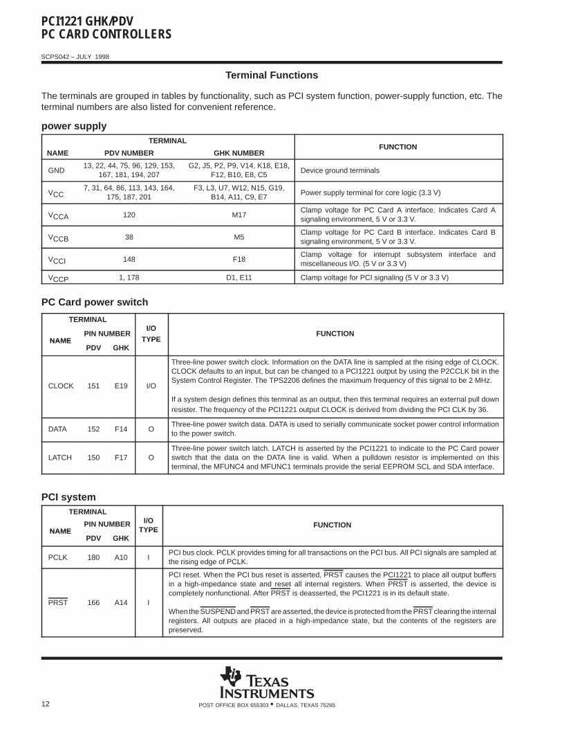
Terminal Functions
The terminals are grouped in tables by functionality, such as PCI system function, power-supply function, etc. Theterminal numbers are also listed for convenient reference.
power supplyTERMINAL
FUNCTIONNAME PDV NUMBER GHK NUMBER
FUNCTION
GND13, 22, 44, 75, 96, 129, 153,
167, 181, 194, 207G2, J5, P2, P9, V14, K18, E18,
F12, B10, E8, C5Device ground terminals
VCC7, 31, 64, 86, 113, 143, 164,
175, 187, 201F3, L3, U7, W12, N15, G19,
B14, A11, C9, E7Power supply terminal for core logic (3.3 V)
VCCA 120 M17Clamp voltage for PC Card A interface. Indicates Card Asignaling environment, 5 V or 3.3 V.
VCCB 38 M5Clamp voltage for PC Card B interface. Indicates Card Bsignaling environment, 5 V or 3.3 V.
VCCI 148 F18Clamp voltage for interrupt subsystem interface andmiscellaneous I/O. (5 V or 3.3 V)
VCCP 1, 178 D1, E11 Clamp voltage for PCI signaling (5 V or 3.3 V)
PC Card power switch
TERMINALI/O
NAMEPIN NUMBER
I/O
TYPEFUNCTION
NAMEPDV GHK
TYPE
CLOCK 151 E19 I/O
Three-line power switch clock. Information on the DATA line is sampled at the rising edge of CLOCK.CLOCK defaults to an input, but can be changed to a PCI1221 output by using the P2CCLK bit in theSystem Control Register. The TPS2206 defines the maximum frequency of this signal to be 2 MHz.
If a system design defines this terminal as an output, then this terminal requires an external pull downresister. The frequency of the PCI1221 output CLOCK is derived from dividing the PCI CLK by 36.
DATA 152 F14 OThree-line power switch data. DATA is used to serially communicate socket power control informationto the power switch.
LATCH 150 F17 OThree-line power switch latch. LATCH is asserted by the PCI1221 to indicate to the PC Card powerswitch that the data on the DATA line is valid. When a pulldown resistor is implemented on thisterminal, the MFUNC4 and MFUNC1 terminals provide the serial EEPROM SCL and SDA interface.
PCI systemTERMINAL
NAMEPIN NUMBER I/O
TYPEFUNCTION
NAMEPDV GHK
TYPE
PCLK 180 A10 IPCI bus clock. PCLK provides timing for all transactions on the PCI bus. All PCI signals are sampled atthe rising edge of PCLK.
PRST 166 A14 I
PCI reset. When the PCI bus reset is asserted, PRST causes the PCI1221 to place all output buffersin a high-impedance state and reset all internal registers. When PRST is asserted, the device iscompletely nonfunctional. After PRST is deasserted, the PCI1221 is in its default state.
When the SUSPEND and PRST are asserted, the device is protected from the PRST clearing the internalregisters. All outputs are placed in a high-impedance state, but the contents of the registers arepreserved.
PCI1221 GHK/PDVPC CARD CONTROLLERS
SCPS042 – JULY 1998
13POST OFFICE BOX 655303 • DALLAS, TEXAS 75265
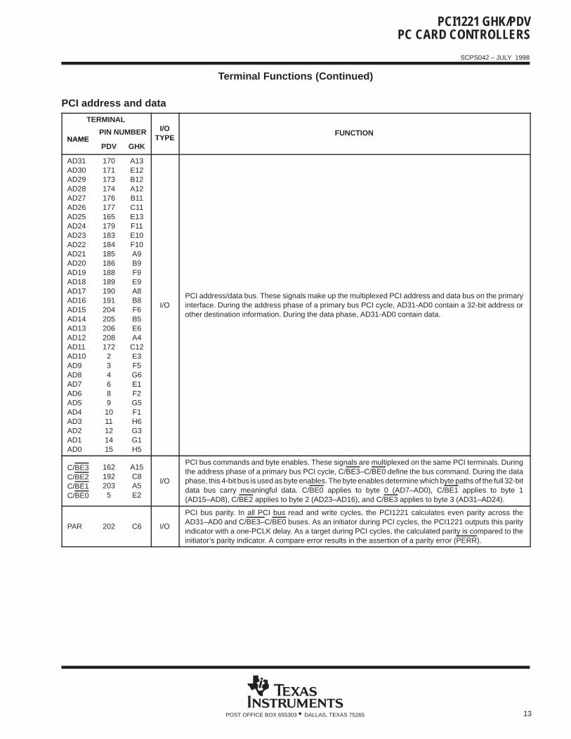
Terminal Functions (Continued)
PCI address and data
TERMINAL
NAMEPIN NUMBER I/O
TYPEFUNCTION
NAMEPDV GHK
TYPE
AD31AD30AD29AD28AD27AD26AD25AD24AD23AD22AD21AD20AD19AD18AD17AD16AD15AD14AD13AD12AD11AD10AD9AD8AD7AD6AD5AD4AD3AD2AD1AD0
1701711731741761771651791831841851861881891901912042052062081722346891011121415
A13E12B12A12B11C11E13F11E10F10A9B9F9E9A8B8F6B5E6A4
C12E3F5G6E1F2G5F1H6G3G1H5
I/OPCI address/data bus. These signals make up the multiplexed PCI address and data bus on the primaryinterface. During the address phase of a primary bus PCI cycle, AD31-AD0 contain a 32-bit address orother destination information. During the data phase, AD31-AD0 contain data.
C/BE3C/BE2C/BE1C/BE0
1621922035
A15C8A5E2
I/O
PCI bus commands and byte enables. These signals are multiplexed on the same PCI terminals. Duringthe address phase of a primary bus PCI cycle, C/BE3–C/BE0 define the bus command. During the dataphase, this 4-bit bus is used as byte enables. The byte enables determine which byte paths of the full 32-bitdata bus carry meaningful data. C/BE0 applies to byte 0 (AD7–AD0), C/BE1 applies to byte 1(AD15–AD8), C/BE2 applies to byte 2 (AD23–AD16), and C/BE3 applies to byte 3 (AD31–AD24).
PAR 202 C6 I/O
PCI bus parity. In all PCI bus read and write cycles, the PCI1221 calculates even parity across theAD31–AD0 and C/BE3–C/BE0 buses. As an initiator during PCI cycles, the PCI1221 outputs this parityindicator with a one-PCLK delay. As a target during PCI cycles, the calculated parity is compared to theinitiator’s parity indicator. A compare error results in the assertion of a parity error (PERR).
PCI1221 GHK/PDVPC CARD CONTROLLERS
SCPS042 – JULY 1998
14 POST OFFICE BOX 655303 • DALLAS, TEXAS 75265
Terminal Functions (Continued)
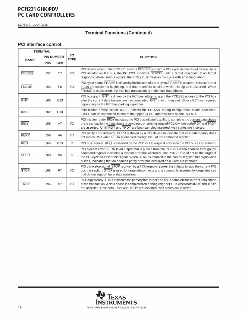
PCI interface control
TERMINAL
NAMEPIN NUMBER I/O
TYPEFUNCTION
NAMEPDV GHK
TYPE
DEVSEL 197 C7 I/OPCI device select. The PCI1221 asserts DEVSEL to claim a PCI cycle as the target device. As aPCI initiator on the bus, the PCI1221 monitors DEVSEL until a target responds. If no targetresponds before timeout occurs, the PCI1221 terminates the cycle with an initiator abort.
FRAME 193 F8 I/OPCI cycle frame. FRAME is driven by the initiator of a bus cycle. FRAME is asserted to indicate thata bus transaction is beginning, and data transfers continue while this signal is asserted. WhenFRAME is deasserted, the PCI bus transaction is in the final data phase.
GNT 168 C13 IPCI bus grant. GNT is driven by the PCI bus arbiter to grant the PCI1221 access to the PCI busafter the current data transaction has completed. GNT may or may not follow a PCI bus request,depending on the PCI bus parking algorithm.
IDSEL 182 C10 IInitialization device select. IDSEL selects the PCI1221 during configuration space accesses.IDSEL can be connected to one of the upper 24 PCI address lines on the PCI bus.
IRDY 195 A7 I/OPCI initiator ready. IRDY indicates the PCI bus initiator’s ability to complete the current data phaseof the transaction. A data phase is completed on a rising edge of PCLK where both IRDY and TRDYare asserted. Until IRDY and TRDY are both sampled asserted, wait states are inserted.
PERR 199 A6 I/OPCI parity error indicator. PERR is driven by a PCI device to indicate that calculated parity doesnot match PAR when PERR is enabled through bit 6 of the command register.
REQ 169 B13 O PCI bus request. REQ is asserted by the PCI1221 to request access to the PCI bus as an initiator.
SERR 200 B6 O
PCI system error. SERR is an output that is pulsed from the PCI1221 when enabled through thecommand register indicating a system error has occurred. The PCI1221 need not be the target ofthe PCI cycle to assert this signal. When SERR is enabled in the control register, this signal alsopulses, indicating that an address parity error has occurred on a CardBus interface.
STOP 198 F7 I/OPCI cycle stop signal. STOP is driven by a PCI target to request the initiator to stop the current PCIbus transaction. STOP is used for target disconnects and is commonly asserted by target devicesthat do not support burst data transfers.
TRDY 196 B7 I/OPCI target ready. TRDY indicates the primary bus target’s ability to complete the current data phaseof the transaction. A data phase is completed on a rising edge of PCLK when both IRDY and TRDYare asserted. Until both IRDY and TRDY are asserted, wait states are inserted.
PCI1221 GHK/PDVPC CARD CONTROLLERS
SCPS042 – JULY 1998
15POST OFFICE BOX 655303 • DALLAS, TEXAS 75265
Terminal Functions (Continued)
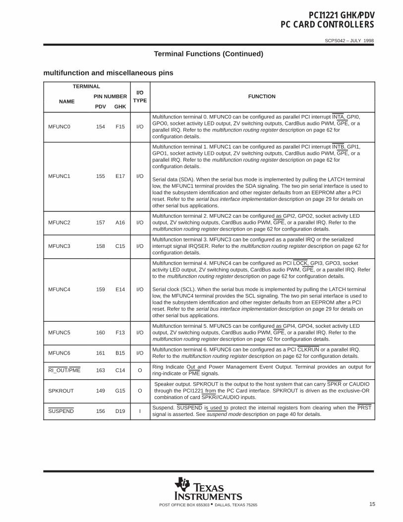
multifunction and miscellaneous pins
TERMINALI/O
NAMEPIN NUMBER
I/O
TYPEFUNCTION
NAMEPDV GHK
TYPE
MFUNC0 154 F15 I/O
Multifunction terminal 0. MFUNC0 can be configured as parallel PCI interrupt INTA, GPI0,GPO0, socket activity LED output, ZV switching outputs, CardBus audio PWM, GPE, or aparallel IRQ. Refer to the multifunction routing register description on page 62 forconfiguration details.
MFUNC1 155 E17 I/O
Multifunction terminal 1. MFUNC1 can be configured as parallel PCI interrupt INTB, GPI1,GPO1, socket activity LED output, ZV switching outputs, CardBus audio PWM, GPE, or aparallel IRQ. Refer to the multifunction routing register description on page 62 forconfiguration details.
Serial data (SDA). When the serial bus mode is implemented by pulling the LATCH terminallow, the MFUNC1 terminal provides the SDA signaling. The two pin serial interface is used toload the subsystem identification and other register defaults from an EEPROM after a PCIreset. Refer to the serial bus interface implementation description on page 29 for details onother serial bus applications.
MFUNC2 157 A16 I/OMultifunction terminal 2. MFUNC2 can be configured as GPI2, GPO2, socket activity LEDoutput, ZV switching outputs, CardBus audio PWM, GPE, or a parallel IRQ. Refer to themultifunction routing register description on page 62 for configuration details.
MFUNC3 158 C15 I/OMultifunction terminal 3. MFUNC3 can be configured as a parallel IRQ or the serializedinterrupt signal IRQSER. Refer to the multifunction routing register description on page 62 forconfiguration details.
MFUNC4 159 E14 I/O
Multifunction terminal 4. MFUNC4 can be configured as PCI LOCK, GPI3, GPO3, socketactivity LED output, ZV switching outputs, CardBus audio PWM, GPE, or a parallel IRQ. Referto the multifunction routing register description on page 62 for configuration details.
Serial clock (SCL). When the serial bus mode is implemented by pulling the LATCH terminallow, the MFUNC4 terminal provides the SCL signaling. The two pin serial interface is used toload the subsystem identification and other register defaults from an EEPROM after a PCIreset. Refer to the serial bus interface implementation description on page 29 for details onother serial bus applications.
MFUNC5 160 F13 I/OMultifunction terminal 5. MFUNC5 can be configured as GPI4, GPO4, socket activity LEDoutput, ZV switching outputs, CardBus audio PWM, GPE, or a parallel IRQ. Refer to themultifunction routing register description on page 62 for configuration details.
MFUNC6 161 B15 I/OMultifunction terminal 6. MFUNC6 can be configured as a PCI CLKRUN or a parallel IRQ.Refer to the multifunction routing register description on page 62 for configuration details.
RI_OUT/PME 163 C14 ORing Indicate Out and Power Management Event Output. Terminal provides an output forring-indicate or PME signals.
SPKROUT 149 G15 OSpeaker output. SPKROUT is the output to the host system that can carry SPKR or CAUDIOthrough the PCI1221 from the PC Card interface. SPKROUT is driven as the exclusive-ORcombination of card SPKR//CAUDIO inputs.
SUSPEND 156 D19 ISuspend. SUSPEND is used to protect the internal registers from clearing when the PRSTsignal is asserted. See suspend mode description on page 40 for details.
PCI1221 GHK/PDVPC CARD CONTROLLERS
SCPS042 – JULY 1998
16 POST OFFICE BOX 655303 • DALLAS, TEXAS 75265
Terminal Functions (Continued)
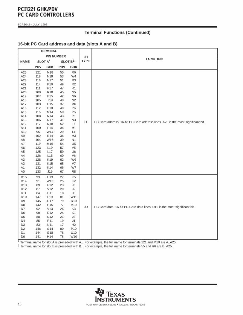
16-bit PC Card address and data (slots A and B)
TERMINAL
PIN NUMBER I/OFUNCTION
NAME SLOT A† SLOT B‡ TYPEFUNCTION
PDV GHK PDV GHK
A25A24A23A22A21A20A19A18A17A16A15A14A13A12A11A10A9A8A7A6A5A4A3A2A1A0
12111811611411110910710510311211510810611710095102104119123125126128131132133
M18N19N17P19P17R18P15T19U15P18M14N14R17N18P14W14R14W16M15L19L17L15K19K15K14J19
5553514947454240374850434152342936395457596062656667
R6W4R3R2R1N5N6N2M6P6P5P1N3T1M1L1M3N1U5V5U6V6W6V7W7R8
O PC Card address. 16-bit PC Card address lines. A25 is the most-significant bit.
D15D14D13D12D11D10D9D8D7D6D5D4D3D2D1D0
93918987841471451429290888583146144141
U13W13P12V12P11F19G17H15V13R12U12R11U11G14G18H14
27252320188179772624211917807876
K5K2J6J2H1
W11R10V10K3K1J3J1H2P10U10W10
I/O PC Card data. 16-bit PC Card data lines. D15 is the most-significant bit.
† Terminal name for slot A is preceded with A_. For example, the full name for terminals 121 and M18 are A_A25.‡ Terminal name for slot B is preceded with B_. For example, the full name for terminals 55 and R6 are B_A25.
PCI1221 GHK/PDVPC CARD CONTROLLERS
SCPS042 – JULY 1998
17POST OFFICE BOX 655303 • DALLAS, TEXAS 75265
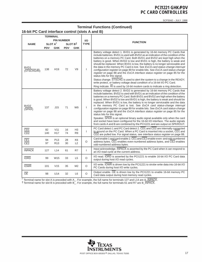
Terminal Functions (Continued)16-bit PC Card interface control (slots A and B)
TERMINALPIN NUMBER I/O
FUNCTIONNAME SLOT A† SLOT B‡ TYPE
FUNCTION
PDV GHK PDV GHK
BVD1(STSCHG/RI)
138 H19 72 V9 I
Battery voltage detect 1. BVD1 is generated by 16-bit memory PC Cards thatinclude batteries. BVD1 is used with BVD2 as an indication of the condition of thebatteries on a memory PC Card. Both BVD1 and BVD2 are kept high when thebattery is good. When BVD2 is low and BVD1 is high, the battery is weak andshould be replaced. When BVD1 is low, the battery is no longer serviceable andthe data in the memory PC Card is lost. See ExCA card status-change interruptconfiguration register on page 89 for enable bits. See ExCA card status-changeregister on page 88 and the ExCA interface status register on page 85 for thestatus bits for this signal.Status change. STSCHG is used to alert the system to a change in the READY,write protect, or battery voltage dead condition of a 16-bit I/O PC Card.Ring indicate. RI is used by 16-bit modem cards to indicate a ring detection.
BVD2(SPKR)
137 J15 71 W9 I
Battery voltage detect 2. BVD2 is generated by 16-bit memory PC Cards thatinclude batteries. BVD2 is used with BVD1 as an indication of the condition of thebatteries on a memory PC Card. Both BVD1 and BVD2 are high when the batteryis good. When BVD2 is low and BVD1 is high, the battery is weak and should bereplaced. When BVD1 is low, the battery is no longer serviceable and the datain the memory PC Card is lost. See ExCA card status-change interruptconfiguration register on page 89 for enable bits. See ExCA card status-changeregister on page 88 and the ExCA interface status register on page 85 for thestatus bits for this signal.Speaker. SPKR is an optional binary audio signal available only when the cardand socket have been configured for the 16-bit I/O interface. The audio signalsfrom cards A and B are combined by the PCI1221 and are output on SPKROUT.
CD1CD2
82140
V11H17
1674
H3R9
IPC Card detect 1 and PC Card detect 2. CD1 and CD2 are internally connectedto ground on the PC Card. When a PC Card is inserted into a socket, CD1 andCD2 are pulled low. For signal status, see interface status register on page 88.
CE1CE2
9497
P13R13
2830
K6L2
OCard enable 1 and card enable 2. CE1 and CE2 enable even- and odd-numberedaddress bytes. CE1 enables even-numbered address bytes, and CE2 enablesodd-numbered address bytes.
INPACK 127 L14 61 R7 IInput acknowledge. INPACK is asserted by the PC Card when it can respond toan I/O read cycle at the current address.
IORD 99 W15 33 L5 OI/O read. IORD is asserted by the PCI1221 to enable 16-bit I/O PC Card dataoutput during host I/O read cycles.
IOWR 101 V15 35 M2 OI/O write. IOWR is driven low by the PCI1221 to strobe write data into 16-bit I/OPC Cards during host I/O write cycles.
OE 98 U14 32 L6 OOutput enable. OE is driven low by the PCI1221 to enable 16-bit memory PCCard data output during host memory read cycles.
† Terminal name for slot A is preceded with A_. For example, the full name for terminals 127 and L14 are A_INPACK.‡ Terminal name for slot B is preceded with B_. For example, the full name for terminals 61 and R7 are B_INPACK.
PCI1221 GHK/PDVPC CARD CONTROLLERS
SCPS042 – JULY 1998
18 POST OFFICE BOX 655303 • DALLAS, TEXAS 75265
Terminal Functions (Continued)
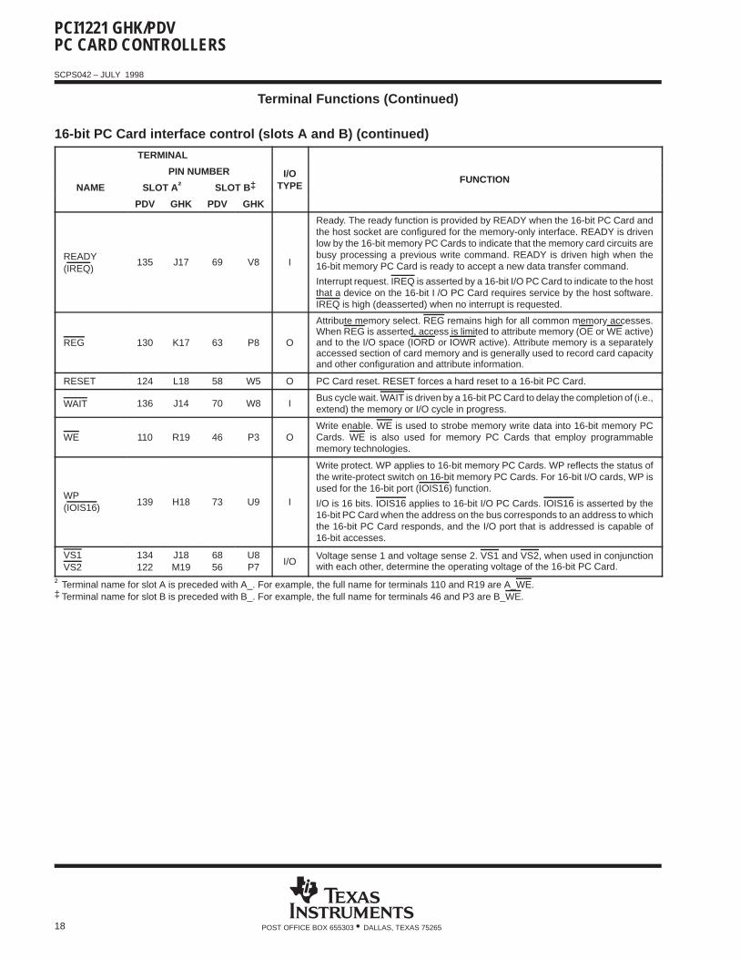
16-bit PC Card interface control (slots A and B) (continued)
TERMINAL
PIN NUMBER I/OFUNCTION
NAME SLOT A† SLOT B‡ TYPEFUNCTION
PDV GHK PDV GHK
READY(IREQ)
135 J17 69 V8 I
Ready. The ready function is provided by READY when the 16-bit PC Card andthe host socket are configured for the memory-only interface. READY is drivenlow by the 16-bit memory PC Cards to indicate that the memory card circuits arebusy processing a previous write command. READY is driven high when the16-bit memory PC Card is ready to accept a new data transfer command.
Interrupt request. IREQ is asserted by a 16-bit I/O PC Card to indicate to the hostthat a device on the 16-bit I /O PC Card requires service by the host software.IREQ is high (deasserted) when no interrupt is requested.
REG 130 K17 63 P8 O
Attribute memory select. REG remains high for all common memory accesses.When REG is asserted, access is limited to attribute memory (OE or WE active)and to the I/O space (IORD or IOWR active). Attribute memory is a separatelyaccessed section of card memory and is generally used to record card capacityand other configuration and attribute information.
RESET 124 L18 58 W5 O PC Card reset. RESET forces a hard reset to a 16-bit PC Card.
WAIT 136 J14 70 W8 IBus cycle wait. WAIT is driven by a 16-bit PC Card to delay the completion of (i.e.,extend) the memory or I/O cycle in progress.
WE 110 R19 46 P3 OWrite enable. WE is used to strobe memory write data into 16-bit memory PCCards. WE is also used for memory PC Cards that employ programmablememory technologies.
WP(IOIS16)
139 H18 73 U9 I
Write protect. WP applies to 16-bit memory PC Cards. WP reflects the status ofthe write-protect switch on 16-bit memory PC Cards. For 16-bit I/O cards, WP isused for the 16-bit port (IOIS16) function.
I/O is 16 bits. IOIS16 applies to 16-bit I/O PC Cards. IOIS16 is asserted by the16-bit PC Card when the address on the bus corresponds to an address to whichthe 16-bit PC Card responds, and the I/O port that is addressed is capable of16-bit accesses.
VS1VS2
134122
J18M19
6856
U8P7
I/OVoltage sense 1 and voltage sense 2. VS1 and VS2, when used in conjunctionwith each other, determine the operating voltage of the 16-bit PC Card.
† Terminal name for slot A is preceded with A_. For example, the full name for terminals 110 and R19 are A_WE.‡ Terminal name for slot B is preceded with B_. For example, the full name for terminals 46 and P3 are B_WE.
PCI1221 GHK/PDVPC CARD CONTROLLERS
SCPS042 – JULY 1998
19POST OFFICE BOX 655303 • DALLAS, TEXAS 75265
Terminal Functions (Continued)
CardBus PC Card interface system (slots A and B)
TERMINAL
PIN NUMBER I/OFUNCTION
NAME SLOT A† SLOT B‡ TYPEFUNCTION
PDV GHK PDV GHK
CCLK 112 P18 48 P6 O
CardBus PC Card clock. CCLK provides synchronous timing for all transactions onthe CardBus interface. All signals except CRST, CCLKRUN, CINT, CSTSCHG,CAUDIO, CCD2-1, and CVS2-CVS1 are sampled on the rising edge of CCLK, andall timing parameters are defined with the rising edge of this signal. CCLK operatesat the PCI bus clock frequency, but it can be stopped in the low state or slowed downfor power savings.
CCLKRUN 139 H18 73 U9 OCardBus PC Card clock run. CCLKRUN is used by a CardBus PC Card to requestan increase in the CCLK frequency, and by the PCI1221 to indicate that the CCLKfrequency is going to be decreased.
CRST 124 L18 58 W5 I/O
CardBus PC Card reset. CRST is used to bring CardBus PC Card-specificregisters, sequencers, and signals to a known state. When CRST is asserted, allCardBus PC Card signals must be 3-stated, and the PCI1221 drives these signalsto a valid logic level. Assertion can be asynchronous to CCLK, but deassertion mustbe synchronous to CCLK.
† Terminal name for slot A is preceded with A_. For example, the full name for terminals 112 and P18 are A_CCLK.‡ Terminal name for slot B is preceded with B_. For example, the full name for terminals 48 and P6 are B_CCLK.
PCI1221 GHK/PDVPC CARD CONTROLLERS
SCPS042 – JULY 1998
20 POST OFFICE BOX 655303 • DALLAS, TEXAS 75265
Terminal Functions (Continued)
CardBus PC Card address and data (slots A and B)
TERMINAL
PIN NUMBER I/OFUNCTION
NAME SLOT A† SLOT B‡ TYPEFUNCTION
PDV GHK PDV GHK
CAD31CAD30CAD29CAD28CAD27CAD26CAD25CAD24CAD23CAD22CAD21CAD20CAD19CAD18CAD17CAD16CAD15CAD14CAD13CAD12CAD11CAD10CAD9CAD8CAD7CAD6CAD5CAD4CAD3CAD2CAD1CAD0
14714514414214113313213112812612512312111911810310110299100989795939289908788848583
F19G17G18H15H14J19K14K15K19L15L17L19M18M15N19U15V15R14W15P14U14R13W14U13V13P12R12V12U12P11R11U11
8179787776676665626059575554533735363334323029272623242021181917
W11R10U10V10W10R8W7V7W6V6U6V5R6U5W4M6M2M3L5M1L6L2L1K5K3J6K1J2J3H1J1H2
I/O
PC Card address and data. These signals make up the multiplexed CardBus addressand data bus on the CardBus interface. During the address phase of a CardBus cycle,CAD31–CAD0 contain a 32-bit address. During the data phase of a CardBus cycle,CAD31–CAD0 contain data. CAD31 is the most-significant bit.
CC/BE3CC/BE2CC/BE1CC/BE0
13011710494
K17N18W16P13
63523928
P8T1N1K6
I/O
CardBus bus commands and byte enables. CC/BE3–CC/BE0 are multiplexed on thesame CardBus terminals. During the address phase of a CardBus cycle,CC/BE3–CC/BE0 defines the bus command. During the data phase, this 4-bit bus isused as byte enables. The byte enables determine which byte paths of the full 32-bitdata bus carry meaningful data. CC/BE0 applies to byte 0 (CAD7-CAD0), CC/BE1applies to byte 1 (CAD15-CAD8), CC/BE2 applies to byte 2 (CAD23-CAD8), andCC/BE3 applies to byte 3 (CAD31-CAD24).
CPAR 106 R17 41 N3 I/O
CardBus parity. In all CardBus read and write cycles, the PCI1221 calculates evenparity across the CAD and CC/BE buses. As an initiator during CardBus cycles, thePCI1221 outputs CPAR with a one-CCLK delay. As a target during CardBus cycles,the calculated parity is compared to the initiator’s parity indicator; a compare errorresults in a parity error assertion.
† Terminal name for slot A is preceded with A_. For example, the full name for terminals 106 and R17 are A_CPAR.‡ Terminal name for slot B is preceded with B_. For example, the full name for terminals 41 and N3 are B_CPAR.
PCI1221 GHK/PDVPC CARD CONTROLLERS
SCPS042 – JULY 1998
21POST OFFICE BOX 655303 • DALLAS, TEXAS 75265
Terminal Functions (Continued)
CardBus PC Card interface control (slots A and B)
TERMINAL
PIN NUMBER I/OFUNCTION
NAME SLOT A† SLOT B‡ TYPEFUNCTION
PDV GHK PDV GHK
CAUDIO 137 J15 71 W9 ICardBus audio. CAUDIO is a digital input signal from a PC Card to the systemspeaker. The PCI1221 supports the binary audio mode and outputs a binary signalfrom the card to SPKROUT.
CBLOCK 107 P15 42 N6 I/O CardBus lock. CBLOCK is used to gain exclusive access to a target.
CCD1 82 V11 16 H3I
CardBus detect 1 and CardBus detect 2. CCD1 and CCD2 are used in conjunctionwith CVS1 and CVS2 to identify card insertion and interrogate cards to determine
CCD2 140 H17 74 R9I with CVS1 and CVS2 to identify card insertion and interrogate cards to determine
the operating voltage and card type.
CDEVSEL 111 P17 47 R1 I/O
CardBus device select. The PCI1221 asserts CDEVSEL to claim a CardBus cycleas the target device. As a CardBus initiator on the bus, the PCI1221 monitorsCDEVSEL until a target responds. If no target responds before timeout occurs, thePCI1221 terminates the cycle with an initiator abort.
CFRAME 116 N17 51 R3 I/O
CardBus cycle frame. CFRAME is driven by the initiator of a CardBus bus cycle.CFRAME is asserted to indicate that a bus transaction is beginning, and datatransfers continue while this signal is asserted. When CFRAME is deasserted, theCardBus bus transaction is in the final data phase.
CGNT 110 R19 46 P3 ICardBus bus grant. CGNT is driven by the PCI1221 to grant a CardBus PC Cardaccess to the CardBus bus after the current data transaction has been completed.
CINT 135 J17 69 V8 ICardBus interrupt. CINT is asserted low by a CardBus PC Card to request interruptservicing from the host.
CIRDY 115 M14 50 P5 I/O
CardBus initiator ready. CIRDY indicates the CardBus initiator’s ability to completethe current data phase of the transaction. A data phase is completed on a risingedge of CCLK when both CIRDY and CTRDY are asserted. Until CIRDY andCTRDY are both sampled asserted, wait states are inserted.
CPERR 108 N14 43 P1 I/OCardBus parity error. CPERR is used to report parity errors during CardBustransactions, except during special cycles. It is driven low by a target two clocksfollowing that data when a parity error is detected.
CREQ 127 L14 61 R7 ICardBus request. CREQ indicates to the arbiter that the CardBus PC Card desiresuse of the CardBus bus as an initiator.
CSERR 136 J14 70 W8 I
CardBus system error. CSERR reports address parity errors and other systemerrors that could lead to catastrophic results. CSERR is driven by the cardsynchronous to CCLK, but deasserted by a weak pullup, and may take severalCCLK periods. The PCI1221 can report CSERR to the system by assertion of SERRon the PCI interface.
CSTOP 109 R18 45 N5 I/OCardBus stop. CSTOP is driven by a CardBus target to request the initiator to stopthe current CardBus transaction. CSTOP is used for target disconnects, and iscommonly asserted by target devices that do not support burst data transfers.
CSTSCHG 138 H19 72 V9 ICardBus status change. CSTSCHG is used to alert the system to a change in thecard’s status, and is used as a wake-up mechanism.
CTRDY 114 P19 49 R2 I/O
CardBus target ready. CTRDY indicates the CardBus target’s ability to complete thecurrent data phase of the transaction. A data phase is completed on a rising edgeof CCLK, when both CIRDY and CTRDY are asserted; until this time, wait statesare inserted.
CVS1 134 J18 68 U8I/O
CardBus voltage sense 1 and CardBus voltage sense 2. CVS1 and CVS2 are usedin conjunction with CCD1 and CCD2 to identify card insertion and interrogate cardsCVS2 122 M19 56 P7 I/O in conjunction with CCD1 and CCD2 to identify card insertion and interrogate cardsto determine the operating voltage and card type.
† Terminal name for slot A is preceded with A_. For example, the full name for terminals 137 and J15 are A_CAUDIO.‡ Terminal name for slot B is preceded with B_. For example, the full name for terminals 71 and W9 are B_CAUDIO.
PCI1221 GHK/PDVPC CARD CONTROLLERS
SCPS042 – JULY 1998
22 POST OFFICE BOX 655303 • DALLAS, TEXAS 75265
power supply sequencingThe PCI1221 contains 3.3-V I/O buffers with 5-V tolerance requiring a core power supply and clamping voltage.The core power supply is always 3.3 V. The clamp voltage can be either 3.3 V or 5 V, depending on the interface.The following power-up and power-down sequences are recommended.
The power-up sequence is:
1. Apply 3.3-V power to the core.
2. Assert PRST to the device to disable the outputs during power up. Output drivers must be powered up inthe high-impedance state to prevent high current levels through the clamp diodes to the 5-V supply.
3. Apply the clamping voltage.
The power-down sequence is:
1. Use PRST to switch outputs to a high-impedance state.
2. Remove the clamping voltage.
3. Remove the 3.3-V power from the core.
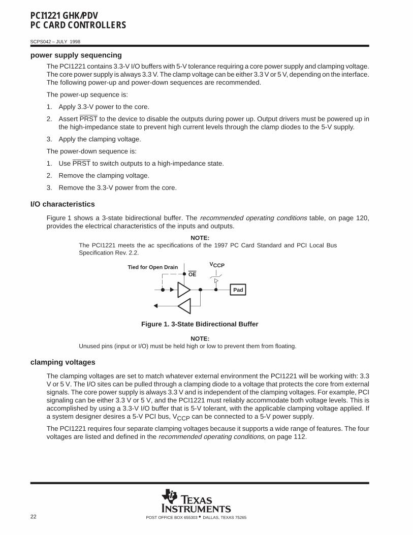
I/O characteristics
Figure 1 shows a 3-state bidirectional buffer. The recommended operating conditions table, on page 120,provides the electrical characteristics of the inputs and outputs.
NOTE:The PCI1221 meets the ac specifications of the 1997 PC Card Standard and PCI Local BusSpecification Rev. 2.2.
Tied for Open DrainOE
Pad
VCCP
Figure 1. 3-State Bidirectional Buffer
NOTE:Unused pins (input or I/O) must be held high or low to prevent them from floating.
clamping voltages
The clamping voltages are set to match whatever external environment the PCI1221 will be working with: 3.3V or 5 V. The I/O sites can be pulled through a clamping diode to a voltage that protects the core from externalsignals. The core power supply is always 3.3 V and is independent of the clamping voltages. For example, PCIsignaling can be either 3.3 V or 5 V, and the PCI1221 must reliably accommodate both voltage levels. This isaccomplished by using a 3.3-V I/O buffer that is 5-V tolerant, with the applicable clamping voltage applied. Ifa system designer desires a 5-V PCI bus, VCCP can be connected to a 5-V power supply.
The PCI1221 requires four separate clamping voltages because it supports a wide range of features. The fourvoltages are listed and defined in the recommended operating conditions, on page 112.
PCI1221 GHK/PDVPC CARD CONTROLLERS
SCPS042 – JULY 1998
23POST OFFICE BOX 655303 • DALLAS, TEXAS 75265
peripheral component interconnect (PCI) interface
The PCI1221 is fully compliant with the PCI Local Bus Specification Rev. 2.2. The PCI1221 provides all requiredsignals for PCI master or slave operation, and may operate in either a 5-V of 3.3-V signaling environment byconnecting the VCCP terminals to the desired voltage level. In addition to the mandatory PCI signals, thePCI1221 provides the optional interrupt signals INTA and INTB.
PCI bus lock (LOCK)
The bus-locking protocol defined in the PCI specification is not highly recommended, but is provided on thePCI1221 as an additional compatibility feature. The PCI LOCK signal can be routed to the MFUNC4 terminalvia the multifunction routing register, see the multifunction routing register description on page 62 for details.Note that the use of LOCK is only supported by PCI-to-CardBus bridges in the downstream direction (away fromthe processor).
PCI LOCK indicates an atomic operation that may require multiple transactions to complete. When LOCK isasserted, nonexclusive transactions can proceed to an address that is not currently locked. A grant to start atransaction on the PCI bus does not guarantee control of LOCK; control of LOCK is obtained under its ownprotocol. It is possible for different initiators to use the PCI bus while a single master retains ownership of LOCK.Note that the CardBus signal for this protocol is CBLOCK to avoid confusion with the bus clock.
An agent may need to do an exclusive operation because a critical access to memory might be broken intoseveral transactions, but the master wants exclusive rights to a region of memory. The granularity of the lockis defined by PCI to be 16 bytes, aligned. The lock protocol defined by PCI allows a resource lock withoutinterfering with nonexclusive real-time data transfer, such as video.
The PCI bus arbiter may be designed to support only complete bus locks using the LOCK protocol. In thisscenario, the arbiter will not grant the bus to any other agent (other than the LOCK master) while LOCK isasserted. A complete bus lock may have a significant impact on the performance of the video. The arbiter thatsupports complete bus lock must grant the bus to the cache to perform a writeback due to a snoop to a modifiedline when a locked operation is in progress.
The PCI1221 supports all LOCK protocol associated with PCI-to-PCI bridges, as also defined forPCI-to-CardBus bridges. This includes disabling write posting while a locked operation is in progress, which cansolve a potential deadlock when using devices such as PCI-to-PCI bridges. The potential deadlock can occurif a CardBus target supports delayed transactions and blocks access to the target until it completes a delayedread. This target characteristic is prohibited by the 2.2 PCI specification, and the issue is resolved by the PCImaster using LOCK.
loading subsystem identification
The subsystem vendor ID register and subsystem ID register make up a doubleword of PCI configuration spacelocated at offset 40h for functions 0 and 1. This doubleword register is used for system and option card (mobiledock) identification purposes and is required by some operating systems. Implementation of this uniqueidentifier register is a PC 95 requirement.
The PCI1221 offers two mechanisms to load a read-only value into the subsystem registers. The firstmechanism relies upon the system BIOS providing the subsystem ID value. The default access mode to thesubsystem registers is read only, but can be made read/write by setting the SUBSYSRW bit in the system controlregister (bit 5, at PCI offset 80h). Once this bit is set, the BIOS can write a subsystem identification value intothe registers at offset 40h. The BIOS must clear the SUBSYSRW bit such that the subsystem vendor ID registerand subsystem ID register is limited to read-only access. This approach saves the added cost of implementingthe serial electrically erasable programmable ROM (EEPROM).
PCI1221 GHK/PDVPC CARD CONTROLLERS
SCPS042 – JULY 1998
24 POST OFFICE BOX 655303 • DALLAS, TEXAS 75265
loading subsystem identification (continued)
In some conditions, such as in a docking environment, the subsystem vendor ID register and subsystem IDregister must be loaded with a unique identifier via a serial EEPROM. The PCI1221 loads the data from the serialEEPROM after a reset of the primary bus. Note that the SUSPEND input gates the PCI reset from the entirePCI1221 core, including the serial bus state machine (see suspend mode, on page 40, for details on usingSUSPEND).
The PCI1221 provides a two-line serial bus host controller that can be used to interface to a serial EEPROM.Refer to serial bus interface on page 29 for details on the two-wire serial bus controller and applications.
PC Card applications
This section describes the PC Card interfaces of the PCI1221:
Card insertion/removal and recognition P2C power-switch interface Zoom video support Speaker and audio applications LED socket activity indicators CardBus socket registers
PC Card insertion/removal and recognition
The 1997 PC Card Standard addresses the card-detection and recognition process through an interrogationprocedure that the socket must initiate on card insertion into a cold, nonpowered socket. Through thisinterrogation, card voltage requirements and interface (16 bit versus CardBus) are determined.
The scheme uses the CD1, CD2, VS1, and VS2 signals (CCD1, CCD2, CVS1, and CVS2 for CardBus). Theconfiguration of these four terminals identifies the card type and voltage requirements of the PC Card interface.The encoding scheme is defined in the 1997 PC Card Standard and in Table 5.
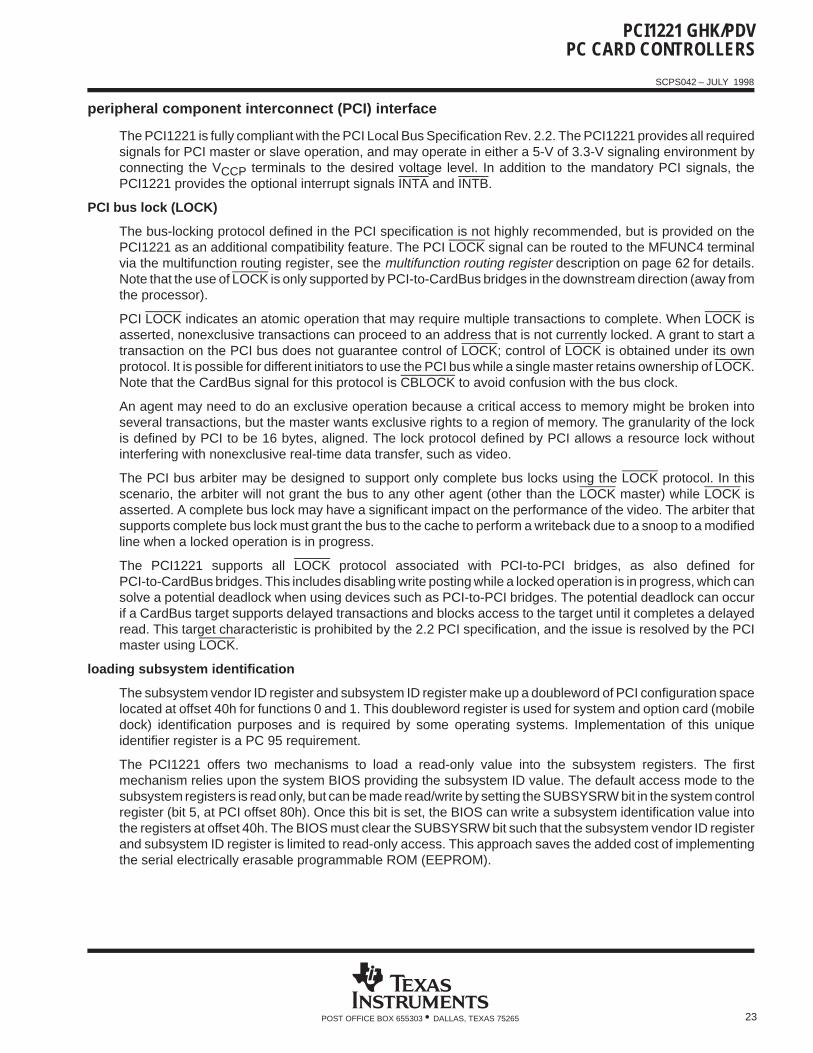
Table 5. PC Card Card-Detect and Voltage-Sense Connections
CD2//CCD2 CD1//CCD1 VS2//CVS2 VS1//CVS1 KEY INTERFACE VOLTAGE
Ground Ground Open Open 5 V 16-bit PC Card 5 V
Ground Ground Open Ground 5 V 16-bit PC Card 5 V and 3.3 V
Ground Ground Ground Ground 5 V 16-bit PC Card 5 V, 3.3 V, and X.X V
Ground Ground Open Ground LV 16-bit PC Card 3.3 V
Ground Connect to CVS1 Open Connect to CCD1 LV CardBus PC Card 3.3 V
Ground Ground Ground Ground LV 16-bit PC Card 3.3 V and X.X V
Connect to CVS2 Ground Connect to CCD2 Ground LV CardBus PC Card 3.3 V and X.X V
Connect to CVS1 Ground Ground Connect to CCD2 LV CardBus PC Card 3.3 V, X.X V, and Y.Y V
Ground Ground Ground Open LV 16-bit PC Card Y.Y V
Connect to CVS2 Ground Connect to CCD2 Open LV CardBus PC Card Y.Y V
Ground Connect to CVS2 Connect to CCD1 Open LV CardBus PC Card X.X V and Y.Y V
Connect to CVS1 Ground Open Connect to CCD2 LV CardBus PC Card Y.Y V
Ground Connect to CVS1 Ground Connect to CCD1 Reserved
Ground Connect to CVS2 Connect to CCD1 Ground Reserved
PCI1221 GHK/PDVPC CARD CONTROLLERS
SCPS042 – JULY 1998
25POST OFFICE BOX 655303 • DALLAS, TEXAS 75265
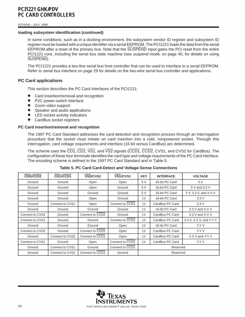
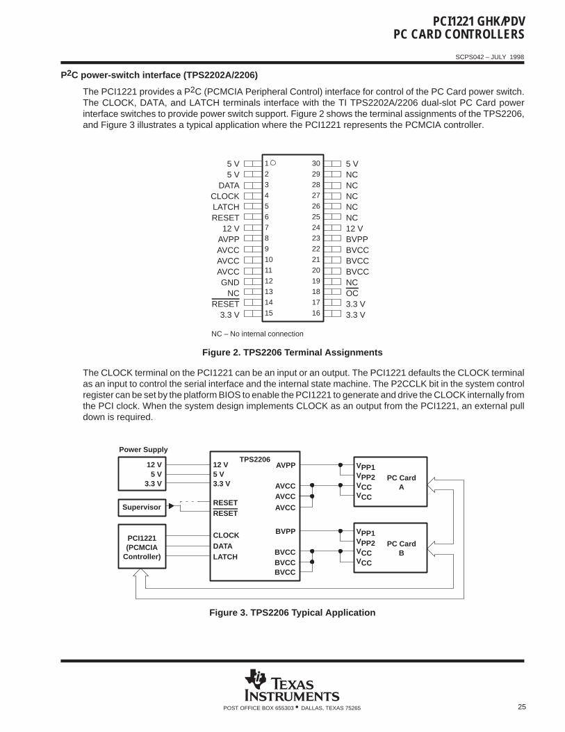
P2C power-switch interface (TPS2202A/2206)
The PCI1221 provides a P2C (PCMCIA Peripheral Control) interface for control of the PC Card power switch.The CLOCK, DATA, and LATCH terminals interface with the TI TPS2202A/2206 dual-slot PC Card powerinterface switches to provide power switch support. Figure 2 shows the terminal assignments of the TPS2206,and Figure 3 illustrates a typical application where the PCI1221 represents the PCMCIA controller.
1
2
3
4
5
6
78
9
10
11
12
13
14
15
30
29
28
27
26
25
2423
22
21
20
19
18
17
16
5 V5 V
DATACLOCKLATCHRESET
12 VAVPPAVCCAVCCAVCCGND
NCRESET
3.3 V
5 VNCNCNCNCNC12 VBVPPBVCCBVCCBVCCNCOC3.3 V3.3 V
NC – No internal connection
Figure 2. TPS2206 Terminal Assignments
The CLOCK terminal on the PCI1221 can be an input or an output. The PCI1221 defaults the CLOCK terminalas an input to control the serial interface and the internal state machine. The P2CCLK bit in the system controlregister can be set by the platform BIOS to enable the PCI1221 to generate and drive the CLOCK internally fromthe PCI clock. When the system design implements CLOCK as an output from the PCI1221, an external pulldown is required.
PCI1221(PCMCIA
Controller)
12 V
Power Supply
VPP1VPP2VCCVCC
PC CardA
TPS2206
5 V3.3 V
CLOCK VPP1VPP2VCCVCC
PC CardB
12 V5 V3.3 V
AVPP
AVCCAVCC
BVPP
BVCCBVCCBVCC
AVCCSupervisorRESETRESET
DATALATCH
Figure 3. TPS2206 Typical Application
PCI1221 GHK/PDVPC CARD CONTROLLERS
SCPS042 – JULY 1998
26 POST OFFICE BOX 655303 • DALLAS, TEXAS 75265
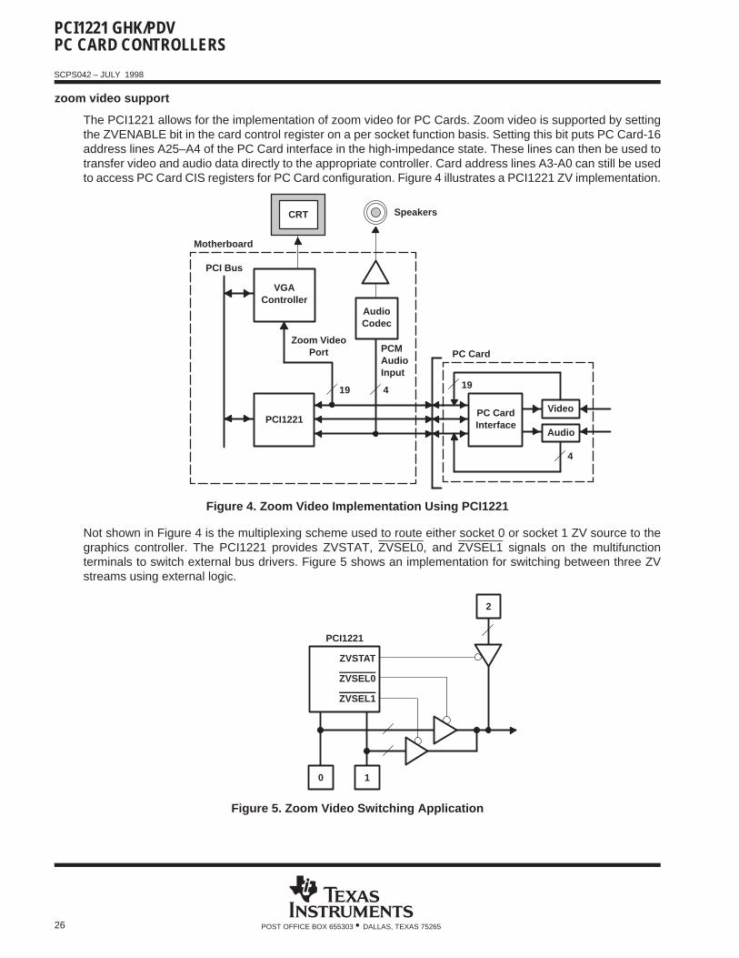
zoom video support
The PCI1221 allows for the implementation of zoom video for PC Cards. Zoom video is supported by settingthe ZVENABLE bit in the card control register on a per socket function basis. Setting this bit puts PC Card-16address lines A25–A4 of the PC Card interface in the high-impedance state. These lines can then be used totransfer video and audio data directly to the appropriate controller. Card address lines A3-A0 can still be usedto access PC Card CIS registers for PC Card configuration. Figure 4 illustrates a PCI1221 ZV implementation.
CRT
VGAController
AudioCodec
PCI1221
19 4
Zoom VideoPort PCM
AudioInput
PCI Bus
PC CardInterface
Video
Audio
19
4
PC Card
Motherboard
Speakers
Figure 4. Zoom Video Implementation Using PCI1221
Not shown in Figure 4 is the multiplexing scheme used to route either socket 0 or socket 1 ZV source to thegraphics controller. The PCI1221 provides ZVSTAT, ZVSEL0, and ZVSEL1 signals on the multifunctionterminals to switch external bus drivers. Figure 5 shows an implementation for switching between three ZVstreams using external logic.
ZVSTAT
ZVSEL0
ZVSEL1
PCI1221
2
0 1
Figure 5. Zoom Video Switching Application
PCI1221 GHK/PDVPC CARD CONTROLLERS
SCPS042 – JULY 1998
27POST OFFICE BOX 655303 • DALLAS, TEXAS 75265
zoom video support (continued)
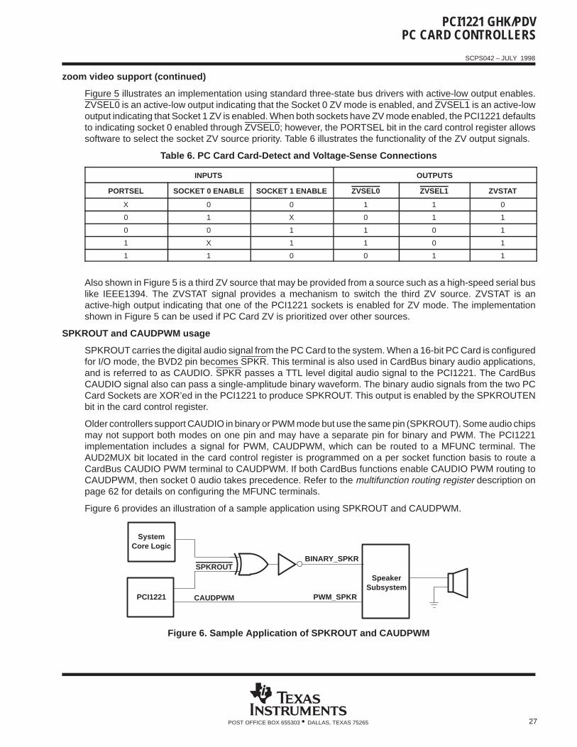
Figure 5 illustrates an implementation using standard three-state bus drivers with active-low output enables.ZVSEL0 is an active-low output indicating that the Socket 0 ZV mode is enabled, and ZVSEL1 is an active-lowoutput indicating that Socket 1 ZV is enabled. When both sockets have ZV mode enabled, the PCI1221 defaultsto indicating socket 0 enabled through ZVSEL0; however, the PORTSEL bit in the card control register allowssoftware to select the socket ZV source priority. Table 6 illustrates the functionality of the ZV output signals.
Table 6. PC Card Card-Detect and Voltage-Sense Connections
INPUTS OUTPUTS
PORTSEL SOCKET 0 ENABLE SOCKET 1 ENABLE ZVSEL0 ZVSEL1 ZVSTAT
X 0 0 1 1 0
0 1 X 0 1 1
0 0 1 1 0 1
1 X 1 1 0 1
1 1 0 0 1 1
Also shown in Figure 5 is a third ZV source that may be provided from a source such as a high-speed serial buslike IEEE1394. The ZVSTAT signal provides a mechanism to switch the third ZV source. ZVSTAT is anactive-high output indicating that one of the PCI1221 sockets is enabled for ZV mode. The implementationshown in Figure 5 can be used if PC Card ZV is prioritized over other sources.
SPKROUT and CAUDPWM usage
SPKROUT carries the digital audio signal from the PC Card to the system. When a 16-bit PC Card is configuredfor I/O mode, the BVD2 pin becomes SPKR. This terminal is also used in CardBus binary audio applications,and is referred to as CAUDIO. SPKR passes a TTL level digital audio signal to the PCI1221. The CardBusCAUDIO signal also can pass a single-amplitude binary waveform. The binary audio signals from the two PCCard Sockets are XOR’ed in the PCI1221 to produce SPKROUT. This output is enabled by the SPKROUTENbit in the card control register.
Older controllers support CAUDIO in binary or PWM mode but use the same pin (SPKROUT). Some audio chipsmay not support both modes on one pin and may have a separate pin for binary and PWM. The PCI1221implementation includes a signal for PWM, CAUDPWM, which can be routed to a MFUNC terminal. TheAUD2MUX bit located in the card control register is programmed on a per socket function basis to route aCardBus CAUDIO PWM terminal to CAUDPWM. If both CardBus functions enable CAUDIO PWM routing toCAUDPWM, then socket 0 audio takes precedence. Refer to the multifunction routing register description onpage 62 for details on configuring the MFUNC terminals.
Figure 6 provides an illustration of a sample application using SPKROUT and CAUDPWM.
SpeakerSubsystem
BINARY_SPKR
SystemCore Logic
PCI1221 CAUDPWM
SPKROUT
PWM_SPKR
Figure 6. Sample Application of SPKROUT and CAUDPWM
PCI1221 GHK/PDVPC CARD CONTROLLERS
SCPS042 – JULY 1998
28 POST OFFICE BOX 655303 • DALLAS, TEXAS 75265
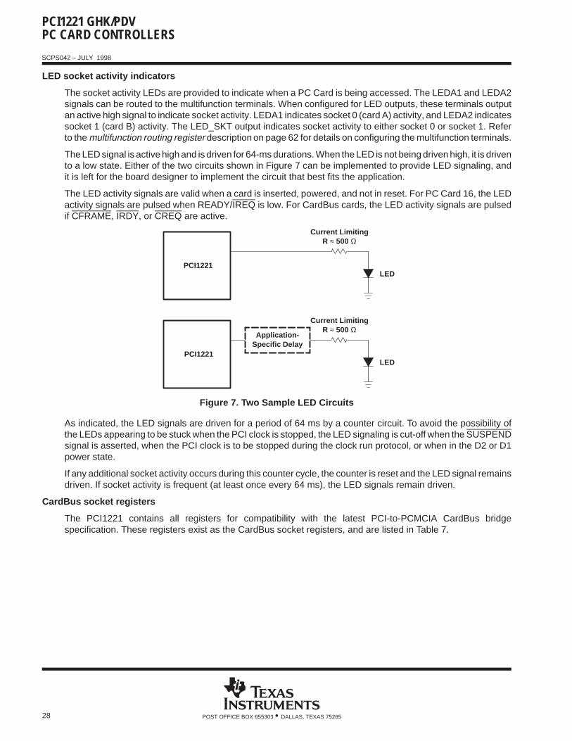
LED socket activity indicators
The socket activity LEDs are provided to indicate when a PC Card is being accessed. The LEDA1 and LEDA2signals can be routed to the multifunction terminals. When configured for LED outputs, these terminals outputan active high signal to indicate socket activity. LEDA1 indicates socket 0 (card A) activity, and LEDA2 indicatessocket 1 (card B) activity. The LED_SKT output indicates socket activity to either socket 0 or socket 1. Referto the multifunction routing register description on page 62 for details on configuring the multifunction terminals.
The LED signal is active high and is driven for 64-ms durations. When the LED is not being driven high, it is drivento a low state. Either of the two circuits shown in Figure 7 can be implemented to provide LED signaling, andit is left for the board designer to implement the circuit that best fits the application.
The LED activity signals are valid when a card is inserted, powered, and not in reset. For PC Card 16, the LEDactivity signals are pulsed when READY/IREQ is low. For CardBus cards, the LED activity signals are pulsedif CFRAME, IRDY, or CREQ are active.
PCI1221
Application-Specific Delay
Current LimitingR ≈ 500 Ω
LED
PCI1221
Current LimitingR ≈ 500 Ω
LED
Figure 7. Two Sample LED Circuits
As indicated, the LED signals are driven for a period of 64 ms by a counter circuit. To avoid the possibility ofthe LEDs appearing to be stuck when the PCI clock is stopped, the LED signaling is cut-off when the SUSPENDsignal is asserted, when the PCI clock is to be stopped during the clock run protocol, or when in the D2 or D1power state.
If any additional socket activity occurs during this counter cycle, the counter is reset and the LED signal remainsdriven. If socket activity is frequent (at least once every 64 ms), the LED signals remain driven.
CardBus socket registers
The PCI1221 contains all registers for compatibility with the latest PCI-to-PCMCIA CardBus bridgespecification. These registers exist as the CardBus socket registers, and are listed in Table 7.
PCI1221 GHK/PDVPC CARD CONTROLLERS
SCPS042 – JULY 1998
29POST OFFICE BOX 655303 • DALLAS, TEXAS 75265
Table 7. CardBus Socket Registers
REGISTER NAME OFFSET
Socket event 00h
Socket mask 04h
Socket present state 08h
Socket force event 0Ch
Socket control 10h
Reserved 14h
Reserved 18h
Reserved 1Ch
Socket power management 20h
serial bus interface
The PCI1221 provides a serial bus interface to load subsystem identification and select register defaults througha serial EEPROM and to provide a PC Card power switch interface alternative to P2C. Refer to P2Cpower-switch interface (TPS2202A/2206) on page 25 for details. The PCI1221 serial bus interface is compatiblewith various I2C and SMBus components.
serial bus interface implementation
The PCI1221 defaults to serial bus interface are disabled. To enable the serial interface, a pulldown resistormust be implemented on the LATCH terminal and the appropriate pullup must be implemented on the SDA andSCL signals, i.e. the MFUNC1 and MFUNC4 terminals. When the interface is detected, the SBDETECT bit inthe system control register is set. The SBDETECT bit is cleared by a write back of 1.
The PCI1221 implements a two pin serial interface with one clock signal (SCL) and one data signal (SDA). Whena pulldown is provided on the LATCH terminal, the SCL signal is mapped to the MFUNC4 terminal and the SDAsignal is mapped to the MFUNC1 terminal. The PCI1221 drives SCL at nearly 100 kHz during data transfers,which is the maximum specified frequency for standard mode I2C. An example application implementing thetwo-wire serial bus is illustrated in Figure 8.
SerialEEPROM
A0
A1
A2
PCI1221
MFUNC4
MFUNC1
LATCH
SCL
SDA
VCC
Figure 8. Serial EEPROM Application
Some serial device applications may include PC Card power switches, ZV source switches, card ejectors, orother devices that may enhance the user’s PC Card experience. The serial EEPROM device and PC Card powerswitches are discussed in the sections that follow.
serial bus interface protocol
The SCL and SDA signals are bidirectional, open-drain signals and require pullup resistors as shown in FigureFigure 8. The PCI1221 supports up to 100 Kb/s data transfer rate and is compatible with standard mode I2Cusing seven-bit addressing.
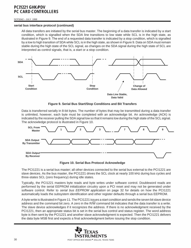
PCI1221 GHK/PDVPC CARD CONTROLLERS
SCPS042 – JULY 1998
30 POST OFFICE BOX 655303 • DALLAS, TEXAS 75265
serial bus interface protocol (continued)
All data transfers are initiated by the serial bus master. The beginning of a data transfer is indicated by a startcondition, which is signalled when the SDA line transitions to low state while SCL is in the high state, asillustrated in Figure 9. The end of a requested data transfer is indicated by a stop condition, which is signalledby a low to high transition of SDA while SCL is in the high state, as shown in Figure 9. Data on SDA must remainstable during the high state of the SCL signal, as changes on the SDA signal during the high state of SCL areinterpreted as control signals, that is, a start or a stop condition.
SDA
SCL
StartCondition
StopCondition
Change ofData Allowed
Data Line Stable,Data Valid
Figure 9. Serial Bus Start/Stop Conditions and Bit Transfers
Data is transferred serially in 8-bit bytes. The number of bytes that may be transmitted during a data transferis unlimited, however, each byte must be completed with an acknowledge bit. An acknowledge (ACK) isindicated by the receiver pulling the SDA signal low so that it remains low during the high state of the SCL signal.The acknowledge protocol is illustrated in Figure 10.
SCL FromMaster 1 2 3 7 8 9
SDA Output By Transmitter
SDA OutputBy Receiver
Figure 10. Serial Bus Protocol Acknowledge
The PCI1221 is a serial bus master; all other devices connected to the serial bus external to the PCI1221 areslave devices. As the bus master, the PCI1221 drives the SCL clock at nearly 100 kHz during bus cycles andthree-states SCL (zero frequency) during idle states.
Typically, the PCI1221 masters byte reads and byte writes under software control. Doubleword reads areperformed by the serial EEPROM initialization circuitry upon a PCI reset and may not be generated undersoftware control. Refer to serial bus EEPROM application on page 32 for details on how the PCI1221automatically loads the subsystem identification and other register defaults through a serial bus EEPROM.
A byte write is illustrated in Figure 11. The PCI1221 issues a start condition and sends the seven bit slave deviceaddress and the command bit zero. A zero in the R/W command bit indicates that the data transfer is a write.The slave device acknowledges if it recognizes the address. If there is no acknowledgment received by thePCI1221, then an appropriate status bit is set in the serial bus control and status register. The word addressbyte is then sent by the PCI1221 and another slave acknowledgment is expected. Then the PCI1221 deliversthe data byte MSB first and expects a final acknowledgment before issuing the stop condition.
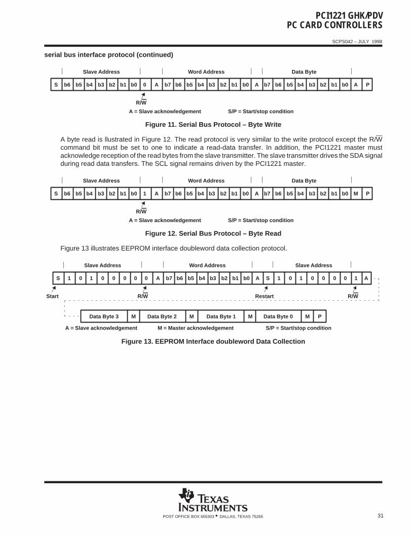
PCI1221 GHK/PDVPC CARD CONTROLLERS
SCPS042 – JULY 1998
31POST OFFICE BOX 655303 • DALLAS, TEXAS 75265
serial bus interface protocol (continued)
S b6 b4b5 b3 b2 b1 b0 0 b7 b6 b5 b4 b3 b2 b1 b0A A
Slave Address Word Address
R/W
S/P = Start/stop conditionA = Slave acknowledgement
b7 b6 b4b5 b3 b2 b1 b0 A P
Data Byte
Figure 11. Serial Bus Protocol – Byte Write
A byte read is llustrated in Figure 12. The read protocol is very similar to the write protocol except the R/Wcommand bit must be set to one to indicate a read-data transfer. In addition, the PCI1221 master mustacknowledge reception of the read bytes from the slave transmitter. The slave transmitter drives the SDA signalduring read data transfers. The SCL signal remains driven by the PCI1221 master.
S b6 b4b5 b3 b2 b1 b0 1 b7 b6 b5 b4 b3 b2 b1 b0A A
Slave Address Word Address
R/W
S/P = Start/stop conditionA = Slave acknowledgement
b7 b6 b4b5 b3 b2 b1 b0 M P
Data Byte
Figure 12. Serial Bus Protocol – Byte Read
Figure 13 illustrates EEPROM interface doubleword data collection protocol.
S 1 10 0 0 0 0 0 b7 b6 b5 b4 b3 b2 b1 b0A A
Slave Address Word Address
R/W
Data Byte 2 Data Byte 1 Data Byte 0 M PMM
M = Master acknowledgement S/P = Start/stop conditionA = Slave acknowledgement
Data Byte 3 M
S 1 10 0 0 0 0 1 A
Restart R/W
Slave Address
Start
Figure 13. EEPROM Interface doubleword Data Collection
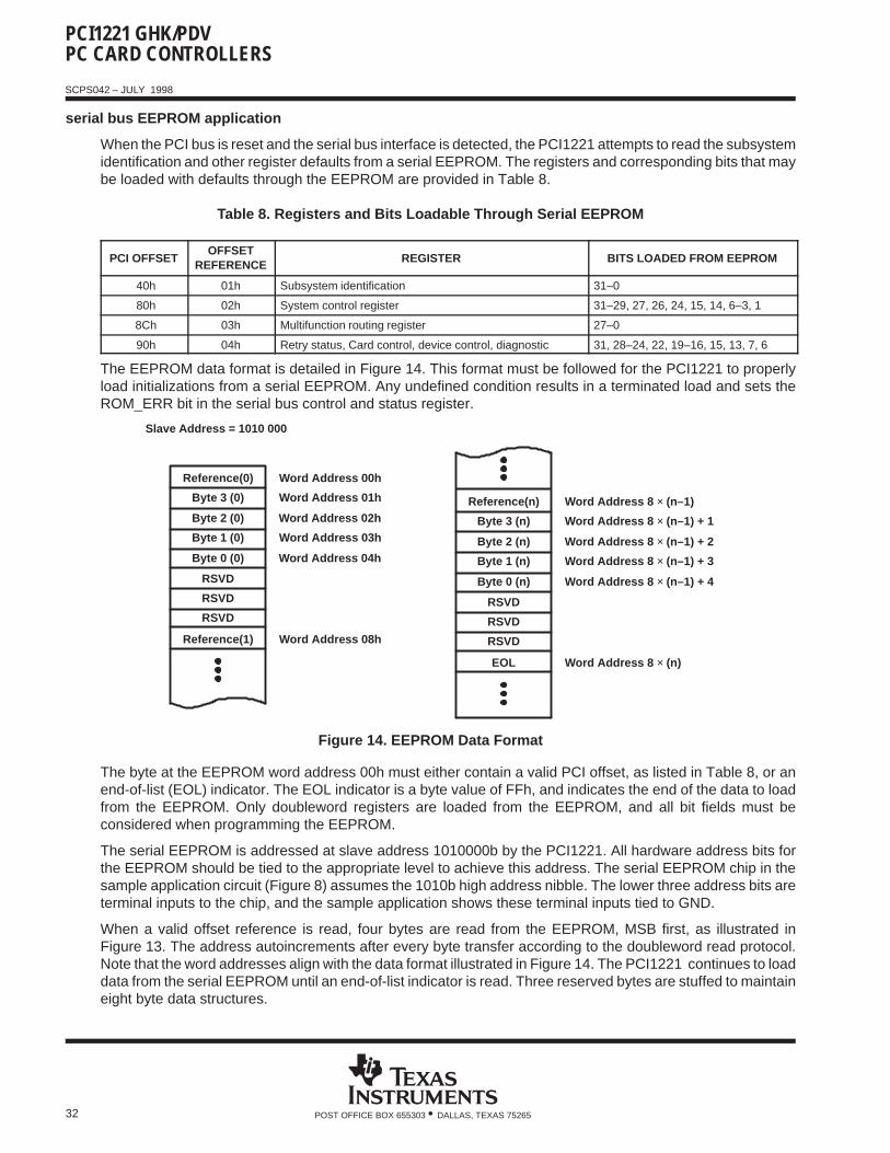
PCI1221 GHK/PDVPC CARD CONTROLLERS
SCPS042 – JULY 1998
32 POST OFFICE BOX 655303 • DALLAS, TEXAS 75265
serial bus EEPROM application
When the PCI bus is reset and the serial bus interface is detected, the PCI1221 attempts to read the subsystemidentification and other register defaults from a serial EEPROM. The registers and corresponding bits that maybe loaded with defaults through the EEPROM are provided in Table 8.
Table 8. Registers and Bits Loadable Through Serial EEPROM
PCI OFFSETOFFSET
REFERENCE REGISTER BITS LOADED FROM EEPROM
40h 01h Subsystem identification 31–0
80h 02h System control register 31–29, 27, 26, 24, 15, 14, 6–3, 1
8Ch 03h Multifunction routing register 27–0
90h 04h Retry status, Card control, device control, diagnostic 31, 28–24, 22, 19–16, 15, 13, 7, 6
The EEPROM data format is detailed in Figure 14. This format must be followed for the PCI1221 to properlyload initializations from a serial EEPROM. Any undefined condition results in a terminated load and sets theROM_ERR bit in the serial bus control and status register.
Slave Address = 1010 000
Reference(0) Word Address 00h
Byte 3 (0) Word Address 01h
Byte 2 (0) Word Address 02h
Byte 1 (0) Word Address 03h
Byte 0 (0) Word Address 04h
RSVD
RSVD
RSVD
Reference(1) Word Address 08h
Reference(n) Word Address 8 × (n–1)
Byte 3 (n) Word Address 8 × (n–1) + 1
Byte 2 (n) Word Address 8 × (n–1) + 2
Byte 1 (n) Word Address 8 × (n–1) + 3
Byte 0 (n) Word Address 8 × (n–1) + 4
RSVD
RSVD
RSVD
EOL Word Address 8 × (n)
Figure 14. EEPROM Data Format
The byte at the EEPROM word address 00h must either contain a valid PCI offset, as listed in Table 8, or anend-of-list (EOL) indicator. The EOL indicator is a byte value of FFh, and indicates the end of the data to loadfrom the EEPROM. Only doubleword registers are loaded from the EEPROM, and all bit fields must beconsidered when programming the EEPROM.
The serial EEPROM is addressed at slave address 1010000b by the PCI1221. All hardware address bits forthe EEPROM should be tied to the appropriate level to achieve this address. The serial EEPROM chip in thesample application circuit (Figure 8) assumes the 1010b high address nibble. The lower three address bits areterminal inputs to the chip, and the sample application shows these terminal inputs tied to GND.
When a valid offset reference is read, four bytes are read from the EEPROM, MSB first, as illustrated inFigure 13. The address autoincrements after every byte transfer according to the doubleword read protocol.Note that the word addresses align with the data format illustrated in Figure 14. The PCI1221 continues to loaddata from the serial EEPROM until an end-of-list indicator is read. Three reserved bytes are stuffed to maintaineight byte data structures.
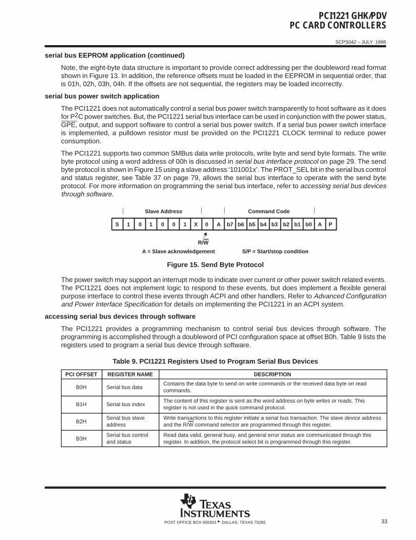
PCI1221 GHK/PDVPC CARD CONTROLLERS
SCPS042 – JULY 1998
33POST OFFICE BOX 655303 • DALLAS, TEXAS 75265
serial bus EEPROM application (continued)
Note, the eight-byte data structure is important to provide correct addressing per the doubleword read formatshown in Figure 13. In addition, the reference offsets must be loaded in the EEPROM in sequential order, thatis 01h, 02h, 03h, 04h. If the offsets are not sequential, the registers may be loaded incorrectly.
serial bus power switch application
The PCI1221 does not automatically control a serial bus power switch transparently to host software as it doesfor P2C power switches. But, the PCI1221 serial bus interface can be used in conjunction with the power status,GPE, output, and support software to control a serial bus power switch. If a serial bus power switch interfaceis implemented, a pulldown resistor must be provided on the PCI1221 CLOCK terminal to reduce powerconsumption.
The PCI1221 supports two common SMBus data write protocols, write byte and send byte formats. The writebyte protocol using a word address of 00h is discussed in serial bus interface protocol on page 29. The sendbyte protocol is shown in Figure 15 using a slave address ‘101001x’. The PROT_SEL bit in the serial bus controland status register, see Table 37 on page 79, allows the serial bus interface to operate with the send byteprotocol. For more information on programming the serial bus interface, refer to accessing serial bus devicesthrough software.
S 1 10 0 0 1 X 0 b7 b6 b5 b4 b3 b2 b1 b0A A
Slave Address Command Code
R/W
S/P = Start/stop conditionA = Slave acknowledgement
P
Figure 15. Send Byte Protocol
The power switch may support an interrupt mode to indicate over current or other power switch related events.The PCI1221 does not implement logic to respond to these events, but does implement a flexible generalpurpose interface to control these events through ACPI and other handlers. Refer to Advanced Configurationand Power Interface Specification for details on implementing the PCI1221 in an ACPI system.
accessing serial bus devices through software
The PCI1221 provides a programming mechanism to control serial bus devices through software. Theprogramming is accomplished through a doubleword of PCI configuration space at offset B0h. Table 9 lists theregisters used to program a serial bus device through software.
Table 9. PCI1221 Registers Used to Program Serial Bus Devices
PCI OFFSET REGISTER NAME DESCRIPTION
B0H Serial bus dataContains the data byte to send on write commands or the received data byte on readcommands.
B1H Serial bus indexThe content of this register is sent as the word address on byte writes or reads. Thisregister is not used in the quick command protocol.
B2HSerial bus slaveaddress
Write transactions to this register initiate a serial bus transaction. The slave device addressand the R/W command selector are programmed through this register.
B3HSerial bus controland status
Read data valid, general busy, and general error status are communicated through thisregister. In addition, the protocol select bit is programmed through this register.
PCI1221 GHK/PDVPC CARD CONTROLLERS
SCPS042 – JULY 1998
34 POST OFFICE BOX 655303 • DALLAS, TEXAS 75265
programmable interrupt subsystem
Interrupts provide a way for I/O devices to let the microprocessor know that they require servicing. The dynamicnature of PC Cards, and the abundance of PC Card I/O applications require substantial interrupt support fromthe PCI1221. The PCI1221 provides several interrupt signaling schemes to accommodate the needs of a varietyof platforms. The different mechanisms for dealing with interrupts in this device are based on variousspecifications and industry standards. The ExCA register set provides interrupt control for some 16-bit PC Cardfunctions, and the CardBus socket register set provides interrupt control for the CardBus PC Card functions.The PCI1221 is, therefore, backward compatible with existing interrupt control register definitions, and newregisters have been defined where required.
The PCI1221 detects PC Card interrupts and events at the PC Card interface and notifies the host controllerusing one of several interrupt signaling protocols. To simplify the discussion of interrupts in the PCI1221, PCCard interrupts are classified as either card status change (CSC) or as functional interrupts.
The method by which any type of PCI1221 interrupt is communicated to the host interrupt controller varies fromsystem to system. The PCI1221 offers system designers the choice of using parallel PCI interrupt signaling,parallel ISA-type IRQ interrupt signaling, or the IRQSER serialized ISA and/or PCI interrupt protocol. It ispossible to use the parallel PCI interrupts in combination with either parallel IRQs or serialized IRQs, as detailedin the sections that follow. All interrupt signalling is provided through the seven multifunction terminals,MFUNC0–6.
PC Card functional and card status change interrupts
PC Card functional interrupts are defined as requests from a PC Card application for interrupt service and areindicated by asserting specially-defined signals on the PC Card interface. Functional interrupts are generatedby 16-bit I/O PC Cards and by CardBus PC Cards.
Card status change (CSC)-type interrupts are defined as events at the PC Card interface that are detected bythe PCI1221 and may warrant notification of host card and socket services software for service. CSC eventsinclude both card insertion and removal from PC Card sockets, as well as transitions of certain PC Card signals.
Table 10 summarizes the sources of PC Card interrupts and the type of card associated with them. CSC andfunctional interrupt sources are dependent on the type of card inserted in the PC Card socket. The three typesof cards that can be inserted into any PC Card socket are:
16-bit memory card 16-bit I/O card CardBus cards
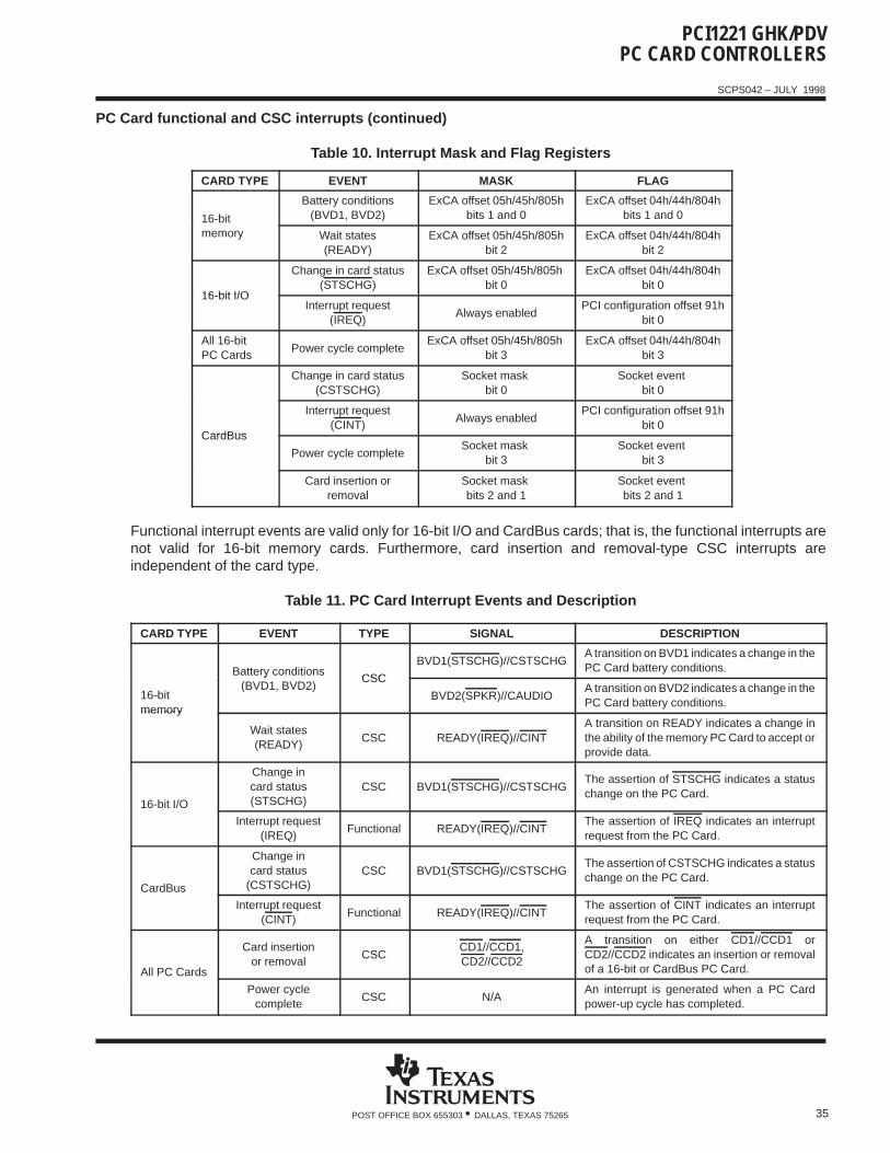
PCI1221 GHK/PDVPC CARD CONTROLLERS
SCPS042 – JULY 1998
35POST OFFICE BOX 655303 • DALLAS, TEXAS 75265
PC Card functional and CSC interrupts (continued)
Table 10. Interrupt Mask and Flag Registers
CARD TYPE EVENT MASK FLAG
16-bit
Battery conditions(BVD1, BVD2)
ExCA offset 05h/45h/805hbits 1 and 0
ExCA offset 04h/44h/804hbits 1 and 0
memory Wait states(READY)
ExCA offset 05h/45h/805hbit 2
ExCA offset 04h/44h/804hbit 2
16 bit I/O
Change in card status(STSCHG)
ExCA offset 05h/45h/805h bit 0
ExCA offset 04h/44h/804hbit 0
16-bit I/OInterrupt request
(IREQ)Always enabled
PCI configuration offset 91hbit 0
All 16-bitPC Cards
Power cycle completeExCA offset 05h/45h/805h
bit 3ExCA offset 04h/44h/804h
bit 3
Change in card status(CSTSCHG)
Socket mask bit 0
Socket event bit 0
CardBus
Interrupt request(CINT)
Always enabledPCI configuration offset 91h
bit 0CardBus
Power cycle completeSocket mask
bit 3Socket event
bit 3
Card insertion orremoval
Socket mask bits 2 and 1
Socket event bits 2 and 1
Functional interrupt events are valid only for 16-bit I/O and CardBus cards; that is, the functional interrupts arenot valid for 16-bit memory cards. Furthermore, card insertion and removal-type CSC interrupts areindependent of the card type.
Table 11. PC Card Interrupt Events and Description
CARD TYPE EVENT TYPE SIGNAL DESCRIPTION
Battery conditionsCSC
BVD1(STSCHG)//CSTSCHGA transition on BVD1 indicates a change in thePC Card battery conditions.
16-bitmemory
y(BVD1, BVD2)
CSC
BVD2(SPKR)//CAUDIOA transition on BVD2 indicates a change in thePC Card battery conditions.
memory
Wait states(READY)
CSC READY(IREQ)//CINTA transition on READY indicates a change inthe ability of the memory PC Card to accept orprovide data.
16-bit I/O
Change incard status(STSCHG)
CSC BVD1(STSCHG)//CSTSCHGThe assertion of STSCHG indicates a statuschange on the PC Card.
Interrupt request(IREQ)
Functional READY(IREQ)//CINTThe assertion of IREQ indicates an interruptrequest from the PC Card.
CardBus
Change incard status
(CSTSCHG)CSC BVD1(STSCHG)//CSTSCHG
The assertion of CSTSCHG indicates a statuschange on the PC Card.
Interrupt request(CINT)
Functional READY(IREQ)//CINTThe assertion of CINT indicates an interruptrequest from the PC Card.
All PC Cards
Card insertionor removal
CSCCD1//CCD1,CD2//CCD2
A transition on either CD1//CCD1 orCD2//CCD2 indicates an insertion or removalof a 16-bit or CardBus PC Card.
Power cyclecomplete
CSC N/AAn interrupt is generated when a PC Cardpower-up cycle has completed.
PCI1221 GHK/PDVPC CARD CONTROLLERS
SCPS042 – JULY 1998
36 POST OFFICE BOX 655303 • DALLAS, TEXAS 75265
PC Card functional and CSC interrupts (continued)
The naming convention for PC Card signals describes the function for 16-bit memory, I/O cards, and CardBus.For example, READY(IREQ)//CINT includes READY for 16-bit memory cards, IREQ for 16-bit I/O cards, andCINT for CardBus cards. The 16-bit memory card signal name is first, with the I/O card signal name second,enclosed in parentheses. The CardBus signal name follows after a forward double slash (//).
The PC Card standard describes the power-up sequence that must be followed by the PCI1221 when aninsertion event occurs and the host requests that the socket VCC and VPP be powered. Upon completion of thispower-up sequence, the PCI1221 interrupt scheme can be used to notify the host system (see Table 11),denoted by the power cycle complete event. This interrupt source is considered a PCI1221 internal eventbecause it depends on the completion of applying power to the socket rather than on a signal change at the PCCard interface.
interrupt masks and flags
Host software may individually mask (or disable) most of the potential interrupt sources listed in Table 11 bysetting the appropriate bits in the PCI1221. By individually masking the interrupt sources listed, software cancontrol those events that cause a PCI1221 interrupt. Host software has some control over the system interruptthe PCI1221 asserts by programming the appropriate routing registers. The PCI1221 allows host software toroute PC Card CSC and PC Card functional interrupts to separate system interrupts. Interrupt routing somewhatspecific to the interrupt signaling method used is discussed in more detail in the following sections.
When an interrupt is signaled by the PCI1221, the interrupt service routine must determine which of the eventslisted in Table 10 caused the interrupt. Internal registers in the PCI1221 provide flags that report the source ofan interrupt. By reading these status bits, the interrupt service routine can determine the action to be taken.
Table 10 details the registers and bits associated with masking and reporting potential interrupts. All interruptscan be masked except the functional PC Card interrupts, and an interrupt status flag is available for all typesof interrupts.
Notice that there is not a mask bit to stop the PCI1221 from passing PC Card functional interrupts through tothe appropriate interrupt scheme. These interrupts are not valid until the card is properly powered, and thereshould never be a card interrupt that does not require service after proper initialization.
Various methods of clearing the interrupt flag bits are listed in Table 10. The flag bits in the ExCA registers (16-bitPC Card-related interrupt flags) can be cleared using two different methods. One method is an explicit write of1 to the flag bit to clear, and the other is by reading the flag bit register. The selection of flag bit clearing is madeby bit 2 in the global control register (ExCA offset 1Eh/5Eh/81Eh), and defaults to the flag cleared onread method.
The CardBus-related interrupt flags can be cleared by an explicit write of 1 to the interrupt flag in the socket eventregister. Although some of the functionality is shared between the CardBus registers and the ExCA registers,software should not program the chip through both register sets when a CardBus card is functioning.
using parallel IRQ interrupts
The seven multifunction terminals, MFUNC6:0, implemented in the PCI1221 may be routed to obtain a subsetof the ISA IRQs . The IRQ choices provide ultimate flexibility in PC Card host interruptions. To use the parallelISA type IRQ interrupt signaling, software must program the device control register, located at PCI offset 92h,to select the parallel IRQ signaling scheme. Refer to the multifunction routing register description on page 62for details on configuring the multifunction terminals.
A system using parallel IRQs requires (at a minimum) one PCI terminal, INTA, to signal CSC events. Thisrequirement is dictated by certain card and socket services software. The INTA requirement calls for routingthe MFUNC0 terminal for INTA signaling. The INTRTIE bit is used, in this case, to route socket 1 interrupt eventsto INTA. This leaves (at a maximum) six different IRQs to support legacy 16-bit PC Card functions.
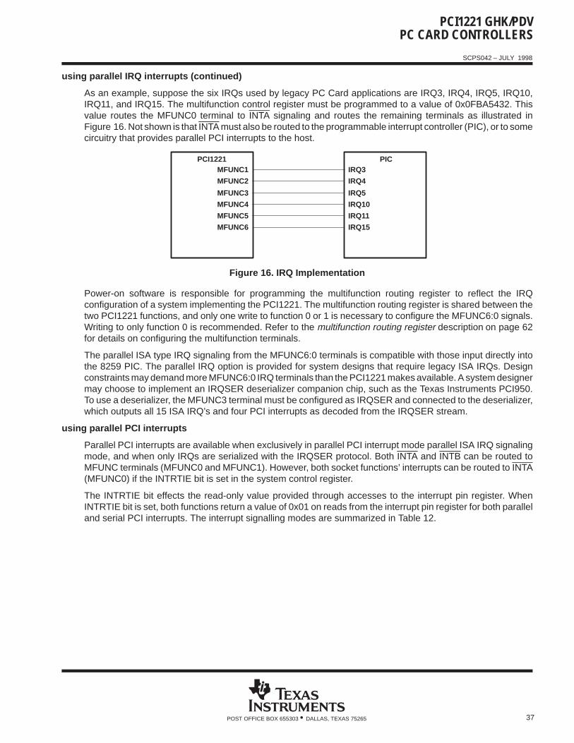
PCI1221 GHK/PDVPC CARD CONTROLLERS
SCPS042 – JULY 1998
37POST OFFICE BOX 655303 • DALLAS, TEXAS 75265
using parallel IRQ interrupts (continued)
As an example, suppose the six IRQs used by legacy PC Card applications are IRQ3, IRQ4, IRQ5, IRQ10,IRQ11, and IRQ15. The multifunction control register must be programmed to a value of 0x0FBA5432. Thisvalue routes the MFUNC0 terminal to INTA signaling and routes the remaining terminals as illustrated inFigure 16. Not shown is that INTA must also be routed to the programmable interrupt controller (PIC), or to somecircuitry that provides parallel PCI interrupts to the host.
PCI1221 PICMFUNC1
MFUNC2
MFUNC3
MFUNC4
MFUNC5
MFUNC6
IRQ3
IRQ4
IRQ5
IRQ10
IRQ11
IRQ15
Figure 16. IRQ Implementation
Power-on software is responsible for programming the multifunction routing register to reflect the IRQconfiguration of a system implementing the PCI1221. The multifunction routing register is shared between thetwo PCI1221 functions, and only one write to function 0 or 1 is necessary to configure the MFUNC6:0 signals.Writing to only function 0 is recommended. Refer to the multifunction routing register description on page 62for details on configuring the multifunction terminals.
The parallel ISA type IRQ signaling from the MFUNC6:0 terminals is compatible with those input directly intothe 8259 PIC. The parallel IRQ option is provided for system designs that require legacy ISA IRQs. Designconstraints may demand more MFUNC6:0 IRQ terminals than the PCI1221 makes available. A system designermay choose to implement an IRQSER deserializer companion chip, such as the Texas Instruments PCI950.To use a deserializer, the MFUNC3 terminal must be configured as IRQSER and connected to the deserializer,which outputs all 15 ISA IRQ’s and four PCI interrupts as decoded from the IRQSER stream.
using parallel PCI interrupts
Parallel PCI interrupts are available when exclusively in parallel PCI interrupt mode parallel ISA IRQ signalingmode, and when only IRQs are serialized with the IRQSER protocol. Both INTA and INTB can be routed toMFUNC terminals (MFUNC0 and MFUNC1). However, both socket functions’ interrupts can be routed to INTA(MFUNC0) if the INTRTIE bit is set in the system control register.
The INTRTIE bit effects the read-only value provided through accesses to the interrupt pin register. WhenINTRTIE bit is set, both functions return a value of 0x01 on reads from the interrupt pin register for both paralleland serial PCI interrupts. The interrupt signalling modes are summarized in Table 12.
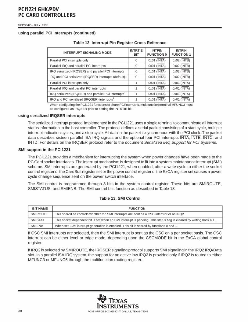
PCI1221 GHK/PDVPC CARD CONTROLLERS
SCPS042 – JULY 1998
38 POST OFFICE BOX 655303 • DALLAS, TEXAS 75265
using parallel PCI interrupts (continued)
Table 12. Interrupt Pin Register Cross Reference
INTERRUPT SIGNALING MODEINTRTIE
BITINTPIN
FUNCTION 0INTPIN
FUNCTION 1
Parallel PCI interrupts only 0 0x01 (INTA) 0x02 (INTB)
Parallel IRQ and parallel PCI interrupts 0 0x01 (INTA) 0x02 (INTB)
IRQ serialized (IRQSER) and parallel PCI interrupts 0 0x01 (INTA) 0x02 (INTB)
IRQ and PCI serialized (IRQSER) interrupts (default) 0 0x01 (INTA) 0x02 (INTB)
Parallel PCI interrupts only 1 0x01 (INTA) 0x01 (INTA)
Parallel IRQ and parallel PCI interrupts 1 0x01 (INTA) 0x01 (INTA)
IRQ serialized (IRQSER) and parallel PCI interrupts† 1 0x01 (INTA) 0x01 (INTA)
IRQ and PCI serialized (IRQSER) interrupts† 1 0x01 (INTA) 0x01 (INTA)† When configuring the PCI1221 functions to share PCI interrupts, multifunction terminal MFUNC3 must
be configured as IRQSER prior to setting the INTRTIE bit.
using serialized IRQSER interrupts
The serialized interrupt protocol implemented in the PCI1221 uses a single terminal to communicate all interruptstatus information to the host controller. The protocol defines a serial packet consisting of a start cycle, multipleinterrupt indication cycles, and a stop cycle. All data in the packet is synchronous with the PCI clock. The packetdata describes sixteen parallel ISA IRQ signals and the optional four PCI interrupts INTA, INTB, INTC, andINTD. For details on the IRQSER protocol refer to the document Serialized IRQ Support for PCI Systems.
SMI support in the PCI1221
The PCI1221 provides a mechanism for interrupting the system when power changes have been made to thePC Card socket interfaces. The interrupt mechanism is designed to fit into a system maintenance interrupt (SMI)scheme. SMI interrupts are generated by the PCI1221, when enabled, after a write cycle to either the socketcontrol register of the CardBus register set or the power control register of the ExCA register set causes a powercycle change sequence sent on the power switch interface.
The SMI control is programmed through 3 bits in the system control register. These bits are SMIROUTE,SMISTATUS, and SMIENB. The SMI control bits function as described in Table 13.
Table 13. SMI Control
BIT NAME FUNCTION
SMIROUTE This shared bit controls whether the SMI interrupts are sent as a CSC interrupt or as IRQ2.
SMISTAT This socket dependent bit is set when an SMI interrupt is pending. This status flag is cleared by writing back a 1.
SMIENB When set, SMI interrupt generation is enabled. This bit is shared by functions 0 and 1.
If CSC SMI interrupts are selected, then the SMI interrupt is sent as the CSC on a per socket basis. The CSCinterrupt can be either level or edge mode, depending upon the CSCMODE bit in the ExCA global controlregister.
If IRQ2 is selected by SMIROUTE, the IRQSER signaling protocol supports SMI signaling in the IRQ2 IRQ/Dataslot. In a parallel ISA IRQ system, the support for an active low IRQ2 is provided only if IRQ2 is routed to eitherMFUNC3 or MFUNC6 through the multifunction routing register.
PCI1221 GHK/PDVPC CARD CONTROLLERS
SCPS042 – JULY 1998
39POST OFFICE BOX 655303 • DALLAS, TEXAS 75265
power management overview
TI has expended great effort to provide a high-performance device with low power consumption. In addition tothe low-power CMOS technology process used for the PCI1221, various features are designed into the deviceto allow implementation of popular power-saving techniques. These features and techniques are discussed inthis section.
clock run protocol
The PCI CLKRUN feature is the primary method of power management on the PCI interface of the PCI1221.CLKRUN signalling is provided through the MFUNC6 terminal. Since some chip sets do not implementCLKRUN, this is not always available to the system designer, and alternate power savings features areprovided. For details on the CLKRUN protocol refer to the PCI Mobile Design Guide.
The PCI1221 does not permit the central resource to stop the PCI clock under any of the following conditions:
The KEEPCLK bit in the system control register is set. The PC Card-16 resource manager is busy. The PCI1221 CardBus master state machine is busy. A cycle may be in progress on CardBus. The PCI1221 master is busy. There may be posted data from CardBus to PCI in the PCI1221. There are pending interrupts. The CardBus CCLK for either socket has not been stopped by the PCI1221 CLKRUN manager.
The PCI1221 restarts the PCI clock using the CLKRUN protocol under any of the following conditions:
A PC Card-16 IREQ or a CardBus CINT has been asserted by either card. A CardBus wakeup (CSTSCHG) or PC Card-16 STSCHG/RI event occurs in either socket. A CardBus attempts to start the CCLK using CCLKRUN. A CardBus card arbitrates for the CardBus bus using CREQ.
CardBus PC card power management
The PCI1221 implements its own card power management engine that can be used to turn off the CCLK to asocket when there is no activity to the CardBus PC Card. The PCI clock-run protocol is followed on the CardBusCCLKRUN interface to control this clock management.
16-Bit PC card power mManagement
The COE and PWRDOWN bits in the ExCA registers are provided for 16-bit PC Card power management. TheCOE bit three states the card interface to save power. The power savings when using this feature are minimal.The COE bit will reset the PC Card when used, and the PWRDOWN bit will not. Furthermore, the PWRDOWNbit is an automatic COE, that is, the PWRDOWN performs the COE function when there is no card activity.
NOTE:The 16-bit PC Card must implement the proper pullup resistors for the COE and PWRDOWNmodes.
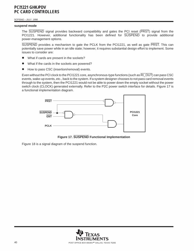
PCI1221 GHK/PDVPC CARD CONTROLLERS
SCPS042 – JULY 1998
40 POST OFFICE BOX 655303 • DALLAS, TEXAS 75265
suspend mode
The SUSPEND signal provides backward compatibility and gates the PCI reset (PRST) signal from thePCI1221. However, additional functionality has been defined for SUSPEND to provide additionalpower-management options.
SUSPEND provides a mechanism to gate the PCLK from the PCI1221, as well as gate PRST. This canpotentially save power while in an idle state; however, it requires substantial design effort to implement. Someissues to consider are:
What if cards are present in the sockets?
What if the cards in the sockets are powered?
How to pass CSC (insertion/removal) events.
Even without the PCI clock to the PCI1221 core, asynchronous-type functions (such as RI_OUT) can pass CSCevents, wake-up events, etc., back to the system. If a system designer chooses to not pass card removal eventsthrough to the system, then the PCI1221 would not be able to power down the empty socket without the powerswitch clock (CLOCK) generated externally. Refer to the P2C power switch interface for details. Figure 17 isa functional implementation diagram.
PCI1221Core
SUSPEND
PRST
GNT
PCLK
Figure 17. SUSPEND Functional Implementation
Figure 18 is a signal diagram of the suspend function.
PCI1221 GHK/PDVPC CARD CONTROLLERS
SCPS042 – JULY 1998
41POST OFFICE BOX 655303 • DALLAS, TEXAS 75265
suspend mode (continued)
PRST
GNT
SUSPEND
PCLK
PRSTIN
SUSPENDIN
PCLKIN
External Terminals
Internal Signals
Figure 18. Signal Diagram of Suspend Function
ring indicate
The RI_OUT output is an important feature in power management, allowing a system to go into a suspendedmode and wake up on modem rings and other card events. TI designed flexibility permits this signal to fit wideplatform requirements. RI_OUT on the PCI1221 can be asserted under any of the following conditions:
A 16-bit PC Card modem in a powered socket asserts RI to indicate to the system the presence of anincoming call.
A powered down CardBus card asserts CSTSCHG (CBWAKE) requesting system and interface wake up.
A CSC event occurs, such as insertion/removal of cards, battery voltage levels.
CSTSCHG from a powered CardBus card is indicated as a CSC event, not as a CBWAKE event. These twoRI_OUT events are enabled separately. Figure 15 shows various enable bits for the PCI1221 RI_OUT function;however, it does not show the masking of CSC events. See Table 10 for a detailed description of CSC interruptmasks and flags.
PCI1221 GHK/PDVPC CARD CONTROLLERS
SCPS042 – JULY 1998
42 POST OFFICE BOX 655303 • DALLAS, TEXAS 75265
ring indicate (continued)
CardI/F
PC CardSocket 0
CSC
CSTSMASK
RIENB
RI_OUT
RI_OUT Function
RINGEN
CDRESUME
CSC
RI
CardI/F
PC CardSocket 1
CSC
CSTSMASK
RINGEN
CDRESUME
CSC
RI
Figure 19. RI_OUT Functional Diagram
RI from the 16-bit PC Card interface is masked by the ExCA control bit RINGEN in the interrupt and generalcontrol register. This is programmed on a per-socket basis and is only applicable when a 16-bit card is poweredin the socket.
The CBWAKE signaling to RI_OUT is enabled through the same mask as the CSC event for CSTSCHG. Themask bit, CSTSMASK, is programmed through the socket mask register in the CardBus socket registers.
PCI power management (PCIPM)
The PCI power-management (PCIPM) specification establishes the infrastructure required to let the operatingsystem control the power of PCI functions. This is done by defining a standard PCI interface and operations tomanage the power of PCI functions on the bus. The PCI bus and the PCI functions can be assigned one of foursoftware-visible power-management states that result in varying levels of power savings.
The four power-management states of PCI functions are:
D0 - Fully-on state
D1 and D2 - Intermediate states
D3 - Off state
Similarly, bus power states of the PCI bus are B0-B3. The bus power states B0-B3 are derived from the devicepower state of the originating bridge device.
For the operating system (OS) to power manage the device power states on the PCI bus, the PCI function shouldsupport four power-management operations. These operations are:
Capabilities reporting Power status reporting Setting the power state System wake up
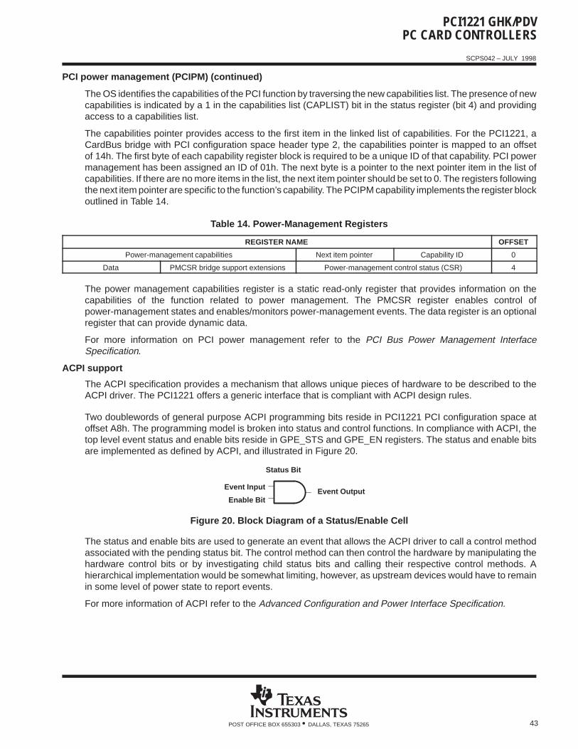
PCI1221 GHK/PDVPC CARD CONTROLLERS
SCPS042 – JULY 1998
43POST OFFICE BOX 655303 • DALLAS, TEXAS 75265
PCI power management (PCIPM) (continued)
The OS identifies the capabilities of the PCI function by traversing the new capabilities list. The presence of newcapabilities is indicated by a 1 in the capabilities list (CAPLIST) bit in the status register (bit 4) and providingaccess to a capabilities list.
The capabilities pointer provides access to the first item in the linked list of capabilities. For the PCI1221, aCardBus bridge with PCI configuration space header type 2, the capabilities pointer is mapped to an offsetof 14h. The first byte of each capability register block is required to be a unique ID of that capability. PCI powermanagement has been assigned an ID of 01h. The next byte is a pointer to the next pointer item in the list ofcapabilities. If there are no more items in the list, the next item pointer should be set to 0. The registers followingthe next item pointer are specific to the function’s capability. The PCIPM capability implements the register blockoutlined in Table 14.
Table 14. Power-Management Registers
REGISTER NAME OFFSET
Power-management capabilities Next item pointer Capability ID 0
Data PMCSR bridge support extensions Power-management control status (CSR) 4
The power management capabilities register is a static read-only register that provides information on thecapabilities of the function related to power management. The PMCSR register enables control ofpower-management states and enables/monitors power-management events. The data register is an optionalregister that can provide dynamic data.
For more information on PCI power management refer to the PCI Bus Power Management InterfaceSpecification.
ACPI support
The ACPI specification provides a mechanism that allows unique pieces of hardware to be described to theACPI driver. The PCI1221 offers a generic interface that is compliant with ACPI design rules.
Two doublewords of general purpose ACPI programming bits reside in PCI1221 PCI configuration space atoffset A8h. The programming model is broken into status and control functions. In compliance with ACPI, thetop level event status and enable bits reside in GPE_STS and GPE_EN registers. The status and enable bitsare implemented as defined by ACPI, and illustrated in Figure 20.
Status Bit
Event OutputEvent Input
Enable Bit
Figure 20. Block Diagram of a Status/Enable Cell
The status and enable bits are used to generate an event that allows the ACPI driver to call a control methodassociated with the pending status bit. The control method can then control the hardware by manipulating thehardware control bits or by investigating child status bits and calling their respective control methods. Ahierarchical implementation would be somewhat limiting, however, as upstream devices would have to remainin some level of power state to report events.
For more information of ACPI refer to the Advanced Configuration and Power Interface Specification.
PCI1221 GHK/PDVPC CARD CONTROLLERS
SCPS042 – JULY 1998
44 POST OFFICE BOX 655303 • DALLAS, TEXAS 75265
PC Card controller programming model
This section describes the PCI1221 PCI configuration registers that make up the 256-byte PCI configurationheader for each PCI1221 function. As noted, some bits are global in nature and should be accessed onlythrough function 0.
PCI configuration registers (functions 0 and 1)
The PCI1221 is a multifunction PCI device, and the PC Card controller is integrated as PCI functions 0 and 1.The configuration header is compliant with the PCI specification as a CardBus bridge header and is PC 99compliant as well. Table 15 shows the PCI configuration header, which includes both the predefined portion ofthe configuration space and the user-definable registers.
Table 15. PCI Configuration Registers (Functions 0 and 1)
REGISTER NAME OFFSET
Device ID Vendor ID 00h
Status Command 04h
Class code Revision ID 08h
BIST Header type Latency timer Cache line size 0Ch
CardBus socket/ExCA base address 10h
Secondary status Reserved Capability pointer 14h
CardBus latency timer Subordinate bus number CardBus bus number PCI bus number 18h
CardBus Memory base register 0 1Ch
CardBus Memory limit register 0 20h
CardBus Memory base register 1 24h
CardBus Memory limit register 1 28h
CardBus I/O base register 0 2Ch
CardBus I/O limit register 0 30h
CardBus I/O base register 1 34h
CardBus I/O limit register 1 38h
Bridge control Interrupt pin Interrupt line 3Ch
Subsystem ID Subsystem vendor ID 40h
PC Card 16-bit I/F legacy-mode base address 44h
Reserved 48h–7Ch
System control 80h
Reserved 84h–88h
Multifunction routing 8Ch
Diagnostic Device control Card control Retry status 90h
Reserved 94h-9Fh
Power-management capabilities Next-item pointer Capability ID A0h
PM dataPMCSR bridge support
extensionsPower-management control/status A4h
General-purpose event enable General-purpose event status A8h
General-purpose output General-purpose input ACh
Serial bus control/status Serial bus slave address Serial bus index Serial bus data B0h
Reserved B4h–FCh
PCI1221 GHK/PDVPC CARD CONTROLLERS
SCPS042 – JULY 1998
45POST OFFICE BOX 655303 • DALLAS, TEXAS 75265
vendor ID registerBit 15 14 13 12 11 10 9 8 7 6 5 4 3 2 1 0
Name Vendor ID
Type R R R R R R R R R R R R R R R R
Default 0 0 0 1 0 0 0 0 0 1 0 0 1 1 0 0
Register: Vendor IDType: Read onlyOffset: 00h (functions 0, 1)Default: 104ChDescription: This 16-bit read-only register contains a value allocated by the PCI SIG (special interest
group) and identifies the manufacturer of the PCI device. The vendor ID assigned to TI is104Ch.
device ID registerBit 15 14 13 12 11 10 9 8 7 6 5 4 3 2 1 0
Name Device ID
Type R R R R R R R R R R R R R R R R
Default 1 0 1 0 1 1 0 0 0 0 0 1 1 0 0 1
Register: Device IDType: Read onlyOffset: 02h (functions 0, 1)Default: AC19hDescription: This 16-bit read-only register contains a value assigned to the PCI1221 by TI. The device
identification for the PCI1221 is AC19h.
command registerBit 15 14 13 12 11 10 9 8 7 6 5 4 3 2 1 0
Name Command
Type R R R R R R R R/W R R/W R R R R/W R/W R/W
Default 0 0 0 0 0 0 0 0 0 0 0 0 0 0 0 0
Register: CommandType: Read only, read/write (see individual bit descriptions)Offset: 04hDefault: 0000hDescription: The command register provides control over the PCI1221 interface to the PCI bus. All bit
functions adhere to the definitions in PCI Local Bus Specification 2.2. None of the bit functionsin this register are shared between the two PCI1221 PCI functions. Two command registersexist in the PCI1221, one for each function. Software must manipulate the two PCI1221functions as separate entities when enabling functionality through the command register. TheSERR_EN and PERR_EN enable bits in this register are internally wired-OR between the twofunctions, and these control bits appear separately according to their software function. SeeTable 16 for the complete description of the register contents.
PCI1221 GHK/PDVPC CARD CONTROLLERS
SCPS042 – JULY 1998
46 POST OFFICE BOX 655303 • DALLAS, TEXAS 75265
Table 16. Command Register
BIT SIGNAL TYPE FUNCTION
15–10 RSVD R Reserved. Bits 15–10 are read only and return 0s when read. Write transactions have no effect.
9 FBB_EN RFast back-to-back enable. The PCI1221 does not generate fast back-to-back transactions; therefore, bit9 is read only and returns 0s when read.
8 SERR_EN R/W
System Error (SERR) enable. Bit 8 controls the enable for the SERR driver on the PCI interface. SERRcan be asserted after detecting an address parity error on the PCI bus. Both bit 8 and bit 6 must be setfor the PCI1221 to report address parity errors.
0 = Disable SERR output driver (default)1 = Enable SERR output driver
7 STEP_EN RAddress/data stepping control. The PCI1221 does not support address/data stepping, and bit 7 ishardwired to 0. Write transactions to this bit have no effect.
6 PERR_EN R/W
Parity error response enable. Bit 6 controls the PCI1221’s response to parity errors through PERR. Dataparity errors are indicated by asserting PERR, whereas address parity errors are indicated by assertingSERR.
0 = PCI1221 ignores detected parity error (default)1 = PCI1221 responds to detected parity errors
5 VGA_EN RVGA palette snoop. Bit 5 controls how PCI devices handle accesses to video graphics array (VGA) paletteregisters. The PCI1221 does not support VGA palette snooping; therefore, this bit is hardwired to 0. Bit5 is read only and returns 0 when read. Write transactions to this bit have no effect.
4 MWI_EN R
Memory write and invalidate enable. Bit 4 controls whether a PCI initiator device can generate memorywrite and Invalidate commands. The PCI1221 controller does not support memory write and invalidatecommands, it uses memory write commands instead; therefore, this bit is hardwired to 0. Bit 4 is read onlyand returns 0 when read. Write transactions to this bit have no effect.
3 SPECIAL RSpecial cycles. Bit 3 controls whether or not a PCI device ignores PCI special cycles. The PCI1221 doesnot respond to special cycle operations; therefore, this bit is hardwired to 0. Bit 3 is read only and returns0 when read. Write transactions to this bit have no effect.
2 MAST_EN R/W
Bus master control. Bit 2 controls whether or not the PCI1221 can act as a PCI bus initiator (master). ThePCI1221 can take control of the PCI bus only when this bit is set.
0 = Disables the PCI1221’s ability to generate PCI bus accesses (default)1 = Enables the PCI1221’s ability to generate PCI bus accesses
1 MEM_EN R/WMemory space enable. Bit 1 controls whether or not the PCI1221 can claim cycles in PCI memory space.
0 = Disables the PCI1221’s response to memory space accesses (default)1 = Enables the PCI1221’s response to memory space accesses
0 IO_EN R/WI/O space control. Bit 0 controls whether or not the PCI1221 can claim cycles in PCI I/O space.
0 = Disables the PCI1221 from responding to I/O space accesses (default)1 = Enables the PCI1221 to respond to I/O space accesses
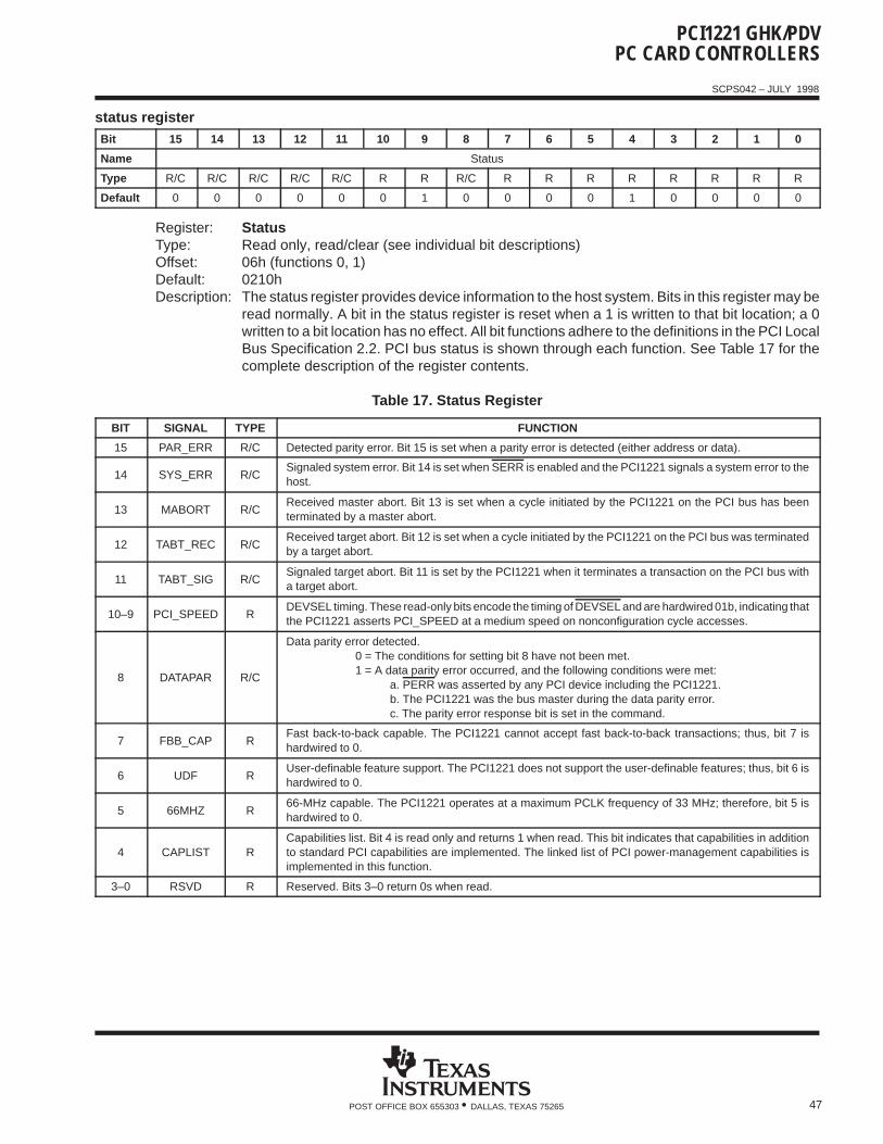
PCI1221 GHK/PDVPC CARD CONTROLLERS
SCPS042 – JULY 1998
47POST OFFICE BOX 655303 • DALLAS, TEXAS 75265
status registerBit 15 14 13 12 11 10 9 8 7 6 5 4 3 2 1 0
Name Status
Type R/C R/C R/C R/C R/C R R R/C R R R R R R R R
Default 0 0 0 0 0 0 1 0 0 0 0 1 0 0 0 0
Register: StatusType: Read only, read/clear (see individual bit descriptions)Offset: 06h (functions 0, 1)Default: 0210hDescription: The status register provides device information to the host system. Bits in this register may be
read normally. A bit in the status register is reset when a 1 is written to that bit location; a 0written to a bit location has no effect. All bit functions adhere to the definitions in the PCI LocalBus Specification 2.2. PCI bus status is shown through each function. See Table 17 for thecomplete description of the register contents.
Table 17. Status Register
BIT SIGNAL TYPE FUNCTION
15 PAR_ERR R/C Detected parity error. Bit 15 is set when a parity error is detected (either address or data).
14 SYS_ERR R/CSignaled system error. Bit 14 is set when SERR is enabled and the PCI1221 signals a system error to thehost.
13 MABORT R/CReceived master abort. Bit 13 is set when a cycle initiated by the PCI1221 on the PCI bus has beenterminated by a master abort.
12 TABT_REC R/CReceived target abort. Bit 12 is set when a cycle initiated by the PCI1221 on the PCI bus was terminatedby a target abort.
11 TABT_SIG R/CSignaled target abort. Bit 11 is set by the PCI1221 when it terminates a transaction on the PCI bus witha target abort.
10–9 PCI_SPEED RDEVSEL timing. These read-only bits encode the timing of DEVSEL and are hardwired 01b, indicating thatthe PCI1221 asserts PCI_SPEED at a medium speed on nonconfiguration cycle accesses.
8 DATAPAR R/C
Data parity error detected.0 = The conditions for setting bit 8 have not been met.1 = A data parity error occurred, and the following conditions were met:
a. PERR was asserted by any PCI device including the PCI1221.b. The PCI1221 was the bus master during the data parity error.c. The parity error response bit is set in the command.
7 FBB_CAP RFast back-to-back capable. The PCI1221 cannot accept fast back-to-back transactions; thus, bit 7 ishardwired to 0.
6 UDF RUser-definable feature support. The PCI1221 does not support the user-definable features; thus, bit 6 ishardwired to 0.
5 66MHZ R66-MHz capable. The PCI1221 operates at a maximum PCLK frequency of 33 MHz; therefore, bit 5 ishardwired to 0.
4 CAPLIST RCapabilities list. Bit 4 is read only and returns 1 when read. This bit indicates that capabilities in additionto standard PCI capabilities are implemented. The linked list of PCI power-management capabilities isimplemented in this function.
3–0 RSVD R Reserved. Bits 3–0 return 0s when read.
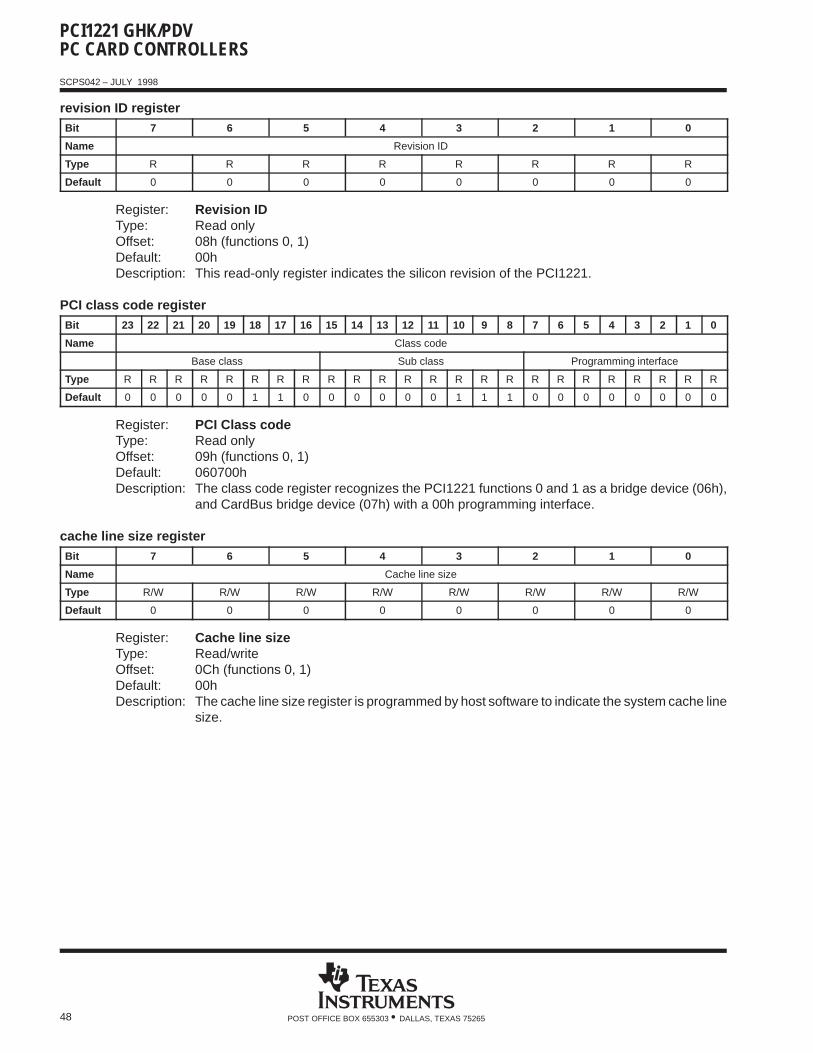
PCI1221 GHK/PDVPC CARD CONTROLLERS
SCPS042 – JULY 1998
48 POST OFFICE BOX 655303 • DALLAS, TEXAS 75265
revision ID registerBit 7 6 5 4 3 2 1 0
Name Revision ID
Type R R R R R R R R
Default 0 0 0 0 0 0 0 0
Register: Revision IDType: Read onlyOffset: 08h (functions 0, 1)Default: 00hDescription: This read-only register indicates the silicon revision of the PCI1221.
PCI class code registerBit 23 22 21 20 19 18 17 16 15 14 13 12 11 10 9 8 7 6 5 4 3 2 1 0
Name Class code
Base class Sub class Programming interface
Type R R R R R R R R R R R R R R R R R R R R R R R R
Default 0 0 0 0 0 1 1 0 0 0 0 0 0 1 1 1 0 0 0 0 0 0 0 0
Register: PCI Class codeType: Read onlyOffset: 09h (functions 0, 1)Default: 060700hDescription: The class code register recognizes the PCI1221 functions 0 and 1 as a bridge device (06h),
and CardBus bridge device (07h) with a 00h programming interface.
cache line size registerBit 7 6 5 4 3 2 1 0
Name Cache line size
Type R/W R/W R/W R/W R/W R/W R/W R/W
Default 0 0 0 0 0 0 0 0
Register: Cache line sizeType: Read/writeOffset: 0Ch (functions 0, 1)Default: 00hDescription: The cache line size register is programmed by host software to indicate the system cache line
size.
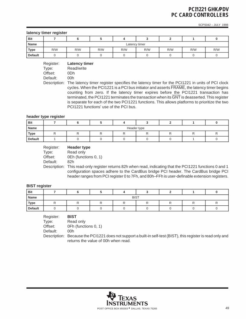
PCI1221 GHK/PDVPC CARD CONTROLLERS
SCPS042 – JULY 1998
49POST OFFICE BOX 655303 • DALLAS, TEXAS 75265
latency timer registerBit 7 6 5 4 3 2 1 0
Name Latency timer
Type R/W R/W R/W R/W R/W R/W R/W R/W
Default 0 0 0 0 0 0 0 0
Register: Latency timerType: Read/writeOffset: 0DhDefault: 00hDescription: The latency timer register specifies the latency timer for the PCI1221 in units of PCI clock
cycles. When the PCI1221 is a PCI bus initiator and asserts FRAME, the latency timer beginscounting from zero. If the latency timer expires before the PCI1221 transaction hasterminated, the PCI1221 terminates the transaction when its GNT is deasserted. This registeris separate for each of the two PCI1221 functions. This allows platforms to prioritize the twoPCI1221 functions’ use of the PCI bus.
header type registerBit 7 6 5 4 3 2 1 0
Name Header type
Type R R R R R R R R
Default 1 0 0 0 0 0 1 0
Register: Header typeType: Read onlyOffset: 0Eh (functions 0, 1)Default: 82hDescription: This read-only register returns 82h when read, indicating that the PCI1221 functions 0 and 1
configuration spaces adhere to the CardBus bridge PCI header. The CardBus bridge PCIheader ranges from PCI register 0 to 7Fh, and 80h–FFh is user-definable extension registers.
BIST registerBit 7 6 5 4 3 2 1 0
Name BIST
Type R R R R R R R R
Default 0 0 0 0 0 0 0 0
Register: BISTType: Read onlyOffset: 0Fh (functions 0, 1)Default: 00hDescription: Because the PCI1221 does not support a built-in self-test (BIST), this register is read only and
returns the value of 00h when read.
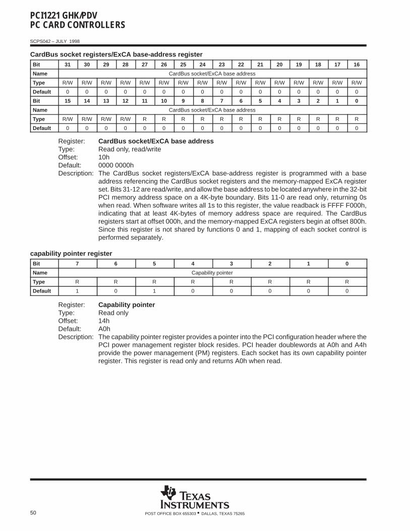
PCI1221 GHK/PDVPC CARD CONTROLLERS
SCPS042 – JULY 1998
50 POST OFFICE BOX 655303 • DALLAS, TEXAS 75265
CardBus socket registers/ExCA base-address registerBit 31 30 29 28 27 26 25 24 23 22 21 20 19 18 17 16
Name CardBus socket/ExCA base address
Type R/W R/W R/W R/W R/W R/W R/W R/W R/W R/W R/W R/W R/W R/W R/W R/W
Default 0 0 0 0 0 0 0 0 0 0 0 0 0 0 0 0
Bit 15 14 13 12 11 10 9 8 7 6 5 4 3 2 1 0
Name CardBus socket/ExCA base address
Type R/W R/W R/W R/W R R R R R R R R R R R R
Default 0 0 0 0 0 0 0 0 0 0 0 0 0 0 0 0
Register: CardBus socket/ExCA base addressType: Read only, read/writeOffset: 10hDefault: 0000 0000hDescription: The CardBus socket registers/ExCA base-address register is programmed with a base
address referencing the CardBus socket registers and the memory-mapped ExCA registerset. Bits 31-12 are read/write, and allow the base address to be located anywhere in the 32-bitPCI memory address space on a 4K-byte boundary. Bits 11-0 are read only, returning 0swhen read. When software writes all 1s to this register, the value readback is FFFF F000h,indicating that at least 4K-bytes of memory address space are required. The CardBusregisters start at offset 000h, and the memory-mapped ExCA registers begin at offset 800h.Since this register is not shared by functions 0 and 1, mapping of each socket control isperformed separately.
capability pointer registerBit 7 6 5 4 3 2 1 0
Name Capability pointer
Type R R R R R R R R
Default 1 0 1 0 0 0 0 0
Register: Capability pointerType: Read onlyOffset: 14hDefault: A0hDescription: The capability pointer register provides a pointer into the PCI configuration header where the
PCI power management register block resides. PCI header doublewords at A0h and A4hprovide the power management (PM) registers. Each socket has its own capability pointerregister. This register is read only and returns A0h when read.
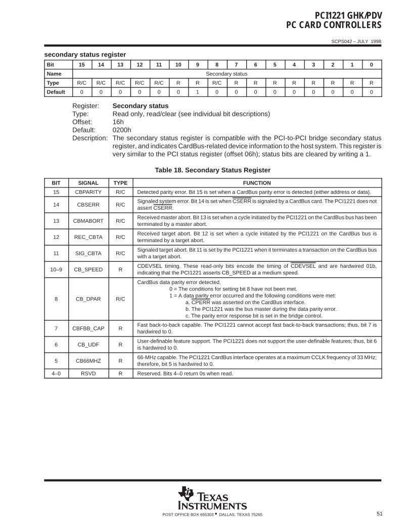
PCI1221 GHK/PDVPC CARD CONTROLLERS
SCPS042 – JULY 1998
51POST OFFICE BOX 655303 • DALLAS, TEXAS 75265
secondary status registerBit 15 14 13 12 11 10 9 8 7 6 5 4 3 2 1 0
Name Secondary status
Type R/C R/C R/C R/C R/C R R R/C R R R R R R R R
Default 0 0 0 0 0 0 1 0 0 0 0 0 0 0 0 0
Register: Secondary statusType: Read only, read/clear (see individual bit descriptions)Offset: 16hDefault: 0200hDescription: The secondary status register is compatible with the PCI-to-PCI bridge secondary status
register, and indicates CardBus-related device information to the host system. This register isvery similar to the PCI status register (offset 06h); status bits are cleared by writing a 1.
Table 18. Secondary Status Register
BIT SIGNAL TYPE FUNCTION
15 CBPARITY R/C Detected parity error. Bit 15 is set when a CardBus parity error is detected (either address or data).
14 CBSERR R/CSignaled system error. Bit 14 is set when CSERR is signaled by a CardBus card. The PCI1221 does notassert CSERR.
13 CBMABORT R/CReceived master abort. Bit 13 is set when a cycle initiated by the PCI1221 on the CardBus bus has beenterminated by a master abort.
12 REC_CBTA R/CReceived target abort. Bit 12 is set when a cycle initiated by the PCI1221 on the CardBus bus isterminated by a target abort.
11 SIG_CBTA R/CSignaled target abort. Bit 11 is set by the PCI1221 when it terminates a transaction on the CardBus buswith a target abort.
10–9 CB_SPEED RCDEVSEL timing. These read-only bits encode the timing of CDEVSEL and are hardwired 01b,indicating that the PCI1221 asserts CB_SPEED at a medium speed.
8 CB_DPAR R/C
CardBus data parity error detected.0 = The conditions for setting bit 8 have not been met.1 = A data parity error occurred and the following conditions were met:
a. CPERR was asserted on the CardBus interface.b. The PCI1221 was the bus master during the data parity error.c. The parity error response bit is set in the bridge control.
7 CBFBB_CAP RFast back-to-back capable. The PCI1221 cannot accept fast back-to-back transactions; thus, bit 7 ishardwired to 0.
6 CB_UDF RUser-definable feature support. The PCI1221 does not support the user-definable features; thus, bit 6is hardwired to 0.
5 CB66MHZ R66-MHz capable. The PCI1221 CardBus interface operates at a maximum CCLK frequency of 33 MHz;therefore, bit 5 is hardwired to 0.
4–0 RSVD R Reserved. Bits 4–0 return 0s when read.
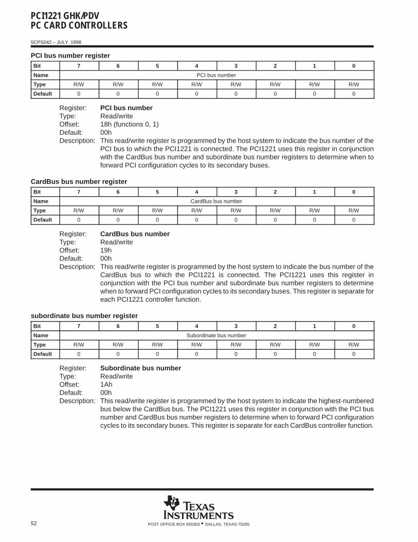
PCI1221 GHK/PDVPC CARD CONTROLLERS
SCPS042 – JULY 1998
52 POST OFFICE BOX 655303 • DALLAS, TEXAS 75265
PCI bus number registerBit 7 6 5 4 3 2 1 0
Name PCI bus number
Type R/W R/W R/W R/W R/W R/W R/W R/W
Default 0 0 0 0 0 0 0 0
Register: PCI bus numberType: Read/writeOffset: 18h (functions 0, 1)Default: 00hDescription: This read/write register is programmed by the host system to indicate the bus number of the
PCI bus to which the PCI1221 is connected. The PCI1221 uses this register in conjunctionwith the CardBus bus number and subordinate bus number registers to determine when toforward PCI configuration cycles to its secondary buses.
CardBus bus number registerBit 7 6 5 4 3 2 1 0
Name CardBus bus number
Type R/W R/W R/W R/W R/W R/W R/W R/W
Default 0 0 0 0 0 0 0 0
Register: CardBus bus numberType: Read/writeOffset: 19hDefault: 00hDescription: This read/write register is programmed by the host system to indicate the bus number of the
CardBus bus to which the PCI1221 is connected. The PCI1221 uses this register inconjunction with the PCI bus number and subordinate bus number registers to determinewhen to forward PCI configuration cycles to its secondary buses. This register is separate foreach PCI1221 controller function.
subordinate bus number registerBit 7 6 5 4 3 2 1 0
Name Subordinate bus number
Type R/W R/W R/W R/W R/W R/W R/W R/W
Default 0 0 0 0 0 0 0 0
Register: Subordinate bus numberType: Read/writeOffset: 1AhDefault: 00hDescription: This read/write register is programmed by the host system to indicate the highest-numbered
bus below the CardBus bus. The PCI1221 uses this register in conjunction with the PCI busnumber and CardBus bus number registers to determine when to forward PCI configurationcycles to its secondary buses. This register is separate for each CardBus controller function.
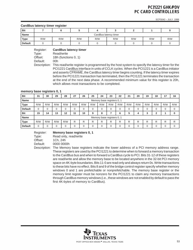
PCI1221 GHK/PDVPC CARD CONTROLLERS
SCPS042 – JULY 1998
53POST OFFICE BOX 655303 • DALLAS, TEXAS 75265
CardBus latency timer registerBit 7 6 5 4 3 2 1 0
Name CardBus latency timer
Type R/W R/W R/W R/W R/W R/W R/W R/W
Default 0 0 0 0 0 0 0 0
Register: CardBus latency timerType: Read/writeOffset: 1Bh (functions 0, 1)Default: 00hDescription: This read/write register is programmed by the host system to specify the latency timer for the
PCI1221 CardBus interface in units of CCLK cycles. When the PCI1221 is a CardBus initiatorand asserts CFRAME, the CardBus latency timer begins counting. If the latency timer expiresbefore the PCI1221 transaction has terminated, then the PCI1221 terminates the transactionat the end of the next data phase. A recommended minimum value for this register is 20h,which allows most transactions to be completed.
memory base registers 0, 1Bit 31 30 29 28 27 26 25 24 23 22 21 20 19 18 17 16
Name Memory base registers 0, 1
Type R/W R/W R/W R/W R/W R/W R/W R/W R/W R/W R/W R/W R/W R/W R/W R/W
Default 0 0 0 0 0 0 0 0 0 0 0 0 0 0 0 0
Bit 15 14 13 12 11 10 9 8 7 6 5 4 3 2 1 0
Name Memory base registers 0, 1
Type R/W R/W R/W R/W R R R R R R R R R R R R
Default 0 0 0 0 0 0 0 0 0 0 0 0 0 0 0 0
Register: Memory base registers 0, 1Type: Read only, read/writeOffset: 1Ch, 24hDefault: 0000 0000hDescription: The Memory base registers indicate the lower address of a PCI memory address range.
These registers are used by the PCI1221 to determine when to forward a memory transactionto the CardBus bus and when to forward a CardBus cycle to PCI. Bits 31-12 of these registersare read/write and allow the memory base to be located anywhere in the 32-bit PCI memoryspace on 4K-byte boundaries. Bits 11-0 are read only and always return 0s. Write transactionsto these bits have no effect. Bits 8 and 9 of the bridge control register specify whether memorywindows 0 and 1 are prefetchable or nonprefetchable. The memory base register or thememory limit register must be nonzero for the PCI1221 to claim any memory transactionsthrough CardBus memory windows (i.e., these windows are not enabled by default to pass thefirst 4K-bytes of memory to CardBus).
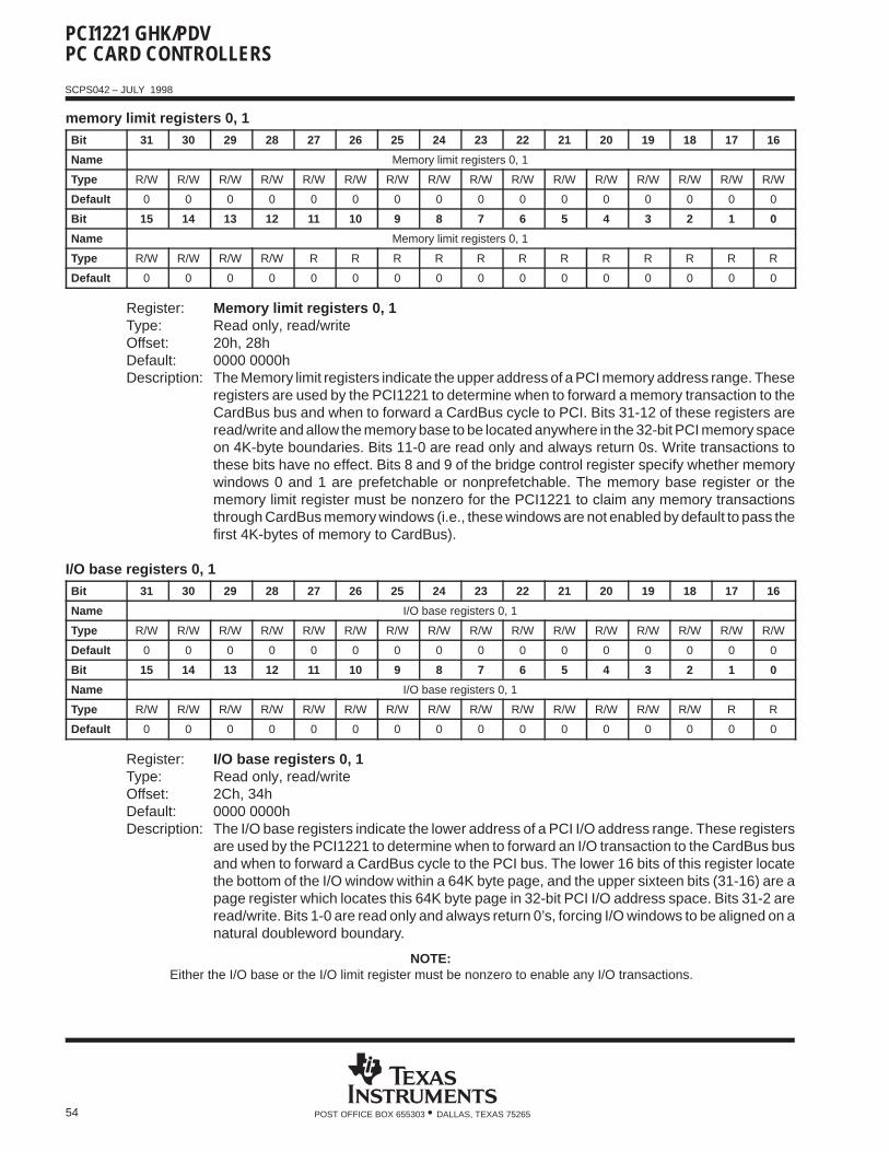
PCI1221 GHK/PDVPC CARD CONTROLLERS
SCPS042 – JULY 1998
54 POST OFFICE BOX 655303 • DALLAS, TEXAS 75265
memory limit registers 0, 1Bit 31 30 29 28 27 26 25 24 23 22 21 20 19 18 17 16
Name Memory limit registers 0, 1
Type R/W R/W R/W R/W R/W R/W R/W R/W R/W R/W R/W R/W R/W R/W R/W R/W
Default 0 0 0 0 0 0 0 0 0 0 0 0 0 0 0 0
Bit 15 14 13 12 11 10 9 8 7 6 5 4 3 2 1 0
Name Memory limit registers 0, 1
Type R/W R/W R/W R/W R R R R R R R R R R R R
Default 0 0 0 0 0 0 0 0 0 0 0 0 0 0 0 0
Register: Memory limit registers 0, 1Type: Read only, read/writeOffset: 20h, 28hDefault: 0000 0000hDescription: The Memory limit registers indicate the upper address of a PCI memory address range. These
registers are used by the PCI1221 to determine when to forward a memory transaction to theCardBus bus and when to forward a CardBus cycle to PCI. Bits 31-12 of these registers areread/write and allow the memory base to be located anywhere in the 32-bit PCI memory spaceon 4K-byte boundaries. Bits 11-0 are read only and always return 0s. Write transactions tothese bits have no effect. Bits 8 and 9 of the bridge control register specify whether memorywindows 0 and 1 are prefetchable or nonprefetchable. The memory base register or thememory limit register must be nonzero for the PCI1221 to claim any memory transactionsthrough CardBus memory windows (i.e., these windows are not enabled by default to pass thefirst 4K-bytes of memory to CardBus).
I/O base registers 0, 1Bit 31 30 29 28 27 26 25 24 23 22 21 20 19 18 17 16
Name I/O base registers 0, 1
Type R/W R/W R/W R/W R/W R/W R/W R/W R/W R/W R/W R/W R/W R/W R/W R/W
Default 0 0 0 0 0 0 0 0 0 0 0 0 0 0 0 0
Bit 15 14 13 12 11 10 9 8 7 6 5 4 3 2 1 0
Name I/O base registers 0, 1
Type R/W R/W R/W R/W R/W R/W R/W R/W R/W R/W R/W R/W R/W R/W R R
Default 0 0 0 0 0 0 0 0 0 0 0 0 0 0 0 0
Register: I/O base registers 0, 1Type: Read only, read/writeOffset: 2Ch, 34hDefault: 0000 0000hDescription: The I/O base registers indicate the lower address of a PCI I/O address range. These registers
are used by the PCI1221 to determine when to forward an I/O transaction to the CardBus busand when to forward a CardBus cycle to the PCI bus. The lower 16 bits of this register locatethe bottom of the I/O window within a 64K byte page, and the upper sixteen bits (31-16) are apage register which locates this 64K byte page in 32-bit PCI I/O address space. Bits 31-2 areread/write. Bits 1-0 are read only and always return 0’s, forcing I/O windows to be aligned on anatural doubleword boundary.
NOTE:Either the I/O base or the I/O limit register must be nonzero to enable any I/O transactions.
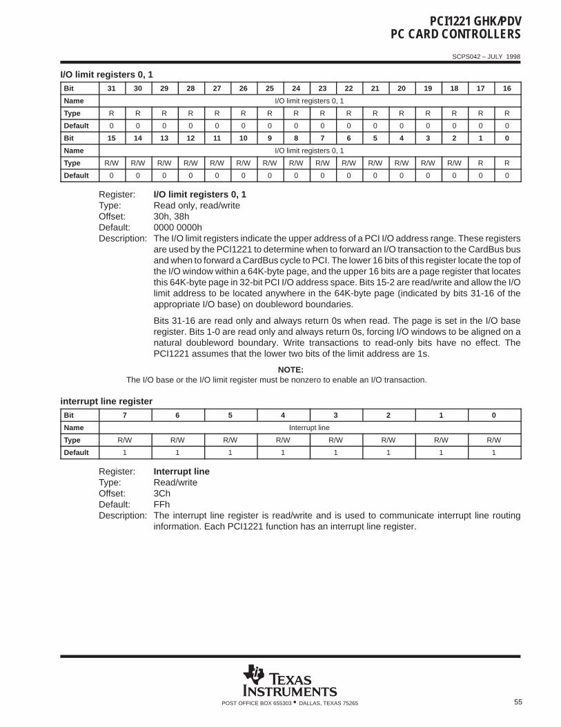
PCI1221 GHK/PDVPC CARD CONTROLLERS
SCPS042 – JULY 1998
55POST OFFICE BOX 655303 • DALLAS, TEXAS 75265
I/O limit registers 0, 1Bit 31 30 29 28 27 26 25 24 23 22 21 20 19 18 17 16
Name I/O limit registers 0, 1
Type R R R R R R R R R R R R R R R R
Default 0 0 0 0 0 0 0 0 0 0 0 0 0 0 0 0
Bit 15 14 13 12 11 10 9 8 7 6 5 4 3 2 1 0
Name I/O limit registers 0, 1
Type R/W R/W R/W R/W R/W R/W R/W R/W R/W R/W R/W R/W R/W R/W R R
Default 0 0 0 0 0 0 0 0 0 0 0 0 0 0 0 0
Register: I/O limit registers 0, 1Type: Read only, read/writeOffset: 30h, 38hDefault: 0000 0000hDescription: The I/O limit registers indicate the upper address of a PCI I/O address range. These registers
are used by the PCI1221 to determine when to forward an I/O transaction to the CardBus busand when to forward a CardBus cycle to PCI. The lower 16 bits of this register locate the top ofthe I/O window within a 64K-byte page, and the upper 16 bits are a page register that locatesthis 64K-byte page in 32-bit PCI I/O address space. Bits 15-2 are read/write and allow the I/Olimit address to be located anywhere in the 64K-byte page (indicated by bits 31-16 of theappropriate I/O base) on doubleword boundaries.
Bits 31-16 are read only and always return 0s when read. The page is set in the I/O baseregister. Bits 1-0 are read only and always return 0s, forcing I/O windows to be aligned on anatural doubleword boundary. Write transactions to read-only bits have no effect. ThePCI1221 assumes that the lower two bits of the limit address are 1s.
NOTE:The I/O base or the I/O limit register must be nonzero to enable an I/O transaction.
interrupt line registerBit 7 6 5 4 3 2 1 0
Name Interrupt line
Type R/W R/W R/W R/W R/W R/W R/W R/W
Default 1 1 1 1 1 1 1 1
Register: Interrupt lineType: Read/writeOffset: 3ChDefault: FFhDescription: The interrupt line register is read/write and is used to communicate interrupt line routing
information. Each PCI1221 function has an interrupt line register.
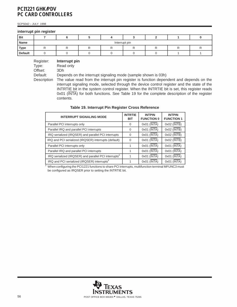
PCI1221 GHK/PDVPC CARD CONTROLLERS
SCPS042 – JULY 1998
56 POST OFFICE BOX 655303 • DALLAS, TEXAS 75265
interrupt pin registerBit 7 6 5 4 3 2 1 0
Name Interrupt pin
Type R R R R R R R R
Default 0 0 0 0 0 0 1 1
Register: Interrupt pinType: Read onlyOffset: 3DhDefault: Depends on the interrupt signaling mode (sample shown is 03h)Description The value read from the interrupt pin register is function dependent and depends on the
interrupt signaling mode, selected through the device control register and the state of theINTRTIE bit in the system control register. When the INTRTIE bit is set, this register reads0x01 (INTA) for both functions. See Table 19 for the complete description of the registercontents.
Table 19. Interrupt Pin Register Cross Reference
INTERRUPT SIGNALING MODEINTRTIE
BITINTPIN
FUNCTION 0INTPIN
FUNCTION 1
Parallel PCI interrupts only 0 0x01 (INTA) 0x02 (INTB)
Parallel IRQ and parallel PCI interrupts 0 0x01 (INTA) 0x02 (INTB)
IRQ serialized (IRQSER) and parallel PCI interrupts 0 0x01 (INTA) 0x02 (INTB)
IRQ and PCI serialized (IRQSER) interrupts (default) 0 0x01 (INTA) 0x02 (INTB)
Parallel PCI interrupts only 1 0x01 (INTA) 0x01 (INTA)
Parallel IRQ and parallel PCI interrupts 1 0x01 (INTA) 0x01 (INTA)
IRQ serialized (IRQSER) and parallel PCI interrupts† 1 0x01 (INTA) 0x01 (INTA)
IRQ and PCI serialized (IRQSER) interrupts† 1 0x01 (INTA) 0x01 (INTA)† When configuring the PCI1221 functions to share PCI interrupts, multifunction terminal MFUNC3 must
be configured as IRQSER prior to setting the INTRTIE bit.
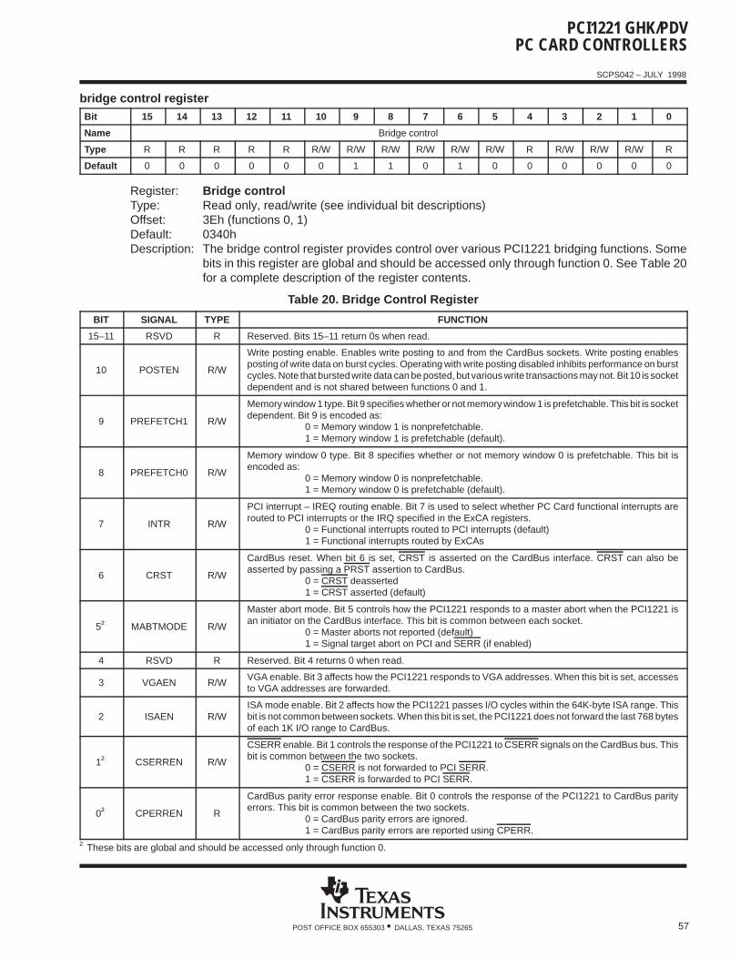
PCI1221 GHK/PDVPC CARD CONTROLLERS
SCPS042 – JULY 1998
57POST OFFICE BOX 655303 • DALLAS, TEXAS 75265
bridge control registerBit 15 14 13 12 11 10 9 8 7 6 5 4 3 2 1 0
Name Bridge control
Type R R R R R R/W R/W R/W R/W R/W R/W R R/W R/W R/W R
Default 0 0 0 0 0 0 1 1 0 1 0 0 0 0 0 0
Register: Bridge controlType: Read only, read/write (see individual bit descriptions)Offset: 3Eh (functions 0, 1)Default: 0340hDescription: The bridge control register provides control over various PCI1221 bridging functions. Some
bits in this register are global and should be accessed only through function 0. See Table 20for a complete description of the register contents.
Table 20. Bridge Control Register
BIT SIGNAL TYPE FUNCTION
15–11 RSVD R Reserved. Bits 15–11 return 0s when read.
10 POSTEN R/W
Write posting enable. Enables write posting to and from the CardBus sockets. Write posting enablesposting of write data on burst cycles. Operating with write posting disabled inhibits performance on burstcycles. Note that bursted write data can be posted, but various write transactions may not. Bit 10 is socketdependent and is not shared between functions 0 and 1.
9 PREFETCH1 R/W
Memory window 1 type. Bit 9 specifies whether or not memory window 1 is prefetchable. This bit is socketdependent. Bit 9 is encoded as:
0 = Memory window 1 is nonprefetchable.1 = Memory window 1 is prefetchable (default).
8 PREFETCH0 R/W
Memory window 0 type. Bit 8 specifies whether or not memory window 0 is prefetchable. This bit isencoded as:
0 = Memory window 0 is nonprefetchable.1 = Memory window 0 is prefetchable (default).
7 INTR R/W
PCI interrupt – IREQ routing enable. Bit 7 is used to select whether PC Card functional interrupts arerouted to PCI interrupts or the IRQ specified in the ExCA registers.
0 = Functional interrupts routed to PCI interrupts (default)1 = Functional interrupts routed by ExCAs
6 CRST R/W
CardBus reset. When bit 6 is set, CRST is asserted on the CardBus interface. CRST can also beasserted by passing a PRST assertion to CardBus.
0 = CRST deasserted1 = CRST asserted (default)
5† MABTMODE R/W
Master abort mode. Bit 5 controls how the PCI1221 responds to a master abort when the PCI1221 isan initiator on the CardBus interface. This bit is common between each socket.
0 = Master aborts not reported (default)1 = Signal target abort on PCI and SERR (if enabled)
4 RSVD R Reserved. Bit 4 returns 0 when read.
3 VGAEN R/WVGA enable. Bit 3 affects how the PCI1221 responds to VGA addresses. When this bit is set, accessesto VGA addresses are forwarded.
2 ISAEN R/WISA mode enable. Bit 2 affects how the PCI1221 passes I/O cycles within the 64K-byte ISA range. Thisbit is not common between sockets. When this bit is set, the PCI1221 does not forward the last 768 bytesof each 1K I/O range to CardBus.
1† CSERREN R/W
CSERR enable. Bit 1 controls the response of the PCI1221 to CSERR signals on the CardBus bus. Thisbit is common between the two sockets.
0 = CSERR is not forwarded to PCI SERR.1 = CSERR is forwarded to PCI SERR.
0† CPERREN R
CardBus parity error response enable. Bit 0 controls the response of the PCI1221 to CardBus parityerrors. This bit is common between the two sockets.
0 = CardBus parity errors are ignored.1 = CardBus parity errors are reported using CPERR.
† These bits are global and should be accessed only through function 0.
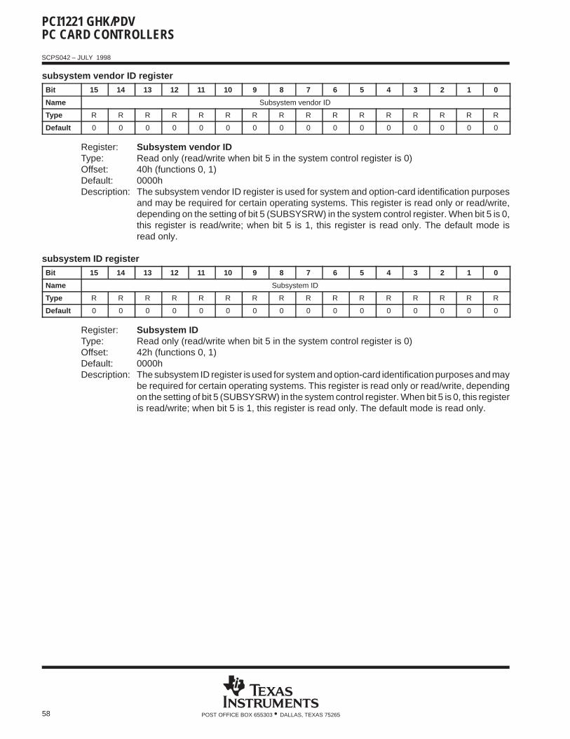
PCI1221 GHK/PDVPC CARD CONTROLLERS
SCPS042 – JULY 1998
58 POST OFFICE BOX 655303 • DALLAS, TEXAS 75265
subsystem vendor ID registerBit 15 14 13 12 11 10 9 8 7 6 5 4 3 2 1 0
Name Subsystem vendor ID
Type R R R R R R R R R R R R R R R R
Default 0 0 0 0 0 0 0 0 0 0 0 0 0 0 0 0
Register: Subsystem vendor IDType: Read only (read/write when bit 5 in the system control register is 0)Offset: 40h (functions 0, 1)Default: 0000hDescription: The subsystem vendor ID register is used for system and option-card identification purposes
and may be required for certain operating systems. This register is read only or read/write,depending on the setting of bit 5 (SUBSYSRW) in the system control register. When bit 5 is 0,this register is read/write; when bit 5 is 1, this register is read only. The default mode isread only.
subsystem ID registerBit 15 14 13 12 11 10 9 8 7 6 5 4 3 2 1 0
Name Subsystem ID
Type R R R R R R R R R R R R R R R R
Default 0 0 0 0 0 0 0 0 0 0 0 0 0 0 0 0
Register: Subsystem IDType: Read only (read/write when bit 5 in the system control register is 0)Offset: 42h (functions 0, 1)Default: 0000hDescription: The subsystem ID register is used for system and option-card identification purposes and may
be required for certain operating systems. This register is read only or read/write, dependingon the setting of bit 5 (SUBSYSRW) in the system control register. When bit 5 is 0, this registeris read/write; when bit 5 is 1, this register is read only. The default mode is read only.
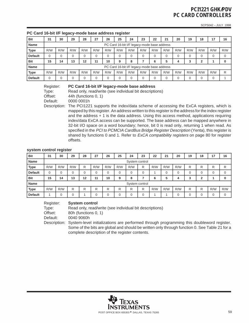
PCI1221 GHK/PDVPC CARD CONTROLLERS
SCPS042 – JULY 1998
59POST OFFICE BOX 655303 • DALLAS, TEXAS 75265
PC Card 16-bit I/F legacy-mode base address registerBit 31 30 29 28 27 26 25 24 23 22 21 20 19 18 17 16
Name PC Card 16-bit I/F legacy-mode base address
Type R/W R/W R/W R/W R/W R/W R/W R/W R/W R/W R/W R/W R/W R/W R/W R/W
Default 0 0 0 0 0 0 0 0 0 0 0 0 0 0 0 0
Bit 15 14 13 12 11 10 9 8 7 6 5 4 3 2 1 0
Name PC Card 16-bit I/F legacy-mode base address
Type R/W R/W R/W R/W R/W R/W R/W R/W R/W R/W R/W R/W R/W R/W R/W R
Default 0 0 0 0 0 0 0 0 0 0 0 0 0 0 0 1
Register: PC Card 16-bit I/F legacy-mode base addressType: Read only, read/write (see individual bit descriptions)Offset: 44h (functions 0, 1)Default: 0000 0001hDescription: The PCI1221 supports the index/data scheme of accessing the ExCA registers, which is
mapped by this register. An address written to this register is the address for the index registerand the address + 1 is the data address. Using this access method, applications requiringindex/data ExCA access can be supported. The base address can be mapped anywhere in32-bit I/O space on a word boundary; hence, bit 0 is read only, returning 1 when read. Asspecified in the PCI to PCMCIA CardBus Bridge Register Description (Yenta), this register isshared by functions 0 and 1. Refer to ExCA compatibility registers on page 80 for registeroffsets.
system control registerBit 31 30 29 28 27 26 25 24 23 22 21 20 19 18 17 16
Name System control
Type R/W R/W R/W R R/W R/W R/W R/W R R/W R/W R/W R R R R
Default 0 0 0 0 0 0 0 0 0 1 0 0 0 0 0 0
Bit 15 14 13 12 11 10 9 8 7 6 5 4 3 2 1 0
Name System control
Type R/W R/W R R R R R R R R/W R/W R/W R R R/W R/W
Default 1 0 0 1 0 0 0 0 0 1 1 0 0 0 0 0
Register: System controlType: Read only, read/write (see individual bit descriptions)Offset: 80h (functions 0, 1)Default: 0040 9060hDescription: System-level initializations are performed through programming this doubleword register.
Some of the bits are global and should be written only through function 0. See Table 21 for acomplete description of the register contents.
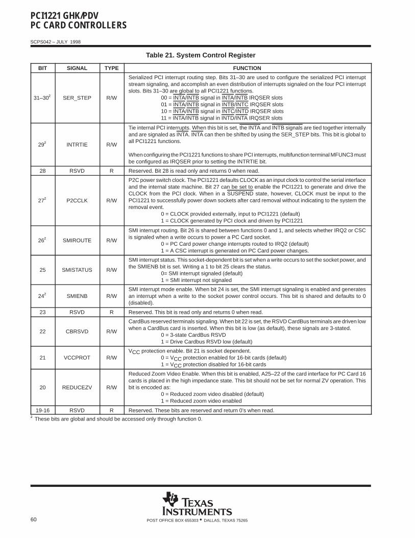
PCI1221 GHK/PDVPC CARD CONTROLLERS
SCPS042 – JULY 1998
60 POST OFFICE BOX 655303 • DALLAS, TEXAS 75265
Table 21. System Control Register
BIT SIGNAL TYPE FUNCTION
31–30† SER_STEP R/W
Serialized PCI interrupt routing step. Bits 31–30 are used to configure the serialized PCI interruptstream signaling, and accomplish an even distribution of interrupts signaled on the four PCI interruptslots. Bits 31–30 are global to all PCI1221 functions.
00 = INTA/INTB signal in INTA/INTB IRQSER slots01 = INTA/INTB signal in INTB/INTC IRQSER slots10 = INTA/INTB signal in INTC/INTD IRQSER slots11 = INTA/INTB signal in INTD/INTA IRQSER slots
29† INTRTIE R/W
Tie internal PCI interrupts. When this bit is set, the INTA and INTB signals are tied together internallyand are signaled as INTA. INTA can then be shifted by using the SER_STEP bits. This bit is global toall PCI1221 functions.
When configuring the PCI1221 functions to share PCI interrupts, multifunction terminal MFUNC3 mustbe configured as IRQSER prior to setting the INTRTIE bit.
28 RSVD R Reserved. Bit 28 is read only and returns 0 when read.
27† P2CCLK R/W
P2C power switch clock. The PCI1221 defaults CLOCK as an input clock to control the serial interfaceand the internal state machine. Bit 27 can be set to enable the PCI1221 to generate and drive theCLOCK from the PCI clock. When in a SUSPEND state, however, CLOCK must be input to thePCI1221 to successfully power down sockets after card removal without indicating to the system theremoval event.
0 = CLOCK provided externally, input to PCI1221 (default)1 = CLOCK generated by PCI clock and driven by PCI1221
26† SMIROUTE R/W
SMI interrupt routing. Bit 26 is shared between functions 0 and 1, and selects whether IRQ2 or CSCis signaled when a write occurs to power a PC Card socket.
0 = PC Card power change interrupts routed to IRQ2 (default)1 = A CSC interrupt is generated on PC Card power changes.
25 SMISTATUS R/W
SMI interrupt status. This socket-dependent bit is set when a write occurs to set the socket power, andthe SMIENB bit is set. Writing a 1 to bit 25 clears the status.
0= SMI interrupt signaled (default)1 = SMI interrupt not signaled
24† SMIENB R/WSMI interrupt mode enable. When bit 24 is set, the SMI interrupt signaling is enabled and generatesan interrupt when a write to the socket power control occurs. This bit is shared and defaults to 0(disabled).
23 RSVD R Reserved. This bit is read only and returns 0 when read.
22 CBRSVD R/W
CardBus reserved terminals signaling. When bit 22 is set, the RSVD CardBus terminals are driven lowwhen a CardBus card is inserted. When this bit is low (as default), these signals are 3-stated.
0 = 3-state CardBus RSVD1 = Drive Cardbus RSVD low (default)
21 VCCPROT R/WVCC protection enable. Bit 21 is socket dependent.
0 = VCC protection enabled for 16-bit cards (default)1 = VCC protection disabled for 16-bit cards
20 REDUCEZV R/W
Reduced Zoom Video Enable. When this bit is enabled, A25–22 of the card interface for PC Card 16cards is placed in the high impedance state. This bit should not be set for normal ZV operation. Thisbit is encoded as:
0 = Reduced zoom video disabled (default)1 = Reduced zoom video enabled
19-16 RSVD R Reserved. These bits are reserved and return 0’s when read.† These bits are global and should be accessed only through function 0.
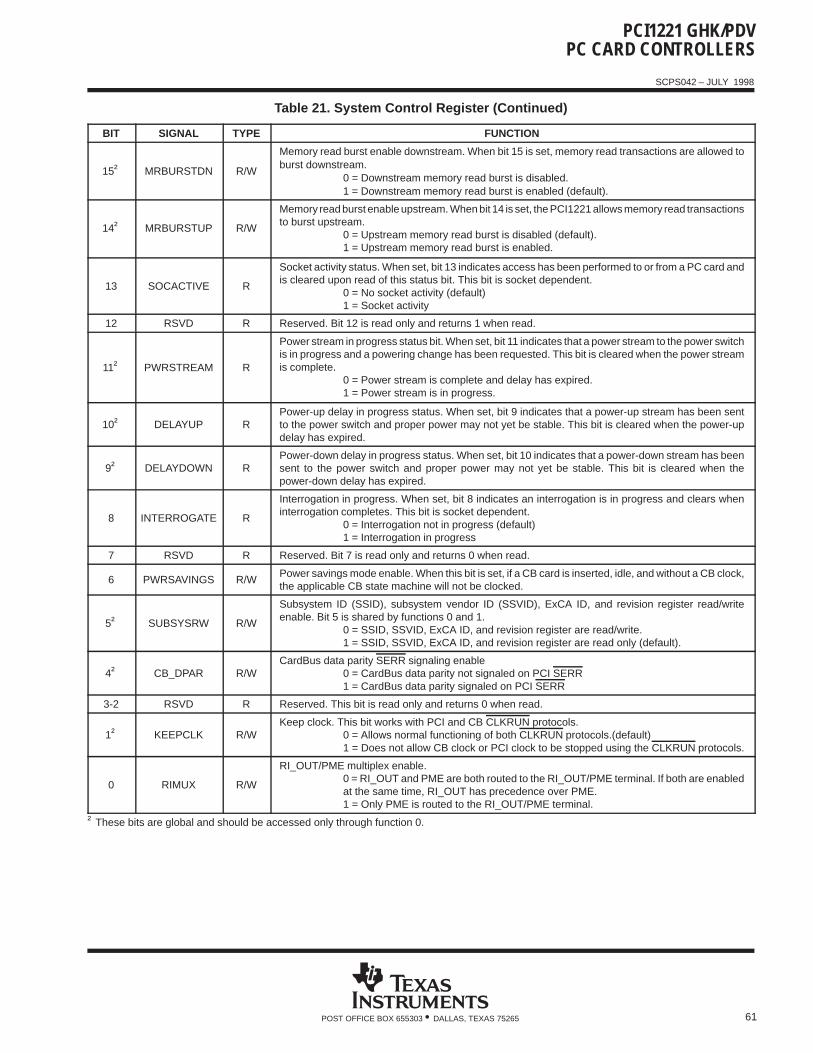
PCI1221 GHK/PDVPC CARD CONTROLLERS
SCPS042 – JULY 1998
61POST OFFICE BOX 655303 • DALLAS, TEXAS 75265
Table 21. System Control Register (Continued)
BIT SIGNAL TYPE FUNCTION
15† MRBURSTDN R/W
Memory read burst enable downstream. When bit 15 is set, memory read transactions are allowed toburst downstream.
0 = Downstream memory read burst is disabled.1 = Downstream memory read burst is enabled (default).
14† MRBURSTUP R/W
Memory read burst enable upstream. When bit 14 is set, the PCI1221 allows memory read transactionsto burst upstream.
0 = Upstream memory read burst is disabled (default).1 = Upstream memory read burst is enabled.
13 SOCACTIVE R
Socket activity status. When set, bit 13 indicates access has been performed to or from a PC card andis cleared upon read of this status bit. This bit is socket dependent.
0 = No socket activity (default)1 = Socket activity
12 RSVD R Reserved. Bit 12 is read only and returns 1 when read.
11† PWRSTREAM R
Power stream in progress status bit. When set, bit 11 indicates that a power stream to the power switchis in progress and a powering change has been requested. This bit is cleared when the power streamis complete.
0 = Power stream is complete and delay has expired.1 = Power stream is in progress.
10† DELAYUP RPower-up delay in progress status. When set, bit 9 indicates that a power-up stream has been sentto the power switch and proper power may not yet be stable. This bit is cleared when the power-updelay has expired.
9† DELAYDOWN RPower-down delay in progress status. When set, bit 10 indicates that a power-down stream has beensent to the power switch and proper power may not yet be stable. This bit is cleared when thepower-down delay has expired.
8 INTERROGATE R
Interrogation in progress. When set, bit 8 indicates an interrogation is in progress and clears wheninterrogation completes. This bit is socket dependent.
0 = Interrogation not in progress (default)1 = Interrogation in progress
7 RSVD R Reserved. Bit 7 is read only and returns 0 when read.
6 PWRSAVINGS R/WPower savings mode enable. When this bit is set, if a CB card is inserted, idle, and without a CB clock,the applicable CB state machine will not be clocked.
5† SUBSYSRW R/W
Subsystem ID (SSID), subsystem vendor ID (SSVID), ExCA ID, and revision register read/writeenable. Bit 5 is shared by functions 0 and 1.
0 = SSID, SSVID, ExCA ID, and revision register are read/write.1 = SSID, SSVID, ExCA ID, and revision register are read only (default).
4† CB_DPAR R/WCardBus data parity SERR signaling enable
0 = CardBus data parity not signaled on PCI SERR1 = CardBus data parity signaled on PCI SERR
3-2 RSVD R Reserved. This bit is read only and returns 0 when read.
1† KEEPCLK R/WKeep clock. This bit works with PCI and CB CLKRUN protocols.
0 = Allows normal functioning of both CLKRUN protocols.(default)1 = Does not allow CB clock or PCI clock to be stopped using the CLKRUN protocols.
0 RIMUX R/W
RI_OUT/PME multiplex enable.0 = RI_OUT and PME are both routed to the RI_OUT/PME terminal. If both are enabledat the same time, RI_OUT has precedence over PME.1 = Only PME is routed to the RI_OUT/PME terminal.
† These bits are global and should be accessed only through function 0.
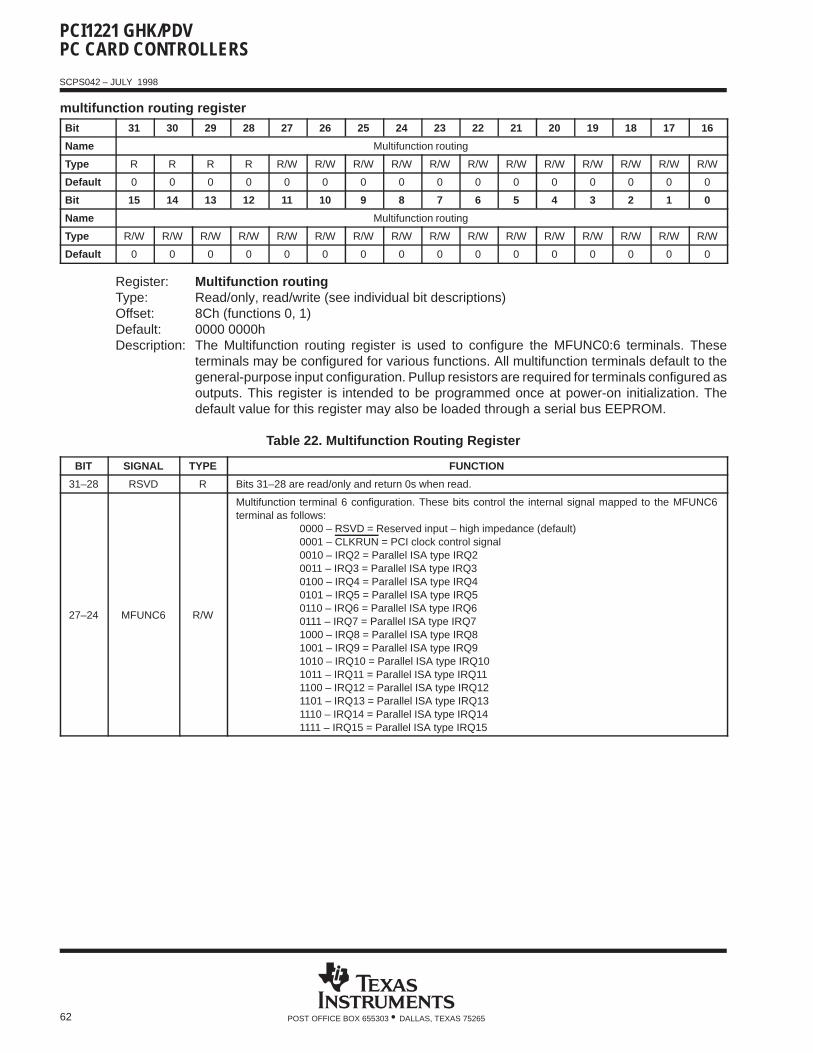
PCI1221 GHK/PDVPC CARD CONTROLLERS
SCPS042 – JULY 1998
62 POST OFFICE BOX 655303 • DALLAS, TEXAS 75265
multifunction routing registerBit 31 30 29 28 27 26 25 24 23 22 21 20 19 18 17 16
Name Multifunction routing
Type R R R R R/W R/W R/W R/W R/W R/W R/W R/W R/W R/W R/W R/W
Default 0 0 0 0 0 0 0 0 0 0 0 0 0 0 0 0
Bit 15 14 13 12 11 10 9 8 7 6 5 4 3 2 1 0
Name Multifunction routing
Type R/W R/W R/W R/W R/W R/W R/W R/W R/W R/W R/W R/W R/W R/W R/W R/W
Default 0 0 0 0 0 0 0 0 0 0 0 0 0 0 0 0
Register: Multifunction routingType: Read/only, read/write (see individual bit descriptions)Offset: 8Ch (functions 0, 1)Default: 0000 0000hDescription: The Multifunction routing register is used to configure the MFUNC0:6 terminals. These
terminals may be configured for various functions. All multifunction terminals default to thegeneral-purpose input configuration. Pullup resistors are required for terminals configured asoutputs. This register is intended to be programmed once at power-on initialization. Thedefault value for this register may also be loaded through a serial bus EEPROM.
Table 22. Multifunction Routing Register
BIT SIGNAL TYPE FUNCTION
31–28 RSVD R Bits 31–28 are read/only and return 0s when read.
27–24 MFUNC6 R/W
Multifunction terminal 6 configuration. These bits control the internal signal mapped to the MFUNC6terminal as follows:
0000 – RSVD = Reserved input – high impedance (default)0001 – CLKRUN = PCI clock control signal0010 – IRQ2 = Parallel ISA type IRQ20011 – IRQ3 = Parallel ISA type IRQ30100 – IRQ4 = Parallel ISA type IRQ40101 – IRQ5 = Parallel ISA type IRQ50110 – IRQ6 = Parallel ISA type IRQ60111 – IRQ7 = Parallel ISA type IRQ71000 – IRQ8 = Parallel ISA type IRQ81001 – IRQ9 = Parallel ISA type IRQ91010 – IRQ10 = Parallel ISA type IRQ101011 – IRQ11 = Parallel ISA type IRQ111100 – IRQ12 = Parallel ISA type IRQ121101 – IRQ13 = Parallel ISA type IRQ131110 – IRQ14 = Parallel ISA type IRQ141111 – IRQ15 = Parallel ISA type IRQ15
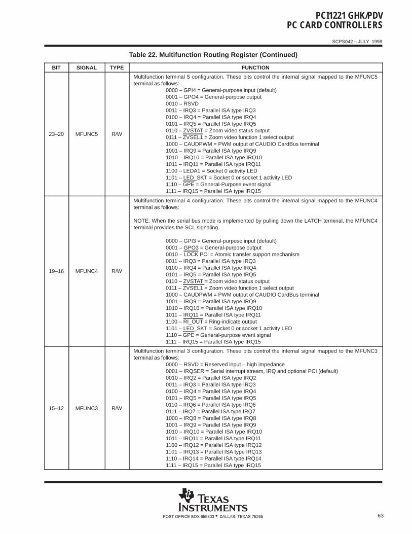
PCI1221 GHK/PDVPC CARD CONTROLLERS
SCPS042 – JULY 1998
63POST OFFICE BOX 655303 • DALLAS, TEXAS 75265
Table 22. Multifunction Routing Register (Continued)
BIT SIGNAL TYPE FUNCTION
23–20 MFUNC5 R/W
Multifunction terminal 5 configuration. These bits control the internal signal mapped to the MFUNC5terminal as follows:
0000 – GPI4 = General-purpose input (default)0001 – GPO4 = General-purpose output0010 – RSVD0011 – IRQ3 = Parallel ISA type IRQ30100 – IRQ4 = Parallel ISA type IRQ40101 – IRQ5 = Parallel ISA type IRQ50110 – ZVSTAT = Zoom video status output0111 – ZVSEL1 = Zoom video function 1 select output1000 – CAUDPWM = PWM output of CAUDIO CardBus terminal1001 – IRQ9 = Parallel ISA type IRQ91010 – IRQ10 = Parallel ISA type IRQ101011 – IRQ11 = Parallel ISA type IRQ111100 – LEDA1 = Socket 0 activity LED1101 – LED_SKT = Socket 0 or socket 1 activity LED1110 – GPE = General-Purpose event signal1111 – IRQ15 = Parallel ISA type IRQ15
19–16 MFUNC4 R/W
Multifunction terminal 4 configuration. These bits control the internal signal mapped to the MFUNC4terminal as follows:
NOTE: When the serial bus mode is implemented by pulling down the LATCH terminal, the MFUNC4terminal provides the SCL signaling.
0000 – GPI3 = General-purpose input (default)0001 – GPO3 = General-purpose output0010 – LOCK PCI = Atomic transfer support mechanism0011 – IRQ3 = Parallel ISA type IRQ30100 – IRQ4 = Parallel ISA type IRQ40101 – IRQ5 = Parallel ISA type IRQ50110 – ZVSTAT = Zoom video status output0111 – ZVSEL1 = Zoom video function 1 select output1000 – CAUDPWM = PWM output of CAUDIO CardBus terminal1001 – IRQ9 = Parallel ISA type IRQ91010 – IRQ10 = Parallel ISA type IRQ101011 – IRQ11 = Parallel ISA type IRQ111100 – RI_OUT = Ring-indicate output1101 – LED_SKT = Socket 0 or socket 1 activity LED1110 – GPE = General-purpose event signal1111 – IRQ15 = Parallel ISA type IRQ15
15–12 MFUNC3 R/W
Multifunction terminal 3 configuration. These bits control the internal signal mapped to the MFUNC3terminal as follows:
0000 – RSVD = Reserved input – high impedance 0001 – IRQSER = Serial interrupt stream, IRQ and optional PCI (default)0010 – IRQ2 = Parallel ISA type IRQ20011 – IRQ3 = Parallel ISA type IRQ30100 – IRQ4 = Parallel ISA type IRQ40101 – IRQ5 = Parallel ISA type IRQ50110 – IRQ6 = Parallel ISA type IRQ60111 – IRQ7 = Parallel ISA type IRQ71000 – IRQ8 = Parallel ISA type IRQ81001 – IRQ9 = Parallel ISA type IRQ91010 – IRQ10 = Parallel ISA type IRQ101011 – IRQ11 = Parallel ISA type IRQ111100 – IRQ12 = Parallel ISA type IRQ121101 – IRQ13 = Parallel ISA type IRQ131110 – IRQ14 = Parallel ISA type IRQ141111 – IRQ15 = Parallel ISA type IRQ15
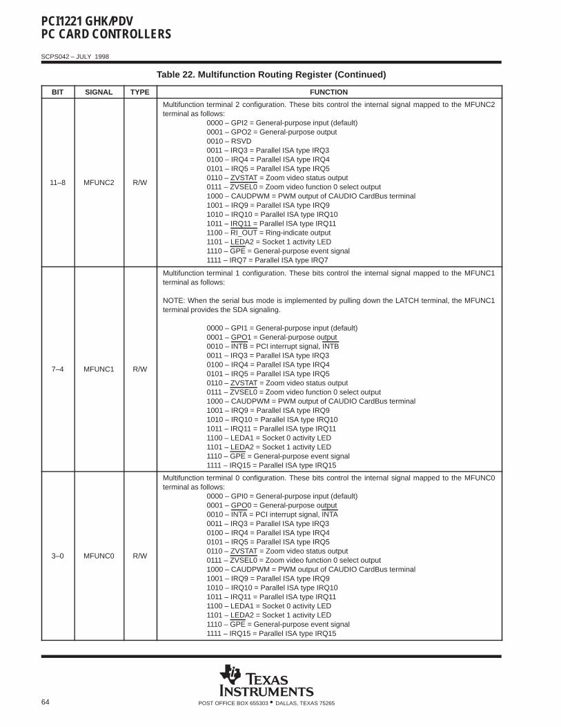
PCI1221 GHK/PDVPC CARD CONTROLLERS
SCPS042 – JULY 1998
64 POST OFFICE BOX 655303 • DALLAS, TEXAS 75265
Table 22. Multifunction Routing Register (Continued)
BIT SIGNAL TYPE FUNCTION
11–8 MFUNC2 R/W
Multifunction terminal 2 configuration. These bits control the internal signal mapped to the MFUNC2terminal as follows:
0000 – GPI2 = General-purpose input (default)0001 – GPO2 = General-purpose output0010 – RSVD0011 – IRQ3 = Parallel ISA type IRQ30100 – IRQ4 = Parallel ISA type IRQ40101 – IRQ5 = Parallel ISA type IRQ50110 – ZVSTAT = Zoom video status output0111 – ZVSEL0 = Zoom video function 0 select output1000 – CAUDPWM = PWM output of CAUDIO CardBus terminal1001 – IRQ9 = Parallel ISA type IRQ91010 – IRQ10 = Parallel ISA type IRQ101011 – IRQ11 = Parallel ISA type IRQ111100 – RI_OUT = Ring-indicate output1101 – LEDA2 = Socket 1 activity LED1110 – GPE = General-purpose event signal1111 – IRQ7 = Parallel ISA type IRQ7
7–4 MFUNC1 R/W
Multifunction terminal 1 configuration. These bits control the internal signal mapped to the MFUNC1terminal as follows:
NOTE: When the serial bus mode is implemented by pulling down the LATCH terminal, the MFUNC1terminal provides the SDA signaling.
0000 – GPI1 = General-purpose input (default)0001 – GPO1 = General-purpose output0010 – INTB = PCI interrupt signal, INTB0011 – IRQ3 = Parallel ISA type IRQ30100 – IRQ4 = Parallel ISA type IRQ40101 – IRQ5 = Parallel ISA type IRQ50110 – ZVSTAT = Zoom video status output0111 – ZVSEL0 = Zoom video function 0 select output1000 – CAUDPWM = PWM output of CAUDIO CardBus terminal1001 – IRQ9 = Parallel ISA type IRQ91010 – IRQ10 = Parallel ISA type IRQ101011 – IRQ11 = Parallel ISA type IRQ111100 – LEDA1 = Socket 0 activity LED1101 – LEDA2 = Socket 1 activity LED1110 – GPE = General-purpose event signal1111 – IRQ15 = Parallel ISA type IRQ15
3–0 MFUNC0 R/W
Multifunction terminal 0 configuration. These bits control the internal signal mapped to the MFUNC0terminal as follows:
0000 – GPI0 = General-purpose input (default)0001 – GPO0 = General-purpose output0010 – INTA = PCI interrupt signal, INTA0011 – IRQ3 = Parallel ISA type IRQ30100 – IRQ4 = Parallel ISA type IRQ40101 – IRQ5 = Parallel ISA type IRQ50110 – ZVSTAT = Zoom video status output0111 – ZVSEL0 = Zoom video function 0 select output1000 – CAUDPWM = PWM output of CAUDIO CardBus terminal1001 – IRQ9 = Parallel ISA type IRQ91010 – IRQ10 = Parallel ISA type IRQ101011 – IRQ11 = Parallel ISA type IRQ111100 – LEDA1 = Socket 0 activity LED1101 – LEDA2 = Socket 1 activity LED1110 – GPE = General-purpose event signal1111 – IRQ15 = Parallel ISA type IRQ15
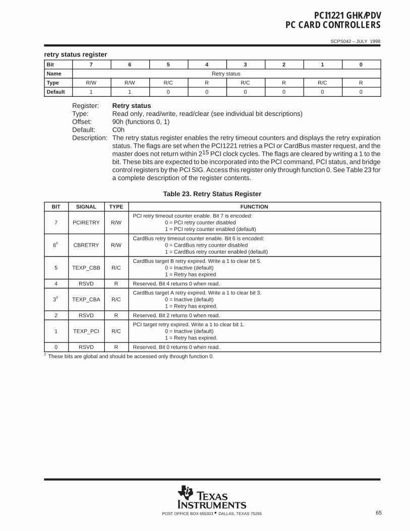
PCI1221 GHK/PDVPC CARD CONTROLLERS
SCPS042 – JULY 1998
65POST OFFICE BOX 655303 • DALLAS, TEXAS 75265
retry status registerBit 7 6 5 4 3 2 1 0
Name Retry status
Type R/W R/W R/C R R/C R R/C R
Default 1 1 0 0 0 0 0 0
Register: Retry statusType: Read only, read/write, read/clear (see individual bit descriptions)Offset: 90h (functions 0, 1)Default: C0hDescription: The retry status register enables the retry timeout counters and displays the retry expiration
status. The flags are set when the PCI1221 retries a PCI or CardBus master request, and themaster does not return within 215 PCI clock cycles. The flags are cleared by writing a 1 to thebit. These bits are expected to be incorporated into the PCI command, PCI status, and bridgecontrol registers by the PCI SIG. Access this register only through function 0. See Table 23 fora complete description of the register contents.
Table 23. Retry Status Register
BIT SIGNAL TYPE FUNCTION
7 PCIRETRY R/WPCI retry timeout counter enable. Bit 7 is encoded:
0 = PCI retry counter disabled1 = PCI retry counter enabled (default)
6† CBRETRY R/WCardBus retry timeout counter enable. Bit 6 is encoded:
0 = CardBus retry counter disabled1 = CardBus retry counter enabled (default)
5 TEXP_CBB R/CCardBus target B retry expired. Write a 1 to clear bit 5.
0 = Inactive (default)1 = Retry has expired
4 RSVD R Reserved. Bit 4 returns 0 when read.
3† TEXP_CBA R/CCardBus target A retry expired. Write a 1 to clear bit 3.
0 = Inactive (default)1 = Retry has expired.
2 RSVD R Reserved. Bit 2 returns 0 when read.
1 TEXP_PCI R/CPCI target retry expired. Write a 1 to clear bit 1.
0 = Inactive (default)1 = Retry has expired.
0 RSVD R Reserved. Bit 0 returns 0 when read.
† These bits are global and should be accessed only through function 0.
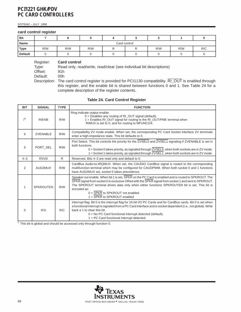
PCI1221 GHK/PDVPC CARD CONTROLLERS
SCPS042 – JULY 1998
66 POST OFFICE BOX 655303 • DALLAS, TEXAS 75265
card control registerBit 7 6 5 4 3 2 1 0
Name Card control
Type R/W R/W R/W R R R/W R/W R/C
Default 0 0 0 0 0 0 0 0
Register: Card controlType: Read only, read/write, read/clear (see individual bit descriptions)Offset: 91hDefault: 00hDescription: The card control register is provided for PCI1130 compatibility. RI_OUT is enabled through
this register, and the enable bit is shared between functions 0 and 1. See Table 24 for acomplete description of the register contents.
Table 24. Card Control Register
BIT SIGNAL TYPE FUNCTION
7† RIENB R/W
Ring indicate output enable.0 = Disables any routing of RI_OUT signal (default).1 = Enables RI_OUT signal for routing to the RI_OUT/PME terminal when RIMUX is set to 0, and for routing to MFUNC2/4.
6 ZVENABLE R/WCompatibility ZV mode enable. When set, the corresponding PC Card Socket interface ZV terminalsenter a high-impedance state. This bit defaults to 0.
5 PORT_SEL R/W
Port Select. This bit controls the priority for the ZVSEL0 and ZVSEL1 signaling if ZVENABLE is set inboth functions.
0 = Socket 0 takes priority, as signaled through ZVSEL0, when both sockets are in ZV mode.1 = Socket 1 takes priority, as signaled through ZVSEL1, when both sockets are in ZV mode.
4–3 RSVD R Reserved. Bits 4–3 are read only and default to 0.
2 AUD2MUX R/WCardBus Audio-to-IRQMUX. When set, the CAUDIO CardBus signal is routed to the correspondingmultifunction terminal which may be configured for CAUDPWM. When both socket 0 and 1 functionshave AUD2MUX set, socket 0 takes precedence.
1 SPKROUTEN R/W
Speaker out enable. When bit 1 is set, SPKR on the PC Card is enabled and is routed to SPKROUT. TheSPKR signal from socket 0 is exclusive ORed with the SPKR signal from socket 1 and sent to SPKROUT.The SPKROUT terminal drives data only when either functions SPKROUTEN bit is set. This bit isencoded as:
0 = SPKR to SPKROUT not enabled1 = SPKR to SPKROUT enabled
0 IFG R/C
Interrupt flag. Bit 0 is the interrupt flag for 16-bit I/O PC Cards and for CardBus cards. Bit 0 is set whena functional interrupt is signaled from a PC Card interface and is socket dependent (i.e., not global). Writeback a 1 to clear this bit.
0 = No PC Card functional interrupt detected (default).1 = PC Card functional interrupt detected.
† This bit is global and should be accessed only through function 0.
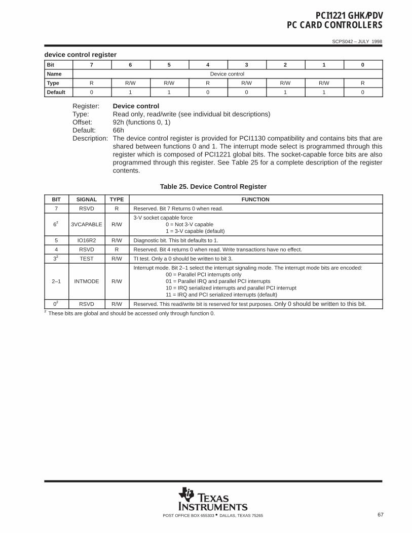
PCI1221 GHK/PDVPC CARD CONTROLLERS
SCPS042 – JULY 1998
67POST OFFICE BOX 655303 • DALLAS, TEXAS 75265
device control registerBit 7 6 5 4 3 2 1 0
Name Device control
Type R R/W R/W R R/W R/W R/W R
Default 0 1 1 0 0 1 1 0
Register: Device controlType: Read only, read/write (see individual bit descriptions)Offset: 92h (functions 0, 1)Default: 66hDescription: The device control register is provided for PCI1130 compatibility and contains bits that are
shared between functions 0 and 1. The interrupt mode select is programmed through thisregister which is composed of PCI1221 global bits. The socket-capable force bits are alsoprogrammed through this register. See Table 25 for a complete description of the registercontents.
Table 25. Device Control Register
BIT SIGNAL TYPE FUNCTION
7 RSVD R Reserved. Bit 7 Returns 0 when read.
6† 3VCAPABLE R/W3-V socket capable force
0 = Not 3-V capable1 = 3-V capable (default)
5 IO16R2 R/W Diagnostic bit. This bit defaults to 1.
4 RSVD R Reserved. Bit 4 returns 0 when read. Write transactions have no effect.
3† TEST R/W TI test. Only a 0 should be written to bit 3.
2–1 INTMODE R/W
Interrupt mode. Bit 2–1 select the interrupt signaling mode. The interrupt mode bits are encoded:00 = Parallel PCI interrupts only01 = Parallel IRQ and parallel PCI interrupts10 = IRQ serialized interrupts and parallel PCI interrupt11 = IRQ and PCI serialized interrupts (default)
0† RSVD R/W Reserved. This read/write bit is reserved for test purposes. Only 0 should be written to this bit.† These bits are global and should be accessed only through function 0.
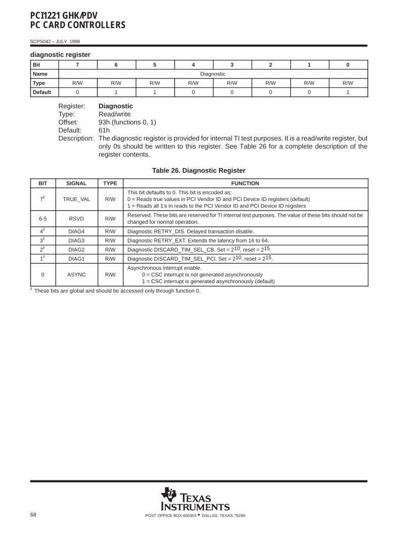
PCI1221 GHK/PDVPC CARD CONTROLLERS
SCPS042 – JULY 1998
68 POST OFFICE BOX 655303 • DALLAS, TEXAS 75265
diagnostic registerBit 7 6 5 4 3 2 1 0
Name Diagnostic
Type R/W R/W R/W R/W R/W R/W R/W R/W
Default 0 1 1 0 0 0 0 1
Register: DiagnosticType: Read/writeOffset: 93h (functions 0, 1)Default: 61hDescription: The diagnostic register is provided for internal TI test purposes. It is a read/write register, but
only 0s should be written to this register. See Table 26 for a complete description of theregister contents.
Table 26. Diagnostic Register
BIT SIGNAL TYPE FUNCTION
7† TRUE_VAL R/WThis bit defaults to 0. This bit is encoded as:0 = Reads true values in PCI Vendor ID and PCI Device ID registers (default)1 = Reads all 1’s in reads to the PCI Vendor ID and PCI Device ID registers
6-5 RSVD R/WReserved. These bits are reserved for TI internal test purposes. The value of these bits should not bechanged for normal operation.
4† DIAG4 R/W Diagnostic RETRY_DIS. Delayed transaction disable.
3† DIAG3 R/W Diagnostic RETRY_EXT. Extends the latency from 16 to 64.
2† DIAG2 R/W Diagnostic DISCARD_TIM_SEL_CB. Set = 210, reset = 215.
1† DIAG1 R/W Diagnostic DISCARD_TIM_SEL_PCI. Set = 210, reset = 215.
0 ASYNC R/WAsynchronous interrupt enable. 0 = CSC interrupt is not generated asynchronously 1 = CSC interrupt is generated asynchronously (default)
† These bits are global and should be accessed only through function 0.
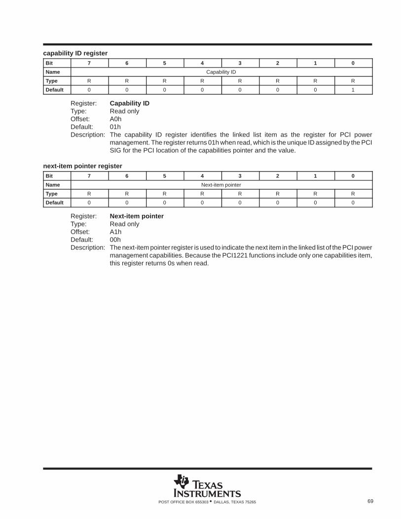
69POST OFFICE BOX 655303 • DALLAS, TEXAS 75265
capability ID registerBit 7 6 5 4 3 2 1 0
Name Capability ID
Type R R R R R R R R
Default 0 0 0 0 0 0 0 1
Register: Capability IDType: Read onlyOffset: A0hDefault: 01hDescription: The capability ID register identifies the linked list item as the register for PCI power
management. The register returns 01h when read, which is the unique ID assigned by the PCISIG for the PCI location of the capabilities pointer and the value.
next-item pointer registerBit 7 6 5 4 3 2 1 0
Name Next-item pointer
Type R R R R R R R R
Default 0 0 0 0 0 0 0 0
Register: Next-item pointerType: Read onlyOffset: A1hDefault: 00hDescription: The next-item pointer register is used to indicate the next item in the linked list of the PCI power
management capabilities. Because the PCI1221 functions include only one capabilities item,this register returns 0s when read.
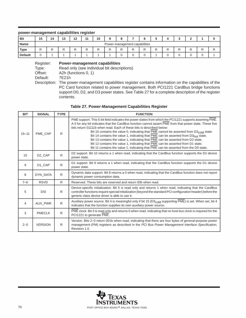
70 POST OFFICE BOX 655303 • DALLAS, TEXAS 75265
power-management capabilities registerBit 15 14 13 12 11 10 9 8 7 6 5 4 3 2 1 0
Name Power-management capabilities
Type R R R R R R R R R R R R R R R R
Default 0 1 1 1 1 1 1 0 0 0 1 0 0 0 0 1
Register: Power-management capabilitiesType: Read only (see individual bit descriptions)Offset: A2h (functions 0, 1)Default: 7E21hDescription: The power-management capabilities register contains information on the capabilities of the
PC Card function related to power management. Both PCI1221 CardBus bridge functionssupport D0, D2, and D3 power states. See Table 27 for a complete description of the registercontents.
Table 27. Power-Management Capabilities Register
BIT SIGNAL TYPE FUNCTION
15–11 PME_CAP R
PME support. This 5-bit field indicates the power states from which the PCI1221 supports asserting PME.A 0 for any bit indicates that the CardBus function cannot assert PME from that power state. These fivebits return 01111b when read. Each of these bits is described below:
Bit 15 contains the value 0, indicating that PME cannot be asserted from D3cold state.Bit 14 contains the value 1, indicating that PME can be asserted from D3hot state.Bit 13 contains the value 1, indicating that PME can be asserted from D2 state.Bit 12 contains the value 1, indicating that PME can be asserted from D1 state.Bit 11 contains the value 1, indicating that PME can be asserted from the D0 state.
10 D2_CAP RD2 support. Bit 10 returns a 1 when read, indicating that the CardBus function supports the D2 devicepower state.
9 D1_CAP RD1 support. Bit 9 returns a 1 when read, indicating that the CardBus function supports the D1 devicepower state.
8 DYN_DATA RDynamic data support. Bit 8 returns a 0 when read, indicating that the CardBus function does not reportdynamic power consumption data.
7–6 RSVD R Reserved. These bits are reserved and return 00b when read.
5 DSI RDevice-specific initialization. Bit 5 is read only and returns 1 when read, indicating that the CardBuscontroller functions require special initialization (beyond the standard PCI configuration header) before thegeneric class device driver is able to use it.
4 AUX_PWR RAuxiliary power source. Bit 4 is meaningful only if bit 15 (D3cold supporting PME) is set. When set, bit 4indicates that the function supplies its own auxiliary power source.
3 PMECLK RPME clock. Bit 3 is read only and returns 0 when read, indicating that no host bus clock is required for thePCI1221 to generate PME.
2–0 VERSION RVersion. Bits 2–0 return 001b when read, indicating that there are four bytes of general-purpose powermanagement (PM) registers as described in the PCI Bus Power Management Interface Specification,Revision 1.0.
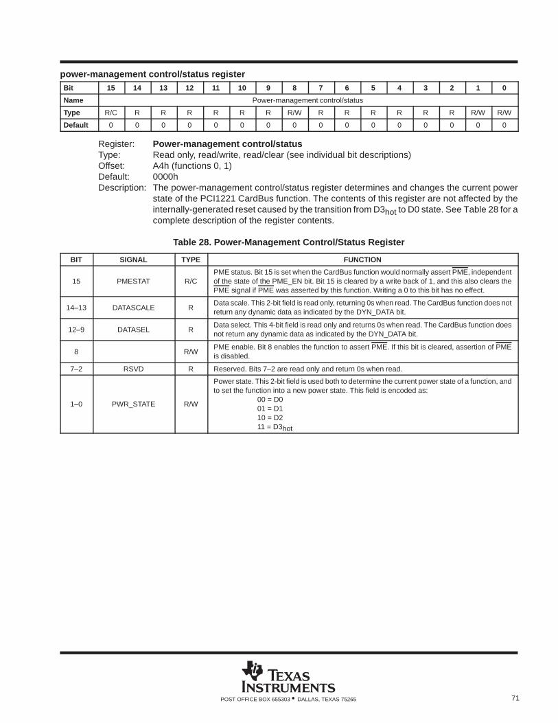
71POST OFFICE BOX 655303 • DALLAS, TEXAS 75265
power-management control/status registerBit 15 14 13 12 11 10 9 8 7 6 5 4 3 2 1 0
Name Power-management control/status
Type R/C R R R R R R R/W R R R R R R R/W R/W
Default 0 0 0 0 0 0 0 0 0 0 0 0 0 0 0 0
Register: Power-management control/statusType: Read only, read/write, read/clear (see individual bit descriptions)Offset: A4h (functions 0, 1)Default: 0000hDescription: The power-management control/status register determines and changes the current power
state of the PCI1221 CardBus function. The contents of this register are not affected by theinternally-generated reset caused by the transition from D3hot to D0 state. See Table 28 for acomplete description of the register contents.
Table 28. Power-Management Control/Status Register
BIT SIGNAL TYPE FUNCTION
15 PMESTAT R/CPME status. Bit 15 is set when the CardBus function would normally assert PME, independentof the state of the PME_EN bit. Bit 15 is cleared by a write back of 1, and this also clears thePME signal if PME was asserted by this function. Writing a 0 to this bit has no effect.
14–13 DATASCALE RData scale. This 2-bit field is read only, returning 0s when read. The CardBus function does notreturn any dynamic data as indicated by the DYN_DATA bit.
12–9 DATASEL RData select. This 4-bit field is read only and returns 0s when read. The CardBus function doesnot return any dynamic data as indicated by the DYN_DATA bit.
8 R/WPME enable. Bit 8 enables the function to assert PME. If this bit is cleared, assertion of PMEis disabled.
7–2 RSVD R Reserved. Bits 7–2 are read only and return 0s when read.
1–0 PWR_STATE R/W
Power state. This 2-bit field is used both to determine the current power state of a function, andto set the function into a new power state. This field is encoded as:
00 = D0 01 = D110 = D211 = D3hot
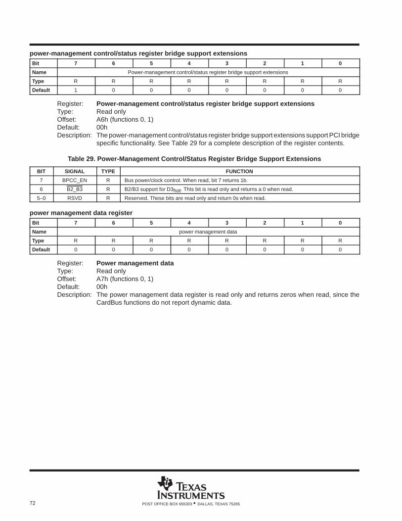
72 POST OFFICE BOX 655303 • DALLAS, TEXAS 75265
power-management control/status register bridge support extensionsBit 7 6 5 4 3 2 1 0
Name Power-management control/status register bridge support extensions
Type R R R R R R R R
Default 1 0 0 0 0 0 0 0
Register: Power-management control/status register bridge support extensionsType: Read onlyOffset: A6h (functions 0, 1)Default: 00hDescription: The power-management control/status register bridge support extensions support PCI bridge
specific functionality. See Table 29 for a complete description of the register contents.
Table 29. Power-Management Control/Status Register Bridge Support Extensions
BIT SIGNAL TYPE FUNCTION
7 BPCC_EN R Bus power/clock control. When read, bit 7 returns 1b.
6 B2_B3 R B2/B3 support for D3hot. ThIs bit is read only and returns a 0 when read.
5–0 RSVD R Reserved. These bits are read only and return 0s when read.
power management data registerBit 7 6 5 4 3 2 1 0
Name power management data
Type R R R R R R R R
Default 0 0 0 0 0 0 0 0
Register: Power management dataType: Read onlyOffset: A7h (functions 0, 1)Default: 00hDescription: The power management data register is read only and returns zeros when read, since the
CardBus functions do not report dynamic data.
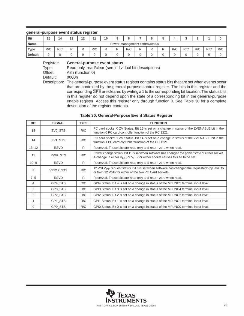
73POST OFFICE BOX 655303 • DALLAS, TEXAS 75265
general-purpose event status registerBit 15 14 13 12 11 10 9 8 7 6 5 4 3 2 1 0
Name Power-management control/status
Type R/C R/C R R R/C R R R/C R R R R/C R/C R/C R/C R/C
Default 0 0 0 0 0 0 0 0 0 0 0 0 0 0 0 0
Register: General-purpose event statusType: Read only, read/clear (see individual bit descriptions)Offset: A8h (function 0)Default: 0000hDescription: The general-purpose event status register contains status bits that are set when events occur
that are controlled by the general-purpose control register. The bits in this register and thecorresponding GPE are cleared by writing a 1 to the corresponding bit location. The status bitsin this register do not depend upon the state of a corresponding bit in the general-purposeenable register. Access this register only through function 0. See Table 30 for a completedescription of the register contents.
Table 30. General-Purpose Event Status Register
BIT SIGNAL TYPE FUNCTION
15 ZV0_STS R/CPC card socket 0 ZV Status. Bit 15 is set on a change in status of the ZVENABLE bit in thefunction 0 PC card controller function of the PCI1221.
14 ZV1_STS R/CPC card socket 1 ZV Status. Bit 14 is set on a change in status of the ZVENABLE bit in thefunction 1 PC card controller function of the PCI1221.
13–12 RSVD R Reserved. These bits are read only and return zero when read.
11 PWR_STS R/CPower change status. Bit 11 is set when software has changed the power state of either socket.A change in either VCC or VPP for either socket causes this bit to be set.
10–9 RSVD R Reserved. These bits are read only and return zero when read.
8 VPP12_STS R/C12 Volt VPP request status. Bit 8 is set when software has changed the requested Vpp level toor from 12 Volts for either of the two PC Card sockets.
7–5 RSVD R Reserved. These bits are read only and return zero when read.
4 GP4_STS R/C GPI4 Status. Bit 4 is set on a change in status of the MFUNC5 terminal input level.
3 GP3_STS R/C GPI3 Status. Bit 3 is set on a change in status of the MFUNC4 terminal input level .
2 GP2_STS R/C GPI2 Status. Bit 2 is set on a change in status of the MFUNC2 terminal input level.
1 GP1_STS R/C GPI1 Status. Bit 1 is set on a change in status of the MFUNC1 terminal input level.
0 GP0_STS R/C GPI0 Status. Bit 0 is set on a change in status of the MFUNC0 terminal input level.
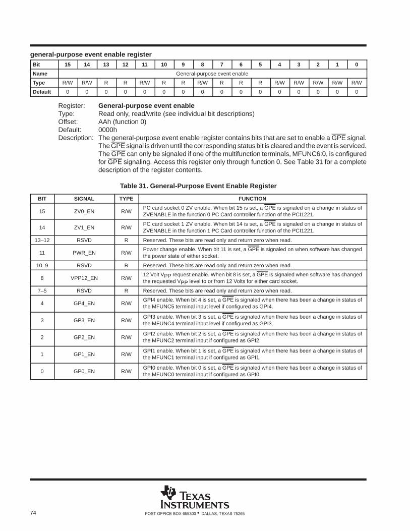
74 POST OFFICE BOX 655303 • DALLAS, TEXAS 75265
general-purpose event enable registerBit 15 14 13 12 11 10 9 8 7 6 5 4 3 2 1 0
Name General-purpose event enable
Type R/W R/W R R R/W R R R/W R R R R/W R/W R/W R/W R/W
Default 0 0 0 0 0 0 0 0 0 0 0 0 0 0 0 0
Register: General-purpose event enableType: Read only, read/write (see individual bit descriptions)Offset: AAh (function 0)Default: 0000hDescription: The general-purpose event enable register contains bits that are set to enable a GPE signal.
The GPE signal is driven until the corresponding status bit is cleared and the event is serviced.The GPE can only be signaled if one of the multifunction terminals, MFUNC6:0, is configuredfor GPE signaling. Access this register only through function 0. See Table 31 for a completedescription of the register contents.
Table 31. General-Purpose Event Enable Register
BIT SIGNAL TYPE FUNCTION
15 ZV0_EN R/WPC card socket 0 ZV enable. When bit 15 is set, a GPE is signaled on a change in status ofZVENABLE in the function 0 PC Card controller function of the PCI1221.
14 ZV1_EN R/WPC card socket 1 ZV enable. When bit 14 is set, a GPE is signaled on a change in status ofZVENABLE in the function 1 PC Card controller function of the PCI1221.
13–12 RSVD R Reserved. These bits are read only and return zero when read.
11 PWR_EN R/WPower change enable. When bit 11 is set, a GPE is signaled on when software has changedthe power state of either socket.
10–9 RSVD R Reserved. These bits are read only and return zero when read.
8 VPP12_EN R/W12 Volt VPP request enable. When bit 8 is set, a GPE is signaled when software has changedthe requested VPP level to or from 12 Volts for either card socket.
7–5 RSVD R Reserved. These bits are read only and return zero when read.
4 GP4_EN R/WGPI4 enable. When bit 4 is set, a GPE is signaled when there has been a change in status ofthe MFUNC5 terminal input level if configured as GPI4.
3 GP3_EN R/WGPI3 enable. When bit 3 is set, a GPE is signaled when there has been a change in status ofthe MFUNC4 terminal input level if configured as GPI3.
2 GP2_EN R/WGPI2 enable. When bit 2 is set, a GPE is signaled when there has been a change in status ofthe MFUNC2 terminal input if configured as GPI2.
1 GP1_EN R/WGPI1 enable. When bit 1 is set, a GPE is signaled when there has been a change in status ofthe MFUNC1 terminal input if configured as GPI1.
0 GP0_EN R/WGPI0 enable. When bit 0 is set, a GPE is signaled when there has been a change in status ofthe MFUNC0 terminal input if configured as GPI0.
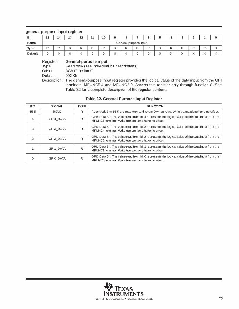
75POST OFFICE BOX 655303 • DALLAS, TEXAS 75265
general-purpose input registerBit 15 14 13 12 11 10 9 8 7 6 5 4 3 2 1 0
Name General-purpose input
Type R R R R R R R R R R R R R R R R
Default 0 0 0 0 0 0 0 0 0 0 0 X X X X X
Register: General-purpose inputType: Read only (see individual bit descriptions)Offset: ACh (function 0)Default: 00XXhDescription: The general-purpose input register provides the logical value of the data input from the GPI
terminals, MFUNC5:4 and MFUNC2:0. Access this register only through function 0. SeeTable 32 for a complete description of the register contents.
Table 32. General-Purpose Input Register
BIT SIGNAL TYPE FUNCTION
15-5 RSVD R Reserved. Bits 15-5 are read only and return 0 when read. Write transactions have no effect.
4 GPI4_DATA RGPI4 Data Bit. The value read from bit 4 represents the logical value of the data input from theMFUNC5 terminal. Write transactions have no effect.
3 GPI3_DATA RGPI3 Data Bit. The value read from bit 3 represents the logical value of the data input from theMFUNC4 terminal. Write transactions have no effect.
2 GPI2_DATA RGPI2 Data Bit. The value read from bit 2 represents the logical value of the data input from theMFUNC2 terminal. Write transactions have no effect.
1 GPI1_DATA RGPI1 Data Bit. The value read from bit 1 represents the logical value of the data input from theMFUNC1 terminal. Write transactions have no effect.
0 GPI0_DATA RGPI0 Data Bit. The value read from bit 0 represents the logical value of the data input from theMFUNC0 terminal. Write transactions have no effect.
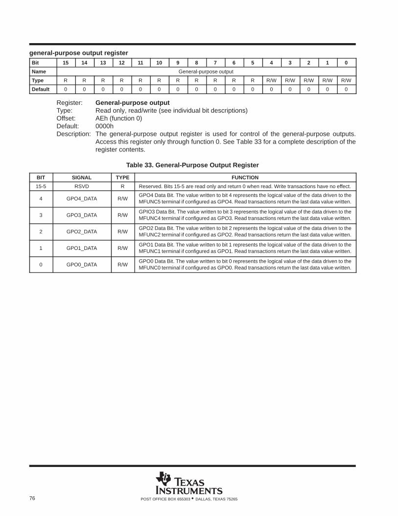
76 POST OFFICE BOX 655303 • DALLAS, TEXAS 75265
general-purpose output registerBit 15 14 13 12 11 10 9 8 7 6 5 4 3 2 1 0
Name General-purpose output
Type R R R R R R R R R R R R/W R/W R/W R/W R/W
Default 0 0 0 0 0 0 0 0 0 0 0 0 0 0 0 0
Register: General-purpose outputType: Read only, read/write (see individual bit descriptions)Offset: AEh (function 0)Default: 0000hDescription: The general-purpose output register is used for control of the general-purpose outputs.
Access this register only through function 0. See Table 33 for a complete description of theregister contents.
Table 33. General-Purpose Output Register
BIT SIGNAL TYPE FUNCTION
15-5 RSVD R Reserved. Bits 15-5 are read only and return 0 when read. Write transactions have no effect.
4 GPO4_DATA R/WGPO4 Data Bit. The value written to bit 4 represents the logical value of the data driven to theMFUNC5 terminal if configured as GPO4. Read transactions return the last data value written.
3 GPO3_DATA R/WGPIO3 Data Bit. The value written to bit 3 represents the logical value of the data driven to theMFUNC4 terminal if configured as GPO3. Read transactions return the last data value written.
2 GPO2_DATA R/WGPO2 Data Bit. The value written to bit 2 represents the logical value of the data driven to theMFUNC2 terminal if configured as GPO2. Read transactions return the last data value written.
1 GPO1_DATA R/WGPO1 Data Bit. The value written to bit 1 represents the logical value of the data driven to theMFUNC1 terminal if configured as GPO1. Read transactions return the last data value written.
0 GPO0_DATA R/WGPO0 Data Bit. The value written to bit 0 represents the logical value of the data driven to theMFUNC0 terminal if configured as GPO0. Read transactions return the last data value written.
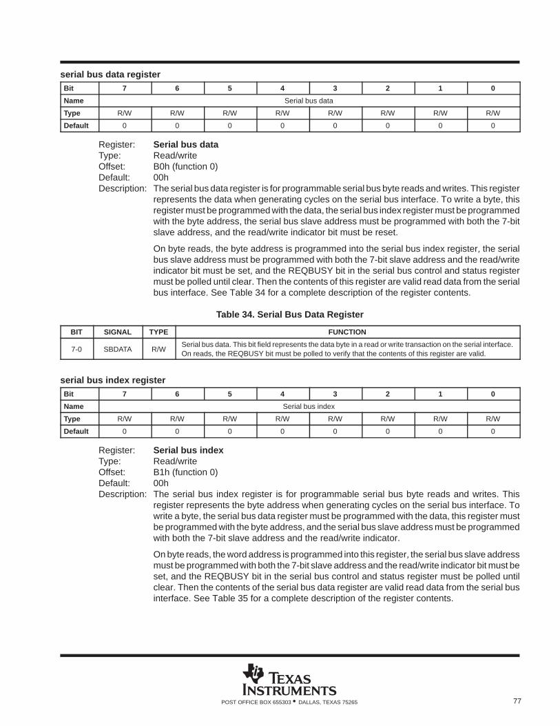
77POST OFFICE BOX 655303 • DALLAS, TEXAS 75265
serial bus data registerBit 7 6 5 4 3 2 1 0
Name Serial bus data
Type R/W R/W R/W R/W R/W R/W R/W R/W
Default 0 0 0 0 0 0 0 0
Register: Serial bus dataType: Read/writeOffset: B0h (function 0)Default: 00hDescription: The serial bus data register is for programmable serial bus byte reads and writes. This register
represents the data when generating cycles on the serial bus interface. To write a byte, thisregister must be programmed with the data, the serial bus index register must be programmedwith the byte address, the serial bus slave address must be programmed with both the 7-bitslave address, and the read/write indicator bit must be reset.
On byte reads, the byte address is programmed into the serial bus index register, the serialbus slave address must be programmed with both the 7-bit slave address and the read/writeindicator bit must be set, and the REQBUSY bit in the serial bus control and status registermust be polled until clear. Then the contents of this register are valid read data from the serialbus interface. See Table 34 for a complete description of the register contents.
Table 34. Serial Bus Data Register
BIT SIGNAL TYPE FUNCTION
7-0 SBDATA R/WSerial bus data. This bit field represents the data byte in a read or write transaction on the serial interface.On reads, the REQBUSY bit must be polled to verify that the contents of this register are valid.
serial bus index registerBit 7 6 5 4 3 2 1 0
Name Serial bus index
Type R/W R/W R/W R/W R/W R/W R/W R/W
Default 0 0 0 0 0 0 0 0
Register: Serial bus indexType: Read/writeOffset: B1h (function 0)Default: 00hDescription: The serial bus index register is for programmable serial bus byte reads and writes. This
register represents the byte address when generating cycles on the serial bus interface. Towrite a byte, the serial bus data register must be programmed with the data, this register mustbe programmed with the byte address, and the serial bus slave address must be programmedwith both the 7-bit slave address and the read/write indicator.
On byte reads, the word address is programmed into this register, the serial bus slave addressmust be programmed with both the 7-bit slave address and the read/write indicator bit must beset, and the REQBUSY bit in the serial bus control and status register must be polled untilclear. Then the contents of the serial bus data register are valid read data from the serial businterface. See Table 35 for a complete description of the register contents.
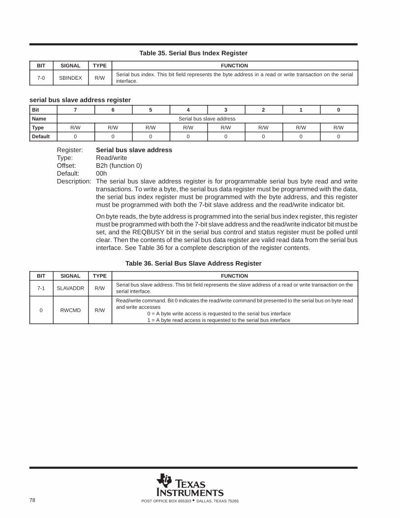
78 POST OFFICE BOX 655303 • DALLAS, TEXAS 75265
Table 35. Serial Bus Index Register
BIT SIGNAL TYPE FUNCTION
7-0 SBINDEX R/WSerial bus index. This bit field represents the byte address in a read or write transaction on the serialinterface.
serial bus slave address registerBit 7 6 5 4 3 2 1 0
Name Serial bus slave address
Type R/W R/W R/W R/W R/W R/W R/W R/W
Default 0 0 0 0 0 0 0 0
Register: Serial bus slave addressType: Read/writeOffset: B2h (function 0)Default: 00hDescription: The serial bus slave address register is for programmable serial bus byte read and write
transactions. To write a byte, the serial bus data register must be programmed with the data,the serial bus index register must be programmed with the byte address, and this registermust be programmed with both the 7-bit slave address and the read/write indicator bit.
On byte reads, the byte address is programmed into the serial bus index register, this registermust be programmed with both the 7-bit slave address and the read/write indicator bit must beset, and the REQBUSY bit in the serial bus control and status register must be polled untilclear. Then the contents of the serial bus data register are valid read data from the serial businterface. See Table 36 for a complete description of the register contents.
Table 36. Serial Bus Slave Address Register
BIT SIGNAL TYPE FUNCTION
7-1 SLAVADDR R/WSerial bus slave address. This bit field represents the slave address of a read or write transaction on theserial interface.
0 RWCMD R/W
Read/write command. Bit 0 indicates the read/write command bit presented to the serial bus on byte readand write accesses
0 = A byte write access is requested to the serial bus interface1 = A byte read access is requested to the serial bus interface
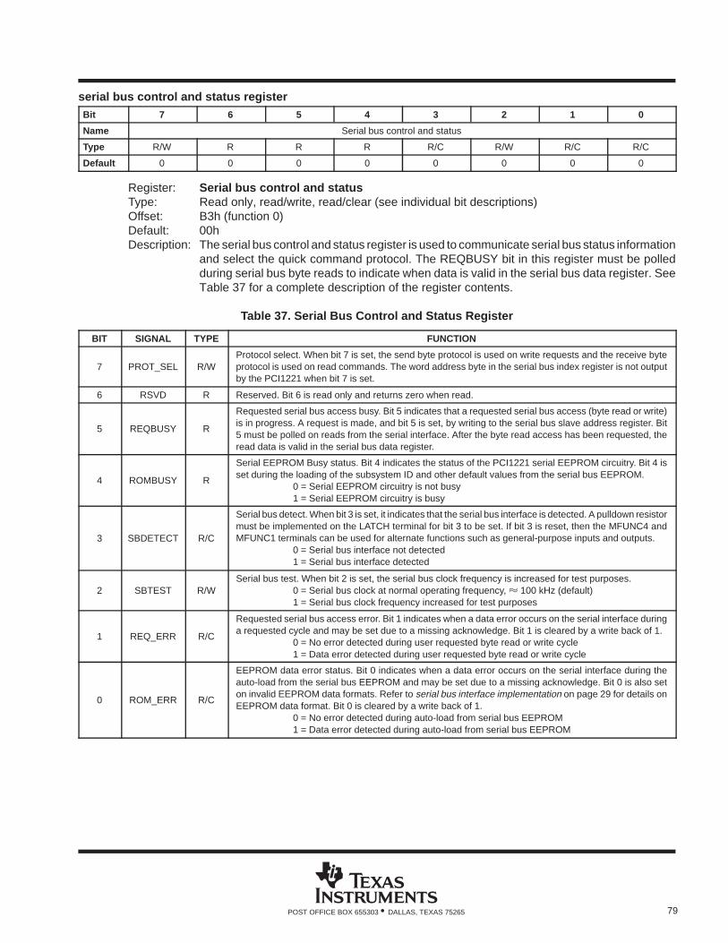
79POST OFFICE BOX 655303 • DALLAS, TEXAS 75265
serial bus control and status registerBit 7 6 5 4 3 2 1 0
Name Serial bus control and status
Type R/W R R R R/C R/W R/C R/C
Default 0 0 0 0 0 0 0 0
Register: Serial bus control and statusType: Read only, read/write, read/clear (see individual bit descriptions)Offset: B3h (function 0)Default: 00hDescription: The serial bus control and status register is used to communicate serial bus status information
and select the quick command protocol. The REQBUSY bit in this register must be polledduring serial bus byte reads to indicate when data is valid in the serial bus data register. SeeTable 37 for a complete description of the register contents.
Table 37. Serial Bus Control and Status Register
BIT SIGNAL TYPE FUNCTION
7 PROT_SEL R/WProtocol select. When bit 7 is set, the send byte protocol is used on write requests and the receive byteprotocol is used on read commands. The word address byte in the serial bus index register is not outputby the PCI1221 when bit 7 is set.
6 RSVD R Reserved. Bit 6 is read only and returns zero when read.
5 REQBUSY R
Requested serial bus access busy. Bit 5 indicates that a requested serial bus access (byte read or write)is in progress. A request is made, and bit 5 is set, by writing to the serial bus slave address register. Bit5 must be polled on reads from the serial interface. After the byte read access has been requested, theread data is valid in the serial bus data register.
4 ROMBUSY R
Serial EEPROM Busy status. Bit 4 indicates the status of the PCI1221 serial EEPROM circuitry. Bit 4 isset during the loading of the subsystem ID and other default values from the serial bus EEPROM.
0 = Serial EEPROM circuitry is not busy1 = Serial EEPROM circuitry is busy
3 SBDETECT R/C
Serial bus detect. When bit 3 is set, it indicates that the serial bus interface is detected. A pulldown resistormust be implemented on the LATCH terminal for bit 3 to be set. If bit 3 is reset, then the MFUNC4 andMFUNC1 terminals can be used for alternate functions such as general-purpose inputs and outputs.
0 = Serial bus interface not detected1 = Serial bus interface detected
2 SBTEST R/WSerial bus test. When bit 2 is set, the serial bus clock frequency is increased for test purposes.
0 = Serial bus clock at normal operating frequency, 100 kHz (default)1 = Serial bus clock frequency increased for test purposes
1 REQ_ERR R/C
Requested serial bus access error. Bit 1 indicates when a data error occurs on the serial interface duringa requested cycle and may be set due to a missing acknowledge. Bit 1 is cleared by a write back of 1.
0 = No error detected during user requested byte read or write cycle1 = Data error detected during user requested byte read or write cycle
0 ROM_ERR R/C
EEPROM data error status. Bit 0 indicates when a data error occurs on the serial interface during theauto-load from the serial bus EEPROM and may be set due to a missing acknowledge. Bit 0 is also seton invalid EEPROM data formats. Refer to serial bus interface implementation on page 29 for details onEEPROM data format. Bit 0 is cleared by a write back of 1.
0 = No error detected during auto-load from serial bus EEPROM1 = Data error detected during auto-load from serial bus EEPROM
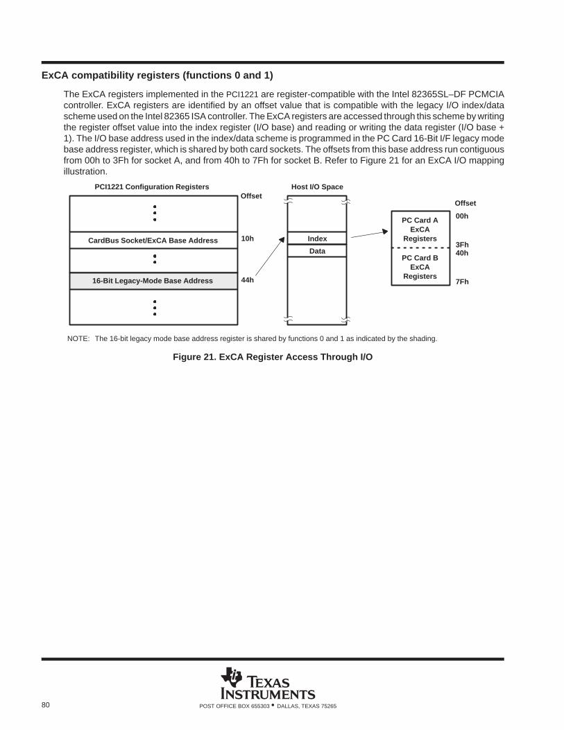
80 POST OFFICE BOX 655303 • DALLAS, TEXAS 75265
ExCA compatibility registers (functions 0 and 1)
The ExCA registers implemented in the PCI1221 are register-compatible with the Intel 82365SL–DF PCMCIAcontroller. ExCA registers are identified by an offset value that is compatible with the legacy I/O index/datascheme used on the Intel 82365 ISA controller. The ExCA registers are accessed through this scheme by writingthe register offset value into the index register (I/O base) and reading or writing the data register (I/O base +1). The I/O base address used in the index/data scheme is programmed in the PC Card 16-Bit I/F legacy modebase address register, which is shared by both card sockets. The offsets from this base address run contiguousfrom 00h to 3Fh for socket A, and from 40h to 7Fh for socket B. Refer to Figure 21 for an ExCA I/O mappingillustration.
CardBus Socket/ExCA Base Address
16-Bit Legacy-Mode Base Address
10h
44h
00h
3Fh
Offset
Index
Host I/O Space
Data
PC Card AExCA
Registers
PC Card BExCA
Registers
40h
7Fh
NOTE: The 16-bit legacy mode base address register is shared by functions 0 and 1 as indicated by the shading.
PCI1221 Configuration RegistersOffset
Figure 21. ExCA Register Access Through I/O
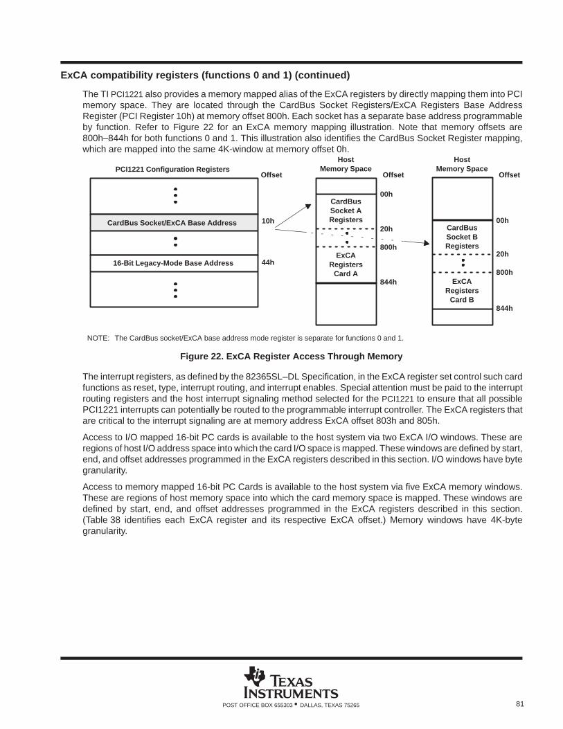
81POST OFFICE BOX 655303 • DALLAS, TEXAS 75265
ExCA compatibility registers (functions 0 and 1) (continued)
The TI PCI1221 also provides a memory mapped alias of the ExCA registers by directly mapping them into PCImemory space. They are located through the CardBus Socket Registers/ExCA Registers Base AddressRegister (PCI Register 10h) at memory offset 800h. Each socket has a separate base address programmableby function. Refer to Figure 22 for an ExCA memory mapping illustration. Note that memory offsets are800h–844h for both functions 0 and 1. This illustration also identifies the CardBus Socket Register mapping,which are mapped into the same 4K-window at memory offset 0h.
CardBus Socket/ExCA Base Address
16-Bit Legacy-Mode Base Address
10h
44h
NOTE: The CardBus socket/ExCA base address mode register is separate for functions 0 and 1.
PCI1221 Configuration Registers
CardBusSocket ARegisters
HostMemory Space
00h
ExCARegisters
Card A
20h
800h
844h
Offset
CardBusSocket BRegisters
HostMemory Space
00h
ExCARegisters
Card B
20h
800h
844h
OffsetOffset
Figure 22. ExCA Register Access Through Memory
The interrupt registers, as defined by the 82365SL–DL Specification, in the ExCA register set control such cardfunctions as reset, type, interrupt routing, and interrupt enables. Special attention must be paid to the interruptrouting registers and the host interrupt signaling method selected for the PCI1221 to ensure that all possiblePCI1221 interrupts can potentially be routed to the programmable interrupt controller. The ExCA registers thatare critical to the interrupt signaling are at memory address ExCA offset 803h and 805h.
Access to I/O mapped 16-bit PC cards is available to the host system via two ExCA I/O windows. These areregions of host I/O address space into which the card I/O space is mapped. These windows are defined by start,end, and offset addresses programmed in the ExCA registers described in this section. I/O windows have bytegranularity.
Access to memory mapped 16-bit PC Cards is available to the host system via five ExCA memory windows.These are regions of host memory space into which the card memory space is mapped. These windows aredefined by start, end, and offset addresses programmed in the ExCA registers described in this section.(Table 38 identifies each ExCA register and its respective ExCA offset.) Memory windows have 4K-bytegranularity.
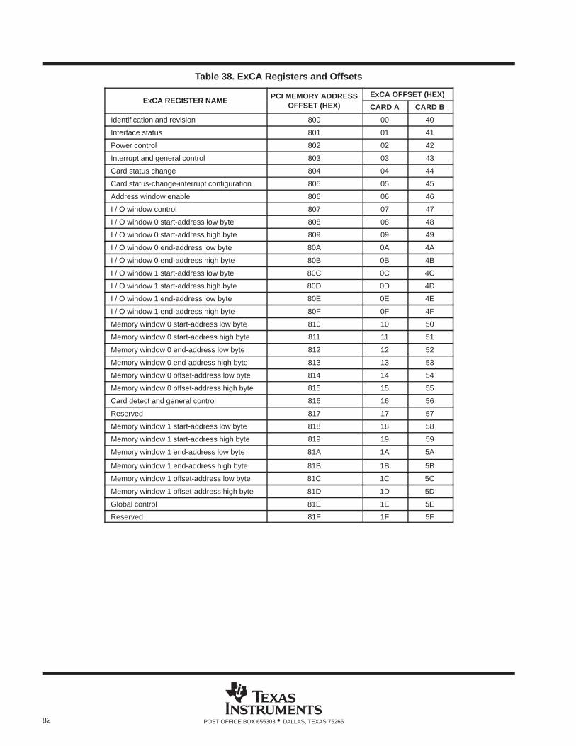
82 POST OFFICE BOX 655303 • DALLAS, TEXAS 75265
Table 38. ExCA Registers and Offsets
EXCA REGISTER NAMEPCI MEMORY ADDRESS ExCA OFFSET (HEX)
EXCA REGISTER NAMEOFFSET (HEX) CARD A CARD B
Identification and revision 800 00 40
Interface status 801 01 41
Power control 802 02 42
Interrupt and general control 803 03 43
Card status change 804 04 44
Card status-change-interrupt configuration 805 05 45
Address window enable 806 06 46
I / O window control 807 07 47
I / O window 0 start-address low byte 808 08 48
I / O window 0 start-address high byte 809 09 49
I / O window 0 end-address low byte 80A 0A 4A
I / O window 0 end-address high byte 80B 0B 4B
I / O window 1 start-address low byte 80C 0C 4C
I / O window 1 start-address high byte 80D 0D 4D
I / O window 1 end-address low byte 80E 0E 4E
I / O window 1 end-address high byte 80F 0F 4F
Memory window 0 start-address low byte 810 10 50
Memory window 0 start-address high byte 811 11 51
Memory window 0 end-address low byte 812 12 52
Memory window 0 end-address high byte 813 13 53
Memory window 0 offset-address low byte 814 14 54
Memory window 0 offset-address high byte 815 15 55
Card detect and general control 816 16 56
Reserved 817 17 57
Memory window 1 start-address low byte 818 18 58
Memory window 1 start-address high byte 819 19 59
Memory window 1 end-address low byte 81A 1A 5A
Memory window 1 end-address high byte 81B 1B 5B
Memory window 1 offset-address low byte 81C 1C 5C
Memory window 1 offset-address high byte 81D 1D 5D
Global control 81E 1E 5E
Reserved 81F 1F 5F
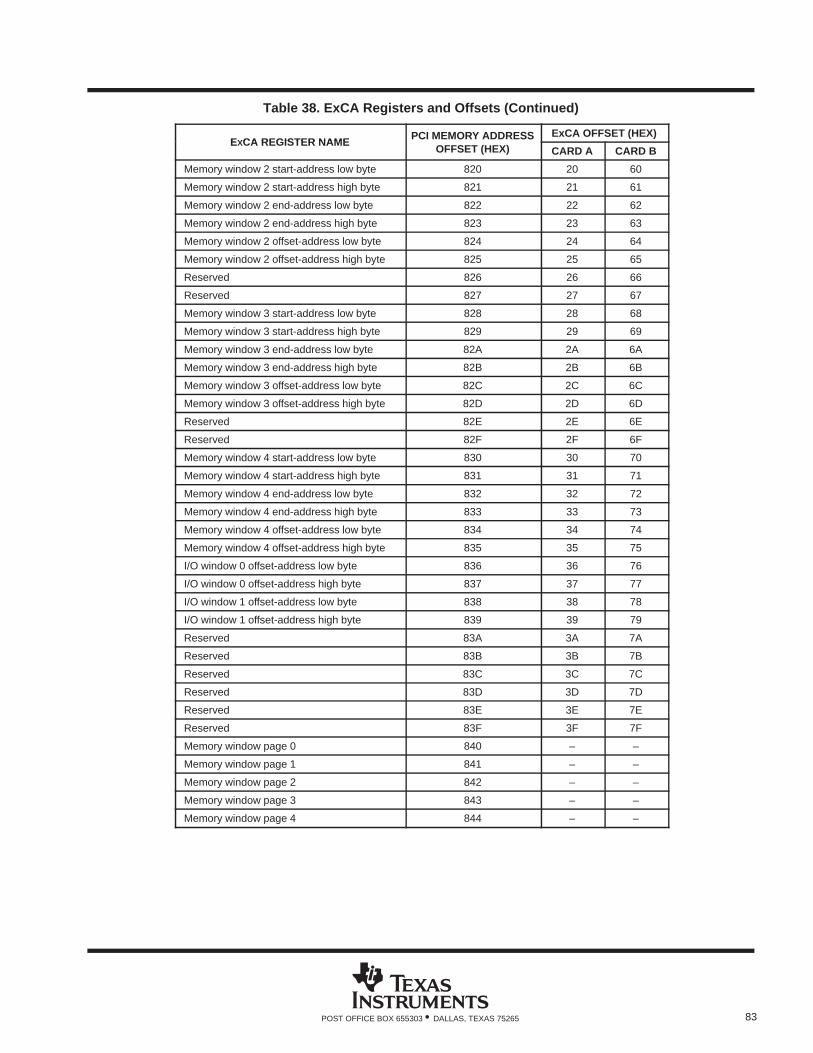
83POST OFFICE BOX 655303 • DALLAS, TEXAS 75265
Table 38. ExCA Registers and Offsets (Continued)
EXCA REGISTER NAMEPCI MEMORY ADDRESS ExCA OFFSET (HEX)
EXCA REGISTER NAMEOFFSET (HEX) CARD A CARD B
Memory window 2 start-address low byte 820 20 60
Memory window 2 start-address high byte 821 21 61
Memory window 2 end-address low byte 822 22 62
Memory window 2 end-address high byte 823 23 63
Memory window 2 offset-address low byte 824 24 64
Memory window 2 offset-address high byte 825 25 65
Reserved 826 26 66
Reserved 827 27 67
Memory window 3 start-address low byte 828 28 68
Memory window 3 start-address high byte 829 29 69
Memory window 3 end-address low byte 82A 2A 6A
Memory window 3 end-address high byte 82B 2B 6B
Memory window 3 offset-address low byte 82C 2C 6C
Memory window 3 offset-address high byte 82D 2D 6D
Reserved 82E 2E 6E
Reserved 82F 2F 6F
Memory window 4 start-address low byte 830 30 70
Memory window 4 start-address high byte 831 31 71
Memory window 4 end-address low byte 832 32 72
Memory window 4 end-address high byte 833 33 73
Memory window 4 offset-address low byte 834 34 74
Memory window 4 offset-address high byte 835 35 75
I/O window 0 offset-address low byte 836 36 76
I/O window 0 offset-address high byte 837 37 77
I/O window 1 offset-address low byte 838 38 78
I/O window 1 offset-address high byte 839 39 79
Reserved 83A 3A 7A
Reserved 83B 3B 7B
Reserved 83C 3C 7C
Reserved 83D 3D 7D
Reserved 83E 3E 7E
Reserved 83F 3F 7F
Memory window page 0 840 – –
Memory window page 1 841 – –
Memory window page 2 842 – –
Memory window page 3 843 – –
Memory window page 4 844 – –
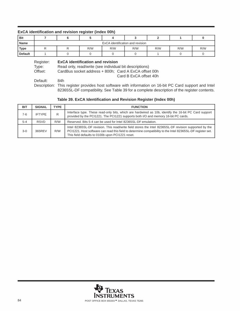
84 POST OFFICE BOX 655303 • DALLAS, TEXAS 75265
ExCA identification and revision register (index 00h)Bit 7 6 5 4 3 2 1 0
Name ExCA identification and revision
Type R R R/W R/W R/W R/W R/W R/W
Default 1 0 0 0 0 1 0 0
Register: ExCA identification and revisionType: Read only, read/write (see individual bit descriptions)Offset: CardBus socket address + 800h; Card A ExCA offset 00h
Card B ExCA offset 40hDefault: 84hDescription: This register provides host software with information on 16-bit PC Card support and Intel
82365SL-DF compatibility. See Table 39 for a complete description of the register contents.
Table 39. ExCA Identification and Revision Register (Index 00h)
BIT SIGNAL TYPE FUNCTION
7-6 IFTYPE RInterface type. These read-only bits, which are hardwired as 10b, identify the 16-bit PC Card supportprovided by the PCI1221. The PCI1221 supports both I/O and memory 16-bit PC cards.
5-4 RSVD R/W Reserved. Bits 5-4 can be used for Intel 82365SL-DF emulation.
3-0 365REV R/WIntel 82365SL-DF revision. This read/write field stores the Intel 82365SL-DF revision supported by thePCI1221. Host software can read this field to determine compatibility to the Intel 82365SL-DF register set.This field defaults to 0100b upon PCI1221 reset.
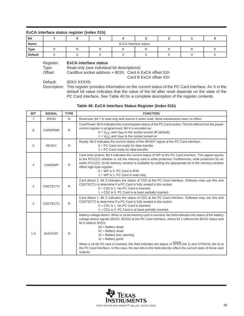
85POST OFFICE BOX 655303 • DALLAS, TEXAS 75265
ExCA interface status register (index 01h)Bit 7 6 5 4 3 2 1 0
Name ExCA interface status
Type R R R R R R R R
Default 0 0 X X X X X X
Register: ExCA interface statusType: Read only (see individual bit descriptions)Offset: CardBus socket address + 801h; Card A ExCA offset 01h
Card B ExCA offset 41hDefault: 00XX XXXXbDescription: This register provides information on the current status of the PC Card interface. An X in the
default bit value indicates that the value of the bit after reset depends on the state of thePC Card interface. See Table 40 for a complete description of the register contents.
Table 40. ExCA Interface Status Register (Index 01h)
BIT SIGNAL TYPE FUNCTION
7 RSVD R Reserved. Bit 7 is read only and returns 0 when read. Write transactions have no effect.
6 CARDPWR R
Card Power. Bit 6 indicates the current power status of the PC Card socket. This bit reflects how the powercontrol register is programmed. Bit 6 is encoded as:
0 = VCC and VPP to the socket turned off (default)1 = VCC and VPP to the socket turned on
5 READY RReady. Bit 5 indicates the current status of the READY signal at the PC Card interface.
0 = PC Card not ready for data transfer1 = PC Card ready for data transfer
4 CARDWP R
Card write protect. Bit 4 indicates the current status of WP at the PC Card interface. This signal reportsto the PCI1221 whether or not the memory card is write protected. Furthermore, write protection for anentire PCI1221 16-bit memory window is available by setting the appropriate bit in the memory windowoffset high-byte register.
0 = WP is 0. PC Card is R/W.1 = WP is 1. PC Card is read only.
3 CDETECT2 R
Card detect 2. Bit 3 indicates the status of CD2 at the PC Card interface. Software may use this andCDETECT1 to determine if a PC Card is fully seated in the socket.
0 = CD2 is 1. No PC Card is inserted.1 = CD2 is 0. PC Card is at least partially inserted.
2 CDETECT1 R
Card detect 1. Bit 2 indicates the status of CD1 at the PC Card interface. Software may use this andCDETECT2 to determine if a PC Card is fully seated in the socket.
0 = CD1 is 1. No PC Card is inserted.1 = CD1 is 0. PC Card is at least partially inserted.
1-0 BVDSTAT R
Battery voltage detect. When a 16-bit memory card is inserted, the field indicates the status of the batteryvoltage detect signals (BVD1, BVD2) at the PC Card interface, where bit 1 reflects the BVD2 status andbit 0 reflects BVD1.
00 = Battery dead01 = Battery dead10 = Battery low; warning11 = Battery good
When a 16-bit I/O card is inserted, this field indicates the status of SPKR (bit 1) and STSCHG (bit 0) atthe PC Card interface. In this case, the two bits in this field directly reflect the current state of these cardoutputs.
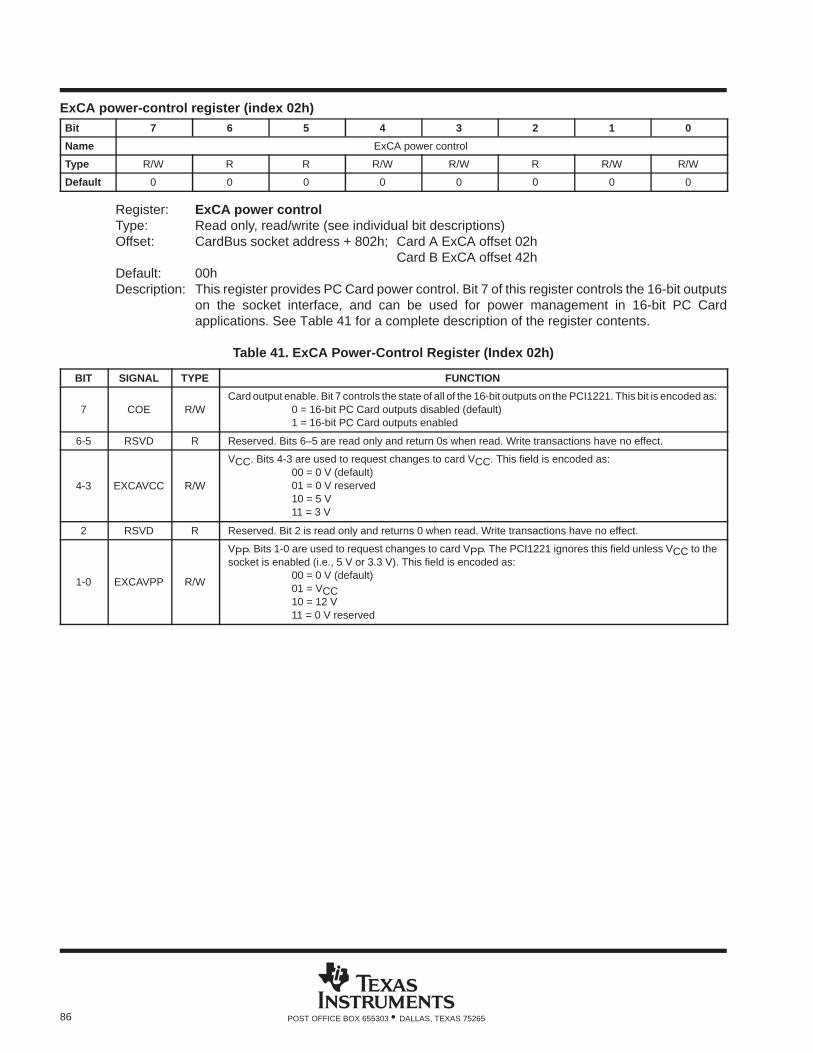
86 POST OFFICE BOX 655303 • DALLAS, TEXAS 75265
ExCA power-control register (index 02h)Bit 7 6 5 4 3 2 1 0
Name ExCA power control
Type R/W R R R/W R/W R R/W R/W
Default 0 0 0 0 0 0 0 0
Register: ExCA power controlType: Read only, read/write (see individual bit descriptions)Offset: CardBus socket address + 802h; Card A ExCA offset 02h
Card B ExCA offset 42hDefault: 00hDescription: This register provides PC Card power control. Bit 7 of this register controls the 16-bit outputs
on the socket interface, and can be used for power management in 16-bit PC Cardapplications. See Table 41 for a complete description of the register contents.
Table 41. ExCA Power-Control Register (Index 02h)
BIT SIGNAL TYPE FUNCTION
7 COE R/WCard output enable. Bit 7 controls the state of all of the 16-bit outputs on the PCI1221. This bit is encoded as:
0 = 16-bit PC Card outputs disabled (default)1 = 16-bit PC Card outputs enabled
6-5 RSVD R Reserved. Bits 6–5 are read only and return 0s when read. Write transactions have no effect.
4-3 EXCAVCC R/W
VCC. Bits 4-3 are used to request changes to card VCC. This field is encoded as:00 = 0 V (default)01 = 0 V reserved10 = 5 V11 = 3 V
2 RSVD R Reserved. Bit 2 is read only and returns 0 when read. Write transactions have no effect.
1-0 EXCAVPP R/W
VPP. Bits 1-0 are used to request changes to card VPP. The PCI1221 ignores this field unless VCC to thesocket is enabled (i.e., 5 V or 3.3 V). This field is encoded as:
00 = 0 V (default)01 = VCC10 = 12 V11 = 0 V reserved
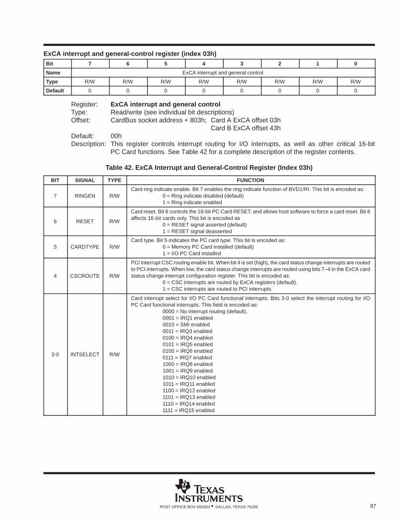
87POST OFFICE BOX 655303 • DALLAS, TEXAS 75265
ExCA interrupt and general-control register (index 03h)Bit 7 6 5 4 3 2 1 0
Name ExCA interrupt and general control
Type R/W R/W R/W R/W R/W R/W R/W R/W
Default 0 0 0 0 0 0 0 0
Register: ExCA interrupt and general controlType: Read/write (see individual bit descriptions)Offset: CardBus socket address + 803h; Card A ExCA offset 03h
Card B ExCA offset 43hDefault: 00hDescription: This register controls interrupt routing for I/O interrupts, as well as other critical 16-bit
PC Card functions. See Table 42 for a complete description of the register contents.
Table 42. ExCA Interrupt and General-Control Register (Index 03h)
BIT SIGNAL TYPE FUNCTION
7 RINGEN R/WCard ring indicate enable. Bit 7 enables the ring indicate function of BVD1/RI. This bit is encoded as:
0 = Ring indicate disabled (default)1 = Ring indicate enabled
6 RESET R/W
Card reset. Bit 6 controls the 16-bit PC Card RESET, and allows host software to force a card reset. Bit 6affects 16-bit cards only. This bit is encoded as
0 = RESET signal asserted (default)1 = RESET signal deasserted
5 CARDTYPE R/WCard type. Bit 5 indicates the PC card type. This bit is encoded as:
0 = Memory PC Card installed (default)1 = I/O PC Card installed
4 CSCROUTE R/W
PCI Interrupt CSC routing enable bit. When bit 4 is set (high), the card status change interrupts are routedto PCI interrupts. When low, the card status change interrupts are routed using bits 7–4 in the ExCA cardstatus change interrupt configuration register. This bit is encoded as:
0 = CSC interrupts are routed by ExCA registers (default).1 = CSC interrupts are routed to PCI interrupts.
3-0 INTSELECT R/W
Card interrupt select for I/O PC Card functional interrupts. Bits 3-0 select the interrupt routing for I/OPC Card functional interrupts. This field is encoded as:
0000 = No interrupt routing (default).0001 = IRQ1 enabled0010 = SMI enabled0011 = IRQ3 enabled0100 = IRQ4 enabled0101 = IRQ5 enabled0100 = IRQ6 enabled0111 = IRQ7 enabled1000 = IRQ8 enabled1001 = IRQ9 enabled1010 = IRQ10 enabled1011 = IRQ11 enabled1100 = IRQ12 enabled1101 = IRQ13 enabled1110 = IRQ14 enabled1111 = IRQ15 enabled
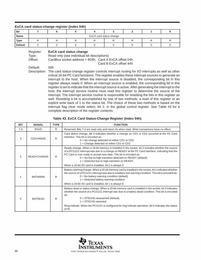
88 POST OFFICE BOX 655303 • DALLAS, TEXAS 75265
ExCA card status-change register (index 04h)Bit 7 6 5 4 3 2 1 0
Name ExCA card status change
Type R R R R R R R R
Default 0 0 0 0 0 0 0 0
Register: ExCA card status changeType: Read only (see individual bit descriptions)Offset: CardBus socket address + 804h; Card A ExCA offset 04h
Card B ExCA offset 44hDefault: 00hDescription: The card status-change register controls interrupt routing for I/O interrupts as well as other
critical 16-bit PC Card functions. The register enables these interrupt sources to generate aninterrupt to the host. When the interrupt source is disabled, the corresponding bit in thisregister always reads 0. When an interrupt source is enabled, the corresponding bit in thisregister is set to indicate that the interrupt source is active. After generating the interrupt to thehost, the interrupt service routine must read this register to determine the source of theinterrupt. The interrupt service routine is responsible for resetting the bits in this register aswell. Resetting a bit is accomplished by one of two methods: a read of this register or anexplicit write back of 1 to the status bit. The choice of these two methods is based on theinterrupt flag clear mode select, bit 2, in the global control register. See Table 43 for acomplete description of the register contents.
Table 43. ExCA Card Status-Change Register (Index 04h)
BIT SIGNAL TYPE FUNCTION
7-4 RSVD R Reserved. Bits 7-4 are read only and return 0s when read. Write transactions have no effect.
3 CDCHANGE R
Card detect change. Bit 3 indicates whether a change on CD1 or CD2 occurred at the PC Cardinterface. This bit is encoded as:
0 = No change detected on either CD1 or CD21 = Change detected on either CD1 or CD2
2 READYCHANGE R
Ready change. When a 16-bit memory is installed in the socket, bit 2 includes whether the sourceof a PCI1221 interrupt was due to a change on READY at the PC Card interface, indicating that thePC Card is now ready to accept new data. This bit is encoded as:
0 = No low-to-high transition detected on READY (default)1 = Detected low-to-high transition on READY
When a 16-bit I/O card is installed, bit 2 is always 0.
1 BATWARN R
Battery warning change. When a 16-bit memory card is installed in the socket, bit 1 indicates whetherthe source of a PCI1221 interrupt was due to a battery-low warning condition. This bit is encoded as:
0 = No battery warning condition (default)1 = Detected battery warning condition
When a 16-bit I/O card is installed, bit 1 is always 0.
0 BATDEAD R
Battery dead or status change. When a 16-bit memory card is installed in the socket, bit 0 indicateswhether the source of a PCI1221 interrupt was due to a battery dead condition. This bit is encodedas:
0 = STSCHG deasserted (default)1 = STSCHG asserted
Ring indicate. When the PCI1221 is configured for ring indicate operation, bit 0 indicates the statusof RI.
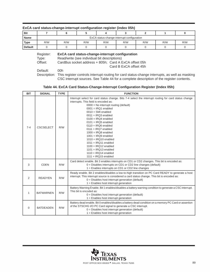
89POST OFFICE BOX 655303 • DALLAS, TEXAS 75265
ExCA card status-change-interrupt configuration register (index 05h)Bit 7 6 5 4 3 2 1 0
Name ExCA status-change-interrupt configuration
Type R/W R/W R/W R/W R/W R/W R/W R/W
Default 0 0 0 0 0 0 0 0
Register: ExCA card status-change-interrupt configurationType: Read/write (see individual bit descriptions)Offset: CardBus socket address + 805h; Card A ExCA offset 05h
Card B ExCA offset 45hDefault: 00hDescription: This register controls interrupt routing for card status-change interrupts, as well as masking
CSC interrupt sources. See Table 44 for a complete description of the register contents.
Table 44. ExCA Card Status-Change-Interrupt Configuration Register (Index 05h)
BIT SIGNAL TYPE FUNCTION
7-4 CSCSELECT R/W
Interrupt select for card status change. Bits 7-4 select the interrupt routing for card status changeinterrupts. This field is encoded as:
0000 = No interrupt routing (default)0001 = IRQ1 enabled0010 = SMI enabled0011 = IRQ3 enabled0100 = IRQ4 enabled0101 = IRQ5 enabled0110 = IRQ6 enabled0111 = IRQ7 enabled1000 = IRQ8 enabled1001 = IRQ9 enabled1010 = IRQ10 enabled1011 = IRQ11 enabled1100 = IRQ12 enabled1101 = IRQ13 enabled1110 = IRQ14 enabled1111 = IRQ15 enabled
3 CDEN R/WCard detect enable. Bit 3 enables interrupts on CD1 or CD2 changes. This bit is encoded as:
0 = Disables interrupts on CD1 or CD2 line changes (default)1 = Enables interrupts on CD1 or CD2 line changes
2 READYEN R/W
Ready enable. Bit 2 enables/disables a low-to-high transition on PC Card READY to generate a hostinterrupt. This interrupt source is considered a card status change. This bit is encoded as:
0 = Disables host interrupt generation (default)1 = Enables host interrupt generation
1 BATWARNEN R/W
Battery Warning Enable. Bit 1 enables/disables a battery warning condition to generate a CSC interrupt.This bit is encoded as:
0 = Disables host interrupt generation (default)1 = Enables host interrupt generation
0 BATDEADEN R/W
Battery dead enable. Bit 0 enables/disables a battery dead condition on a memory PC Card or assertionof the STSCHG I/O PC Card signal to generate a CSC interrupt.
0 = Disables host interrupt generation (default)1 = Enables host interrupt generation
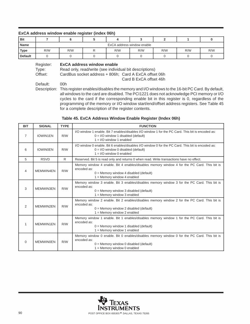
90 POST OFFICE BOX 655303 • DALLAS, TEXAS 75265
ExCA address window enable register (index 06h)Bit 7 6 5 4 3 2 1 0
Name ExCA address window enable
Type R/W R/W R R/W R/W R/W R/W R/W
Default 0 0 0 0 0 0 0 0
Register: ExCA address window enableType: Read only, read/write (see individual bit descriptions)Offset: CardBus socket address + 806h; Card A ExCA offset 06h
Card B ExCA offset 46hDefault: 00hDescription: This register enables/disables the memory and I/O windows to the 16-bit PC Card. By default,
all windows to the card are disabled. The PCI1221 does not acknowledge PCI memory or I/Ocycles to the card if the corresponding enable bit in this register is 0, regardless of theprogramming of the memory or I/O window start/end/offset address registers. See Table 45for a complete description of the register contents.
Table 45. ExCA Address Window Enable Register (Index 06h)
BIT SIGNAL TYPE FUNCTION
7 IOWIN1EN R/WI/O window 1 enable. Bit 7 enables/disables I/O window 1 for the PC Card. This bit is encoded as:
0 = I/O window 1 disabled (default)1 = I/O window 1 enabled
6 IOWIN0EN R/WI/O window 0 enable. Bit 6 enables/disables I/O window 0 for the PC Card. This bit is encoded as:
0 = I/O window 0 disabled (default)1 = I/O window 0 enabled
5 RSVD R Reserved. Bit 5 is read only and returns 0 when read. Write transactions have no effect.
4 MEMWIN4EN R/W
Memory window 4 enable. Bit 4 enables/disables memory window 4 for the PC Card. This bit isencoded as:
0 = Memory window 4 disabled (default)1 = Memory window 4 enabled
3 MEMWIN3EN R/W
Memory window 3 enable. Bit 3 enables/disables memory window 3 for the PC Card. This bit isencoded as:
0 = Memory window 3 disabled (default)1 = Memory window 3 enabled
2 MEMWIN2EN R/W
Memory window 2 enable. Bit 2 enables/disables memory window 2 for the PC Card. This bit isencoded as:
0 = Memory window 2 disabled (default)1 = Memory window 2 enabled
1 MEMWIN1EN R/W
Memory window 1 enable. Bit 1 enables/disables memory window 1 for the PC Card. This bit isencoded as:
0 = Memory window 1 disabled (default)1 = Memory window 1 enabled
0 MEMWIN0EN R/W
Memory window 0 enable. Bit 0 enables/disables memory window 0 for the PC Card. This bit isencoded as:
0 = Memory window 0 disabled (default)1 = Memory window 0 enabled
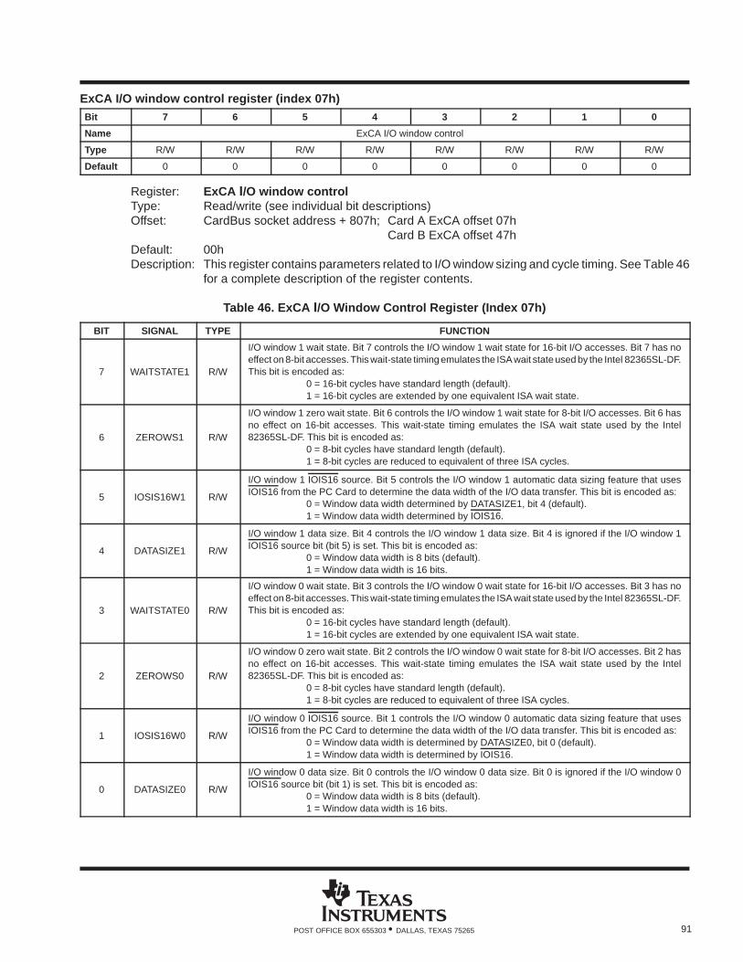
91POST OFFICE BOX 655303 • DALLAS, TEXAS 75265
ExCA I/O window control register (index 07h)Bit 7 6 5 4 3 2 1 0
Name ExCA I/O window control
Type R/W R/W R/W R/W R/W R/W R/W R/W
Default 0 0 0 0 0 0 0 0
Register: ExCA I/O window controlType: Read/write (see individual bit descriptions)Offset: CardBus socket address + 807h; Card A ExCA offset 07h
Card B ExCA offset 47hDefault: 00hDescription: This register contains parameters related to I/O window sizing and cycle timing. See Table 46
for a complete description of the register contents.
Table 46. ExCA I/O Window Control Register (Index 07h)
BIT SIGNAL TYPE FUNCTION
7 WAITSTATE1 R/W
I/O window 1 wait state. Bit 7 controls the I/O window 1 wait state for 16-bit I/O accesses. Bit 7 has noeffect on 8-bit accesses. This wait-state timing emulates the ISA wait state used by the Intel 82365SL-DF.This bit is encoded as:
0 = 16-bit cycles have standard length (default).1 = 16-bit cycles are extended by one equivalent ISA wait state.
6 ZEROWS1 R/W
I/O window 1 zero wait state. Bit 6 controls the I/O window 1 wait state for 8-bit I/O accesses. Bit 6 hasno effect on 16-bit accesses. This wait-state timing emulates the ISA wait state used by the Intel82365SL-DF. This bit is encoded as:
0 = 8-bit cycles have standard length (default).1 = 8-bit cycles are reduced to equivalent of three ISA cycles.
5 IOSIS16W1 R/W
I/O window 1 IOIS16 source. Bit 5 controls the I/O window 1 automatic data sizing feature that usesIOIS16 from the PC Card to determine the data width of the I/O data transfer. This bit is encoded as:
0 = Window data width determined by DATASIZE1, bit 4 (default).1 = Window data width determined by IOIS16.
4 DATASIZE1 R/W
I/O window 1 data size. Bit 4 controls the I/O window 1 data size. Bit 4 is ignored if the I/O window 1IOIS16 source bit (bit 5) is set. This bit is encoded as:
0 = Window data width is 8 bits (default).1 = Window data width is 16 bits.
3 WAITSTATE0 R/W
I/O window 0 wait state. Bit 3 controls the I/O window 0 wait state for 16-bit I/O accesses. Bit 3 has noeffect on 8-bit accesses. This wait-state timing emulates the ISA wait state used by the Intel 82365SL-DF.This bit is encoded as:
0 = 16-bit cycles have standard length (default).1 = 16-bit cycles are extended by one equivalent ISA wait state.
2 ZEROWS0 R/W
I/O window 0 zero wait state. Bit 2 controls the I/O window 0 wait state for 8-bit I/O accesses. Bit 2 hasno effect on 16-bit accesses. This wait-state timing emulates the ISA wait state used by the Intel82365SL-DF. This bit is encoded as:
0 = 8-bit cycles have standard length (default).1 = 8-bit cycles are reduced to equivalent of three ISA cycles.
1 IOSIS16W0 R/W
I/O window 0 IOIS16 source. Bit 1 controls the I/O window 0 automatic data sizing feature that usesIOIS16 from the PC Card to determine the data width of the I/O data transfer. This bit is encoded as:
0 = Window data width is determined by DATASIZE0, bit 0 (default).1 = Window data width is determined by IOIS16.
0 DATASIZE0 R/W
I/O window 0 data size. Bit 0 controls the I/O window 0 data size. Bit 0 is ignored if the I/O window 0IOIS16 source bit (bit 1) is set. This bit is encoded as:
0 = Window data width is 8 bits (default).1 = Window data width is 16 bits.
92 POST OFFICE BOX 655303 • DALLAS, TEXAS 75265
ExCA I/O window 0 and 1 start-address low-byte register (index 08h, 0Ch)Bit 7 6 5 4 3 2 1 0
Name ExCA I/O window 0 and 1 start-address low byte
Type R/W R/W R/W R/W R/W R/W R/W R/W
Default 0 0 0 0 0 0 0 0
Register: ExCA I/O window 0 start-address low byteOffset: CardBus socket address + 808h; Card A ExCA offset 08h
Card B ExCA offset 48hRegister: ExCA I/O window 1 start-address low byteOffset: CardBus socket address + 80Ch; Card A ExCA offset 0Ch
Card B ExCA offset 4ChType: Read/writeDefault: 00hSize: One byteDescription: These registers contain the low byte of the 16-bit I/O window start address for I/O windows 0
and 1. The eight bits of these registers correspond to the lower eight bits of the start address.
ExCA I/O window 0 and 1 start-address high-byte register (index 09h, 0Dh)Bit 7 6 5 4 3 2 1 0
Name ExCA I/O window 0 and 1 start-address high byte
Type R/W R/W R/W R/W R/W R/W R/W R/W
Default 0 0 0 0 0 0 0 0
Register: ExCA I/O window 0 start-address high byteOffset: CardBus socket address + 809h; Card A ExCA offset 09h
Card B ExCA offset 49hRegister: ExCA I/O window 1 start-address high byteOffset: CardBus socket address + 80Dh; Card A ExCA offset 0Dh
Card B ExCA offset 4DhType: Read/writeDefault: 00hSize: One byteDescription: These registers contain the high byte of the 16-bit I/O window start address for I/O windows 0
and 1. The eight bits of these registers correspond to the upper eight bits of the end address.
93POST OFFICE BOX 655303 • DALLAS, TEXAS 75265
ExCA I/O window 0 and 1 end-address low-byte register (index 0Ah, 0Eh)Bit 7 6 5 4 3 2 1 0
Name ExCA I/O window 0 and 1 end-address low byte
Type R/W R/W R/W R/W R/W R/W R/W R/W
Default 0 0 0 0 0 0 0 0
Register: ExCA I/O window 0 end-address low byteOffset: CardBus socket address + 80Ah; Card A ExCA offset 0Ah
Card B ExCA offset 4AhRegister: ExCA I/O window 1 end-address low byteOffset: CardBus socket address + 80Eh; Card A ExCA offset 0Eh
Card B ExCA offset 4EhType: Read/writeDefault: 00hSize: One byteDescription: These registers contain the low byte of the 16-bit I/O window end address for I/O windows 0
and 1. The eight bits of these registers correspond to the lower eight bits of the end address.
ExCA I/O window 0 and 1 end-address high-byte register (index 0Bh, 0Fh)Bit 7 6 5 4 3 2 1 0
Name ExCA I/O window 0 and 1 end-address high byte
Type R/W R/W R/W R/W R/W R/W R/W R/W
Default 0 0 0 0 0 0 0 0
Register: ExCA I/O window 0 end-address high byteOffset: CardBus socket address + 80Bh; Card A ExCA offset 0Bh
Card B ExCA offset 4BhRegister: ExCA I/O window 1 end-address high byteOffset: CardBus socket address + 80Fh; Card A ExCA offset 0Fh
Card B ExCA offset 4FhType: Read/writeDefault: 00hSize: One byteDescription: These registers contain the high byte of the 16-bit I/O window end address for I/O windows 0
and 1. The eight bits of these registers correspond to the upper eight bits of the end address.

94 POST OFFICE BOX 655303 • DALLAS, TEXAS 75265
ExCA memory window 0–4 start-address low-byte register (index 10h, 18h, 20h, 28h, 30h)Bit 7 6 5 4 3 2 1 0
Name ExCA memory window 0–4 start-address low byte
Type R/W R/W R/W R/W R/W R/W R/W R/W
Default 0 0 0 0 0 0 0 0
Register: ExCA memory window 0 start-address low byteOffset: CardBus socket address + 810h; Card A ExCA offset 10h
Card B ExCA offset 50hRegister: ExCA memory window 1 start-address low byteOffset: CardBus socket address + 818h; Card A ExCA offset 18h
Card B ExCA offset 58hRegister: ExCA memory window 2 start-address low byteOffset: CardBus socket address + 820h; Card A ExCA offset 20h
Card B ExCA offset 60h
Register: ExCA memory window 3 start-address low byteOffset: CardBus socket address + 828h; Card A ExCA offset 28h
Card B ExCA offset 68hRegister: ExCA memory window 4 start-address low byteOffset: CardBus socket address + 830h; Card A ExCA offset 30h
Card B ExCA offset 70hType: Read/writeDefault: 00hSize: One byteDescription: These registers contain the low byte of the 16-bit memory window start address for memory
windows 0, 1, 2, 3, and 4. The eight bits of these registers correspond to bits A19–A12 of thestart address.
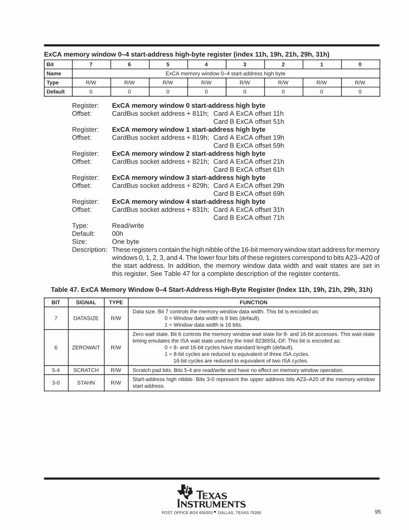
95POST OFFICE BOX 655303 • DALLAS, TEXAS 75265
ExCA memory window 0–4 start-address high-byte register (index 11h, 19h, 21h, 29h, 31h)Bit 7 6 5 4 3 2 1 0
Name ExCA memory window 0–4 start-address high byte
Type R/W R/W R/W R/W R/W R/W R/W R/W
Default 0 0 0 0 0 0 0 0
Register: ExCA memory window 0 start-address high byteOffset: CardBus socket address + 811h; Card A ExCA offset 11h
Card B ExCA offset 51hRegister: ExCA memory window 1 start-address high byteOffset: CardBus socket address + 819h; Card A ExCA offset 19h
Card B ExCA offset 59hRegister: ExCA memory window 2 start-address high byteOffset: CardBus socket address + 821h; Card A ExCA offset 21h
Card B ExCA offset 61hRegister: ExCA memory window 3 start-address high byteOffset: CardBus socket address + 829h; Card A ExCA offset 29h
Card B ExCA offset 69hRegister: ExCA memory window 4 start-address high byteOffset: CardBus socket address + 831h; Card A ExCA offset 31h
Card B ExCA offset 71hType: Read/writeDefault: 00hSize: One byteDescription: These registers contain the high nibble of the 16-bit memory window start address for memory
windows 0, 1, 2, 3, and 4. The lower four bits of these registers correspond to bits A23–A20 ofthe start address. In addition, the memory window data width and wait states are set inthis register. See Table 47 for a complete description of the register contents.
Table 47. ExCA Memory Window 0–4 Start-Address High-Byte Register (Index 11h, 19h, 21h, 29h, 31h)
BIT SIGNAL TYPE FUNCTION
7 DATASIZE R/WData size. Bit 7 controls the memory window data width. This bit is encoded as:
0 = Window data width is 8 bits (default).1 = Window data width is 16 bits.
6 ZEROWAIT R/W
Zero wait state. Bit 6 controls the memory window wait state for 8- and 16-bit accesses. This wait-statetiming emulates the ISA wait state used by the Intel 82365SL-DF. This bit is encoded as:
0 = 8- and 16-bit cycles have standard length (default).1 = 8-bit cycles are reduced to equivalent of three ISA cycles.
16-bit cycles are reduced to equivalent of two ISA cycles.
5-4 SCRATCH R/W Scratch pad bits. Bits 5-4 are read/write and have no effect on memory window operation.
3-0 STAHN R/WStart-address high nibble. Bits 3-0 represent the upper address bits A23–A20 of the memory windowstart address.
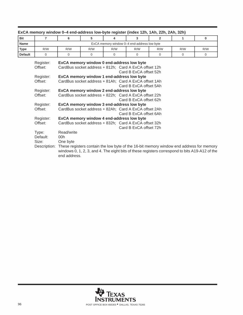
96 POST OFFICE BOX 655303 • DALLAS, TEXAS 75265
ExCA memory window 0–4 end-address low-byte register (index 12h, 1Ah, 22h, 2Ah, 32h)Bit 7 6 5 4 3 2 1 0
Name ExCA memory window 0–4 end-address low byte
Type R/W R/W R/W R/W R/W R/W R/W R/W
Default 0 0 0 0 0 0 0 0
Register: ExCA memory window 0 end-address low byteOffset: CardBus socket address + 812h; Card A ExCA offset 12h
Card B ExCA offset 52hRegister: ExCA memory window 1 end-address low byteOffset: CardBus socket address + 81Ah; Card A ExCA offset 1Ah
Card B ExCA offset 5AhRegister: ExCA memory window 2 end-address low byteOffset: CardBus socket address + 822h; Card A ExCA offset 22h
Card B ExCA offset 62hRegister: ExCA memory window 3 end-address low byteOffset: CardBus socket address + 82Ah; Card A ExCA offset 2Ah
Card B ExCA offset 6AhRegister: ExCA memory window 4 end-address low byteOffset: CardBus socket address + 832h; Card A ExCA offset 32h
Card B ExCA offset 72hType: Read/writeDefault: 00hSize: One byteDescription: These registers contain the low byte of the 16-bit memory window end address for memory
windows 0, 1, 2, 3, and 4. The eight bits of these registers correspond to bits A19-A12 of theend address.
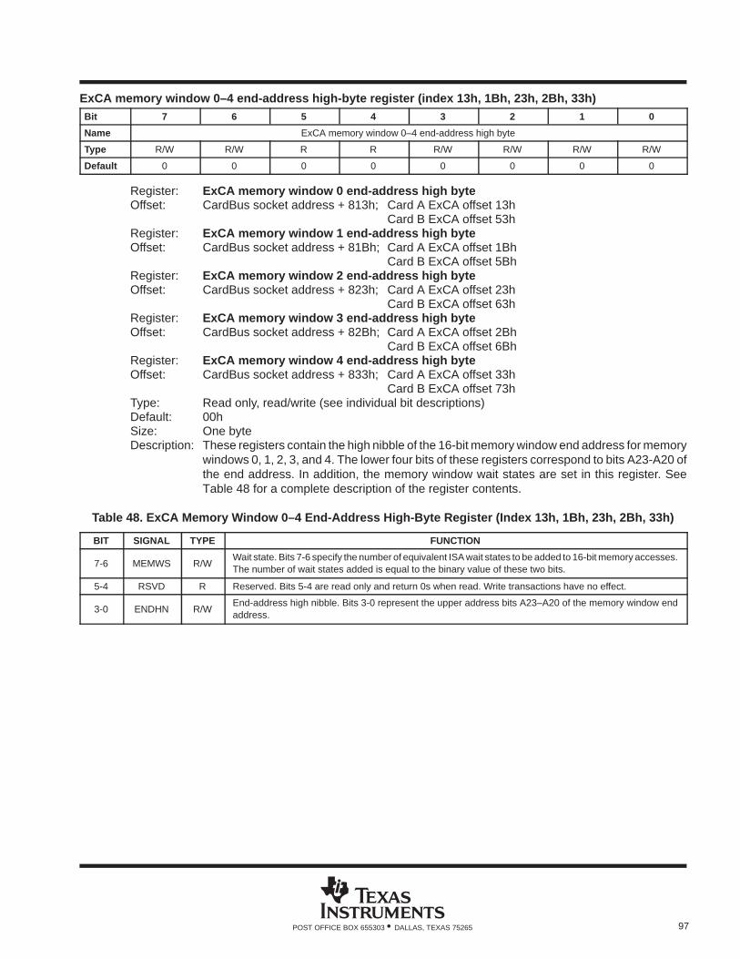
97POST OFFICE BOX 655303 • DALLAS, TEXAS 75265
ExCA memory window 0–4 end-address high-byte register (index 13h, 1Bh, 23h, 2Bh, 33h)Bit 7 6 5 4 3 2 1 0
Name ExCA memory window 0–4 end-address high byte
Type R/W R/W R R R/W R/W R/W R/W
Default 0 0 0 0 0 0 0 0
Register: ExCA memory window 0 end-address high byteOffset: CardBus socket address + 813h; Card A ExCA offset 13h
Card B ExCA offset 53hRegister: ExCA memory window 1 end-address high byteOffset: CardBus socket address + 81Bh; Card A ExCA offset 1Bh
Card B ExCA offset 5BhRegister: ExCA memory window 2 end-address high byteOffset: CardBus socket address + 823h; Card A ExCA offset 23h
Card B ExCA offset 63hRegister: ExCA memory window 3 end-address high byteOffset: CardBus socket address + 82Bh; Card A ExCA offset 2Bh
Card B ExCA offset 6BhRegister: ExCA memory window 4 end-address high byteOffset: CardBus socket address + 833h; Card A ExCA offset 33h
Card B ExCA offset 73hType: Read only, read/write (see individual bit descriptions)Default: 00hSize: One byteDescription: These registers contain the high nibble of the 16-bit memory window end address for memory
windows 0, 1, 2, 3, and 4. The lower four bits of these registers correspond to bits A23-A20 ofthe end address. In addition, the memory window wait states are set in this register. SeeTable 48 for a complete description of the register contents.
Table 48. ExCA Memory Window 0–4 End-Address High-Byte Register (Index 13h, 1Bh, 23h, 2Bh, 33h)
BIT SIGNAL TYPE FUNCTION
7-6 MEMWS R/WWait state. Bits 7-6 specify the number of equivalent ISA wait states to be added to 16-bit memory accesses.The number of wait states added is equal to the binary value of these two bits.
5-4 RSVD R Reserved. Bits 5-4 are read only and return 0s when read. Write transactions have no effect.
3-0 ENDHN R/WEnd-address high nibble. Bits 3-0 represent the upper address bits A23–A20 of the memory window endaddress.
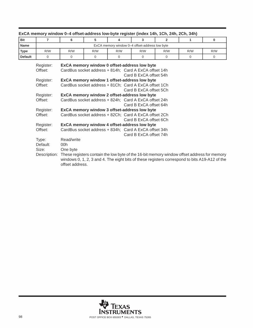
98 POST OFFICE BOX 655303 • DALLAS, TEXAS 75265
ExCA memory window 0–4 offset-address low-byte register (index 14h, 1Ch, 24h, 2Ch, 34h)Bit 7 6 5 4 3 2 1 0
Name ExCA memory window 0–4 offset-address low byte
Type R/W R/W R/W R/W R/W R/W R/W R/W
Default 0 0 0 0 0 0 0 0
Register: ExCA memory window 0 offset-address low byteOffset: CardBus socket address + 814h; Card A ExCA offset 14h
Card B ExCA offset 54hRegister: ExCA memory window 1 offset-address low byteOffset: CardBus socket address + 81Ch; Card A ExCA offset 1Ch
Card B ExCA offset 5ChRegister: ExCA memory window 2 offset-address low byteOffset: CardBus socket address + 824h; Card A ExCA offset 24h
Card B ExCA offset 64hRegister: ExCA memory window 3 offset-address low byteOffset: CardBus socket address + 82Ch; Card A ExCA offset 2Ch
Card B ExCA offset 6ChRegister: ExCA memory window 4 offset-address low byteOffset: CardBus socket address + 834h; Card A ExCA offset 34h
Card B ExCA offset 74hType: Read/writeDefault: 00hSize: One byteDescription: These registers contain the low byte of the 16-bit memory window offset address for memory
windows 0, 1, 2, 3 and 4. The eight bits of these registers correspond to bits A19-A12 of theoffset address.
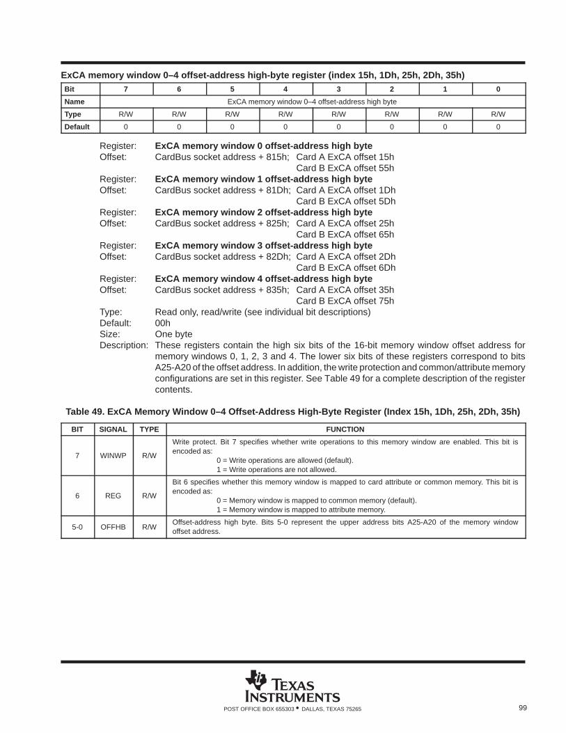
99POST OFFICE BOX 655303 • DALLAS, TEXAS 75265
ExCA memory window 0–4 offset-address high-byte register (index 15h, 1Dh, 25h, 2Dh, 35h)Bit 7 6 5 4 3 2 1 0
Name ExCA memory window 0–4 offset-address high byte
Type R/W R/W R/W R/W R/W R/W R/W R/W
Default 0 0 0 0 0 0 0 0
Register: ExCA memory window 0 offset-address high byteOffset: CardBus socket address + 815h; Card A ExCA offset 15h
Card B ExCA offset 55hRegister: ExCA memory window 1 offset-address high byteOffset: CardBus socket address + 81Dh; Card A ExCA offset 1Dh
Card B ExCA offset 5DhRegister: ExCA memory window 2 offset-address high byteOffset: CardBus socket address + 825h; Card A ExCA offset 25h
Card B ExCA offset 65hRegister: ExCA memory window 3 offset-address high byteOffset: CardBus socket address + 82Dh; Card A ExCA offset 2Dh
Card B ExCA offset 6DhRegister: ExCA memory window 4 offset-address high byteOffset: CardBus socket address + 835h; Card A ExCA offset 35h
Card B ExCA offset 75hType: Read only, read/write (see individual bit descriptions)Default: 00hSize: One byteDescription: These registers contain the high six bits of the 16-bit memory window offset address for
memory windows 0, 1, 2, 3 and 4. The lower six bits of these registers correspond to bitsA25-A20 of the offset address. In addition, the write protection and common/attribute memoryconfigurations are set in this register. See Table 49 for a complete description of the registercontents.
Table 49. ExCA Memory Window 0–4 Offset-Address High-Byte Register (Index 15h, 1Dh, 25h, 2Dh, 35h)
BIT SIGNAL TYPE FUNCTION
7 WINWP R/W
Write protect. Bit 7 specifies whether write operations to this memory window are enabled. This bit isencoded as:
0 = Write operations are allowed (default).1 = Write operations are not allowed.
6 REG R/W
Bit 6 specifies whether this memory window is mapped to card attribute or common memory. This bit isencoded as:
0 = Memory window is mapped to common memory (default).1 = Memory window is mapped to attribute memory.
5-0 OFFHB R/WOffset-address high byte. Bits 5-0 represent the upper address bits A25-A20 of the memory windowoffset address.
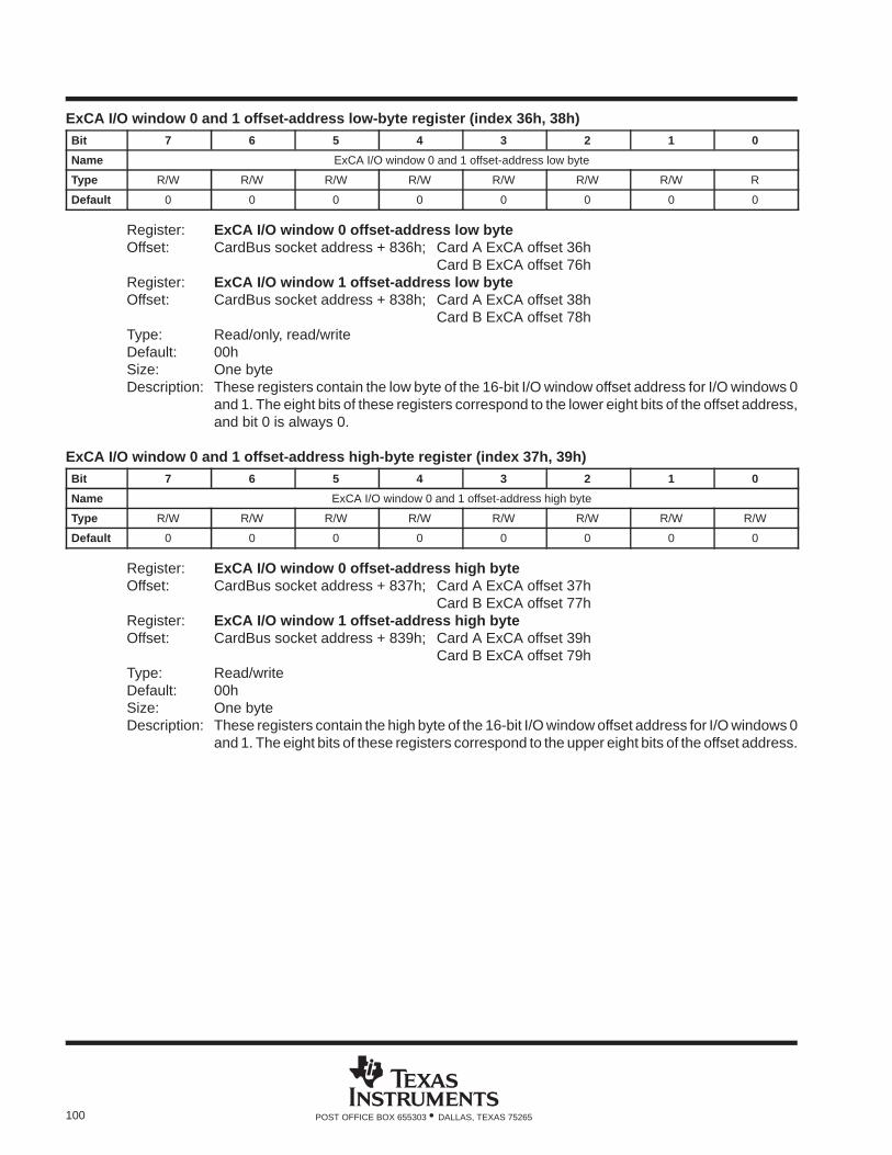
100 POST OFFICE BOX 655303 • DALLAS, TEXAS 75265
ExCA I/O window 0 and 1 offset-address low-byte register (index 36h, 38h)Bit 7 6 5 4 3 2 1 0
Name ExCA I/O window 0 and 1 offset-address low byte
Type R/W R/W R/W R/W R/W R/W R/W R
Default 0 0 0 0 0 0 0 0
Register: ExCA I/O window 0 offset-address low byteOffset: CardBus socket address + 836h; Card A ExCA offset 36h
Card B ExCA offset 76hRegister: ExCA I/O window 1 offset-address low byteOffset: CardBus socket address + 838h; Card A ExCA offset 38h
Card B ExCA offset 78hType: Read/only, read/writeDefault: 00hSize: One byteDescription: These registers contain the low byte of the 16-bit I/O window offset address for I/O windows 0
and 1. The eight bits of these registers correspond to the lower eight bits of the offset address,and bit 0 is always 0.
ExCA I/O window 0 and 1 offset-address high-byte register (index 37h, 39h)Bit 7 6 5 4 3 2 1 0
Name ExCA I/O window 0 and 1 offset-address high byte
Type R/W R/W R/W R/W R/W R/W R/W R/W
Default 0 0 0 0 0 0 0 0
Register: ExCA I/O window 0 offset-address high byteOffset: CardBus socket address + 837h; Card A ExCA offset 37h
Card B ExCA offset 77hRegister: ExCA I/O window 1 offset-address high byteOffset: CardBus socket address + 839h; Card A ExCA offset 39h
Card B ExCA offset 79hType: Read/writeDefault: 00hSize: One byteDescription: These registers contain the high byte of the 16-bit I/O window offset address for I/O windows 0
and 1. The eight bits of these registers correspond to the upper eight bits of the offset address.
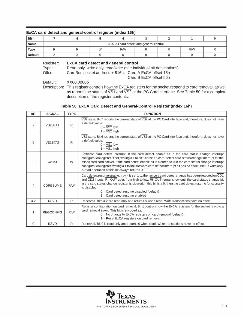
101POST OFFICE BOX 655303 • DALLAS, TEXAS 75265
ExCA card detect and general-control register (index 16h)Bit 7 6 5 4 3 2 1 0
Name ExCA I/O card detect and general control
Type R R W R/W R R R/W R
Default X X 0 0 0 0 0 0
Register: ExCA card detect and general controlType: Read only, write only, read/write (see individual bit descriptions)Offset: CardBus socket address + 816h; Card A ExCA offset 16h
Card B ExCA offset 56hDefault: XX00 0000bDescription: This register controls how the ExCA registers for the socket respond to card removal, as well
as reports the status of VS1 and VS2 at the PC Card interface. See Table 50 for a completedescription of the register contents.
Table 50. ExCA Card Detect and General-Control Register (Index 16h)
BIT SIGNAL TYPE FUNCTION
7 VS2STAT R
VS2 state. Bit 7 reports the current state of VS2 at the PC Card interface and, therefore, does not havea default value.
0 = VS2 low1 = VS2 high
6 VS1STAT R
VS1 state. Bit 6 reports the current state of VS1 at the PC Card interface and, therefore, does not havea default value.
0 = VS1 low1 = VS1 high
5 SWCSC W
Software card detect interrupt. If the card detect enable bit in the card status change interruptconfiguration register is set, writing a 1 to bit 5 causes a card-detect card-status change interrupt for theassociated card socket. If the card detect enable bit is cleared to 0 in the card status change interruptconfiguration register, writing a 1 to the software card detect interrupt bit has no effect. Bit 5 is write only.A read operation of this bit always returns 0.
4 CDRESUME R/W
Card detect resume enable. If bit 4 is set to 1, then once a card detect change has been detected on CD1and CD2 inputs, RI_OUT goes from high to low. RI_OUT remains low until the card status change bitin the card status change register is cleared. If this bit is a 0, then the card detect resume functionalityis disabled.
0 = Card detect resume disabled (default)1 = Card detect resume enabled
3-2 RSVD R Reserved. Bits 3-2 are read only and return 0s when read. Write transactions have no effect.
1 REGCONFIG R/W
Register configuration on card removal. Bit 1 controls how the ExCA registers for the socket react to acard removal event. This bit is encoded as:
0 = No change to ExCA registers on card removal (default)1 = Reset ExCA registers on card removal
0 RSVD R Reserved. Bit 0 is read only and returns 0 when read. Write transactions have no effect.
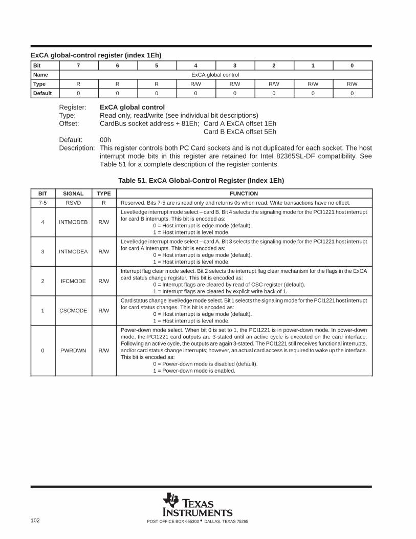
102 POST OFFICE BOX 655303 • DALLAS, TEXAS 75265
ExCA global-control register (index 1Eh)Bit 7 6 5 4 3 2 1 0
Name ExCA global control
Type R R R R/W R/W R/W R/W R/W
Default 0 0 0 0 0 0 0 0
Register: ExCA global controlType: Read only, read/write (see individual bit descriptions)Offset: CardBus socket address + 81Eh; Card A ExCA offset 1Eh
Card B ExCA offset 5EhDefault: 00hDescription: This register controls both PC Card sockets and is not duplicated for each socket. The host
interrupt mode bits in this register are retained for Intel 82365SL-DF compatibility. SeeTable 51 for a complete description of the register contents.
Table 51. ExCA Global-Control Register (Index 1Eh)
BIT SIGNAL TYPE FUNCTION
7-5 RSVD R Reserved. Bits 7-5 are is read only and returns 0s when read. Write transactions have no effect.
4 INTMODEB R/W
Level/edge interrupt mode select – card B. Bit 4 selects the signaling mode for the PCI1221 host interruptfor card B interrupts. This bit is encoded as:
0 = Host interrupt is edge mode (default).1 = Host interrupt is level mode.
3 INTMODEA R/W
Level/edge interrupt mode select – card A. Bit 3 selects the signaling mode for the PCI1221 host interruptfor card A interrupts. This bit is encoded as:
0 = Host interrupt is edge mode (default).1 = Host interrupt is level mode.
2 IFCMODE R/W
Interrupt flag clear mode select. Bit 2 selects the interrupt flag clear mechanism for the flags in the ExCAcard status change register. This bit is encoded as:
0 = Interrupt flags are cleared by read of CSC register (default).1 = Interrupt flags are cleared by explicit write back of 1.
1 CSCMODE R/W
Card status change level/edge mode select. Bit 1 selects the signaling mode for the PCI1221 host interruptfor card status changes. This bit is encoded as:
0 = Host interrupt is edge mode (default).1 = Host interrupt is level mode.
0 PWRDWN R/W
Power-down mode select. When bit 0 is set to 1, the PCI1221 is in power-down mode. In power-downmode, the PCI1221 card outputs are 3-stated until an active cycle is executed on the card interface.Following an active cycle, the outputs are again 3-stated. The PCI1221 still receives functional interrupts,and/or card status change interrupts; however, an actual card access is required to wake up the interface.This bit is encoded as:
0 = Power-down mode is disabled (default).1 = Power-down mode is enabled.
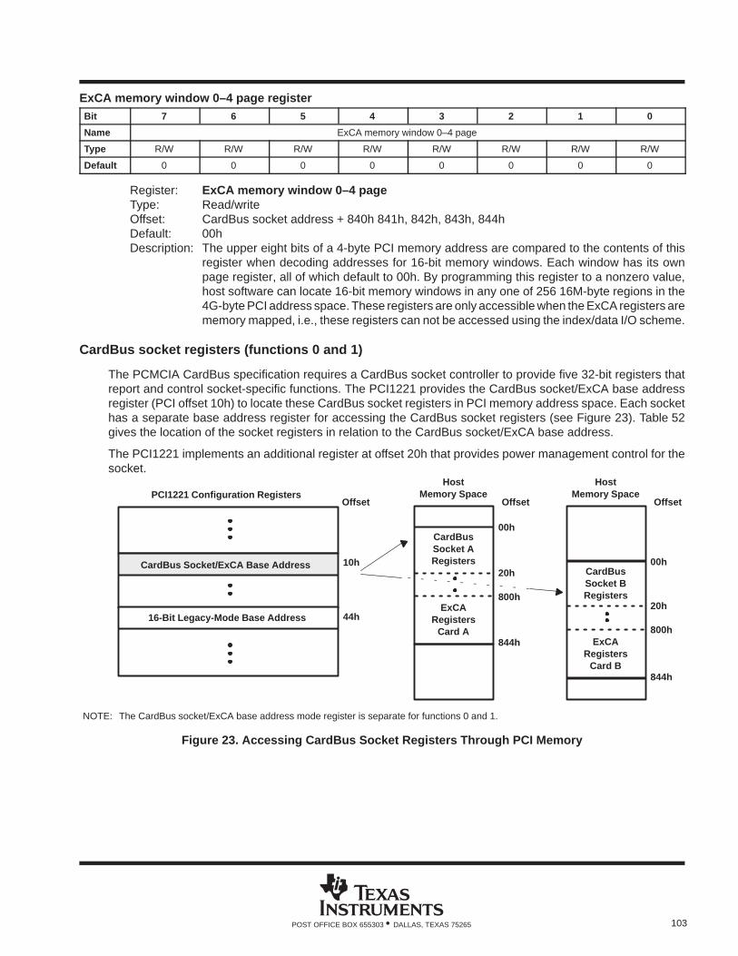
103POST OFFICE BOX 655303 • DALLAS, TEXAS 75265
ExCA memory window 0–4 page registerBit 7 6 5 4 3 2 1 0
Name ExCA memory window 0–4 page
Type R/W R/W R/W R/W R/W R/W R/W R/W
Default 0 0 0 0 0 0 0 0
Register: ExCA memory window 0–4 pageType: Read/writeOffset: CardBus socket address + 840h 841h, 842h, 843h, 844hDefault: 00hDescription: The upper eight bits of a 4-byte PCI memory address are compared to the contents of this
register when decoding addresses for 16-bit memory windows. Each window has its ownpage register, all of which default to 00h. By programming this register to a nonzero value,host software can locate 16-bit memory windows in any one of 256 16M-byte regions in the4G-byte PCI address space. These registers are only accessible when the ExCA registers arememory mapped, i.e., these registers can not be accessed using the index/data I/O scheme.
CardBus socket registers (functions 0 and 1)
The PCMCIA CardBus specification requires a CardBus socket controller to provide five 32-bit registers thatreport and control socket-specific functions. The PCI1221 provides the CardBus socket/ExCA base addressregister (PCI offset 10h) to locate these CardBus socket registers in PCI memory address space. Each sockethas a separate base address register for accessing the CardBus socket registers (see Figure 23). Table 52gives the location of the socket registers in relation to the CardBus socket/ExCA base address.
The PCI1221 implements an additional register at offset 20h that provides power management control for thesocket.
CardBus Socket/ExCA Base Address
16-Bit Legacy-Mode Base Address
10h
44h
NOTE: The CardBus socket/ExCA base address mode register is separate for functions 0 and 1.
PCI1221 Configuration Registers
CardBusSocket ARegisters
HostMemory Space
00h
ExCARegisters
Card A
20h
800h
844h
Offset
CardBusSocket BRegisters
HostMemory Space
00h
ExCARegisters
Card B
20h
800h
844h
OffsetOffset
Figure 23. Accessing CardBus Socket Registers Through PCI Memory
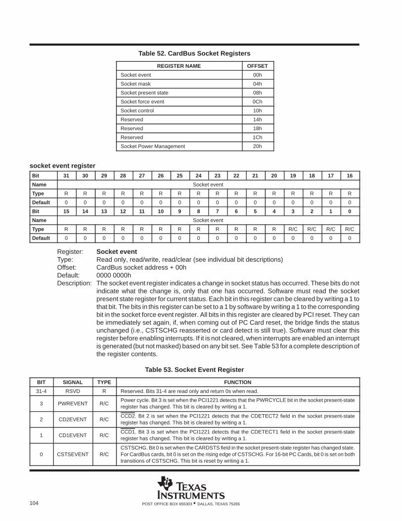
104 POST OFFICE BOX 655303 • DALLAS, TEXAS 75265
Table 52. CardBus Socket Registers
REGISTER NAME OFFSET
Socket event 00h
Socket mask 04h
Socket present state 08h
Socket force event 0Ch
Socket control 10h
Reserved 14h
Reserved 18h
Reserved 1Ch
Socket Power Management 20h
socket event registerBit 31 30 29 28 27 26 25 24 23 22 21 20 19 18 17 16
Name Socket event
Type R R R R R R R R R R R R R R R R
Default 0 0 0 0 0 0 0 0 0 0 0 0 0 0 0 0
Bit 15 14 13 12 11 10 9 8 7 6 5 4 3 2 1 0
Name Socket event
Type R R R R R R R R R R R R R/C R/C R/C R/C
Default 0 0 0 0 0 0 0 0 0 0 0 0 0 0 0 0
Register: Socket eventType: Read only, read/write, read/clear (see individual bit descriptions)Offset: CardBus socket address + 00hDefault: 0000 0000hDescription: The socket event register indicates a change in socket status has occurred. These bits do not
indicate what the change is, only that one has occurred. Software must read the socketpresent state register for current status. Each bit in this register can be cleared by writing a 1 tothat bit. The bits in this register can be set to a 1 by software by writing a 1 to the correspondingbit in the socket force event register. All bits in this register are cleared by PCI reset. They canbe immediately set again, if, when coming out of PC Card reset, the bridge finds the statusunchanged (i.e., CSTSCHG reasserted or card detect is still true). Software must clear thisregister before enabling interrupts. If it is not cleared, when interrupts are enabled an interruptis generated (but not masked) based on any bit set. See Table 53 for a complete description ofthe register contents.
Table 53. Socket Event Register
BIT SIGNAL TYPE FUNCTION
31-4 RSVD R Reserved. Bits 31-4 are read only and return 0s when read.
3 PWREVENT R/CPower cycle. Bit 3 is set when the PCI1221 detects that the PWRCYCLE bit in the socket present-stateregister has changed. This bit is cleared by writing a 1.
2 CD2EVENT R/CCCD2. Bit 2 is set when the PCI1221 detects that the CDETECT2 field in the socket present-stateregister has changed. This bit is cleared by writing a 1.
1 CD1EVENT R/CCCD1. Bit 3 is set when the PCI1221 detects that the CDETECT1 field in the socket present-stateregister has changed. This bit is cleared by writing a 1.
0 CSTSEVENT R/CCSTSCHG. Bit 0 is set when the CARDSTS field in the socket present-state register has changed state.For CardBus cards, bit 0 is set on the rising edge of CSTSCHG. For 16-bit PC Cards, bit 0 is set on bothtransitions of CSTSCHG. This bit is reset by writing a 1.
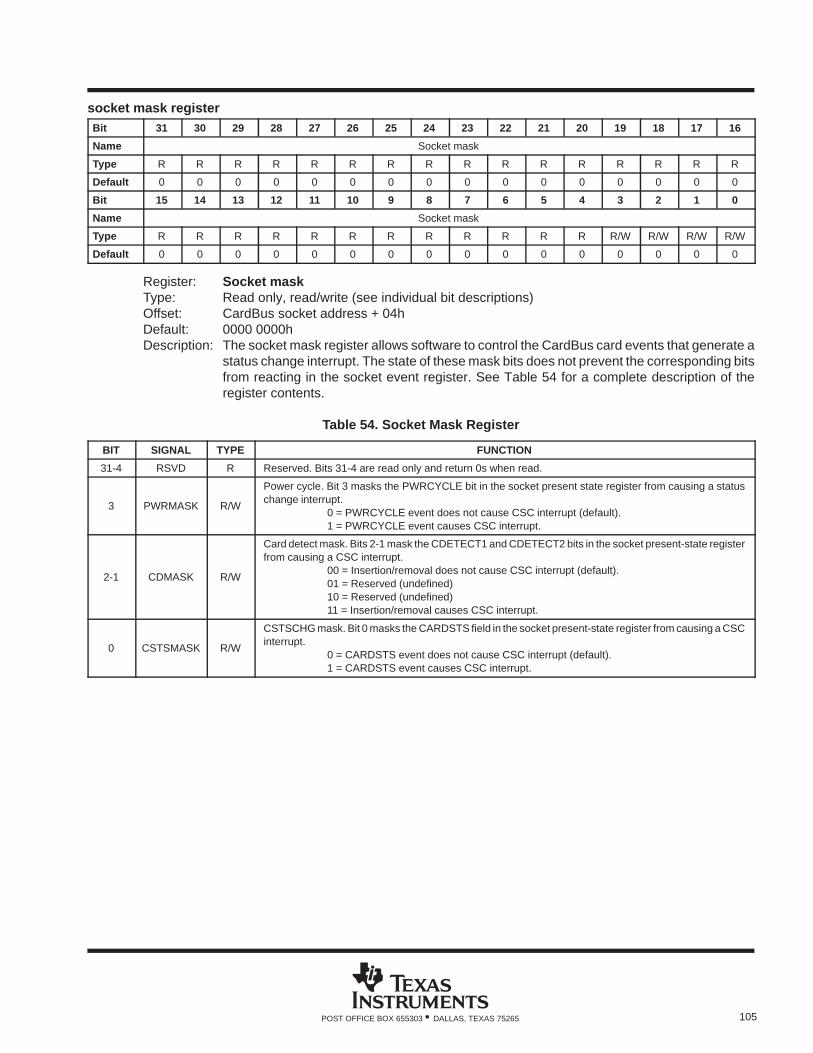
105POST OFFICE BOX 655303 • DALLAS, TEXAS 75265
socket mask registerBit 31 30 29 28 27 26 25 24 23 22 21 20 19 18 17 16
Name Socket mask
Type R R R R R R R R R R R R R R R R
Default 0 0 0 0 0 0 0 0 0 0 0 0 0 0 0 0
Bit 15 14 13 12 11 10 9 8 7 6 5 4 3 2 1 0
Name Socket mask
Type R R R R R R R R R R R R R/W R/W R/W R/W
Default 0 0 0 0 0 0 0 0 0 0 0 0 0 0 0 0
Register: Socket maskType: Read only, read/write (see individual bit descriptions)Offset: CardBus socket address + 04hDefault: 0000 0000hDescription: The socket mask register allows software to control the CardBus card events that generate a
status change interrupt. The state of these mask bits does not prevent the corresponding bitsfrom reacting in the socket event register. See Table 54 for a complete description of theregister contents.
Table 54. Socket Mask Register
BIT SIGNAL TYPE FUNCTION
31-4 RSVD R Reserved. Bits 31-4 are read only and return 0s when read.
3 PWRMASK R/W
Power cycle. Bit 3 masks the PWRCYCLE bit in the socket present state register from causing a statuschange interrupt.
0 = PWRCYCLE event does not cause CSC interrupt (default).1 = PWRCYCLE event causes CSC interrupt.
2-1 CDMASK R/W
Card detect mask. Bits 2-1 mask the CDETECT1 and CDETECT2 bits in the socket present-state registerfrom causing a CSC interrupt.
00 = Insertion/removal does not cause CSC interrupt (default).01 = Reserved (undefined)10 = Reserved (undefined)11 = Insertion/removal causes CSC interrupt.
0 CSTSMASK R/W
CSTSCHG mask. Bit 0 masks the CARDSTS field in the socket present-state register from causing a CSCinterrupt.
0 = CARDSTS event does not cause CSC interrupt (default).1 = CARDSTS event causes CSC interrupt.
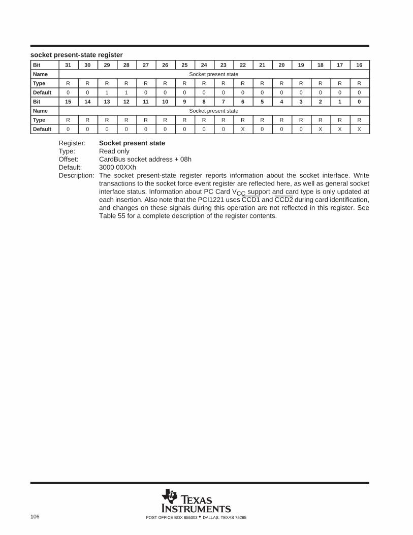
106 POST OFFICE BOX 655303 • DALLAS, TEXAS 75265
socket present-state registerBit 31 30 29 28 27 26 25 24 23 22 21 20 19 18 17 16
Name Socket present state
Type R R R R R R R R R R R R R R R R
Default 0 0 1 1 0 0 0 0 0 0 0 0 0 0 0 0
Bit 15 14 13 12 11 10 9 8 7 6 5 4 3 2 1 0
Name Socket present state
Type R R R R R R R R R R R R R R R R
Default 0 0 0 0 0 0 0 0 0 X 0 0 0 X X X
Register: Socket present stateType: Read onlyOffset: CardBus socket address + 08hDefault: 3000 00XXhDescription: The socket present-state register reports information about the socket interface. Write
transactions to the socket force event register are reflected here, as well as general socketinterface status. Information about PC Card VCC support and card type is only updated ateach insertion. Also note that the PCI1221 uses CCD1 and CCD2 during card identification,and changes on these signals during this operation are not reflected in this register. SeeTable 55 for a complete description of the register contents.
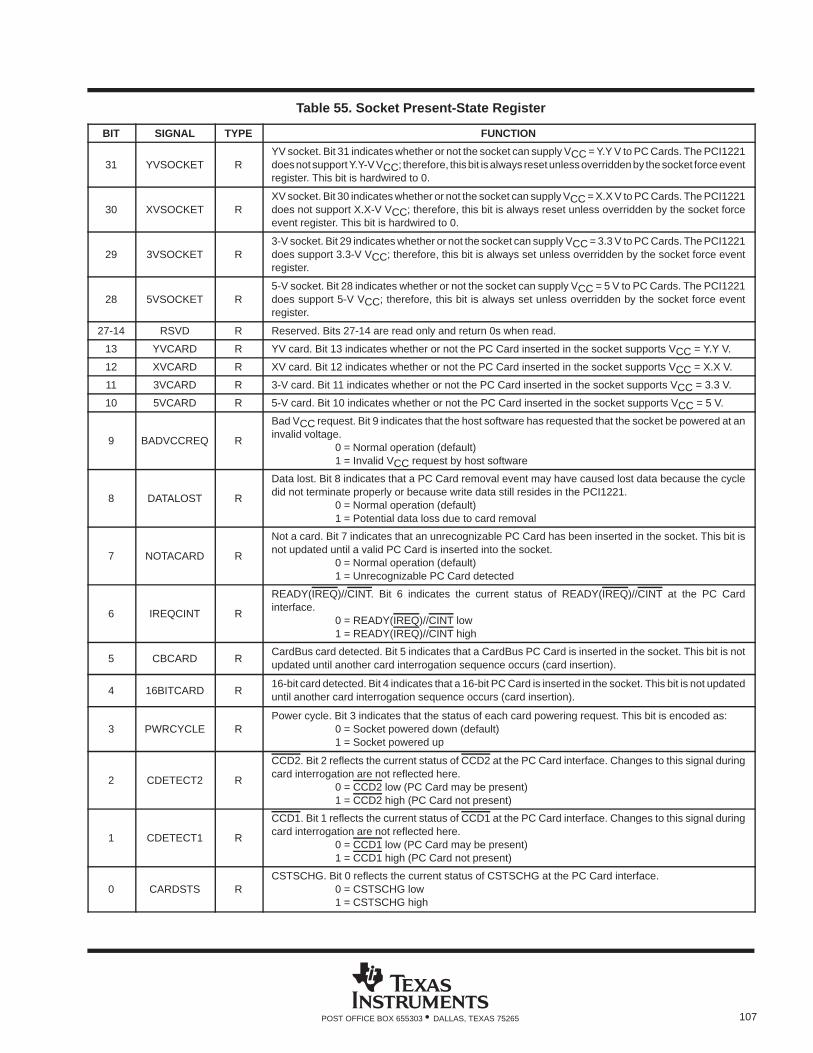
107POST OFFICE BOX 655303 • DALLAS, TEXAS 75265
Table 55. Socket Present-State Register
BIT SIGNAL TYPE FUNCTION
31 YVSOCKET RYV socket. Bit 31 indicates whether or not the socket can supply VCC = Y.Y V to PC Cards. The PCI1221does not support Y.Y-V VCC; therefore, this bit is always reset unless overridden by the socket force eventregister. This bit is hardwired to 0.
30 XVSOCKET RXV socket. Bit 30 indicates whether or not the socket can supply VCC = X.X V to PC Cards. The PCI1221does not support X.X-V VCC; therefore, this bit is always reset unless overridden by the socket forceevent register. This bit is hardwired to 0.
29 3VSOCKET R3-V socket. Bit 29 indicates whether or not the socket can supply VCC = 3.3 V to PC Cards. The PCI1221does support 3.3-V VCC; therefore, this bit is always set unless overridden by the socket force eventregister.
28 5VSOCKET R5-V socket. Bit 28 indicates whether or not the socket can supply VCC = 5 V to PC Cards. The PCI1221does support 5-V VCC; therefore, this bit is always set unless overridden by the socket force eventregister.
27-14 RSVD R Reserved. Bits 27-14 are read only and return 0s when read.
13 YVCARD R YV card. Bit 13 indicates whether or not the PC Card inserted in the socket supports VCC = Y.Y V.
12 XVCARD R XV card. Bit 12 indicates whether or not the PC Card inserted in the socket supports VCC = X.X V.
11 3VCARD R 3-V card. Bit 11 indicates whether or not the PC Card inserted in the socket supports VCC = 3.3 V.
10 5VCARD R 5-V card. Bit 10 indicates whether or not the PC Card inserted in the socket supports VCC = 5 V.
9 BADVCCREQ R
Bad VCC request. Bit 9 indicates that the host software has requested that the socket be powered at aninvalid voltage.
0 = Normal operation (default)1 = Invalid VCC request by host software
8 DATALOST R
Data lost. Bit 8 indicates that a PC Card removal event may have caused lost data because the cycledid not terminate properly or because write data still resides in the PCI1221.
0 = Normal operation (default)1 = Potential data loss due to card removal
7 NOTACARD R
Not a card. Bit 7 indicates that an unrecognizable PC Card has been inserted in the socket. This bit isnot updated until a valid PC Card is inserted into the socket.
0 = Normal operation (default)1 = Unrecognizable PC Card detected
6 IREQCINT R
READY(IREQ)//CINT. Bit 6 indicates the current status of READY(IREQ)//CINT at the PC Cardinterface.
0 = READY(IREQ)//CINT low1 = READY(IREQ)//CINT high
5 CBCARD RCardBus card detected. Bit 5 indicates that a CardBus PC Card is inserted in the socket. This bit is notupdated until another card interrogation sequence occurs (card insertion).
4 16BITCARD R16-bit card detected. Bit 4 indicates that a 16-bit PC Card is inserted in the socket. This bit is not updateduntil another card interrogation sequence occurs (card insertion).
3 PWRCYCLE RPower cycle. Bit 3 indicates that the status of each card powering request. This bit is encoded as:
0 = Socket powered down (default)1 = Socket powered up
2 CDETECT2 R
CCD2. Bit 2 reflects the current status of CCD2 at the PC Card interface. Changes to this signal duringcard interrogation are not reflected here.
0 = CCD2 low (PC Card may be present)1 = CCD2 high (PC Card not present)
1 CDETECT1 R
CCD1. Bit 1 reflects the current status of CCD1 at the PC Card interface. Changes to this signal duringcard interrogation are not reflected here.
0 = CCD1 low (PC Card may be present)1 = CCD1 high (PC Card not present)
0 CARDSTS RCSTSCHG. Bit 0 reflects the current status of CSTSCHG at the PC Card interface.
0 = CSTSCHG low1 = CSTSCHG high
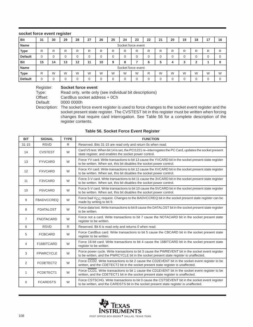
108 POST OFFICE BOX 655303 • DALLAS, TEXAS 75265
socket force event registerBit 31 30 29 28 27 26 25 24 23 22 21 20 19 18 17 16
Name Socket force event
Type R R R R R R R R R R R R R R R R
Default 0 0 0 0 0 0 0 0 0 0 0 0 0 0 0 0
Bit 15 14 13 12 11 10 9 8 7 6 5 4 3 2 1 0
Name Socket force event
Type R W W W W W W W W R W W W W W W
Default 0 0 0 0 0 0 0 0 0 0 0 0 0 0 0 0
Register: Socket force eventType: Read only, write only (see individual bit descriptions)Offset: CardBus socket address + 0ChDefault: 0000 0000hDescription: The socket force event register is used to force changes to the socket event register and the
socket present state register. The CVSTEST bit in this register must be written when forcingchanges that require card interrogation. See Table 56 for a complete description of theregister contents.
Table 56. Socket Force Event Register
BIT SIGNAL TYPE FUNCTION
31-15 RSVD R Reserved. Bits 31-15 are read only and return 0s when read.
14 CVSTEST WCard VS test. When bit 14 is set, the PCI1221 re–interrogates the PC Card, updates the socket presentstate register, and enables the socket power control.
13 FYVCARD WForce YV card. Write transactions to bit 13 cause the YVCARD bit in the socket present state registerto be written. When set, this bit disables the socket power control.
12 FXVCARD WForce XV card. Write transactions to bit 12 cause the XVCARD bit in the socket present state registerto be written. When set, this bit disables the socket power control.
11 F3VCARD WForce 3-V card. Write transactions to bit 11 cause the 3VCARD bit in the socket present state registerto be written. When set, this bit disables the socket power control.
10 F5VCARD WForce 5-V card. Write transactions to bit 10 cause the 5VCARD bit in the socket present state registerto be written. When set, this bit disables the socket power control.
9 FBADVCCREQ WForce bad VCC request. Changes to the BADVCCREQ bit in the socket present state register can bemade by writing to bit 9.
8 FDATALOST WForce data lost. Write transactions to bit 8 cause the DATALOST bit in the socket present state registerto be written.
7 FNOTACARD WForce not a card. Write transactions to bit 7 cause the NOTACARD bit in the socket present stateregister to be written.
6 RSVD R Reserved. Bit 6 is read only and returns 0 when read.
5 FCBCARD WForce CardBus card. Write transactions to bit 5 cause the CBCARD bit in the socket present stateregister to be written.
4 F16BITCARD WForce 16-bit card. Write transactions to bit 4 cause the 16BITCARD bit in the socket present stateregister to be written.
3 FPWRCYCLE WForce power cycle. Write transactions to bit 3 cause the PWREVENT bit in the socket event registerto be written, and the PWRCYCLE bit in the socket present state register is unaffected.
2 FCDETECT2 WForce CCD2. Write transactions to bit 2 cause the CD2EVENT bit in the socket event register to bewritten, and the CDETECT2 bit in the socket present state register is unaffected.
1 FCDETECT1 WForce CCD1. Write transactions to bit 1 cause the CD1EVENT bit in the socket event register to bewritten, and the CDETECT1 bit in the socket present state register is unaffected.
0 FCARDSTS WForce CSTSCHG. Write transactions to bit 0 cause the CSTSEVENT bit in the socket event registerto be written, and the CARDSTS bit in the socket present state register is unaffected.
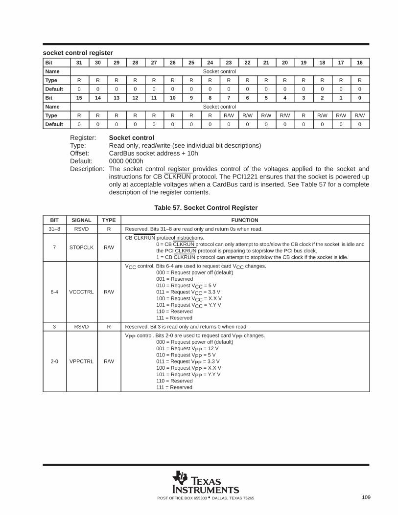
109POST OFFICE BOX 655303 • DALLAS, TEXAS 75265
socket control registerBit 31 30 29 28 27 26 25 24 23 22 21 20 19 18 17 16
Name Socket control
Type R R R R R R R R R R R R R R R R
Default 0 0 0 0 0 0 0 0 0 0 0 0 0 0 0 0
Bit 15 14 13 12 11 10 9 8 7 6 5 4 3 2 1 0
Name Socket control
Type R R R R R R R R R/W R/W R/W R/W R R/W R/W R/W
Default 0 0 0 0 0 0 0 0 0 0 0 0 0 0 0 0
Register: Socket controlType: Read only, read/write (see individual bit descriptions)Offset: CardBus socket address + 10hDefault: 0000 0000hDescription: The socket control register provides control of the voltages applied to the socket and
instructions for CB CLKRUN protocol. The PCI1221 ensures that the socket is powered uponly at acceptable voltages when a CardBus card is inserted. See Table 57 for a completedescription of the register contents.
Table 57. Socket Control Register
BIT SIGNAL TYPE FUNCTION
31–8 RSVD R Reserved. Bits 31–8 are read only and return 0s when read.
7 STOPCLK R/W
CB CLKRUN protocol instructions.0 = CB CLKRUN protocol can only attempt to stop/slow the CB clock if the socket is idle andthe PCI CLKRUN protocol is preparing to stop/slow the PCI bus clock.1 = CB CLKRUN protocol can attempt to stop/slow the CB clock if the socket is idle.
6-4 VCCCTRL R/W
VCC control. Bits 6-4 are used to request card VCC changes.000 = Request power off (default)001 = Reserved010 = Request VCC = 5 V011 = Request VCC = 3.3 V100 = Request VCC = X.X V101 = Request VCC = Y.Y V110 = Reserved111 = Reserved
3 RSVD R Reserved. Bit 3 is read only and returns 0 when read.
2-0 VPPCTRL R/W
VPP control. Bits 2-0 are used to request card VPP changes.000 = Request power off (default)001 = Request VPP = 12 V010 = Request VPP = 5 V011 = Request VPP = 3.3 V100 = Request VPP = X.X V101 = Request VPP = Y.Y V110 = Reserved111 = Reserved
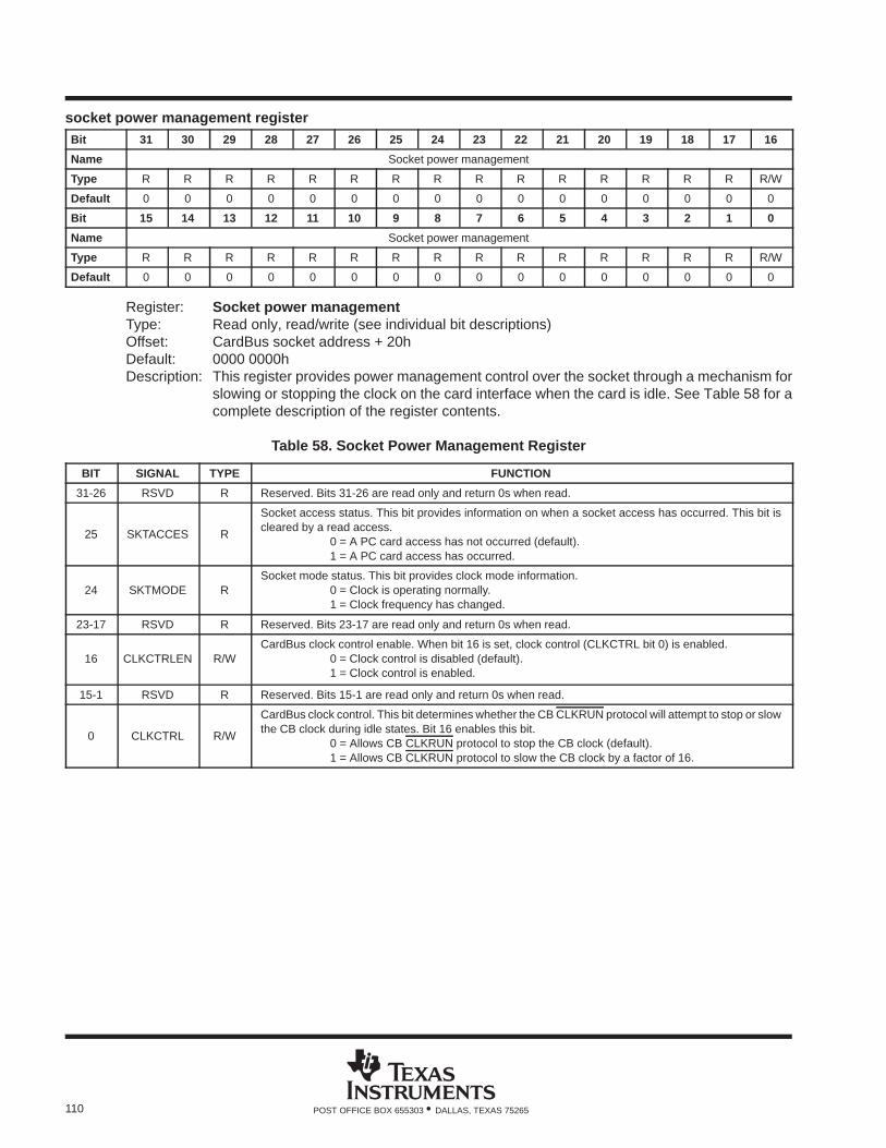
110 POST OFFICE BOX 655303 • DALLAS, TEXAS 75265
socket power management registerBit 31 30 29 28 27 26 25 24 23 22 21 20 19 18 17 16
Name Socket power management
Type R R R R R R R R R R R R R R R R/W
Default 0 0 0 0 0 0 0 0 0 0 0 0 0 0 0 0
Bit 15 14 13 12 11 10 9 8 7 6 5 4 3 2 1 0
Name Socket power management
Type R R R R R R R R R R R R R R R R/W
Default 0 0 0 0 0 0 0 0 0 0 0 0 0 0 0 0
Register: Socket power managementType: Read only, read/write (see individual bit descriptions)Offset: CardBus socket address + 20hDefault: 0000 0000hDescription: This register provides power management control over the socket through a mechanism for
slowing or stopping the clock on the card interface when the card is idle. See Table 58 for acomplete description of the register contents.
Table 58. Socket Power Management Register
BIT SIGNAL TYPE FUNCTION
31-26 RSVD R Reserved. Bits 31-26 are read only and return 0s when read.
25 SKTACCES R
Socket access status. This bit provides information on when a socket access has occurred. This bit iscleared by a read access.
0 = A PC card access has not occurred (default).1 = A PC card access has occurred.
24 SKTMODE RSocket mode status. This bit provides clock mode information.
0 = Clock is operating normally.1 = Clock frequency has changed.
23-17 RSVD R Reserved. Bits 23-17 are read only and return 0s when read.
16 CLKCTRLEN R/WCardBus clock control enable. When bit 16 is set, clock control (CLKCTRL bit 0) is enabled.
0 = Clock control is disabled (default).1 = Clock control is enabled.
15-1 RSVD R Reserved. Bits 15-1 are read only and return 0s when read.
0 CLKCTRL R/W
CardBus clock control. This bit determines whether the CB CLKRUN protocol will attempt to stop or slowthe CB clock during idle states. Bit 16 enables this bit.
0 = Allows CB CLKRUN protocol to stop the CB clock (default).1 = Allows CB CLKRUN protocol to slow the CB clock by a factor of 16.
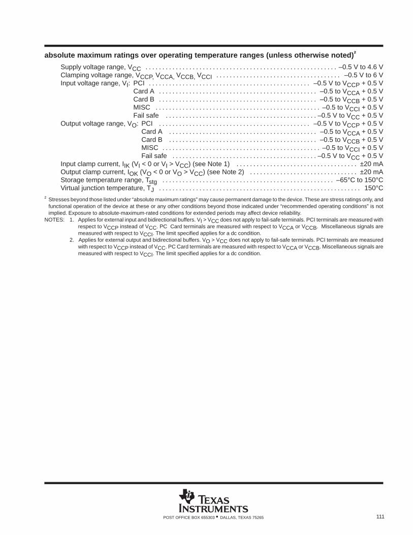
111POST OFFICE BOX 655303 • DALLAS, TEXAS 75265
absolute maximum ratings over operating temperature ranges (unless otherwise noted) †
Supply voltage range, VCC –0.5 V to 4.6 V. . . . . . . . . . . . . . . . . . . . . . . . . . . . . . . . . . . . . . . . . . . . . . . . . . . . . . . . . Clamping voltage range, VCCP, VCCA, VCCB, VCCI –0.5 V to 6 V. . . . . . . . . . . . . . . . . . . . . . . . . . . . . . . . . . . . . Input voltage range, VI: PCI –0.5 V to VCCP + 0.5 V. . . . . . . . . . . . . . . . . . . . . . . . . . . . . . . . . . . . . . . . . . . . . . . .
Card A –0.5 to VCCA + 0.5 V. . . . . . . . . . . . . . . . . . . . . . . . . . . . . . . . . . . . . . . . . . . . . . . Card B –0.5 to VCCB + 0.5 V. . . . . . . . . . . . . . . . . . . . . . . . . . . . . . . . . . . . . . . . . . . . . . . MISC –0.5 to VCCI + 0.5 V. . . . . . . . . . . . . . . . . . . . . . . . . . . . . . . . . . . . . . . . . . . . . . . . . Fail safe –0.5 V to VCC + 0.5 V. . . . . . . . . . . . . . . . . . . . . . . . . . . . . . . . . . . . . . . . . . . . .
Output voltage range, VO: PCI –0.5 V to VCCP + 0.5 V. . . . . . . . . . . . . . . . . . . . . . . . . . . . . . . . . . . . . . . . . . . . . Card A –0.5 to VCCA + 0.5 V. . . . . . . . . . . . . . . . . . . . . . . . . . . . . . . . . . . . . . . . . . . . Card B –0.5 to VCCB + 0.5 V. . . . . . . . . . . . . . . . . . . . . . . . . . . . . . . . . . . . . . . . . . . . MISC –0.5 to VCCI + 0.5 V. . . . . . . . . . . . . . . . . . . . . . . . . . . . . . . . . . . . . . . . . . . . . . . Fail safe –0.5 V to VCC + 0.5 V. . . . . . . . . . . . . . . . . . . . . . . . . . . . . . . . . . . . . . . . . . .
Input clamp current, IIK (VI < 0 or VI > VCC) (see Note 1) ±20 mA. . . . . . . . . . . . . . . . . . . . . . . . . . . . . . . . . . . . Output clamp current, IOK (VO < 0 or VO > VCC) (see Note 2) ±20 mA. . . . . . . . . . . . . . . . . . . . . . . . . . . . . . . . Storage temperature range, Tstg –65°C to 150°C. . . . . . . . . . . . . . . . . . . . . . . . . . . . . . . . . . . . . . . . . . . . . . . . . . . Virtual junction temperature, TJ 150°C. . . . . . . . . . . . . . . . . . . . . . . . . . . . . . . . . . . . . . . . . . . . . . . . . . . . . . . . . . . .
† Stresses beyond those listed under “absolute maximum ratings” may cause permanent damage to the device. These are stress ratings only, andfunctional operation of the device at these or any other conditions beyond those indicated under “recommended operating conditions” is notimplied. Exposure to absolute-maximum-rated conditions for extended periods may affect device reliability.
NOTES: 1. Applies for external input and bidirectional buffers. VI > VCC does not apply to fail-safe terminals. PCI terminals are measured withrespect to VCCP instead of VCC. PC Card terminals are measured with respect to VCCA or VCCB. Miscellaneous signals aremeasured with respect to VCCI. The limit specified applies for a dc condition.
2. Applies for external output and bidirectional buffers. VO > VCC does not apply to fail-safe terminals. PCI terminals are measuredwith respect to VCCP instead of VCC. PC Card terminals are measured with respect to VCCA or VCCB. Miscellaneous signals aremeasured with respect to VCCI. The limit specified applies for a dc condition.
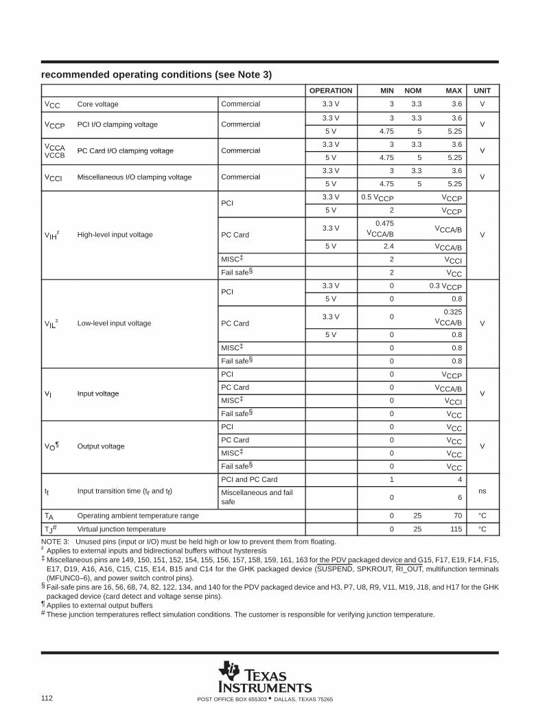
112 POST OFFICE BOX 655303 • DALLAS, TEXAS 75265
recommended operating conditions (see Note 3)
OPERATION MIN NOM MAX UNIT
VCC Core voltage Commercial 3.3 V 3 3.3 3.6 V
VCCP PCI I/O clamping voltage Commercial3.3 V 3 3.3 3.6
VVCCP PCI I/O clam ing voltage Commercial5 V 4.75 5 5.25
V
VCCA PC Card I/O clamping voltage Commercial3.3 V 3 3.3 3.6
VCCAVCCB
PC Card I/O clam ing voltage Commercial5 V 4.75 5 5.25
V
VCCI Miscellaneous I/O clamping voltage Commercial3.3 V 3 3.3 3.6
VVCCI Miscellaneous I/O clam ing voltage Commercial5 V 4.75 5 5.25
V
†
PCI3.3 V 0.5 VCCP VCCP
†
PCI5 V 2 VCCP
VIH† High-level input voltage PC Card3.3 V
0.475VCCA/B
VCCA/BVIH
5 V 2.4 VCCA/B
MISC‡ 2 VCCI
Fail safe§ 2 VCC
†
PCI3.3 V 0 0.3 VCCP
†
PCI5 V 0 0.8
VIL† Low-level input voltage PC Card3.3 V 0
0.325VCCA/B VIL
5 V 0 0.8
MISC‡ 0 0.8
Fail safe§ 0 0.8
PCI 0 VCCP
VI Input voltagePC Card 0 VCCA/B
VVI In ut voltageMISC‡ 0 VCCI
V
Fail safe§ 0 VCC
¶
PCI 0 VCC
VO¶ Output voltagePC Card 0 VCC
VVO¶ Out ut voltageMISC‡ 0 VCC
V
Fail safe§ 0 VCC
PCI and PC Card 1 4
tt Input transition time (tr and tf) Miscellaneous and failsafe
0 6ns
TA Operating ambient temperature range 0 25 70 °C
TJ# Virtual junction temperature 0 25 115 °C
NOTE 3: Unused pins (input or I/O) must be held high or low to prevent them from floating.† Applies to external inputs and bidirectional buffers without hysteresis‡ Miscellaneous pins are 149, 150, 151, 152, 154, 155, 156, 157, 158, 159, 161, 163 for the PDV packaged device and G15, F17, E19, F14, F15,
E17, D19, A16, A16, C15, C15, E14, B15 and C14 for the GHK packaged device (SUSPEND, SPKROUT, RI_OUT, multifunction terminals(MFUNC0–6), and power switch control pins).
§ Fail-safe pins are 16, 56, 68, 74, 82, 122, 134, and 140 for the PDV packaged device and H3, P7, U8, R9, V11, M19, J18, and H17 for the GHKpackaged device (card detect and voltage sense pins).
¶ Applies to external output buffers# These junction temperatures reflect simulation conditions. The customer is responsible for verifying junction temperature.
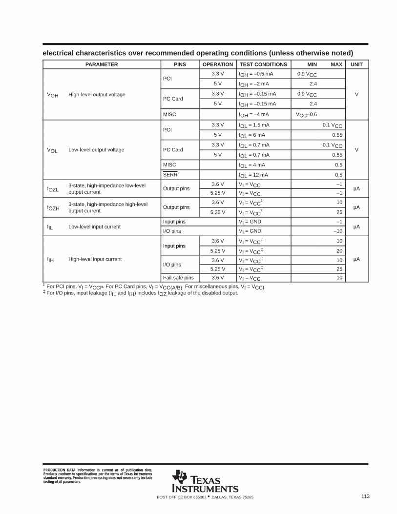
113POST OFFICE BOX 655303 • DALLAS, TEXAS 75265
electrical characteristics over recommended operating conditions (unless otherwise noted)
PARAMETER PINS OPERATION TEST CONDITIONS MIN MAX UNIT
PCI3.3 V IOH = –0.5 mA 0.9 VCC
PCI5 V IOH = –2 mA 2.4
VOH High-level output voltagePC Card
3.3 V IOH = –0.15 mA 0.9 VCC VPC Card
5 V IOH = –0.15 mA 2.4
MISC IOH = 4 mA VCC 0 6MISC IOH = –4 mA VCC–0.6
PCI3.3 V IOL = 1.5 mA 0.1 VCC
PCI5 V IOL = 6 mA 0.55
VOL Low level output voltage PC Card3.3 V IOL = 0.7 mA 0.1 VCC
VVOL Low-level output voltage PC Card5 V IOL = 0.7 mA 0.55
V
MISC IOL = 4 mA 0.5
SERR IOL = 12 mA 0.5
IOZL3-state, high-impedance low-level Output pins
3.6 V VI = VCC –1µAIOZL
, goutput current
Output pins5.25 V VI = VCC –1
µA
IOZH3-state, high-impedance high-level Output pins
3.6 V VI = VCC† 10µAIOZH
, g goutput current
Output pins5.25 V VI = VCC† 25
µA
I Lo le el inp t c rrentInput pins VI = GND –1
AIIL Low-level input currentI/O pins VI = GND –10
µA
Input pins3.6 V VI = VCC‡ 10
Input pins5.25 V VI = VCC‡ 20
IIH High-level input currentI/O pins
3.6 V VI = VCC‡ 10 µAI/O pins
5.25 V VI = VCC‡ 25
Fail-safe pins 3.6 V VI = VCC 10
† For PCI pins, VI = VCCP. For PC Card pins, VI = VCC(A/B). For miscellaneous pins, VI = VCCI‡ For I/O pins, input leakage (IIL and IIH) includes IOZ leakage of the disabled output.
PRODUCTION DATA information is current as of publication date.Products conform to specifications per the terms of Texas Instrumentsstandard warranty. Production processing does not necessarily includetesting of all parameters.
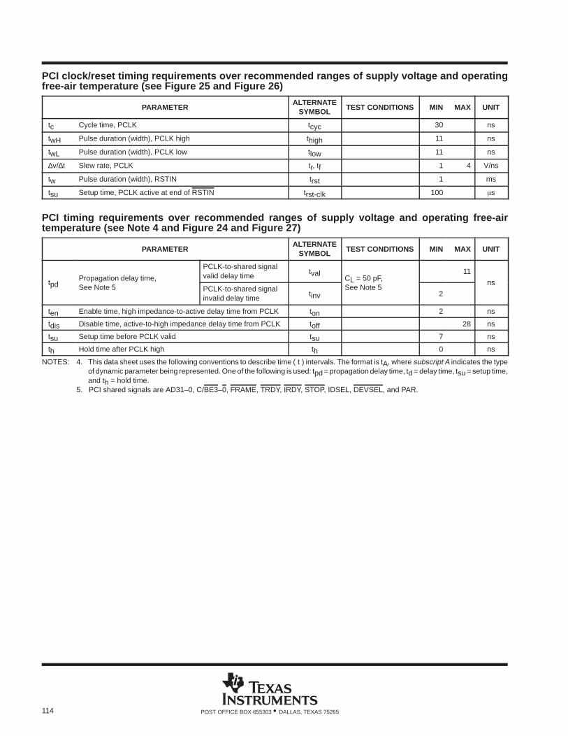
114 POST OFFICE BOX 655303 • DALLAS, TEXAS 75265
PCI clock/reset timing requirements over recommended ranges of supply voltage and operatingfree-air temperature (see Figure 25 and Figure 26)
PARAMETERALTERNATE
SYMBOL TEST CONDITIONS MIN MAX UNIT
tc Cycle time, PCLK tcyc 30 ns
twH Pulse duration (width), PCLK high thigh 11 ns
twL Pulse duration (width), PCLK low tlow 11 ns
∆v/∆t Slew rate, PCLK tr, tf 1 4 V/ns
tw Pulse duration (width), RSTIN trst 1 ms
tsu Setup time, PCLK active at end of RSTIN trst-clk 100 s
PCI timing requirements over recommended ranges of supply voltage and operating free-airtemperature (see Note 4 and Figure 24 and Figure 27)
PARAMETERALTERNATE
SYMBOL TEST CONDITIONS MIN MAX UNIT
t dPropagation delay time,
PCLK-to-shared signalvalid delay time
tvalCL = 50 pF,
11
nstpdg y ,
See Note 5 PCLK-to-shared signalinvalid delay time
tinv
L ,See Note 5
2
ns
ten Enable time, high impedance-to-active delay time from PCLK ton 2 ns
tdis Disable time, active-to-high impedance delay time from PCLK toff 28 ns
tsu Setup time before PCLK valid tsu 7 ns
th Hold time after PCLK high th 0 ns
NOTES: 4. This data sheet uses the following conventions to describe time ( t ) intervals. The format is tA, where subscript A indicates the typeof dynamic parameter being represented. One of the following is used: tpd = propagation delay time, td = delay time, tsu = setup time,and th = hold time.
5. PCI shared signals are AD31–0, C/BE3–0, FRAME, TRDY, IRDY, STOP, IDSEL, DEVSEL, and PAR.
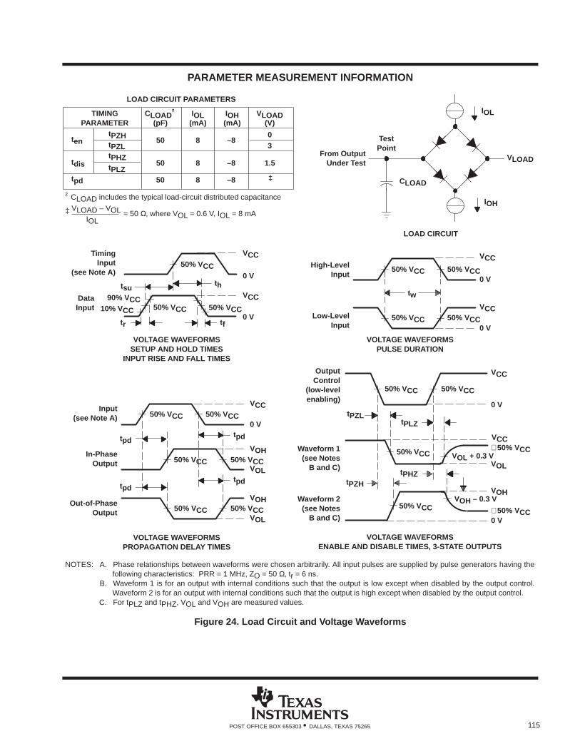
115POST OFFICE BOX 655303 • DALLAS, TEXAS 75265
PARAMETER MEASUREMENT INFORMATION
† CLOAD includes the typical load-circuit distributed capacitance
CLOAD
TestPoint
TimingInput
(see Note A)
Out-of-PhaseOutput
tpd
50% VCC
50% VCC
VCC
0 V
0 V
0 V
0 V
0 V
VOL
thtsu
VOH
VOH
VOL
High-LevelInput
Low-LevelInput
tw
VOLTAGE WAVEFORMSPROPAGATION DELAY TIMES
LOAD CIRCUIT
VOLTAGE WAVEFORMSSETUP AND HOLD TIMES
INPUT RISE AND FALL TIMES
VOLTAGE WAVEFORMSPULSE DURATION
tpdtpd
tpd
VLOAD
IOH
IOL
From Output Under Test
90% VCC10% VCC
tftr
OutputControl
(low-levelenabling)
Waveform 1(see Notes
B and C)
Waveform 2(see Notes
B and C)
VOL
VOHVOH – 0.3 V
tPZL
tPZH
tPLZ
tPHZ
VOLTAGE WAVEFORMSENABLE AND DISABLE TIMES, 3-STATE OUTPUTS
VOL + 0.3 V
0 V
0 V
≅ 50% VCC
≅ 50% VCC
ten
tdis
tpd
tPZHtPZLtPHZtPLZ
CLOAD†
(pF)IOL
(mA)TIMING
PARAMETER
50 8 –8
03
1.5
‡50 8
8
–8
–8
LOAD CIRCUIT PARAMETERS
= 50 Ω, where VOL = 0.6 V, IOL = 8 mAIOL
50
‡ VLOAD – VOL
IOH(mA)
VLOAD(V)
DataInput
In-PhaseOutput
Input(see Note A)
VCC
VCC
VCC50% VCC
50% VCC 50% VCC
50% VCC
VCC
VCC
50% VCC 50% VCC
50% VCC
50% VCC
VCC50% VCC 50% VCC
50% VCC 50% VCC
50% VCC 50% VCC
NOTES: A. Phase relationships between waveforms were chosen arbitrarily. All input pulses are supplied by pulse generators having thefollowing characteristics: PRR = 1 MHz, ZO = 50 Ω, tr = 6 ns.
B. Waveform 1 is for an output with internal conditions such that the output is low except when disabled by the output control.Waveform 2 is for an output with internal conditions such that the output is high except when disabled by the output control.
C. For tPLZ and tPHZ, VOL and VOH are measured values.
50% VCC
Figure 24. Load Circuit and Voltage Waveforms
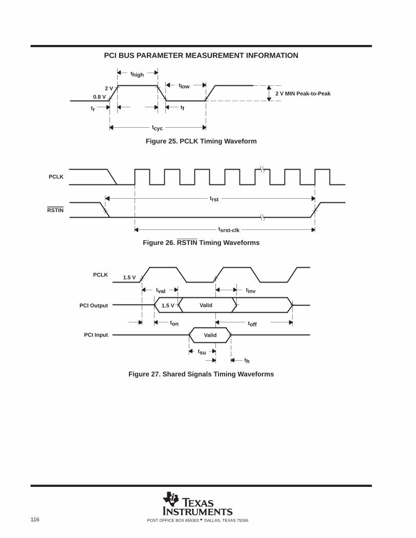
116 POST OFFICE BOX 655303 • DALLAS, TEXAS 75265
PCI BUS PARAMETER MEASUREMENT INFORMATION
thigh
2 V
0.8 V
tr tf
tcyc
tlow2 V MIN Peak-to-Peak
Figure 25. PCLK Timing Waveform
trst
tsrst-clk
PCLK
RSTIN
Figure 26. RSTIN Timing Waveforms
1.5 V
tval tinv
Valid1.5 V
ton toff
Valid
tsuth
PCLK
PCI Output
PCI Input
Figure 27. Shared Signals Timing Waveforms
117POST OFFICE BOX 655303 • DALLAS, TEXAS 75265
PC Card cycle timing
The PC Card cycle timing is controlled by the wait-state bits in the Intel 82365SL-DF compatible memory andI/O window registers. The PC Card cycle generator uses the PCI clock to generate the correct card addresssetup and hold times, and the PC Card command active (low) interval. This allows the cycle generator to outputPC Card cycles that are as close to the Intel 82365SL-DF timing as possible, while always slightly exceedingthe Intel 82365SL-DF values. This ensures compatibility with existing software and maximizes throughput.
The PC Card address setup and hold times are a function of the wait-state bits. Table 59 shows address setuptime in PCLK cycles and nanoseconds for I/O and memory cycles. Table 60 and Table 61 show command activetime in PCLK cycles and nanoseconds for I/O and memory cycles. Table 62 shows address hold time in PCLKcycles and nanoseconds for I/O and memory cycles.
Table 59. PC Card Address Setup Time, t su(A) , 8-Bit and 16-Bit PCI Cycles
WAIT-STATE BITSTS1 – 0 = 01(PCLK/ns)
I/O 3/90
Memory WS1 0 2/60
Memory WS1 1 4/120
Table 60. PC Card Command Active Time, t c(A), 8-Bit PCI Cycles
WAIT-STATE BITS TS1 – 0 = 01WS ZWS (PCLK/ns)
0 0 19/570
I/O 1 X 23/690
0 1 7/210
00 0 19/570
01 X 23/690
Memory 10 X 23/690
11 X 23/690
00 1 7/210
Table 61. PC Card Command Active Time, t c(A), 16-Bit PCI Cycles
WAIT-STATE BITS TS1 – 0 = 01WS ZWS (PCLK/ns)
0 0 7/210
I/O 1 X 11/330
0 1 N/A
00 0 9/270
01 X 13/390
Memory 10 X 17/510
11 X 23/630
00 1 5/150
118 POST OFFICE BOX 655303 • DALLAS, TEXAS 75265
Table 62. PC Card Address Hold Time, t h(A), 8-Bit and 16-Bit PCI Cycles
WAIT-STATE BITSTS1 – 0 = 01(PCLK/ns)
I/O 2/60
Memory WS1 0 2/60
Memory WS1 1 3/90
timing requirements over recommended ranges of supply voltage and operating free-airtemperature, memory cycles (for 100-ns common memory) (see Note 6 and Figure 28)
ALTERNATESYMBOL MIN MAX UNIT
tsu Setup time, CE1 and CE2 before WE/OE low T1 60 ns
tsu Setup time, CA25–CA0 before WE/OE low T2 tsu(A)+2PCLK ns
tsu Setup time, REG before WE/OE low T3 90 ns
tpd Propagation delay time, WE/OE low to WAIT low T4 ns
tw Pulse duration (width), WE/OE low T5 200 ns
th Hold time, WE/OE low after WAIT high T6 ns
th Hold time, CE1 and CE2 after WE/OE high T7 120 ns
tsu Setup time (read), CDATA15–CDATA0 valid before OE high T8 ns
th Hold time (read), CDATA15–CDATA0 valid after OE high T9 0 ns
th Hold time, CA25–CA0 and REG after WE/OE high T10 th(A)+1PCLK ns
tsu Setup time (write), CDATA15–CDATA0 valid before WE low T11 60 ns
th Hold time (write), CDATA15–CDATA0 valid after WE low T12 240 ns
NOTE 6: These times are dependent on the register settings associated with ISA wait states and data size. They are also dependent on cycletype (read/write, memory/I/O) and WAIT from PC Card. The times listed here represent absolute minimums (the times that would beobserved if programmed for zero wait state, 16-bit cycles) with a 33-MHz PCI clock.
timing requirements over recommended ranges of supply voltage and operating free-airtemperature, I/O cycles (see Figure 29)
ALTERNATESYMBOL MIN MAX UNIT
tsu Setup time, REG before IORD/IOWR low T13 60 ns
tsu Setup time, CE1 and CE2 before IORD/IOWR low T14 60 ns
tsu Setup time, CA25–CA0 valid before IORD/IOWR low T15 tsu(A)+2PCLK ns
tpd Propagation delay time, IOIS16 low after CA25–CA0 valid T16 35 ns
tpd Propagation delay time, IORD low to WAIT low T17 35 ns
tw Pulse duration (width), IORD/IOWR low T18 TcA ns
th Hold time, IORD low after WAIT high T19 ns
th Hold time, REG low after IORD high T20 0 ns
th Hold time, CE1 and CE2 after IORD/IOWR high T21 120 ns
th Hold time, CA25–CA0 after IORD/IOWR high T22 th(A)+1PCLK ns
tsu Setup time (read), CDATA15–CDATA0 valid before IORD high T23 10 ns
th Hold time (read), CDATA15–CDATA0 valid after IORD high T24 0 ns
tsu Setup time (write), CDATA15–CDATA0 valid before IOWR low T25 90 ns
th Hold time (write), CDATA15–CDATA0 valid after IOWR high T26 90 ns
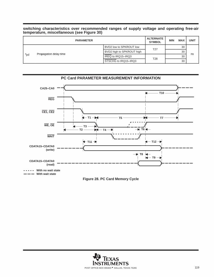
119POST OFFICE BOX 655303 • DALLAS, TEXAS 75265
switching characteristics over recommended ranges of supply voltage and operating free-airtemperature, miscellaneous (see Figure 30)
PARAMETERALTERNATE
SYMBOL MIN MAX UNIT
BVD2 low to SPKROUT lowT27
30
t d Propagation delay timeBVD2 high to SPKROUT high
T2730
nstpd Propagation delay timeIREQ to IRQ15–IRQ3
T2830
ns
STSCHG to IRQ15–IRQ3T28
30
PC Card PARAMETER MEASUREMENT INFORMATION
T8
T6
CA25–CA0
REG
CE1, CE2
WE, OE
WAIT
CDATA15–CDATA0(write)
T1 T7
CDATA15–CDATA0(read)
T2T3
T11
T10
T12
T4
With no wait stateWith wait state
T5
T9
Figure 28. PC Card Memory Cycle
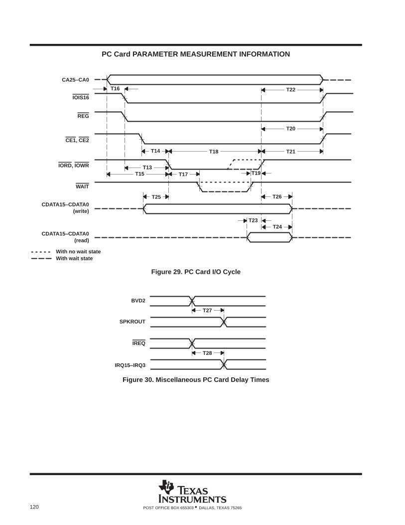
120 POST OFFICE BOX 655303 • DALLAS, TEXAS 75265
PC Card PARAMETER MEASUREMENT INFORMATION
T16
T23
T19
CA25–CA0
REG
CE1, CE2
IORD, IOWR
WAIT
CDATA15–CDATA0(write)
T14 T21
CDATA15–CDATA0(read)
T15T13
T25
T22
T26
T17
With no wait stateWith wait state
T18
T24
T20
IOIS16
Figure 29. PC Card I/O Cycle
BVD2
T27
SPKROUT
IREQ
T28
IRQ15–IRQ3
Figure 30. Miscellaneous PC Card Delay Times
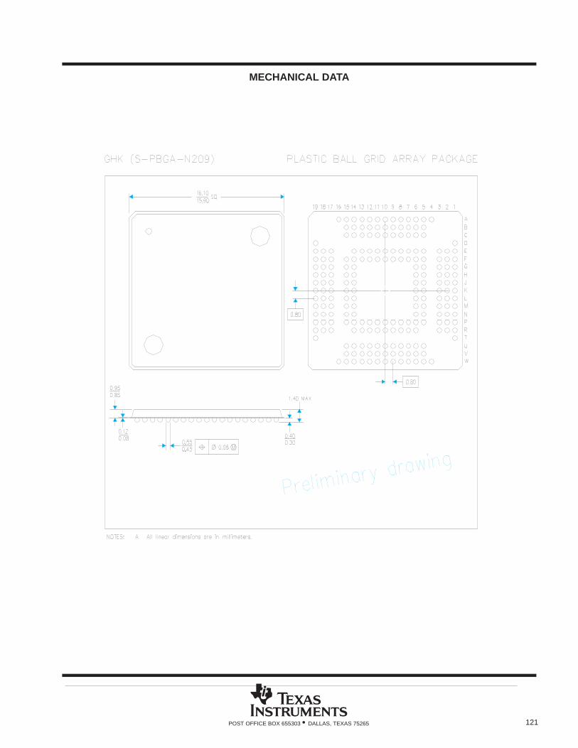
121POST OFFICE BOX 655303 • DALLAS, TEXAS 75265
MECHANICAL DATA
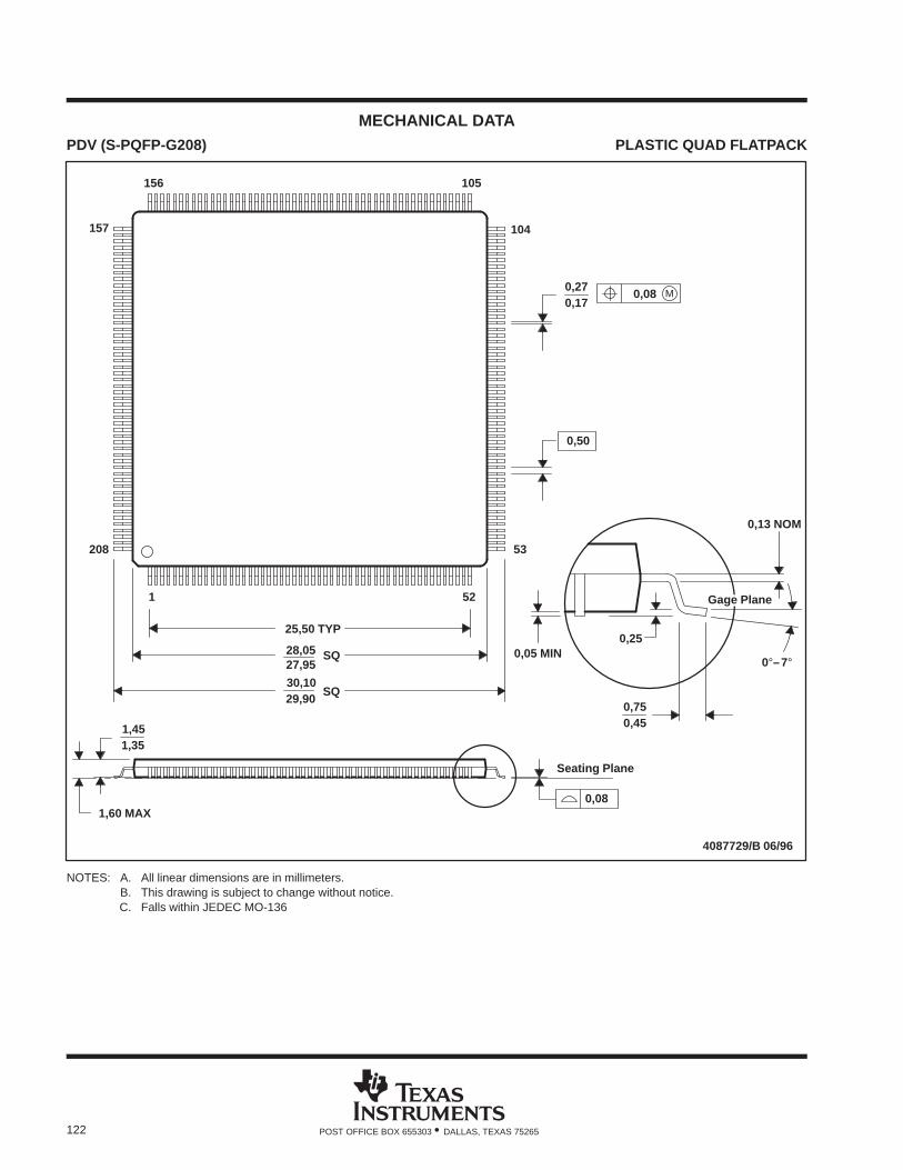
122 POST OFFICE BOX 655303 • DALLAS, TEXAS 75265
MECHANICAL DATAPDV (S-PQFP-G208) PLASTIC QUAD FLATPACK
0,13 NOM
105
104
53
0,270,17
0,25
0,450,75
0,05 MIN
52
Seating Plane
4087729/B 06/96
157
208
156
SQ
SQ
28,05
29,9030,10
27,95
25,50 TYP
1
1,60 MAX0,08
0,50
M0,08
0°–7°
Gage Plane
1,351,45
NOTES: A. All linear dimensions are in millimeters.B. This drawing is subject to change without notice.C. Falls within JEDEC MO-136
IMPORTANT NOTICE
Texas Instruments and its subsidiaries (TI) reserve the right to make changes to their products or to discontinueany product or service without notice, and advise customers to obtain the latest version of relevant informationto verify, before placing orders, that information being relied on is current and complete. All products are soldsubject to the terms and conditions of sale supplied at the time of order acknowledgement, including thosepertaining to warranty, patent infringement, and limitation of liability.
TI warrants performance of its semiconductor products to the specifications applicable at the time of sale inaccordance with TI’s standard warranty. Testing and other quality control techniques are utilized to the extentTI deems necessary to support this warranty. Specific testing of all parameters of each device is not necessarilyperformed, except those mandated by government requirements.
CERTAIN APPLICATIONS USING SEMICONDUCTOR PRODUCTS MAY INVOLVE POTENTIAL RISKS OFDEATH, PERSONAL INJURY, OR SEVERE PROPERTY OR ENVIRONMENTAL DAMAGE (“CRITICALAPPLICATIONS”). TI SEMICONDUCTOR PRODUCTS ARE NOT DESIGNED, AUTHORIZED, ORWARRANTED TO BE SUITABLE FOR USE IN LIFE-SUPPORT DEVICES OR SYSTEMS OR OTHERCRITICAL APPLICATIONS. INCLUSION OF TI PRODUCTS IN SUCH APPLICATIONS IS UNDERSTOOD TOBE FULLY AT THE CUSTOMER’S RISK.
In order to minimize risks associated with the customer’s applications, adequate design and operatingsafeguards must be provided by the customer to minimize inherent or procedural hazards.
TI assumes no liability for applications assistance or customer product design. TI does not warrant or representthat any license, either express or implied, is granted under any patent right, copyright, mask work right, or otherintellectual property right of TI covering or relating to any combination, machine, or process in which suchsemiconductor products or services might be or are used. TI’s publication of information regarding any thirdparty’s products or services does not constitute TI’s approval, warranty or endorsement thereof.
Copyright 1998, Texas Instruments Incorporated