Embed Size (px)
Citation preview

Circuits∗
October 16, 2003
Abstract
In this document, we build the TOY machine in hardware. Along the way we introduce Booleanfunctions, combinational circuits, and sequential circuits. Circuits are used to model the hardware ofdigital computers. They correspond directly with devices that we can build. In this document, weaddress the following questions:
• How can we build logical gates from wires and transistors?
• How can we build arithmetic circuits from logical gates?
• How can we build memory circuits?
• How can we combine all of these components to build a computer?
∗Copyright c© 2001, Kevin Wayne. Based on lecture notes by Robert Sedgewick.
1

CIRCUITS 2
Contents
1 Boolean Logic 31.1 Boolean Functions of Two Variables . . . . . . . . . . . . . . . . . . . . . . . . . . . . . . . . 31.2 Boolean Functions of 3 or More Variables . . . . . . . . . . . . . . . . . . . . . . . . . . . . . 4
2 Controlled Switches 4
3 Gates 5
4 Combinational Circuits 64.1 Multiway AND and OR gates . . . . . . . . . . . . . . . . . . . . . . . . . . . . . . . . . . . . 74.2 Sum-of-Products Method . . . . . . . . . . . . . . . . . . . . . . . . . . . . . . . . . . . . . . 84.3 Better circuit design . . . . . . . . . . . . . . . . . . . . . . . . . . . . . . . . . . . . . . . . . 94.4 Multiplexer . . . . . . . . . . . . . . . . . . . . . . . . . . . . . . . . . . . . . . . . . . . . . . 104.5 Decoder . . . . . . . . . . . . . . . . . . . . . . . . . . . . . . . . . . . . . . . . . . . . . . . . 114.6 Adder . . . . . . . . . . . . . . . . . . . . . . . . . . . . . . . . . . . . . . . . . . . . . . . . . 114.7 Subtracter . . . . . . . . . . . . . . . . . . . . . . . . . . . . . . . . . . . . . . . . . . . . . . . 13
5 Arithmetic Logic Unit 14
6 Sequential Circuits (memory) 146.1 Timing Diagrams . . . . . . . . . . . . . . . . . . . . . . . . . . . . . . . . . . . . . . . . . . . 156.2 Clock . . . . . . . . . . . . . . . . . . . . . . . . . . . . . . . . . . . . . . . . . . . . . . . . . 156.3 Flip-flops . . . . . . . . . . . . . . . . . . . . . . . . . . . . . . . . . . . . . . . . . . . . . . . 166.4 SR flip-flop . . . . . . . . . . . . . . . . . . . . . . . . . . . . . . . . . . . . . . . . . . . . . . 166.5 Clocked SR flip-flop . . . . . . . . . . . . . . . . . . . . . . . . . . . . . . . . . . . . . . . . . 186.6 Clocked D flip-flop . . . . . . . . . . . . . . . . . . . . . . . . . . . . . . . . . . . . . . . . . . 196.7 Register . . . . . . . . . . . . . . . . . . . . . . . . . . . . . . . . . . . . . . . . . . . . . . . . 206.8 Register file . . . . . . . . . . . . . . . . . . . . . . . . . . . . . . . . . . . . . . . . . . . . . . 216.9 1-bit counter . . . . . . . . . . . . . . . . . . . . . . . . . . . . . . . . . . . . . . . . . . . . . 226.10 Counter (optional) . . . . . . . . . . . . . . . . . . . . . . . . . . . . . . . . . . . . . . . . . . 23
7 Building a TOY Machine 24

CIRCUITS 3
1 Boolean Logic
Boolean logic is the foundation of digital computers. It is a rigorous mathematical system based on the twodistinct values true and false. Boolean logic is useful whenever there are two possible situations. A lightbulb is either on or off. In mathematics, a statement is either true or false. In digital circuits, a capacitoris either charged or uncharged. We universally associate 1 with on or true, and 0 with off or false, andrefer to the two binary digits as bits.
A mathematical function is an object that takes an input and produces an output. For a given functionf , the same input always produces the same output. Some familiar functions that transform one real inputinto one real output include: f(x) = x2 + 5, f(θ) = sin θ, f(x) = 9x/5 + 32. Functions can also take several
inputs, e.g., f(x, y) = x + y, f(x, y) =√
x2 + y2, f(r, θ) = r sin θ. Boolean functions are functions whoseinputs and output consists of only zeros and ones. For example, the NOT function takes one input bit andreturns the complementary bit.
NOT(x) =
{
1 if x = 0
0 if x = 1.
We will consider several fundamental Boolean functions, including AND, OR, and XOR. Then we’ll buildmore complicated functions from these primitive functions.
1.1 Boolean Functions of Two Variables
A Boolean function of two variables has two inputs, each of which can be 0 or 1. Thus, there are 4 possibleinput combinations. For each input combination, a Boolean function must specify either 0 or 1 as output.Thus, there are 24 = 16 distinct Boolean functions of two variables. The most important ones are AND andOR.
The AND function takes two input bits, and outputs 1 if both inputs are 1; otherwise 0.
AND(x, y) =
0 if x = 0 and y = 0
0 if x = 0 and y = 1
0 if x = 1 and y = 0
1 if x = 1 and y = 1.
For convenience, we often express a Boolean function more concisely using a truth table.
x y AND
0 0 00 1 01 0 01 1 1
Figure 1.1: The truth table for the AND function.
A truth table has a column for each of the inputs, and also for the Boolean function(s) that we areinterested in describing. There is a row for each possible combination of input values. A function of twovariables has 4 rows.
The OR function takes 2 input bits and outputs 1 if either input (or both) is 1; it outputs 0 if bothinputs are 0. The exclusive OR (XOR) function is similar to the OR function, except that it returns 1 ifexactly one of the inputs is 1 (but not both); otherwise it returns 0. Figure 1.2 gives a truth table for all 16Boolean functions of two variables, specifying the name of the function whenever possible.

CIRCUITS 4
x y ZERO AND x y XOR OR
0 0 0 0 0 0 0 0 0 00 1 0 0 0 0 1 1 1 11 0 0 0 1 1 0 0 1 11 1 0 1 0 1 0 1 0 1
x y NOR EQ y’ x’ NAND ONE
0 0 1 1 1 1 1 1 1 10 1 0 0 0 0 1 1 1 11 0 0 0 1 1 0 0 1 11 1 0 1 0 1 0 1 0 1
Figure 1.2: The truth table for all Boolean functions of two variables.
1.2 Boolean Functions of 3 or More Variables
Many applications involve functions of several variables. A Boolean function of three variables has threeinputs, each of which can be 0 or 1. Thus, there are 23 = 8 possible input combinations, and 8 rows in theits truth table. In general, a function of n variables has 2n possible input combinations. For each inputcombination, a Boolean function must specify either 0 or 1 as output. Thus, there are 22
3
= 256 distinctBoolean functions of three variables. In general, there are 22
n
different Boolean functions of n variables. Itis not unusual in engineering applications for a function to have thousands or millions of inputs. Even forn = 8, it is prohibitively expensive to fabricate physical processes for each of the 22
8
≥ 1077 such Booleanfunctions.
Generalizations of the AND and OR functions that take several inputs are important in designing circuits.An n-way AND function takes n inputs and outputs 1 if all n inputs are 1; otherwise it outputs 0. An n-wayOR function takes n inputs and outputs 1 if at least one of the n inputs is 1; otherwise it outputs 0.
The following two Boolean functions play an important role in designing arithmetic circuits. The n-waymajority function (MAJ) takes n input bits, and outputs 1 if at least half of the inputs are 1; otherwise itoutputs 0. The n-way odd parity function (ODD) takes n inputs, and output 1 if an odd number of inputsare 1; otherwise it outputs 0. Figure 1.3 summarizes the 3-way versions of the AND, OR, MAJ, and ODDfunctions.
x y z AND OR MAJ ODD
0 0 0 0 0 0 00 0 1 0 1 0 10 1 0 0 1 0 10 1 1 0 1 1 01 0 0 0 1 0 11 0 1 0 1 1 01 1 0 0 1 1 01 1 1 1 1 1 1
Figure 1.3: Some important Boolean functions of 3 variables.
2 Controlled Switches
Controlled switches are the fundamental building blocks of computer circuits, much like atoms are thefundamental building blocks of matter. A controlled switch has two inputs and one output, as illustrated inFigure 1. The main input is drawn on the top. The control input is drawn on the left; it controls whether ornot the main input is able to pass through the controlled switch. If the control input is set to pass (0), thenthe output is the same as the main input; if it is no pass (1), then the output is 0 regardless of the maininput.

CIRCUITS 5
control maininput input output
0 0 00 1 11 0 01 1 0
control input output
main input
Figure 1: A controlled switch and corresponding truth table.
A controlled switch is an abstraction of a physical process. Modern digital circuits are built from wiresand transistors, with current flowing through the circuit. However, circuits can also be built from otherprocesses. For example, in a “hydraulic circuit” water flows through pipes. In such a hydraulic circuit, thecontrol input of a switch is a valve; if it is closed then no water can pass through. Other types of controlledswitches include vacuum tubes, relays, and DNA. The discovery of a faster physical switch would profoundlychange the way computers are built; this is an active area of research. To gain a deeper understanding ofcomputer circuits, it is convenient to abstract away the physical details of the hardware involved. For therest of the document, we will assume that we have an idealized switch, and not worry about wiring, heatdissipation, electrical interference, circuit area, signal propagation delay, and other low level details.
3 Gates
A gate is a low-level circuit that is used as a primitive element in building more complicated circuits. Gatesare built by combining controlled switches with wires. We describe how to build NOT, OR, and AND gates.
The NOT gate can be implemented using a single controlled switch whose main input is always on, as inFigure 2. The OR gate can be implemented using three controlled switches, as in Figure 3. The AND gatecan be implemented using two controlled switches, as in Figure 4.1
x f0 11 0
x f = NOT(x)
1
x x’
Figure 2: Implementing a NOT gate using one switch, its truth table, and its schematic symbol.
The AND, OR, and NOT gates are used so frequently that they have special schematic symbols. Insteadof drawing the underlying controlled switches, it is standard to draw an AND gate as a half circle. Weimplicitly understand that the half circle represents 2 controlled switches, configured as in Figure 4. Similarly,we represent an OR gate with a crescent. A NOT gate is drawn as a triangle with a circle at its tip.
1Building an AND gates from pass transistors would require four transistors, since all exposed main inputs must be on.

CIRCUITS 6
x y u v f0 0 1 1 00 1 1 0 11 0 0 0 11 1 0 0 1
x
y f = OR(x, y)
1
1
u
v
xy x + y
Figure 3: Implementing an OR gate using three switches, its truth table, and schematic symbol. If x andy are both set to pass (0), then the control input of the third switch (v) is 1; otherwise it is 0. The thirdswitch acts like a NOT gate, and its output is v′. This is exactly the OR function.
x y u f0 0 1 00 1 0 01 0 1 01 1 0 1
y f = AND(x, y)
x1
u
xy xy
Figure 4: Implementing an AND gate using two switches, its truth table, and schematic symbol. The leftswitch acts like a NOT gate; it’s output is y′. The second transistor has main input x and control input y′.It’s output is 1 if and only if both x and y are both 1.
4 Combinational Circuits
Combinational circuits are physical hardware used to model Boolean functions. They are comprised of gatesand wires in a directed acyclic configuration. Each wire (other than the input wires) connects the output ofone gate to the input of another gate. There is no chain of wires and gates that form a directed cycle orloop. (See Figure 5.) This would cause the output of one gate to ultimately affect one of its inputs. Sucha directed cycle is called a feedback loop. Circuits with feedback loops are called sequential circuits, and areconsidered in Section 6.
In a combinational circuit, each gate takes a prespecified number of input wires, evaluates the inputaccording to the Boolean function associate with the gate, and transmits the value to the output wire.Here’s a procedure for determining the output of a combinational circuit. Start with the input wires, whosevalues are known. Propagate these values along the wire to the gates to which they connect. Once all of theinputs to a gate are known, propagate the information along its output wire. Continue this process until thestatus of all wires and gates is known. Since combinational circuits have no feedback loops, this process iswell-defined, and guarantees a unique value for each gate and wire upon termination.
In principle, it is possible to build a combinational circuit for any Boolean function directly from controlledswitches. However, the resulting design could be overwhelmingly complex, due to the huge number of

CIRCUITS 7
xy
zy
x
Figure 5: The left circuit is a combinational circuit since it has no feedback loops. The right circuit is asequential circuit since it has a feedback loop.
switches. Instead, it is convenient to build circuits from somewhat higher level building blocks, namelythe NOT, AND, and OR gates. This modular approach will facilitate the construction, as well as ourunderstanding, of higher level circuits. By working at this higher level of abstraction, we can concentrate ondesigning more complicated circuits, without worrying about the lower level details. Of course, each of theNOT, AND, and OR gates that we use in the process will ultimately be physically realized with transistors(or other controlled switches). Again, depending on the type of circuit we are designing, we may wish towork at a still higher level of abstraction, and use higher level circuits as primitive circuit elements.
4.1 Multiway AND and OR gates
We describe how to build an n-way AND gate. Recall, an n-way AND gate outputs 1 if all of its inputs are 1;otherwise it outputs 0. First, we build a 3-way AND gate. We could start from switches, but instead, we buildit by combining two 2-way AND gates. They key observation is that AND(x, y, z) = AND(x,AND(y, z)).Similarly, we can build an n-way AND gate using (n − 1) 2-way AND gates. A 3-way and an 8-way ANDgate are shown in Figure 6.
An n-way OR gate outputs 1 if at least 1 of its inputs is 1; otherwise it outputs 0. Designing an n-wayOR gate is very similar to an n-way AND gate because OR(x, y, z) = OR(x,OR(y, z)).
AND(x, y, z)
xy
z
AND(x0, . . . , x7)
x0x1
x2x3
x4x5
x6x7
Figure 6: A 3-way AND gate built from two 2-way AND gates, an 8-way AND gate built from seven 2-wayAND gates, and their schematic symbols.

CIRCUITS 8
4.2 Sum-of-Products Method
The sum-of-products method is a systematic process for designing any Boolean function using only AND,OR, and NOT gates. First we introduce some standard notation that will serve to explain the name “sum-of-products.” We use the “product” xy to denote AND(x,y), the “sum” x + y to denote OR(x,y), and x′ todenote NOT(x). The product notation agrees with your intuition from multiplying integers, since the valuesare always 0 or 1. With the summation notation, 0 + 0 = 0, 1 + 0 = 0 + 1 = 1, as usual, but note that1 + 1 = 1. The interested reader can verify that many familiar arithmetic laws hold with this new definitionof product and sum.2 By convention, the NOT operation has the highest precedence, followed by AND, andthen OR. So, for example, xy′ + z is correctly interpreted as (x(y′)) + z.
We illustrate the sum-of-products method by designing an XOR gate using only AND, OR, and NOTgates. Recall the XOR(x,y) function is 1 if and only if exactly one of x or y is 1. We first consider twosomewhat simpler functions. The function x′y is 1 if and only if x = 0 and y = 1. The function xy′ is 1 ifand only if x = 1 and y = 0. Note that XOR(x,y) is 1 if and only if x′y = 1 or xy′ = 1. Thus, the Booleanfunction x′y + xy′ is identical to the desired XOR(x,y) function.
x y XOR x′y xy′ x′y + xy′
0 0 0 0 0 00 1 1 1 0 11 0 1 0 1 11 1 0 0 0 0
Figure 7: An XOR circuit.
The general sum-of-products procedure involves forming an AND term for each 1 in the original function’struth table column. The goal is to have each AND term be 1 if and only if the corresponding input row is 1.Finally all of these AND terms are OR’ed together, so that if any one of them is 1, then the OR expressionis 1.
The sum-of-products method naturally extends to handle functions with more than 2 inputs. Recallthe MAJ(x, y, z) function returns 1 if and only if 2 or more of its inputs are 1. Using the sum-of-productsmethod, we form an AND term for each of the 4 input combinations for which MAJ(x, y, z) outputs 1:(x, y, z) = (0, 1, 1), (1, 0, 1), (1, 1, 0), (1, 1, 1). The four AND terms are x′yz, xy′z, xyz′, and xyz, respectively.Thus MAJ(x, y, z) = x′yz + xy′z + xyz′ + xyz.
x y z MAJ x′yz xy
′z xyz
′xyz x
′yz + xy
′z + xyz
′ + xyz
0 0 0 0 0 0 0 0 00 0 1 0 0 0 0 0 00 1 0 0 0 0 0 0 00 1 1 1 1 0 0 0 11 0 0 0 0 0 0 0 01 0 1 1 0 1 0 0 11 1 0 1 0 0 1 0 11 1 1 1 0 0 0 1 1
2For example, the usual commutative, distributative, and associative rules of algebra hold: x + y = y + x, x · y = y · x,(x + y) + z = x + (y + z), (x · y) · z = x · (y · z), x · (y + z) = x · y + x · z, (x′)′ = x. DeMorgan’s identities (ab)′ = a′ + b′ and(a + b)′ = a′ b′ are also useful.

CIRCUITS 9
4.3 Better circuit design
It is possible to design different circuits that produce the same output, given the same input. The sum-of-products method provides a recipe for building combinational circuits. It is guaranteed to work, but maynot always produce the “best” circuit. For example, a simpler majority circuit design is MAJ(x, y, z) =xy + xz + yz. See Figure 8.
There are two common quantitative criteria for measuring the quality of a circuit. The size of a circuit isthe number of gates that it contains. This measure reflects the resources needed to build the hardware. Thedepth of a circuit is the length of the longest path from a circuit input to a circuit output. Physical circuitscan propagate their values in parallel. The depth reflects the time needed to evaluate the circuit. Circuitswith smaller depth run faster. The two circuits in Figure 8 both compute the majority function of threeinputs. The first circuit has size 8 and depth 4, while the second has size 4 and depth 3. Designing circuitsof small size and depth is an important and challenging problem, but we will not concentrate on these issueshere.
Figure 8: A 3-way majority circuit built using the sum-of-products method (left) and a simpler circuit(right).

CIRCUITS 10
4.4 Multiplexer
A multiplexer (or mux for short) is a useful circuit for selecting from one of several possibilities. An n-bitmultiplexer has n select inputs, 2n data inputs, and a single output. The n select inputs are interpreted asa binary number. The input wire (which are numbered from 0 to 2n − 1 from top to bottom) correspondingto this binary number is selected, and its value becomes the output of the multiplexer circuit. We will usemultiplexers in section 6.8 to build TOY registers and main memory.
Figure 9: The interface and implementation of a 3-bit multiplexer.
Sometimes it is convenient to have a multiplexer select from a bank of n input buses, each of whichcontains k wires. Think of n = 256 as being the number of memory locations and k = 16 as being thenumber of bits stored in a register. This circuit is useful to extract the contents of one memory location.We call such a circuit a k-wide n-to-1 multiplexer. We can implement it by layering k n-to-1 multiplexers.Figure 10 shows a multiplexer that selects from one of two possible 4-bit buses.
Figure 10: The interface and implementation of a 4-wide 2-to-1 multiplexer.

CIRCUITS 11
4.5 Decoder
A decoder is a circuit that converts from binary to unary. An n-bit decoder has n select inputs and 2n
outputs. See Figure 11 for a 3-bit decoder. Exactly one of the 2n outputs is 1; the rest are 0. The selectinputs determine which output is on. Interpret the n inputs as a binary number (read left to right). Theoutput wire corresponding to this binary number is turned on; all other output wires are off. E.g., if thethree inputs are 1, 1, and 0, then output wire number 6 is on. The outputs wires are numbered 0 to 2n - 1from top to bottom. In Section 6.8 we will use this circuit to build TOY registers and main memory.
Figure 11: The interface and implementation of a 3-bit decoder.
4.6 Adder
We describe how to design a circuit to perform integer addition. This illustrates that simple Boolean circuitscan be used to perform arithmetic.
Since computers store only zeros and ones, we build a circuit that adds in binary (base 2). Adding twonumbers in binary is much like adding two numbers in decimal (base 10). In decimal, we first add the two1’s digits together; if the sum is 10 or more, we carry a 1 over to the 10’s digit. Then we add the two 10’sdigits and the carry bit; if the resulting sum is 10 or more, we carry a 1 over to the 102 = 100’s digit. Thisprocess is repeated until we are finished. In binary, everything is the same except that 10 is replaced with 2.
We need to formalize this procedure in order to build an adder circuit. Suppose we want to computes = x + y, where x and y are nonnegative 8-bit binary integers. Note that in this section the symbol ‘+’denotes ordinary addition, not the Boolean OR function. We notate the ith digit of x, y and s by xi, yi, andsi, respectively. E.g., if x = 01100101 then x = x7x6x5x4x3x2x1x0 and x0 = 1, x1 = 0, x2 = 1, and so on.We wish to compute:
x7 x6 x5 x4 x3 x2 x1 x0
+ y7 y6 y5 y4 y3 y2 y1 y0
s7 s6 s5 s4 s3 s2 s1 s0

CIRCUITS 12
First observe
s0 =
0 if x0 + y0 = 0
1 if x0 + y0 = 1
0 if x0 + y0 = 2.
Equivalently, s0 = ODD(x0, y0, 0), where ODD is the 3-way odd parity function discussed in Section 1.2.Now we give a Boolean expression for the carry bit. We will use ci to denote the carry bit produced whenadding the ith digits. It follows that
c0 =
0 if x0 + y0 = 0
0 if x0 + y0 = 1
1 if x0 + y0 = 2.
Equivalently, c0 = MAJ(x0, y0, 0), where MAJ is the 3-way majority function described in Section 1.2. Thismethod extends to computing the ith digit in the sum, and the ith carry bit. In general
si =
{
0 if xi + yi + ci−1 = 0 or 2
1 if xi + yi + ci−1 = 1 or 3.and ci =
{
0 if xi + yi + ci−1 = 0 or 1
1 if xi + yi + ci−1 = 2 or 3.
Equivalently, si = ODD(xi, yi, ci−1) and ci = MAJ(xi, yi, ci−1). Note that ci−1 must be computed beforezi or ci. We see that the MAJ and ODD circuits play an important role in binary addition.
To build an n-bit ripple-carry adder, it is convenient to first define a 1-bit adder that takes 3 inputs, sayx, y, and z, and produces 2 outputs, say S (sum) and C (carry bit). We design the circuit so that S =ODD(x, y, z) and C =MAJ(x, y, z). This circuit is described in Figure 12. Now, by chaining together 4 ofthese 1-bit adders, we can build an 4-bit ripple-carry adder, as in Figure 13. In general, an n-bit adderhas 2n inputs, n corresponding to the first summand x, and n corresponding to the second summand y. Itproduces n outputs, corresponding to the sum s = x + y. To avoid overflow, we could design an n-bit adderthat adds two n-bits integers and return an (n + 1)-bit integer. Instead, we truncate the result to n-bits,e.g., 1111 + 0011 = 0010.
MAJ
ODD
x
y
z
C
S
1-bitadder
x y z
S
C
Figure 12: A 1-bit adder and its schematic symbol.

CIRCUITS 13
1-bitadder
x y z
0x0 y0
S
C
s0
1-bitadder
x y z
x1 y1
S
C
s1
1-bitadder
x y z
x2 y2
S
C
s2
1-bitadder
x y z
x3 y3
S
C
s3
x3 x2 x1 x0 y3 y2 y1 y0
4-bit adder
z3 z2 z1 z0
Figure 13: A 4-bit adder and its schematic symbol.
4.7 Subtracter
In the previous section we saw how to build a circuit to perform binary addition. In principle, we coulduse the exact same approach and build a binary subtracter circuit. In practice, it is simpler to directlyreconfigure the adder circuit to perform subtraction.
To subtract y from x, we will perform the addition x + (−y). Recall that with 2’s complement integers,to convert from y to −y involves flipping all of the bits, and then adding one. This is particularly easy toimplement in hardware. To flip the bits, we use a NOT gate. Adding 1 to a number seems like a biggerchallenge. This is where we use the carry-in input to the least significant bit. For addition, we always setthe carry-in of the least significant bit to be 0, but by changing it to 1, we effectively add 1 to the entireresult. Figure 14 gives the details.
Figure 14: The interface and implementation of a 4-bit subtracter.

CIRCUITS 14
5 Arithmetic Logic Unit
The arithmetic logic unit (ALU) is the workhorse circuit of a computer. It is responsible for performing theTOY arithmetic operations (addition and subtraction) and the TOY logic operations (bitwise AND, bitwiseXOR, shift left, shift right).
The ALU consists of several control inputs and separate circuit components for addition, bitwise AND,bitwise XOR, and shifting. It performs all 4 computations in parallel, and then selects the appropriateoutput depending on the control inputs.
Figure 15: The implementation of the TOY ALU.
6 Sequential Circuits (memory)
Combinational circuits are only capable of performing a computation once, because the values of the gatesand wires do not change over time. Thus, if we want to perform ten million additions, we would have tobuild ten million individual combinational adder circuits. By allowing feedback, the values in a sequentialcircuit may change over time. This is the essential component needed to make circuits that can “write”and “read” information to and from “memory.” This enables sequential circuits to reuse circuit elements,thereby greatly reducing the hardware requirements for building a computer.
Timing. Until now, we have assumed that gates process their input and produce output instantaneously.In fact, it takes a small amount of time for current to transmit through a wire. This wire timing delaydepends on the length and material properties of the wire. It also takes time for gates to transform theirinput into output. This gate timing delay depends on the configuration, wiring, and number of controlledswitches in the gate design. As you would expect, a 3-switch OR gate has a higher gate timing delay thana 1-switch NOT gate.

CIRCUITS 15
Understanding the output of a sequential circuit is more difficult than with combinational circuits. Withcombinational circuits, the input values uniquely determine a value for every gate and wire in the circuit.With sequential circuits, the gate and wire values may change over time. Here’s a somewhat simplified viewof how a sequential circuit operates. At time t, some of the wires are on, and some are off. The state of thecircuit at time t + dt is determined by computing the output of every gate in parallel, using the circuit stateat time t. This process is repeated. The state of the circuit at time t + 2dt is determined by computing theoutput of every gate, but now using the circuit state at time t + dt. This process is repeated for each timequantum. For simplicity, we have assumed that the gate timing delay of every gate is exactly dt, and thatthe wire timing delay is negligible. In reality, each gate has its own timing delay, and wire transmission timeis relatively small, but not zero. Subtle differences in timing delays can create bizarre behavior in poorlydesigned circuits. Consider the circuit in Figure 16. What is the value of the output wire over time? Itdepends on the timing delays of the gates. The output of the NOT gate constantly changes its value from1 to 0. As a result, it is not possible to accurately determine the output of the circuit. This is known asa race condition and is the bane of circuit design. We will only build circuits that do not directly rely onthe timing delays; we only make the reasonable assumption that the timing delays are small, relative to theclock rate.
0
1
Figure 16: A race condition: the output of the NOT gate oscillates between 0 and 1, so the output of theOR gate depends on the gate timing delays.
6.1 Timing Diagrams
Timing diagrams are important for understanding the output of sequential circuits. For combinationalcircuits, a truth table characterizes the behavior of the circuit for all possible input combinations. Forsequential circuits, it is not possible to enumerate all possible input combinations, since the input is really astream of inputs that change over time. We use a timing diagram to chart the state of the circuit over timefor one particular input stream. We plot time on the x-axis and the on/off status of the wire on the y-axis.
6.2 Clock
To build computers, we need to be able to synchronize and coordinate various computations. Computers usean external clock to accomplish this. The clock is an abstraction that transmits on and off pulses at regularintervals. The pulse lasts for a relatively small amount of time. See Figure 17 for a timing diagram of atypical clock. The clock in a 500MHz Pentium pulses 500 million times a second. The clock speed determinesthe rate at which instructions are processed, and greatly influences the overall speed of the computer.

CIRCUITS 16
time
clockoff
on
Figure 17: The timing diagram of a clock.
Circuits are designed so that new computations can only be initiated when the clock is on. The compu-tations can proceed while the clock is off, but it is often desirable for it to finish before the next clock pulse.Building circuit elements that will begin and finish execution within a single clock tick depends directly onthe speed at which the underlying switches operate. The invention of a faster switch would enables com-puters to use a faster clock. Different computer architectures use different instruction sets. RISC (reducedinstruction set computers) machines can have faster clocks, but this comes at the expense of perfoming amore limited range of instructions per clock cycle.
6.3 Flip-flops
A flip-flop is a simple sequential circuit that is capable of “storing a bit.” To accomplish this, the flip-flopcreates a feedback loop which transmits current (or no current) across the loop. When the feedback loophas current, we interpret it as storing the bit 1; when there is no voltage we interpret it as storing the bit 0.Flip-flops are used to build registers and memory. We consider several types of flip-flops below.
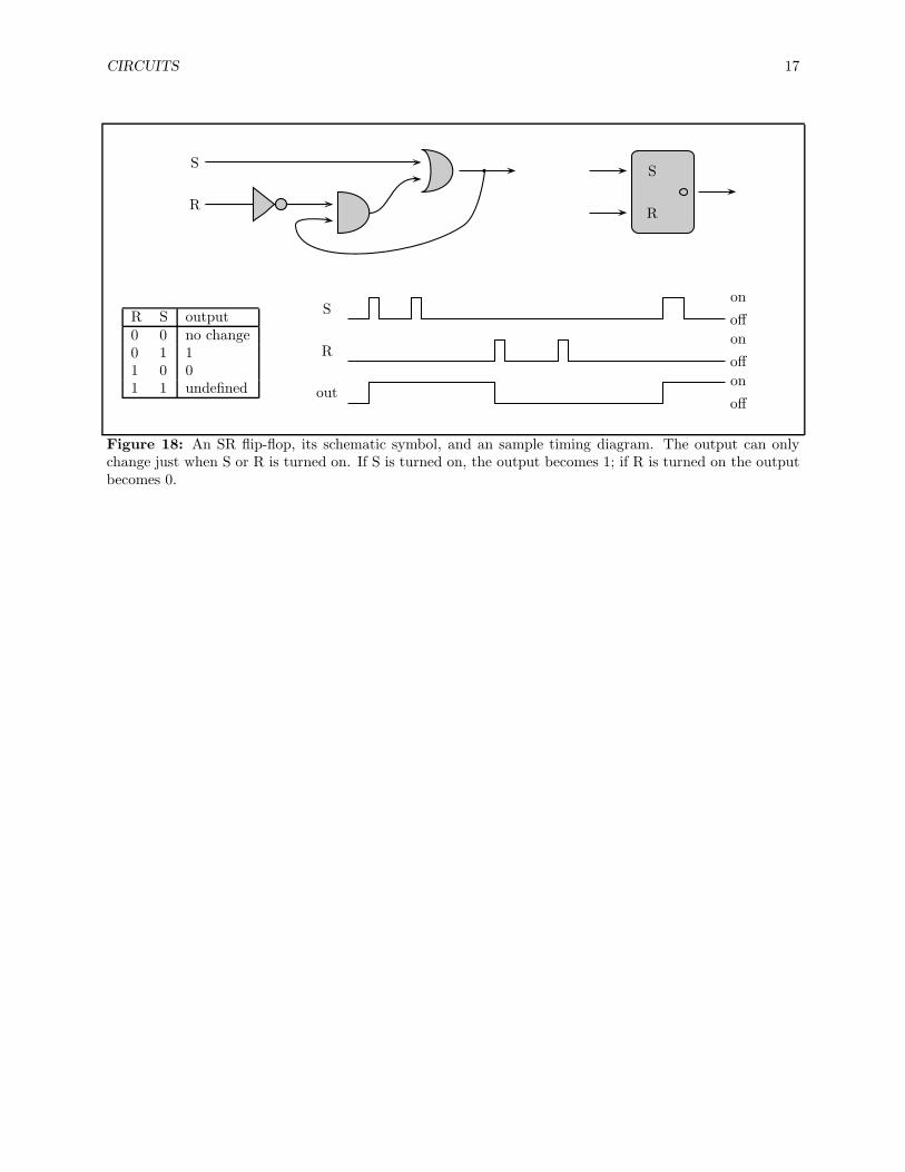
6.4 SR flip-flop
The SR flip-flop is the simplest type of flip-flop; the corresponding circuit and schematic symbol are shownin Figure 18. It has two inputs, labeled S (set) and R (reset). It has one output which represents the value ofthe stored bit. It works as follows. If S and R are both 0 (neither line is selected), then the value propagatedaround the feedback loop is unchanged. If the bit was 1, then it remains 1; if it was 0, then it remains 0.If S is selected (set to 1), then the value 1 will be transmitted around the feedback loop. If R is selected(set to 1), then the value 0 will be transmitted around the feedback loop. The output is undefined if both Sand R are selected at the same time – we will see a slightly more complicated flip-flop that overcomes thispotential pitfall.
CIRCUITS 17
R
SS
R
out
R
S
off
on
off
on
off
on
R S output0 0 no change0 1 11 0 01 1 undefined
Figure 18: An SR flip-flop, its schematic symbol, and an sample timing diagram. The output can onlychange just when S or R is turned on. If S is turned on, the output becomes 1; if R is turned on the outputbecomes 0.

CIRCUITS 18
6.5 Clocked SR flip-flop
A clocked SR flip-flop is the same as an SR flip-flop except that all actions are synchronized with the clock.It has three inputs: S (set), and R (reset), and Cl (clock). If the clock is on and S is selected, then theflip-flop will store a 1. If the clock is on and R is selected, then the flip-flop will store a 0. If the clockis off, then the value currently stored in the flip-flop will remain unchanged. A clocked SR flip-flop can beimplemented by ANDing the S and R inputs with the clock as in Figure 19.
S
R
S
Cl
R
S
R
Cl
out
R
S
Cl
off
on
off
on
off
on
off
on
Figure 19: A clocked SR flip-flop, its schematic symbol, and a sample timing diagram. The output canonly change when the clock is on.

CIRCUITS 19
6.6 Clocked D flip-flop
A clocked D flip-flop is useful for directly copying an input bit value into memory. A clocked D flip-flop hastwo inputs: D (data) and Cl (clock). If the clock is on, then the bit value on D is copied and stored in theflip-flop: if D is 0, then a 0 is stored, if D is 1, then a 1 is stored. If the clock is off, then the value currentlystored in the flip-flop remains unchanged. A D flip-flop can be implemented from a clocked SR flip-flop andone NOT gate, as illustrated in Figure 20. The D input is wired directly to the S input of a clocked SRflip-flop, and indirectly through a NOT gate to the R input the SR flip-flop. The clock of the D input iswired directly to the clock input of the SR flip-flop. When D is on, S is on and R is off. When D is off, Sis off and R is on. Thus, exactly one of the inputs to the clocked SR flip-flop is always on. If the clock ison, then this effectively copies the bit value of the D wire into the flip-flop “memory.” If the clock is off, thememory remains unchanged.
S
R
ClClD
D
Cl
out
D
Cl
off
on
off
on
off
on
Figure 20: A D flip-flop, its schematic symbol, and a sample timing diagram. The output only changeswhen the clock is on: the output is the same as D during this period.

CIRCUITS 20
6.7 Register
A n-bit register is a repository for storing n bits. It has n input values x0, . . . , xn−1, and n output valuesy−, . . . , yn−1. It also has a write input that must be set in order for any data to be written to the register.The values y0, . . . , yn−1 are stored in the n flip-flops and are always available on the output wires. Thesevalues do not change unless the write input is on. If the write input is on, then the values x0, . . . , xn−1 arewritten into the n flip-flops. Think of x as being the output of some calculation that we wish to store awayin y for later reuse. We implement a register in Figure 21 as a sequence of clocked D flip-flops.
An 8-bit register corresponds directly with the TOY program counter. In the next section we will seehow to combine 256 16-bit registers to implement the TOY main memory.
Figure 21: The interface and implementation of a 16-bit register.

CIRCUITS 21
6.8 Register file
Modern computers contain millions or billions of bits of memory. A register file provides a systematic methodto organize and manipulate them. A k × n register file is a bank of n registers, each of which stores k bits.It contains k data inputs, k data outputs, log2 n address inputs, a clock input, and a write input. At anypoint in time, exactly one of the n registers can be accessed: the log2 n address inputs specify which one.The contents of this addressed register appear on the k output wires. If the clock and write inputs are on,then the contents of the k input wires will be immediately copied to the addressed register.
We implement a k × n register file as a sequence of n k-bit registers along with some combinationalcircuitry to access the registers. A k-wide n-to-1 multiplexer is ideally suited for selecting which register toselect as the output. For writing, we used a log2 n-bit decoder, and wire its n outputs through an AND gateto the write input of the corresponding register. Since the contents of a register can only change if the writeinput is on, this ensures that only the appropriate register is overwritten. Figure 22 gives the details for a256 × 16 register file.
Figure 22: The interface and implementation of a 256 ×16 register file.

CIRCUITS 22
6.9 1-bit counter
A 1-bit counter or toggle is a circuit that takes one clock input and has one output such that the outputchanges (from 0 to 1, or from 1 to 0) each time the input goes from on to off. We will use this circuit tochoreograph the fetch-execute cycle of the TOY machine. When the counter’s output is 0, the machine willbe fetching the next instruction; when it’s output is 1, the machine will be executing the current instruction.
We build a 1-bit counter by wiring together two D flip-flops through a NOT gate. Figure 23 describesthe interface, implementation, and timing diagram of a toggle.
The toggle’s output only changes when its clock input goes from on to off. This property enables refinedcontrol over when actions will occur. For example, after an instruction like R[1] <- R[1] + R[2], we wantto be sure that we don’t overwrite the contents of register 1 until the end of the execute cycle; otherwisethis updated value could get used in the addition instead of the original value. To ensure that this feedbackdoesn’t occur, we will only allow overwriting a register to occur when the clock and the toggle are both 1,i.e., at the very end of the execute phase.
D
ClmasterslaveCl
Cl 1-bitcounterCl
out
Cl
off
on
off
on
Figure 23: A 1-bit counter, its schematic symbol, and a sample timing diagram. The output changes whenthe input goes from on to off.

CIRCUITS 23
6.10 Counter (optional)
A n-bit counter has one input and n outputs. The counter counts the number of times that the input goesfrom on to off. The n outputs store this quantity as a binary number. Although the counter is a usefulcircuit in many contexts, we do not use it in the design of the TOY machine.
We implement an n-bit counter by chaining together n 1-bit counters in series, as in Figure 24.3 Theoutput c0 is exactly the output of a single 1-bit counter. It goes from 0 to 1 just after the 1st, 3rd, 5th, and7th clock pulses, i.e., every other clock pulse. Output c0 is the input to the next 1-bit counter. Thus, theoutput c1 changes when c0 goes from 1 to 0. Hence, c1 changes from 0 to 1 just after the 3rd, 7th, 11th,15th clock pulses, i.e., every 4th clock pulse. Similarly, output c2 changes from 0 to 1 every 8th clock pulse,and in general, ci changes from 0 to 1 every 2i+1 clock pulses.
Cl 1-bitcounterCl
c0
Cl 1-bitcounter
c1
Cl 1-bitcounter
c2
3-bitcounter
c0
c1
c2
Cl
c0
c1
c2
off
on
off
on
off
on
off
on
000 001 010 011 100 101 110 111 000 001
Figure 24: A 3-bit counter, its schematic symbol, and a sample timing diagram.
3Although this is the simplest way to build a counter, it is not recommended in practice. Because of timing delays, the n
outputs of the circuit are not determined simultaneously; bit 0 is known first, then bit 1, then bit 2, and so on.

CIRCUITS 24
7 Building a TOY Machine
We have described all of the components need to build the TOY computer: ALU, clock, counter, registers,and register files. We will now describe how to assemble these pieces and produce a blueprint for the TOYmachine. There are 3 remaining steps.
1. Determine datapath requirements. We need to ensure that all of the data can be routed to theappropriate place.
2. Establish clocking methodology. The TOY machine has two phases: fetch and increment. Both phasesmay to access the same hardware resources. For example, the fetch phase needs to read from mainmemory to grab the next instruction to be executed. Executing an TOY load instruction also requiresaccess to main memory. We need to choreograph the fetch-execute cycle so that they do not interferewith each other.
3. Analyze how to implement each instruction, and determine settings of control signals.
Unfortunately, we do not have any notes on this material. Please consult the lecture notes.