Embed Size (px)
Citation preview
1
AMPLIFICATION CIRCUITS AND PATTERNING METHODS OF ORGANIC FIELD-EFFECT TRANSISTORS
NSF Summer Undergraduate Fellowship in Sensor Technologies
Hank Bink (Electrical and Computer Engineering) – Lafayette College
Advisor: Cherie Kagan
Abstract
Organic transistor technology holds great promise for creating a conformal, human-safe electronic neural interface. These interfaces must amplify the low, microvolt-range brain signals so they can be utilized in analog and digital applications. Brain signals from sensors must be relayed to the transistor’s gate through the dielectric and semiconductor layers, as well as through an encapsulant which keeps the device shielded in the aqueous brain environment. In order to test their amplification gains, silicon wafer-based ambipolar organic transistors with a pentacene semiconductor were tested under nitrogen in amplifying configurations including common source and cascode. Gains for common source amplifiers with resistors were up to 3.5V/V. Gains for the cascode setup revealed the same results as common source. Both the common source and cascode topologies exhibited very low bandwidth with -3dB points of 35 and 25 hertz, respectively. Parylene C, a biologically safe polymer, is a leading candidate to encapsulate pentacene transistors and serve as a dielectric layer between the devices and sensing electrodes. We tested etching of this parylene as well as the dielectric materials benzocyclobutene (BCB) and spin-on-glass (SoG) using both oxygen and SF6 plasma etching. Parylene was etched at a rate of 0.2μm/min with O2 plasma. BCB and SoG did not exhibit useful etching under O2 or SF6 plasma.
2
Table of Contents
Title and Author Information...........................................................................................................1
Abstract............................................................................................................................................1
Table of Contents.............................................................................................................................2
1. Introduction..................................................................................................................................3
2. Background..................................................................................................................................3
2.1 Fundamentals of Field-Effect Transistors......................................................................4
2.2 Organic Field-Effect Transistors: Makeup and Characteristics.....................................4
2.2.1 Pentacene: Use as a Semiconductor................................................................5
2.2.2 Unipolar and Ambipolar Transistors..............................................................5
2.2.3 Advantages and Disadvantages over MOSFETs............................................5
2.3 Organic Transistor Amplifying and Digital Circuits.....................................................6
2.4 Parylene: Use as an Encapsulant....................................................................................6
2.5 Dry Etching to Create Via Holes...................................................................................6
3. Experimental Methods.................................................................................................................7
3.1 Amplifying Circuits.......................................................................................................7
3.2 Etching Setup.................................................................................................................8
4. Results and Analysis....................................................................................................................9
4.1 Amplification.................................................................................................................9
4.2 Patterning Methods......................................................................................................13
5. Conclusions................................................................................................................................14
6. Recommendations......................................................................................................................14
7. Acknowledgements....................................................................................................................14
3
8. References..................................................................................................................................14
1. Introduction
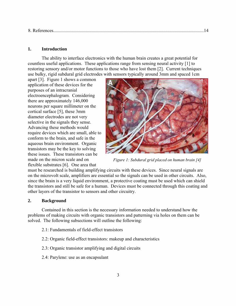
The ability to interface electronics with the human brain creates a great potential for countless useful applications. These applications range from sensing neural activity [1] to restoring sensory and/or motor functions to those who have lost them [2]. Current techniques use bulky, rigid subdural grid electrodes with sensors typically around 3mm and spaced 1cm apart [3]. Figure 1 shows a common application of these devices for the purposes of an intracranial electroencephalogram. Considering there are approximately 146,000 neurons per square millimeter on the cortical surface [5], these 3mm diameter electrodes are not very selective in the signals they sense. Advancing these methods would require devices which are small, able to conform to the brain, and safe in the aqueous brain environment. Organic transistors may be the key to solving these issues. These transistors can be made on the micron scale and on flexible substrates [6]. One area that must be researched is building amplifying circuits with these devices. Since neural signals are on the microvolt scale, amplifiers are essential so the signals can be used in other circuits. Also, since the brain is a very liquid environment, a protective coating must be used which can shield the transistors and still be safe for a human. Devices must be connected through this coating and other layers of the transistor to sensors and other circuitry.
2. Background
Contained in this section is the necessary information needed to understand how the problems of making circuits with organic transistors and patterning via holes on them can be solved. The following subsections will outline the following:
2.1: Fundamentals of field-effect transistors
2.2: Organic field-effect transistors: makeup and characteristics
2.3: Organic transistor amplifying and digital circuits
2.4: Parylene: use as an encapsulant
Figure 1: Subdural grid placed on human brain [4]
4
2.5: Dry etching to create via holes
2.1 Fundamentals of Field-Effect Transistors
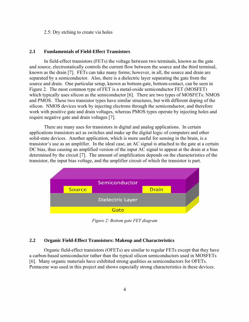
In field-effect transistors (FETs) the voltage between two terminals, known as the gate and source, electrostatically controls the current flow between the source and the third terminal, known as the drain [7]. FETs can take many forms; however, in all, the source and drain are separated by a semiconductor. Also, there is a dielectric layer separating the gate from the source and drain. One particular setup, known as bottom-gate, bottom-contact, can be seen in Figure 2. The most common type of FET is a metal-oxide semiconductor FET (MOSFET) which typically uses silicon as the semiconductor [6]. There are two types of MOSFETs: NMOS and PMOS. These two transistor types have similar structures, but with different doping of the silicon. NMOS devices work by injecting electrons through the semiconductor, and therefore work with positive gate and drain voltages, whereas PMOS types operate by injecting holes and require negative gate and drain voltages [7].
There are many uses for transistors in digital and analog applications. In certain applications transistors act as switches and make up the digital logic of computers and other solid-state devices. Another application, which is more useful for sensing in the brain, is a transistor’s use as an amplifier. In the ideal case, an AC signal is attached to the gate at a certain DC bias, thus causing an amplified version of the input AC signal to appear at the drain at a bias determined by the circuit [7]. The amount of amplification depends on the characteristics of the transistor, the input bias voltage, and the amplifier circuit of which the transistor is part.
Figure 2: Bottom gate FET diagram
2.2 Organic Field-Effect Transistors: Makeup and Characteristics
Organic field-effect transistors (OFETs) are similar to regular FETs except that they have a carbon-based semiconductor rather than the typical silicon semiconductors used in MOSFETs [6]. Many organic materials have exhibited strong qualities as semiconductors for OFETs. Pentacene was used in this project and shows especially strong characteristics in these devices.
5
2.2.1 Pentacene: Use as a Semiconductor
Pentacene, a chemical compound consisting of five linear fused benzene rings, is one of the most promising candidates for use as a semiconductor in OFETs. This is due to its relative environmental stability and favorable results, such as charge carrier mobility around 1cm2/Vs, when used in a FET [8]. One of the main drawbacks of pentacene is that it is insoluble in organic solvents at room temperature, which means it is hard to deposit on substrates by low cost processes such as spin-coating and ink-jet printing [9]. However, pentacene-based soluble precursors have recently been developed which can be spin-coated on to a substrate. The film formed on the substrate can be converted into pentacene by thermal curing [10].
2.2.2 Unipolar and Ambipolar Transistors
Unipolar OFETs operate similarly to typical inorganic MOSFETs in that there are N-channel and P-channel transistors, which resemble NMOS and PMOS transistors, respectively. The resemblance is that N-channel OFETs work with positive voltages and P-channel OFETs work with negative voltages, even though the inner workings of the organic and MOS devices are quite different. Specifically, OFETs are undoped and work in accumulation mode whereas MOSFETs are doped and operate in the inversion regime [6]. P-channel OFET devices currently have better performance, are more environmentally stable, and therefore, are more prevalent than N-channel.
Another type of OFET is known as ambipolar. This type of device exhibits both N-channel and P-channel characteristics depending on the voltage applied. These devices are not up to the operational ability of current unipolar OFETs [11] but their potential for useful applications is great. Inverters based on these ambipolar transistors could ideally operate similar to complementary-MOS (CMOS) devices, which make up the bulk of digital logic circuits.
2.2.3 Advantages and Disadvantages over MOSFETs
One main advantage of OFETs is that they can be fabricated on thin film substrates such as plastic. This means they can be a cheap and flexible alternative to traditional MOSFETs [6]. Since they have the flexibility of a plastic substrate, as well as a flexible semiconductor in pentacene [8], these devices can conform to the surface on which they are placed. This would be a great advantage for circuitry designed to be put in the brain.
Though OFETs have many promising advantages, they do not currently have as high performance as MOSFETs. The typical drain current measured for OFETs varies from less than one to around thirty microamperes for reasonable gate and drain voltages (see Figure 3 for specific device) [12, 13, 14]. In contrast, most MOSFETs pull a drain current from hundreds of microamperes to tens of milliamperes for similar input voltages [7]. Another comparison is that
6
OFETs have mobility around 1 cm2/Vs [8,10] but MOSFETs typically measure close to 480 cm2/Vs [7].
2.3 Organic Transistor Amplifying and Digital Circuits
Circuits made with typical MOSFETs can be replicated using OFETs with similar operation. Currently the performance of the OFET-based circuits is much lower than that of their MOSFET counterparts due to the lower device performance of the organic transistors. However, useful analog and digital circuits can still be built. Many amplifier topologies have been shown using unipolar P-channel OFETs, from simple buffers to more complex differential amplifiers [13, 15, 16]. The highest gain from all these was 6.4 V/V for a differential amplifier with a 40V source [16], which is on the order of the typical gain of a simple, one-stage MOSFET amplifier with a 5V source.
Digital circuits have also been constructed, taking advantage of ambipolar OFETs to create a CMOS-like circuit. Inverters are the most commonly shown circuits with ambipolar devices [10, 11, 17, 18] which show proper inversion and gain at the switching state of up to 94 V/V [10]. From these inverters ring oscillators have been made, showing propagation delay time per stage as low as 22 microseconds in a 5-ring setup [18].
2.4 Parylene: Use as an Encapsulant
Parylene is emerging as a promising material with which to coat devices such as OFETs. Parylene is a thermoplastic, transparent polymer which is chemically inert and nonbiodegradable [19, 20], making it biocompatible and a good choice to be placed in the human body. It coats surfaces completely and pinhole-free [19] so it protects the device well. Parylene also acts as a good dielectric barrier [21] and can be used to separate sensor electrodes, which are placed in the brain, from the OFET devices themselves.
2.5 Dry Etching to Create Via Holes
The main problem with encapsulating transistors with parylene is that vias must be made so electrodes can reach the source, drain, and gate of a coated OFET. This is essential for the device to interface with the sensors in the brain and with any further circuitry to which it must pass signals. Because of this, the semiconductor and dielectric layers must also be etched in order to gain access to the gate.
Since parylene is chemically inert, oxygen plasma etching serves as a good method for removal from needed pathways [21]. Tests done by Meng and Tai and Hsu et al. show favorable results from etching parylene using oxygen plasma techniques [20, 21]. Another possible plasma etchant is SF6. This can be used for many dielectric materials which can not be etched with
7
oxygen. These materials include benzocyclobutene (BCB) and certain glass polymers which are often used as dielectrics in OFETs.
3. Experimental Methods
3.1 Amplifying Circuits
All circuit tests described in this paper were performed with organic transistors in a nitrogen-ambient probe station. Electrical equipment used for the experiments included a Keithley 2420 SourceMeter, an Agilent E3620A power supply, an HP 54601A oscilloscope, an HP 3312A function generator, and an Agilent 4156C parameter analyzer. The organic transistors
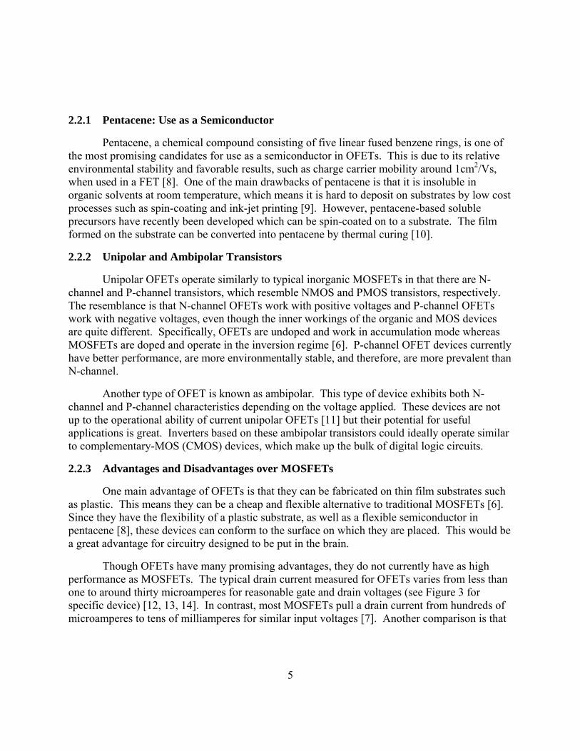
used displayed a carrier mobility of around 0.2 cm2/Vs and gate-oxide capacitance of 7.65nF/cm2. A typical gate voltage (Vg) to drain current (Id) curve is shown in Figure 3a. Figure 3b shows a corresponding drain-to-source voltage (Vds) to Id curve for varying gate voltages. These transistors were constructed on silicon wafers with a dual dielectric stack of thin silicon dioxide and BCB. Pentacene was the semiconductor in these devices and self-assembled monolayers were applied to the source and drain to enhance ambipolar characteristics. Complete description of these devices can be found in [10].
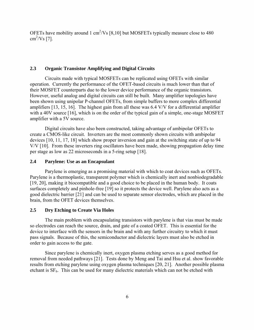
Several different amplification circuits were tested. The first was the common source amplifier. This geometry is the simplest because it utilizes only one transistor, but can achieve relatively large gains. By definition, the common source amplifier, as shown in Figure 4a, has the source connected to ground, the drain connected to a resistor, and the gate attached to a DC bias with a small AC signal riding on it. The other end of the drain resistor is
attached to a high voltage which supplies the source for the drain current. In this case, -50V was used since the ambipolar transistor
Figure 3: Typical characteristic curves of organic transistors used (a) Id-Vg (b) Id-Vds
8
used works best as p-type. Drain resistances used were varied from 1MΩ to over 20 MΩ to make up for the small drain currents. Both the output voltage at the drain and the input small signal were analyzed on an oscilloscope. However, since the input impedence of the scope was 10MΩ, on the same order as the drain resistances, a buffer was used to avoid excess loading. The buffer was an LM741CN opamp in the voltage follower configuration and adequately reduced the amount of current drawn from the circuit by the scope.
Figure 4b illustrates the cascode amplifier configuration which was also tested. This setup is similar to the common source but with a second transistor between the drain of the first transistor and the resistor. This second transistor is biased at a certain DC voltage, -50V in our tests, to increase the overall gain of the circuit.
Figure 4: Transistor amplifier topologies (a) common source (b) cascode
3.2 Etching Setup
In order to pattern via holes to connect the gates of an organic device to sensing electrodes, etching methods and rates had to be determined for the materials in the device. These materials include parylene-c, which acts as an encapsulant, along with benzocyclobutene (BCB) and spin-on-glass (SoG), which are used as dielectric materials in the transistors. SoG is a glass resin liquid mixture in the silicone family which helps the BCB stick to the device and spin-coat more evenly. It also effectively reduced leakage current between the gate and top electrodes. SoG was spin coated on substrates for 60 seconds at 3000 revolutions per minute then heated for 45 minutes at 200 degrees Celsius. Similarly, BCB was then spin coated on top at 3000 rpm for 30 seconds then cured at 290 degrees for 30 more seconds. A Specialty Coating Systems PDS2010 coater was used for vacuum deposition of parylene. The thickness of parylene on the
9
sample depended on the length of the process and the amount of the parylene monomer used. Typically somewhere between one and four microns were deposited on samples.
The etching process itself was performed on a Technics Planar Etch II parallel-plate Reactive Ion Etching device. This machine was capable of using the plasma of two gases, O2 and SF6, to etch samples. The O2 was used to etch parylene whereas SF6 was used to etch BCB and SoG. These organic transistor materials were applied to different substrates including glass, silicon wafer, and Kapton, a type of polyimide, in order to test their etching abilities. The depth of etching was measured using a Tencor Alpha Step 200 profilometer when possible. For some samples the thickness of the material was too small to be accurately measured using the profilometer. For this reason many samples were made using gold-covered silicon wafers and Kapton on which gold gates were deposited. Once the materials were coated and etched off these substrates, subsequent gold strips were deposited. The conductance between the original gold and top-layered gold was tested using the probe station. If the conductance was high between the two gold areas then it could be concluded that the intermediary substances were sufficiently etched.
4. Results and Analysis
4.1 Amplification
Based on the characteristics of the organic transistors, gains for the amplifier circuits were first predicted using standard FET equations. The following equation was used for the common source amplifier:
|Gain| = gmRd = μCox (|Vgs| - |Vt|)Rd
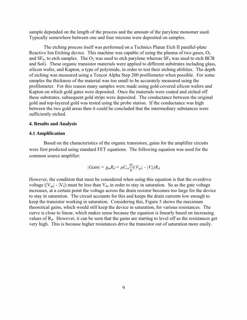
However, the condition that must be considered when using this equation is that the overdrive voltage (|Vgs| - |Vt|) must be less than Vds in order to stay in saturation. So as the gate voltage increases, at a certain point the voltage across the drain resistor becomes too large for the device to stay in saturation. The circuit accounts for this and keeps the drain currents low enough to keep the transistor working in saturation. Considering this, Figure 5 shows the maximum theoretical gains, which would still keep the device in saturation, for various resistances. The curve is close to linear, which makes sense because the equation is linearly based on increasing values of Rd. However, it can be seen that the gains are starting to level off as the resistances get very high. This is because higher resistances drive the transistor out of saturation more easily.
10
Figure 5: Calculated gain for increasing drain resistance
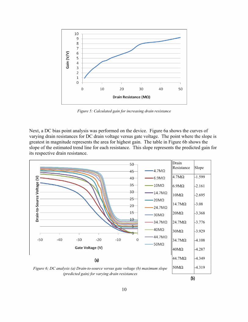
Next, a DC bias point analysis was performed on the device. Figure 6a shows the curves of varying drain resistances for DC drain voltage versus gate voltage. The point where the slope is greatest in magnitude represents the area for highest gain. The table in Figure 6b shows the slope of the estimated trend line for each resistance. This slope represents the predicted gain for its respective drain resistance.
Drain Resistance Slope
4.7MΩ -1.599
6.9MΩ -2.161
10MΩ -2.695
14.7MΩ -3.08
20MΩ -3.368
24.7MΩ -3.776
30MΩ -3.929
34.7MΩ -4.108
40MΩ -4.287
44.7MΩ -4.349
50MΩ -4.319 Figure 6; DC analysis (a) Drain-to-source versus gate voltage (b) maximum slope (predicted gain) for varying drain resistances
11
The Vds-Vg curves show that the range of highest slope gets shorter closer to zero as the resistance increases. This is because with a higher resistance, the voltage across the drain resistor increases more quickly and pushes the device out of saturation earlier. It can also be seen from Figure 6 that as resistance increases the predicted gain typically increases. This is expected from the calculations, as shown in Figure 5. Another similarity is that both sets of gain predictions appear to be leveling off at high resistances. The gain ceiling is much lower from the DC analysis, however. The calculated gains are based on traditional MOSFET calculations which do not exactly fit the OFETs. For instance, the mobility of organic devices tends to vary with the gat voltage, a phenomenon not accounted for in the calculations. The predicted gains from Figure 6 seem to predict the gains more realistically since they are based specifically on the devices that will be used.
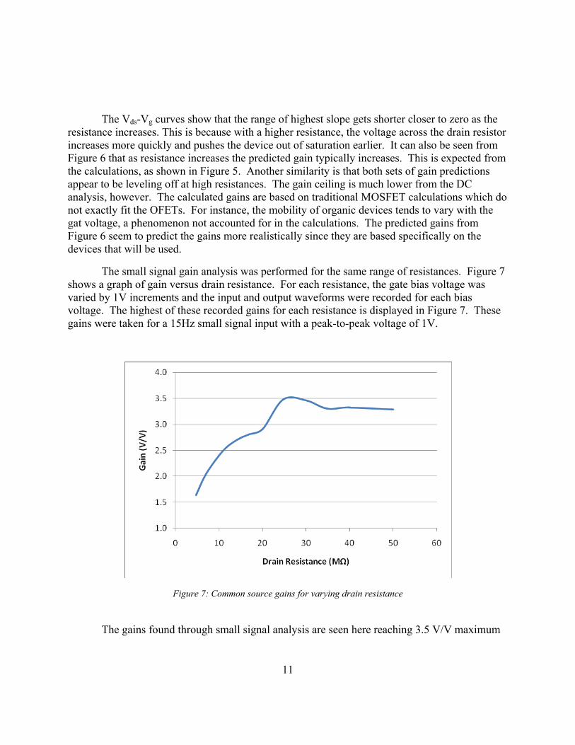
The small signal gain analysis was performed for the same range of resistances. Figure 7 shows a graph of gain versus drain resistance. For each resistance, the gate bias voltage was varied by 1V increments and the input and output waveforms were recorded for each bias voltage. The highest of these recorded gains for each resistance is displayed in Figure 7. These gains were taken for a 15Hz small signal input with a peak-to-peak voltage of 1V.
Figure 7: Common source gains for varying drain resistance
The gains found through small signal analysis are seen here reaching 3.5 V/V maximum
12
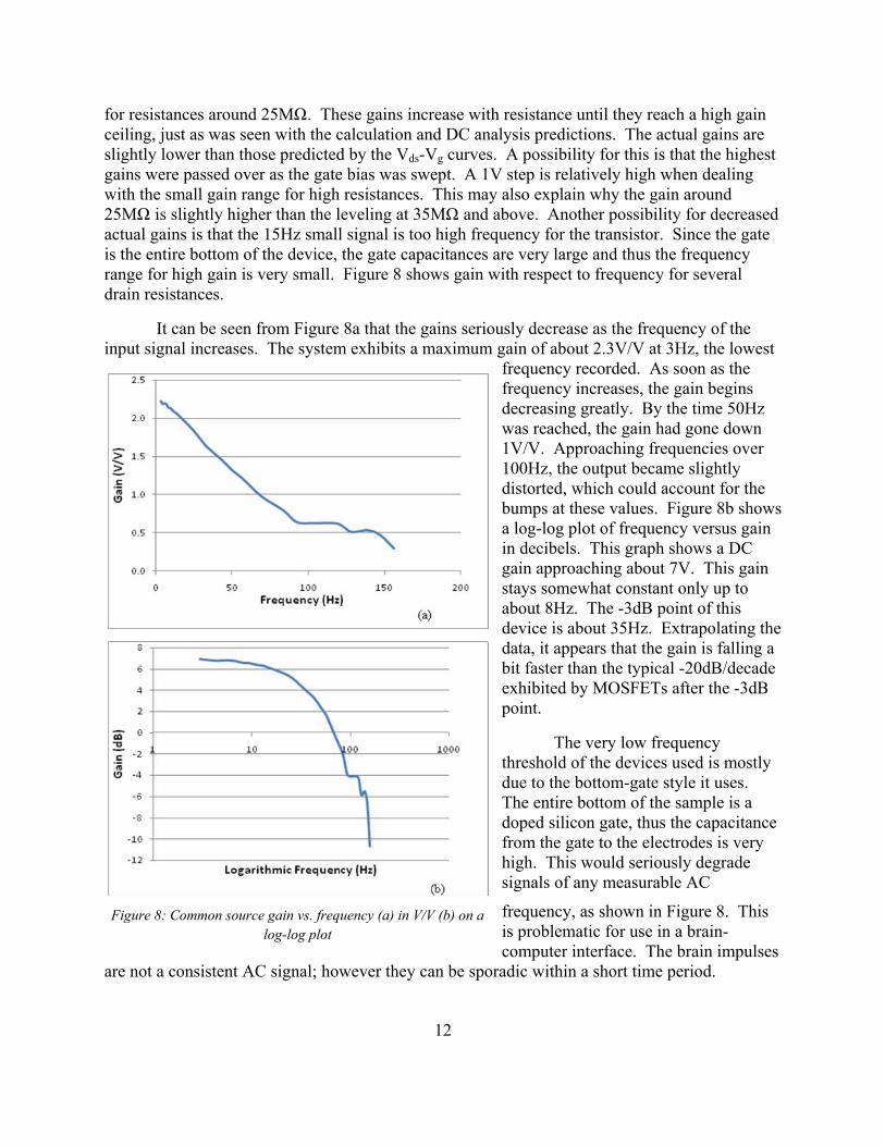
for resistances around 25MΩ. These gains increase with resistance until they reach a high gain ceiling, just as was seen with the calculation and DC analysis predictions. The actual gains are slightly lower than those predicted by the Vds-Vg curves. A possibility for this is that the highest gains were passed over as the gate bias was swept. A 1V step is relatively high when dealing with the small gain range for high resistances. This may also explain why the gain around 25MΩ is slightly higher than the leveling at 35MΩ and above. Another possibility for decreased actual gains is that the 15Hz small signal is too high frequency for the transistor. Since the gate is the entire bottom of the device, the gate capacitances are very large and thus the frequency range for high gain is very small. Figure 8 shows gain with respect to frequency for several drain resistances.
It can be seen from Figure 8a that the gains seriously decrease as the frequency of the input signal increases. The system exhibits a maximum gain of about 2.3V/V at 3Hz, the lowest
frequency recorded. As soon as the frequency increases, the gain begins decreasing greatly. By the time 50Hz was reached, the gain had gone down 1V/V. Approaching frequencies over 100Hz, the output became slightly distorted, which could account for the bumps at these values. Figure 8b shows a log-log plot of frequency versus gain in decibels. This graph shows a DC gain approaching about 7V. This gain stays somewhat constant only up to about 8Hz. The -3dB point of this device is about 35Hz. Extrapolating the data, it appears that the gain is falling a bit faster than the typical -20dB/decade exhibited by MOSFETs after the -3dB point.
The very low frequency threshold of the devices used is mostly due to the bottom-gate style it uses. The entire bottom of the sample is a doped silicon gate, thus the capacitance from the gate to the electrodes is very high. This would seriously degrade signals of any measurable AC
frequency, as shown in Figure 8. This is problematic for use in a brain-computer interface. The brain impulses
are not a consistent AC signal; however they can be sporadic within a short time period.
Figure 8: Common source gain vs. frequency (a) in V/V (b) on a log-log plot
13
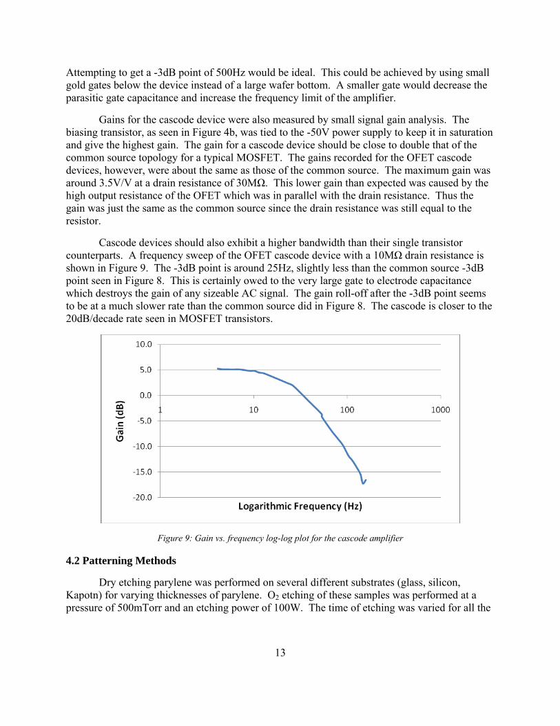
Attempting to get a -3dB point of 500Hz would be ideal. This could be achieved by using small gold gates below the device instead of a large wafer bottom. A smaller gate would decrease the parasitic gate capacitance and increase the frequency limit of the amplifier.
Gains for the cascode device were also measured by small signal gain analysis. The biasing transistor, as seen in Figure 4b, was tied to the -50V power supply to keep it in saturation and give the highest gain. The gain for a cascode device should be close to double that of the common source topology for a typical MOSFET. The gains recorded for the OFET cascode devices, however, were about the same as those of the common source. The maximum gain was around 3.5V/V at a drain resistance of 30MΩ. This lower gain than expected was caused by the high output resistance of the OFET which was in parallel with the drain resistance. Thus the gain was just the same as the common source since the drain resistance was still equal to the resistor.
Cascode devices should also exhibit a higher bandwidth than their single transistor counterparts. A frequency sweep of the OFET cascode device with a 10MΩ drain resistance is shown in Figure 9. The -3dB point is around 25Hz, slightly less than the common source -3dB point seen in Figure 8. This is certainly owed to the very large gate to electrode capacitance which destroys the gain of any sizeable AC signal. The gain roll-off after the -3dB point seems to be at a much slower rate than the common source did in Figure 8. The cascode is closer to the 20dB/decade rate seen in MOSFET transistors.
Figure 9: Gain vs. frequency log-log plot for the cascode amplifier
4.2 Patterning Methods
Dry etching parylene was performed on several different substrates (glass, silicon, Kapotn) for varying thicknesses of parylene. O2 etching of these samples was performed at a pressure of 500mTorr and an etching power of 100W. The time of etching was varied for all the
14
different samples in order to obtain adequate data. The etch rate of parylene under these conditions was found to be approximately 0.2μm/min using the profilometer. The samples measured on silicon and glass gave the best results for thickness etched. It was difficult to adequately measure Kapton-based samples under the profilometer due to the non-planarity of the Kapton surface.
BCB and SoG were etched with SF6 at 500mTorr as well, but the power typically used was 75W. These substances could not be measured well on the profilometer. The SoG was not etched by the SF6 well and thus would prove difficult for patterning via holes. BCB appeared to be etched, but could not be measured since it was only a few hundred nanometers to begin with.
5. Conclusions
Amplifying circuits were set up using pentacene-based organic transistors. Regular common source topologies exhibited gains up to 3.5V/V for resistances near 25MΩ. These gains were seen over about 10Hz. Cascode was also tested to find the same gains as common source with a slightly lower frequency drop. Parylene was etched using oxygen plasma and exhibited a rate of 0.2μm/min at 500mTorr and 100W. BCB and SoG were plasma etched using SF6, but SoG exhibited no useful etching and BCB appeared etched, but was not able to be measured.
6. Recommendations
The biggest difficulty for testing the amplifier circuits was doing so around a glove-box probe station. This limited the amount of devices to two and also inhibited testing to a certain degree. If devices could be patterned in the circuit form on a substrate using photolithography, higher level topologies could be tested. This would require all transistors as biases since resistors could not be easily put on a chip. This would also further investigate the ambipolar properties of the OFETs created for that purpose.
For the etching process, using a mask to add photoresist to a device in a hole-over-gate fashion could be attempted. This could be done on a transistor itself. After the etching an electrode could be deposited down the hole. The device could then be tested using the electrode as the gate access. This would show that the patterning methods are useful for application on the OFETs. Another possibility for future work on the etching is to use a polyimide dielectric as opposed to SoG and BCB, which were proven to difficult to etch. Polyimide dielectrics have been shown to produce devices with decent characteristics, and may be much easier to etch [22].
7. Acknowledgments
I would like Dr. Cherie Kagan, Dr. Jan Van der Spiegel, and Sangam Saudari of the University of Pennsylvania for their support and guidance for this project. I also want to thank David Kim and Yu Jen Lin for their help throughout the summer. Finally I am very grateful to the NSF for giving me the opportunity to experience research as part of the SUNFEST program.
15
References
[1] M. Berggren, A. Richter-Dahlfors, Organic Bioelectronics, Adv. Mat., 19 (2007) 3201-3213.
[2] R. A. Normann, Microfabricated Electrode Arrays for Restoring Lost Sensory and Motor Functions, 12th Int. Conf. on Solid State Sensors, Actuators, and Microsystems, 2 (2003) 959-962.
[3] H.M. Hamer, H.H. Morris, E.J. Mascha, M.T. Karafa, W.E. Bingman, M.D. Bej, R.C. Burgess, D.S. Dinner, N.R. Foldvary, J.F. Hahn, P. Kotagal, I. Najm, E. Wyllie, H.O. Lüders, Complications of Invasive Video-EEG Monitoring with Subdural Grid Electrodes, Neurology, 58 (2002) 97-103.
[4] J.J. Van Gompel, G.A. Worrell, M.L. Bell, T.A. Patrick, G.D. Cascino and C. Raffel et al., Intracranial Electroencephalography with Subdural Grid Electrodes: Techniques, Complications, and Outcomes, Neurosurgery, 63 (2008) 498–505.
[5] R. Ornstein, The Evolution of Consciousness: The Origins of the Way We Think, New York, Simon & Schuster, 1992, 63.
[6] J. Zaumseil, H. Sirringhaus, Electron and Ambipolar Transport in Organic Field-Effect Transistors, Chem. Rev., 107 (2007) 1296-1323.
[7] A. S. Sedra, K. C. Smith, Microelectronic Circuits, 4 (1998) 353-395.
[8] C. R. Kagan, A. Afzali, T. O. Graham, Operational and Environmental Stability of Pentacene Thin-Film Transistors, Appl. Phys. Lett. 86 (2005) 193505.
[9] A. Afzali, C. D. Dimitrakopoulos, T. L. Breen, High-Performance, Solution-Processed Organic Thin Film Transistors from a Novel Pentacen Precursor, J. Am. Chem. Soc., 124 (2002) 8812-8813.
[10] S. R. Saudari, P. R. Frail, C. R. Kagan, Ambipolar Transport in Solution-Deposited Pentacene Transistors Enhanced by Molecular Engineering of Device Contacts, Appl. Phys. Lett., 95 (2009) 023301.
[11] T. B. Singh, P. Senkarabacak, N. S. Sariciftci, A. Tanda, C. Lackner, R. Hagelauer, G. Horowitz, Organic Inverter Circuits Employing Ambipolar Pentacene Field-Effect Transistors, Appl. Phys. Lett. 89 (2006) 033512.
[12] M. G. Kane, J. Campi, M. S. Hammond, F. P. Cuomo, B. Greening, C. D. Sheraw, J. A. Nichols, D. J. Gundlach, J. R. Huang, C. C. Kuo, L. Jia, H. Klauk, T. N. Jackson, Analog and Digital Circuits Using Organic Thin-Film Transistors on Polyester Substrates, IEEE Electron Dev. Lett., 21 (2000) 534-536.
16
[13] D. M. Binkley, N. Verma, R. L. Crawford, E. Brandon, T. N. Jackson, Design of an Auto-Zeroed, Organic Thin-Film Field-Effect Transistor Amplifier for Sensor Applications, Proc. Of SPIE – The Int. Soc. For Opt. Eng., 5522 (2004) 41-52.
[14] R. Brederlow, S. Briole, H. Klauk, M. Halik, U. Zschieschang, G Schmid, J.-M. Gorriz-Saez, C. Pacha, R. Thewes, W. Weber, Evaluation of the Performance Potential of Organic TFT Circuits, Int. Solid-State Circ. Conf., 21 (2003) 21.6.
[15] N. Gay, W.-J. Fischer, OFET-Based Analog Circuits for Microsystems and RFID-Sensor Transponders, IEEE Polytronic 2007 Conf., 6 (2007) 143-148.
[16] M. Takamiya, T. Sekitani, Y. Miyamoto, Y. Noguchi, H. Kawaguchi, T. Someya, T. Sakurai, Design for Mixed Circuits of Organic FETs and Plastic MEMS Switches for Wireless Power Transmission Sheet, Int. Conf. on IC Des. and Tech., 4299565 (2007) 168-171.
[17] T. D. Anthopoulos, D. M. de Leeuw, S. Setayesh, E. Cantatore, C. Tanase, P. W. M. Blom, J. C. Jummelen, Integrated Complementary-Like Circuits Based on Organic Ambipolar Transistors, Mater. Res. Soc. Symp. Proc., 871E (2005) I11.9.1-I11.9.6.
[18] H. Klauk, M. Halik, U. Zschieschang, G. Schmid, W. Radlik, Polymer Gate Dielectric Pentacene TFTs and Circuits on Flexible Substrates, Int. Electron Dev. Meet., 22.1 (2002) 557-560.
[19] T. Y. Chang, V. G. Yadav, S. De Leo, A. Mohedas, B. Rajalingam, C.-L. Chen, S. Selvarasah, M. R. Dokmeci, A. Khademhosseini, Cell and Protein Compatibility of Parylene-C Surfaces, Langmuir, 23 (2007) 11718-11725.
[20] E. Meng, Y.-C. Tai, Parylene Etching Techniques for Microfluidics and BioMEMs, IEEE 2005 MEMS Conf., 18 (2005) 568-571.
[21] J.-M. Hsu, L. Reith, R. A. Normann, P. Tathireddy, F. Solzbacher, Encapsulation of an Integrated Neural Interface Device with Parylene C, IEEE Trans. On Biomed. Eng., 56 (2009) 23-29.
[22] H. Kawaguchi , T. Sakurai, High Mobility of Pentacene Field-Effect Transistors with Polyimide Gate Dielectric Layers, Appl. Phys. Lett., 84 (2004) 3789-3791.


![[Chapter III] Basic Knowledge of Discrete Semiconductor ......transistors (IGBTs) Power transistors (2SAxx,2SBxx,2SCxx,2SDxx, TTAxx,TTBxx,TTCxx,TTDxx) Types of Transistors Transistors](https://img.pdfslide.us/doc/110x75/5e766014341a1a707d5f4c34/chapter-iii-basic-knowledge-of-discrete-semiconductor-transistors-igbts.jpg)