Embed Size (px)
Citation preview

CIRCUITS LABORATORY
EXPERIMENT 2
The Oscilloscope and Transient Analysis 2.1 Introduction In the first experiment, the utility of the DMM to measure many simple DC quant-
ities was demonstrated. However, in the vast majority of electrical circuits having
practical use, the quantities of interest vary with time. While the DMM can be used
to make measurements on such signals (and you will be introduced to its use for this
purpose in future experiments), it is often desired to visually observe such signals as a
function of time. By converting time into distance on the face of a cathode ray tube
(CRT), signals much faster than the human eye can follow can be displayed. The
resulting instrument is an oscilloscope whose unique features are invaluable to the
electrical engineer in activities that range across the whole spectrum of the
profession. This experiment describes the oscilloscope and illustrates its use with
several exercises involving series RC, RL, RLC circuits plus an electrical relay.
2 – 1

2.2 Objectives At the end of this experiment, the student will be able to: (1) use the oscilloscope to measure the voltage, period, and rise/fall times of periodic signals, (2) adjust the oscilloscope probe so that it gives optimum response at high
frequencies (3) sketch the equivalent circuit of the oscilloscope plus probe connection for both the 1x and l0x probes, (4) choose the best probe to use for a given signal of interest, (5) explain how the equipment in our lab is grounded, (6) analyze the transient response of series RC, RL, and RLC circuits, (7) design a circuit to determine the coil inductance of an electrical relay, and (8) use the oscilloscope to measure the switching times of a Single Pole Single Throw (SPST) electrical relay. 2.3 Theory 2.3.1 General Considerations The cathode ray tube (CRT) is one of the most useful electronic devices. It is familiar to all of us in its everyday use as a television display and also as a device for displaying alphanumeric information when used as a computer monitor. Usage of the term 'cathode ray' dates from Faraday (1865) who observed luminescence between electrodes in a rarefied atmosphere. A number of early day scientists including 2 - 2

Crookes and Thomson worked to establish that 'cathode rays' were actually electrons moving at high speed in a vacuum. When the moving electrons impinge on a 'phosphor' material, in particular zinc sulfide, the electron kinetic energy is partially converted to light energy and the phosphorescence produced can be utilized for display purposes. The term 'phospho- rescence' refers to the production of light after excitation as contrasted to 'fluores- cence' which implies light production during excitation. Most of the light output from CRTs is due to phosphorescence. Phosphors differ widely in their 'persistence'; a P16 phosphor decays to the 10% level within one microsecond while a P26 phos- phor requires 16 seconds to reach this level. The efficiency with which a CRT converts electrical energy to light is rather good, perhaps 50 lumens/Watt for some phosphors, and may be two or more times larger than a good incandescent lamp. A moving electron experiences a force from both electric and magnetic fields. This is the 'Lorentz force' of amount F = q(E + v x B) (2.1) This leads to two types of CRTs, which differ in their deflection method. Tubes used for TV display and computer monitors employ magnetic deflection of the electron beam while tubes for oscillographic purposes use electrostatic deflection. The basic structure in the two cases is shown in Figure 2.1. Several reasons exist for this preference in the two applications. For one, mag- netic deflection allows a substantially wider linear deflection angle to be realized which is desirable for large screen displays, as in a television receiver. On the other 2 - 3

hand producing an appropriate, relatively large, deflection current and forcing it through deflection coils requires inordinately high voltages at higher frequencies and indeed may not be possible at frequencies above which the deflection coil is self resonant. Commonly then, tubes for oscillographic purposes are relatively long and narrow so that precision in the amount of deflection per unit voltage applied to the deflection plates is obtained. The electron beam itself is produced by a heated cathode which is held at a negative potential, some several hundred volts below the potential of an acceler- ating electrode. Beam focusing also takes place in the accelerating electrode after which the beam passes through the deflection plates. Further acceleration occurs due to a large potential difference (the 'high voltage supply') between the phosphor screen and the accelerating electrode. Depending on the secondary emission charac- teristic of the phosphor, this potential may range up to 20 kV. Generally speaking, 2 - 4

there is a range of electron energies where, if the electrons impinge on a phosphor, more electrons are ejected from the phosphor than impinge upon it. Consequently, a potential difference cannot be maintained between phosphor and cathode that exceeds the upper extreme of the range over which the secondary emission ratio exceeds unity. Although screen brightness can be varied by adjusting the phosphor potential, more commonly the intensity of the beam is varied by a grid operated negative relative to the cathode so as to reduce or cut off the number of electrons reaching the phosphor per unit time. This grid represents the 'z-axis' input, as it is commonly called in oscillography, and allows intensity modulation of the CRT with an external electrical signal. The main function of an oscilloscope is to display, as a function of time, the waveform of a voltage applied to its terminals. Since the deflection sensitivity of a CRT, defined as the deflection plate voltage required for the beam to trace out unit distance on the face of the CRT, is on the order of 30 Volts/inch, substantial amplification of the input signal is required to obtain a usable deflection and this is obtained via the vertical amplifier in the oscilloscope. Figure 2.2 (a) shows a partial block diagram of a conventional analog oscilloscope. The diagram omits such details as attenuators and some of the switching circuits. Within the last few years, the analog oscilloscope, as described above, has been largely displaced by the ‘digital oscilloscope’. In contrast to the analog scope, which displays its trace as it is generated, the digital scope collects data for the entire waveform and then displays it. Figure 2.2 (b) shows a block diagram of a digital ` 2 - 5

oscilloscope. The function of the vertical system in this figure is to adjust the amplitude of the signal to place it in the range of the analog-digital converter in the
acquisition system block. In the acquisition system the analog-digital converter samples the signal at discrete points in time and converts the signals voltage at these points to digital values called sample points. These are then stored in memory to be later displayed. The horizontal systems sample clock determines how often the converter takes a sample. The rate at which the clock operates is called the sample rate and is measured in samples/second. When stored in memory, the sample points become waveform points. More than one sample point may make up a waveform point using, for example, averaging methods. Together, the waveform points make 2 - 6
Figure 2.2 (a): Partial block diagram of a conventional analog oscilloscope.

up one waveform record. The number of waveform points used to make a waveform record is called the record length. The trigger system determines the start and stop points of the record. The display receives these record points after they are stored in memory.
Fig. 2.2 (b): Digital Oscilloscope Block Diagram As you will notice when you begin this experiment, the oscilloscope is a com- plicated instrument with a wide range of features. In this course, you will use the Agilent 54622D Digital Oscilloscope. 2 – 7

2.3.2 Making Measurements Using the Oscilloscope The input impedance of the vertical and horizontal amplifiers (see Figure 2.2) of a typical oscilloscope is high. This serves to minimize the loading of a circuit under test and the consequent distortion of the observed waveform. In our lab oscilloscopes, the input impedance can be represented by an equivalent circuit which is a 1 MΩ resistor in parallel with a 14 pF capacitor for both the vertical and horizontal amplifiers. This equivalent circuit is shown in Figure 2.3, where vi(t) is the waveform at the input terminals of the oscilloscope. Note that this input impedance can cause objectionable noise and interference on the display if measurements are made on a high impedance circuit via unshielded wires. Furthermore, ordinary coaxial cable has a capacitance on the order of 14 pF/ft so shielded cable effectively adds capacitance in parallel with the 14 pF inherent in
the instrument. Nevertheless, if the impedance level of the circuit being measured is low, say less than 10 kΩ, and if the rise and fall times being measured are not too 2 - 8
14 pf

fast, say greater than roughly lμs, then shielded cable or a “lx Probe” may be used to connect the oscilloscope to the circuit. If the circuit conditions lie outside these ranges, then the “l0x probe” gives better performance at some sacrifice in sensitivity. The equivalent circuit of the l0x probe is shown in Figure 2.4. The l0x probe presents an effective impedance to the circuit of about 10 MΩ in parallel with less than 14 pF of capacitance (depending on the capacitance of the connectors and the probe wire) and so introduces less error in the measuring process than does the 1x probe. It should be noted though that the sensitivity of the l0x probe is only one tenth of that of a 1x probe. Most l0x probes provide an adjustment so that the capacitance, C, can be varied to allow optimum scope response at high frequencies where the capacitive portion of the input impedance dominates. All oscilloscopes provide a calibration signal for checking if the l0x probe has been properly adjusted. To ensure optimum measurement
2 - 9
14 pf

accuracy, always check that the l0x probes are critically compensated before making any measurements. In many cases, little error is incurred in a measurement if ordinary banana plug terminated wires are used to connect the scope to a circuit. Generally, if the signal level is large enough so that the noise introduced by the unshielded wires is negligible, the convenience of banana plug wires may justify their use. 2.3.3 RC Transient Circuit Analysis In this section, we will review the fundamentals of RC transient circuit analysis. Analysis of this sort is important for a number of reasons; for example, many non- linear devices used in switching circuits can be modeled in terms of RC circuits. Also, the equivalent circuits of the wires, connectors, and equipment used to measure cir- cuit behavior are RC circuits and it is this situation with which we will be primarily concerned in this experiment. Consider the circuit shown in Figure 2.5. This circuit consists of a resistor R
in series with an ideal capacitor C. We shall assume that v(t) is a square wave 2 - 10

switching between 0 and +V volts with a period T. Using Kirchhoff's voltage law, we can write the following equation. (2.2) Making use of the voltage-current relationship for a capacitor, namely, that iC(t) = CdvC(t)/dt, and then rearranging terms, this equation becomes (2.3) From your introductory course in circuit analysis, recall that this equation can easily be solved for vC(t) by separating the variables (vC(t) and t) for any interval of time for which v(t) is constant. (That is, for 0 < t < T/2, v(t) is equal to +V, and for T/2 < t < T, v(t) is equal to 0.) This analysis is left as an exercise for the student. A general approach to analyzing circuits of this type can be obtained if one considers the initial and final value of the capacitor voltage over any interval of time for which v(t) is constant. Suppose that at time t0 the voltage v(t) switches from Va to Vb and remains equal to Vb until time t1. From your introductory circuit analysis course, recall that it was shown that the general solution for vC(t) for times between t0 and t1 is given by , (2.4) where τ = RC, the RC circuit time constant. In this equation, VI is the initial value of the capacitor voltage (i.e., the value at t0), and VF is the final value of the capacitor voltage assuming the input voltage remains constant (i.e., the value at t = ∞). Note 2 - 11
.0)()()( =++− tvRtitv CC
)()()( tvtvdt
tdvRC CC =+
τ)0(
)()(tt
eVVVtv FIFC
−−
−+=

that if the half-period (T/2) of the square wave is sufficiently long, the value of vC(t)
will come "close to" the final value VF before the value of v(t) changes again. The
definition of "close to" is of course arbitrary, but we will take this
term to mean within 1 % of the final value. It can be shown that it takes
roughly 5 time constants (5τ) for vC(t) to come within 1 % of its final value, so we
assume that vC(t1) = VF when (t1 - t0) > 5τ.
To find the values of VF and VI, first recall that the voltage across a capacitor cannot change instantaneously with time. Also, clearly if v(t) is constant for a long time, then iC(t) = 0, and hence vC(t) = v(t). Therefore, one can see that at time the value of vC(t) is Va, and, since the voltage across a capacitor cannot change instan- taneously with time, the value of vC(t) at t0
+ is also Va. Therefore, VI = Va. Similarly, one can argue that VF = Vb at t1, provided (t1 - t0) > 5τ. Thus, Equation (2.4) becomes
(2.5) Using this general solution, we can directly write down the expression for vC(t) when v(t) is a square wave switching between 0 and +V volts with a period T. If the condition 5τ < (T/2) is satisfied, then the capacitor voltage is for 0 < t < T/2, and (2.6) for T/2 < t < T . (2.7) If one wished to go further and obtain an expression for the current iC(t), it could easily be obtained using the voltage-current relationship for the capacitor. 2 – 12
−0t
.)()()( 0
τtt
babC eVVVtv−−
−+=
)1()( /τtC eVtv −−=
τ/)2/()( TtC Vetv −−=

2.3.4 Probe Effects In the first experiment, we learned that when using the DMM to measure voltage, it is possible to affect the voltage being measured. This occurs because the (DC) input resistance of the DMM is finite, which allows current to flow through the DMM, thereby changing the voltage being measured. In a similar way, the oscilloscope does not present an infinite impedance to the circuit under test, so its use in measuring a voltage waveform often alters the waveform being measured. Furthermore, the impedance presented to the circuit when using the lx probe and the l0x probe is not the same, so these two probes will alter the waveform being measured in different ways. In this section, we will quantify the way in which these two probes can alter the waveform under test.
2.3.4.1 lx Probe Consider the circuit shown in Figure 2.6 having a scope, probe and external resistor Rex connected in series to a 33120A function generator. Now, suppose that the function generator has been set to produce a square wave and that the 1x scope probe has been used to connect the resistor to Channel 1 input of the oscilloscope.
2 - 13
Figure 2.6 Circuit Connection Using 1x Probe
Probe
Fcn Gen Grounding Wire to Scope33120A Function

An equivalent circuit for this connection is shown in Figure 2.7. The output of Figure 2.7: Equivalent circuit for the 1x probe connection. the signal generator is represented by an ideal voltage source vsig(t) and an internal
generator source resistance Rsig. The input impedance of the scope is represented by a
1MΩ resistor in parallel with a 14 pF capacitor. The unknown capacitance intro-
duced by the wires and connectors is represented by the capacitor labeled Cp. Note
that CP for a 1x Probe is approximately 60 pF. Finally, vi(t) is the input voltage into
the scope and v0(t) is the resultant voltage which is displayed on the CRT.
The equivalent circuit shown in Figure 2.7 can be simplified as shown in Figure
2.8. Note that Rt = (Rsig + Rex) and Ct = (14 pF + Cp). Notice also that this is an RC
circuit driven by the input signal vsig(t.)
2 - 14
Figure 2.8: Simplification of the equivalent circuit for the 1x probe connection.
1
Probe
1
14 pF

The equivalent circuit for the 1x probe can be further simplified by redrawing it as
shown in Figure 2.9 (a) and then taking the Thevenin's equivalent circuit across the
capacitor Ct, i.e., across Terminals a and b, as shown in Figure 2.9 (b).
Figure 2.9: Further simplification of the equivalent circuit of the 1x probe connection: (a) After interchanging the capacitor and the 1 MΩ resistor, and (b) after taking the Thevenin equivalent circuit across the capacitor.
The Thevenin's equivalent circuit shown in Figure 2.9 (b) is obtained as a result,
where:
(2.8) and . (2.9) In the above equations, vT(t) and RT represent the Thevenin voltage and resistance, respectively. The circuit in Figure 2.9 (b) is a series RC circuit, and it follows that the time constant of this circuit is given by τ = RTCt. Assuming vsig(t) is a square wave switching between 0 and +V volts with a period T, it can be shown that if T/2 > 5τ, then the voltage across the capacitor during the positive half cycle when vsig(t) = V is given by for 0 ≤ t ≤ T/2. (2.10) 2 - 15
,)(1
1)( tvRM
Mtv sigt
T ⎟⎟⎠
⎞⎜⎜⎝
⎛+ΩΩ
=
Ω+Ω
=Ω=MRMRMRR
t
ttT 1
)1)((1||
)1(1
1)(0τt
t
eRM
MVtv−
−⎟⎟⎠
⎞⎜⎜⎝
⎛+ΩΩ
=

Similarly, the voltage across the capacitor during the negative half cycle when Vsig(t) = 0 is given by for T/2 ≤ t ≤ T . (2.11) Assuming that Rsig = 50Ω, Ct = 74 pF (i.e., Cp = 60 pF), and vsig(t) is the square wave defined above, one can then determine the expression for v0(t) for 0 ≤ t ≤ T. It follows that this expression represents the "expected" waveform for v0(t). Vari- ations in the actual waveform will result from any additional stray capacitance and resistanceintroduced by the wires and connectors. 2.3.4.2 10x Probe Again consider the series circuit shown in Figure 2.6, but suppose now that the l0x
probe has been used to connect the resistor Rex to the Channel 1 input of the scope.
Note that the digital scope recognizes that a 10x probe is connected and applies a gain
of 10 to compensate for the voltage divider effect of the 9 MΩ resistance of the 10x
probe. As before, the function generator has been set to produce a square wave.
Figure 2.10: Equivalent Circuit for the l0x Probe Connection.
2 – 16
τ/)2
(
0 11)(
Tt
t
eRM
MVtv−−
⎟⎟⎠
⎞⎜⎜⎝
⎛+ΩΩ
=
vi(t)
+ 10
14 pF

An equivalent circuit of this connection is shown in Figure 2.10. In this case, the l0x probe introduces an additional capacitor and resistor as shown previously in Figure 2.4. The capacitor Cp again represents the stray capacitance introduced by the connectors and the probe wire. If Cp and the 14 pF scope input capacitance are combined in parallel, then the equivalent circuit of Figure 2.11 results. Figure 2.11: Simplification of the equivalent circuit of the l0x probe connection. As mentioned previously, before using the l0x probe, it is important that it be critically compensated. It can be shown that when the l0x probe is critically compensated, the following condition must be satisfied: (9 MΩ) C = 1 MΩ (Cp + 14 pF). (2.12) This means that when we critically compensate the l0x probe, we are adjusting C so that (2.13) With C equal to this value, it can he shown using phasor analysis that the circuit 2 - 17
914 pFC
C p +=
(Cp + 14 pF)

in Figure 2.11 can be replaced with the equivalent circuit in Figure 2.12, where Ct = (Cp + 14 pF) / 10. Note that CP for the 10x probe is approximately 136 pF.
Figure 2.12: Simplification of the equivalent circuit of the l0x probe connection when the probe is compensated.
We now have an equivalent circuit for the l0x probe connection, which can be further simplified and analyzed in the same manner as the lx probe connection discussed previously. It follows that the circuit in Figure 2.12 can be simplified to the circuit given in Figure 2.13 (a) where Rt = (Rsig + Rex). This circuit can be
(2) (b) Figure 2.13: Further simplification of the equivalent circuit of the l0x probe connection: (a) After combining the signal generator resistance with the external resistor, and (b) after taking the Thevenin equivalent circuit across the capacitor. further simplified as shown in Figure 2.13 (b) by taking the Thevenin equivalent circuit across the capacitor, where 2 - 18
(a)
vi +
10

(2.14) and . (2.15) One can again solve for the expected waveform v0(t) using this equivalent circuit and assuming that Ct = 15 pF corresponding to CP = 136 pF. 2.3.5 Grounding of Electrical Equipment This section provides a brief introduction on how electrical equipment is grounded. Grounding is an important consideration in safety, and it is also one of the important ways to minimize noise. Furthermore, grounding is a critical consideration when configuring test equipment to make even the simplest of measurements. Figure 2.14 shows the standard three-wire AC distribution system that is used for electrical equipment.
Figure 2.14: Three-lead distribution system.
2 - 19
)(10
10)( tvRM
Mtv sigt
T ⎟⎟⎠
⎞⎜⎜⎝
⎛+ΩΩ
=
Ω+Ω
=Ω=MRMRMRR
t
ttT 10
)10)((10||
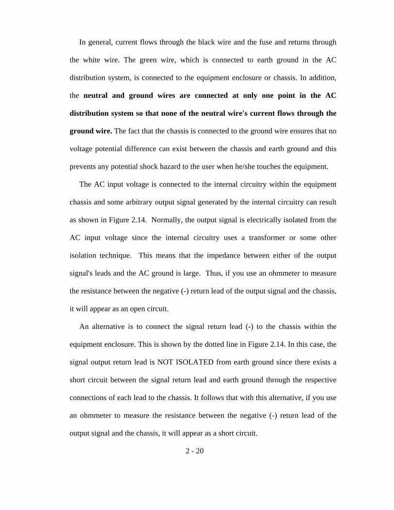
In general, current flows through the black wire and the fuse and returns through
the white wire. The green wire, which is connected to earth ground in the AC
distribution system, is connected to the equipment enclosure or chassis. In addition,
the neutral and ground wires are connected at only one point in the AC
distribution system so that none of the neutral wire's current flows through the
ground wire. The fact that the chassis is connected to the ground wire ensures that no
voltage potential difference can exist between the chassis and earth ground and this
prevents any potential shock hazard to the user when he/she touches the equipment.
The AC input voltage is connected to the internal circuitry within the equipment
chassis and some arbitrary output signal generated by the internal circuitry can result
as shown in Figure 2.14. Normally, the output signal is electrically isolated from the
AC input voltage since the internal circuitry uses a transformer or some other
isolation technique. This means that the impedance between either of the output
signal's leads and the AC ground is large. Thus, if you use an ohmmeter to measure
the resistance between the negative (-) return lead of the output signal and the chassis,
it will appear as an open circuit.
An alternative is to connect the signal return lead (-) to the chassis within the equipment enclosure. This is shown by the dotted line in Figure 2.14. In this case, the signal output return lead is NOT ISOLATED from earth ground since there exists a short circuit between the signal return lead and earth ground through the respective connections of each lead to the chassis. It follows that with this alternative, if you use an ohmmeter to measure the resistance between the negative (-) return lead of the output signal and the chassis, it will appear as a short circuit. 2 - 20

If the signal return leads of two instruments are NOT ISOLATED from chassis
ground, this results in both leads being connected together through the green ground
wire of the AC distribution system as illustrated by examining Figure 2.15 (a). On
the other hand, if the signal return lead of one of the instruments is ISOLATED, i.e.,
it is not connected internally to the chassis, then the return leads are not connected
through the ground wire as illustrated in Figure 2.15 (b).
In the Bryan Hall, Room 316 laboratory, the 33120A Function Generator output is
not internally grounded whereas the Digital Scope input is internally grounded as
shown in figure 2.15 (b), so a reference wire must be connected between the Function
Generator's (-) signal terminal and earth ground in order for the Digital Scope to be
able to measure signals. This results in a ground path equivalent to that shown in
Figure 2.15 (a).
(a) (b) Figure 2.15: Illustration of a instrument grounds and signal return leads. 2 - 21
Vout
Vin Vin
Vout
Vin
Vout
Vin

The DMM's signal return lead is isolated from chassis ground and thus a large
impedance exists between this lead and chassis ground or the signal return leads of
both the function generator and the scope.
Whenever the signal return lead is NOT ISOLATED from chassis ground, which
is the case for the Digital Scope, care must be taken when connecting the instrument
at any point in the circuit to make a measurement since you could be shorting the
connected point in the circuit to chassis ground without realizing it. This is best
understood by considering the circuit shown in Figure 2.16, which is assembled for
test purposes using the circuit of Figure 2.17
Figure 2.16: RC circuit used to demonstrate the oscill- oscope measurement problems that can occur when grounding is not properly understood. 2 - 22
b a

Figure 2.17: Faulty Connection of the oscilloscope. As shown, the scope leads are connected across R1 in order to observe the voltage
vR1(t). In this case, the result is that the components R2 and C are effectively
removed from the circuit once the negative return lead of the scope is connected to
node b of the circuit. This is due to the fact that node b is now connected to the return
lead of the function generator through the scope chassis, the AC ground wire, and the
function generator ground wire as illustrated by the dotted line. The equivalent circuit
resulting from connecting the scope in this manner is shown in Figure 2.18.
Figure 2.18: Equivalent circuit resulting from the connection in Figure 2.17 2 - 23
a
b a

One way to correct this problem is to reconfigure the circuit such that one side of R1 is connected to the negative return lead of the function generator (or chassis ground). This is illustrated in Figure 2.19. It follows that the scope always Figure 2.19: Reconfiguration of the RC circuit so that the voltage across R1 can be measured with the oscilloscope. measures the voltage differential between its positive lead (+) and chassis ground.
This explains why you don't even have to connect the negative lead (-) of the scope
when making measurements on circuits that use the 33120A Function Generator
provided that its signal return line is grounded. On the other hand, special care must
be taken when measuring the voltage across a component when using the scope so
that you don't short out components and modify the resultant operation of the circuit
you are trying to measure. This is achieved by always having one side of the
component connected to chassis ground when connecting the scope across it.
An alternative approach to measuring the voltage across R1 without reconfiguring
the circuit is to employ the Digital Oscilloscope's "Math Function" feature. This
feature can be used to obtain the difference between two waveforms. To do this,
consider the circuit connection shown in Figure 2.20. From the above discussion,
2 - 24
vT
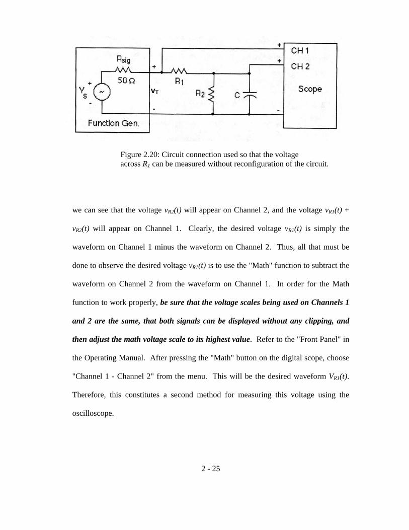
Figure 2.20: Circuit connection used so that the voltage across R1 can be measured without reconfiguration of the circuit.
we can see that the voltage vR2(t) will appear on Channel 2, and the voltage vR1(t) +
vR2(t) will appear on Channel 1. Clearly, the desired voltage vR1(t) is simply the
waveform on Channel 1 minus the waveform on Channel 2. Thus, all that must be
done to observe the desired voltage vR1(t) is to use the "Math" function to subtract the
waveform on Channel 2 from the waveform on Channel 1. In order for the Math
function to work properly, be sure that the voltage scales being used on Channels 1
and 2 are the same, that both signals can be displayed without any clipping, and
then adjust the math voltage scale to its highest value. Refer to the "Front Panel" in
the Operating Manual. After pressing the "Math" button on the digital scope, choose
"Channel 1 - Channel 2" from the menu. This will be the desired waveform VR1(t).
Therefore, this constitutes a second method for measuring this voltage using the
oscilloscope.
2 - 25
vT
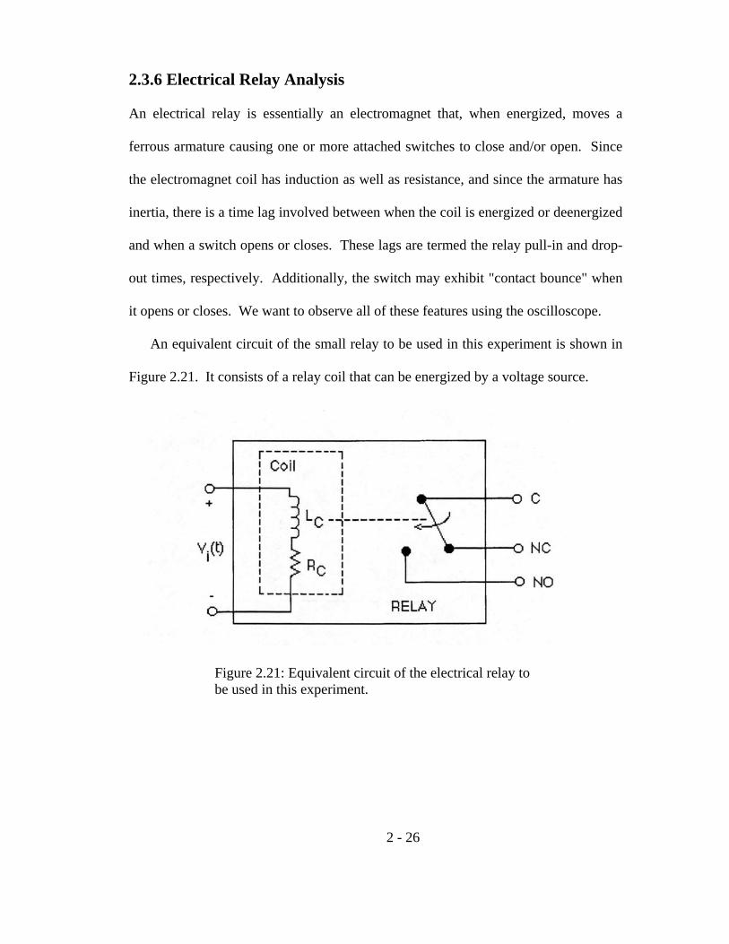
2.3.6 Electrical Relay Analysis An electrical relay is essentially an electromagnet that, when energized, moves a
ferrous armature causing one or more attached switches to close and/or open. Since
the electromagnet coil has induction as well as resistance, and since the armature has
inertia, there is a time lag involved between when the coil is energized or deenergized
and when a switch opens or closes. These lags are termed the relay pull-in and drop-
out times, respectively. Additionally, the switch may exhibit "contact bounce" when
it opens or closes. We want to observe all of these features using the oscilloscope.
An equivalent circuit of the small relay to be used in this experiment is shown in
Figure 2.21. It consists of a relay coil that can be energized by a voltage source.
Figure 2.21: Equivalent circuit of the electrical relay to be used in this experiment. 2 - 26

The relay coil is represented by an equivalent circuit consisting of an ideal
inductor LC, which represents the inductance of the coil, in series with a resistor RC,
which represents the resistance of the coil windings. When no excitation current is
flowing in the coil, the relay is de-energized and the switch is in the Normally Closed
(NC) position which results in a short circuit between the Common (C) switch contact
and the NC contact. When excitation current exists in the coil, the relay is energized
and the switch moves to the Normally Open (NO) position, which results in a short
circuit between the C contact and the NO contact.
2.3.7 RL Transient Circuit Analysis First, the coil resistance and inductance will be determined. The coil resistance can be
measured directly using the DMM as an ohmmeter. In order to find the value of the
inductance, an R-L circuit must be designed and used to measure the necessary
parameters.
Figure 2.22: Series R-L circuit,
Consider the circuit shown in Figure 2.22 above, which consists of a resistor R in
series with an ideal inductor L. Assuming v(t) is a square wave switching between 0
2 - 27

and V volts with a period T, it follows that if 5τ < (T / 2), the inductor current is
for 0 ≤ t ≤ T / 2, and (2.16) for T / 2 ≤ t ≤ T (2.17) where τ is the time constant of the R-L circuit and is given by τ = L/R. (2.18) The above result can be obtained using the same method that was used to derive the solution for the RC circuit. That is, suppose that at time t0 the voltage v(t) switches from Va to Vb and stays at the value Vb until time t1. Then, assuming that 5τ < (t1 – t0), the current in the inductor for t0 < t < t1 is given by (2.19) In this equation, II is the initial value of the inductor current (i.e., iL(t) at time t0) and IF is the final value of the inductor current (i.e., iL(t) at time t = ∞). Therefore, in order to write down the results given in Equations (2.16) and (2.17), all that we need
to do is compute the initial and final values of the inductor current and plug these
values into Equation (2.19).
It can also be shown that if tr is the 10% to 90% rise time of the signal, then tr = 2.2(τ) . (2.20) Similarly, if tf is the 90% to 10% fall time of the signal, then
tf = 2.2(τ) . (2.21) 2 - 28
)1()( / τtL e
RVti −−=
τ/)2/()( TtL e
RVti −=
τ)( 0
)()(tt
FIFL eIIIti−−
−+=

It follows that if we could measure tr or tf of iL(t), the value of the inductance can be determined from Equation (2.20) or Equation (2.21). Unfortunately, the oscilloscope will only enable us to measure and observe voltage signals. Now, the voltage across the resistor R is given by vR(t) = R iL(t) , (2.22) and it follows that the voltage across R is directly proportional to the current through the inductor and thus the rise and fall times of this voltage will be the same as the rise and fall times of the current. In developing the design of the required circuit, an external resistor must be added
in series with the relay coil so that the rise tr and fall time tf of the voltage can be
measured across this resistor using the oscilloscope. The external resistor must be
added because there is no way to measure the voltage across RC, the equivalent coil
resistance.
The circuit connection to be used to measure the value of the coil inductance LC is
shown in Figure 2.23. In this circuit, the output of the signal generator, VT, can be
observed on Channel 1 and the voltage across the external resistor RE can be observed
on Channel 2 of the scope, which allow measurement of tr and tf for the circuit. Note
that RE must be connected as shown, i.e., between the relay and the negative return of
the function generator, in order to obtain proper ground reference for the scope, as
explained previously in the section concerning the grounding of electrical equipment.
The equivalent circuit of the connection in Figure 2.23 is shown in Figure 2.24.
2 - 29

Figure 2.23: Circuit connection that can be used to measure the relay coil inductance.
2 - 30 Figure 2.24: Equivalent circuit of the circuit connection used to measure the relay coil inductance.
2 - 30
33120A Function Gen.

2.3.8 Relay Switching Times In order to further examine the operation of the relay, we will measure the pull-in and drop-out times plus observe any contact bounce when the switch moves between the NO and NC contacts. This can be done by constructing the circuit shown in Figure 2.25 and observing the indicated waveforms on the scope. In this circuit, suppose that the signal generator is a square wave voltage that switches between 0 and Vpp at a frequency of approximately 20 Hz. The value of Vpp is chosen to be large enough to cause the relay to switch on and off, and a frequency of 20 Hz is slow enough so that the relay can operate properly (i.e., as the frequency is increased, the relay will eventually stop operating since the relay is a mechanical device and requires a minimum amount of time to energize and de-energize). Analysis of this circuit indicates that when the signal generator is at Vpp, the relay coil will activate and the switch will move from the NC contact to the NO contact. Figure 2.25: Circuit used to measure the relay pull-in and drop-out times, as well as to observe any contact bounce when the switch moves between the NO and NC contacts. 2 - 31
33120A Function Gen.
Likewise, when the signal generator is at 0 volts, the relay coil will deactivate and the switch will move back to the NC contact from the NO contact. When the switch is in the NC position, the voltage across R4 is V7 and the voltage across R3 is 0 volts. Likewise, when the switch is in the NO position, the voltage across R4 is 0 volts and the voltage across R3 is V7. Finally, when the switch is open (i.e., between the two contacts), the voltage across R3 is R3V7/(R3 + R4) and the voltage across R4 is R4V7/(R3 + R4). When R3 = R4 the voltage across both R3 and R4 is equal to V7/2 when the switch is open. Now consider the signal connected to Channel 2 of the oscilloscope. When the square wave output of the signal generator goes positive, the relay coil is energized, but there will be a delay before the switch completes the transition from the NC position and makes a permanent closure on the NO contact. This results from the rise time of the energizing current due to the inductance and resistance of the relay coil plus the inertia of the armature. In addition, the switch will "bounce" on the NO contact before it comes to rest and makes permanent closure. The relay pull- in time is defined as the total time required for the switch to move from the NC contact to the NO contact and make permanent closure on the NC contact after the relay coil is initially energized. In terms of the voltage seen on Channel 2 of the oscilloscope, the relay pull-in time is defined as the time from when the voltage first leaves V7 until the voltage settles at 0 volts. Similarly, when the square wave output of the signal generator goes back to 0 volts, the relay coil is de-energized. Again, there will be some delay before the 2 - 32

switch completes the transition from the NO position to the NC contact and makes a permanent closure. This time delay is defined as the relay drop-out time. In terms of the voltage seen on Channel 2 of the oscilloscope, the relay drop-out time is defined as the time from when the voltage first leaves 0 volts until the voltage settles at V7. 2.3.9 RLC Transient Circuit Analysis The final subject of this experiment is the transient behavior of a series RLC circuit. This discussion is important because it illustrates the ringing phenomena (often unwanted) that can occur in many electronic circuits, particularly in integrated circuits operating at high speeds. Consider the circuit shown in Figure 2.26, which consists of a resistor R, a capacitor C, and inductor L, all connected in series. We shall assume that v(t) is a square wave switching between 0 and V volts with a period of T. Applying Kirchhoff's voltage law to this circuit, one can show that the differential equation for Figure 2.26: Simple Series RLC Circuit. the capacitor voltage is given by 2 - 33

. (2.23) where Vs = V for 0 ≤ t ≤ T / 2, and Vs = 0 for T / 2 ≤ t ≤ T . The differential equation shown in Equation (2.23) is an ordinary, second-order differential equation with constant coefficients. To solve a differential equation of this type, we must first form the characteristic equation, which is (2.24) The roots of the characteristic equation are (2.25) In this equation, α is the neper frequency in radians/second. For the series RLC circuit, neper frequency is defined as (2.26) Note that ω0 is the resonant radian frequency in radians/ second for the series (or parallel) RLC circuit and is defined as (2.27) Furthermore, one can also define ωd, the damped radian frequency, which is given by . (2.28) 2 - 34
LCV
LCv
dtdv
LR
dtvd sCCC =++2
2
.012 =++LC
sLRs
.20
22,1 ωαα −±−=s
.2LR
=α
.10 LC=ω
220 αωω −=d

There are three possible solutions for vC(t), depending on the relationship between the
values of ω0 and α. If α2 > ω02 then the solution is overdamped, and it follows that
if 5/ [smaller of (|s1|, |s2|)] < (T / 2), the capacitor voltage is
for 0 ≤ t ≤ T / 2 (2.29) and for T / 2 ≤ t ≤ T . (2.30) Furthermore, if α2 < ω0
2, then the solution is underdamped, and it follows that if 5/α < (T / 2), the capacitor voltage is for 0 ≤ t ≤ T / 2 (2.31) and, for T / 2 ≤ t ≤ T,
. (2.32) Finally, if α2 = ω0
2, then the solution is critically damped, and it follows that if
5/α < (T / 2), the capacitor voltage is
for 0 ≤ t ≤ T / 2 (2.33) and 2 - 35
⎟⎟⎠
⎞⎜⎜⎝
⎛−
−−
+= tstsC e
sss
ess
sVtv 21
21
1
21
21)(
⎟⎟⎠
⎞⎜⎜⎝
⎛−
+−
−= −− )2/(
21
1)2/(
21
2 21)( TtsTtsC e
ssse
sssVtv
⎟⎟⎠
⎞⎜⎜⎝
⎛+−= − ]sin[]cos[)( ttVeVtv d
dd
tC ω
ωαωα
⎟⎟⎠
⎞⎜⎜⎝
⎛−+−= −− )]2/(sin[)]2/(cos[)( )2/( TtTtVetv d
dd
TtC ω
ωαωα
)1()( +−= − tVeVtv tC αα

for T / 2 ≤ t ≤ T . (2.34) Thus, from these equations, if one knows the relationship between α2 and ω0
2,
then one can readily predict the capacitor voltage. Furthermore, the current i(t) as a
function of time can be easily obtained by using the voltage-current relationship for
the capacitor given by
(2.35)
If we examine the capacitor voltage for the case when the solution is under-
damped, we see that the response will include a damped sinusoid. Now suppose that
we wish to measure the parameters α and ωd from this response. By measuring the
time between any two positive or negative peaks of this sinusoid, we can easily obtain
its period, which gives us the value of ωd since ωd = 2π/period. To measure α,
consider the sinusoidal component of the capacitor voltage that is superimposed on
the applied square wave. Suppose that this amplitude is V1 at time = t1 and V2 at time
= t1 + 2πn/ωd, where n is an integer. It can be shown that for the interval when the
signal is decaying to zero,
T/2 < t < T (2.36) Thus, all that must be done to determine α is to measure vC(t) at two peak values,
which are inherently an integral number of periods apart, when the signal is decaying
and then use Equation (2.36) to calculate α.
2 - 36
]1)2/([)( )2/( +−= −− TtsVetv TtC
α
.dt
dvCi C=
.ln2 1
2
VV
nd
πω
α −=

2.4 Advanced Preparation The following advanced preparation is required before coming to the laboratory:
(1) Thoroughly read and understand the theory and procedures. (2) Analyze the circuit shown in Figure 2.27 and derive the expressions for both vC(t) and vR1(t) over one period using the parameters given by your instructor. (3) For the circuit of Figure 2.30, determine the expression for v0(t), the signal seen
on the oscilloscope, for 0 ≤ t ≤ T when the 1x probe is used. See Figure 2.7. Sketch
a plot of this signal for one period carefully labeling the period and voltage levels.
(4) Repeat the above calculation when the 10x probe is used. (5) Perform a PSpice Transient simulation for the circuit shown in Figure 2.33. See
Section 2.5.5 for signal and electrical element values. Make copies of the transient
voltages across CR and REC and the current through LR.
2.5 Experimental Procedures 2.5.1 10x Probe Adjustment Using the calibration signal generated by the oscilloscope, check that the 10x probe
is critically compensated. To do this, connect the probe connector to Channel 1 input
connector and connect the probe tip to the calibration signal on the face of the
oscilloscope. The calibration signal is a 5V peak-to-peak square wave with a
frequency of 1.2 kHz. The observed signal should be a sharp square wave when the
probe is critically compensated. Your instructor will adjust the variable capacitor on
the probe using the screw adjustment provided to illustrate when the probe is
overcompensated, undercompensated, and critically compensated and provide
hardcopies indicating the period and voltage levels for each waveform.
2 - 37
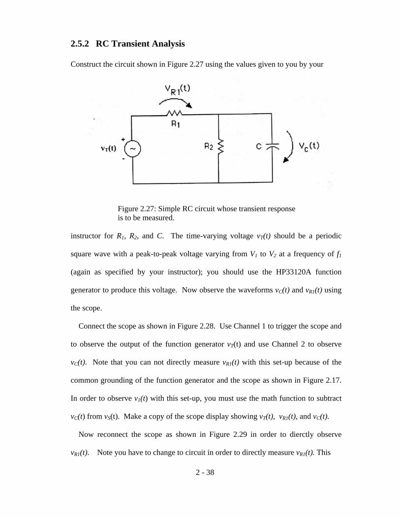
2.5.2 RC Transient Analysis Construct the circuit shown in Figure 2.27 using the values given to you by your Figure 2.27: Simple RC circuit whose transient response is to be measured. instructor for R1, R2, and C. The time-varying voltage vT(t) should be a periodic
square wave with a peak-to-peak voltage varying from V1 to V2 at a frequency of f1
(again as specified by your instructor); you should use the HP33120A function
generator to produce this voltage. Now observe the waveforms vC(t) and vR1(t) using
the scope.
Connect the scope as shown in Figure 2.28. Use Channel 1 to trigger the scope and
to observe the output of the function generator vT(t) and use Channel 2 to observe
vC(t). Note that you can not directly measure vR1(t) with this set-up because of the
common grounding of the function generator and the scope as shown in Figure 2.17.
In order to observe v1(t) with this set-up, you must use the math function to subtract
vC(t) from vS(t). Make a copy of the scope display showing vT(t), vR1(t), and vC(t).
Now reconnect the scope as shown in Figure 2.29 in order to dierctly observe
vR1(t). Note you have to change to circuit in order to directly measure vR1(t). This
2 - 38
vT(t)

is true because the signal return leads (-) of both the function generator and the scope
are connected to chassis ground as shown in Figure 2.17. Now use the math function
to observe vC(t). Make a copy of the scope display showing vT(t), vR1(t), and vC(t).
Figure 2.28: Connection used to measure the voltage across the capacitor. Figure 2.29: Connection used to measure the voltage across R1. 2 - 39
Function Gen Grounding Wire
Function Gen Grounding Wire

2.5.3 Probe Effects In this experimental section, you will investigate the effects of using two different types of scope probes. First, set the output of the HP33120A function generator to a square wave with a frequency of f2 and an amplitude of V3 peak-to-peak with the output voltage switching between V4 and V5. Use the HP5384A frequency counter to measure the frequency and the oscilloscope to measure both the peak-to-peak voltage and frequency. Now construct the circuit shown in Figure 2.30. Connect the external resistor Rex Figure 2.30: Circuit to be used for examining probe effects. to the function generator and use the 1x probe to connect it to Channel 1 input of the
scope. Note that the Function Generator negative terminal must be grounded.
Now observe vi(t) on the scope using the circuit you constructed as shown in
Figure 2.30. Make a copy of the waveform and record its period and voltage levels
plus note the ground reference. In addition, measure and record the 10-90% rise time
(tr) and the 90-10% fall time (tf). These values can be directly measured by the digital
scope.
Next, change the frequency of vsig(t) to f3 and measure and record the voltage
levels, rise time, and fall time of vi(t).
Now, change the frequency of vsig(t) back to f2, replace the 1x probe with a 10x
probe, and observe vi(t) on the scope. Make a copy of this waveform, and record
2 - 40
+
Fcn Gen Grounding to Scope
Probe33120A Function Generator

its period, voltage levels, ground reference, plus measure and record the rise and fall times. Finally, change the frequency of vsig(t) to f3 and again measure the voltage levels plus the rise and fall times of vi(t) at this frequency. 2.5.4 Electrical Relay Analysis Measurement of Relay Parameters First, use an ohmmeter to measure the coil resistance RC of your electrical relay. Record the serial number of the electrical relay and its measured coil resistance. Now, before constructing the circuit of Figure 2.31, set the output of the signal
Figure 2.31: Circuit connection that can be used to measure the relay coil inductance.
generator to a 8 volt peak-to-peak square wave switching between 0 and +8 volts with
a frequency of approximately 20 Hz. Next, leaving the setting of the function
2 - 41
33120A Function Gen.

generator fixed, construct the circuit of Figure 2.31 with RE as given by your in-
structor. Recall that Rsig = 50 Ω and use the value you measured for RC in your
computations.
If you have connected the circuit correctly and you have set the voltage levels
correctly, you should be able to hear the relay switching. If you do not hear the relay
switching, increase the peak-to-peak amplitude of the function generator output until
you do hear the relay switching. Note also how the relay is affected by the signal
frequency. If you decrease the signal frequency, the switching sound should "slow
down" and if you increase the frequency, the sound should "speed up". Eventually,
the relay will stop operating as the frequency is increased since the switch is a
mechanical device and requires a minimum amount of time to energize and de-
energize
With the frequency set to approximately 20 Hz, observe the waveforms indicated
in Figure 2.31, i.e., VT and VRE, on Channels 1 and 2, respectively, of the oscilloscope.
Be sure to include measurements of the period, amplitude, rise time, and fall time of
VRE on the scope display. Make a copy of this scope display. Now look at Channel 1,
which is the square wave output denoted by VT, and label its period and the voltage
levels. Now look at Channel 2, which is the voltage across the external resistor, and
label its period and voltage levels. Compute the coil inductance LC using the larger
of the rise time or fall time measurements.
Now disconnect the function generator output from the circuit, which can be
accomplished by unplugging the wire connecting the relay to the (+) terminal of the
function generator in Figure 2.31. Now connect the function generator output directly
2 - 42

to Channel 1 of the oscilloscope. Copy the waveform observed, making sure to note
the period and voltage levels.
Measurement of Relay Switching Times With no circuit assembled, set the output of the signal generator to a square wave
with a frequency of approximately 20 Hz. The amplitude of this square wave should
be the same as that used previously. Now construct the circuit shown in Figure 2.32
using the values given by your instructor. Observe the signal on Channel 1 of the
Figure 2.32: Circuit used to measure the relay pull-in and drop-out times, as well as to observe any contact bounce when the switch moves between the NO and NC contacts.
oscilloscope and set the scope triggering to occur at the positive going edge of this
signal. This will trigger the scope display (as well as the signal on Channel 2) when
the square wave input reaches approximately 8 volts and the relay coil is just
beginning to he energized. Adjust the time scale of the scope to show only pull-in.
2 - 43
33120A Function Gen.
Make a copy of the scope display. Now observe the signal on Channel 2 noting
the voltage levels as well as the time scale. Also, by observing this waveform,
determine and measure the relay pull-in time and label this time on your sketch.
Also, clearly identify any contact bounce present in the signal.
Now change the scope triggering to the negative going edge of Channel 1. This
will trigger the display when the square wave input returns to 0 volts and the relay
coil is just beginning to be de-energized. Adjust the time scale of the scope to show
only dropout. Make a copy of this scope display. Determine and measure the relay
dropout time by observing the waveform on Channel 2. Again, make a copy of this
waveform and label the dropout time plus identify any contact bounce in the signal.
2.5.5 RLC Transient Circuit Analysis Now, before constructing the circuit of Figure 2.33, set the output of the signal
generator to a square wave with a frequency of approximately 20 Hz. The amplitude
of the square wave should be the same as the amplitude used in the previous section.
Next, leaving the setting of the function generator fixed, construct the circuit of
Figure 2.33 with values for REC, CR, and LR as given by your instructor. Use decade
boxes for the resistance, capacitance, and inductance.
Now observe the voltage across the capacitor as indicated in Figure 2.33. If you
constructed this circuit correctly, you should see an underdamped voltage response,
i.e., the transient response should be a damped sinusoid. Make a hardcopy of this
display and label the signal period and voltage levels.
2 - 44

Figure 2.33: Circuit connection to be used for RLC transient analysis. Next, determine the frequency of the sinusoidal component of the transient
waveform. Finally, accurately measure the value of the capacitor voltage at two
positive peaks of the decaying sinusoid, that is, at two times which are an integral
number of periods apart. Make sure to record the time between these two peaks, as
well as their voltage levels.
Next, display the waveform of the current flowing in the inductor in the circuit of
Figure 2.33 by measuring the voltage across the resistor REC. First, reconnect
Channel 2 between the resistor and the inductor and use the math function to get the
voltage waveform. Adjust the voltage scales as needed to get an observable signal.
Copy this display for later comparison. Be sure the signal period and voltage levels
are shown.
Now interchange REC and CR the circuit topology in Figure 2.33 in order to
directly measure the voltage across the resistor. Note that this voltage is a direct
measure of the current through the inductor. Copy this voltage display and label it
appropriately. Also measure the values at two positive peaks separated by an integral
number of periods.
33120A Function Gen.
2 - 45

Before disassembling the circuit, compare the signal levels, shape, and period of
the two waveforms. Are they the same? If not, do you know why the math function
did not give the correct result? If not, you may wish to revisit the first configuration.
2.6 Report 2.6.1 10x Probe Adjustment 1.1 Present the hardcopies of the waveforms observed when the probe is
overcompensated and undercompensated compared to when it is critically
compensated. Why is critical compensation of the probe important?
2.6.2 RC Transient Analysis 2.6.2.1 Clearly report your analytical solutions, obtained during the advanced
preparation defined in Section 2.4 (2), for both vC (t) and vRI(t) in Figure 2.27,
assuming vs(t) as specified. Also, make a hardcopy of vC(t) and vR1(t) on the same
coordinate axis with respect to vs(t).
2.6.2.2 Present the hardcopies of the actual waveforms you observed on the
oscilloscope as a result of constructing the circuit and measuring the respective
voltages. Accurately sketch the results of your analytical solutions, presented in 2.1
above, on the hardcopies of the actual waveforms. How well do your expected
waveforms derived analytically agree with the actual measured waveforms? Give a
quantitative assessment.
2 - 46

2.6.3 Probe Effects 2.6.3.1 Using the equivalent circuit applicable to the 1x probe, show your
computations and solutions of vo(t), the signal displayed on the scope, when the input
signal has a frequency of f2. Also, show the sketch of your solution and the sketch of
the actual waveform you observed on the oscilloscope.
2.6.2.2 Using the equivalent circuit applicable to the 10x probe, Repeat 3.1 above for
the l0x probe when the input has a frequency of f3.
2.6.3.3 Construct a table that concisely summarizes your measurements. The table
should include columns for probe type, input signal frequency, scope period, peak-to-
peak voltage, tr, and tf.
2.6.3.4 Analyze the data in your table and describe the quantitative differences that
you observe. Do tr and tf change as a function of frequency or probe type? Which
probe type has the smallest tr and tf? Which type has the largest tr and tf? Is there a
trend between tr and tf, i.e., is tr always less than tf or vice versa? Finally, which
probe type has the most voltage attenuation or are they both the same? How does the
scope know that a 10x probe is being used?
2.6.3.5 Determine the total equipment capacitance of each scope probe. This can be
done by solving for the value of Ct using the equation tr = tf = 2.2τ where τ = RTCt.
Using the appropriate value for Rsig, and the average measurement of tr or tf for each
connection type, compute the capacitance for both frequencies and
2 - 47

use the average for your solution. Based upon your analysis, which probe.
has the lowest total equipment capacitance? Which one has the highest?
2.6.3.6 As indicated in Figure 2.7, the additional stray capacitance introduced by the
wires and connectors is labeled Cp. Determine a formula and solve for the value of
Cp for each probe type, i.e., 1x versus 10x, based upon the total equipment
capacitance computed in Step 3.5 above.
2.6.3.7 Based upon the information provided and the analysis performed in this experiment, when is the 10x probe not the best probe to use? 2.6.4 Electrical Relay Analysis 2.6.4.1 Indicate the value measured for the relay coil resistance and show your
computations and solution for the value of the coil inductance.
2.6.4.2 Clearly demonstrate that you understand how to analyze the circuit shown in
Figure 2.24 by determining the expressions for vE(t) and vT(t) over one period and
sketch vE(t) and vT(t) on the same coordinate axis with respect to vsig(t). For your
analysis, assume vsig(t) is a periodic square wave with a peak-to-peak voltage of 8
volts varying between 0 and +8 volts at a frequency of 20 Hz and Rsig = 50 Ω, RC =
465 Ω, RE is as given by your instructor, and LC = 1.1 Henries.
2.6.4.3 Show the copies of the actual waveforms you observed on the oscilloscope as
a result of constructing the circuit in Figure 2.31 and measuring the respective
voltages. How well do the actual waveforms agree with those expected based on the
analysis in Problem 4.2? Clearly explain the reason for any difference in the
waveforms observed for vsig(t) and vT(t).
2 - 48

2.6.4.4 For the circuit of Figure 2.32, show your sketch of the waveform observed on
the scope when the relay is energized and switches from the NC to the NO position.
Identify the relay pull-in time, period, voltage levels and any contact bounce in the
signal.
2.6.4.5 Repeat the above when the relay is de-energized and identify the relay drop-
out time, period, voltage levels and any contact bounce in the signal.
2.6.4.6 If the circuit of Figure 2.32 is modified such that the DC voltage source is V8,
R3 is replaced by R5, and R4 is replaced by R6, sketch the waveforms that would be
observed on the scope when the relay is both energized and de-energized. Explain
any differences between these waveforms and those observed in the lab using the
unmodified version of Figure 2.32.
2.6.5 RLC Transient Circuit Analysis 2.6.5.1 For the RLC circuit given in Figure 2.33, determine analytically the
expressions for the voltage across the capacitor, vCR(t), and the current in the inductor,
i(t). What are your calculated values for α, ωd, and ω0?
2.6.5.2 For the RLC circuit in Figure 2.33, show the copies of the actual waveforms
you observed for (a) the voltage across the capacitor as well as (b) the current in the
inductor. Be sure the period as well as the voltage and/or current levels are shown on
your display copies. Which of the two methods gave accurate results for
measurement of the current in the inductor?
2.6.5.3 Using the experimental data that you recorded, determine the actual values of
α and ωd. Refer to page 2-36 for equations and definitions. Be sure to show how you
2 - 49

determined these two values. What is the % error between the values of α and ωd that
you measured and the values that you calculated in step 5.1?
2.6.5.4 Draw the circuit connection that you used to directly measure the waveform
of the voltage across the resistor REC and explain how you used this voltage to
measure the current through LR. Explain why you had to use a circuit topology
different from that in Figure 2.33 to make this direct measurement.
2.6.5.5 Attached the Pspice copies make for Section 2.4 (5 and determine the values
of α and ωd. Comment on any differences you observe between the experimental
data and that from the PSpice simulation.
2.6.6 Design Problem
The problem of viewing a large, high frequency voltage (e.g., 20 kV, 1 MHz) with
the oscilloscope is not a trivial one. This problem arises in the operation of apparatus
such as radio transmitters and high frequency induction and dielectric furnaces. A
10x probe, with its maximum voltage rating of 600 V, is clearly unsuitable for this
use. An accurate reduction in the voltage of 1000x or more is necessary before
application to the scope input terminals.
A capacitive voltage divider is shown in Figure 2.34. For sinusoidal signals, this
voltage divider provides a reduction of the high voltage VH to low voltage VL in
accordance with the equation
VL/VH = Cd/(Cd + CL). (2.37)
Cd CL VLVH
Figure 2.34: Capacitive Voltage Divider
2 - 50

While a capacitive voltage divider can theoretically perform this function, lumped
capacitors have too low of a breakdown voltage for this application. Therefore, a
high voltage capacitive device must be designed to satisfy the following constraints.
(1) Clearance between high voltage parts and ground in the air must be sufficient
to avoid voltage breakdown. Four inches (10.16 cm) can be taken as adequate.
(2) For long-term reliability, clearance between high and low voltage parts in a
vacuum should exceed some minimum value, say 0.1 inch (0.254 cm).
(3) Accuracy should be little affected when using a 10x probe with the 1MegΩ,
14 pF input impedance of the scope. See Figure 2.12 on page 2 - 18.
These constraints can be satisfied by the capacitive divider structure having a
cross-section as shown in Figure 2.35. The structure is a figure of revolution made of
brass, glass, and insulating plastic. The upper part of the structure provides the input
capacitance Cd. A lumped capacitor is used for the output capacitance C. Note that
all stray capacitance due to probe and scope impedance must also be considered.
Connections to the device are made as indicated.
Figure 2.35: High voltage capacitive voltage divider device.
2 - 51
Cd
C
Vacuum
VL
VH
= Brass
= Glass
= Plastic
Output to scope using 10x probe
High Voltage Input

The design problem here is to specify the values of the lumped capacitor C and the
parallel device capacitance Cd and all dimensions of the high voltage capacitive
device so as to satisfy the above constraints, including the requirement that the
voltage attenuation factor be 1000x.
Document your design by providing the following.
6.1 Draw an overall equivalent circuit that includes (1) the equivalent circuit for the
capacitive device shown in Figure 2.35 and (2) the equivalent circuit for the
scope with a 10x probe as shown in Figure 2.12. Assuming f = 1 MHz, simplify
this overall equivalent circuit to be the circuit shown in Figure 2.34 and identify
the relationship between CL shown in Figure 2.34, C shown in Figure 2.35, and
Ct shown in Figure 2.12.
6.2 Clearly define the capacitance Cd selected for the capacitive parallel plate device
and the lumped capacitance C selected for the lumped capacitor.
6.3 Clearly define all dimensions of the capacitive parallel plate device in both
inches and cm.
6.4 State all assumptions made in arriving at your design.
6.5 Calculate the voltage seen across the lumped capacitor if the input voltage is
10 kV at 1MHz.
2.7 References
1. Nilsson, J. W., Electric Circuits, (6th ed.), Prentice Hall, Upper Saddle River, New Jersey, 2001
2. Giancoli, D. C., Physics - Principles with Applications, (5t h ed.). Prentice Hall, New Jersey, 1980
2-52