Embed Size (px)
Citation preview
Circuit Simulation of Nanotechnology Devices with Non-monotonic I-V Characteristics*
Abstract As research begins to explore potential nanotechnologies
for future post-CMOS integrated systems, modeling and simulation environments must be developed that can accommodate the corresponding problem complexity and non-traditional device characteristics. This paper describes a circuit-level simulator that can accommodate an important class of nanotechnology devices that are characterized by non-monotonic I-V characteristics. Employing adaptively controlled explicit integration method (ACES) and piecewise linear (PWL) device models, the proposed approach effectively overcomes the convergence problems and multiple equilibrium point solution problems caused by the Negative Differential Resistance (NDR) regions in such device I-V functions. Importantly, the ACES approach can address the circuit size problem when partitioning is included, and provide compatibility with simple I-V device model tables, thereby avoiding the need for analytical device models that rarely are available for nanotechnology devices. 1. Introduction
As conventional lithography-based very large scale integration (VLSI) technologies approach fundamental scaling limits, alternative technologies are being researched that may ultimately lead to a new era in nanoelectronics. Among the numerous approaches proposed for the post-CMOS era, many of the novel devices exhibit non-monotonic I-V characteristics with one or more regions of negative differential resistance. Further exploration of the utility of such devices for integrated circuit design requires a simulation environment that can be used to accurately assess the potential circuit-level performance.
The non-monotonic I-V characteristics of these devices, however, can lead to serious challenges for traditional circuit simulators such as SPICE. Oscillations may occur near the local minimum or maximum of device I-V functions in Newton-Raphson iteration, and the simulator may converge to an erroneous solution during transient simulation due to the multiple equilibrium points and ultra-fast transition time. In order to alleviate convergence problems for such circuits, heuristics such as current stepping and time-step auto reduction are proposed in [1]. Current stepping slowly steps up the peak current of each NDR devices from zero to the actual value when oscillation is detected. Time-step auto reduction reduces the time step once the device voltage is approaching its peak region. While these heuristics alleviate some of the convergence problems, their efficacy is limited by the type of device and the runtime that they can provide for very large-scale circuits.
In this paper we describe the application of piecewise linear simulation techniques and explicit integration methods for circuit level simulation of nanotechnology devices with non-monotonic I-V characteristics. With explicit integration methods, a piecewise linear circuit can be simulated through successive linear regions, which obviates the need for nonlinear iterations and thereby avoids convergence problems. Moreover, piecewise linear approximations provide efficient and adequate *This work was supported by National Science Foundation, Grant No. CCR-0205523, under ITR: Scalable Molecular Electronics.
device modeling techniques for nanotechnology circuit analysis. Model evaluation can take 50-80% of the simulation time even for traditional circuits; therefore, with nanotechnology circuit scale and analytical device models, traditional simulation methods would be impractical. The simplified piecewise linear device models, explicit integration methods, and the circuit partitioning which they can facilitate, render large-scale nanotechnology simulations practical.
A circuit consisting of devices with non-monotonic I-V characteristics can temporarily become unstable when some of the devices enter into their negative differential resistance (NDR) regions. This paper investigates the performance of different numerical integration methods and illustrates the advantage of explicit integration, specifically the ACES algorithm, for circuits with NDR devices. In order to extend the application of ACES into NDR circuit simulation, we prove that the stability of ACES for stable circuits can be maintained by simply restricting state variable derivatives from crossing their steady state derivatives in every single timestep. Utilizing this proof and the fact that the time a device stays in the NDR region is often negligible, ACES is modified such that the quiescence condition it employs for stability is not forced on every state variable when negative resistors are detected during the simulation. In such cases, only the right hand side of the circuit equations changes in every time step, and the circuit equations can be solved by a sequence of forward-backward substitution (FBS). This provides an effective way to update the circuit when devices operate in their NDR regions.
The remainder of this paper is organized as follows. Section 2 discusses the performance of different numerical integrations in piecewise linear simulation of NDR circuit. Section 3 briefly reviews the adaptively controlled explicit integration method (ACES) [2] and analyzes its stability characteristics. Section 4 and 5 follows with the implementation of ACESn, along with some results. Section 6 summarizes with our conclusions. 2. Numerical integration of NDR PWL device model circuits
Traditional circuit simulators, such as SPICE, employ implicit integration methods (such as Backward Euler and Trapezoidal) to construct companion models for energy storage elements. However, if the NDR circuit is to be simulated through successive linear regions in piecewise linear circuit simulation, implicit integration may encounter two problems.
First, due to its implicit nature, it is hard to predict the time when piecewise linear devices switch their linear regions. Iteration methods need to be applied for breakpoint prediction, which makes the simulation very costly and impractical. This problem becomes even worse when NDR devices are involved, because the time spent in the negative resistance regions is often extremely small. The same problem is encountered for PWL simulation with dominant pole methods to compute the breakpoint time [3]. However, the breakpoint prediction problem is trivial if explicit integration, such as Forward Euler, can be employed for simulation. Unlike previous integration schemes, Forward Euler provides simple and closed form trajectories. The value at the next time point can be directly extrapolated from present one, and the time to hit breakpoints
Anirudh Devgan IBM Research
Austin, TX 78758 [email protected]
Jiayong Le Dept. of ECE, CMU Pittsburgh, PA 15213
Larry Pileggi Dept. of ECE, CMU Pittsburgh, PA 15213 [email protected]
491
Permission to make digital or hard copies of all or part of this work forpersonal or classroom use is granted without fee provided that copies arenot made or distributed for profit or commercial advantage and thatcopies bear this notice and the full citation on the first page. To copyotherwise, to republish, to post on servers or to redistribute to lists,requires prior specific permission and/or a fee. ICCAD’03, November 11-13, 2003, San Jose, California, USA. Copyright 2003 ACM 1-58113-762-1/03/0011 ...$5.00.

can be explicitly calculated. Secondly, when devices have non-monotonic I-V
characteristics that can include one or more NDR regions, the circuit may temporarily become unstable. In this case, implicit integration methods can fail to capture the response of the circuit if the timestep is too large.
This instability of NDR circuits can be illustrated through
a simple FET-RTD inverter example, as shown in fig 1. The inverter works as a basic Monostable-Bistable Transition Logic Element (MOBILE). It is switched into a monostable or bistable state depending on an oscillating bias voltage (clock). During the switch process, the output voltage is influenced by the input signal. After the switch has completed, the input can no longer change the output. A detailed explanation of its operating principle can be found in [4]. Here we focus on the switching process to study the evolution of the circuit in an unstable state.
Fig 2 displays a simplified equivalent circuit for the FET-
RTD inverter where the NDR devices are substituted with their Norton equivalent models and C is the load capacitor. Assume at time t the circuit stays on one of its equilibrium points and there is a slight increase in clock signal: )()( 0 tVVtV clkclk ε∆+=
where )(tε represents a step function. Constructing and solving
the nodal equation for the output node yields:
)1()(
)(11
1210 t
eq
clk
eq
eqeqeqclk
oute
CR
V
CR
RIIVVtv α
αα−∆−
−+∆+=
The first term in the right hand side of equation (1) is the steady state response of the circuit, and α is the time constant
)2(11
21 CRCR eqeq
+=α
When the equilibrium point reaches point A in fig 1-b, the
driver RTD still works in first PDR region and the load RTD changes to NDR region (Req1>0, Req2<0). If the absolute value of Req1 is larger than Req2, α becomes negative. This sign change indicates that the circuit is physically unstable and point A is an unstable equilibrium point. In this case, the output voltage will decrease exponentially until the load RTD changes to second PDR region and the circuit reaches new equilibrium point C.
In order to correctly simulate the circuit, the simulator
must be able to capture the response of the circuit even when it is unstable so that it can find the new equilibrium point. However, the implicit integration methods in traditional circuit simulator have stability problems when the circuit is unstable. This can be best explained via the simple series RC circuit shown in fig 3.
If the resistor R in fig 3 is negative, the circuit is unstable and the step response of the circuit diverges from the steady state, as shown in fig 3-b. In other words, when t increases, the difference between the capacitor voltage and the steady state solution also increases. Conversely, the difference between the capacitor voltage and the steady state solution at time point tn+1 and tn for the series RC circuit in fig 3-a can be expressed as [5]
)3()]()([)]()([ 11RC
t
ncssncncssnc
n
etvtvtvtv∆
−
++ −=−
With a Backward Euler Approximation, the exponential
term in equation (3) is approximated by
)4(11−∆
− ∆+≈
RC
te nRC
t n
Since the resistor in fig 3-a is negative (R<0), when the timestep ∆tn>(-2RC), we will have
)5(0111
<
∆+<−−
RC
t n
When t increases, the difference between capacitor voltage and steady state solution decreases, as shown in fig 3-c. This is
Fig 2 Simplified linear equivalent circuit for FET-RTD inverter.
Vclk(t)
C
Ieq1
Vout(t) Req1
Ieq2 Req2
U(t)
-150.00
-100.00
-50.00
0.00
0 1 2 3 4 5
Fig 3 (a) A simple RC circuit and Step response of vc(t) with (b) Analytical solution, (c) Backward Euler and (d) Trapezoidal where R=-1Ω, C=1F and ∆t=2.5 > -2RC
0
0.4
0.8
1.2
1.6
2
0 5 10 15 -1.50E+04
1.50E+04
4.50E+04
7.50E+04
-3.50 0.50 4.50 8.50 12.50
vc (volts) vc (volts)
t (s)
t (s)
t (s)
vc (volts)
C
R
+_
vc(t) (a) (b)
(c) (d)
Fig 1 (a) FET-RTD Inverter and (b) load line analysis
Vin Vout
Load
Driver
Vclk
vout=low vout=high v v
v
v v
v
i
i
i
i
i
i
I: vin=high II: vin=low
vclk=low
vclk=high
A B
CD
(a) (b)
Vdd
492

incompatible with the analytical solution in fig 3-b. The damping nature of Backward Euler approximation may keep the simulated response on unstable equilibrium points in NDR circuit, which will cause false-convergence errors when the circuit has multiple equilibrium points.
For a trapezoidal approximation, the exponential term in equation (3) is approximated by
)6(11 ∆+
∆−≈∆−
RC
t
RC
te nnRC
t n
For the negative resistor (R<0), when the selected timestep ∆tn>(-2RC), we will have
)7(111 −< ∆+
∆−RC
t
RC
t nn
Though the difference between capacitor voltage value and steady state solution increases with time t, it increases in an oscillatory manner as shown in fig 3-d, which is also incompatible with the analytical solution in fig 3-b.
The aforementioned stability problems do not exist with Forward Euler integration. In Forward Euler, the exponential term in equation (3) is approximated by
)8(1RC
te nRC
t n ∆−≈∆
−
For negative resistor (R<0), (8) is always greater than one, which is compatible with the analytical solution.
In general, stability problems for different numerical
integration methods can be illustrated graphically, as shown in fig 4. The gray regions indicate damping areas for the corresponding numerical integration methods. While Forward Euler is too undamped for stable (or damped) circuits, Backward Euler is too damped for unstable (or undamped) circuits. If a circuit contains a complex pole that has a positive real part )sin(cos θθλ ir += , the transient response of the
circuit will diverge. In order to simulate this divergent response, the timesteps used in Backward Euler have to satisfy the inequality 1|1| <∆− tλ , which can also be written as
0cos2)( 2 <∆−∆ θtrtr . This expression defines the undamped
white circular region in fig 4-b, hence the largest allowable timesteps in the simulation.
The costly breakpoint prediction and stability problems render implicit integrations impractical for piecewise linear circuit simulation of NDR devices. Explicit integration, such as Forward Euler, can explicitly compute the time to each breakpoint in the piecewise linear simulation and also capture the undamped response for an unstable circuit region. This
combination of inherent features makes it very attractive for NDR circuit simulation. Furthermore, piecewise linear elements and explicit integration also allow elegant partitioning of a large circuit, which provides the necessary circuit simulation capacity. The challenge, of course, is to maintain the stability of Forward Euler when the NDR circuit operates in the stable region. Since the stability of an NDR circuit is difficult to predict, a modified Forward Euler method is required to handle both the stable and unstable circuit operation. Due to its stability characteristics, the adaptively controlled explicit integration method is a very promising candidate. 3. Adaptively controlled explicit integration
The adaptively controlled explicit integration method employs piecewise linear device models and controls time steps and derivatives of the state variables to render Forward Euler applicable for stable circuits[2]. In order to maintain stability, ACES restricts state variable derivatives from crossing their steady state. The time step for a state variable derivative to reach its steady state derivative can be calculated by
)9()(
)(tx
txxt ss
−≤∆
A state variable is defined to reach quiescence when its
derivative reaches its steady state derivative. Once the state variable reaches quiescence, it will remain there by forcing its second derivative to remain equal to zero. In other words, once a state variable reaches quiescence, the response of that variable just follows the steady state and influence of other state variables until an input or PWL region model is changed. ACES computes the response of the circuit as a transition from a condition when all state variables are nonquiescent to a condition when all state variables are quiescent. A detailed description of ACES can be found in [2].
ACES maintains stability via two strategies: (1) restricting state variable derivatives from crossing their steady state derivative in every single time step; and (2) forcing state variables to quiescence once their derivatives reach the steady state derivatives. Forcing individual state variables to quiescence increases the efficiency of stiff system (circuit with widely spread time constants) simulation. However, when the circuit includes negative resistors, the response can become unstable, and we cannot force any state variable to quiescence for a circuit with positive poles.
Since it is difficult to predict the stability of the circuit when negative resistors are involved, it would be beneficial if the stability of ACES could be assured without forcing state variable on quiescence. The rest of this section will prove that the stability of ACES for stable system can be maintained by simply restricting state variable derivatives from crossing their steady state derivatives in every time step. 3.A. Stability of modified ACES algorithm when including NDRs
With piecewise linear device models, the circuit works as a linear circuit if all devices stay in their present linear region. If capacitor voltages and inductor currents are selected as state variables as in fig 5, state equations can be constructed as
)10()(
)(
)(
)(
0)(
)(
0
0 +
−
=
tU
tIB
ti
tv
E
EG
ti
tv
L
C
L
C
T
L
C
ACES simulates the circuit in the derivative space. With the Forward Euler approximation, the derivative of state variables at time t+ t can be calculated by
tr
∆= 1
tr
∆= 1
-a aFE BE r
i i
r
(a) (b)
Fig 4 Damping Region for (a) FE (b) BE in complex pole plane
493

)11()(
)(
)(
)(
0
0
)(
)(
0
0
)(
)(
0
0
)(
)(
0
0
∆+=
∆+=∆+∆+
tv
tit
ti
tv
L
C
ti
tv
L
Ct
ti
tv
L
C
tti
ttv
L
C
L
C
L
C
L
C
L
C
L
C
Because only piecewise linear input sources are used, the steady state derivatives of the state variables are constant, therefore equation (11) can be rewritten as
)12()(
)(
)(
)(
0
0
)(
)(
0
0 ∆+
−−=
−∆+−∆+
tv
tit
iti
vtv
L
C
itti
vttv
L
C
L
C
LssL
CssC
LssL
CssC
Time steps in ACES are limited so that no state variable derivative can cross its steady state derivative in one step. Based on their initial derivatives, the state variables can be divided into two groups. The first group includes all state variables with derivatives greater than or equal to steady state derivatives at both time t and t+∆t, and the second group includes all the other state variables. Rewriting equation (12) for the first group
)13()(
)(
)(
)(
0
0
)(
)(
0
0 ∆+
−−=
−∆+−∆+
tv
tit
iti
vtv
L
C
itti
vttv
L
Ca
L
a
C
a
Lss
a
L
a
Css
a
C
a
a
a
Lss
a
L
a
Css
a
C
a
a
Since matrix C and L are diagonal, we can extract the trace of the matrices on both sides of equation (13) to yield:
( ) ( )( ) ( )
)14())()((
)()(
)()(
,,
,,,,
,,,,
+∆+
−+−=
−∆++−∆+
tvtit
itiLvtvC
ittiLvttvC
b
jL
a
iC
a
jLss
a
jL
a
j
a
icss
a
iC
a
i
a
jLss
a
jL
a
j
a
icss
a
iC
a
i
Where a
CssaC
aC vtvttv ≥∆+ )(),( and a
LssaL
aL ititti ≥∆+ )(),( .
Since the system is stable and all other state variable derivatives are less than or equal to their steady state derivatives, we have
)15(0)()(,,
<+ tvti b
jL
a
iC
It follows that (14) can be expressed as
( ) ( )( ) ( ) )16()()(
)()(0
,,,,
,,,, −+−≤
−∆++−∆+≤a
jLss
a
jL
a
j
a
icss
a
iC
a
i
a
jLss
a
jL
a
j
a
icss
a
iC
a
i
itiLvtvC
ittiLvttvC
For the second group of state variables, following similar steps we obtain
( ) ( )( ) ( )
)17(0
)()(
)()(
,,,,
,,,,
≤−∆++−∆+≤
−+− b
jLss
b
jL
b
j
b
icss
b
iC
b
i
b
jLss
b
jL
b
j
b
icss
b
iC
b
i
ittiLvttvC
itiLvtvC
Combining (16) and (17), which includes all state variables from both groups, results in:
)18()()(
)()(
,,,,
,,,,
−+−≤
−∆++−∆+
jLssjLjicssiCi
jLssjLjiCssiCi
itiLvtvC
ittiLvttvC
Setting )()( , tvCtx iCii = and )()( , tiLtx jLjj = , (18) can
be expressed as
)19()()(,, −≤−∆+ksskkssk
xtxxttx !!!!
In summary, (19) proves that the stability of ACES for a stable system can be maintained by simply restricting state variable derivatives from crossing their steady state derivative at every time step.
The stability characteristics of ACES makes it suitable for
piecewise linear simulation of NDR circuits. When all devices work in their positive differential resistance region, the ACES approach can be directly applied to calculate the transient response of the circuit. When negative resistors are detected, ACES can be used without forcing quiescence. If the circuit is unstable, eventually ACES will generate negative timesteps, thereby indicating there is no stability control and that simple Forward Euler is being applied. Since Forward Euler has no difficulty with circuits containing positive poles, the timestep is controlled by local truncation error. Because the time for which a device remains in its NDR region is very small, the degradation in efficiency caused by not placing state variables in quiescence is often negligible. 4. Implementation and Simulation Results
Based on the concept of piecewise linear simulation and explicit integration, a prototype circuit simulator, ACESn, has been implemented for the simulation of circuits containing different nanotechnology devices with non-monotonic I-V characteristics. Piecewise linear device models are constructed for nonlinear devices such as RTDs, BJTs, MOSFETs and Molecular NDR devices. Fig 6 shows the basic BJT and MOSFET models in the simulator. These device models can be made arbitrarily accurate by using more PWL segments, but at the cost of runtime efficiency.
For the DC operating point Analysis, Katzenelson
algorithm is implemented to reduce the convergence problems. Compared with Newton-Raphson algorithm, Katzenelson algorithm employs the linearity of piecewise linear device models and possesses better global convergence characteristics [6]. In transient analysis, the circuit is simulated through successive linear regions. Adaptively controlled explicit integration is used directly if all devices work in their positive differential resistance region. If negative resistors are detected,
)(tU
)(tI
Cv
Li
Source-Free memoryless
portion of the circuit
+ _ "
"
"
"
C
L
Fig 5 Linear circuit with multiple inductors and capacitors
Cutoff
Active Rev
Satrn
)10( 6−×
Cutoff
Satrn
Linear
Rev Sat
)10( 6−×
Fig 6 Piecewise linear Device Models (a) BJT and (b) MOSFET
(a) (b)
494
adaptively controlled explicit integration is applied without putting state variables on quiescence, following our proofs in Section 3.
In order to compare the simulation results, a simple analytical NDR device model from [7] is used in HSPICE and SPICE3 and the corresponding piecewise linear model is implemented in ACESn. Equation (20) gives the current-voltage relation of this model where the unknown parameters can be determined empirically for each particular NDR device of interest.
)20(
)]([tan)]([tan
43
2
1
2
1
1
kj
NT
i
VCVC
VVCVVCVCI
++−−−= −−
The first example simulated here is a modified FET-RTD
inverter circuit, as shown in fig 7-a. Its operating principle has been briefly discussed in section 2. Given the clock signal and input as shown in fig 7-b, the circuit is simulated with HSPICE, SPICE3 and ACESn. The output voltage responses are compared in fig 8.
It should be noted that HSPICE produces totally different
simulation results when the allowed maximum timestep (DELMAX) changes. When DELMAX is large, HSPICE converges to an unstable equilibrium point. SPICE3 always converges to an unstable equilibrium point for this example. ACESn successfully captures the response of the circuit, which fits quite well with the results from HSPICE using a small DELMAX (The gray line in fig 8-d). The small differences in fig 8-d can be further reduced by simply increasing the linear segments of piecewise linear devices in ACESn. But given the variations in such devices, and the errors associated with any
analytical model fitting attempts, adding more PWL regions is probably unwarranted.
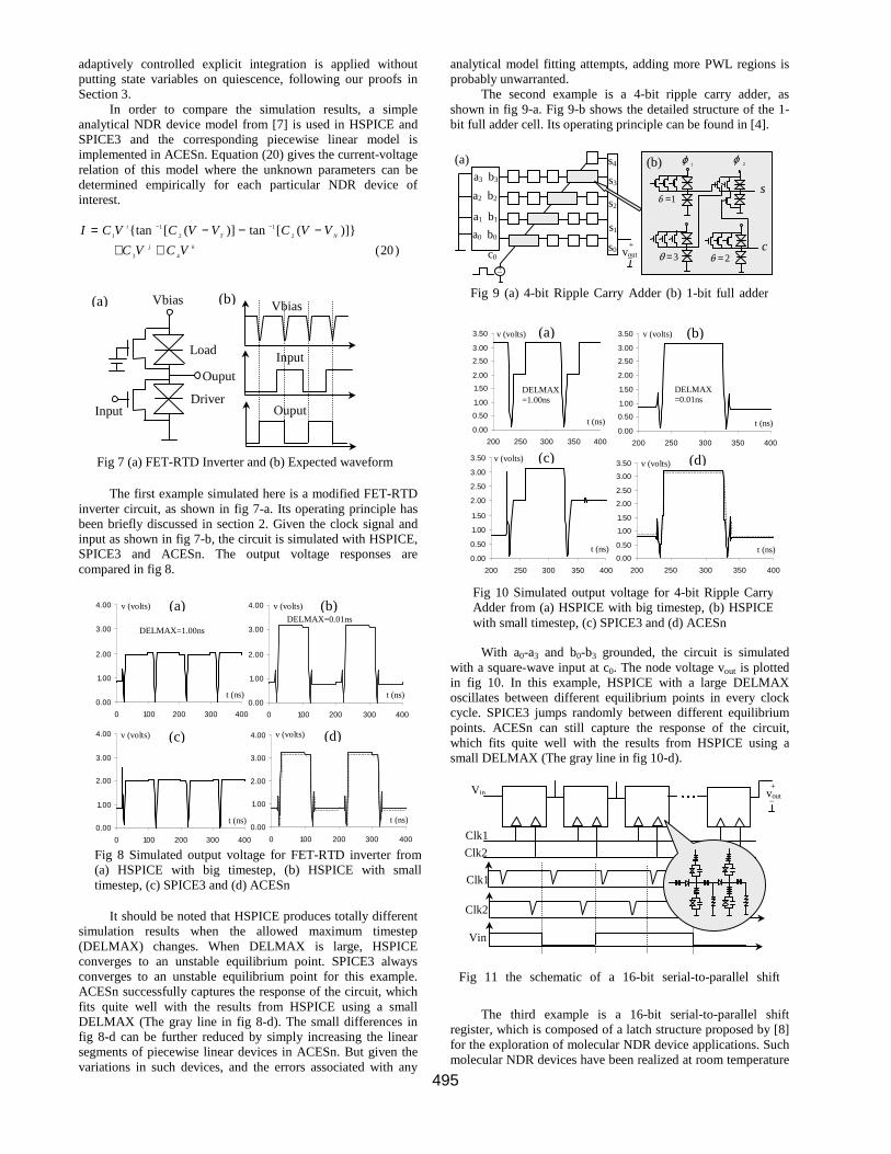
The second example is a 4-bit ripple carry adder, as shown in fig 9-a. Fig 9-b shows the detailed structure of the 1-bit full adder cell. Its operating principle can be found in [4].
With a0-a3 and b0-b3 grounded, the circuit is simulated
with a square-wave input at c0. The node voltage vout is plotted in fig 10. In this example, HSPICE with a large DELMAX oscillates between different equilibrium points in every clock cycle. SPICE3 jumps randomly between different equilibrium points. ACESn can still capture the response of the circuit, which fits quite well with the results from HSPICE using a small DELMAX (The gray line in fig 10-d).
The third example is a 16-bit serial-to-parallel shift
register, which is composed of a latch structure proposed by [8] for the exploration of molecular NDR device applications. Such molecular NDR devices have been realized at room temperature
vout
a0 b0
a1 b1
a2 b2
a3 b3
c0 s0
s1
s3
s2
s4
_
_ +
+
1=θ
2=θ3=θ
s
c
1ϕ 2ϕ
Fig 9 (a) 4-bit Ripple Carry Adder (b) 1-bit full adder cell
(a) (b)
0.00
1.00
2.00
3.00
4.00
0 100 200 300 400
0.00
1.00
2.00
3.00
4.00
0 100 200 300 400
0.00
1.00
2.00
3.00
4.00
0 100 200 300 400
0.00
1.00
2.00
3.00
4.00
0 100 200 300 400
(a) v (volts) v (volts)
v (volts) v (volts)
t (ns)
t (ns) t (ns)
t (ns)
(b)
(c) (d)
Fig 8 Simulated output voltage for FET-RTD inverter from (a) HSPICE with big timestep, (b) HSPICE with small timestep, (c) SPICE3 and (d) ACESn
DELMAX=0.01ns DELMAX=1.00ns
0.00
0.50
1.00
1.50
2.00
2.50
3.00
3.50
200 250 300 350 4000.00
0.50
1.00
1.50
2.00
2.50
3.00
3.50
200 250 300 350 400
0.00
0.50
1.00
1.50
2.00
2.50
3.00
3.50
200 250 300 350 400
0.00
0.50
1.00
1.50
2.00
2.50
3.00
3.50
200 250 300 350 400
(a) v (volts) v (volts)
v (volts) v (volts)
t (ns)
t (ns) t (ns)
t (ns)
(b)
(c) (d)
Fig 10 Simulated output voltage for 4-bit Ripple Carry Adder from (a) HSPICE with big timestep, (b) HSPICE with small timestep, (c) SPICE3 and (d) ACESn
DELMAX =0.01ns
DELMAX =1.00ns
Vin
Clk1
Clk2
Clk1
Clk2
Vin
Fig 11 the schematic of a 16-bit serial-to-parallel shift register
vout _ +
Fig 7 (a) FET-RTD Inverter and (b) Expected waveform
Ouput
Vbias
Input
Ouput Input
Vbias
Load
Driver
(a) (b)
495

[9] and are promising to be the core of the molecular latch that provides signal restoration and I/O isolation [10]. The schematic of the shift register is shown in fig 11, where each cell is composed of 4 NDR devices.
Given the waveform of two clocks (Clk1, Clk2) and input Vin as shown in fig 11, the circuit is simulated in different simulators and the output voltage vout is plotted in fig 12. In this example, we force SPICE3 to use trapezoidal integration methods. As expected from Section 2, SPICE3 shows a diverging oscillation when it reaches the unstable equilibrium points (fig 12-c). The results from ACESn and HSPICE (with small DELMAX) still fit quite well for this circuit.
5 Runtime Comparisons
Table 1 compares the runtime of ACESn and HSPICE (with small timestep) for three benchmark circuits. Although the analytical model used in HSPICE is much simpler than most analytical models for nanotechnology devices, ACESn still shows a speedup for small-scale circuits. More importantly, however, piecewise linear device models and explicit integration methods in ACESn allow elegant partitioning of large circuits, which is much more difficult in a simulation environment based on analytical models. With PWL models, large portions and/or blocks of the circuit remain latent in a linear region until an input event occurs. With analytical device models, there is no such inherent latency. It is this partitioning, which is not included for the generation of the results in Table 1, which will provide the significant speed-up and scalability for extremely large circuit sizes. Similar performance is observed for the original ACES algorithm as applied to small components without partitioning; yet it provides multiple order of magnitude runtime speedup for large CMOS circuit simulations. Table 1 Runtime comparison without partitioning in ACESn or HSPICE
Benchmark ACESn (without partitioning)
HSPICE (with small timestep)
Inverter 0.25s 32.5s 4-Adder 490s 840s Register 590s 2136s
6 Conclusions
Many novel nanoscale devices exhibit non-monotonic I-V characteristics, which can create convergence problems for
traditional circuit simulators such as SPICE. This paper explores the application of piecewise linear simulation techniques and explicit integration methods for circuit level simulation of devices with non-monotonic I-V characteristics. Employing piecewise linear device models, the proposed simulator can analyze the circuit through successive linear regions, which obviates the need for nonlinear iterations and avoids convergence problems. Using the adaptively controlled explicit integration method (ACES), the simulator can capture the response of the circuit working in both stable linear region and unstable linear region, thereby overcoming the stability problems of traditional implicit integration methods for NDR circuits.
References [1] Mayukh Bhattacharya and Pinaki Mazumder,
Augmentation of SPICE for Simulation of Circuits Containing Resonant Tunneling Diodes, IEEE Trans. on computer-aided design of integrated circuits and systems, Vol. 20, No. 1, Jan. 2001 pp 39-50
[2] Anirudh Devgan and Ronald A. Rohrer, Adaptively Controlled Explicit Simulation, IEEE Trans. on computer-aided design of integrated circuits and systems, Vol. 13, No. 6, Jun. 1994 pp 746-762
[3] Russell Kao, Piecewise linear models for switch-level simulations, Technical Report: CSL-TR-92-532, Computer Systems Laboratory, Departments of electrical engineering and computer science, Standford University, June 1992.
[4] P.Mazumder, S.Kulkarni, M.Bhattacharya, J.P.Sun, and G.I.Haddad, Digital Circuit Applications of Resonant TunnelingDevices, Proceedings of the IEEE, vol. 86, April 1998 pp 664-686
[5] Lawrence T. Pillage, Ronald A. Rohrer, Chandramouli Visweswariah, Electronic Circuit and System Simulation Methods, McGraw-Hill Professional, January 1995.
[6] Jacob Katzenelson, An algorithm for solving nonlinear resistive networks, Bell System Tech. J., Vol. 44, Oct. 1965, pp 1605-1620
[7] E.R. Brown, O.B. McMahon, L.J. Mahoney and K.M. Molvar, SPICE model of the resonant-tunneling diode, Electronics Letters, 9th, Vol. 32, No. 10 May 1996 pp 938-940
[8] Seth Copen Goldstein, Dan Rosewater, Digital Logic Using Molecular Electronics, ISSCC 2002, session 12, TD: Digital Directions, 12.5
[9] J. Chen, W. Wang, M. A. Reed, M. Rawlett, D. W. Price and J. M. Tour, Room-Temperature Negative Differential Resistance in Nanoscale Molecular Junctions, Appl. Phys. Lett. Vol. 77, 2000, pp 1224
[10] Michael Butts, Andre DeHon and Seth Copen Goldstein, Molecular Electronics: Devices, Systems and Tools for Gigagate, Gigabit Chips, ICCAD 2002, pp 433-440
0.00
0.50
1.00
1.50
2.00
2.50
3.00
3.50
1.5 1.6 1.7 1.8 1.9 2.0
0.00
0.50
1.00
1.50
2.00
2.50
3.00
3.50
1.5 1.7 1.90.00
0.50
1.00
1.50
2.00
2.50
3.00
3.50
1.5 1.7 1.9
0.00
0.50
1.00
1.50
2.00
2.50
3.00
3.50
1.5 1.6 1.7 1.8 1.9 2
(a) v (volts)
t (us)
(b)
(c) (d)
Fig 12 Simulated output voltage for the shift register from (a) HSPICE with big timestep, (b) HSPICE with small timestep, (c) SPICE3 and (d) ACESn
DELMAX=0.01ns
DELMAX=1.00ns
v (volts)
t (us)
v (volts) v (volts)
t (us) t (us)
496