Embed Size (px)
Citation preview
University of Nebraska - LincolnDigitalCommons@University of Nebraska - LincolnStudent Research Projects, Dissertations, andTheses - Chemistry Department Chemistry, Department of
4-2017
Chemical Vapor Deposition of Two-DimensionalMaterials and HeterostructuresAlex J. BosonUniversity of Nebraska-Lincoln, [email protected]
Follow this and additional works at: http://digitalcommons.unl.edu/chemistrydiss
Part of the Chemistry Commons
This Article is brought to you for free and open access by the Chemistry, Department of at DigitalCommons@University of Nebraska - Lincoln. It hasbeen accepted for inclusion in Student Research Projects, Dissertations, and Theses - Chemistry Department by an authorized administrator ofDigitalCommons@University of Nebraska - Lincoln.
Boson, Alex J., "Chemical Vapor Deposition of Two-Dimensional Materials and Heterostructures" (2017). Student Research Projects,Dissertations, and Theses - Chemistry Department. 80.http://digitalcommons.unl.edu/chemistrydiss/80
Chemical Vapor Deposition of Two-Dimensional Materials and Heterostructures
by
Alex J. Boson
A THESIS
Presented to the Faculty of
The Graduate College at the University of Nebraska
In Partial Fulfillment of Requirements
For the Degree of Master of Science
Major: Chemistry
Under the Supervision of Professor Alexander Sinitskii
Lincoln, Nebraska
April, 2017

CHEMICAL VAPOR DEPOSITION OF TWO-DIMENSIONAL MATERIALS AND
HETEROSTRUCTURES
Alex J. Boson, M.S.
University of Nebraska, 2017
Advisor: Alexander Sinitskii
A family of materials similar to graphene are transition metal dichalcogenides (TMDs)
which have emerged as an improved alternative. Importantly, each combination of TMD is
unique, possessing different properties. Chemical vapor deposition (CVD) has become a popular
method to grow TMDs at large scale and in reproducible fashion. Molybdenum disulfide (MoS2)
has been intensely studied at the monolayer due the creation of an indirect band gap but little has
been done to investigate few layered structures and as the number of layers change, so do the
properties. In this work, CVD is utilized to grow uniform bilayer and trilayer MoS2 triangular
islands and compare few layer islands to their monolayer counterpart. Another TMD, tungsten
disulfide (WS2), also has an indirect band gap at the monolayer. The combination of different
two-dimensional (2D) materials has become a new way to achieve different structures with
tunable properties. Stacking of 2D materials using van der Waals interactions has already created
a pathway to an almost limitless number of combinations. A common combination is graphene
and boron nitride because boron nitride has the same structure as graphene and creates an
insulated layer with very little charge trapping and surface defects. As a starting point for 2D
heterostructures, graphene on top of boron nitride was investigated and found to indeed reduce
charge trappings creating a Dirac point closer to zero than other dielectric substrates. With the
previous work done using CVD to grow TMDs it was also thought possible to grow MoS2 on
boron nitride to improve the quality and reduce charge trappings from the substrate. The quality
of the MoS2 became improved due to similar lattice structures leading to epitaxial growth along

the boron nitride. Finally, CVD combining the two TMDs studied above was used to create
lateral heterostructures. The combination of these two materials creates a theoretically staggered
band gap that could lead to controllable electronic or optical properties not yet explored due to
the limitations of conventional stacked heterostructures.

i
Table of Contents
Table of Figures .................................................................................................................. ii
Chapter 1: Molybdenum Disulfide ..................................................................................... 1
Background ..................................................................................................................... 1
Introduction ..................................................................................................................... 3
Experimental Procedure .................................................................................................. 6
Results and Discussion .................................................................................................. 10
Chapter 2: Tungsten Disulfide .......................................................................................... 26
Introduction ................................................................................................................... 26
Experimental Procedure ................................................................................................ 27
Results and Discussion .................................................................................................. 28
Chapter 3: Heterostructures of 2D materials .................................................................... 39
3.1 Graphene on boron nitride....................................................................................... 40
Introduction ............................................................................................................... 40
Experimental Methods ............................................................................................... 41
Results and Discussion .............................................................................................. 44
3.2 Molybdenum disulfide on boron nitride ................................................................. 54
Introduction ............................................................................................................... 54
Experimental Procedure ............................................................................................ 55
Results and Discussion .............................................................................................. 56
3.3 Molybdenum disulfide/tungsten disulfide ............................................................... 64
Introduction ............................................................................................................... 64
Experimental Procedure ............................................................................................ 65
Results and Discussion .............................................................................................. 66
Conclusion and Future Outlook ........................................................................................ 74
References ......................................................................................................................... 76

ii
Table of Figures
Figure 1 CVD growth of MoS2 islands with different thicknesses. (a) Scheme of the CVD
setup. (b) Experimental parameters for growing MoS2 with a different number of layers.
TF represents the temperature of the furnace and THP represents the temperature of the
hotplate. Arrows indicate the time when THP is increased and held constant. .....................8
Figure 2 Different shapes of MoS2 islands in the form of stars (a), hexagons (b), merging
islands (c) and uniform triangles (d). Scale bar is the same for all images. ......................12
Figure 3 Optical photograph of a Si/SiO2 substrate with monolayer (1L), bilayer (2L) and
trilayer (3L) MoS2 islands with single nucleation sites. ....................................................16
Figure 4 Characterization of MoS2 islands grown from the procedure shown in the top of
Figure 3b of trilayer synthesis. (a) Optical photograph of MoS2 crystals on Si/SiO2
containing monolayer (1L), bilayer (2L) and trilayer (3L) crystals. (b) Raman intensity
map of the area shown in the red rectangle in (a) recorded at 383 cm-1. (c) Raman spectra
of monolayer (1L) and bilayer (2L) MoS2 triangles from (b). (d) AFM image of the area
shown in the green rectangle in (a). (e) Height profiles measured along the dashed lines in
(d). ......................................................................................................................................17
Figure 5 AFM images of uniform monolayer (a), bilayer (b) and trilayer (c) MoS2
crystals. (d) Height profiles measured along the dashed lines in (a-c). .............................19
Figure 6 Comparison of optical (a) and PL (b) images of MoS2 crystals. .........................20
Figure 7 (a-c) CVD grown MoS2 triangles on Si/SiO2 recorded by (a) SEM (5 kV), (b)
SEM (1 kV), (c) optical microscopy. (d-f) Exfoliated MoS2 flakes on Si/SiO2 recorded by
(d) SEM (5 kV), (e) SEM (1 kV), (f) optical microscopy. (g) Raman spectra recorded
from the spots shown in panels (c) and (f) for different thicknesses of MoS2 crystals. ....22
iii
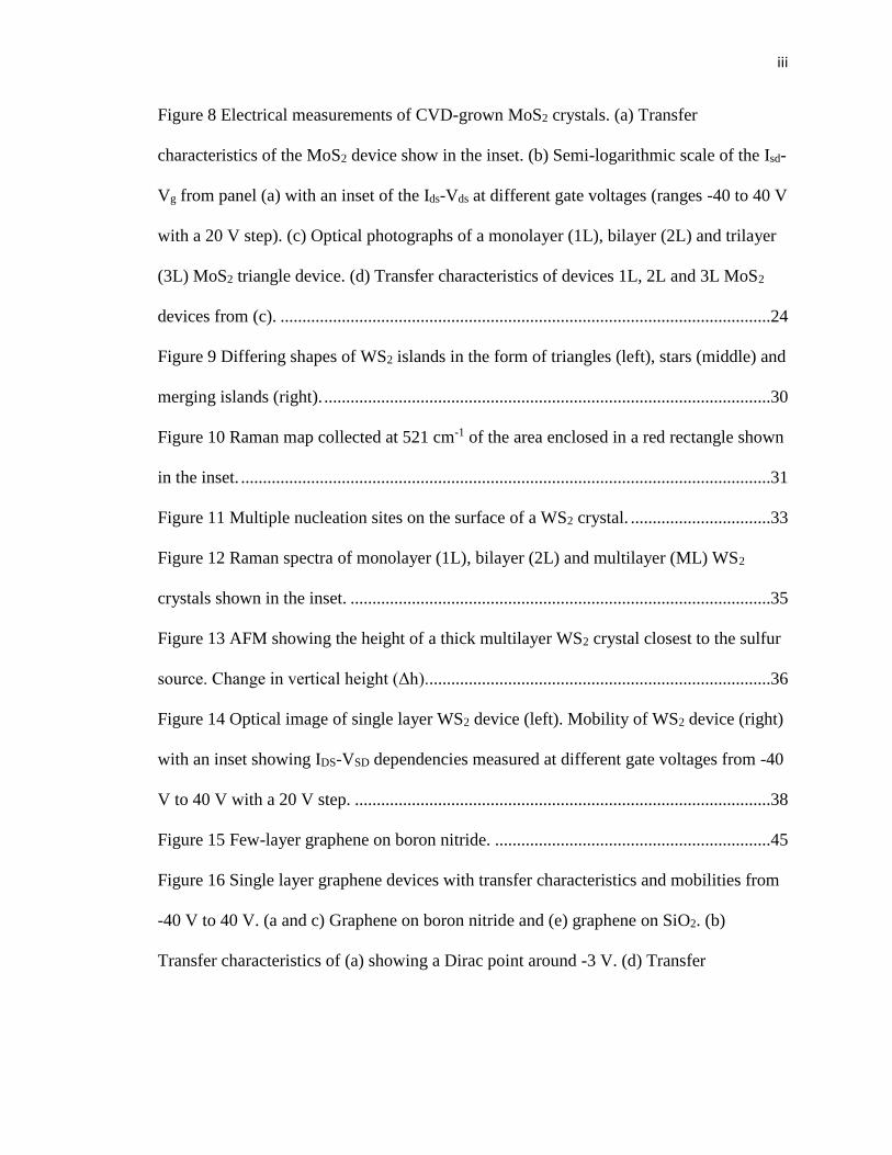
Figure 8 Electrical measurements of CVD-grown MoS2 crystals. (a) Transfer
characteristics of the MoS2 device show in the inset. (b) Semi-logarithmic scale of the Isd-
Vg from panel (a) with an inset of the Ids-Vds at different gate voltages (ranges -40 to 40 V
with a 20 V step). (c) Optical photographs of a monolayer (1L), bilayer (2L) and trilayer
(3L) MoS2 triangle device. (d) Transfer characteristics of devices 1L, 2L and 3L MoS2
devices from (c). ................................................................................................................24
Figure 9 Differing shapes of WS2 islands in the form of triangles (left), stars (middle) and
merging islands (right). ......................................................................................................30
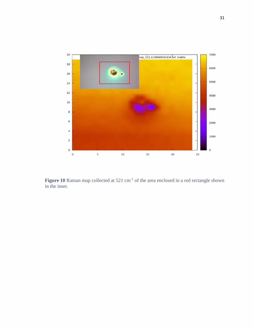
Figure 10 Raman map collected at 521 cm-1 of the area enclosed in a red rectangle shown
in the inset. .........................................................................................................................31
Figure 11 Multiple nucleation sites on the surface of a WS2 crystal. ................................33
Figure 12 Raman spectra of monolayer (1L), bilayer (2L) and multilayer (ML) WS2
crystals shown in the inset. ................................................................................................35
Figure 13 AFM showing the height of a thick multilayer WS2 crystal closest to the sulfur
source. Change in vertical height (Δh)...............................................................................36
Figure 14 Optical image of single layer WS2 device (left). Mobility of WS2 device (right)
with an inset showing IDS-VSD dependencies measured at different gate voltages from -40
V to 40 V with a 20 V step. ...............................................................................................38
Figure 15 Few-layer graphene on boron nitride. ...............................................................45
Figure 16 Single layer graphene devices with transfer characteristics and mobilities from
-40 V to 40 V. (a and c) Graphene on boron nitride and (e) graphene on SiO2. (b)
Transfer characteristics of (a) showing a Dirac point around -3 V. (d) Transfer

iv
characteristics of (b) showing a Dirac point around 3V. (f) Transfer characteristics of (e)
showing a Dirac point outside of the measured range. ......................................................46
Figure 17 Few-layer graphene device on boron nitride. (a) Optical image. (b) Transfer
characteristics of MoS2 device shown in (a). (c) ISD-VSD dependencies measured at
different gate voltages ranging from -40 V to 40 V with a 10 V step. (d) Mobility
calculation based on the transfer characteristics shown above. .........................................48
Figure 18 (a) Few-layer graphene on both boron nitride and PZT. (b) Enlarged area of (a)
showing the difference between the graphene on boron nitride/PZT (left portion) and just
PZT (right portion). Device fabricated of the graphene on (c) boron nitride/PZT. and (d)
PZT. ...................................................................................................................................50
Figure 19 Transfer characteristics of Gr-PZT (left) and Gr-BN-PZT (right), where Gr
stands for graphene and BN stands for boron nitride. .......................................................51
Figure 20 A second layer of boron nitride placed on top of the graphene previously laid
upon a boron nitride flake with a top-gate FET (top). Transfer characteristics of the
device shown above at different voltages ranging from -1 V to 1 V through -5 V to 5 V
(bottom)..............................................................................................................................53
Figure 21 Optical image demonstrating MoS2 nucleation being favored at the edges of
boron nitride (left). SEM image of the optical image from the left panel of MoS2 growth
around and on top of boron nitride (right). ........................................................................58
Figure 22 SEM image demonstrating the alignment of MoS2 triangles compared to the
edges of boron nitride. .......................................................................................................60
Figure 23 Optical image of very thin boron nitride flake containing multiple thicknesses
of few layers prior to MoS2 growth (left). SEM image of MoS2 grown on/around the

v
boron nitride flake with no epitaxial alignment or very little triangular growth seen
(right). ................................................................................................................................61
Figure 24 SEM image of boron nitride with thickness ranging from double layer (red) to
greater than 100 layers (green), the thinnest parts showing no epitaxy and the thicker
areas with good alignment can be seen in Figure 22. ........................................................62
Figure 25 AFM confirming single layer MoS2 triangles are grown in the thicker region of
boron nitride. Change in vertical height (Δh). ...................................................................63
Figure 26 Raman of the optical image from the inset. The black dot corresponds to the
Raman shown in black confirming growth of WS2.The red dot corresponds to the Raman
shown in red confirming growth of MoS2. ........................................................................68
Figure 27 Optical image of a heterostrucutre (left). Raman maps taken of the sample from
the left panel. Raman map of MoS2 recorded at 403 cm-1 (middle) and Raman map of
WS2 recorded at 351 cm-1 (right). ......................................................................................69
Figure 28 AFM from the center region to the outer region similar to the flake shown in
Figure 25 showing no discernable change in the height between the two structures. .......70
Figure 29 PL map of the same sample shown in Figure 27. ..............................................72
Figure 30 Primary attempt at measuring electronic properties of an in-plane MoS2/WS2
heterostructure device. .......................................................................................................73

1
CHAPTER 1: MOLYBDENUM DISULFIDE
Background
The discovery of graphene, a sp2 hybridized planar sheet of carbon atoms, has
caused an eruption of new two dimensional materials to be studied. Graphene’s unique
properties, such as its strength,1 flexibility,1,2 high charge carrier mobility,3–5 high
surface-to-volume ratio6 and transparency,7,8 are different from the properties of its bulk
counterpart, i.e. graphite, and highly desired for a number of applications, including RF
transistors, gas sensors and transparent conductors among others.
The major problem with graphene for electronic applications is its lack of an
energy band gap. Band gap refers to the energy required to excite an electron from the
valence band to the conduction band so that it may conduct electricity. Graphene’s band
structure is unique because it consists of two cones touching at the tips, or Dirac points.9
In these cones, the two-dimensional energy dispersion relation is linear making electrons
and holes degenerate.10,11 Since graphene does not have a band gap, it acts like a
semimetal, giving it a very poor on/off ratio in field-effect transistors (FETs) of up to ~55.
Its shortcomings are what have led to the interest in alternative two-dimensional materials
with semiconductor properties.
Other materials in the graphene family include hexagonal boron nitride (often
referred to as “white graphene”),12 boron carbon nitride (BCN),13 fluorographene14 and
graphene oxide7 among others. “White graphene” is an insulating material, so it cannot
be used as a device channel, although it finds applications as a substrate dielectric for
2
improved graphene based devices.12 The other materials, such as fluorographene,
mentioned to be in the same family of graphene have proven thus far to have very poor
electronic qualities14 or are non-stoichiometric making them difficult to control.15,16 A
second set of materials that exist as two-dimensional materials are oxides, which are
more stable in air than many monolayer materials, but also more susceptible to changes
when in contact with water and protic solvents. This poses many problems for the entire
family of oxides outside of simply stability, their use in reactions would be limited as
well as characterization and fabrication techniques diminished.17
A very most promising group of two-dimensional materials, most of which
actually have semiconductor properties, are transition metal dichalcogenides (TMDs), of
which the most prominently studied two-dimensional material up to this point besides
graphene has been molybdenum disulfide (MoS2).17–21 TMDs have a transition metal
(e.g., Mo, W, Nb, Ta) “sandwiched” between two chalcogen layers (e.g., S, Se, Te).
Graphene and TMDs share many similarities characterized by noncovalent bonding
between layers and strong in-plane covalent bonding.17
Majority of studies use MoX2 and WX2 because they have been shown to be
semiconducting, whereas NbX2 and TaX2 are metallic making them less versatile for
transistor applications.22–25 Regardless of bulk or monolayer, the band gaps of many
TMDs are comparable to or exceed that of the 1.1 eV of silicon.26 One of the most
important properties of MoS2 is that as a crystal it has an indirect band gap of ~1.3 eV,
and as the number of layers decreases to a monolayer, it becomes a semiconductor with a
direct band gap of ~1.9 eV.27 The reason for an increase in the band gap is generally due
to confinement of carriers in the out-of-plane direction inducing a gradual increase in the
3
band gap with decreasing thickness.28 Since the monolayer MoS2 has a direct band gap, it
is promising for the electronics industry, which is driven by scaling down the size of
transistors and is reaching the limit for current silicon-based transistors.26
Current field-effect transistors (FETs) use a semiconducting channel region
connected to source and drain electrodes that are made of an inert conducting material,
i.e. gold, while an insulating layer, such as silicon oxide (SiO2), is used as a gate
dielectric.29 The current that flows between the source and drain electrodes through the
semiconducting channel can be modulated by the voltage applied to the gate electrode.
There are many different factors that can affect the electronic characteristics of a device,
specifically the mobility of carriers is affected by different types of scattering, such as
Coulombic impurities,30 surface interfacial phonons and roughness scattering.4,12,31
Minimizing these scattering effects can lead to improved mobilities in FETs and bring the
characteristics of current devices closer to theoretical calculations. This study includes
results of FET measurements of TMD materials, as well as describes efforts on
minimization of scattering effects in TMDs by growing them on atomically flat
crystalline hexagonal boron nitride substrates.
Introduction
As the most studied TMDs, MoS2 has been found to have a large number of
applications such as its use in field-effect transistors (FETs) due to its high on-off
ratios,32–34 gas sensors with its n-type semiconducting nature,35 photodetectors,36
optoelectronics such as ferroelectric memories,37 and energy storage in batteries.38 The
reason MoS2 has been favored over materials utilizing tungsten or selenium is because of
the larger availability of molybdenite crystals, and their higher chemical stability

4
compared to most other TMDs. After becoming “the standard” for TMD, MoS2 growth
has been studied in a multitude of ways.
Because of the weaker out-of-plane bonding, it very easy to mechanically
exfoliate single to few layers of these materials from the bulk crystals. Mechanical
exfoliation is simply the peeling away of a material layer by layer, which in the case of
graphene and TMDs is the disruption of weak van der Waals attractions. The most
common way to exfoliate these materials is using adhesive tape to overcome the van der
Waals forces holding the layers together.39 This top-down approach of preparing these
single to few layered materials has many problems which are difficult to overcome, such
as reproducibility, uniformity and the size of the flakes created. Alternative exfoliation
techniques of TMDs and other two-dimensional materials are not limited to the
mechanical exfoliation, liquid-phase exfoliations have also been performed.40 In one
method, it was found that the flakes exfoliated in this manner were monolayer with sizes
of <1 µm, and since lithium is used, it increases the cost and risk of flammability. A
second liquid-phase technique, involves the use of sonication in different solvents such as
isopropanol, dimethylformamide, dimethyl sulfoxide, and cyclohexanone.41 and
surfactant solutions, e.g. sodium cholate, taurodeoxycholate, lithium dodecyl sulfate, and
others.42 These methods are much safer and cost effective than using lithium intercalation
but give low yield of monolayer flakes.
Despite the problems, mechanical exfoliation of graphene using tape has shown
the best results in terms of physical and electrical properties.4 Likewise, much research
has been done on exfoliated flakes of MoS2, but a different approach to making these
materials is bottom-up synthesis where the materials are synthesized at the atomic level.

5
Chemical vapor deposition (CVD) has allowed for the synthesis of large-scale, large-area
growth of single layer MoS2 not reproducible via exfoliation, although the CVD-grown
MoS2 is still routinely compared to the top-down exfoliated samples.34 The most common
CVD techniques of producing MoS2 rely on sulfur powder and a separate source of
molybdenum, such as MoO3,43–48 MoCl5,
49 or metallic molybdenum.50 Other CVD
techniques that have been done are the vapor phase transport and recrystallization of
MoS2,51 thermal decomposition of (NH4)2MoS4,
52 and metal-organic CVD.53
The growth of MoS2 is predominately triangular with a single nucleation point
leading to monolayer islands that grow outward, potentially merging with nearby islands
to form lager continuous monolayers. Although the grain boundaries between domains of
merging islands do not affect the electronic properties as seen in the individual triangles
of MoS2,47 they are still most often used in research because their shape can be correlated
with the MoS2 crystallographic orientations. There have been other growth types
reported, i.e. star shaped54 and hexagonal,48,55 that form due to differences in procedure
that lead to alteration of growth kinetics or the amount of chalcogen used.
While most studies pertain to the monolayer MoS2, very little work has been done
on multilayer MoS2, especially uniform bilayer and trilayer MoS2 triangular islands.
Some unique properties that multilayer two-dimensional materials possess over their
monolayer counterparts originate from different van der Waals interactions between the
layers. The different ways the layers of MoS2 can grow on top of one another has been
studied extensively to differentiate between stacking order; a 0o twist angle between two
layers (AB stacking) and a 60o twist angle (AA’ stacking) being the major
conformations.56 The stacking configuration can play an important role in the size of the
6
band gap, changing with the twist angle57. The van der Waals interactions between layers
are what eliminate the direct band gap of MoS2 and create an indirect one, which explains
the absence of photoluminescence in few-layer MoS2 compared to monolayer crystals.21
In this chapter, a CVD procedure is established that yields continuous bilayer and
trilayer MoS2 islands. Characterization via Raman spectroscopy, atomic force
microscopy (AFM) and photoluminescence (PL) microscopy provides data that conforms
to what has already been established for single to multilayer MoS2. Due to the difference
in the band gap type (direct versus indirect) as seen by the stark contrast in PL, it was
determined that monolayers of MoS2 could also be differentiated from few-layers with
scanning electron microscopy (SEM) at very low accelerating voltages. After confirming
the results, electrical measurements were also performed on monolayer and few-layer
MoS2 flakes.
Experimental Procedure
MoS2 crystals were grown on p-doped silicon substrates covered with 300 nm-
thick silicon oxide (SiO2). Substrates were cleaned for 10 minutes in acetone, 10 minutes
in deionized water, and 10 minutes in 2-propanol before being put into a UV ozone
cleaner, ProCleanerTM Plus system for 30 minutes. Once the substrates are clean, 0.5-1
mg of molybdenum (VI) oxide (99.95%, Alfa Aesar) was placed into the center of a clean
40 mm quartz boat. One substrate (1 x 0.25 cm2) was placed with the SiO2 layer facing
away from the MoO3 (indicated face-up) directly over the center of the MoO3 and the
second substrate (~2 x 2 cm2) was placed with the SiO2 layer facing toward the MoO3
(face-down) with one edge aligned over center of the MoO3. The quartz boat was then
loaded into a 2-inch quartz tube in a Lindberg Blue M tube furnace. A second quartz boat

7
was prepared with 50 mg of sulfur (99.999%, Acros Organics) and placed ~35 cm
upstream of the MoO3, over the center of a hotplate. The CVD setup can be seen in
Figure 1a.

8
Figure 1 CVD growth of MoS2 islands with different thicknesses. (a) Scheme of the
CVD setup. (b) Experimental parameters for growing MoS2 with a different number of
layers. TF represents the temperature of the furnace and THP represents the temperature of
the hotplate. Arrows indicate the time when THP is increased and held constant.
9
The system was flushed with argon three times and the growth procedure was
performed at atmospheric pressure with 100 sccm of argon flowing throughout the
growth procedure. The CVD procedure starts as the temperature goes up to 300 ºC over
30 minutes, remains at 300 ºC for 30 minutes, then climbs to 550 ºC over 30 minutes to
remove any water or surface contaminates that remained after cleaning. After reaching
550 ºC the temperature is further increased to 800 ºC over 10 minutes, held at 800 ºC for
10 minutes, and cooled slowly until 380 ºC before opening the furnace to cool back to
room temperature.
To produce single layer MoS2 the above procedure was followed by increasing
the temperature of the hot plate, THP, to 250 ºC at 5 minutes before the temperature of the
furnace, TF, reaches 800 ºC. Monolayer MoS2 triangles were grown similarly to
previously reported studies.58 In order to produce multilayer MoS2 the same procedure as
above was followed except with a change to the rate of sulfur evaporation. By increasing
the THP to 275 ºC when TF reaches 800 ºC a bilayer of MoS2 was produced. If THP is
increased again to 300 ºC after 5 minutes at 800 ºC, an allotment of trilayer MoS2 islands
form.
Raman spectroscopy was performed using a Thermo Scientific DXR Raman
microscope with a 532 nm laser. SEM images were taken using a Hitachi S4700 field
emission scanning electron microscope in secondary electron detection mode at the
accelerating voltage of 5 kV. Atomic force microscopy (AFM) images were recorded
using a Bruker Dimension Icon Atomic Force Microscope equipped with ScanAsyst.
Photoluminescence (PL) microscopy was performed using a Nikon Eclipse Ti-E inverted

10
microscope with a Cy5 filter cube with an excitation cut-off at ~652 nm and an emission
cut-off at ~671 nm.
For device fabrication, a Zeiss Supra 40 field-emission scanning electron
microscope and a Raith pattern generator were used for electron beam lithography (EBL)
and an AJA electron beam evaporator was used for electron beam evaporation (EBE), the
detailed procedure for the device fabrication can be found elsewhere.59 Electrical
measurements of the devices mentioned above were performed using a Lake Shore TTPX
cryogenic probe station at a base pressure of ~2 x 10⁻⁶ Torr. The device electrodes were
connected to an Agilent 4155C semiconductor parameter analyzer that was linked to a
computer through 82357B USB/GPIB interface and controlled using a National
Instruments LabView code.
Results and Discussion
Earlier work done in this field had yielded a method of getting single layer flakes
of MoS2 but not quite as consistently in shape or quality as was desired. The process of
growing consistent single layer MoS2 triangular islands was adapted from previous work
by tweaking growth points and additional parameters, see Experimental section for
optimized growth conditions currently used. By adjusting the conditions, more uniform
triangular islands of MoS2 could be seen all around the substrate rather than a mix of
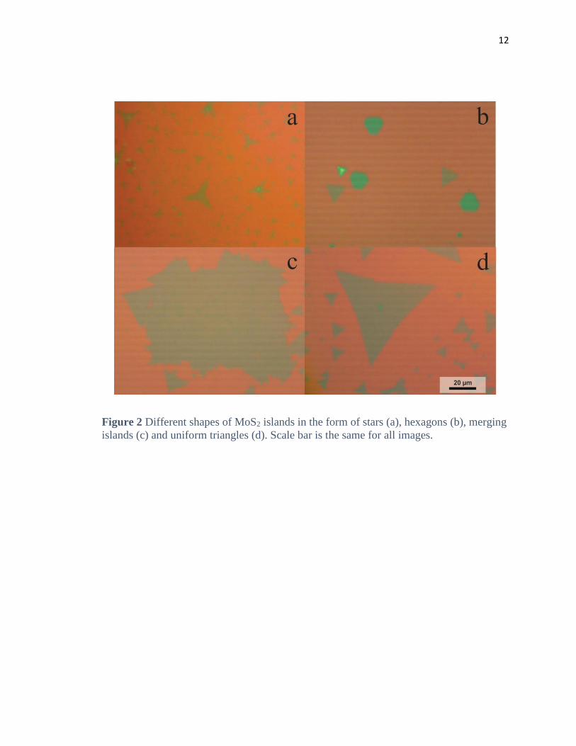
triangles, stars, hexagons, and merging islands, Figure 2.
Star-shaped MoS2 tends to occur when the cooling time was fast, not allowing the
sulfur enough time to reach the MoO3 and to fully react. More complete triangular islands
were grown by turning the hotplate on earlier in the process rather than after maximum
temperature was reached or once cooling began rather than the star shapes originally

11
seen. Formation of hexagons and merging islands of MoS2 was reduced by limiting the
amount of MoO3 allowed to reach the second/larger substrate. To limit the overall
nucleation that can occur and restrict the number of merging islands, the amount of MoO3
used was reduced and a smaller substrate was placed between the desired substrate and
molybdenum source.
12
Figure 2 Different shapes of MoS2 islands in the form of stars (a), hexagons (b), merging
islands (c) and uniform triangles (d). Scale bar is the same for all images.

13
After consistent growth of uniform MoS2 triangular islands the next task was to
try and grow uniform layered triangles. As could sometimes be seen in the adjusted
growth procedure, some of the triangles formed had a very clear nucleation site visible in
the center of the triangle and even some with growth occurring off that nucleation site
presenting the beginning of a second layer Figure 2d. The assembly of a second layer on
top of a single layer is something that has already been studied in detail but almost no
work has been done on a uniform few layer islands of MoS2.
The areas that seemed to have more appearances of a bilayer on the substrate were
closer to the center of the boat where the oxide is originally placed, indicating that the
area nearer the sulfur may grow taller structures. A possible explanation for these thicker
islands was due to a faster rate of sulfurization. Unfortunately, it was not the case for
when the rate of sulfur was simply increased by raising the temperature of the hotplate
immediately upon reaching growth temperatures, no thicker uniform islands were seen.
An array of different temperatures was tested, every 5 ºC upward of 250 ºC all the way to
300 ºC, but nothing different grew than at the initial 250 ºC introduction point. In fact,
even fewer structures were seen overall than before and even less uniform in shape than
the previously shown. This was most likely due to the sulfur simply flowing past the
molybdenum faster than it was depositing on the substrate creating less opportunity for
growth to occur.
As a result of less growth with an increase in temperature, the idea that the
monolayer triangles needed time to properly form before the second layer formation can
begin emerged. To allow time for a monolayer to grow, the procedure for single layer
triangular islands was used and after 5 minutes, the temperature of the hot plate was

14
increased in three separate experiments first by 10 ºC, then 20 ºC and 30 ºC, respectively,
to see if growth of a second layer would form if the nucleation site atop the monolayer
was given time to form first. Incomplete growth was seen at 260 ºC leaving more
monolayer islands at the early stages of the second layer formation. More uniform bilayer
triangles were then seen at the 20 ºC and 30 ºC increases but at 280 ºC the triangles
appeared to be smaller than the complete bilayer found at 270 ºC. It was decided that the
rate of sulfur deposition was too fast, and the second layer was reaching the edge of the
still growing single layer inhibiting the growth. Without enough energy in the system, the
second layer of MoS2 will halt the first layer from continuing to expand outward because
the second layer will grow at a faster rate than the first due to more sulfur being deposited
faster at the nucleation site. As such, the sulfur flow rate at 280 ºC was limiting the
growth of the triangles, and 275 ºC was used to encompass both better size and
uniformity.
At the creation of a uniform bilayer MoS2 triangle, the idea to expand this to a
third layer by the same process was decided. After allowing time for the bilayer to begin
forming, the temperature was increased again by 25 ºC. A sample produced by this final
approach is shown in Figure 3 with labelled monolayer, bilayer and trilayer MoS2 crystals
(the same area of the same without labels is shown in Figure 4a). It is easy to distinguish
monolayer MoS2 just by the optical contrast on 300 nm-thick SiO2 under an optical
microscope, while the bilayer and trilayer islands can be differentiated by color. The
thickness of the crystals was also verified by Raman spectroscopy, AFM and PL
microscopy. All of the MoS2 crystals in Figure 3 are labelled to indicate the number of
layers; of the 123 islands shown. Only 19 are monolayer (15.5%), 72 are bilayer (58.5%)
15
and 32 are trilayer (26%). For the growth procedure of trilayer MoS2 as depicted in
Figure 1, the sample shows an area of 84.5% multilayer growth but with other areas of
varied growth scattered throughout the substrate, but several comparable areas were
commonly seen. This makes for very simple identification of large (>10 µm) uniform
bilayer and trilayer MoS2 crystals.
Characterization of these flakes was done with several different techniques.
Raman spectroscopy can differentiate between monolayer, bilayer and trilayer MoS2
crystals based on spectral positions of the 𝐸2𝑔1 (~383 cm-1) and A1g (~405 cm-1)
modes.60,61 As the number of layers in a MoS2 crystal increases, the separation between
the 𝐸2𝑔1 peak and A1g peak grows from ~19 cm-1 (monolayer) to ~25 cm-1 (bulk)60. Figure
4b shows a Raman intensity map of the area outlined by the red square in Figure 4a at
382 cm-1 demonstrating that bilayer MoS2 crystals give a higher Raman intensity than
that of monolayer crystals. Figure 4c shows a representative Raman spectra recorded for
both the monolayer and bilayer MoS2 triangles shown above.

16
Figure 3 Optical photograph of a Si/SiO2 substrate with monolayer (1L), bilayer (2L) and
trilayer (3L) MoS2 islands with single nucleation sites.

17
Figure 4 Characterization of MoS2 islands grown from the procedure shown in the top of
Figure 3b of trilayer synthesis. (a) Optical photograph of MoS2 crystals on Si/SiO2
containing monolayer (1L), bilayer (2L) and trilayer (3L) crystals. (b) Raman intensity
map of the area shown in the red rectangle in (a) recorded at 383 cm-1. (c) Raman spectra
of monolayer (1L) and bilayer (2L) MoS2 triangles from (b). (d) AFM image of the area
shown in the green rectangle in (a). (e) Height profiles measured along the dashed lines in
(d).
18
Another technique used to measure thickness of MoS2 crystals is AFM. The AFM
shown in Figure 4d is of the area outlined by the green square in Figure 4a. According to
the height profiles given by the dashed lines intersecting the triangles shown in Figure 4d
the area contains monolayer (1L), bilayer (2L) and trilayer (3L) MoS2 crystals. The
monolayer measured in Figure 4e gives a thickness of ~0.7 nm which is consistent with
previously reported literature of other CVD-grown MoS2 triangles44. If the heights add up
as expected, then it follows that the bilayer should have a thickness of ~1.3 and trilayer a
thickness of ~2.0, which in fact they do. While the trilayer in this sample is actually
terraced, not uniform, it gave a good representation of how all three layers can grow in
the same area. A uniform trilayer crystal that could be observed in many places on the
flake is show in Figure 5c. Figure 5a-c shows how similar the three different layers of
MoS2 triangles may appear, only differing in height (Figure 5d).
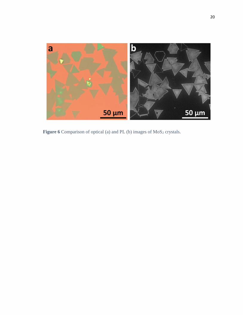
Since bulk MoS2 all the way down to bilayer has an indirect band gap while
monolayer has a direct band gap, the difference between monolayer and multilayer can be
distinguished by PL microscopy. Figure 6 shows images of optical and PL microscopy of
a sample grown with bilayer conditions previously mentioned with a maximum THP of
275 ºC. Although monolayer MoS2 crystals show a bright emission in Figure 6b,
multilayer crystals remain dark, except for the edges. The reason some of the monolayer
crystals do not look as uniform has been reported to be the result of sulfur deficiency.43
PL shows a more detailed image of monolayer MoS2 flakes. However, PL is impractical
on samples with flakes thicker than one layer, or to differentiate between thicknesses
beyond one to two layers.

19
Figure 5 AFM images of uniform monolayer (a), bilayer (b) and trilayer (c) MoS2
crystals. (d) Height profiles measured along the dashed lines in (a-c).
20
Figure 6 Comparison of optical (a) and PL (b) images of MoS2 crystals.
21
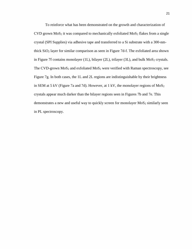
To reinforce what has been demonstrated on the growth and characterization of
CVD grown MoS2 it was compared to mechanically exfoliated MoS2 flakes from a single
crystal (SPI Supplies) via adhesive tape and transferred to a Si substrate with a 300-nm-
thick SiO2 layer for similar comparison as seen in Figure 7d-f. The exfoliated area shown
in Figure 7f contains monolayer (1L), bilayer (2L), trilayer (3L), and bulk MoS2 crystals.
The CVD-grown MoS2 and exfoliated MoS2 were verified with Raman spectroscopy, see
Figure 7g. In both cases, the 1L and 2L regions are indistinguishable by their brightness
in SEM at 5 kV (Figure 7a and 7d). However, at 1 kV, the monolayer regions of MoS2
crystals appear much darker than the bilayer regions seen in Figures 7b and 7e. This
demonstrates a new and useful way to quickly screen for monolayer MoS2 similarly seen
in PL spectroscopy.

22
Figure 7 (a-c) CVD grown MoS2 triangles on Si/SiO2 recorded by (a) SEM (5 kV), (b)
SEM (1 kV), (c) optical microscopy. (d-f) Exfoliated MoS2 flakes on Si/SiO2 recorded by
(d) SEM (5 kV), (e) SEM (1 kV), (f) optical microscopy. (g) Raman spectra recorded
from the spots shown in panels (c) and (f) for different thicknesses of MoS2 crystals.

23
Finally, the electronic properties of the CVD-grown MoS2 crystals on Si/SiO2
substrates were assessed. Ti/Au (1 nm/20 nm) electrodes were fabricated onto MoS2
crystals. A FET shown in Figure 8a depicts a MoS2 channel bridging two Ti/Au source
(S) and drain (D) electrodes on Si/SiO2. The silicon was used as a back gate (G) and is
heavily doped toward the p-type silicon. The devices were allowed two days of
evacuation in order to minimize the effect of surface adsorbates62.
Figure 8a demonstrates the properties of a monolayer MoS2 FET with a n-type
source-drain current (ISD)-gate voltage (VG) dependence with electron mobilities reaching
2.5 cm2 V-1 s-1. The source-drain current (ISD)-source-drain voltage (VSD) dependences
are Ohmic at all gate voltages (Figure 8b insert). A semi-logarithmic scale of the same n-
type ISD-VG dependence shows the device has an ON/OFF ratio of ~105, Figure 8b. In
total, 15 devices based on monolayer MoS2 triangles were measured and show consistent
electron mobilities of 2.7 ± 0.9 cm2 V-1 s-1 with ON/OFF ratios ranging from 103 to 105.
Devices made of bilayer and trilayer MoS2 crystals exhibited similar properties.
A comparison of the conductivity between the different layers of devices optically
shown in Figure 8c can be seen below in Figure 8d. From the graph, it can be seen, that
as the number of layers increases so does the conductivity. The electron mobilities reach
3.1 cm2 V-1 s-1 for 1L MoS2, 4.5 cm2 V-1 s-1 for 2L and 9.5 cm2 V-1 s-1 for 3L. Overall,
eight bilayer MoS2 FETs were measured with an average mobility of 4.7 ± 1.6 cm2 V-1 s-1
and seven trilayer MoS2 FETs with an average mobility of 7.3 ± 2.3 cm2 V-1 s-1. The
ON/OFF ratios for each multilayer measured had the same range as monolayer, 103 to
105.
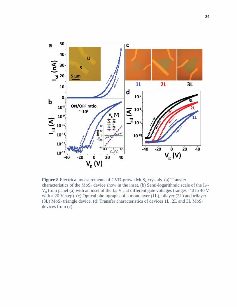
24
Figure 8 Electrical measurements of CVD-grown MoS2 crystals. (a) Transfer
characteristics of the MoS2 device show in the inset. (b) Semi-logarithmic scale of the Isd-
Vg from panel (a) with an inset of the Ids-Vds at different gate voltages (ranges -40 to 40 V
with a 20 V step). (c) Optical photographs of a monolayer (1L), bilayer (2L) and trilayer
(3L) MoS2 triangle device. (d) Transfer characteristics of devices 1L, 2L and 3L MoS2
devices from (c).

25
In summary, the new growth procedure for MoS2 crystals grown in CVD from
MoO3 and sulfur yield prominently bilayer and trilayer MoS2 islands. Additional layers
can only form after the initial nucleation and growth of the monolayer has occurred. This
method allows for uniform bilayer and trilayer islands rather than the more often reported
terraced structures,56,57 although some terraced growth does still occur. It was revealed
that along with traditional forms of characterization for MoS2 (Raman spectroscopy,
AFM and PL microscopy), SEM can also be used to distinguish between monolayer and
few-layered MoS2 flakes at low accelerating voltages. Lastly it was demonstrated that
electron mobility increases with increasing layer counts.

26
CHPATER 2: TUNGSTEN DISULFIDE
Introduction
Another well-studied TMD that works in comparison to molybdenum disulfide
(MoS2) is tungsten disulfide (WS2). While the valence band energy of WS2 is higher than
that of MoS2, so is the conduction band energy. The result gives a comparable band gap
to MoS2 at ~1.3 eV as bulk crystal and ~2.1 eV as a monolayer25. However, with a
slightly larger splitting, it should have a slightly larger band gap than MoS2 making it an
even better material for electronic devices. Another benefit of WS2 is that the higher PL
emission efficiency28 could potentially lead to unique heterostructures with adaptive
optical and electrical functions.19,63
As was shown with mechanical exfoliation of graphene and MoS2, mechanically
exfoliated WS2 has also shown greater efficiency compared to its bottom-up grown
counterpart. Different CVD approaches to growing WS2 are also similar to those of
MoS2, and include the reaction of tungsten (VI) oxide (WO3) with sulfur,64 sulfurization
of thermally deposited tungsten oxide films,65,66 pre-dipping into a WO3-IPA (isopropyl
alcohol) solution,67 iodine transport of WS2,68 and metal-organic CVD53.
It has been shown that single layer CVD-grown WS2 has a relatively low
mobility, ~0.01 cm2 V-1 s-1 compared to MoS2,46 leaving much room for improvements
and optimizations in its performance. While there have been improvements in the
mobility using other techniques such as atomic layer deposition (ALD) to raise the
mobility up to 3.9 cm2 V-1 s-1,69 CVD-growth still lacks drastically in comparison. The
largest mobilities recorded for any WS2 come from the thin layered version at 8~10 nm
with the largest being 234 cm2 V-1 s-1.70

27
Experimental Procedure
WS2 crystals were grown on p-doped silicon substrates covered with 300-nm-
thick SiO2. The substrate was cleaned for 10 minutes in acetone, 10 minutes in deionized
water, and 10 minutes in 2-propanol before treatment with an UV ozone cleaner,
ProCleanerTM Plus system for 30 minutes. Once the substrate is clean, 2-3 mg of tungsten
(VI) oxide (99.995%, Sigma Aldrich) was placed into the center of a clean 40-mm quartz
boat. The substrate (~2 x 2 cm2) was placed with the SiO2 layer facing toward the
tungsten source (face-down) with one edge aligned at the center of WO3. The quartz boat
was then loaded into a 2-inch quartz tube in a Lindberg Blue M tube furnace.
The system was flushed with argon and the growth procedure was performed
under vacuum with 100 sccm of argon flowing throughout the growth procedure at 1.5-
2.0 Torr. The CVD procedure starts as the temperature goes up to 300 ºC over 30
minutes, remains at 300 ºC for 30 minutes, then climbs to 550 ºC over 30 minutes to
remove any water or surface contaminates that remained after cleaning. At 550 ºC the
temperature climbs to 1100 ºC over 15 minutes, remains at 1100 ºC for 10 minutes, and
then is cooled normally until 420 ºC before opening the furnace to cool back to room
temperature.
The initial CVD is meant to deposit a very small amount of WO3 on the surface of
the Si/SiO2. A second CVD is needed to ensure growth of the WS2. Once the CVD
finishes, the substrate is placed into the center of a different clean quartz boat of the same
size and loaded into a new 2-inch quartz tube set in the furnace. A third quartz boat was
then prepared with 40 mg of sulfur (99.998%, Sigma Aldrich) and placed ~35 cm
upstream of the center of the substrate, over the center of a hotplate.
28
The system was flushed with argon three times and the growth procedure was
performed at atmospheric pressure with 100 sccm of argon flowing throughout the
growth procedure. The CVD procedure starts as the temperature goes up to 300 ºC over
30 minutes, remains at 300 ºC for 30 minutes, then climbs to 550 ºC over 30 minutes to
remove any water or surface contaminates that remained after cleaning. At 550 ºC the
temperature climbs to 805 ºC over 10 minutes and remains at 805 ºC for 5 minutes. The
system begins to slowly cool back down to 550 ºC over 40 minutes, finally being cooled
normally until 380 ºC before opening the furnace to cool back to room temperature.
Sulfur was introduced 2 minutes prior to the start of cooling, while the furnace is still at
805 ºC. For all measurements taken see previous section for equipment, except for the
SEM in which case a Zeiss Supra 40 field-emission scanning electron microscope using
an in-lens detector at the accelerating voltage of 5 kV was used instead of a Hitachi
S4700 field emission scanning electron microscope in secondary electron detection
mode.
Results and Discussion
A number of initial attempts to grow WS2 by CVD were unsuccessful. The most
likely reason was due to a deprivation of available tungsten during previous synthesis
attempts. Initial attempts at WS2 were done similarly to the MoS2 procedure mentioned in
the previous chapter and there was no/very poor WO3 evaporation to the substrate leading
to no appreciable growth. A secondary method was adapted where the WO3 was placed
directly onto the substrate itself for the synthesis to occur without evaporation, again
leading to no growth. The difference this time was likely due to too much oxide on the
substrate, inhibiting the growth when reacting with the sulfur and no proper adhesion to

29
the surface. This lead to limiting the amount of oxide used and after numerous trials,
maximum heat was used in order to evaporate enough tungsten for the reaction to occur,
while limiting the amount of oxide used.
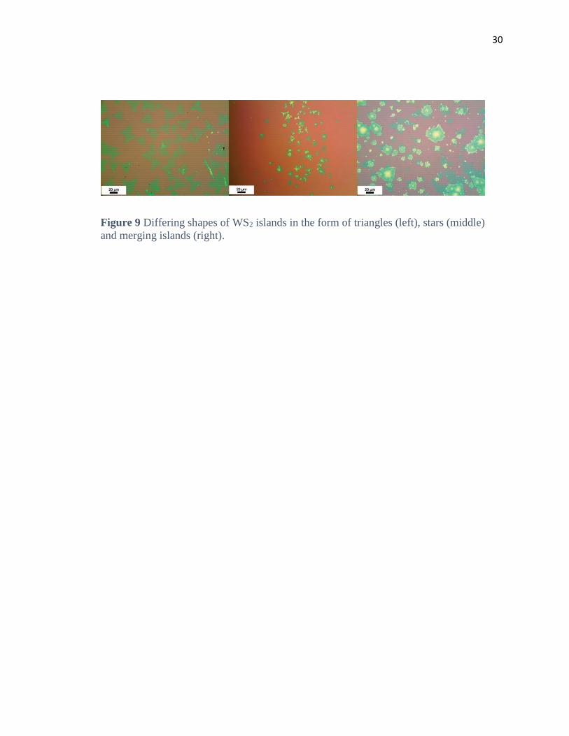
As in the case of MoS2, triangular islands are also the preferred morphology of
WS2 (Figure 9a). Other shapes seen in certain areas of the substrate are stars, hexagons
and merging islands, are shown in Figure 9b,c. Similarly, star shapes are seen when the
cool down time was too short and the reaction was not given enough time to grow, while
hexagons or merging islands are due to the over-deposition of the oxide. We tried to
investigate the deposition of the oxide after the initial CVD using only WO3 by taking a
Raman map, Figure 10, but after the second growth, the relationship between oxide
deposition and WS2 islands growth was unclear. As sulfurization is occurring, there is the
possibility of tungsten migrating further downstream and being redeposited elsewhere.
Thus far, all cases have been similar to the one shown in Figure 10 with areas of WO3
present, without WS2 growth. We are still considering how the growth of WS2 relates to
that of WO3 pre-deposited on the surface but it does not currently pose much of an issue
as large areas of monolayer triangular islands are forming.
30
Figure 9 Differing shapes of WS2 islands in the form of triangles (left), stars (middle)
and merging islands (right).
31
Figure 10 Raman map collected at 521 cm-1 of the area enclosed in a red rectangle shown
in the inset.

32
Subtle differences between MoS2 and WS2 is the mechanism of growth, although
it is more common for synthesis of many materials to occur at multiple nucleation points
we do not necessarily see that in the MoS2 growth very often but in the case of WS2 it is
far more common. For many trials, it is possible to see multiple small triangular islands
forming on the original monolayer, Figure 11. Since there are multiple nucleation sites, it
makes monolayer growth more difficult given that the focus has been to grow it off a
single nucleation site without a seed present, to compare the results properly to those of
MoS2. Unfortunately, we are not able to observe the growth process directly in our
furnace via SEM, transmission electron microscopy (TEM), or even optical microscopy.
It can be said that many of the monolayers grow from a single nucleation site because the
triangular shape appears unobstructed at the edges, see Figure 9a. This would mean that
the nucleation sites appearing on top of the monolayer are due to defects such as
dislocations or out-of-plane interstitial atoms that occur during the growth procedure.
These are caused by an excess sulfur or contact with unreacted WO3, creating an
additional site for nucleation to adsorb to.

33
20 µm
Figure 11 Multiple nucleation sites on the surface of a WS2 crystal.
34
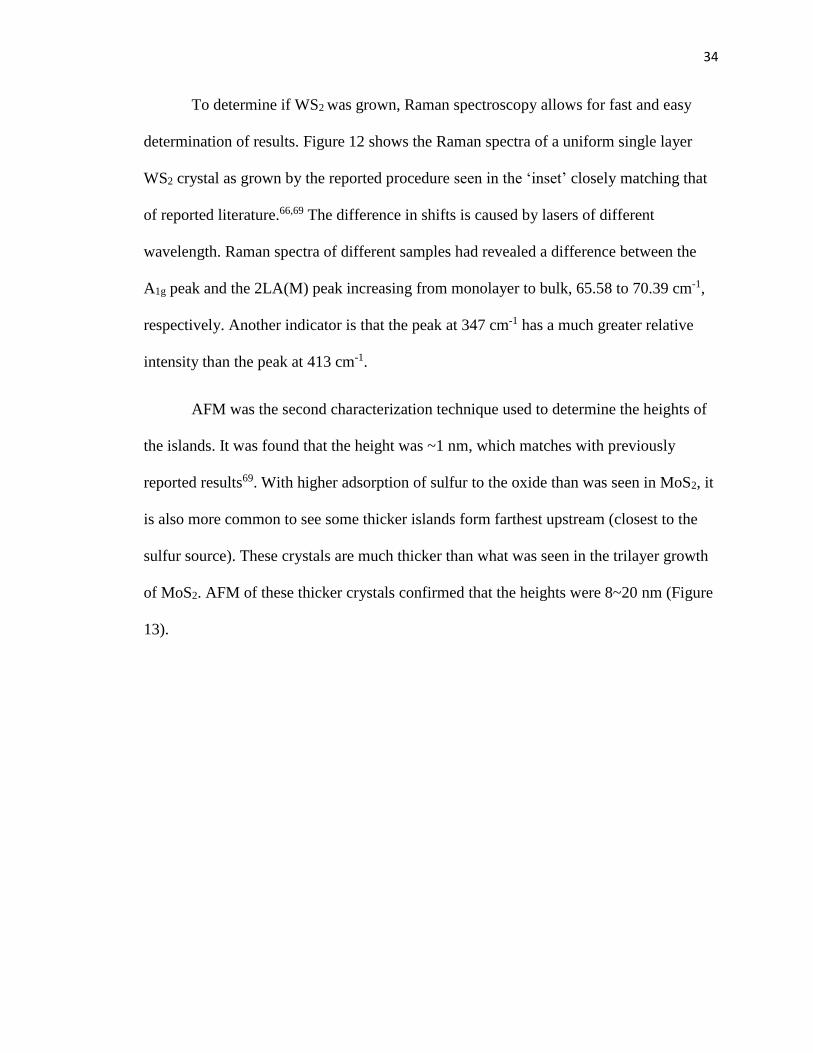
To determine if WS2 was grown, Raman spectroscopy allows for fast and easy
determination of results. Figure 12 shows the Raman spectra of a uniform single layer
WS2 crystal as grown by the reported procedure seen in the ‘inset’ closely matching that
of reported literature.66,69 The difference in shifts is caused by lasers of different
wavelength. Raman spectra of different samples had revealed a difference between the
A1g peak and the 2LA(M) peak increasing from monolayer to bulk, 65.58 to 70.39 cm-1,
respectively. Another indicator is that the peak at 347 cm-1 has a much greater relative
intensity than the peak at 413 cm-1.
AFM was the second characterization technique used to determine the heights of
the islands. It was found that the height was ~1 nm, which matches with previously
reported results69. With higher adsorption of sulfur to the oxide than was seen in MoS2, it
is also more common to see some thicker islands form farthest upstream (closest to the
sulfur source). These crystals are much thicker than what was seen in the trilayer growth
of MoS2. AFM of these thicker crystals confirmed that the heights were 8~20 nm (Figure
13).

35
100 200 300 400 500 600 700
0
2000
4000
6000
8000
10000 Monolayer 65.57
Bilayer 67.45
Multilayer 70.39
Inte
nsity (
a.u
.)
Raman Shift (cm-1)
Figure 12 Raman spectra of monolayer (1L), bilayer (2L) and multilayer (ML) WS2
crystals shown in the inset.

36
Figure 13 AFM showing the height of a thick multilayer WS2 crystal closest to the sulfur
source. Change in vertical height (Δh).
Δh = 17.42 nm

37
Finally, the electronic properties of the single layer WS2 crystals were measured.
The device seen in Figure 14 was one of the better devices fabricated. The mobility was
found to be moderately low in comparison to MoS2, Figure 14. Although the mobility is
~0.20 cm2 V-1 s-1, it is almost 20 times that of reported values for CVD grown WS2,
which were not reported to be any higher than 0.01 cm2 V-1 s-1.46 However, a number of
fabricated devices were nonfunctional due to the degradation of the SiO2 substrate, since
its melting point is close to that of WO3. The degradation of the substrate was associated
with the formation of nanoscopic holes, which caused high leakage currents and failure of
the devices. Transferring the WS2 flakes to a new substrate that was not subjected to high
temperature can drastically reduce leakage current. However, a new set of transfer related
defects can be introduced, such as trapping of transfer liquid or particles, leading to
mobility reduction. The measured mobilities are still higher than what has been reported.
In the future, transfer of the monolayer WS2 to a new substrate lacking holes
should help to ensure a larger sample size. While the growth modifications have not
drastically increased the mobilities, the results are encouraging as far as CVD grown WS2
is concerned. The gap between CVD synthesis and exfoliation techniques is shrinking.
Additionally, our two-part synthesis leads to appreciable monolayer growth, without the
requirement of a seed catalyst. In summary, WS2 synthesis still has much to improve
upon but with the limited data acquired, it is applicable towards more complex structures.

38
Figure 14 Optical image of single layer WS2 device (left). Mobility of WS2 device (right)
with an inset showing IDS-VSD dependencies measured at different gate voltages from -40
V to 40 V with a 20 V step.

39
CHAPTER 3: HETEROSTRUCTURES OF 2D MATERIALS
In recent years, there was a growing interest of heterostructures of 2D materials.
Stacking is one method of combining different 2D materials to form a heterostructure
with distinct properties. Stacking can be realized for materials obtained from both a top-
down or bottom-up approaches.
Many top-down methods involve individual exfoliation of the 2D materials, prior
to stacking, and then flakes are transferred one on top of another. The van der Waals
forces that hold graphene and other TMD materials together are strong enough that by
placing them in contact with one another they will not move. Some of the various
methods of mechanical transfer involve the use of polymers71,72 to lift one material off
from its substrate. Using some form of micromanipulator, the flake chosen for transfer
can then be placed at the desired location. After aligning the flake with a proper
orientation and position under an optical microscope or other objective lens, the flakes
can be brought together. This method also allows the freedom to change the alignment of
the materials and observe how different configurations change the interaction of the two
layers.73 Washing away of polymers is not a perfect process which leaves behind trace
amounts that will hinder further building. Recently, more advanced dry peel-off methods
have started to emerge to eliminate the use of polymers for such transfers.74–76
Bottom-up growth approaches are much more versatile in the number of
techniques available, ranging from CVD,77 pulsed laser deposition (PLD),78 vapor-liquid-
solid mechanism(VLS),79,80 atomic layer deposition (ALD),81 and others, provide a large
variety 2D materials that can be combined in various heterostructures. Currently, CVD
growth of 2D materials is mostly limited by the sensitivity of growth conditions used

40
since most have different growth parameters. While the bottom-up approaches are more
diverse, the top-down mechanical exfoliation is readily accessible as long as the bulk
crystals themselves are available.
Heterostructures do not necessarily need to be stacked vertically as described in
the above methods, but can also fused horizontally using the bottom-up approach. The
ability to create a structure without gaps between two materials or using a top-layer to
bridge two materials is a more recently developing idea.82 Many electronic properties are
determined by the edge of a material, which means that if that interface can be altered or
added to, so should the electronic properties.3,83 In this chapter, different forms of
heterostructures will be looked at via top-down and bottom-up approaches, while not
directly comparing the two methods on the same materials. Much of the following work
lays a foundation to grow and expand upon.
3.1 Graphene on boron nitride
Introduction
The field of graphene has seen more work done on it in recent years than most
other forms of research, but still many new ideas are still being generated as for its uses
or how to improve its current uses. The problems with many graphene devices on silicon
oxide (SiO2) are surface defects leading to disordered structure, charge trappings that can
cause shifts in the Dirac point,84 and impurity scattering.4 In order to remove surface
defects and help reduce charge trappings from the graphene it was thought to transfer the
graphene onto hexagonal boron nitride which is atomically smooth and free of dangling
bonds.12 Boron nitride has great thermal and dielectric stability,85 which will greatly help
to support properties of another material rather than inhibit them. Some of the issues with

41
transferring graphene onto different structures are polymer residues and the appearance
of wrinkles that develop due to the relaxation of the polymer once graphene has been
removed from the substrate.86 Different ideas have emerged to try and counter these
wrinkles, which involve either applying a thicker/secondary layer of polymer86 or using a
second polymer with more rigidity to it.72
Upon setting graphene atop boron nitride, the van der Waals interactions between
the two materials is strong enough to hold graphene in place. While the interactions are
strong, they are not as strong as the interactions that hold the bulk crystals of each
materials together due to lattice mismatching that is accommodated for by the van der
Waals gap.87,88 These van der Waals structures have been looked to expand graphene’s
uses beyond current limitations like it’s zero band gap89 and increasing its mobility.90
Overcoming these limitations, could result in more sophisticated electronic devices.
In this study, the goal was to first create a functional graphene boron nitride field
effect transistor, then study the functionalization of graphene on an insulator compared to
graphene on just SiO2. The second goal is to compare the same graphene flake placed on
top of boron nitride and on the SiO2 substrate. The second goal will help to ensure that
regardless of the material used, the properties demonstrated by that material will change.
Experimental Methods
Graphite flakes (Sigma Aldrich) were first exfoliated several times using Scotch
tape. Once determined to be thin enough, the tape was pressed onto p-doped silicon
substrates covered with a 300-nm-thick SiO2. The substrate was then heated to help
improve the adhesion of large area graphene flakes91 and then slowly peeled off. An
optical microscope was used to approximate the number of layers of graphene based
42
upon transparency and color. If a flake is thought to be single layer or of few layers, a
Raman spectrum was measured to confirm the number of layers, as Raman spectra of
single to few layer graphene has been well documented92–95 and can be quickly cross
referenced.
Polymethyl methacrylate in 4% anisole (PMMA-A4) was then drop-cast on the
substrate and spin coated on an SH-2 Magnetic Stirrer for 5 minutes at the max rate.
After spin coating, ~1 cm of PMMA was removed by scratching with a razor blade at the
edges furthest from the desired graphene flake to help later dissolve PMMA72. A piece of
PDMS is then cut to be slightly larger than the substrate and small holes are pierced near
the edges of the two sides that will line up with the areas of PMMA and exposed
substrate that were removed. These holes will help allow solvent to get under the PDMS
and dissolve the PMMA more easily as well as act as alignment markers once the
graphene has been removed from the substrate. The PDMS was then placed over the
PMMA as indicated above and gently pressed to ensure adhesion takes place evenly. The
PDMS/PMMA/graphene/substrate should then be placed directly into a 10% KOH
solution with the PDMS on top. After a short while the SiO2 will begin to dissolve,
releasing the PDMS/PMMA/graphene to be left floating on top of the solution. The
substrate can be safely picked up with tweezers at the corner of PDMS with holes to
avoid damaging desired graphene flake. It was then washed with water three times to
wash off most the remaining KOH leftover from the solution. The sample was then set on
a glass slide with the PDMS side in contact with glass to allow the sample to dry.
While the sample dries, a large yet thin boron nitride flake (Momentive) then
needs to be exfoliated in the same manner as graphene, indicated above. The major

43
difference is that it is more difficult to determine the thickness of boron nitride since
there has not been enough Raman work done to determine the thickness by differing
Raman wavenumbers, only shifts relating thin layers to bulk are generally seen.96 As a
fallback, AFM can then be used to determine thickness of boron nitride. While the boron
nitride does not necessarily need to be single layer for most of the goals of our
experiments, allowing for some leeway in thickness, but does need to be uniformly thick.
After confirmation of the thickness of the desired flake it was centered and refocused
under an optical microscope. Using a camera and TopView program, the flake can be
outlined to record the position and lowered out of focus without disturbing the x/y axial
stage controls.
Once the PDMS/PMMA/graphene was dry, the glass slide can then be attached
inverted to a secondary stage that has the capabilities to move in the x, y and z directions.
The graphene flake was focused using the secondary stage controls and shifted into the
outline of the boron nitride flake previously recorded in the program. Once the secondary
stage has been set into the outline, the microscope stage can then be raised slowly and
steadily, to not shift the x/y position. Upon contact of the substrate containing the boron
nitride flake and the glass slide holding PDMS/PMMA/graphene the stage should be
continued to be raised to promote better adhesion between the substrate and PMMA.
After 5 minutes the secondary stage was slowly raised to lift the substrate from the
microscope stage. The microscope stage can again be lowered out of focus and the
secondary stage refocused to determine if the graphene was in fact placed onto the boron
nitride. The secondary stage can then be moved and the sample lowered onto a hotplate at
65 ºC for 10 minutes to ensure better adhesion between the graphene and boron nitride.
44
After heating the sample is removed from the secondary stage and left to cool
slowly back to room temperature. The sample is finally washed with acetone to dissolve
the PMMA and release the graphene onto the boron nitride. Characterization of the van
der Waals heterostructure created is done by optical microscopy, Raman microscopy,
atomic force microscopy (AFM), and scanning electron microcopy (SEM).
Results and Discussion
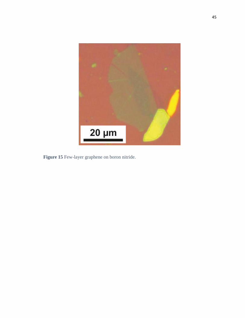
Successful transfer of graphene onto boron nitride is shown in Figure 15. The
graphene in this sample is not single layer but demonstrates a perfectly fit graphene
transfer and how the finished product should look. Because the graphene is completely
isolated from the Si/SiO2 substrate, that eliminating any potential surface interactions
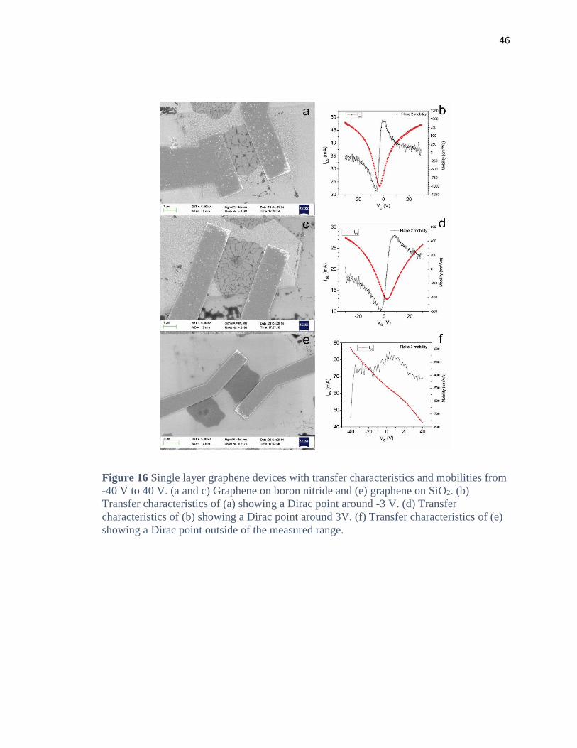
with SiO2. Figure 16a and b show two different single layer graphene flakes on the same
piece of boron nitride and Figure 16c shows a third single layer graphene flake on the
SiO2 ~200 µm away from the boron nitride flake. The transfer characteristics and
mobilities of each graphene flake are shown in Figures 16d-e. The graphene flakes that
are on boron nitride show Dirac points very close to zero whereas the graphene flake on
SiO2 shows a Dirac point that is drastically shifted away from zero. Since these flakes
were prepared on the same substrate at the same time there should be no difference in
how the devices were prepared meaning the boron nitride is eliminating charge trappings
on the surface.
45
Figure 15 Few-layer graphene on boron nitride.
46
Figure 16 Single layer graphene devices with transfer characteristics and mobilities from
-40 V to 40 V. (a and c) Graphene on boron nitride and (e) graphene on SiO2. (b)
Transfer characteristics of (a) showing a Dirac point around -3 V. (d) Transfer
characteristics of (b) showing a Dirac point around 3V. (f) Transfer characteristics of (e)
showing a Dirac point outside of the measured range.

47
If a device is positioned so that the area between the electrodes is completely on
boron nitride the results should be the same. Figure 17a shows a finished device where
the graphene was not completely placed fully on the boron nitride flake but the device
that was fabricated only measures the area between the graphene that is atop the boron
nitride. The mobility of the device can be seen to be ~2500 cm2 V-1 s-1, Figure 17d. (This
sample is not single layer graphene but few-layers. The measurements show reasonable
mobility for a few-layered device.) The next step after having created a FET of graphene
on boron nitride would be to then functionalize it since the Dirac point remains closer to
zero than that of flakes on SiO2 (Figure 16) helping to standardize shifts of different
functional groups. Since most devices are unable to attain a Dirac point at or near zero on
SiO2 then the shift of a Dirac point due to functionalization might result more from the
functional group affecting the SiO2 than the flakes in question.

48
Figure 17 Few-layer graphene device on boron nitride. (a) Optical image. (b) Transfer
characteristics of MoS2 device shown in (a). (c) ISD-VSD dependencies measured at
different gate voltages ranging from -40 V to 40 V with a 10 V step. (d) Mobility
calculation based on the transfer characteristics shown above.
a b
c d

49
While many studies have looked at the increase in electrical properties from
placing graphene onto boron nitride,12,97,98 there has been very little work done
demonstrating that difference using the exact same graphene flake. To make such a
comparison, a very long piece of few layer graphene (196 µm) was set on both boron
nitride and lead zirconate titanate (PZT). Two devices were fabricated using the same
graphene flake, as shown in Figure 18c and d. Figure 19 demonstrates how the electrical
properties changes from placing the device on boron nitride/PZT compared to being left
on the PZT. Because the boron nitride flake being used in this sample is so thick, it is
eliminating the hysteresis seen from switching of the PZT in graphene on PZT. It can be
seen that the drain-source current of graphene on boron nitride is also increased by a
factor of ~4, which relates to the graphene on boron nitride shown above in Figure 17
having similar drain-source current.
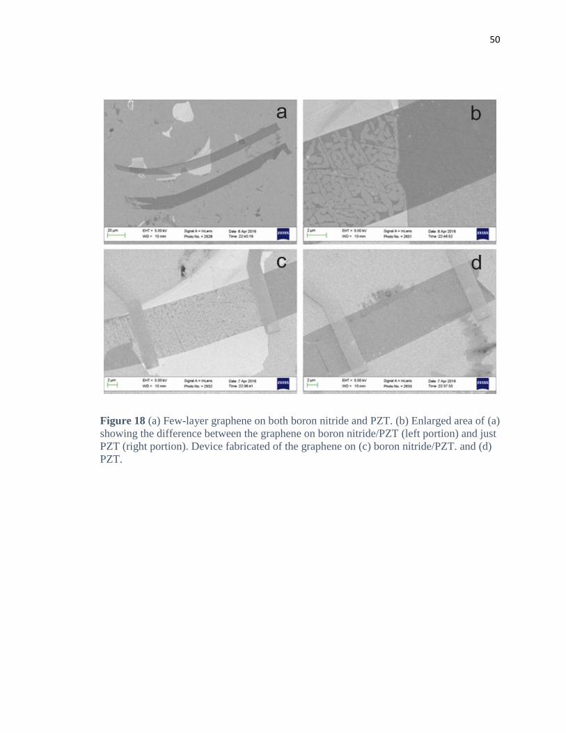
50
Figure 18 (a) Few-layer graphene on both boron nitride and PZT. (b) Enlarged area of (a)
showing the difference between the graphene on boron nitride/PZT (left portion) and just
PZT (right portion). Device fabricated of the graphene on (c) boron nitride/PZT. and (d)
PZT.

51
Figure 19 Transfer characteristics of Gr-PZT (left) and Gr-BN-PZT (right), where Gr
stands for graphene and BN stands for boron nitride.

52
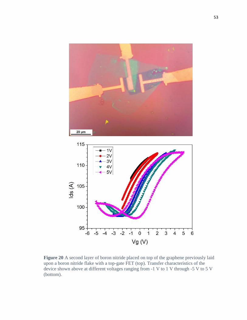
Future work would entail the addition of a second boron nitride flake on top of the
graphene already on boron nitride to act as a top-gate, that can be used in place of a band
gap to control switching99. Using the same procedure listed in the experimental section
for graphene transfer, the same was attempted for boron nitride. Figure 20 shows the first
completed sample of a boron nitride/graphene/boron nitride sample. As a preliminary
result, the structure shows the appearance of new wrinkles not previously seen after the
second transfer of boron nitride. This is likely due to liquids being trapped between each
set of layers as the wrinkles were not seen prior to lift off of the polymer. This effect has
also been seen in just the single transfer if washed or sonicated with an excess of acetone
when removing PMMA. It is not clear as to why acetone can get trapped in between
layers so easily during transfer of boron nitride but since graphene excels at preventing
liquids moving through it, it could help explain why so much liquid becomes trapped
after it squeezes between the layers. To determine if this preliminary result could lead to
better stability or lower operating voltages, a top-gate FET has been fabricated on the
graphene and the top boron nitride flake. The Dirac point of the materials is still close to
zero, seen here to be about -2 V, indicating less surface charge trappings that were seen
on SiO2. As seen in Figure 20, from -5 V to 5 V, a large hysteresis occurs similar to the
previous example where graphene was placed onto PZT. The BN/graphene/BN
heterostructures find emerging applications in high-performance nanoscale
optoelectronics,100 as well as flexible and transparent electronics.101
53
Figure 20 A second layer of boron nitride placed on top of the graphene previously laid
upon a boron nitride flake with a top-gate FET (top). Transfer characteristics of the
device shown above at different voltages ranging from -1 V to 1 V through -5 V to 5 V
(bottom).
54
3.2 Molybdenum disulfide on boron nitride
Introduction
With the work already completed on molybdenum disulfide (MoS2) discussed in
previous chapters and the work described in the previous section, the next step for MoS2
is to grow it on top of boron nitride. The idea is like that of placing graphene on top of
boron nitride to enhance the mobility90 and eliminate charge trapping.84 Similar work has
already been done with the exfoliation of MoS2 onto boron nitride, some going even
further of making a FET of these structures having graphene as the gate electrode
demonstrating larger mobilities101,102. The reduction of surface defects for growing MoS2
is also idealized by using boron nitride, since it is atomically flat and has very few
dangling bonds.12 It is unclear how many layers of boron nitride it should take to screen
the charged defects on the surface of SiO2. As such, it is reasonable to have a different
number of layers present on the same flake to determine at which layer the defects can be
screened. Another reason that boron nitride was chosen besides the previous work done is
due to its triangular growth mechanism seen when it is grown in smaller areas via
CVD.103 If both grow triangularly, the boron nitride should have a similar hexagonal
lattice to that of MoS2 allowing for more relaxed growth if the sizes of the unit cells are
compatible.
While CVD has become a promising route to explore new materials and their
growth patterns, there are still many different combinations of materials still undeveloped
or underdeveloped. A similar example to the work presented here can be seen in the work
of Dmitry Ruzmetov et al. on “Epitaxial Molybdenum Disulfide and Gallium Nitride,”
where they present similar results done on gallium nitride rather than boron nitride.104
55
Mitsuhiro Okada et al. report another experiment like our own using tungsten rather than
molybdenum to grow tungsten disulfide on boron nitride.105 In this section, we present
work reflecting the previously mentioned studies using our own techniques developed
previously and to the best of our knowledge, on a combination of
semiconductor/insulator materials not yet worked upon using the direct growth of the
semiconductor in CVD onto the insulating material.
Experimental Procedure
A substrate (~2 x 2 cm2) was cleaned for 10 minutes in acetone, 10 minutes in
deionized water, and 10 minutes in 2-propanol before treated with an UV ozone cleaner,
ProCleanerTM Plus system for 30 minutes. Boron nitride (Momentive) was then exfoliated
several times using adhesive tape. Once the flakes were determined to be thin enough, the
tape was pressed onto p-doped silicon substrates covered with 300 nm-thick SiO2. The
substrate was then heated to help improve the adhesion of larger area flakes91 and then
slowly peeled off. Flakes were first scrutinized using an optical microscope to determine
which flakes might be thin enough or contain enough different steps with enough space to
grow good single layer MoS2 triangles. The heights were then determined using AFM
before CVD could be done to ensure accurate height profiles of thin layered boron
nitride. This process was repeated twice onto smaller substrates (1 x 0.25 cm2).
Once the substrates contain good boron nitride flakes, 0.5-1 mg of molybdenum
(VI) oxide (99.5%, Sigma Aldrich) was placed into the center of a clean 40-mm quartz
boat. One of the smaller substrates (1 x 0.25 cm2) was placed with the SiO2 layer facing
away from the MoO3 (designated face-up) directly over the center of the MoO3 and the
second small substrate placed in the same orientation just downfield of the first. The
56
larger substrate (~2 x 2 cm2) was placed with the SiO2 layer facing toward the MoO3
(face-down) with one edge aligned over center of the MoO3. The quartz boat was then
loaded into a 2-inch quartz tube in a Lindberg Blue M tube furnace. A second quartz boat
was prepared with 50 mg of sulfur (99.998%, Sigma Aldrich) and placed ~35 cm
upstream of the MoO3, over the center of a hotplate.
The system was flushed with argon for 5 minutes and the growth procedure was
performed at atmospheric pressure with 100 sccm of argon flowing throughout the
growth procedure. The CVD procedure begins as the temperature goes up to 300 ºC over
30 minutes, remains at 300 ºC for 30 minutes, then climbs to 550 ºC over 30 minutes to
remove any water or surface contaminates that remained after cleaning. At 550 ºC the
temperature climbs to 805 ºC over 10 minutes, remains at 805 ºC for 5 minutes. The
cooling processes then begins with the furnace dropping to 550 ºC over 30 minutes
finally allowed to cool normally until 380 ºC before opening the furnace to cool back to
room temperature. To produce single layer MoS2 on boron nitride, the hotplate should be
turned to 250 ºC 2 minutes before the cooling process begins while still at 805 ºC.
Atomic force microscopy images were recorded using a Bruker Dimension Icon
atomic force microscope. Raman spectroscopy was performed using a Thermo Scientific
DXR Raman microscope with a 532 nm laser. Scanning electron microscopy (SEM)
images were taken using a Zeiss Supra 40 field-emission scanning electron microscope
using an in-lens detector at the accelerating voltage of 5 kV.
Results and Discussion
The growth procedure for MoS2 on SiO2 does not translate as well as initially
thought and thus leading to a slightly different experimental procedure than used in

57
Chapter 1. This is likely due to the differences in surfaces and nucleation. SiO2 was clean
and only contained surface defects. The nucleation of MoS2 could be anywhere and it
was not confined. Wafer scale films were not seen from the procedure described in
Chapter 1. In the case of boron nitride both of these details were an issue. The larger
problem of the two was the nucleation sites, because having flakes of boron nitride will
instantly generate multiple nucleation sites at the edges, whether it be between the SiO2
and a flake of boron nitride or individual layers of boron nitride within the same flake. As
can be seen from the optical image in Figure 21, the green area around the boron nitride
crystal (yellow) shows much more nucleation around the edges of the flake than other
parts of the substrate. The area highlighted in red from Figure 21 shows the large clusters
of nucleation between different layers. With more nucleation at edges between layers,
MoS2 also requires more space between the edges of two layers for triangular island
growth to occur. These two problems lead to decreasing the amount of cooldown time to
get smaller MoS2 triangles to fit better in areas between layers but with later sulfur
introduction time, i.e. turning the hotplate on later.

58
Figure 21 Optical image demonstrating MoS2 nucleation being favored at the edges of
boron nitride (left). SEM image of the optical image from the left panel of MoS2 growth
around and on top of boron nitride (right).

59
Since we predicted that growth should be better on boron nitride than just SiO2, it
can be reasoned that the lattice mismatch will be one of the largest contributing factor to
how well MoS2 can grow. The lattice also contributes to the directional growth of the
MoS2 on the boron nitride, it should grow in the same direction as the boron nitride’s
crystal structure and if it does happen epitaxial alignment should be seen consistently
throughout the crystal. A representative sample of MoS2 grown on thicker boron nitride
(>100 µm) is shown in Figure 22. The origin of alignment for triangles becomes clear
from the top and right edges, highlighted with a red and green line respectively. Of all the
MoS2 triangles present in Figure 22, >90% have two sides that align with both the red
and green lines shown.
The samples that do not have this same type of alignment pattern are the very thin
flakes of boron nitride, where surface defects of the SiO2 could still be more impactful
than the pristine surface of boron nitride. Figure 23 shows a thin boron nitride with MoS2
grown but it does not appear epitaxially aligned like the crystals from Figure 22. A
sample containing a boron nitride flake with thickness varying from very thin with
unaligned regions of MoS2 to the thicker regions of aligned growth is shown in Figure 24.
The AFM image in Figure 25 shows that the triangles grown in the thicker regions are in
fact single layer, which was also confirmed by Raman spectroscopy.
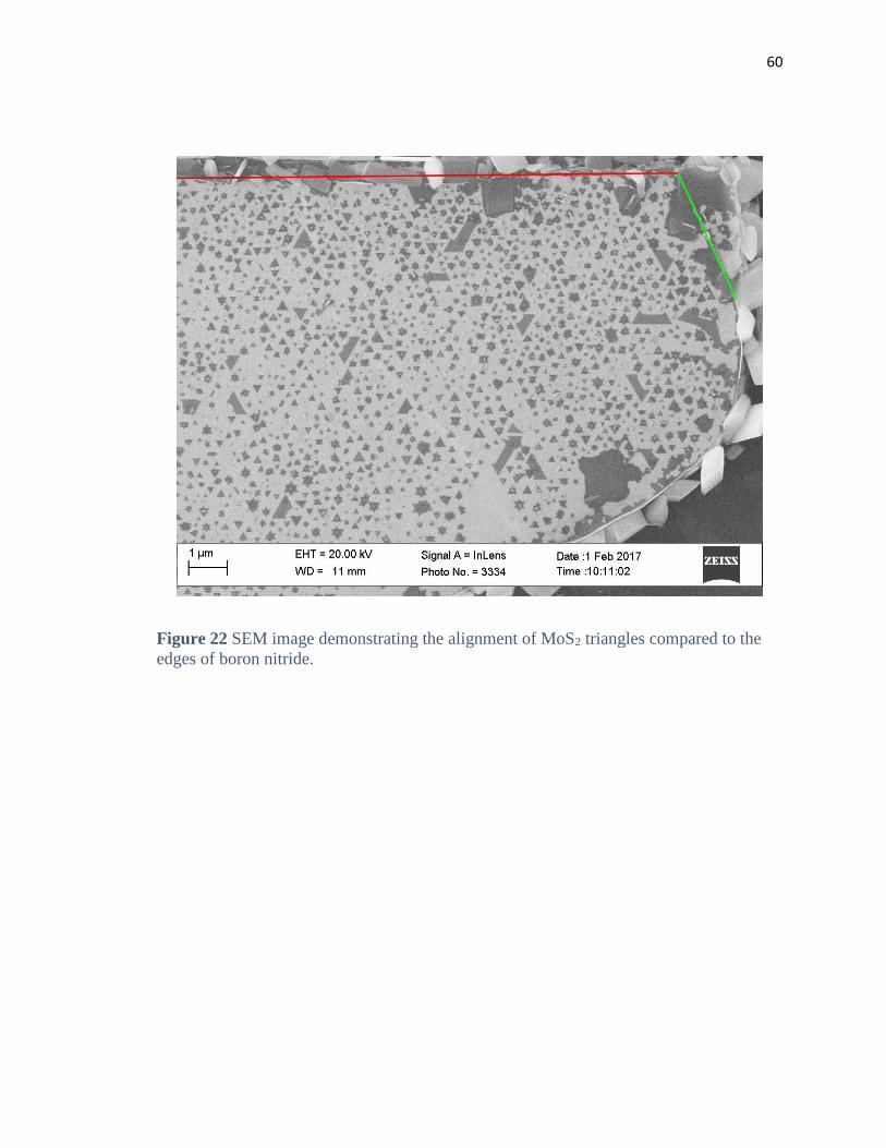
60
Figure 22 SEM image demonstrating the alignment of MoS2 triangles compared to the
edges of boron nitride.
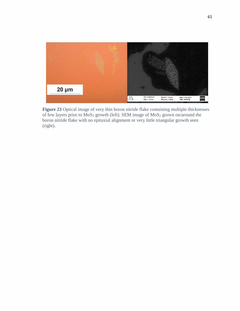
61
Figure 23 Optical image of very thin boron nitride flake containing multiple thicknesses
of few layers prior to MoS2 growth (left). SEM image of MoS2 grown on/around the
boron nitride flake with no epitaxial alignment or very little triangular growth seen
(right).
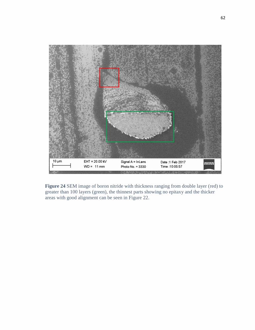
62
Figure 24 SEM image of boron nitride with thickness ranging from double layer (red) to
greater than 100 layers (green), the thinnest parts showing no epitaxy and the thicker
areas with good alignment can be seen in Figure 22.
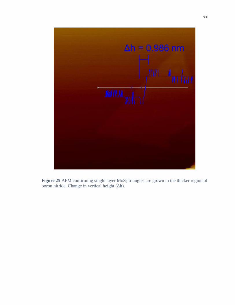
63
Figure 25 AFM confirming single layer MoS2 triangles are grown in the thicker region of
boron nitride. Change in vertical height (Δh).
Δh = 0.986 nm

64
3.3 Molybdenum disulfide/tungsten disulfide
Introduction
Strong interest TMDs and heterostructures resulted in the logical next step of
combining MoS2 and WS2 to create new heterostructures, with unique properties, not
seen in either material. While MoS2/WS2 heterostructures are not new, and much work
has already been underway with these structures in the vertical direction, one stacked on
top of the other,98,106–109 much less has been done in the lateral direction of these two
materials, in-plane with one another.98,110,111 Many of the challenges facing the lateral
heterostructures, not only MoS2/WS2 but others such as WS2/WSe2, MoS2/MoSe2 and
MoSe2/WSe2 are poor interfaces,112 lattice mismatch,82 or special precursors to help
create good contacts.111
Many of the aforementioned procedures have certain issues to overcome while
using single-step growth techniques giving rise to the idea to use a two-step process.
Having already established a two-step method for growing WS2 using tungsten oxide
deposition mentioned in Chapter 2, see experimental procedure, the foundation for
heterostructures using a two-step process was already in place. Kun Chen et al. also used
a similar idea of first growing an MoS2 island in an initial CVD and then growing a WS2
island around it in a second CVD to simplify the process of growing a lateral
heterostructure.110 Our idea and goal was originally to create a structure with a WS2
island grown using the pre-deposited WO3 to form a MoS2 island around it during the
second phase of CVD growth. While we attempt to grow both islands in the same CVD
cycle, it still utilizes a different method from the single-step growth techniques which

65
could allow for the expansion of growth for different materials. In this section, we present
findings similar to the goal previously mentioned but not with the originally desired
configuration.
Experimental Procedure
MoS2/WS2 crystals were grown on p-doped silicon substrates covered with a 300-
nm-thick SiO2 layer. The substrate was cleaned for 10 minutes in acetone, 10 minutes in
deionized water, and 10 minutes in 2-propanol before being treated in an UV ozone
cleaner, ProCleanerTM Plus system for 30 minutes. Once the substrate is clean, 1-2 mg of
WO3 (99.995%, Sigma Aldrich) was placed into the center of a clean 40-mm quartz boat.
The substrate (~4 x 2 cm2) was placed with the SiO2 layer facing toward the tungsten
source (face-down) with one edge aligned at the center of WO3. The quartz boat was then
loaded into a 2-inch quartz tube in a Lindberg Blue M tube furnace.
The system was flushed with argon and the growth procedure was performed
under vacuum with 100 sccm of argon flowing throughout the growth procedure at 1.5-
2.0 Torr. The CVD procedure starts as the temperature goes up to 300 ºC over 30
minutes, remains at 300 ºC for 30 minutes, then climbs to 550 ºC over 30 minutes to
remove any water or surface contaminates that remained after cleaning. At 550 ºC the
temperature climbs to 1100 ºC over 15 minutes, remains at 1100 ºC for 10 minutes, and
then is cooled normally until 420 ºC before opening the furnace to cool back to room
temperature.
The second CVD will be needed to ensure growth of the heterostructure of
MoS2/WS2. Once the CVD finishes, the substrate is then placed into the center of a
different clean quartz boat of the same size with 0.4-0.6 mg of MoO3 (99.5%, Sigma

66
Aldrich) in the center of it then loaded into new 2-inch quartz tube set in the furnace. A
third quartz boat was prepared with 40 mg of sulfur (99.998%, Sigma Aldrich) and
placed ~35 cm upstream of the center of the substrate, over the center of a hotplate.
The system was flushed with argon for 5 minutes and the growth procedure was
performed at atmospheric pressure with 100 sccm of argon flowing throughout the
growth procedure. The CVD procedure begins as the temperature goes up to 300 ºC over
30 minutes, remains at 300 ºC for 30 minutes, then climbs to 550 ºC over 30 minutes to
remove any water or surface contaminates that remained after cleaning. At 550 ºC the
temperature climbs to 805 ºC over 10 minutes, remains at 805 ºC for 5 minutes. The
cooling processes then begins with the furnace dropping to 550 ºC over 40 minutes
finally allowed to cool normally until 380 ºC before opening the furnace to cool back to
room temperature. To form single layer heterostructures, it was found that the hotplate
should be turned to 250 ºC as the cooling process begins.
Characterization of the MoS2/WS2 structures created was done via optical
microscopy, Raman microscopy, AFM, photoluminescence spectroscopy (PL), SEM and
transmission electron microscopy (TEM).
Results and Discussion
The inset in Figure 25 shows a heterostructure’s optical contrast within the same
triangular island. The differentiation between the two materials was first confirmed by
Raman spectroscopy. Figure 25 shows the Raman spectra of the areas highlighted in the
insert. The middle island is MoS2 and the outer island is WS2. Raman also confirmed
single layer MoS2 to be present because the difference between the 𝐸2𝑔1 peak and A1g
peak was ~19 cm-1. Similarly, the single layer WS2 was also confirmed with 532 nm the

67
peak at 351 cm-1, which should have had a higher intensity than the peak at 417 cm-1.
Raman maps were also created of several samples showing the major peak for MoS2 at
403 cm-1 and WS2 at 351 cm-1. Many of the maps created show similar results to the
Figure 26 shown below where the MoS2 is the predominant species while WS2 is
primarily seen along the edges. In some cases, though, WS2 can be seen in the center of
the MoS2, marking the growth of a second monolayer of WS2 on top of the MoS2.
To confirm that the Raman spectrum for these heterostructures is a result of the
individual materials and that the new structure is not interfering with the vibrational
frequencies, AFM was also done to confirm the number of layers. As can be observed
from Figure 28, the height profile across the center structure like the one shown in Figure
27 has very little to no change present when moving from the center to the outside. While
there should be some height discrepancy between the two different materials, it is not
easily seen in AFM because the single layer heights are so similar, MoS2 being 0.7 nm
and WS2 being 0.8 nm.
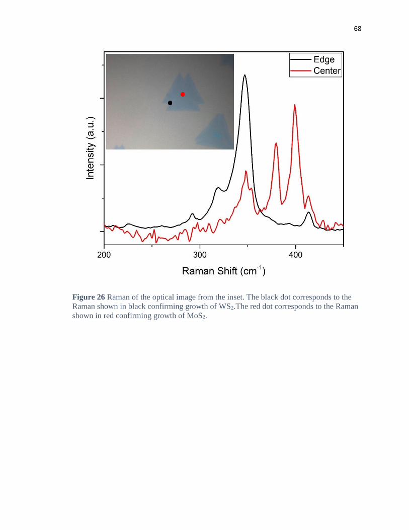
68
Figure 26 Raman of the optical image from the inset. The black dot corresponds to the
Raman shown in black confirming growth of WS2.The red dot corresponds to the Raman
shown in red confirming growth of MoS2.
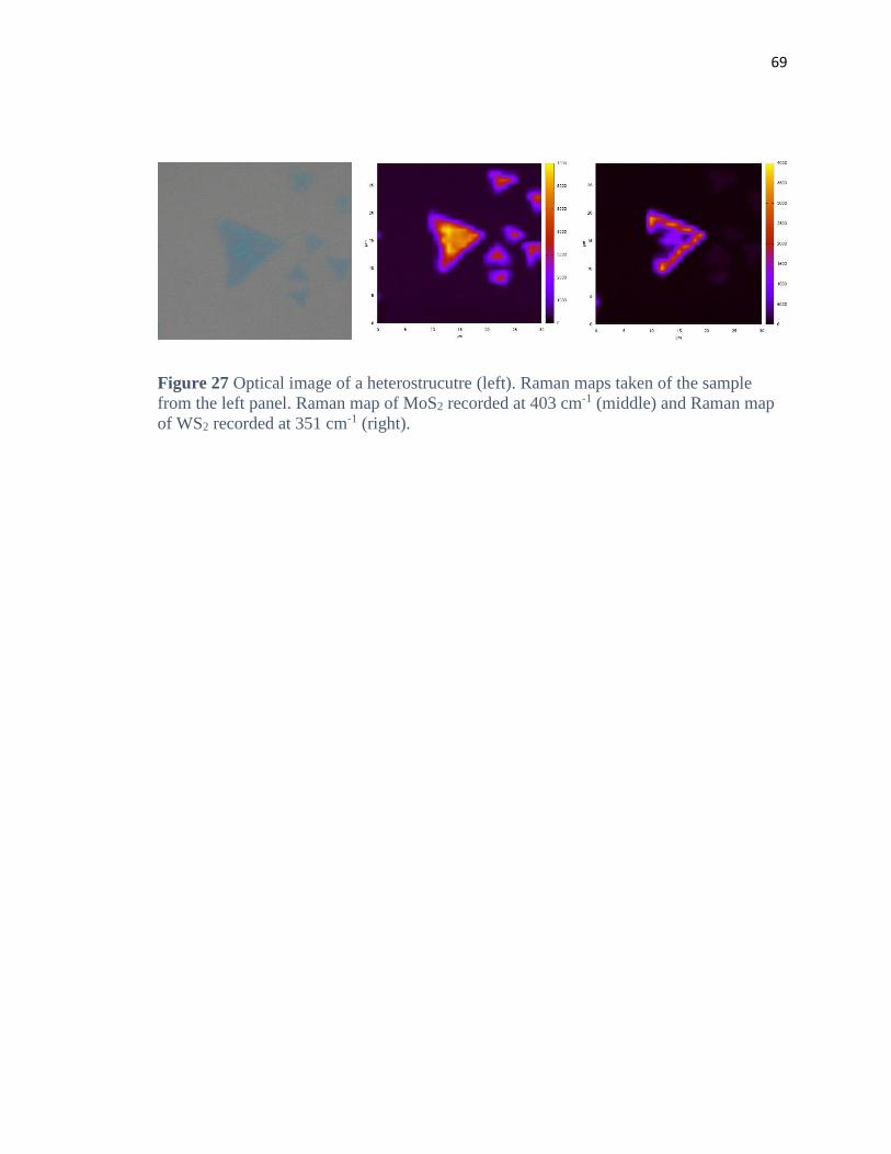
69
Figure 27 Optical image of a heterostrucutre (left). Raman maps taken of the sample
from the left panel. Raman map of MoS2 recorded at 403 cm-1 (middle) and Raman map
of WS2 recorded at 351 cm-1 (right).
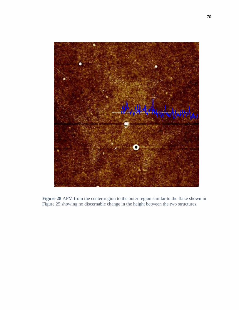
70
Figure 28 AFM from the center region to the outer region similar to the flake shown in
Figure 25 showing no discernable change in the height between the two structures.

71
PL of a similar area mapped by Raman is shown in Figure 29 for comparison of
the excitation. The outside of the islands appears brighter because the Cy5 filter cube
being used gives a better excitation of the WS2 wavelength, making the MoS2 in the
center appear dark. There is also a brighter area around the area that the two interfaces
meet, most likely due to higher electron density in these areas.
Electrical properties of the vertical species have been investigated thoroughly
using traditional FETs,108 femtosecond pump-probe spectroscopy,109 and Kelvin probe
force microscopy (KPFM)107 to observe interaction between van der Waals layers but
little work has been done thus far as to investigate the changes in electrical properties due
to the change as electrons flow laterally electron flow between the two. We present a
concept of how to measure the current through just MoS2, how it changes when flowing
through both MoS2 and WS2, and finally how it changes when flowing through WS2 with
a center portion of MoS2 separating two sides of WS2. The first device created is shown
in Figure 30, but the results of this experiment have been inconclusive thus far. The
problems previously observed in synthesis of WS2, where a large leakage current is
present, gives little validity to the current results most likely due to the extreme
conditions used in the synthesis process. The materials need to be transferred to a
different substrate for device fabrication, like in case of WS2 from Chapter 2. This should
eliminate the leakage current. This will leave an avenue for future work beyond what has
already been presented here.

72
Figure 29 PL map of the same sample shown in Figure 27.

73
Figure 30 Primary attempt at measuring electronic properties of an in-plane MoS2/WS2
heterostructure device.

74
Conclusion and Future Outlook
TMDs continue to be explored as complementary materials to graphene for a
variety of applications. There is also a growing interest in emerging heterostructures of
2D materials, which provide a more customizable way to design electronic properties. It
has been discussed here that monolayer, bilayer and trilayer MoS2 still have properties to
be explored and even more when placed onto the surface of another material. Alterations
to these materials could also prove useful, such as functionalization.
Much work still needs to be done to further improve CVD of WS2, as has been
done for MoS2 before it. We have shown a potential increase in the mobility compared to
current standards than have been produced. The development of WS2 could very easily
follow the same trend as MoS2 with its next step being the development of CVD
procedures for bilayer and trilayer materials to determine if the same trend can be
observed. Regardless of how the few layered materials behave, it could prove even more
useful to place and/or grow WS2 on other materials, such as boron nitride, to further
enhance the mobility, or possibly other properties as well. The combination of the two
materials, MoS2 and WS2 in the same plane could tailor electrical and optical properties
in much more specific ways than seen placing one atop of the other.
While TMDs enjoy the increasing popularity, there may still be some novelty left
to explore graphene in different heterostructures. In this work, graphene has been laid
upon boron nitride to boost its already amazing electronic properties. It was also shown
that the exact same graphene flake, does have better properties when placed onto boron

75
nitride. In the future work, a graphene flake on two different substrates can then be
functionalized to help accurately determine shifts in the Dirac point caused by different
functional groups.

76
References
1. Lee, C., Wei, X., Kysar, J. W. & Hone, J. Measurement of the elastic properties and intrinsic strength of monolayer graphene. Science 321, 385–388 (2008).
2. Eda, G., Fanchini, G. & Chhowalla, M. Large-area ultrathin films of reduced graphene oxide as a transparent and flexible electronic material. Nat. Nanotechnol. 3, 270–274 (2008).
3. Castro-Neto, A. H., Peres, N. M. R., Novoselov, K. S. & Geim, A. K. The electronic properties of graphene. Rev. Mod. Phys. 81, 109–162 (2009).
4. Chen, J. H., Jang, C., Xiao, S., Ishigami, M. & Fuhrer, M. S. Intrinsic and extrinsic performance limits of graphene devices on SiO2. Nat. Nanotechnol. 3, 206–209 (2008).
5. Xia, F., Farmer, D. B., Lin, Y. M. & Avouris, P. Graphene field-effect transistors with high on/off current ratio and large transport band gap at room temperature. Nano Lett. 10, 715–718 (2010).
6. Stankovich, S. et al. Graphene-based composite materials. Nature 442, 282–286 (2006).
7. Reina, A. et al. Large-scale pattern growth of graphene films for stretchable transparent electrodes. Nano Lett. 9, 30–35 (2009).
8. Nair, R. R. et al. Fine Structure Constant Defines Visual Transperency of Graphene. Science (80-. ). 320, 2008 (2008).
9. Orlita, M. et al. Approaching the dirac point in high-mobility multilayer epitaxial graphene. Phys. Rev. Lett. 101, 1–5 (2008).
10. Gmitra, M., Konschuh, S., Ertler, C., Ambrosch-Draxl, C. & Fabian, J. Band-structure topologies of graphene: Spin-orbit coupling effects from first principles. Phys. Rev. B - Condens. Matter Mater. Phys. 80, 2–7 (2009).
11. Zhang, Y. B., Tan, Y. W., Stormer, H. L. & Kim, P. Experimental observation of the quantum Hall effect and Berry’s phase in graphene. Nature 438, 201–204 (2005).
12. Dean, C. R. et al. Boron nitride substrates for high-quality graphene electronics. Nat. Nanotechnol. 5, 722–726 (2010).
13. Lu, J. et al. Order–disorder transition in a two-dimensional boron–carbon–nitride alloy. Nat. Commun. 4, 1–7 (2013).
14. R. R. Nair, W. C. Ren, R. Jalil, I. Riaz, V. G. Kravets, L. Britnell, P. Blake, F. Schedin, A. S. Mayorov, S. Yuan, M. I. Katsnelson, H. M. Cheng, W. Strupinski, L. G. Bulusheva, A. V. Okotrub, I. V. Grigorieva, A. N. Grigorenko, K. S. Novoselov, A. K. G. Fluorographene: a Two Dimensional Counterpart of Teflon R. Small 1–20 (2010).
15. Park, S. & Ruoff, R. S. Chemical methods for the production of graphenes. Nat Nano 4, 217–224 (2009).
16. Ci, L. et al. Atomic layers of hybridized boron nitride and graphene domains. Nat. Mater. 9, 430–435 (2010).

77
17. Butler, S. Z. et al. Progress, challenges, and opportunities in two-dimensional materials beyond graphene. ACS Nano 7, 2898–2926 (2013).
18. Two-dimensional, S. et al. Emerging Device Applications for. ACS Nano 8, 1102–1120 (2014).
19. Wang, Q. H., Kalantar-Zadeh, K., Kis, A., Coleman, J. N. & Strano, M. S. Electronics and optoelectronics of two-dimensional transition metal dichalcogenides. Nat. Nanotechnol. 7, 699–712 (2012).
20. Fiori, G. et al. Electronics based on two-dimensional materials. Nat. Nanotechnol. 9, 768–779 (2014).
21. Lv, R. et al. Transition metal dichalcogenides and beyond: Synthesis, properties, and applications of single- and few-layer nanosheets. Acc. Chem. Res. 48, 56–64 (2015).
22. Kobayashi, K. & Yamauchi, J. Electronic structure and scanning-tunneling-microscopy image of molybdenum dichalcogenide surfaces. Phys. Rev. B 51, 17085–17095 (1995).
23. Ding, Y. et al. First principles study of structural, vibrational and electronic properties of graphene-like MX2 (M=Mo, Nb, W, Ta; X=S, Se, Te) monolayers. Phys. B Condens. Matter 406, 2254–2260 (2011).
24. Transactions, I. & Devices, E. Performance Limits of Monolayer Transition Metal Dichalcogenide Transistors. 1–13 (2014). doi:10.1109/TED.2011.2159221
25. Kuc, A., Zibouche, N. & Heine, T. How does quantum confinement influence the electronic structure of transition metal sulfides TmS2. arXiv:1104.3670 1–11 (2011). doi:10.1103/PhysRevB.83.245213
26. Schwierz, F. Graphene transistors. Nat. Publ. Gr. 5, 487–496 (2031).
27. Mak, K., Lee, C., Hone, J., Shan, J. & Heinz, T. Atomically Thin MoS_{2}: A New Direct-Gap Semiconductor. Phys. Rev. Lett. 105, 136805 (2010).
28. Zhao, W. et al. Evolution of electronic structure in atomically thin sheets of ws 2 and wse2. ACS Nano 7, 791–797 (2013).
29. Zaumseil, J., Baldwin, K. W. & Rogers, J. A. Contact resistance in organic transistors that use source and drain electrodes formed by soft contact lamination. J. Appl. Phys. 93, 6117–6124 (2003).
30. Jena, D. & Konar, A. Enhancement of carrier mobility in semiconductor nanostructures by dielectric engineering. Phys. Rev. Lett. 98, 1–4 (2007).
31. S.V. Morozov, K.S. Novoselov, M.I. Katsnelson, F. Schedin, D.C. Elias, J.A. Jaszczak, A. K. G. Giant Intrinsic Carrier Mobilities in Graphene and Its Bilayer S.V. 4–8
32. RadisavljevicB et al. Single-layer MoS2 transistors. Nat Nano 6, 147–150 (2011).
33. Yoon, Y., Ganapathi, K. & Salahuddin, S. How good can monolayer MoS₂ transistors be? Nano Lett. 11, 3768–73 (2011).
34. Wu, W. et al. High mobility and high on / off ratio field-effect transistors based on chemical vapor deposited single-crystal MoS 2 grains. Appl. Phys. Lett. 102, 142106

78
(2013).
35. Late, D. J. et al. Sensing behavior of atomically thin-layered MoS2 transistors. ACS Nano 7, 4879–4891 (2013).
36. Lopez-Sanchez, O., Lembke, D., Kayci, M., Radenovic, A. & Kis, A. Ultrasensitive photodetectors based on monolayer MoS2. Nat. Nanotechnol. 8, 497–501 (2013).
37. Lipatov, A., Sharma, P., Gruverman, A., Sinitskii, A. & Alexey Lipatov,† Pankaj Sharma,‡ Alexei Gruverman,‡, and A. S. Optoelectrical Molybdenum Disulfide (MoS2)-Ferroelectric Memories. Am. Chem. Soc. 9, 8089–8098 (2015).
38. Du, G. et al. Superior stability and high capacity of restacked molybdenum disulfide as anode material for lithium ion batteries. Chem. Commun. 46, 1106–1108 (2010).
39. Frindt, R. F. Single crystals of MoS2 several molecular layers thick. J. Appl. Phys. 37, 1928–1929 (1966).
40. M, C. Photoluminescence from Chemically Exfoliated MoS2. Nano Lett. 12, 526 (2012).
41. Coleman, J. N. et al. Two-Dimensional Nanosheets Produced by Liquid Exfoliation of Layered Materials. Science (80-. ). 331, 568–571 (2011).
42. Smith, R. J. et al. Large-scale exfoliation of inorganic layered compounds in aqueous surfactant solutions. Adv. Mater. 23, 3944–3948 (2011).
43. Bao, W. et al. Visualizing nanoscale excitonic relaxation properties of disordered edges and grain boundaries in monolayer molybdenum disulfide. Nat. Commun. 6, 1–7 (2015).
44. Lee, Y. H. et al. Synthesis of large-area MoS2 atomic layers with chemical vapor deposition. Adv Mater 24, 2320–2325 (2012).
45. Najmaei, S. et al. Vapor Phase Growth and Grain Boundary Structure of Molybdenum Disulfide Atomic Layers. arXiv.org cond-m, 754–759 (2013).
46. Lee, Y. et al. Synthesis and Transfer of Single Layer Transition Metal Disulfides on Diverse Surfaces Synthesis and Transfer of Single Layer Transition Metal Disulfides on Diverse Surfaces. Nano Lett. 13, 1852–1857 (2013).
47. van der Zande, A. M. et al. Grains and grain boundaries in highly crystalline monolayer molybdenum disulphide. Nat. Mater. 12, 554–61 (2013).
48. Wang, S. S. et al. Shape Evolution of Monolayer MoS2 Crystals Grown by Chemical Vapor Deposition. Chem. Mater. 26, 6371–6379 (2014).
49. Yu, Y. et al. Controlled scalable synthesis of uniform, high-quality monolayer and few-layer MoS2 films. Sci. Rep. 3, 1866 (2013).
50. Liu, Z., Najmaei, S., Zhan, Y., Ajayan, P. M. & Lou, J. Large Area Vapor Phase Growth and 2D Engineering of Atomic Layers. (2012).
51. Wu, S. et al. Vapor-solid growth of high optical quality MoS2 monolayers with near-unity valley polarization. ACS Nano 7, 2768–2772 (2013).
52. Liu, B. K., Zhang, W., Lee, Y. & Lin, Y. Supporting Materials Growth of Large-Area and

79
Highly Crystalline MoS 2 Thin Layers on Insulating Substrates. 2, 1–9
53. Kang, K. et al. High-mobility three-atom-thick semiconducting films with wafer-scale homogeneity. Nature 520, 656–660 (2015).
54. Lin, Z. et al. Facile synthesis of MoS2 and MoxW1-xS2 triangular monolayers. APL Mater. 2, 92514 (2014).
55. Lauritsen, J. V. et al. Size-dependent structure of MoS2 nanocrystals. Nat. Nanotechnol. 2, 53 (2007).
56. Ming Xia, Bo Li, K. Y., Giovanni Capellini, GangNiu, Yongji Gong, WuZhou, P. M. A. & Xie, and Y.-H. Spectroscopic Signatures of AA0 and AB Stacking of Chemical Vapor Deposited Bilayer MoS2. (2009). doi:10.1007/3-540-35375-5
57. Liu, K. et al. Evolution of Interlayer Coupling in Twisted MoS2 Bilayers. arXiv Prepr. arXiv … 5, 1–6 (2014).
58. Shi, Y., Li, H. & Li, L.-J. Recent advances in controlled synthesis of two-dimensional transition metal dichalcogenides via vapour deposition techniques. Chem. Soc. Rev. 44, 2744–56 (2015).
59. Lipatov, A. et al. Few-layer titanium trisulfide (TiS3) field-effect transistors. Nanoscale 12291–12296 (2015). doi:10.1039/C5NR01895A
60. Li, H. et al. From bulk to monolayer MoS 2: Evolution of Raman scattering. Adv. Funct. Mater. 22, 1385–1390 (2012).
61. Lee, C. et al. Anomalous lattice vibrations of single-and few-layer MoS2. ACS Nano 4, 2695–700 (2010).
62. Sinitskii, A., Dimiev, A., Kosynkin, D. V. & Tour, J. M. Graphene nanoribbon devices produced by oxidative unzipping of carbon nanotubes. ACS Nano 4, 5405–5413 (2010).
63. Britnell, L. et al. Field ‐ effect tunneling transistor based on vertical graphene heterostructures. 1–11
64. Zhang, Y. et al. Controlled Growth of High-Quality Monolayer WS 2 Layers on Sapphire. ACS Nano 7, 8963–8971 (2013).
65. Gutierrez, H. R. et al. Extraordinary room-temperature photoluminescence in WS2 triangular monolayers. Nano Lett. 13, 3447–3454 (2012).
66. Berkdemir, A. et al. Identification of individual and few layers of WS2 using Raman spectroscopy. Sci. Rep. 3, 1755 (2013).
67. Lan, C., Li, C., Yin, Y. & Liu, Y. Large-area synthesis of monolayer WS 2 and its ambient-sensitive photo-detecting performance. Nanoscale 7, 5974–5980 (2015).
68. Hwang, W. S. et al. Transistors with chemically synthesized layered semiconductor WS2 exhibiting 10^5 room temperature modulation and ambipolar behabvior. Appl. Phys. Lett. 13107, 101 (2012).
69. Song, J. et al. Conformal Synthesis of Tungsten Disul fi de Nanosheets Using Atomic Layer Deposition. ACS Nano 7, 11333–11340 (2013).

80
70. Physics, E. & Engineering, I. High Performance Field-Effect Transistor Based on Multilayer Tungsten Disulfide Xue Liu † ¶ , Jin Hu † ¶ , Chunlei Yue † , Della Fera, Nicholas D † , Yun Ling ‡§ , Zhiqiang Mao † , Jiang Wei † * † ‡.
71. Geim, A. K. & Grigorieva, I. V. Van der Waals heterostructures. Nature 499, 419–425 (2014).
72. Li, H. et al. A Universal, Rapid Method for Clean Transfer of Nanostructures onto Various Substrates. ACS Nano 8, 6563–6570 (2014).
73. Woods, C., Britnell, L. & Eckmann, A. Commensurate-incommensurate transition for graphene on hexagonal boron nitride. arXiv Prepr. arXiv … (2014).
74. Withers, F. et al. Light-emitting diodes by band-structure engineering in van der Waals heterostructures. Nat Mater 14, 301–306 (2015).
75. Wang, L. et al. One-dimensional electrical contact to a two-dimensional material. Science (80-. ). 342, 614–7 (2013).
76. Kretinin, A. V et al. Electronic properties of graphene encapsulated with different 2D atomic crystals. Nano Lett. 1–19 (2014). doi:10.1021/nl5006542
77. Ambacher, O. et al. Two-dimensional electron gases induced by spontaneous and piezoelectric polarization charges in N- and Ga-face AlGaN/GaN heterostructures. J. Appl. Phys. 85, 3222 (1999).
78. J. Wang, J. B. Neaton, H. Zheng, V. Nagarajan, S. B. Ogale, D. Viehland, V.Venugopalan, D.G. Schlom, U. V.Waghmare, N. A. Hill, and K.M. Rabe, M.Wuttig, and R. R. Epitaxial BiFeO3Multiferroic Thin FilmHeterostructures. (2003).
79. Duan, X. F. & Lieber, C. M. General synthesis of compound semiconductor nanowires. Adv. Mater. 12, 298–302 (2000).
80. Lauhon, L. J., Gudiksen, M. S., Wang, D. & Lieber, C. M. Epitaxial core-shell and core-multishell nanowire heterostructures. Nature 420, 57–61 (2002).
81. Tan, L. K. et al. Atomic layer deposition of a MoS₂ film. Nanoscale 6, 10584–8 (2014).
82. Huang, C. et al. Lateral heterojunctions within monolayer MoSe2–WSe2 semiconductors. Nat. Mater. 13, 1–6 (2014).
83. Kibsgaard, J., Chen, Z., Reinecke, B. N. & Jaramillo, T. F. Engineering the surface structure of MoS2 to preferentially expose active edge sites for electrocatalysis. Nat. Mater. 11, 963–969 (2012).
84. Chen, J. H. et al. Printed graphene circuits. Adv. Mater. 19, 3623–3627 (2007).
85. Kim, K. K. K. K. K. et al. Synthesis and Characterization of Hexagonal Boron Nitride Film as a Dielectric Layer for Graphene Devices. ACS Nano 6, 8583–8590 (2012).
86. Liang, X. et al. Toward clean and crackless transfer of graphene. ACS Nano 5, 9144–9153 (2011).
87. Ma, Y., Dai, Y., Guo, M., Niu, C. & Huang, B. Graphene adhesion on MoS2 monolayer: An ab initio study. Nanoscale 3, 3883–3887 (2011).

81
88. Shi, Y. et al. van der Waals Epitaxy of MoS 2 Layers Using Graphene As Growth Templates. Nano Lett. 12, 2784–2791 (2012).
89. Giovannetti, G., Khomyakov, P. A., Brocks, G., Kelly, P. J. & Brink, J. Van Den. Substrate-induced bandgap in graphene on hexagonal boron nitride. Phys. Rev. B 76, 73103 (2007).
90. Zomer, P. J., Dash, S. P., Tombros, N. & van Wees, B. J. A new transfer technique for high mobility graphene devices on commercially available hexagonal boron nitride. 10–12 (2011). doi:10.1063/1.3665405
91. Huang, Y. et al. Reliable Exfoliation of Large-Area High-Quality Flakes of Graphene and Other Two-Dimensional Materials. ACS Nano 9, 10612–10620 (2015).
92. Ferrari, A. C. et al. Raman spectrum of graphene and graphene layers. Phys. Rev. Lett. 97, 1–4 (2006).
93. Ferrari, A. C. & Basko, D. M. Raman spectroscopy as a versatile tool for studying the properties of graphene. Nat Nanotechnol 8, 235–246 (2013).
94. Graf, D. & Ensslin, K. Spatially Resolved Raman Spectroscopy of Single- and Few-Layer Graphene. Solid State Phys. 1–6 (2008). doi:10.1021/nl061702a
95. Mohiuddin, T. M. G. et al. Uniaxial strain in graphene by Raman spectroscopy: G peak splitting, Grüneisen parameters, and sample orientation. Phys. Rev. B - Condens. Matter Mater. Phys. 79, (2009).
96. R. V. Gorbachev, I. Riaz, R. R. Nair, R. Jalil, L. Britnell, B. D. Belle, E. W. Hill, K. S. Novoselov, K. Watanabe, T. Taniguchi, A. K. Geim, P. B. Hunting for Monolayer Boron Nitride: Optical and Raman Signatures R. Harvard Bus. Sch. Cases 1 (2010). doi:10.1002/smll.201001628
97. Levendorf, M. P. et al. Graphene and boron nitride lateral heterostructures for atomically thin circuitry. Nature 488, 627–632 (2012).
98. Gong, Y. et al. Vertical and in-plane heterostructures from WS2/MoS2 monolayers. Nat Mater 13, 1135–1142 (2014).
99. Oostinga, J. B., Heersche, H. B., Liu, X., Morpurgo, A. F. & Vandersypen, L. M. K. Gate-induced insulating state in bilayer graphene devices. Nat. Mater. 7, 151–157 (2008).
100. Hyun Jeong, S. B., Hye Min Oh, Hyeon Jun Jeong, Sung-Jin An, G. H. H., Kim, H. & Ki Kang Kim, Jin Cheol Park, Young Hee Lee, Gilles Lerondel, and M. S. J. Semiconductor-Insulator- Semiconductor Diode Consisting of Monolayer MoS2,h‑BN, and GaN Heterostructure. 10032–10038 (2015). doi:10.1021/acsnano.5b04233
101. Lee, G.-H. et al. Flexible and Transparent MoS 2 Field-Effect Transistors on Hexagonal Boron Nitride-Graphene Heterostructures. ACS Nano 7, 7931–7936 (2013).
102. Lee, G.-H. et al. Highly Stable, Dual-Gated MoS 2 Transistors Encapsulated by Hexagonal Boron Nitride with Gate-Controllable Contact, Resistance, and Threshold Voltage. ACS Nano 9, 7019–7026 (2015).
103. Wang, L. et al. Monolayer hexagonal boron nitride films with large domain size and clean interface for enhancing the mobility of graphene-based field-effect transistors. Adv.

82
Mater. 26, 1559–1564 (2014).
104. Ruzmetov, D. et al. Vertical 2D/3D Semiconductor Heterostructures Based on Epitaxial Molybdenum Disulfide and Gallium Nitride. ACS Nano 10, 3580–3588 (2016).
105. Okada, M. et al. Direct chemical vapor deposition growth of WS2 atomic layers on hexagonal boron nitride. ACS Nano 8, 8273–8277 (2014).
106. Yu, Y. et al. Equally Efficient Interlayer Exciton Relaxation and Improved Absorption in Epitaxial and Non-epitaxial MoS2 / WS2 Heterostructures Equally Efficient Interlayer Exciton Relaxation and Improved Absorption in Epitaxial and Non-epitaxial MoS 2 / WS 2 Heterost. Nano Lett. 15, 4 (2015).
107. Chen, K. et al. Electronic Properties of MoS2-WS2 Heterostructures Synthesized with Two-Step Lateral Epitaxial Strategy. ACS Nano 9868–9876 (2015). doi:10.1021/acsnano.5b03188
108. Huo, N. et al. Novel and enhanced optoelectronic performances of multilayer MoS2 -WS2 heterostructure transistors. Adv. Funct. Mater. 24, 7025–7031 (2014).
109. Hong, X. et al. Ultrafast charge transfer in atomically thin MoS2/WS2 heterostructures. Nat. Nanotechnol. 9, 1–5 (2014).
110. Koåmider, K. & Fernández-Rossier, J. Electronic properties of the MoS2-WS2 heterojunction. Phys. Rev. B - Condens. Matter Mater. Phys. 87, 41–44 (2013).
111. Zhang, X. Q., Lin, C. H., Tseng, Y. W., Huang, K. H. & Lee, Y. H. Synthesis of lateral heterostructures of semiconducting atomic layers. Nano Lett. 15, 410–415 (2015).
112. Duan, X. et al. Lateral epitaxial growth of two-dimensional layered semiconductor heterojunctions. Nat Nanotechnol 9, 1024–1030 (2014).


![Low-Dimensional Te-Based … · vapor-phase deposition, [16 ] the solvothermal method, [18 ] and the electrochemical deposition method. [19 ] Specifi cally, some unique growth mechanisms](https://img.pdfslide.us/doc/110x75/607d5e47b1a3733eaa4802dd/low-dimensional-te-based-vapor-phase-deposition-16-the-solvothermal-method.jpg)