Embed Size (px)
Citation preview

The Pennsylvania State University
The Graduate School
METALORGANIC CHEMICAL VAPOR DEPOSITION OF TWO-
DIMENSIONAL LAYERED CHALCOGENIDES
A Dissertation in
Materials Science and Engineering
by
Xiaotian Zhang
2019 Xiaotian Zhang
Submitted in Partial Fulfillment
of the Requirements
for the Degree of
Doctor of Philosophy
August 2019

The dissertation of Xiaotian Zhang was reviewed and approved* by the following:
Joan M. Redwing
Professor of Materials Science and Engineering
Associate director of the Materials Research Institute
Director of the 2D Crystal Consortium – Materials Innovation Platform
Dissertation Advisor
Chair of Committee
Joshua A. Robinson
Associate professor of Materials Science and Engineering
Associate director of Center for Two-Dimensional and Layered Materials
Director of User Programs of the 2D Crystal Consortium – Materials
Innovation Platform
Thomas N. Jackson
Robert E. Kirby Chair Professor of Electrical Engineering
Susan B. Sinnott
Professor of Materials Science and Engineering and Chemistry
Head of the Department of Materials Science and Engineering
Suzanne E. Mohney
Professor of Materials Science and Engineering and Electrical Engineering
Chair of Intercollege Graduate Degree Program in Materials Science and
Engineering
*Signatures are on file in the Graduate School

iii
ABSTRACT
Two dimensional (2D) materials have attracted wide interest because of their
layered crystal structures and anisotropic properties which leads to potential new
diversity of function in nanoelectronics, photonics, sensing, energy storage, and
optoelectronics. Among them, the family of 2D layered chalcogenides (2DLCs) including
transition metal dichalcogenides (TMDs) (in the form of MX2 where M=Mo, W, etc. and
X=S, Se, Te) and group IIIA metal chalcogenides (MCs) (typically in the form of MX
and M2X3 where M=Ga, In and X=S, Se) have been a focus of increasing interest due to
their number of intriguing properties. Monolayer TMDs have exhibited unique optical
and electical properties such as indirect-to-direct band gap, spin valley polarization,
interlayer exciton coupling, single photon emission. On the other hand, monolayer and
few-layer MCs also demonstrate novel properties such as high carrier mobilities (~1000
cm2/Vs) for γ-InSe and ultrasensitive photoresponse as well as in-plane or/and out-of-
plane ferroelectricity for α- and β-In2Se3. Therefore, the rapid development of device
technologies based on 2DLCs causes increasing demand for synthesis of high-quality
wafer-scale single crystal monolayer and few layer films.
Among techniques for thin film deposition, gas source chemical vapor deposition
(CVD) /metalorganic CVD (MOCVD) is emerging as a promising method for wafer-
scale growth of TMDs and related 2DLCs due to the ability to grow at high temperatures
(>700 ℃), moderate reactor pressures (10-700 Torr) and high chalcogen/metal gas phase
ratios which are needed to achieve epitaxy and film stoichiometry. However, the effects
of precursor chemistry on film properties have not been examined and methods to
iv
achieve uniform, fully coalesced epitaxial monolayer TMD films are required. In
addition, the growth of group III MCs by MOCVD is largely unexplored.
This dissertation focuses on a comprehensive study of gas source CVD/MOCVD
growth of WSe2 and In2Se3 which represent the TMDs and group IIIA MCs, respectively.
In the MOCVD growth of WSe2, a defective graphene layer was found to form on the
sapphire substrate simultaneously at high growth temperature and high Se:W ratio when
using tungsten hexacarbonyl (W(CO)6) and dimethyl selenide ((CH3)2Se, DMSe) as
precursors. The graphene layer alters the surface energy of the substrate reducing the
lateral growth and coalescence of WSe2 domains. By switching to hydrogen selenide
(H2Se) instead of DMSe, the defective graphene layer was eliminated and a multi-step
diffusion-mediated process was developed for the epitaxial growth of coalesced
monolayer WSe2 films on c-plane sapphire. The multi-step process consists of an initial
nucleation step which used a high W(CO)6 flow rate along with H2Se at 800℃ and 700
Torr to promote nucleation. The W(CO)6 was then switched out of the reactor and the
sample was annealed in H2Se to promote surface diffusion of tungsten-containing species
to form oriented WSe2 islands with uniform size and controlled density. The W(CO)6 was
then switched back into the reactor at a lower flow rate to suppress further nucleation and
laterally grow the WSe2 islands to form a fully coalesced monolayer film in less than one
hour. Reflection high energy electron diffraction (RHEED) and in-plane X-ray diffraction
(XRD) measurements further confirm that the coalesced WSe2 monolayer film is
epitaxially oriented on sapphire as [1010] WSe2 ‖ [1010] α-Al2O3. High resolution
annular dark field scanning transmission electron microscopy (ADF-STEM) and selected

v
area diffraction analysis of WSe2 removed from the sapphire also indicate that the films
are predominately single crystal with inversion domain boundaries (IDBs) that result
from merging of 0º and 60º oriented domains. The process also provides fundamental
insights into the 2D growth mechanism. The evolution of domain size and cluster density
with annealing time follows a 2D ripening process, enabling an estimate of the tungsten-
species surface diffusivity of 1.2×10⁻¹⁴ cm2/s. The lateral growth rate of domains was
found to be relatively independent of substrate temperature over the range of 700-900 oC
suggesting a mass transport limited process, however, the domain shape (triangular
versus truncated triangular) varied with temperature over this same range due to local
variations in the Se:W adatom ratio. The results provide an important step toward atomic
level control of the epitaxial growth of WSe2 monolayers in a scalable process that is
suitable for large area device fabrication.
To pursue the scalable growth of “single crystal” TMDs, a defect-controlled
approach for the nucleation and epitaxial growth of WSe2 on hexagonal boron nitride
(hBN) was investigated. The WSe2 domains exhibit a preferred orientation of over 95%
leading to a reduced density of IDBs upon coalescence. First-principles calculations and
experimental studies as a function of growth conditions and substrate pre-treatment
confirm that WSe2 nucleation density and orientation are controlled by the hBN surface
defect density rather than thermodynamic factors. Detailed TEM analysis provides
support for the role of single-atom vacancies on the hBN surface which trap W atoms and
break surface symmetry leading to a reduced formation energy for one orientation of
WSe2 domains. Through careful control of nucleation and extended lateral growth time,

vi
fully coalesced WSe2 monolayer films on hBN were achieved. Low temperature
photoluminescence (PL) measurements and transport measurements of backgated field
effect transistor (FET) devices fabricated on WSe2/hBN films show improved optical and
electrical properties compared to films grown on sapphire under similar conditions. These
results reveal an important nucleation mechanism for epitaxial growth of van der Waals
(vdW) heterostructures and demonstrate hBN as a superior substrate for single crystal
transition metal dichalcogenide (TMD) films.
The final chapter of the dissertation demonstrates the initial attempts at low-
temperature (T<450oC) MOCVD growth of WSe2 for 2D materials and the properties of
field effect transistors (FETs) fabricated using these layers. However, the FET mobility
was found to be low (~0.01 cm2/Vs) due to the nanocrystalline nature of the film obtained
at low growth temperature. In comparison, the MOCVD growth of group IIIA MCs, β-
In2Se3 thin films shows the potentials as an alternative low temperature material for 2D
FETs. The growth of β-In2Se3 thin films on various substrates at 400 oC using
trimethylindium (TMIn) and H2Se in a H2 carrier gas was investigated. The β-In2Se3 films
were identified by Raman spectroscopy and their epitaxial relationship with both sapphire
and Si (111) substrates were confirmed by XRD technique. Top-gated thin film
transistors (TFTs) fabricated on β-In2Se3 thin films exhibited higher mobility (~1 cm2/Vs)
and promising current on/off ratio. The results demonstrate the potential of group IIIA
MCs for silicon BEOL-compatible process integration and extend the potential of 2D
materials into low-temperature electronic, optoelectronic, and ferroelectric applications.

vii
TABLE OF CONTENTS
LIST OF FIGURES ..................................................................................................... x
LIST OF TABLES ....................................................................................................... xix
ACKNOWLEDGEMENTS ......................................................................................... xx
Chapter 1 Introduction ................................................................................................ 1
1.1 Why 2D Layered Chalcogenides? .................................................................. 1 1.2 Synthesis Development of 2D Layered Chalcogenides .................................. 3 1.3 Dissertation Outline and Published Work ...................................................... 5
1.4 References ....................................................................................................... 9
Chapter 2 CVD System Setup and Characterization Techniques ............................... 20
2.1 Introduction ..................................................................................................... 20
2.2 System Configuration ..................................................................................... 21 2.2.1 Gas panel .............................................................................................. 21 2.2.2 Reactor design ...................................................................................... 24
2.2.3 Reactor pressure ................................................................................... 25 2.2.4 Vapor pressure and flow rate from a bubbler ....................................... 26
2.3 Computational Modelling ............................................................................... 27 2.4 Substrate Preparation ...................................................................................... 30 2.5 Etch-free Transfer of 2D TMD films .............................................................. 31
2.6 Characterization Techniques of 2D TMD films ............................................. 34 2.6.1 Atomic force microscopy ..................................................................... 34
2.6.2 Raman and photoluminescence spectroscopy ...................................... 36 2.6.3 In-plane X-ray diffraction ..................................................................... 38
2.6.4 Transmission electron microscopy ....................................................... 39 2.7 References ....................................................................................................... 41
Chapter 3 Influence of Carbon and Precursor Consideration in the Growth of
WSe2 ..................................................................................................................... 46
3.1 Introduction ..................................................................................................... 46
3.2 Experimental Details ...................................................................................... 48 3.2.1 MOCVD growth conditions ................................................................. 48 3.2.2 Post-growth characterization setup ....................................................... 49
3.3 Chalcogen Precursor: DMSe .......................................................................... 50 3.3.1 Effect of Se:W ratio and high DMSe flow rate .................................... 50
3.3.2 Discovery of defective graphene layer ................................................. 53 3.3.3 Origin of defective graphene layer ....................................................... 56
3.4 Chalcogen Precursor: H2Se............................................................................. 58 3.4.1 Elimination of carbon ........................................................................... 58 3.4.2 Fully coalesced WSe2 film ................................................................... 59 3.4.3 Toxicity and safety ............................................................................... 62
3.5 Conclusions..................................................................................................... 62

viii
3.6 References ....................................................................................................... 64
Chapter 4 Diffusion-Controlled Epitaxial Growth of WSe2 on Sapphire ................... 67
4.1 Introduction ..................................................................................................... 67 4.2 Experimental Details ...................................................................................... 69
4.2.1 Gas source CVD growth conditions ..................................................... 69
4.2.2 Film characterization setup ................................................................... 70 4.3 Single-Step Growth ........................................................................................ 71 4.4 Multi-Step Growth .......................................................................................... 73 4.5 Nucleation ....................................................................................................... 75
4.5.1 Initial nucleation clusters ...................................................................... 75
4.5.2 Density of initial WSe2 islands ............................................................. 76
4.6 Ripening .......................................................................................................... 78
4.6.1 Post-growth characterization ................................................................ 78 4.6.2 Ripening and surface diffusion ............................................................. 79
4.6.3 Derivation of surface diffusion coefficient ........................................... 80 4.7 Lateral Growth ................................................................................................ 82
4.7.1 Coalesced monolayer film .................................................................... 82
4.7.2 Preferential orientation ......................................................................... 84 4.7.3 Substrate temperature effect ................................................................. 86
4.8 Structural Characterization ............................................................................. 89 4.8.1 RHEED ................................................................................................. 89
4.8.1.1 In-plane lattice constant of WSe2 layer ...................................... 89
4.8.1.2 Reciprocal space structure of WSe2 and its epitaxial
relationship with sapphire............................................................... 90 4.8.2 In-plane XRD ....................................................................................... 92 4.8.3 High Resolution STEM ........................................................................ 93
4.9 Conclusions..................................................................................................... 95 4.10 References ..................................................................................................... 96
Chapter 5 Defect-Controlled Nucleation and Orientation of WSe2 on hBN .............. 103
5.1 Introduction ..................................................................................................... 103 5.2 Experimental Setup ......................................................................................... 106
5.2.1 Substrate preparation ............................................................................ 106 5.2.2 WSe2 multi-step growth process .......................................................... 106 5.2.3 Plasma treatment .................................................................................. 107
5.2.4 NH3 Annealing ..................................................................................... 107
5.2.5 Morphology characterization ................................................................ 107
5.2.6 TEM characterization ........................................................................... 108 5.2.7 Photoluminescence measurement ......................................................... 108 5.2.8 Electrical measurement ........................................................................ 109 5.2.9 First principles calculations .................................................................. 109
5.3 Preferential Domain Orientation ..................................................................... 110 5.4 Defect-Controlled Nucleation ......................................................................... 113

ix
5.5 First-Principles Calculations ........................................................................... 117 5.6 TEM Investigation .......................................................................................... 119 5.7 Controllable Nucleation via Defect Formation and Annealing ...................... 123
5.7.1 He plasma treatment ............................................................................. 123 5.7.2 NH3 annealing ...................................................................................... 125
5.8 Coalesced Monolayer of WSe2 on hBN ......................................................... 129 5.8.1 Lateral growth of WSe2 domains ......................................................... 129 5.8.2 Epitaxial relationship between WSe2 and hBN .................................... 131 5.8.3 WSe2/hBN vdW interface ..................................................................... 132
5.9 Enhanced Optical and Transport Properties ................................................... 133
5.9.1 Photoluminescence properties of coalesced WSe2 ............................... 133 5.9.1.1 Room temperature PL and mappings ......................................... 133
5.9.1.2 Low temperature PL ................................................................... 134
5.9.2 Transport properties of coalesced WSe2 ............................................... 138
5.10 Conclusions................................................................................................... 142 5.11 References ..................................................................................................... 144
Chapter 6 Low Temperature Growth of Layered Metal Chalcogenides via
Metalorganic Chemical Vapor Deposition ........................................................... 156
6.1 Motivation ....................................................................................................... 156
6.2 Low Temperature Growth of WSe2 Films ...................................................... 158 6.2.1 Growth condition .................................................................................. 158 6.2.2 Device Fabrication ................................................................................ 159
6.2.3 Film morphology .................................................................................. 160
6.2.4 Device characterization ........................................................................ 162 6.2.5 Summary ............................................................................................... 166
6.3 Epitaxial Growth of Layered β-In2Se3 Thin Films ......................................... 167
6.3.1 Introduction .......................................................................................... 167 6.3.2 Experimental setup ............................................................................... 169
6.3.2.1 MOCVD growth conditions ........................................................ 169
6.3.2.2 Film characterization setup ....................................................... 169 6.3.3 Gas phase reaction ................................................................................ 170
6.3.4 Temperature study ................................................................................ 173 6.3.5 Se:In ratio study .................................................................................... 174 6.3.6 Pulse growth ......................................................................................... 177
6.3.7 Substrate impact ................................................................................... 179 6.3.8 Electrical characterization .................................................................... 182
6.3.9 Summary ............................................................................................... 183 6.4 References ....................................................................................................... 184
Chapter 7 Summary and Future Work ......................................................................... 191
7.1 References ....................................................................................................... 196

x
LIST OF FIGURES
Figure 2-1. Schematic diagram of the gas panel of the CVD system ......................... 23
Figure 2-2. (a) Schematic plot of the cold-wall CVD reactor with inductive heater
and (b) photo of the reactor when susceptor heated to 900 ℃. ............................ 25
Figure 2-3. (a) Schematic plot of the simplified CVD geometry and materials
regarding the susceptor, growth chamber, and surrounding RF heating coils.
(b)–(d) simulations of the cold-wall CVD reactor at 700 Torr and 500 sccm
of H2, where (b) and (c) show the gas streamlines and velocity profile and (d)
shows the temperature profile for the susceptor and growth chamber. (e)–(g)
Gas streamlines, gas velocity, and temperature profile at 100 Torr and 2000
sccm of H2. ............................................................................................................ 30
Figure 2-4. The schematic illustration of the etchant-free transfer method. (a) A
2D material film is grown on sapphire; (b) PMMA is Spin-coated on the film;
(c) the film is scratched along the edge contours of the sapphire substrate
using a blade; (d) The whole assembly is immersed into hot water (~80 ℃)
by a feeding angle ~ 45° for 5 to 10 minutes before the hydrophobic
PMMA/2D film is delaminated from the sapphire substrate and floats on the
water surface. ........................................................................................................ 33
Figure 2-5. Schematic representation of basic AFM modes: (a) Contact mode
with tip-sample force as a feedback setpoint (𝐹sp); (b) Tapping or AC mode
where the setpoint is oscillation amplitude (𝐴sp) or frequency (𝑓sp); (c)
PeakForce Tapping mode where the tip is modulated at an off-resonance
frequency and the feedback setpoint is the maximum force, or peak force, of
each tapping cycle. ................................................................................................ 35
Figure 2-6. (a) Bragg-Brentano measurement geometry. (b) and (c) In-plane
measurement geometry from two perspectives. (Mikhail Chubarov, Penn
State) . ................................................................................................................... 39
Figure 3-1. FESEM images of WSe2 domains grown on sapphire substrate using
DMSe and W(CO)6 as precursors with Se:W ratios of (a) 800, (b) 1600, (c)
3200, (d) 4800. The (e) average domain size, (f) surface coverage and (g)
domain thickness of the as-grown WSe2 at Se:W ratios from 800 to 8000. ......... 51
Figure 3-2. AFM images of WSe2 domains grown on sapphire substrate using
DMSe and W(CO)6 as precursors with Se:W ratios of (a) 800, (b) 1600, (c)
3200, (d) 4800. ..................................................................................................... 51

xi
Figure 3-3. The (a) average domain size, (b) surface coverage and (c) domain
thickness of the as-grown WSe2 at Se:W ratios from 800 to 8000. ...................... 52
Figure 3-4. (a) FESEM image of the WSe2 sample grown at 800 oC with
Se:W=3200 showing three regions: 1) sapphire surface; 2) WSe2 triangular
domains; 3) region of darker contrast between WSe2 islands. (b) AFM image
revealing a continuous layer ~1.5 nm thick and WSe2 triangular domains ~6-
9 nm thick on the sapphire surface. (c) AES spectra indicating the presence of
Al and O in region 1, W, Se and C in region 2, and Al, O, and C in region 3. .... 54
Figure 3-5. Cross-sectional TEM image of WSe2 sample grown using DMSe at
800 oC and Se:W=3200 revealing a carbon layer beneath the WSe2. Some
regions of the carbon layer exhibit a layered structure typical of defective
graphene. .............................................................................................................. 55
Figure 3-6. Cross-sectional TEM images of different regions on the WSe2 sample
grown using DMSe at 800 oC and Se:W=3200 showing different carbon layer
thickness (a) ~1.2nm; (b) ~2.7nm; (c) ~5.5nm. ................................................... 56
Figure 3-7. Sapphire surface after flowing only DMSe and H2 at 800 oC under
identical condition for WSe2 growth: (a) FESEM image showing the
presence of defective graphene domains; (b) Raman spectrum of sapphire
surface showing G and 2D peaks associated with graphene and the family of
D peaks indicating defects in the graphene. ......................................................... 57
Figure 3-8. Raman spectra of WSe2 grown using (a) DMSe and (b) H2Se at 800 oC and Se:W ratio of 3200. The insets are zoom-in regions showing the
carbon D and G peaks in WSe2 grown with DMSe but no carbon
characteristic peaks in WSe2 grown with H2Se. .................................................. 59
Figure 3-9. AFM images of WSe2 grown using (a) DMSe and (b) H2Se at 800 oC
and Se:W ratio of 3200. ........................................................................................ 60
Figure 3-10. TEM image of the WSe2 film grown using H2Se at 800 oC and Se:W
ratio of 3200, inset SAED pattern of the yellow circle showing two hexagonal
diffraction patterns with 30° misorientation indicating epitaxial growth of
WSe2 on sapphire. ................................................................................................. 61
Figure 4-1. FESEM image of WSe2 domains grown at W(CO)6 flow rate of
3.0×10⁻⁴ sccm, H2Se flow rate of 7 sccm, 800 ℃ substrate temperature, and
growth time of 90 min. ........................................................................................ 73
Figure 4-2. (a) Schematic diagram of the multi-step process showing variation in
W(CO)6 flow rate that was used to control nucleation, ripening and lateral
growth. AFM images of WSe2 grown on sapphire substrate (surface steps

xii
aligned horizontally) after (b) nucleation stage (inset shows the 5 times
magnification of the surface, scale bar: 50 nm), (c) ripening stage, and (d)
lateral growth stage. .............................................................................................. 74
Figure 4-3. High-resolution XPS spectra of Se 3d and W 4f for samples (top)
after the lateral growth to form a coalesced WSe2 film and (bottom)
immediately after the nucleation step when nanoscale clusters are present on
the surface. ............................................................................................................ 76
Figure 4-4. (a) AFM images of WSe2 grown on sapphire substrate under varied
nucleation times of 30 sec, 1 min, and, 2 min, and ripening time of 10 min.
(b) Sample surface coverage as a function of nucleation time. (c) WSe2
domain density as a function of nucleation time showing an ~12/(µm2·min)
nucleation rate. ...................................................................................................... 77
Figure 4-5. (a) AFM images of WSe2 grown on sapphire substrate under 30 sec
nucleation time and varied ripening time for 7.5, 15, and 30 min. (b) WSe2
domain size as a function of ripening time and cubic root of ripening time
(inset). (c) Cluster density as a function of ripening time and reciprocal of
ripening time (inset). (d) Substrate surface coverage as a function of ripening
time. ...................................................................................................................... 78
Figure 4-6. (a) Schematic plot showing the method to estimate diffusivity. The
average distance between clusters L𝑎𝑣 = √(1/N), where N is the cluster
density. Assume the size of the cluster is small to be neglected, the estimated
mean cluster displacement L𝐷 ≈ 1/2L𝑎𝑣. (b) The reciprocal of cluster density
as a function of ripening time showing a linear relationship in the first 10 min
with a slope of 2×10⁻³ µm2/min, from which the diffusivity can be derived as
1.2×10⁻¹⁴ cm2/s. .................................................................................................... 81
Figure 4-7. (a) SEM images of WSe2 grown on sapphire substrate under 30 sec
nucleation time, 15 min ripening time and varied lateral growth time for 5
min, 20 min, 30 min, and 45 min. (b) WSe2 monolayer domain size and
surface coverage as a function of lateral growth time and bilayer surface
coverage as a function of lateral growth time. A fully coalesced monolayer
WSe2 film is achieved in ~45 min lateral growth. (c) Orientation histogram
from 10 min and 20 min samples confirms that WSe2 domain edges are
primarily oriented at 0o and 60o with respect to steps on sapphire. (d)
Schematic illustrating 0o and 60o oriented WSe2 domains on sapphire (0001)
surface. .................................................................................................................. 83
Figure 4-8. (a) Raman spectrum of coalesced monolayer WSe2 film. (b) PL
spectra of different regions on monolayer WSe2 film showing the optical
band gap energy varies 1.60-1.64 eV. (c) 5 µm×5 µm Raman intensity map at

xiii
310 cm-1 showing most of region across the film is monolayer. (d) 5 µm×5
µm PL peak position map illustrating the uniformity of PL spectra across the
film. ....................................................................................................................... 85
Figure 4-9. (a) SEM images of WSe2 grown on sapphire substrate under 30 sec of
nucleation, 15 min of ripening, and 10 min of lateral growth at varied
substrate temperatures of 600 oC, 700 oC, 800 oC, and 900 oC. H2Se flow rate
was held constant at 7 sccm and Se:W ratio was ~26000 during the lateral
growth stage. Inset SEM images show the shape of the WSe2 domains. (b)
WSe2 domain size and domain density as a function of substrate temperature.
(c) Schematic diagram showing the variation of WSe2 domain shape under
different surface Se:W ratios. (d) SEM image of WSe2 grown under 30 sec of
nucleation, 15 min of ripening, and 10 min of lateral growth at substrate
temperature of 900 oC. H2Se flow rate was increased to 10 sccm and Se:W
ratio was ~37000 during the lateral growth stage. Inset SEM image shows the
shape of WSe2 domain. ......................................................................................... 87
Figure 4-10. RHEED patterns of WSe2 collected from 20 keV incident electrons
scattered from two azimuthal angles about 30o apart, (a) φ = 239.0o and (b) φ
= 269.6o. (c) Integrated intensity from the yellow dashed box plotted in
parallel momentum transfer kǀǀ direction in (a). (d) Integrated intensity from
the yellow dashed box plotted in parallel momentum transfer kǀǀ direction in
(b). ......................................................................................................................... 90
Figure 4-11. (a) Experimentally constructed RHEED 2D reciprocal space
structure of WSe2 plotted as the intensity (k∥) vs. 360o azimuthal directions
from 100 RHEED patterns recorded when the sample was rotated
azimuthally with a 1.8° step size from 0° to 180° in 100 steps. (b) Theoretical
simulation of 2D reciprocal space structure of WSe2 looking along the out-of-
plane [0001] direction which matches the experimental result in (a), showing
[1010] WSe2 ‖ [1010] α-Al2O3. ........................................................................... 91
Figure 4-12. (a) θ-2θ X-ray diffractogram recorded at φ=30° showing reflections
which correspond to (1120) of WSe2 and α-Al2O3. (b) φ-scan recorded at 2θ
=37.91° showing [1120] WSe2 ‖ [1120] α-Al2O3. ................................................ 92
Figure 4-13. (a) Low-magnification TEM image of coalesced WSe2 showing
single layer structure and sequent layers and the corresponding SAED pattern
(inset). (b) Atomic resolution HAADF-STEM image showing the existence
of anti-phase grain boundaries in the film. (c) Higher resolution HAADF-
STEM image showing 4|8 rings attributed to the coalescence of 0o and 60o
WSe2 domains. ..................................................................................................... 94
Figure 5-1. (a) AFM image of epitaxial WSe2 domains on hBN. (b) Orientation
histogram of 0o and 180o oriented WSe2 domains on hBN. (c) ADF-STEM

xiv
image of region with two types of merging domains. (d) HAADF-STEM
image (top) and corresponding inverse FFT image (bottom) of region A in (c)
showing no grain boundary formed between two domains with same
orientation. (e) HAADF-STEM image (top) and corresponding inverse FFT
image (bottom) of region B in (c) showing inversion domain boundary
formed between two domains with 0o and 180o orientation. ................................ 112
Figure 5-2. HAADF-STEM image of WSe2 on BN, the anti-phase grain boundary
between the 0º and 60º domains contains 4|8 rings highlighted in the image. It
is noted that a slight sample tilt and high contrast are applied in the imaging
condition to blur the information of underlying BN and the corresponding
Moiré patterns between WSe2 and BN, which help identify the WSe2 lattice. ... 113
Figure 5-3. (a) SEM images of WSe2 grown on hBN (left) and sapphire (right)
respectively under varied nucleation time of 30 s, 1 min, and 2 min and same
10 min ripening and growth time. Scale bar: 1 μm. (b) Domain density
histogram versus nucleation time showing the nucleation on hBN is not
controlled by the amount of precursors on the surface. ........................................ 115
Figure 5-4. Color-marked SEM images of WSe2 grown on hBN with a preferred
orientation shown in Figure 2a. Scale bar: 1 μm. ................................................. 115
Figure 5-5. WSe2 grown on pristine hBN surface under 30 s nucleation and 10
min ripening showing a non-uniform distribution of WSe2 domains. .................. 116
Figure 5-6. (a) Equilibrium defect concentration for a point defect with formation
energies between 1.5 and 2 eV, as a function of temperature: a defect needs
to have a formation energy in this range to achieve concentrations on the
order of μm-2 at 800 ºC. (b) Defect formation energy for N and B vacancies
under N-rich and N-poor conditions, considering bare vacancies (solid) and
hydrogen-passivated ones (dashed). The orange energy range marks the
calculated WSe2 bandgap aligned with that of hBN. ........................................... 119
Figure 5-7. (a) Top and side view of the relaxed DFT structure of a W interstitial
atom (red) sandwiched between pristine WSe2 and a boron vacancy in hBN.
(b) HRTEM images of monolayer to multilayer pristine hBN at 80 kV with a
monochromated electron source; the intrinsic vacancies in BN is mostly VN
on the surface, which is also shown at the other side of the step edge. (c)
HAADF-STEM image of a single W atom trapped at hBN surface after
seeding process (30 s of W(CO)6 flow at 800 ºC), the overlay on the plot is
the corresponding imaging intensity near the single W atom. (d) HAADF-
STEM image of a brighter imaged defect indicating the glue W atom between
WSe2 and the underlying BN (red, top right). The WSe2 domain also has
inevitably formed defects such as VSe and VSe2 (green, bottom right). (e) The
migration barrier of a W adatom on a WSe2 surface between the ground state

xv
at the (Metal) site and the metastable state at the (Hollow) site is 0.4 eV from
a nudged elastic band calculation. ....................................................................... 122
Figure 5-8. SEM images from left to right showing WSe2 grown on pristine hBN,
hBN treated by 1 s He plasma at 50 W, and hBN treated by 15 s He plasma at
50W respectively. ................................................................................................. 124
Figure 5-9. HAADF-STEM image of W and Se atoms trapped at hBN surface
after growth process (with 5 s He plasma treated BN substrate), the overlay
plots are the corresponding imaging intensity near the single W (blue) and Se
(orange) atoms; respectively. ................................................................................ 124
Figure 5-10. WSe2 grown on 5 s He plasma treated hBN surface under 30 s
nucleation and 10 min ripening showing that the distribution of WSe2
domains on hBN becomes more uniform. ............................................................ 125
Figure 5-11. SEM images from left to right showing WSe2 grown on hBN
annealed in NH3 at 1100 ºC for 30 min, hBN first treated by 1 s He plasma at
50 W then annealed in NH3 at 1100 ºC for 30 min, and hBN first treated by 5
s He plasma at 50W then annealed in NH3 at 1100 oC for 30 min respectively. .. 127
Figure 5-12. (a) Measured percentage of major domain orientation of WSe2
domains grown on hBN surfaces under different treatment. (b) Measured
nucleation density of WSe2 domains grown on hBN surfaces under different
treatment. . ............................................................................................................ 127
Figure 5-13. Room temperature PL spectrum of WSe2/ hBN sample annealed in
NH3 at 1100 ºC for 30 min in the region where emission from N antisite
defects is expected. ............................................................................................... 128
Figure 5-14. (a) WSe2 monolayer domain area on hBN as a function of lateral
growth time. The slope shows a linear growth rate of 7.5 × 10³ nm2/min. (b)
WSe2 monolayer coverage on hBN as a function of lateral growth time. The
slope shows a linear growth rate of 0.58 %/min. (c) SEM image of coalesced
monolayer WSe2 film on hBN. (d) AFM images of WSe2 grown on NH3
annealed hBN surfaces under 30 s nucleation time, 10 min ripening time and
varied lateral growth time for 15, 30, and 60 min. The results show the
increasing WSe2 domain size with lateral growth time without any additional
nucleation. ............................................................................................................. 130
Figure 5-15. (a) Atomic resolution HAADF-STEM image showing the Moiré
pattern of WSe2 on hBN. (b) SAED pattern showing the epitaxial relationship
between WSe2 and hBN. (c) Schematic illustrating 3 × 3 WSe2 unit cells on 4
× 4 hBN................................................................................................................. 131

xvi
Figure 5-16. (a) Cross-sectional HRTEM image of the WSe2 film on hBN
showing a clear WSe2 and hBN interface. (b) Intensity profile of the red dot
line in (e) showing the interlayer spacing of hBN-hBN, hBN-WSe2, and
WSe2-WSe2 are 0.33 nm, 0.49 nm, and 0.67 nm respectively. ............................ 133
Figure 5-17. (a) PL spectra showing an over 50 × enhancement in intensity for
WSe2/hBN compared to WSe2/sapphire. (b) 5 µm × 5 µm PL maps of
coalesced WSe2/hBN showing a uniform PL peak position at 1.65 eV (top)
compared to varied peak positions ranging from 1.58-1.64 eV for coalesced
WSe2/sapphire (bottom). ....................................................................................... 134
Figure 5-18. (a)-(b) Temperature-dependent PL spectra of WSe2/hBN and
WSe2/sapphire under 488 nm laser excitation, respectively. The measured
temperature ranges for both samples are from 80 K to 300 K. (c)-(d) Plots of
fitted PL emission peak energy of WSe2/hBN and WSe2/sapphire versus
temperature, respectively. ..................................................................................... 137
Figure 5-19. Deconvoluted PL spectra of WSe2/hBN and WSe2/sapphire at 80 K.
The deconvoluted spectra were acquired by performing multipeak Lorentzian
fitting using three peak components: neutral exciton (X0), trion (X-) and
defect-bound exciton (XB). ................................................................................... 138
Figure 5-20. Electrical FET characterization of transferred WSe2 and transferred
WSe2/hBN on SiO2/p++ Si. Schematic showing a back gated WSe2 FETs (a)
directly on 100 nm SiO2 and (d) on 10 nm hBN on 100 nm SiO2 on p++ Si
with Ni contacts. (b,e) Drain current (IDS) versus back gate voltage (VBG) at
various drain voltages (VDS) with step of 0.2 V and (c,f) IDS versus VDS at
various VBG with step of 2.5 V for WSe2 on SiO2 and on hBN/SiO2,
respectively. .......................................................................................................... 140
Figure 5-21. Mobility extraction for WSe2 on SiO2 and hBN/SiO2. (a,b) The field
effect mobility (μFE) versus VBG at VDS = 1.8 V and VDS = -1.8 V for WSe2
on SiO2 and on hBN/SiO2, respectively. The mobility is derived from the
peak transconductance method where μFE =∂IDS
∂VGS
LCH
CG W VDS. For WSe2 on
SiO2, the mobility (μFE ≈ 0.2 cm2/V-s) is extracted from the reverse sweep
direction (negative to positive VBG) since interface trap discharging obscures
the forward sweep characteristics. For WSe2 on hBN/SiO2, the large contact
resistance causes the extracted μFE to decrease when VBG < -43 V. Hence, the
peak mobility of 4.2 cm2/V-s is contact limited, underestimating the true hole
mobility of the material. ....................................................................................... 141
Figure 6-1. (a) SEM image of continuous WSe2 thin film on SiO2/Si substrate.
(b) Raman spectrum of ~3 nm WSe2 thin film. (c) AFM image of 3 nm thick
WSe2 thin film. (d) WSe2 film thickness as function of growth time. ................. 161

xvii
Figure 6-2. (a) Cross-section and (b) optical microscopic image of a double gate
WSe2 TFT. (c) Array of WSe2 TFTs. ................................................................... 163
Figure 6-3. ID-VDS characteristics of WSe2 TFTs using as-grown film. (a) Top
gate TFT with 6 nm thick channel and (b) bottom gate TFT with 3 nm thick
channel. ................................................................................................................. 163
Figure 6-4. (a) ID-VDS and (b) ID-VG characteristics of WSe2 TFTs using 3 nm
thick RIE thinned film. ......................................................................................... 164
Figure 6-5. (a) Total resistance extracted from ID-VDS characteristics of TFTs
with RIE etched 3 nm thick WSe2 channel for different channel length (with
channel width fixed at 200 µm) and gate voltage (VDS = 0.4 V). (b) Contact
resistance and sheet resistance of channel for VG = -10 V and -20 V. ................. 166
Figure 6-6. In-Se phase diagram. ................................................................................ 172
Figure 6-7. Significant coating on the reactor wall after a few runs at high
pressure and low gas velocity due to the strong gas phase reaction between
precursors. ............................................................................................................. 172
Figure 6-8. FESEM images (left) and Raman spectra (right) of β-In2Se3 films
grown on c-plane sapphire at (a) 350 °C; (b) 400 °C; (c) 450 °C; (d)500 °C.
The flow rate for TMIn is 7.7×10⁻² sccm; for H2Se is 7 sccm. ............................. 174
Figure 6-9. AFM images of β-In2Se3 films grown at different H2Se flow rate (a) 2
sccm and (b) 4 sccm with a pulse flow of TMIn flow rate at 1.5×10⁻² sccm
every 30 s on/off for 30 min at 400 °C. (c) φ-scan recorded at 2θ =37.91° of
sample in (b) showing [1120] β-In2Se3 ‖ [1120] α-Al2O3. (d) Cross-sectional
TEM image of β-In2Se3 sample in (b) showing layered structure of the film
and clean interface with sapphire substrate. EDS spectra of (e) In and (f) Se
in corresponding region in (d) showing a Se:In ratio of 3:2. ................................ 176
Figure 6-10. AFM images of β-In2Se3 films grown at different H2Se flow rate (a)
2 sccm and (b) 4 sccm with a pulse flow of TMIn flow rate at 1.5×10⁻² sccm
every 30 s on/off for 30 min at 400 °C. (c) φ-scan recorded at 2θ =37.91° of
sample in (b) showing [1120] β-In2Se3 ‖ [1120] α-Al2O3. (d) Cross-sectional
TEM image of β-In2Se3 sample in (b) showing clear layered structure of the
film and clean interface with sapphire substrate. EDS spectra of (e) In and (f)
Se in corresponding region in (d) showing a Se:In ratio of 3:2. ........................... 179
Figure 6-11. (a) FESEM image and (b) AFM image of β-In2Se3 film grown on Si
(111) substrate. (c) Raman spectrum of β-In2Se3 film grown on Si (111)
confirming the only existence of β phase. (d) θ-2θ X-ray diffractogram
showing the β-In2Se3 film is epitaxial with Si (111) in c-axis. Pole figures of

xviii
(e) β-In2Se3 film along (1 0 10) and (f) Si substrate along (2 0 2) showing the
in-plane epitaxy between film and substrate. ....................................................... 181
Figure 6-12. (a) FESEM image and (b) Raman spectrum of γ-In2Se3 film grown
on 300 nm amorphous SiO2/Si substrate. ............................................................. 181
Figure 6-13. (a) schematic of top gate beta-phase In2Se3 thin film transistors
(TFTs), (b) log (ID)- VGS for VDS = 1 and 8V, (c) ID-VDS characteristics for
VGS from 0 to 8V (step: 1V), (d) linear (ID)-VGS with linear field effect
mobility for VDS = 1V (W:L = 200 m: 5 m). ................................................... 183

xix
LIST OF TABLES
Table 6-1. Melting temperatures and bulk bandgap energies of selected layered
chalcogenides. ....................................................................................................... 158

xx
ACKNOWLEDGEMENTS
Back to year 2010 when I first stepped onto the land of the United States and
started my college life at Penn State, I never expected that I would fall in love with this
small town named State College and stay there for the whole nine years through my
Bachelor to Ph.D. life. I always believe in science and trust it as the way to understand,
explain, and explore the world. Becoming a scientist is a significant part of my lifetime
dream and I really appreciate my advisor Joan Redwing who accepted me into the group
even when I was only a senior undergraduate and started my journey in science ever
since then. I would like to thank her not just for her guidance and support in research, but
most importantly, for her mentorship in which freedom, logic, and courage accompany
my path towards the truth. I always received the maximum degree of freedom from her
for my own ideas as well as enough support and encouragement as a push towards the
right direction. I really enjoy this style and revere her altitude in both research and life.
I would also like to extend my gratitude to my committee members, Prof. Joshua
Robinson, Prof. Thomas Jackson, and Prof. Susan Sinnott for their support in both
experimental and theoretical aspects. In particular, I would like to point out my gratitude
for all the knowledge of 2D materials from Prof. Joshua Robinson and numerous but very
useful ideas and knowledge from Prof. Thomas Jackson. I would also like to express my
appreciation to all my great lab mates from the research group (Dr. Tanushree
Choudhury, Dr. Mikhail Chubarov, Anushka Bansal, Azimkhan Kozhakhmetov, Dr.
Zakaria Al Balushi, Dr. Sarah Eichfeld, and more) for their help and support in both
mental and physical way and Fu Zhang for his fantastic work in film transfer and

xxi
microscopy. I never forget to acknowledge the financial support from the Dow Chemical
Company and the National Science Foundation through EFRI 2-DARE Grant EFRI-
1433378 and through the Penn State 2D Crystal Consortium – Materials Innovation
Platform (2DCC-MIP) under NSF cooperative agreement DMR-1539916.
In the end, I want to say thank you to my parents Jiao Zhang and Aihua Yuan.
They never show up in any of my work or contribution, but it is really them who make
me stand as who I am.
The achievement stayed in the past, but the discovery leads to the future.

1
Chapter 1
Introduction
1.1 Why 2D Layered Chalcogenides?
Since the discovery of graphene, 2-dimensional layered chalcogenides (2DLCs)
including transition metal dichalcogenides (TMDs) and recent group IIIA-VA metal
chalcogenides (MCs) have been intensively studied due to their intriguing and novel
electronic, and optoelectronic properties such as direct-to-indirect bandgap transition,1
large exciton binding energies,2,3 interlayer exciton coupling,4–6 spin-valley polarization,7
and single photon emission8,9. This opens up the possibility of using monolayer and
multilayer 2DLCs for next generation electronics, photonics, optoelectronics,10,11
valleytronics,12,13 and quantum communication.14
The lack of dangling bonds on the surface of 2DLCs make the monolayers stable
against the environment influence and preserve the properties of crystals. Furthermore, the
significant reduction in film thickness down to few-atom size leads to strong anisotropic
features and quantum confinement in the monolayers.15,16 This brings out new physical
properties such as large exciton binding energy, which is crucial to optoelectronic
applications including such as sensitive photodetectors and optical devices where narrow
spectrum is highly desired.17 In addition, the recent observation of single photon emitters
with narrow linewidth and long lifetime in TMDs such as WSe218 and MoSe2
19 enables
their further studies in quantum optics and potential applications in quantum
communication and nanosensors. Like other single photon emitters, the defects/impurities

2
and the strain in the films are likely the cause of the single photon emission in TMDs.20
Considering the large surface area and atomically thin structures, TMDs have the
advantage in defect and strain engineering, which offers a controllable way to intentionally
introduce single quantum emissions in TMDs.
Another unique aspect in monolayer 2DLCs is the lack of inversion symmetry in
monolayer structure. This leads to a spin–orbit driven splitting of the valence band where
charge carriers in TMDs exhibit a “valley” degree of freedom.21–23 The two valleys can be
optically or/and magnetically controlled using circularly polarized light due to valley Hall
effect and valley Zeeman effect.17,24 Together with a large spin-orbit interaction and strong
light-matter interactions, this opens up the new exploration of valley physics and
possibilities for valley-based electronics (also called as “valleytronics”).17 Moreover, the
strong spin–orbit coupling from the transition metal elements gives rise to an effective
interaction between the valley pseudospin and the spin, making possible the interplay
between these two degrees of freedom, and allowing spin manipulations via the valley
phenomena.25,26
Benefitting from the van der Waals (vdW) bonding out of plane, heterostructures
of various 2DLCs are also possible, without conventional limitations such as lattice
mismatch and symmetric alignment. The vdW heterostructure includes the stackings of
multiple monolayers of 2DLCs as well as vertical stackings of monolayers at a twist angle,
where new physics such as interlayer exciton coupling4–6 and unconventional
superconductivity27,28 have been explored. Considering further possibility of tuning the
properties such as introducing strain and electrostatic gating, monolayer 2DLCs hold great

3
potential both as a platform for fundamental physics and future nanoscale device
applications.
1.2 Synthesis Development of 2D Layered Chalcogenides
In the early stage of studies, most of monolayer and few-layer 2DLCs were
obtained from mechanical or chemical exfoliation from single crystal bulk crystals.
However, the limited efficiency as well as the lack of both scalability and thickness control
hamper the rapid development of device technologies based on 2DLCs and their
heterostructures, which presents increasing demand for synthesis of wafer-scale high
quality single crystal monolayer and few layer films. The discovery of powder vapor
transport (PVT) (also referred to as powder source chemical vapor deposition (CVD)) in
2DLCs offers the way to prepare large single crystal TMD domains due to the
straightforward equipment requirements and high chalcogen gas phase concentrations
resulting from evaporation, and therefore it has been widely used in more recent
research.29–31 However, due to the limited controllability of source supply during the
process, PVT of 2DLCs often have difficulty in achieving uniform films across large
substrate areas as well as the growth of heterostructures.
Due to these limitations, additional efforts have focused on other methods such as
gas source CVD/metalorganic CVD (MOCVD) and molecular beam epitaxy (MBE), where
precursors are located outside the reaction chamber and their flow rates can be precisely
and independently controlled. Epitaxial 2DLC films have been grown on CaF2, GaAs,
epitaxial graphene and sapphire substrates by molecular beam epitaxy (MBE)32–39 but

4
domain sizes are typically smaller than films grown by PVT or CVD. As a result, recent
efforts have focused on the development of gas source CVD methods such as metalorganic
CVD (MOCVD) for 2DLCs which offers process flexibility and scalability.40,41
Initial studies before the discovery of graphene already demonstrated the CVD and
MOCVD growth of layered TMD films such as MoS2 and WSe2, hundreds of nanometers
thick, using a variety of metal precursors (W(CO)6, Mo(CO)6, MoCl5, WCl6, etc.) and
chalcogen sources (H2S, HSC(CH3)3, diethyl selenide, etc.).42–46 Lubricant and catalytic
applications were mostly considered in these studies and precise control of film thickness
and film crystallinity was not the focus. After the concept of 2D materials, efforts have
focused on adapting these to prepare large area, coalesced polycrystalline TMD monolayer
and few-layer films on a variety of substrates.40,47–50
The crystallinity is one major concern in 2DLCs and can significantly impact the
properties. To reduce the prevalence of random orientations and high-angle grain
boundaries, epitaxial growth of TMD and MC domains or films has been investigated on
various single crystal substrates such as epitaxial graphene, 41,51–53 hexagonal boron nitride
(hBN),54,55 Au (111),31 GaSe,56 and c-plane sapphire.57 However, even oriented domains
can be obtained by selecting the right substrates, inversion domain boundaries (IDBs) (also
referred to as mirror twin grain boundaries) were still observed in these films resulting from
a merging of a mixture of 0º and 180º oriented domains.53,55,58,59 IDBs have been predicted
and experimentally demonstrated to exhibit metallic character and consequently can serve
as conducting channels within the monolayer that negatively impact both electrical and
optical properties.60–63 In addition, non-uniformities in the optical and transport properties
of these TMD films arise from steps and surface dangling bonds at the interface between
5
the 2D film and 3D substrate.58,64,65 All of these factors negatively impact the properties of
coalesced monolayer films and also promote undesirable multilayer growth. In this case,
additional effort has been focused on single preferred orientation of 2DLCs and recent first-
principles calculations proposed that the orientation selectivity can originate from defects
on the hBN surface that act as nucleation sites and break the nearly degenerate 0/180º
domain orientations.66
1.3 Dissertation Outline and Published Work
This dissertation focuses on a comprehensive study of gas source CVD/MOCVD
growth of 2DLCs. There are two main discussions: Chapter 3-5 includes the discussion
high-temperature growth of monolayer WSe2 towards single crystal; Chapter 6 discusses
the growth of WSe2 and epitaxial growth of β-In2Se3 at low temperature. The outline of
each chapter and published work are listed as follow:
Chapter 2 presents detailed setup of the gas source chemical vapor deposition
system and discusses results from computational fluid dynamic modelling in terms of
system design. A brief introduction to film transfer and characterization techniques for
2D materials is also presented.
Published work from Chapter 2:
Briggs, N., Subramanian, S., Lin, Z., Li, X., Zhang, X., Zhang, K., Xiao, K.,
Geohegan, D.B., Wallace, R., Chen, L., Terrones, M., Ebrahimi, A., Das, S.,
Redwing, J.M., Hinkle, C., Momeni, K., van Duin, A., Crespi, V., Kar, S., Robinson,
J.A.“A Roadmap for Electronic Grade 2-Dimensional Materials" 2D Materials 2019
6 (2), 022001

6
Zhang, F., Erb, C., Runkle, L., Zhang, X., Alem, N., “Etchant-free transfer of 2D
nanostructures” Nanotechnology 2017, 29 (2), 025602
Chubarov, M., Choudhury, T.H., Zhang, X., Redwing, J.M. “In-plane x-ray
diffraction for characterization of monolayer and few-layer transition metal
dichalcogenide films” Nanotechnology 2018 29 (5), 055706
Chapter 3 discusses the unintentional carbon incorporation in 2D films when
using metalorganic chalcogen precursor. The chapter also presents the benefit of using
hydride chalcogen precursor in terms of removing carbon contamination and achieving
coalesced films.
Published work from Chapter 3:
Zhang, X., Balushi, Z.Y., Zhang, F., Choudhury, T.H., Eichfeld, S.M., Alem, N.,
Jackson, T. N., Robinson, J.A., Redwing, J.M. “Influence of Carbon in Metalorganic
Chemical Vapor Deposition of Few-Layer WSe2 Thin Films” Journal of Electronic
Materials 2016 45 (12), 6273-6279
Chapter 4 demonstrates A multi-step diffusion-mediated process was developed
to control the nucleation density, size and lateral growth rate of WSe2 domains on c-plane
sapphire for the epitaxial growth of large area monolayer films by gas source chemical
vapor deposition. This chapter also provides fundamental insights into the 2D growth
mechanism including an estimate of the tungsten-species surface diffusivity in a 2D
ripening process; a mass transport limited process over the range of 700-900 oC; and the
evolution of domain shape due to local variations in the Se:W adatom ratio. The results
provide an important step toward atomic level control of the epitaxial growth of WSe2
monolayers in a scalable process that is suitable for large area device fabrication.

7
Published work from Chapter 4:
Zhang, X., Choudhury, T.H., Chubarov, M., Xiang, Y., Jariwala, B., Zhang, F.,
Alem, N., Wang, G.C., Robinson, J.A., Redwing, J.M. “Diffusion-Controlled Epitaxy
of Large Area Coalesced WSe2 Monolayers on Sapphire” Nano letters 2018 18 (2),
1049-1056
Lin, Y.C., Jariwala, B., Bersch, B.M. Xu, K., Nie, Y., Wang, B., Eichfeld, S.M.,
Zhang, X., Choudhury, T.H., Pan, Y., Addou, Rafik., Smyth, C.M., Li, J., Zhang, K.,
Haque, A., Folsch, S., Feenstra, R.M., Wallace, R.M., Cho, K., Fullerton-Shirey,
S.K., Redwing, J.M., Robinson, J.A. “Realizing Large-Scale, Electronic-Grade Two-
Dimensional Semiconductors” ACS Nano 2018 12 (2), 965-975
Chapter 5 demonstrates A defect-controlled approach for the nucleation and
epitaxial growth of WSe2 on hBN. The WSe2 domains exhibit a preferred orientation of
over 95% leading to a reduced density of inversion domain boundaries upon coalescence.
This chapter presents both first-principles calculations and experimental studies including
comprehensive transmission electron microscopy analysis that confirm WSe2 nucleation
density and orientation are controlled by the hBN surface single-atom vacancies on the
hBN surface which trap W atoms and break surface symmetry leading to a reduced
formation energy for one orientation of WSe2 domains. Both low temperature
photoluminescence (PL) measurements and transport measurements of backgated field
effect transistor (FET) devices fabricated on fully coalesced WSe2 monolayer films on
hBN show improved optical and electrical properties. The whole chapter reveals an
important nucleation mechanism for epitaxial growth of van der Waals (vdW)
heterostructures and demonstrates hBN as a superior substrate for single crystal transition
metal dichalcogenide (TMD) films.

8
Published work from Chapter 5:
Zhang, X., Zhang, F., Wang, Y., Schulman, D.S., Zhang, T., Bansal, A., Alem, N.,
Das, S., Crespi, V.H., Terrones, M., Redwing, J.M. “Defect-Controlled Nucleation
and Orientation of WSe2 on hBN – A Route to Single Crystal Epitaxial Monolayers”
ACS Nano 2019, 13 (3), pp 3341–3352.
Chapter 6 discusses the low temperature growth of transition metal
dichalcogenide WSe2 and group III metal chalcogenide β-In2Se3 by metalorganic
chemical vapor deposition. The thin film transistors using the low-temperature WSe2 thin
films shows limited transport properties due to the nanocrystallinity of the film. In
comparison, the β-In2Se3 films grown on both c-plane sapphire and Si (111) present good
crystallinity and epitaxial relation with substrates. The thin film transistors based on β-
In2Se3 films demonstrates reasonable transport properties and potential applications in
optoelectronics and ferroelectronics.
Published work from Chapter 6:
Gong, Y., Zhang, X., Redwing, J.M., Jackson, T.N. “Thin Film Transistors Using
Wafer-Scale Low-Temperature MOCVD WSe2” Journal of Electronic Materials
2016, 45 (12), 6280-6284

9
1.4 References
(1) Mak, K. F.; Lee, C.; Hone, J.; Shan, J.; Heinz, T. F. Atomically Thin MoS2: A
New Direct-Gap Semiconductor. Phys. Rev. Lett. 2010, 105 (13), 136805.
(2) Hanbicki, A. T.; Currie, M.; Kioseoglou, G.; Friedman, A. L.; Jonker, B. T.
Measurement of High Exciton Binding Energy in the Monolayer Transition-Metal
Dichalcogenides WS2 and WSe2. Solid State Commun. 2015, 203, 16–20.
(3) Li, Z.; Xiao, Y.; Gong, Y.; Wang, Z.; Kang, Y.; Zu, S.; Ajayan, P. M.; Nordlander,
P.; Fang, Z. Active Light Control of the MoS2 Monolayer Exciton Binding Energy.
ACS Nano 2015, 9 (10), 10158–10164.
(4) Fang, H.; Battaglia, C.; Carraro, C.; Nemsak, S.; Ozdol, B.; Kang, J. S.; Bechtel,
H. A.; Desai, S. B.; Kronast, F.; Unal, A. A.; Conti, G.; Conlon, C.; Palsson, G. K.;
Martin, M. C.; Minor, A. M.; Fadley, C. S.; Yablonovitch, E.; Maboudian, R.;
Javey, A. Strong Interlayer Coupling in van Der Waals Heterostructures Built from
Single-Layer Chalcogenides. Proc. Natl. Acad. Sci. U. S. A. 2014, 111 (17), 6198–
6202.
(5) Yan, J.; Ma, C.; Huang, Y.; Yang, G. Tunable Control of Interlayer Excitons in
WS 2 /MoS 2 Heterostructures via Strong Coupling with Enhanced Mie
Resonances. Adv. Sci. 2019, 1802092.
(6) Rivera, P.; Schaibley, J. R.; Jones, A. M.; Ross, J. S.; Wu, S.; Aivazian, G.;
Klement, P.; Seyler, K.; Clark, G.; Ghimire, N. J.; Yan, J.; Mandrus, D. G.; Yao,
W.; Xu, & X. ARTICLE Observation of Long-Lived Interlayer Excitons in

10
Monolayer MoSe 2-WSe 2 Heterostructures. Nat. Commun. 2015, 6.
(7) Schaibley, J. R.; Rivera, P.; Yu, H.; Seyler, K. L.; Yan, J.; Mandrus, D. G.;
Taniguchi, T.; Watanabe, K.; Yao, W.; Xu, X. Directional Interlayer Spin-Valley
Transfer in Two-Dimensional Heterostructures. Nat. Commun. 2016, 7, 13747.
(8) Schwarz, S.; Kozikov, A.; Withers, F.; Maguire, J. K.; Foster, A. P.; Dufferwiel,
S.; Hague, L.; Makhonin, M. N.; Wilson, L. R.; Geim, A. K.; Novoselov, K. S.;
Tartakovskii, A. I. Electrically Pumped Single-Defect Light Emitters in WSe2. 2D
Mater. 2016, 3 (2), 025038.
(9) Ye, Y.; Dou, X.; Ding, K.; Chen, Y.; Jiang, D.; Yang, F.; Sun, B. Single Photon
Emission from Deep-Level Defects in Monolayer WSe2. Phys. Rev. B 2017, 95
(24), 245313.
(10) Baugher, B. W. H.; Churchill, H. O. H.; Yang, Y.; Jarillo-Herrero, P.
Optoelectronics with Electrically Tunable PN Diodes in a Monolayer
Dichalcogenide. Nat. Nanotechnol. 2013, 9 (4), 262–267.
(11) Wang, Q. H.; Kalantar-Zadeh, K.; Kis, A.; Coleman, J. N.; Strano, M. S.
Electronics and Optoelectronics of Two-Dimensional Transition Metal
Dichalcogenides. Nat. Nanotechnol. 2012, 7 (11), 699–712.
(12) Ghiasi, T. S.; Ingla-Aynés, J.; Kaverzin, A. A.; van Wees, B. J. Large Proximity-
Induced Spin Lifetime Anisotropy in Transition-Metal Dichalcogenide/Graphene
Heterostructures. Nano Lett. 2017, 17 (12), 7528–7532.
(13) Zhong, D.; Seyler, K. L.; Linpeng, X.; Cheng, R.; Sivadas, N.; Huang, B.;

11
Schmidgall, E.; Taniguchi, T.; Watanabe, K.; McGuire, M. A.; Yao, W.; Xiao, D.;
Fu, K.-M. C.; Xu, X. Van Der Waals Engineering of Ferromagnetic
Semiconductor Heterostructures for Spin and Valleytronics. Sci. Adv. 2017, 3 (5),
e1603113.
(14) Palacios-Berraquero, C.; Kara, D. M.; Montblanch, A. R.-P.; Barbone, M.;
Latawiec, P.; Yoon, D.; Ott, A. K.; Loncar, M.; Ferrari, A. C.; Atatüre, M. Large-
Scale Quantum-Emitter Arrays in Atomically Thin Semiconductors. Nat.
Commun. 2017, 8, 15093.
(15) Gong, C.; Zhang, Y.; Chen, W.; Chu, J.; Lei, T.; Pu, J.; Dai, L.; Wu, C.; Cheng,
Y.; Zhai, T.; Li, L.; Xiong, J. Electronic and Optoelectronic Applications Based on
2D Novel Anisotropic Transition Metal Dichalcogenides. Adv. Sci. 2017, 4 (12),
1700231.
(16) Edvinsson, T. Optical Quantum Confinement and Photocatalytic Properties in
Two-, One- and Zero-Dimensional Nanostructures. R. Soc. Open Sci. 2018, 5 (9),
180387.
(17) Stanford, M. G.; Rack, P. D.; Jariwala, D. Emerging Nanofabrication and
Quantum Confinement Techniques for 2D Materials beyond Graphene. npj 2D
Mater. Appl. 2018, 2, 20.
(18) Koperski, M.; Nogajewski, K.; Arora, A.; Cherkez, V.; Mallet, P.; Veuillen, J.-Y.;
Marcus, J.; Kossacki, P.; Potemski, M. Single Photon Emitters in Exfoliated WSe2
Structures. Nat. Nanotechnol. 2015, 10 (6), 503–506.

12
(19) Chakraborty, C.; Goodfellow, K. M.; Nick Vamivakas, A.; Mak, K. F.; Lee, C.;
Hone, J.; Shan, J.; Heinz, T. F.; Zeng, H.; Dai, J.; Yao, W.; Xiao, D.; Cui, X.;
Jones, A. M.; Yu, H.; Ghimire, N. J.; Wu, S.; Aivazian, G.; Ross, J. S.; Zhao, B.;
Yan, J.; Mandrus, D. G.; Xu, X.; Li, Y.; Ludwig, J.; Low, T.; Chernikov, A.;
Arefe, G.; Kim, Y. D. et al. Direct On-Chip Optical Plasmon Detection with an
Atomically Thin Semiconductor. Phys. Rev. Lett 2010, 105 (2), 1474.
(20) Aharonovich, I.; Englund, D.; Toth, M. Solid-State Single-Photon Emitters. Nat.
Photonics 2016, 10 (10), 631–641.
(21) Xiao, D.; Liu, G.-B.; Feng, W.; Xu, X.; Yao, W. Coupled Spin and Valley Physics
in Monolayers of MoS 2 and Other Group-VI Dichalcogenides. Phys. Rev. Lett.
2012, 108 (19), 196802.
(22) Xu, X.; Yao, W.; Xiao, D.; Heinz, T. F. Spin and Pseudospins in Layered
Transition Metal Dichalcogenides. Nat. Phys. 2014, 10 (5), 343–350.
(23) Xiao, D.; Chang, M.-C.; Niu, Q. Berry Phase Effects on Electronic Properties. Rev.
Mod. Phys. 2010, 82 (3), 1959–2007.
(24) Srivastava, A.; Sidler, M.; Allain, A. V.; Lembke, D. S.; Kis, A.; Imamoğlu, A.
Valley Zeeman Effect in Elementary Optical Excitations of Monolayer WSe2. Nat.
Phys. 2015, 11 (2), 141–147.
(25) Price, H. M.; Ozawa, T.; Cooper, N. R.; Carusotto, I. Artificial Magnetic Fields in
Momentum Space in Spin-Orbit-Coupled Systems. Phys. Rev. A 2015, 91 (3),
033606.

13
(26) Price, H. M.; Ozawa, T.; Carusotto, I. Quantum Mechanics with a Momentum-
Space Artificial Magnetic Field. Phys. Rev. Lett. 2014, 113 (19), 190403.
(27) Cao, Y.; Fatemi, V.; Fang, S.; Watanabe, K.; Taniguchi, T.; Kaxiras, E.; Jarillo-
Herrero, P. Unconventional Superconductivity in Magic-Angle Graphene
Superlattices. Nature 2018, 556 (7699), 43–50.
(28) Cao, Y.; Fatemi, V.; Demir, A.; Fang, S.; Tomarken, S. L.; Luo, J. Y.; Sanchez-
Yamagishi, J. D.; Watanabe, K.; Taniguchi, T.; Kaxiras, E.; Ashoori, R. C.; Jarillo-
Herrero, P. Correlated Insulator Behaviour at Half-Filling in Magic-Angle
Graphene Superlattices. Nature 2018, 556 (7699), 80–84.
(29) Manzeli, S.; Ovchinnikov, D.; Pasquier, D.; Yazyev, O. V.; Kis, A. 2D Transition
Metal Dichalcogenides. Nat. Rev. Mater. 2017, 2 (8), 17033.
(30) Shi, Y.; Li, H.; Li, L.-J. Recent Advances in Controlled Synthesis of Two-
Dimensional Transition Metal Dichalcogenides via Vapour Deposition
Techniques. Chem. Soc. Rev. 2015, 44 (9), 2744–2756.
(31) Zhang, F.; Momeni, K.; AlSaud, M. A.; Azizi, A.; Hainey, M. F.; Redwing, J. M.;
Chen, L.-Q.; Alem, N. Controlled Synthesis of 2D Transition Metal
Dichalcogenides: From Vertical to Planar MoS2. 2D Mater. 2017, 4 (2), 025029.
(32) Chen, M.-W.; Kim, H.; Ovchinnikov, D.; Kuc, A.; Heine, T.; Renault, O.; Kis, A.
Large-Grain MBE-Grown GaSe on GaAs with a Mexican Hat-like Valence Band
Dispersion. npj 2D Mater. Appl. 2018, 2 (1), 2.
(33) Budiman, M.; Yamada, A.; Konagai, M. Heteroepitaxy of Layered Compound

14
InSe and InSe/GaSe onto GaAs Substrates. Jpn. J. Appl. Phys. 1998, 37 (Part 1,
No. 7A), 4092–4098.
(34) Vishwanath, S.; Liu, X.; Rouvimov, S.; Mende, P. C.; Azcatl, A.; McDonnell, S.;
Wallace, R. M.; Feenstra, R. M.; Furdyna, J. K.; Jena, D.; Grace Xing, H.
Comprehensive Structural and Optical Characterization of MBE Grown MoSe 2 on
Graphite, CaF2 and Graphene. 2D Mater. 2015, 2 (2), 024007.
(35) Yue, R.; Nie, Y.; Walsh, L. A.; Addou, R.; Liang, C.; Lu, N.; Barton, A. T.; Zhu,
H.; Che, Z.; Barrera, D.; Cheng, L.; Cha, P.-R.; Chabal, Y. J.; Hsu, J. W. P.; Kim,
J.; Kim, M. J.; Colombo, L.; Wallace, R. M.; Cho, K.; Hinkle, C. L. Nucleation
and Growth of WSe 2 : Enabling Large Grain Transition Metal Dichalcogenides.
2D Mater. 2017, 4 (4), 045019.
(36) Nakano, M.; Wang, Y.; Kashiwabara, Y.; Matsuoka, H.; Iwasa, Y. Layer-by-Layer
Epitaxial Growth of Scalable WSe2 on Sapphire by Molecular Beam Epitaxy.
Nano Lett. 2017, 17 (9), 5595–5599.
(37) Liu, H. J.; Jiao, L.; Xie, L.; Yang, F.; Chen, J. L.; Ho, W. K.; Gao, C. L.; Jia, J. F.;
Cui, X. D.; Xie, M. H. Molecular-Beam Epitaxy of Monolayer and Bilayer WSe 2 :
A Scanning Tunneling Microscopy/Spectroscopy Study and Deduction of Exciton
Binding Energy. 2D Mater. 2015, 2 (3), 034004.
(38) Zhang, Y.; Chang, T.-R.; Zhou, B.; Cui, Y.-T.; Yan, H.; Liu, Z.; Schmitt, F.; Lee,
J.; Moore, R.; Chen, Y.; Lin, H.; Jeng, H.-T.; Mo, S.-K.; Hussain, Z.; Bansil, A.;
Shen, Z.-X. Direct Observation of the Transition from Indirect to Direct Bandgap

15
in Atomically Thin Epitaxial MoSe2. Nat. Nanotechnol. 2013, 9 (2), 111–115.
(39) Liu, H.; Chen, J.; Yu, H.; Yang, F.; Jiao, L.; Liu, G.-B.; Ho, W.; Gao, C.; Jia, J.;
Yao, W.; Xie, M. Observation of Intervalley Quantum Interference in Epitaxial
Monolayer Tungsten Diselenide. Nat. Commun. 2015, 6, 8180.
(40) Kang, K.; Xie, S.; Huang, L.; Han, Y.; Huang, P. Y.; Mak, K. F.; Kim, C.-J.;
Muller, D.; Park, J. High-Mobility Three-Atom-Thick Semiconducting Films with
Wafer-Scale Homogeneity. Nature 2015, 520 (7549), 656–660.
(41) Eichfeld, S. M.; Hossain, L.; Lin, Y.; Piasecki, A. F.; Kupp, B.; Birdwell, a G.;
Burke, R. a; Lu, N.; Peng, X.; Li, J.; Azcatl, A.; McDonnell, S.; Wallace, R. M.;
Kim, M. J.; Mayer, T. S.; Redwing, J. M.; Robinson, J. a. Highly Scalable,
Atomically Thin WSe2 Grown via Metal–Organic Chemical Vapor Deposition.
ACS Nano 2015, 9 (2), 2080–2087.
(42) Boscher, N. D.; Blackman, C. S.; Carmalt, C. J.; Parkin, I. P.; Prieto, A. G.
Atmospheric Pressure Chemical Vapour Deposition of Vanadium Diselenide Thin
Films. Appl. Surf. Sci. 2007, 253 (14), 6041–6046.
(43) Chung, J.-W.; Dai, Z. R.; Ohuchi, F. S. WS2 Thin Films by Metal Organic
Chemical Vapor Deposition. J. Cryst. Growth 1998, 186 (1–2), 137–150.
(44) Boscher, N. D.; Carmalt, C. J.; Palgrave, R. G.; Gil-Tomas, J. J.; Parkin, I. P.
Atmospheric Pressure CVD of Molybdenum Diselenide Films on Glass. Chem.
Vap. Depos. 2006, 12 (11), 692–698.
(45) Hofmann, W. Thin Films of Molybdenum and Tungsten Disulphides by Metal

16
Organic Chemical Vapour Deposition. J. Mater. Sci. 1988, 23 (11), 3981–3986.
(46) Carmalt, C. J.; Parkin, I. P.; Peters, E. S. Atmospheric Pressure Chemical Vapour
Deposition of WS2 Thin Films on Glass. Polyhedron 2003, 22 (11), 1499–1505.
(47) Kranthi Kumar, V.; Dhar, S.; Choudhury, T. H.; Shivashankar, S. A.; Raghavan, S.
A Predictive Approach to CVD of Crystalline Layers of TMDs: The Case of
MoS2. Nanoscale 2015, 7 (17), 7802–7810.
(48) Kim, T.; Mun, J.; Park, H.; Joung, D.; Diware, M.; Won, C.; Park, J.; Jeong, S.-H.;
Kang, S.-W. Wafer-Scale Production of Highly Uniform Two-Dimensional MoS2
by Metal-Organic Chemical Vapor Deposition. Nanotechnology 2017, 28 (18),
18LT01.
(49) Kalanyan, B.; Kimes, W. A.; Beams, R.; Stranick, S. J.; Garratt, E.; Kalish, I.;
Davydov, A. V.; Kanjolia, R. K.; Maslar, J. E. Rapid Wafer-Scale Growth of
Polycrystalline 2H-MoS2 by Pulsed Metal–Organic Chemical Vapor Deposition.
Chem. Mater. 2017, 29 (15), 6279–6288.
(50) Chiu, M.-H.; Zhang, C.; Shiu, H.-W.; Chuu, C.-P.; Chen, C.-H.; Chang, C.-Y. S.;
Chen, C.-H.; Chou, M.-Y.; Shih, C.-K.; Li, L.-J. Determination of Band Alignment
in the Single-Layer MoS2/WSe2 Heterojunction. Nat. Commun. 2015, 6, 7666.
(51) Lin, M.; Wu, D.; Zhou, Y.; Huang, W.; Jiang, W.; Zheng, W.; Zhao, S.; Jin, C.;
Guo, Y.; Peng, H.; Liu, Z. Controlled Growth of Atomically Thin In 2 Se 3 Flakes
by van Der Waals Epitaxy. J. Am. Chem. Soc. 2013, 135 (36), 13274–13277.
(52) Shi, Y.; Zhou, W.; Lu, A.-Y.; Fang, W.; Lee, Y.-H.; Hsu, A. L.; Kim, S. M.; Kim,

17
K. K.; Yang, H. Y.; Li, L.-J.; Idrobo, J.-C.; Kong, J. Van Der Waals Epitaxy of
MoS2 Layers Using Graphene As Growth Templates. Nano Lett. 2012, 12 (6),
2784–2791.
(53) Bianco, G. V.; Losurdo, M.; Giangregorio, M. M.; Sacchetti, A.; Prete, P.;
Lovergine, N.; Capezzuto, P.; Bruno, G. Direct Epitaxial CVD Synthesis of
Tungsten Disulfide on Epitaxial and CVD Graphene. RSC Adv. 2015, 5 (119),
98700–98708.
(54) Yan, A.; Velasco, J.; Kahn, S.; Watanabe, K.; Taniguchi, T.; Wang, F.; Crommie,
M. F.; Zettl, A. Direct Growth of Single- and Few-Layer MoS2 on h-BN with
Preferred Relative Rotation Angles. Nano Lett. 2015, 15 (10), 6324–6331.
(55) Yu, H.; Yang, Z.; Du, L.; Zhang, J.; Shi, J.; Chen, W.; Chen, P.; Liao, M.; Zhao,
J.; Meng, J.; Wang, G.; Zhu, J.; Yang, R.; Shi, D.; Gu, L.; Zhang, G. Precisely
Aligned Monolayer MoS2 Epitaxially Grown on h-BN Basal Plane. Small 2017, 13
(7), 1603005.
(56) Balakrishnan, N.; Steer, E. D.; Smith, E. F.; Kudrynskyi, Z. R.; Kovalyuk, Z. D.;
Eaves, L.; Patanè, A.; Beton, P. H. Epitaxial Growth of γ -InSe and α , β , and γ -
In 2 Se 3 on ε -GaSe . 2D Mater. 2018, 5 (3), 035026.
(57) Dumcenco, D.; Ovchinnikov, D.; Marinov, K.; Lazić, P.; Gibertini, M.; Marzari,
N.; Sanchez, O. L.; Kung, Y.-C.; Krasnozhon, D.; Chen, M.-W.; Bertolazzi, S.;
Gillet, P.; Fontcuberta i Morral, A.; Radenovic, A.; Kis, A. Large-Area Epitaxial
Monolayer MoS2. ACS Nano 2015, 9 (4), 4611–4620.

18
(58) Zhang, X.; Choudhury, T. H.; Chubarov, M.; Xiang, Y.; Jariwala, B.; Zhang, F.;
Alem, N.; Wang, G.-C.; Robinson, J. A.; Redwing, J. M. Diffusion-Controlled
Epitaxy of Large Area Coalesced WSe2 Monolayers on Sapphire. Nano Lett. 2018,
18 (2), 1049–1056.
(59) van der Zande, A. M.; Huang, P. Y.; Chenet, D. A.; Berkelbach, T. C.; You, Y.;
Lee, G.-H.; Heinz, T. F.; Reichman, D. R.; Muller, D. A.; Hone, J. C. Grains and
Grain Boundaries in Highly Crystalline Monolayer Molybdenum Disulphide. Nat.
Mater. 2013, 12 (6), 554–561.
(60) Zou, X.; Liu, Y.; Yakobson, B. I. Predicting Dislocations and Grain Boundaries in
Two-Dimensional Metal-Disulfides from the First Principles. Nano Lett. 2013, 13
(1), 253–258.
(61) Ly, T. H.; Perello, D. J.; Zhao, J.; Deng, Q.; Kim, H.; Han, G. H.; Chae, S. H.;
Jeong, H. Y.; Lee, Y. H. Misorientation-Angle-Dependent Electrical Transport
across Molybdenum Disulfide Grain Boundaries. Nat. Commun. 2016, 7 (1),
10426.
(62) Du, L.; Yu, H.; Xie, L.; Wu, S.; Wang, S.; Lu, X.; Liao, M.; Meng, J.; Zhao, J.;
Zhang, J.; Zhu, J.; Chen, P.; Wang, G.; Yang, R.; Shi, D.; Zhang, G. The Effect of
Twin Grain Boundary Tuned by Temperature on the Electrical Transport
Properties of Monolayer MoS2. Crystals 2016, 6 (9), 115.
(63) Zhou, S.; Wang, S.; Shi, Z.; Sawada, H.; Kirkland, A. I.; Li, J.; Warner, J. H.
Atomically Sharp Interlayer Stacking Shifts at Anti-Phase Grain Boundaries in

19
Overlapping MoS2 Secondary Layers. Nanoscale 2018, 10 (35), 16692–16702.
(64) Man, M. K. L.; Deckoff-Jones, S.; Winchester, A.; Shi, G.; Gupta, G.; Mohite, A.
D.; Kar, S.; Kioupakis, E.; Talapatra, S.; Dani, K. M. Protecting the Properties of
Monolayer MoS2 on Silicon Based Substrates with an Atomically Thin Buffer. Sci.
Rep. 2016, 6 (1), 20890.
(65) Lin, Y.-C.; Jariwala, B.; Bersch, B. M.; Xu, K.; Nie, Y.; Wang, B.; Eichfeld, S.
M.; Zhang, X.; Choudhury, T. H.; Pan, Y.; Addou, R.; Smyth, C. M.; Li, J.; Zhang,
K.; Haque, M. A.; Fölsch, S.; Feenstra, R. M.; Wallace, R. M.; Cho, K.; Fullerton-
Shirey, S. K.; Redwing, J. M.; Robinson, J. A. Realizing Large-Scale, Electronic-
Grade Two-Dimensional Semiconductors. ACS Nano 2018, 12 (2), 965–975.
(66) Zhang, F.; Wang, Y.; Erb, C.; Wang, K.; Moradifar, P.; Crespi, V. H.; Alem, N.
Full orientation control of epitaxial MoS2 on hBN assisted by substrate defects,
Phys. Rev. B 2019, 99, 155430.

20
Chapter 2
CVD System Setup and Characterization Techniques
In this chapter, we introduce the detailed setup of the gas source chemical vapor
deposition system that are used for all the growth experiments in this dissertation. This
chapter also discusses some computational fluid dynamic modelling regarding the system
on the consideration of gas flow rate, reactor pressure, and substrate temperature. In the
end of this chapter, film transfer and characterization techniques that are mainly utilized in
this dissertation are also briefly introduced.
2.1 Introduction
Chemical vapor deposition (CVD) is the process of chemical reactions of gaseous
precursors including volatile compounds of solid and liquid materials, to deposit a
nonvolatile material on suitably selected substrate.1 As mentioned in Chapter 1, although
powder vapor transport or powder source CVD system offers an easy and quick method
to access monolayer transition metal dichalcogenides (TMDs), this kind of setup typically
is lack of controllability on powder source precursors regarding flow rate, vapor pressure,
and uniform distribution across the substrate. Due to these disadvantages, it is hard to
systematically study the growth mechanism of 2D materials using PVT, plus, it is also
difficult to develop films with doping, alloy, or even heterostructure over large substrate
sizes since typical PVT systems are lack of ability to switch on/off the vaporization of
powders. In comparison, gas source CVD/MOCVD, where both the metal and chalcogen

21
precursors are located outside of the deposition chamber, enables independent control of
precursor partial pressures and ratios for scalable growth of 2D TMDs, and most
importantly, studies fundamental insights into the 2D growth mechanism. In this
dissertation the growth of WSe2 (Chapter 3-6) and β-In2Se3 (Chapter 6) films was carried
out in a custom assembled gas source CVD/MOCVD system. This system is enclosed in
a cabinet including a gas panel for metering gas delivery, pressure system for pressure
measurement and control, a reactor (reaction chamber) for film growth, a vacuum pump,
and a scrubber.
2.2 System Configuration
2.2.1 Gas panel
The gas panel consists of pneumatic valves and mass flow controllers (MFCs) to
regulate and direct the flow of gases into the reactor. The flows of gaseous sources are
directly controlled by the MFCs and MFCs are calibrated to their main flowing gases. In
terms of liquid and solid precursors, there are also pressure controllers (PCs) to regulate
the pressure of them in the bubblers before flowing into the reactor. In addition to
precursors, both ultra-high purity (UHP) of N2 and H2 are used in the experiment. UHP
N2 is generally used as a purge gas and UHP H2 is used as the main carrier gas for both
carrying precursors from bubblers to reactor and manipulating the total flow rate of gases
in the reactor. The supply of hydrogen selenide (H2Se, 99.998% purity) is provided by
Mathson in a high-pressure gas cylinder and located on the exterior of the cabinet, while

22
N2 and H2 come from each N2 and H2 individual generator, respectively. In addition, H2
goes through a gas purifier provided by SAES Pure Gas, Inc to further reduce the amount
of oxygen contamination into the reactor and increase gas purity up to 99.9999%. The gas
panel is equipped with solid precursor tungsten hexacarbonyl (W(CO)6, 99.99% purity)
from Sigma-Aldrich stored in a 150mL stainless steel bubbler purchased from Strem
Chemical, Inc, and metalorganic solid precursor, trimethylindium with its bubbler
((CH3)3In or TMIn, 99.99% purity), from SAFC Inc. The gas panel is also equipped with
a liquid metalorganic precursor in its own bubbler, dimethylselenide ((CH3)2Se or DMSe,
99.99% purity), purchased from NOVA-KEM. A schematic diagram of the gas panel
layout is shown in Figure 2-1 which includes the pneumatic valves, MFCs, pressure
controller and all the precursors and gaseous source. The gas panel is controlled using a
set of electronic equipment. The MFCs are controlled by MKS type 247 controllers and
readouts. The throttle valve is controlled with an MKS type 651 throttle valve controller
and readout. The pneumatic valves are driven by compressed air and actuated from a lab-
constructed switch panel. The gas lines were constructed of ¼” diameter electropolished
stainless steel tubing. VCR (face-seal, metal gasket) fittings were used to connect the
valves, tubing, and MFCs together. A Pascal 2015 C2 two-stage rotary vane pump from
Pfeiffer Vacuum Inc which is specifically designed for toxic and corrosive gases is used.
Fomblin oil of grade 25/6 is used in the pump. An oil mist eliminator from Pfeiffer
Vacuum Inc is connected to the downstream of the pump to collect any oil mist that
occasionally pump out with the exhaust.

23
Figure 2-1. Schematic diagram of the gas panel of the CVD system

24
2.2.2 Reactor design
The schematic plot in Figure 2-2a depicts the design of the CVD reactor. The
reactor is designed in a vertical direction with a cold-wall chamber made of quartz. The
quartz has a double-wall jacket used for water flow to cool the reactor wall. The chilling
water flows from the top side of the quartz jacket to the bottom side of the jacket which
guarantee enough and uniform cooling through the whole body. Inside the water jacket,
there is an additional quartz linear tube with a bit exceeded length of the quartz jacket to
prevent direct coating on the quartz jacket during the growth process. The quartz linear
tube is held with a QF-50 fitting which makes it easy for replacement and cleaning. The
reactor uses a single three turn copper induction coil as the inductively heating source for
the susceptor. The induction power supply is an Ameritherm Novastar 3 with a maximum
of 3 kW output. Note that the induction power supply requires chilling water supply for
the cooling of the power. The copper coil is designed with a hollow center where chilling
water also flows through to maintain the cool temperature of the coil itself. In the center
of the coil, a SiC coated graphite susceptor is placed on a quartz shaft, with one end
closed, and mounted in the reactor chamber. As the mere conductive material in the
center of the coil, Figure 2-2b shows only the susceptor is heated up by the coil during
the growth. The susceptor has a 1 cm × 1 cm cutout on the surface to hold the substrate.
The temperature of the susceptor is measured with a k-type thermocouple that is fed
through the quartz shaft and is in contact with the closed end of the shaft. The
temperature readout is a Eurotherm 2408 PID controller. The temperature of the

25
susceptor is adjusted by increasing the voltage and current in coil. The Novastar 3 is
capable of both manual control and PID control through an external PID controller.
Figure 2-2. (a) Schematic plot of the cold-wall CVD reactor with inductive heater and
(b) photo of the reactor when susceptor heated to 900 ℃.
2.2.3 Reactor pressure
The pressure in the system is monitored with two separate pressure gauges. A
baratron gauge of MKS model 246 is used as the main pressure gauge to measure the
pressure during gas flow and during depositions. The baratron gauge is connected to an
MKS type 651 pressure controller as indicated in Figure 3-4. The MKS 651 pressure
26
controller is also attached to an MKS 253 throttle valve to control the system pressure.
The other pressure gauge is a pirani vacuum gauge of series 9100 from Kurt J. Lesker.
This vacuum gauge is used to measure the base pressure of the system during the
pumping and leak testing process. This is done periodically throughout the deposition
procedure to ensure vacuum integrity, minimize the chance of exposure to toxic gases
and to determine the effectiveness of oxygen removal during gas purging. This gauge is
attached to a stand-alone readout that is not attached to any other system equipment.
2.2.4 Vapor pressure and flow rate from a bubbler
One of the main advantages of gas source CVD/MOCVD system is that it can
precisely control the flow rate of precursors into the reactor. The flow rate of a gaseous
precursor can be precisely and directly controlled by an MFC. In contrast, the flow rate of
solid and liquid precursors are controlled by the carrier gas flow rate through the bubblers
where the precursors are stored, and both bubbler pressure and bubbler temperature can
also affect the final flow rate of the precursors so additional calculation is required and
discussed as follow.
The vapor pressures of precursors are calculated based on the literature and the set
temperature. The vapor pressure equation for W(CO)6 is2,3
log 𝑃 = 12.094 − 4077/T
for DMSe is4
log 𝑃 = 7.968 − 1665.9/T

27
and for TMIn is5
log 𝑃 = 10.98 − 3204/T
Where pressure P is in unit Torr and temperature T is in unit K.
Then, the flow rate of precursor out of the bubbler is calculated from a mass
balance considering the vapor pressure the precursor at the bubbler temperature and the
bubbler pressure controlled by the pressure controller based on Amagat’s law
𝑣𝑠𝑜𝑙𝑖𝑑 𝑜𝑟 𝑙𝑖𝑞𝑢𝑖𝑑 =𝑛𝑠𝑜𝑙𝑖𝑑 𝑜𝑟 𝑙𝑖𝑞𝑢𝑖𝑑𝑣𝑐𝑎𝑟𝑟𝑖𝑒𝑟 𝑔𝑎𝑠
1 − 𝑛𝑠𝑜𝑙𝑖𝑑 𝑜𝑟 𝑙𝑖𝑞𝑢𝑖𝑑
And Dalton’s law
𝑛𝑠𝑜𝑙𝑖𝑑 𝑜𝑟 𝑙𝑖𝑞𝑢𝑖𝑑 =𝑃𝑠𝑜𝑙𝑖𝑑 𝑜𝑟 𝑙𝑖𝑞𝑢𝑖𝑑
𝑃𝑏𝑢𝑏𝑏𝑙𝑒𝑟
where v is the flow rate and n is the mole fraction.
2.3 Computational Modelling
Computational fluid dynamics simulations of the thermal-fluid environment of the
gas source CVD/MOCVD system used in this work were performed to understand how
the gas fluid dynamic is influenced by the inductively heated susceptor under different
growth conditions. The commercial software COMSOL Multiphysics 5.3 was used to
perform the computational simulations. The transport model is based on the solution of
the coupled partial differential equations for the conservation of momentum, energy, and
mass using the modules “Non-Isothermal Flow” built into the software. The inductive
28
heating of the graphite susceptor utilizes the module “Magnetic Fields” in the software
that couples the transport model in terms of temperature based on the Ampere’s law. A
2D-axisymmetric model was used due to the axial symmetry of the reactor to reduce the
computational complexity of the simulations.
The transport model used “Non-Isothermal Flow” to couple both gas laminar flow
and heat transfer in fluids in the reactor tube. A compressible form of Naiver-Stokes and
continuity equations were applied to maintain mass and momentum conservation in the
simulations. In the “Magnetic Fields” module, a single coil with three turns was
considered with ~3 kW power input based on the experimental data. The boundary of the
electromagnetic heat source includes the entire system including the air between coil and
reactor while in fact only the graphite susceptor is heated up due to low conductivity of
other materials. Conduction, convection and radiation were considered in the heat
transfer model. The properties of the mixture gases were calculated using the ideal gas
law and relevant thermodynamic properties.
Due to the high volatilization of the chalcogen resulting in high desorption rate
during the growth, current CVD/MOCVD process for TMD monolayer films involve
high reactor pressure and low gas flow velocity to maintain a high partial pressure of
chalcogen species above substrates. However, these may also lead to several problems
that reduces the controllability of a CVD system. Figure 2-3b shows some circulate gas
streamline right above the substrate at high reactor pressure and low gas velocity (Figure
2-3c) due to the buoyancy effect in the vertical reactor chamber at high growth
temperature. This results in the backflow of the precursors and significant upstream

29
deposition and depletion. In addition, the high reactor pressure reduces the mean free
path length and the low gas velocity increase the gas residue time, both of which are
likely to increase the possibility of gas phase pre-reaction of the precursors before they
reach the substrate. Although this might not affect the CVD processes using precursors
such as Mo(CO)6 and W(CO)6 as they will not lose all the CO ligands before reaching the
substrate surface or have strong gas phase reactions at low temperature, other precursors
such as TMIn and H2Se for In2Se3 films can have significant gas phase pre-reaction due
to the Lewis acid and base properties of the two precursors (see Chapter 6). In contrast,
high gas flow rate and low reactor pressure can reduce the gas recirculation (Figure 2-3e)
by further increasing gas velocity (Figure 2-3f) and thus reduce the precursor pre-
reaction, however, this will also lead to change in temperature profile (Figure 2-3d and 2-
3g) and reduction in precursor partial pressure.
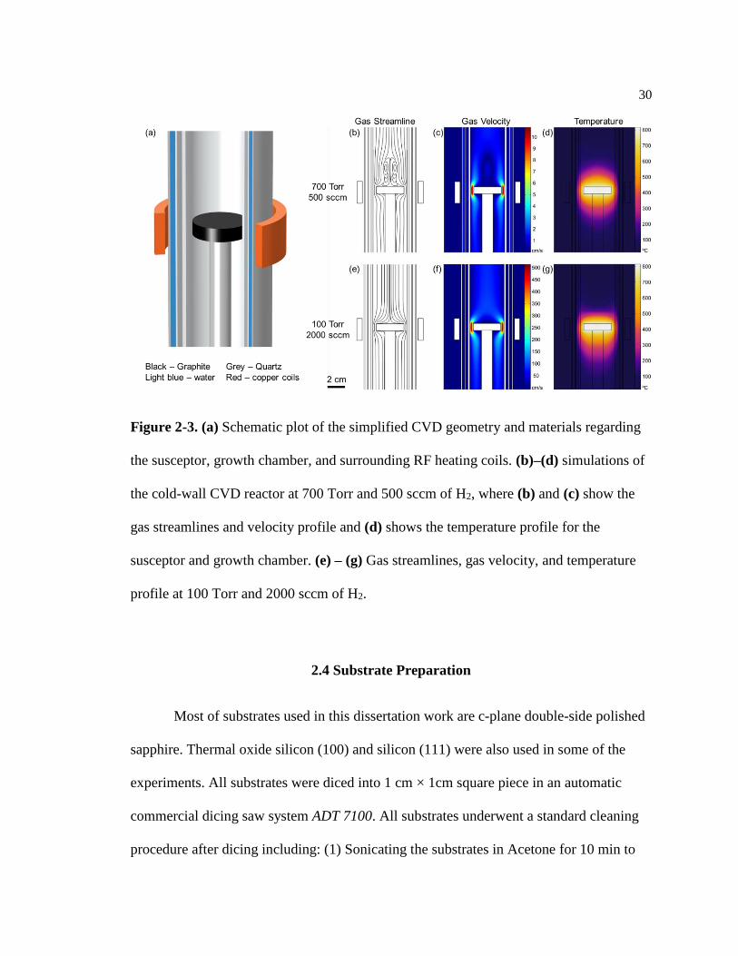
30
Figure 2-3. (a) Schematic plot of the simplified CVD geometry and materials regarding
the susceptor, growth chamber, and surrounding RF heating coils. (b)–(d) simulations of
the cold-wall CVD reactor at 700 Torr and 500 sccm of H2, where (b) and (c) show the
gas streamlines and velocity profile and (d) shows the temperature profile for the
susceptor and growth chamber. (e) – (g) Gas streamlines, gas velocity, and temperature
profile at 100 Torr and 2000 sccm of H2.
2.4 Substrate Preparation
Most of substrates used in this dissertation work are c-plane double-side polished
sapphire. Thermal oxide silicon (100) and silicon (111) were also used in some of the
experiments. All substrates were diced into 1 cm × 1cm square piece in an automatic
commercial dicing saw system ADT 7100. All substrates underwent a standard cleaning
procedure after dicing including: (1) Sonicating the substrates in Acetone for 10 min to

31
dissolve most of contamination; (2) Sonicating the substrates in Isopropyl alcohol for 10
min to remove Acetone; (3) Rinsing the substrates with deionized water for 5 times to
remove Isopropyl alcohol; (4) Drying the substrates with high-pressure nitrogen gun; (5)
immersing the substrates into commercial Piranha solution (Nano-Strip, KMG Electronic
Chemicals) under 85-100 for 20 minutes to get rid of any stubborn residue; (6) rinsing the
substrates again with deionized water for 5 times to remove the Piranha solution; (7)
Drying the substrates with high-pressure nitrogen gun and placing them into containers.
To remove the native oxide layer on silicon (111) substrate, additional treatment
was applied after the standard cleaning procedure: (1) Immersing the substrates into 10%
diluted hydrogen fluoride solution for 10 minutes to remove all the native oxide; (2)
Rinsing the substrates again with deionized water for 5 times to remove the hydrogen
fluoride solution; (3) Drying the substrates with high-pressure nitrogen gun and placing
them into containers. Note that hydrogen fluoride solution is not compatible with glass
beakers so Teflon beakers were used in this process. The silicon (111) substrate surface
should be terminated with H and F and the substrate was rapidly placed into the growth
reactor in case of any further oxidation.
2.5 Etch-free Transfer of 2D TMD films
Current study and development of 2D materials including heterostructure, device
fabrication, and characterization require an easy and clean way to transfer the films onto
arbitrary substrates. The etch-free transfer method presented in this section (designed by
Fu Zhang, Penn State) introduce a simple and etchant free process to transfer wafer-scale

32
monolayer films from sapphire to other substrates only involving PMMA and H2O.
Instead of deep etching of the sample in hot base solutions, such as HF and KOH,6–8 the
PMMA-coated film can be directly delaminated and separated from sapphire substrate
by simply dipping the sample in water. The process also helps to keeps the film in its
pristine structure and free from degradation of the crystal due to ultrasonication9 or
exposure to chemicals from pre-etching in NaOH or other strong solutions.10
The transfer process is schematically illustrated in Figure 2-4 with five main
steps: (1) PMMA is first spin-coated on the substrate with the nanostructures and the
assembly is kept at room temperature overnight (Figure 2-4a and 2-4b); (2) Using blade,
small gaps are created along the edge contours of the sapphire substrate (Figure 2-4c); (3)
The assembly is immersed in hot water (~80 ℃) for 5-10 minutes. Due to the
hydrophobic nature of the 2D materials (such as graphene11 and TMDs12) and PMMA
compared with the hydrophilic character of the sapphire substrate,13,14 the water can
easily penetrate to the interface from the created gap due to the capillary forces and
further lift off the PMMA/film from the sapphire substrate while in water (Figure 2-4d).
In this step, both the substrate feeding angle (~ 45°) with respect to the water surface and
delamination rate (~ 1mm/s) need to be controlled to minimize the mechanical force and
damage and to maintain the integrity of the transferred film. Since no chemical etchants
are used in this process, sapphire substrate remains intact and can be reused for further
growth. (4) The detached PMMA/film assembly can further be picked up from water with
any other target substrate and placed on the hot plate (~70 ℃) for 10 minutes to improve
the film/substrate attachment. (5) PMMA is removed with acetone and IPA/methanol to

33
further eliminate any remaining organic residuals. This PMMA-assisted water transfer
method significantly reduces the possible damage and chemical attacks during the
transfer process. In addition, since no chemical etchants are involved in the process,
PMMA/nanostructure assembly can be directly picked up by any water-compatible
substrate. All the film transfers mentioned in this dissertation adopted this method.
Figure 2-4. The schematic illustration of the etchant-free transfer method. (a) A 2D
material film is grown on sapphire; (b) PMMA is Spin-coated on the film; (c) the film is
scratched along the edge contours of the sapphire substrate using a blade; (d) The whole
assembly is immersed into hot water (~80 ℃) by a feeding angle ~ 45° for 5 to 10
minutes before the hydrophobic PMMA/2D film is delaminated from the sapphire
substrate and floats on the water surface.

34
2.6 Characterization Techniques of 2D TMD films
2.6.1 Atomic force microscopy
Atomic Force Microscopy (AFM) is known as one of the techniques to capture
topographic morphology of sample surfaces. Nowadays, the latest AFM can achieve
atomic resolution in the z-direction while maintain swift scanning rate in the xy-plane.
This provides the opportunity to identify the variation of monoatomic step height on the
sample surface over a micron-level area, which matches perfectly with the requirement of
characterizing the morphology of 2D materials with only a few-atom thickness in z-
direction. In addition, AFM also allows atomic resolution in xy-plane which offers
additional ways to identify surface defects and moiré pattern between monolayer
materials and substrates. In addition to traditional contact (Figure 2-5a) and tapping
modes (Figure 2-5b), novel modes such as PeakForce Tapping mode in Figure 2-5c
(which is used in this dissertation work) have been developed to stably control ultralow
imaging force to preserve both the AFM tip and fragile samples.15 This allows AFM
acquiring information of surface for modulus, adhesion, deformation, conductivity,
surface potential, and so on in addition to the topography and local force knowledge from
conventional modes. Therefore, modern AFM can also allow studies for mechanical,
electrical, and piezoelectrical properties. While AFM tip does get in contact with sample
surface during the scan (in PeakForce Tapping mode), the weak force between tip and
surface (typical around piconewton to nanonewton) can limit the damage on sample to
minimal. On the other hand, AFM can work under variant unaggressive environments
including liquid, varied temperature, glove box, and vacuum, which enable

35
multidisciplinary research on 2D materials such as studying black phosphorus in the inert
gas glove box where oxidation can be significant reduced. Therefore, AFM stands out as
one of the most common characterization techniques for 2D materials.
Figure 2-5. Schematic representation of basic AFM modes: (a) Contact mode with tip-
sample force as a feedback setpoint (𝐹sp); (b) Tapping or AC mode where the setpoint is
oscillation amplitude (𝐴sp) or frequency (𝑓sp); (c) PeakForce Tapping mode where the
tip is modulated at an off-resonance frequency and the feedback setpoint is the maximum
force, or peak force, of each tapping cycle.15

36
2.6.2 Raman and photoluminescence spectroscopy
Raman spectroscopy provides a quick and nondestructive method for
characterizing the 2D materials.16–18 Typical measurements can be made at varied
temperature from 4K to elevated temperature and pressure from vacuum to high pressure
without complicated sample preparation processes. Raman scattering involves the
inelastic scattering of the incident light in a material, where the energy of the scattered
light either decreases by exciting an elementary excitation of a phonon or increases by
absorbing a phonon. Raman spectra give the intensity of the scattered light as a function
of the energy shift from the incident light which is called as Raman shift. Since the
discovery of graphene and development of other atomic layer materials including TMDs,
Raman spectroscopy has rapidly become a standard characterization technique for the
characterization of low dimensional materials due to several advantages. The strong
interaction between incident photon and phonon from the layer gives clear characteristic
phonon frequency peaks in Raman spectra even down to monolayer level. The sensitive
photon-phonon interaction can not only distinguish the materials but also obtain
additional information including strain, doping level, alloy component, etc. In addition,
by focusing the laser light in a confocal optical microscope, we can measure a high
spatially resolved Raman signal within a few hundred nanometers. Therefore, Raman
maps can also be achieved by scanning the focused laser light across the sample surface,
in which information regarding the distribution of strain, defects, doping, and so on can
be told over a relatively large area.

37
Photoluminescence (PL) spectroscopy describes the radiative emission of
materials after excitation of photons. Similar to Raman spectroscopy, it is also a
nondestructive characterization technique and in many cases it can be done in the same
instrumental system of Raman spectroscopy (as long as the laser and spectrometer
provides the suitable energy range). Unlike the Raman spectroscopy which measure the
inelastic Raman shift from incident light, PL response comes from the direction emission
from conduction band to valence band of material and is intrinsic to material itself and
therefore has no correlation with incident laser light. PL also becomes a standard and
significant technique for 2D materials, especially TMDs, due to their unique PL emission
and potential optical and optoelectronic applications. Typical monolayer TMDs have
direct band gap and thus have strong PL emission.19,20 While in additional to this.
Monolayer TMDs often show strong exciton binding energy because of the strong
Coulomb interaction between the electrons and holes due to the quantum confinement
effect, 19–21 which makes the PL emission peak away from the direct bandgap energy
(typically a few hundred meV). Moreoever, there are other quasiparticles in the
monolayer TMDs such as trion that raise a lot of interest. A trion can be formed by
exciton-electron pair under high carrier density, however, they are unstable and rarely
observed in conventional semiconductors.22,23 In comparison, trions are reported stable in
monolayer TMDs,24,25 and can be controlled by optical, electronic26,27 or chemical28
methods. In this way, the emission of trions can be modified intentionally in monolayer
TMDs for potential tunable photonic devices.

38
2.6.3 In-plane X-ray diffraction
For the determination of the epitaxial relation in classical thin films, the technique
of choice is X-ray diffraction (XRD) pole figure measurements. This technique is also
nondestructive and usually does not require sample preparation and is fast. In this
technique, an {hkl} plane family with h and/or k and l not equal to zero is probed for both
film and substrate to determine crystallographic orientation. However, 2D monolayers
and few-layer films that is often assumed to be impossible for conventional XRD due to
the lack of periodicity in the third dimension. While there is no crystal periodicity out-of-
plane, the in-plane component is present and has been probed by implementing XRD θ-
2θ and ϕ measurements in the in-plane geometry, to observe the presence of the
reciprocal space points and their distribution, respectively. Thus, for the transition metal
dichalcogenides where both constituents have high electron density, lab scale X-ray
diffraction performed with the X-ray incidence plane nearly coinciding with the sample
surface plane (an offset angle that is higher than the X-ray total external reflection angle)
should be able to determine the in-plane epitaxial relation between the film and the
substrate. “Nearly” in this case is determined by the X-ray total external reflection angle
which is materials dependent and usually below 1° from the surface to the beam. This
technique is so-called in-plane XRD since it can determine the in-plane epitaxial relation
between films and substrates. It can also tell presence of different crystal phases as well
as alloy formation and its composition similar to conventional XRD.
Figure 2-6 shows illustrations of the Bragg-Brentano measurement geometry
(Figure 2-6a) where the X-ray scattering vector Q (Q= k1-k0) is normal to the sample

39
surface (parallel to surface normal n) and in-plane measurement geometry illustrations
from two sides (Figure 2-6b and 2-6c).29 In this illustration, k0 and k1 are the incident and
diffracted beams, respectively. Angle ω is an angle between incident beam k0 and a
vector that defines the intersection line between the sample surface and the X-ray
incidence planes. In Bragg-Brentano geometry, this angle is well defined while in in-
plane diffraction this angle coincides with the angle ϕ that defines the rotation of the
sample around its surface normal n. Angle χ is defined as an angle between the surface
normal n and the X-ray incidence plane. 2θ angle is an angle between incident k0 and
diffracted k1 beams.
Figure 2-6. (a) Bragg-Brentano measurement geometry. (b) and (c) In-plane
measurement geometry from two perspectives.(Mikhail Chubarov, Penn State)29
2.6.4 Transmission electron microscopy
Characterization of atomic and chemical structure of materials is the key to
understand the physic and chemistry properties at nanoscale and to further tune the
properties.30 The nature of the atomic bonding structure gives direct information
regarding both electronic and mechanical properties. The nanoscale structure change

40
(such as defects, substitutional doping, grain boundary) in 2D materials can be even more
crucial considering they have limited expansion in z-direction. In order to achieve high
spatial resolution studies, aberration-corrected high-resolution transmission electron
microscopy (AC-HRTEM) and scanning transmission electron microscopy (S/TEM) are
commonly used for 2D materials. The atomically thin and transferrable properties of 2D
materials advance the imaging the materials under TEM as film/flake can be suspended
on the TEM grid easily. In addition, large area imaging and diffraction can be performed
to gain information regarding the crystallinity of the films and moiré pattern of stacking
and twisted stacking 2D materials can also be identified and studied under TEM, which
has been recently reported to probe new physic properties.31–33
Additionally, several advances have been critical in the field of electron
microscopy which have allowed for atomic resolution imaging of 2D materials. Hardware
aberration corrector electron optics dramatically minimizes the effect of intrinsic
spherical aberrations of electron lenses and chromatic aberration correctors or
monochromators can reduce the energy spread of the electron beam illumination for sub-
ångstrom imaging.34 The other important perspective is the low accelerating voltages
(~60-80 kV) has been developed for imaging of 2D materials. The dramatically reduces
the possible damage to the sample as well as the increasing electron scattering cross-
section at low voltage, which produces more contract for a given illumination dose.35,36

41
2.7 References
(1) Ohring, M. Materials Science of Thin Films : Deposition and Structure;
Academic Press, 2002.
(2) Lai, K. K.; Lamb, H. H. Tungsten Chemical Vapor Deposition Using Tungsten
Hexacarbonyl: Microstructure of as-Deposited and Annealed Films. Thin Solid Films
2000, 370 (1), 114–121.
(3) Lander, J. J.; Germer, L. H. Plating Molybdenum, Tungsten, and Chromium by
Thermal Decomposition of Their Carbonyls. Trans. Am. Inst. Min. Metall. Eng. 1948,
175, 648–692.
(4) Karlson, U.; Frankenberger, W. T.; Spencer, W. F. Physicochemical Properties of
Dimethyl Selenide and Dimethyl Diselenide. J. Chem. Eng. Data 1994, 39 (3), 608–610.
(5) Shenai-Khatkhate, D. V.; DiCarlo, R. L.; Ware, R. A. Accurate Vapor Pressure
Equation for Trimethylindium in OMVPE. J. Cryst. Growth 2008, 310 (7–9), 2395–2398.
(6) Zhang, Y.; Zhang, Y.; Ji, Q.; Ju, J.; Yuan, H.; Shi, J.; Gao, T.; Ma, D.; Liu, M.;
Chen, Y.; Song, X.; Hwang, H. Y.; Cui, Y.; Liu, Z. Controlled Growth of High-Quality
Monolayer WS2 Layers on Sapphire and Imaging Its Grain Boundary. ACS Nano 2013, 7
(10), 8963–8971.
(7) Lin, Y.-C.; Zhang, W.; Huang, J.-K.; Liu, K.-K.; Lee, Y.-H.; Liang, C.-T.; Chu,
C.-W.; Li, L.-J. Wafer-Scale MoS2 Thin Layers Prepared by MoO3 Sulfurization.
Nanoscale 2012, 4 (20), 6637.
(8) Elías, A. L.; Perea-López, N.; Castro-Beltrán, A.; Berkdemir, A.; Lv, R.; Feng, S.;

42
Long, A. D.; Hayashi, T.; Kim, Y. A.; Endo, M.; Gutiérrez, H. R.; Pradhan, N. R.;
Balicas, L.; Mallouk, T. E.; López-Urías, F.; Terrones, H.; Terrones, M. Controlled
Synthesis and Transfer of Large-Area WS2 Sheets: From Single Layer to Few Layers.
ACS Nano 2013, 7 (6), 5235–5242.
(9) Ma, D.; Shi, J.; Ji, Q.; Chen, K.; Yin, J.; Lin, Y.; Zhang, Y.; Liu, M.; Feng, Q.;
Song, X.; Guo, X.; Zhang, J.; Zhang, Y.; Liu, Z. A Universal Etching-Free Transfer of
MoS2 Films for Applications in Photodetectors. Nano Res. 2015, 8 (11), 3662–3672.
(10) Xu, Z.-Q.; Zhang, Y.; Lin, S.; Zheng, C.; Zhong, Y. L.; Xia, X.; Li, Z.; Sophia, P.
J.; Fuhrer, M. S.; Cheng, Y.-B.; Bao, Q. Synthesis and Transfer of Large-Area Monolayer
WS2 Crystals: Moving Toward the Recyclable Use of Sapphire Substrates. ACS Nano
2015, 9 (6), 6178–6187.
(11) Qi, J. L.; Wang, X.; Lin, J. H.; Zhang, F.; Feng, J. C.; Fei, W.-D. A High-
Performance Supercapacitor of Vertically-Oriented Few-Layered Graphene with High-
Density Defects. Nanoscale 2015, 7 (8), 3675–3682.
(12) Chow, P. K.; Singh, E.; Viana, B. C.; Gao, J.; Luo, J.; Li, J.; Lin, Z.; Elías, A. L.;
Shi, Y.; Wang, Z.; Terrones, M.; Koratkar, N. Wetting of Mono and Few-Layered WS2
and MoS2 Films Supported on Si/SiO2 Substrates. ACS Nano 2015, 9 (3), 3023–3031.
(13) Azimi, G.; Dhiman, R.; Kwon, H.-M.; Paxson, A. T.; Varanasi, K. K.
Hydrophobicity of Rare-Earth Oxide Ceramics. Nat. Mater. 2013, 12 (4), 315–320.
(14) Gurarslan, A.; Yu, Y.; Su, L.; Yu, Y.; Suarez, F.; Yao, S.; Zhu, Y.; Ozturk, M.;
Zhang, Y.; Cao, L. Surface-Energy-Assisted Perfect Transfer of Centimeter-Scale

43
Monolayer and Few-Layer MoS 2 Films onto Arbitrary Substrates. ACS Nano 2014, 8
(11), 11522–11528.
(15) Zhang, H.; Huang, J.; Wang, Y.; Liu, R.; Huai, X.; Jiang, J.; Anfuso, C. Atomic
Force Microscopy for Two-Dimensional Materials: A Tutorial Review. Opt. Commun.
2018, 406, 3–17.
(16) Dresselhaus, M. S.; Jorio, A.; Saito, R. Characterizing Graphene, Graphite, and
Carbon Nanotubes by Raman Spectroscopy. Annu. Rev. Condens. Matter Phys. 2010, 1
(1), 89–108.
(17) Saito, R.; Hofmann, M.; Dresselhaus, G.; Jorio, A.; Dresselhaus, M. S. Raman
Spectroscopy of Graphene and Carbon Nanotubes. Adv. Phys. 2011, 60 (3), 413–550.
(18) Zhang, X.; Qiao, X.-F.; Shi, W.; Wu, J.-B.; Jiang, D.-S.; Tan, P.-H. Phonon and
Raman Scattering of Two-Dimensional Transition Metal Dichalcogenides from
Monolayer, Multilayer to Bulk Material. Chem. Soc. Rev. 2015, 44 (9), 2757–2785.
(19) Cheiwchanchamnangij, T.; Lambrecht, W. R. L. Quasiparticle Band Structure
Calculation of Monolayer, Bilayer, and Bulk MoS2. Phys. Rev. B 2012, 85 (20), 205302.
(20) Mak, K. F.; Lee, C.; Hone, J.; Shan, J.; Heinz, T. F. Atomically Thin MoS2: A
New Direct-Gap Semiconductor. Phys. Rev. Lett. 2010, 105 (13), 136805.
(21) Li, T.; Galli, G. Electronic Properties of MoS2 Nanoparticles. J. Phys. Chem. C
2007, 111 (44), 16192–16196.
(22) Tripathi, G. S. Itinerant Electrons in Strong Magnetic Fields: Onset of a
Metamagnetic Transition. Phys. Rev. B 1995, 52 (9), 6522–6529.

44
(23) Finkelstein, G.; Shtrikman, H.; Bar-Joseph, I. Optical Spectroscopy of a Two-
Dimensional Electron Gas near the Metal-Insulator Transition. Phys. Rev. Lett. 1995, 74
(6), 976–979.
(24) Stébé, B.; Ainane, A. Ground State Energy and Optical Absorption of Excitonic
Trions in Two Dimensional Semiconductors. Superlattices Microstruct. 1989, 5 (4), 545–
548.
(25) Tongay, S.; Zhou, J.; Ataca, C.; Liu, J.; Kang, J. S.; Matthews, T. S.; You, L.; Li,
J.; Grossman, J. C.; Wu, J. Broad-Range Modulation of Light Emission in Two-
Dimensional Semiconductors by Molecular Physisorption Gating. Nano Lett. 2013, 13
(6), 2831–2836.
(26) Mak, K. F.; He, K.; Lee, C.; Lee, G. H.; Hone, J.; Heinz, T. F.; Shan, J. Tightly
Bound Trions in Monolayer MoS2. Nat. Mater. 2013, 12 (3), 207–211.
(27) Ross, J. S.; Wu, S.; Yu, H.; Ghimire, N. J.; Jones, A. M.; Aivazian, G.; Yan, J.;
Mandrus, D. G.; Xiao, D.; Yao, W.; Xu, X. Electrical Control of Neutral and Charged
Excitons in a Monolayer Semiconductor. Nat. Commun. 2013, 4 (1), 1474.
(28) Mouri, S.; Miyauchi, Y.; Matsuda, K. Tunable Photoluminescence of Monolayer
MoS2 via Chemical Doping. Nano Lett. 2013, 13 (12), 5944–5948.
(29) Chubarov, M.; Choudhury, T. H.; Zhang, X.; Redwing, J. M. In-Plane x-Ray
Diffraction for Characterization of Monolayer and Few-Layer Transition Metal
Dichalcogenide Films. Nanotechnology 2018, 29 (5), 055706.
(30) Rasool, H. I.; Ophus, C.; Zettl, A. Atomic Defects in Two Dimensional Materials.

45
Adv. Mater. 2015, 27 (38), 5771–5777.
(31) Cao, Y.; Fatemi, V.; Demir, A.; Fang, S.; Tomarken, S. L.; Luo, J. Y.; Sanchez-
Yamagishi, J. D.; Watanabe, K.; Taniguchi, T.; Kaxiras, E.; Ashoori, R. C.; Jarillo-
Herrero, P. Correlated Insulator Behaviour at Half-Filling in Magic-Angle Graphene
Superlattices. Nature 2018, 556 (7699), 80–84.
(32) Cao, Y.; Fatemi, V.; Fang, S.; Watanabe, K.; Taniguchi, T.; Kaxiras, E.; Jarillo-
Herrero, P. Unconventional Superconductivity in Magic-Angle Graphene Superlattices.
Nature 2018, 556 (7699), 43–50.
(33) Yoo, H.; Engelke, R.; Carr, S.; Fang, S.; Zhang, K.; Cazeaux, P.; Sung, S. H.;
Hovden, R.; Tsen, A. W.; Taniguchi, T.; Watanabe, K.; Yi, G.-C.; Kim, M.; Luskin, M.;
Tadmor, E. B.; Kaxiras, E.; Kim, P. Atomic and Electronic Reconstruction at the van Der
Waals Interface in Twisted Bilayer Graphene. Nat. Mater. 2019, 18 (5), 448–453.
(34) Warner, J. H.; Margine, E. R.; Mukai, M.; Robertson, A. W.; Giustino, F.;
Kirkland, A. I. Dislocation-Driven Deformations in Graphene. Science. 2012, 337 (6091),
209–212.
(35) Suenaga, K.; Koshino, M. Atom-by-Atom Spectroscopy at Graphene Edge.
Nature 2010, 468 (7327), 1088–1090.
(36) Urban, K. W.; Meyer, J. C.; Erni, R.; Rossell, M. D.; Kisielowski, C.; Yang, L.;
Park, C.-H.; Crommie, M. F.; Cohen, M. L.; Louie, S. G.; Zettl, A. Studying Atomic
Structures by Aberration-Corrected Transmission Electron Microscopy. Science. 2008,
321 (5888), 506–510.

46
Chapter 3
Influence of Carbon and Precursor Consideration in the Growth of
WSe2
This chapter discusses initial development of a metalorganic chemical vapor
deposition (MOCVD) of monolayer or few-layer WSe2 thin films and the influence of
unintentional carbon incorporation when using metalorganic chalcogen precursor. The
results demonstrate the presence of a defective graphene layer that forms simultaneously
during MOCVD growth of WSe2 on sapphire at high growth temperature and high Se:W
ratio when using dimethyl selenide as chalcogen precursors. The formation of the
defective graphene layer on sapphire competes with the nucleation and lateral growth of
WSe2 ultimately suppressing lateral growth and increasing the vertical growth rate of the
domains. The alternative use of hydride chalcogen precursor such as hydrogen selenide
eliminates the main carbon source during the growth process and thus prevents the
formation of defective graphene layer enables coalesced monolayer and few-layer WSe2
films.
3.1 Introduction
Unintentional carbon incorporation has been a persistent problem in metalorganic
chemical vapor deposition (MOCVD) processes due to the use of precursor molecules
with organic ligands. In the conventional MOCVD growth of III-V compound
semiconductor thin films, carbon concentrations are typically lower than 1015 cm-3.1
However, even low levels of carbon can impact device performance and therefore carbon

47
as both an unintentional impurity and intentional dopant in MOCVD has been thoroughly
investigated over the years. Compared to conventional MOCVD-grown semiconductor
layers which may be hundreds of nanometers or more in thickness, two-dimensional (2D)
transition metal dichalcogenide (TMD) monolayers are atomically thin with highly
reactive edge surfaces and are bound to the substrate by van der Waals forces. Therefore,
the presence of even small amounts of carbon in TMD growth may impact the nucleation
and lateral growth of TMD layers and the resulting structural, optical and electrical
properties of the films.
In the case of WSe2, previous studies have demonstrated that MOCVD growth
conditions, particularly substrate temperature and selenium-to-tungsten (Se:W) ratio, play
a significant role in the nucleation and lateral growth of the films.2 The high melting
temperature/low vapor pressure of transition metals such as W in this case results in
reduced surface adatom mobility which necessitates the use of high substrate
temperatures (>600 oC) to enhance surface diffusion and achieve large domain sizes. On
the other hand, the low melting temperature/high vapor pressure of Se and other
chalcogens reduces the sticking coefficient of Se on the growth surface which makes it
necessary to use very high Se:W ratios in order to achieve large and stoichiometric
domains.2 While high Se:W can be obtained using metalorganic precursors through
manipulating the bubbler temperatures for intentional vapor pressure and controlling the
carrier gas through the bubblers, the extreme high flow rate of metalorganic precursor
and high growth temperature raises the concern of carbon contamination. Although the
presence of residual carbon was noted in TMD monolayer and few-layer thin films grown

48
using MOCVD precursors,2,3 the reason for the formation of the carbon in the films has
not been understood and the influence of the carbon has not been investigated in detail.
In this chapter, we examined the growth of WSe2 thin films on (0001) sapphire
(α-Al2O3) substrates by MOCVD in a vertical cold-wall reactor chamber using tungsten
hexacarbonyl (W(CO)6), dimethyl selenide (DMSe) and hydrogen selenide (H2Se) as
precursors. The results reveal the formation of a defective graphene layer on the sapphire
substrate at high substrate temperature (~800 oC) and Se/W ratios over 3200 when DMSe
is used as the Se precursor which competes with the nucleation and growth of WSe2 on
the sapphire surface and impacts the lateral growth as well as the epitaxy of the triangular
WSe2 islands. In comparison, carbon contamination does not occur when H2Se is used in
place of DMSe indicating that the methyl radicals from DMSe are the primary source of
carbon. Without the competition from carbon contamination, a high nucleation rate and a
coalesced WSe2 film can be achieved when selecting H2Se as chalcogen precursor. These
results identify the influence of carbon in the MOCVD growth of 2D TMD films and
suggest a carbon-free hydride chalcogen as a better choice in precursor selection, which
establish the foundation of further study in Chapter 4 and 5.
3.2 Experimental Details
3.2.1 MOCVD growth conditions
Tungsten diselenide films were synthesized using W(CO)6 (Sigma-Aldrich,
99.99% purity), DMSe (NOVA-KEM, 99.99% purity) and H2Se (Matheson, 99.998%

49
purity) in the cold-wall vertical quartz tube reactor with an inductively heated SiC-coated
graphite susceptor. Ultra high purity hydrogen was used as the carrier gas through the
bubblers and reactor to maintain a total flow rate at 450 sccm. The W(CO)6 powder was
contained inside a stainless steel bubbler which was held at 30 oC and 730 Torr.
Hydrogen carrier gas was passed through the bubbler at a flow rate of 15 sccm which
resulted in a W(CO)6 flow rate of 9×10⁻⁴ sccm out of the bubbler. DMSe liquid was also
contained inside a stainless steel bubbler which was held at room temperature and 760
Torr. Hydrogen carrier gas was passed through the bubbler at a flow rate in the range of
2.5-25 sccm which resulted in a DMSe flow rate of 0.75-7.5 sccm out of the bubbler.
Growth was carried out at a total reactor pressure of 700 Torr, a growth time of 30 min
and a substrate temperature of 800 oC for all experiments. As-received c-plane (0001)
double-side polished sapphire were used as substrates.
3.2.2 Post-growth characterization setup
To analyze the composition of the atomically thin films, surface elemental
compositions of different regions on the sample were analyzed by high resolution Auger
electron spectroscopy (AES) in a PHI 720 Scanning Auger Nanoprobe using 10keV
electron beam energy. Raman spectroscopy was carried out in a HORIBA LabRAM HR
Evolution high spectral resolution analytical Raman microscope with a laser wavelength
of 532 nm. To measure the film thickness and domain heights, a step edge was formed on
the as-grown WSe2 film via using a plastic tweezer to scratch the sample surface and the
step height was profiled using a Digital Instruments Multimode Atomic Force

50
Microscope (AFM). Compared the AFM, larger range of surface morphology of the
samples were shown in field emission scanning electron microscopy (FESEM) images
obtained in a Zeiss Merlin instrument. Transmission electron microscopy (TEM) was
used to examine the cross-sectional morphology and obtain structural information on the
WSe2 samples. Cross-sectional TEM samples were fabricated by the focused ion beam
(FIB) method on a HELIOS Nanolab 660. A thin layer of gold was sputtered on top of
the substrate to enhance the conductivity and a layer of platinum was deposited to protect
and mark the cut region. A FEI Tecnai G2 TEM operating at 80 kV was used to study the
atomic structure of the WSe2 samples produced in this study.
3.3 Chalcogen Precursor: DMSe
3.3.1 Effect of Se:W ratio and high DMSe flow rate
The effect of Se:W ratio on the nucleation and lateral growth of WSe2 on sapphire
was initially investigated by maintaining a constant W(CO)6 partial pressure of 1.4×10⁻³
Torr in the reactor chamber and varying the flow rate of DMSe to change the Se:W ratio
from approximately 800 to 8000. The WSe2 domain size increased and the nucleation
density decreased as the Se:W ratio was increased from 800 to 4800 as shown in Figure
3-1. This follows the expectation as the increased Se:W ratio results in the surface species
moving towards to stoichiometric ratio due to the large vapor pressure difference between
Se and W. Therefore the growth rate of domains increases and the nucleation density
decreases in compensation for surface species participating into the growth of existing

51
domains. In addition, AFM results in Figure 3-2 shows the domain thickness increases
with increasing Se:W ratio. This indicates the surface energy changed on the substrates
since the WSe2 domains prefer to wet the whole sapphire surface at low Se:W ratio while
they prefer to stay on top of themselves at high Se:W ratio.
Further increases in the Se:W ratio up to 8000 did not result in a significant increase in
the domain size or a reduction in both nucleation density and surface coverage as shown
in Figure 3-3a and 3-3b. Interestingly, while the surface coverage of WSe2 domains was
reduced at high Se:W ratios above 3200, the height of the domains increased significantly
from < 10 nm at Se:W=3200 to 20-30 nm for Se:W ratios ranging from 4800 to 8000
Figure 3-2. AFM images of WSe2 domains grown on sapphire substrate using DMSe
and W(CO)6 as precursors with Se:W ratios of (a) 800, (b) 1600, (c) 3200, (d) 4800.
Figure 3-1. FESEM images of WSe2 domains grown on sapphire substrate using DMSe
and W(CO)6 as precursors with Se:W ratios of (a) 800, (b) 1600, (c) 3200, (d) 4800.
The (e) average domain size, (f) surface coverage and (g) domain thickness of the as-
grown WSe2 at Se:W ratios from 800 to 8000.

52
(Figure 3-3c). In addition, as the Se:W ratio was increased above 3200, the edges of the
triangular domains become jagged and pits appear in the islands and near the domain
edges (Figure 3-1d). Prior studies have reported changes in the shape and edge structure
of TMD domains as a function of the chalcogen-to-metal ratio4 and growth rate5 and in
the presence of impurities and oxidation6 and intentional dopants7.
Figure 3-3. The (a) average domain size, (b) surface coverage and (c) domain thickness
of the as-grown WSe2 at Se:W ratios from 800 to 8000.

53
3.3.2 Discovery of defective graphene layer
The change in the lateral versus vertical growth rate at high Se:W ratios as well as
the deformed edge shape in the previous section suggests changes in surface energy
which make it more energetically favorable for the WSe2 to grow vertically on existing
domains instead of laterally on the substrate surface. When examining the scratched
sample surface that was used to obtain a step height for domain thickness measurements
by FESEM (Figure 3-4a), a region of darker contrast (region 3) was observed between
the WSe2 triangle domains (region 2) and the sapphire surface (region 1) at the scratched
boundary, which suggested the presence of a thin layer of different conductivity on the
surface. This layer was determined to be ~1.5 nm thick from AFM measurements in the
scanned region (Figure 3-4b). The combining FESEM and AFM results confirm an
additional coalesced layer formed between WSe2 domains and sapphire substrate surface
during the growth. In order to identify the composition of this layer, AES was used to
analyze the elemental composition of the three regions with different FESEM contrasts,
and the results are shown in Figure 3-4c (done by Zakaria Al Balushi, Penn State). Note
that AES is merely sensitive to compositional surface element and thus should not be
affected by the impurity in the deep of sapphire substrates. Only Al and O were detected
on the sapphire surface region (region 1). As expected, W and Se elements were detected
in the triangular domain regions (region 2) consistent with the formation of WSe2 along
with a small carbon signal. In the region between the WSe2 domains (region 3), however,
a strong carbon signal was observed but no W or Se signals indicating that the thin layer
on the sapphire surface contains mostly carbon.

54
Now that the additional layer was identified as carbon layer, cross-sectional TEM
was applied to acquire further structural information of this carbon layer (done by Fu
Zhang, Penn State). A cross-sectional TEM image of the sample grown using DMSe at
Figure 3-4. (a) FESEM image of the WSe2 sample grown at 800 oC with Se:W=3200
showing three regions: 1) sapphire surface; 2) WSe2 triangular domains; 3) region of
darker contrast between WSe2 islands. (b) AFM image revealing a continuous layer
~1.5 nm thick and WSe2 triangular domains ~6-9 nm thick on the sapphire surface. (c)
AES spectra indicating the presence of Al and O in region 1, W, Se and C in region 2,
and Al, O, and C in region 3.

55
800 oC and Se:W=3200, shown in Figure 3-5, obtained in an area similar to that of region
2 above, revealed a carbon layer beneath the WSe2 domains. The thickness of this carbon
layer is ~2 nm, which is consistent with the AFM thickness measurement in Figure 3-4b.
Additional cross-sectional TEM images obtained from different regions across the sample
in Figure 3-6 show that the thickness of the carbon layer varies from ~1.2 to ~5.5 nm.
The WSe2 layer is ~6 nm thick and shows a layered structure with spacing between layers
of ~0.67 nm which is consistent with WSe2. Some regions of the carbon layer exhibit a
layered structure indicating the formation of graphene.
Figure 3-5. Cross-sectional TEM image of WSe2 sample grown using DMSe at 800
oC and Se:W=3200 revealing a carbon layer beneath the WSe2. Some regions of the
carbon layer exhibit a layered structure typical of defective graphene.

56
3.3.3 Origin of defective graphene layer
The carbon layer present in the WSe2 sample shown in Figures 2 and 3 likely
results from the high concentration of carbon-containing ligands present in the MOCVD
growth environment. Prior studies have demonstrated that methane (CH4) can be used as
a precursor to deposit graphene on sapphire at temperatures as low as 950oC.8,9 Graphene
produced by this process is typically defective as demonstrated by the presence of a
strong D peak at ~1350 cm-1 in the Raman spectra.8,10,11 The methyl radicals produced by
the decomposition of the DMSe precursor are likely responsible for the formation of the
carbon layer on sapphire in the WSe2 MOCVD process. Methyl radicals (CH3*) are more
chemically reactive than CH4, consequently, this could lead to defective graphene
formation at the lower temperatures (800oC) used in this study. Furthermore, the high
Se:W ratios utilized in the growth result in an inlet C:W ratio which is two times higher
than the Se:W ratio creating a carbon-rich growth environment. To investigate this
Figure 3-6. Cross-sectional TEM images of different regions on the WSe2 sample
grown using DMSe at 800 oC and Se:W=3200 showing different carbon layer
thickness (a) ~1.2nm; (b) ~2.7nm; (c) ~5.5nm.
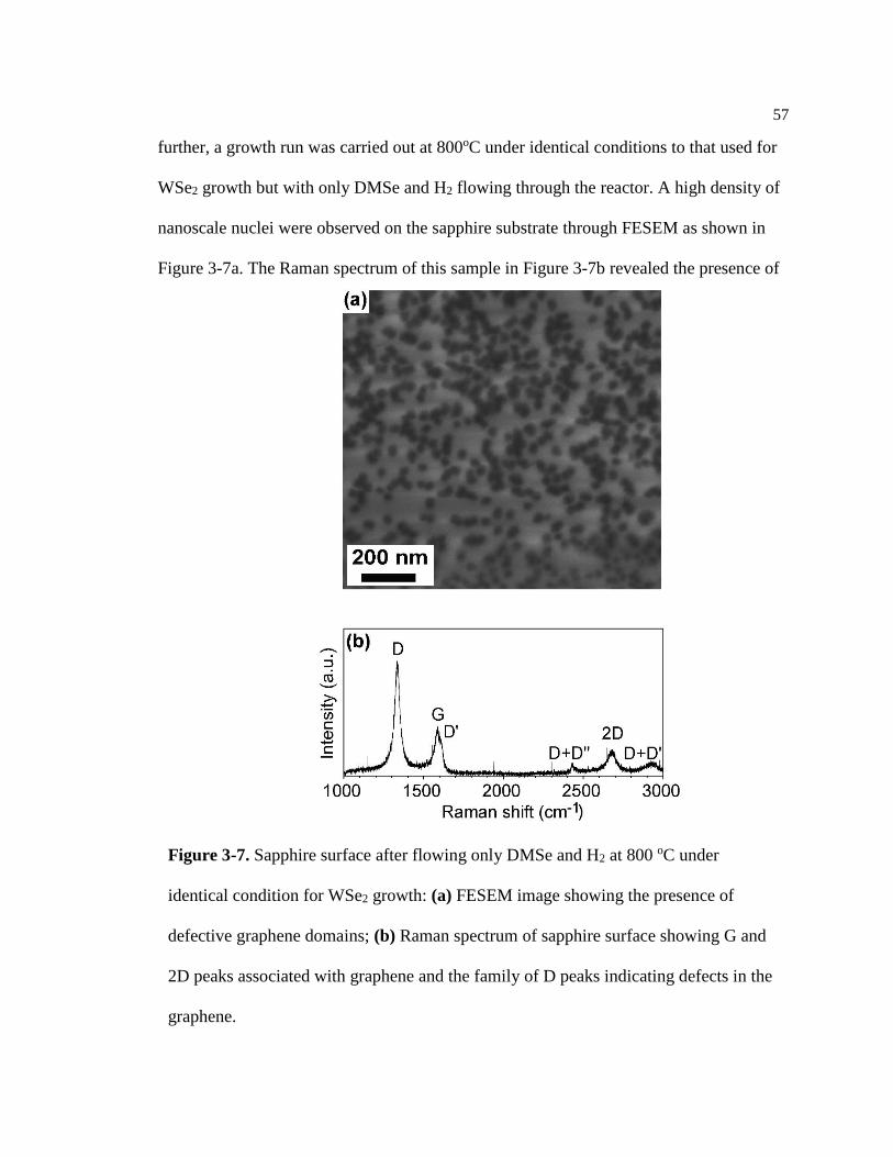
57
further, a growth run was carried out at 800oC under identical conditions to that used for
WSe2 growth but with only DMSe and H2 flowing through the reactor. A high density of
nanoscale nuclei were observed on the sapphire substrate through FESEM as shown in
Figure 3-7a. The Raman spectrum of this sample in Figure 3-7b revealed the presence of
Figure 3-7. Sapphire surface after flowing only DMSe and H2 at 800 oC under
identical condition for WSe2 growth: (a) FESEM image showing the presence of
defective graphene domains; (b) Raman spectrum of sapphire surface showing G and
2D peaks associated with graphene and the family of D peaks indicating defects in the
graphene.

58
peaks associated with defective graphene. The presence of carbon G peak at ~1580 cm-1
and 2D peak at ~2680 cm-1 indicates a graphene-like structure10,12 while the high
intensity of the carbon D peaks indicates that the graphene is highly defective.10,11 The
size of the defective graphene domains is small, less than 50 nm, possibly due to the low
carbon adatom surface diffusion lengths and growth rate at 800oC and the relatively short
30-min growth time. In contrast, the carbon layer in between the WSe2 domains is
continuous with a thickness of 1.5 nm suggesting that the deposition rate of carbon is
higher in the presence of W(CO)6. One interpretation is that the tungsten adatoms on the
surface act as a catalyst to adsorb carbon and promote graphene formation as previously
reported.13
3.4 Chalcogen Precursor: H2Se
3.4.1 Elimination of carbon
Hydride precursors are typically utilized in III-V MOCVD to reduce carbon
incorporation due to their lack of carbon-containing ligands and the atomic hydrogen
produced from hydride decomposition which reacts with methyl groups on the surface to
form methane that can readily desorb from substrate surface.14,15 To investigate the effect
of the chalcogen precursor chemistry, WSe2 films were grown on sapphire using W(CO)6
and H2Se or DMSe using the same Se:W ratio of 3200 and substrate temperature of
800oC. Compared to the growth with DMSe (Figure 3-8a), the Raman spectrum of the
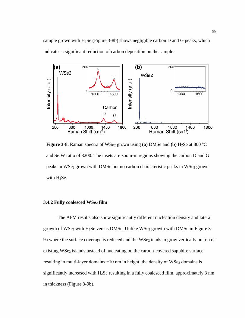
59
sample grown with H2Se (Figure 3-8b) shows negligible carbon D and G peaks, which
indicates a significant reduction of carbon deposition on the sample.
3.4.2 Fully coalesced WSe2 film
The AFM results also show significantly different nucleation density and lateral
growth of WSe2 with H2Se versus DMSe. Unlike WSe2 growth with DMSe in Figure 3-
9a where the surface coverage is reduced and the WSe2 tends to grow vertically on top of
existing WSe2 islands instead of nucleating on the carbon-covered sapphire surface
resulting in multi-layer domains ~10 nm in height, the density of WSe2 domains is
significantly increased with H2Se resulting in a fully coalesced film, approximately 3 nm
in thickness (Figure 3-9b).
Figure 3-8. Raman spectra of WSe2 grown using (a) DMSe and (b) H2Se at 800 oC
and Se:W ratio of 3200. The insets are zoom-in regions showing the carbon D and G
peaks in WSe2 grown with DMSe but no carbon characteristic peaks in WSe2 grown
with H2Se.

60
The defective graphene layer can also be viewed as a competitor to WSe2 on the
substrate surface and thus limits the nucleation as well as the lateral growth of WSe2. As
shown Figure 3-1c and 3-1d, the WSe2 nucleation density decreases but the domain size
does not increase as the Se:W ratio is further increased from 3200 to 4800 and beyond.
Increasing the Se:W results in a higher concentration of methyl radicals in the gas phase,
therefore, more carbon atoms adsorb on the sapphire surface and occupy sites that would
otherwise be available for nucleation and lateral growth of WSe2. As a result, the W and
Se atoms prefer to nucleate and grow on existing WSe2 domains due possibly to site
competition of W, Se and C on the defective graphene surface and/or the reduced surface
energy of the defective graphene compared to WSe2. In either case, the presence of
defective graphene on the sapphire surface increases the vertical-to-lateral growth of the
WSe2 domains. In addition, the WSe2 domains start losing their epitaxy at high Se:W
ratio. It can be interpreted that the defective graphene layer cannot guide the WSe2
domains on top due to its own random orientation, or/and the competition between WSe2
Figure 3-9. AFM images of WSe2 grown using (a) DMSe and (b) H2Se at 800 oC and
Se:W ratio of 3200.

61
and C limits the rotation of initial WSe2 nucleation thus resulting in distorted orientation.
In comparison, the results obtained for WSe2 films grown with H2Se which contain
negligible amounts of carbon support this interpretation. Figure 3-10 shows the TEM
image of the WSe2 film grown with H2Se (done by Fu Zhang, Penn State). The absence
of competing carbon adsorption, diffusion and graphene growth on the sapphire surface
results in a higher nucleation density of WSe2 and nearly complete coalescence of the
films. The inset selected area electron diffraction (SAED) pattern shows a clearly
discernible hexagonal symmetry of the WSe2 film and two main orientations with 30°
Figure 3-10. TEM image of the WSe2 film grown using H2Se at 800 oC and Se:W
ratio of 3200, inset SAED pattern of the yellow circle showing two hexagonal
diffraction patterns with 30° misorientation indicating epitaxial growth of WSe2 on
sapphire.

62
misorientation. This is consistent with previous simulation results for MoS2 grown on
sapphire suggesting the two lowest energy configurations of the epitaxy.16
3.4.3 Toxicity and safety
Hydrogen Selenide (H2Se) is a colorless inorganic acid gas at room temperature. It is also
a flammable and highly toxic gas that requires extra caution when handling.17 It can
attack the eyes and mucus membranes.17 The permissible exposure limit (threshold limit
value) for H2Se is 50 ppb and irritation becomes intolerable at 2 ppm.18 Safe laboratory
use of H2Se requires ventilated enclosures for the gas cylinder, gas handling manifold,
CVD reactor, exhaust pump, etc. Gas lines were welded stainless steel with metal gasket-
seal fittings that were helium leak tested under vacuum. In order to prevent H2Se
exposure to air, all exhaust from the system is run through a chemical scrubber. A NaOH
neutralization system (CVD Equipment Inc. EasyExhaust™) was used to treat the
exhaust gases and a toxic gas detection system (Honeywell Chemcassette®) was in place
for H2Se detection during system operation which can switch off all pneumatic valves to
shut off all gas flow in case of detecting overlimit amount of H2Se or an emergency.
3.5 Conclusions
The results of this study demonstrate the potential problems that may be encountered in
using organic chalcogen precursors in MOCVD growth of very thin TMDs films.
MOCVD provides opportunities for scalability to large wafer sizes, improved thickness

63
and composition uniformity and the ability for in-situ heterostructure growth, however,
carbon deposition as found in our experiments significantly reduces the ability of
MOCVD to produce coalesced WSe2 films with large domain sizes on sapphire
substrates. It is also possible that carbon is incorporated substitutionally within the WSe2
domains or is attached at the domain edge which could further impact the optical and
electrical properties of the films but additional studies are required to determine this.
Also, carbon deposition is expected to be strongly dependent on the particular substrate
used for MOCVD growth and may be less of a problem on amorphous surfaces such as
SiO2/Si which do not typically promote graphene formation. In any event, hydride
chalcogen precursors such as H2Se are good candidates to replace organic chalcogen
precursors used in growth although care must be taken when handling these sources due
to their high toxicity.

64
3.6 References
(1) Kuech, T. F.; Redwing, J. M. Carbon Doping in Metalorganic Vapor Phase
Epitaxy. J. Cryst. Growth 1994, 145 (1–4), 382–389.
(2) Eichfeld, S. M.; Hossain, L.; Lin, Y.; Piasecki, A. F.; Kupp, B.; Birdwell, a G.;
Burke, R. a; Lu, N.; Peng, X.; Li, J.; Azcatl, A.; McDonnell, S.; Wallace, R. M.; Kim, M.
J.; Mayer, T. S.; Redwing, J. M.; Robinson, J. a. Highly Scalable, Atomically Thin WSe2
Grown via Metal–Organic Chemical Vapor Deposition. ACS Nano 2015, 9 (2), 2080–
2087.
(3) Kang, K.; Xie, S.; Huang, L.; Han, Y.; Huang, P. Y.; Mak, K. F.; Kim, C.-J.;
Muller, D.; Park, J. High-Mobility Three-Atom-Thick Semiconducting Films with
Wafer-Scale Homogeneity. Nature 2015, 520 (7549), 656–660.
(4) Wang, S.; Rong, Y.; Fan, Y.; Pacios, M.; Bhaskaran, H.; He, K.; Warner, J. H.
Shape Evolution of Monolayer MoS2 Crystals Grown by Chemical Vapor Deposition.
Chem. Mater. 2014, 26 (22), 6371–6379.
(5) Xie, S.; Xu, M.; Liang, T.; Huang, G.; Wang, S.; Xue, G.; Meng, N.; Xu, Y.;
Chen, H.; Ma, X.; Yang, D. High-Quality Round-Shaped Monolayer MoS2 Domain and
Its Transformation. Nanoscale 2015, 8, 219–225.
(6) Ionescu, R.; George, A.; Ruiz, I.; Favors, Z.; Mutlu, Z.; Liu, C.; Ahmed, K.; Wu,
R.; Jeong, J. S.; Zavala, L.; Mkhoyan, K. A.; Ozkan, M.; Ozkan, C. S. Oxygen Etching of
Thick MoS 2 Films. Chem. Commun. 2014, 50 (76), 11226.
(7) Zhang, K.; Feng, S.; Wang, J.; Azcatl, A.; Lu, N.; Addou, R.; Wang, N.; Zhou,

65
C.; Lerach, J.; Bojan, V.; Kim, M. J.; Chen, L. Q.; Wallace, R. M.; Terrones, M.; Zhu, J.;
Robinson, J. A. Manganese Doping of Monolayer MoS2: The Substrate Is Critical. Nano
Lett. 2015, 15 (10), 6586–6591.
(8) Song, H. J.; Son, M.; Park, C.; Lim, H.; Levendorf, M. P.; Tsen, A. W.; Park, J.;
Choi, H. C. Large Scale Metal-Free Synthesis of Graphene on Sapphire and Transfer-
Free Device Fabrication. Nanoscale 2012, 4 (10), 3050.
(9) Hwang, J.; Kim, M.; Campbell, D.; Alsalman, H. A.; Kwak, J. Y.; Shivaraman,
S.; Woll, A. R.; Singh, A. K.; Hennig, R. G.; Gorantla, S.; Rümmeli, M. H.; Spencer, M.
G. Van Der Waals Epitaxial Growth of Graphene on Sapphire by Chemical Vapor
Deposition without a Metal Catalyst. ACS Nano 2012, 7 (1), 385–395.
(10) Ferrari, A. C.; Basko, D. M. Raman Spectroscopy as a Versatile Tool for
Studying the Properties of Graphene. Nat. Nanotechnol. 2013, 8 (4), 235–246.
(11) Fanton, M. A.; Robinson, J. A.; Puls, C.; Liu, Y.; Hollander, M. J.; Weiland, B.
E.; Labella, M.; Trumbull, K.; Kasarda, R.; Howsare, C.; Stitt, J.; Snyder, D. W.
Characterization of Graphene Films and Transistors Grown on Sapphire by Metal-Free
Chemical Vapor Deposition. ACS Nano 2011, 5 (10), 8062–8069.
(12) Ferrari, A. C.; Meyer, J. C.; Scardaci, V.; Casiraghi, C.; Lazzeri, M.; Mauri, F.;
Piscanec, S.; Jiang, D.; Novoselov, K. S.; Roth, S.; Geim, A. K. The Raman Fingerprint
of Graphene. Phys. Rev. Lett. 2006, 97 (18), 41–47.
(13) Fang, W.; Hsu, A.; Shin, Y. C.; Liao, A.; Huang, S.; Song, Y.; Ling, X.;
Dresselhaus, M. S.; Palacios, T.; Kong, J. Application of Tungsten as a Carbon Sink for

66
Synthesis of Large-Domain Uniform Monolayer Graphene Free of Bilayers/Multilayers.
Nanoscale 2015, 7 (11), 4929–4934.
(14) Fornari, R. Epitaxy for Energy Materials. In Handbook of Crystal Growth: Thin
Films and Epitaxy: Second Edition; 2014; Vol. 3, pp 1–49.
(15) Malik, M. A.; O’Brien, P. Precursors Basic Chemistry of CVD and ALD
Precursors. In Chemical Vapour Deposition: Precursors, Processes and Applications;
Royal Society of Chemistry: Cambridge, 2005; pp 207–271.
(16) Dumcenco, D.; Ovchinnikov, D.; Marinov, K.; Lazić, P.; Gibertini, M.; Marzari,
N.; Sanchez, O. L.; Kung, Y.-C.; Krasnozhon, D.; Chen, M.-W.; Bertolazzi, S.; Gillet, P.;
Fontcuberta i Morral, A.; Radenovic, A.; Kis, A. Large-Area Epitaxial Monolayer MoS2.
ACS Nano 2015, 9 (4), 4611–4620.
(17) HYDROGEN SELENIDE MATERIAL SAFETY DATA SHEET
https://www.mathesongas.com/pdfs/msds/MAT11200.pdf (accessed Mar 17, 2019).
(18) The National Institute for Occupational Safety and Health , Occupational Health
Guideline for Hydrogen Selenide https://www.cdc.gov/niosh/docs/81-123/pdfs/0336.pdf
(accessed Mar 17, 2019).

67
Chapter 4
Diffusion-Controlled Epitaxial Growth of WSe2 on Sapphire
In the previous chapter, we discuss how the unintentional carbon incorporation
from using metalorganic chalcogen precursor can significantly influence the growth of
monolayer or few-layer WSe2 films, and a coalesced film can eventually be achieved
through elimination of carbon contamination via hydride chalcogen precursor. Although
coalesced WSe2 film is achievable, the lack of controllability on both nucleation and
lateral growth makes it extremely hard to approach monolayer growth of WSe2.
Meanwhile, the high nucleation rate of WSe2 nucleation shown in previous chapter
results in two major orientations with 30º rotation and thus the films are far from single
crystal. In this chapter, we demonstrate a multi-step growth process in the same gas
source CVD process for the epitaxial growth of large area, single crystal WSe2 monolayer
and few layer thin films. This multi-step growth process enables independent control of
nucleation, domain ripening, lateral growth and film coalescence and provides
fundamental insights into the 2D growth mechanism. The results in this chapter provide
an important step toward atomic level control of the epitaxial growth of WSe2
monolayers in a scalable process that is suitable for large area device fabrication.
4.1 Introduction
Current development of device technologies based on transition metal
dichalcogenides (TMDs) requires the ability to synthesize large area single crystal

68
monolayer and few layer films. Although powder vapor transport (PVT) has been widely
used to prepare TMD crystal domains and films,1,2 it is difficult to control and modulate
the source supply in this process and uniform deposition over large substrate areas is
challenging. In comparison, gas source chemical vapor deposition (CVD) has both the
metal and chalcogen precursors located outside of the deposition chamber which enables
independent control of precursor partial pressures and ratios. The realization of large
area single crystal TMDC monolayer films, however, requires the ability to precisely
control the density and orientation of nuclei on the substrate surface and the lateral
growth rate of the domains to achieve fully-coalesced 2D monolayer films with minimal
3D growth.
In this chapter, we demonstrate a diffusion-controlled gas source CVD process for
the epitaxial growth of large area, single crystal WSe2 monolayer and few layer films on
c-plane sapphire. A multi-step growth process was developed which employs modulation
of the metal precursor partial pressure to independently control nucleation, domain
ripening, lateral growth and film coalescence via surface diffusion processes. By
separating out the nucleation and lateral growth stages, the effects of process conditions
on surface diffusion and lateral growth can be clearly discerned, providing insights into
the fundamental processes that control WSe2 domain growth.

69
4.2 Experimental Details
4.2.1 Gas source CVD growth conditions
WSe2 films were synthesized in the same cold wall vertical quartz tube reactor
with an inductively heated SiC-coated graphite susceptor. Tungsten hexacarbonyl
(W(CO)6) and hydrogen selenide (H2Se) were used as precursors with ultra-high purity
H2 as the carrier gas. 1 cm×1 cm square C-plane sapphire ((0001) α-Al2O3) were used as
substrates. In a typical growth run, the substrate was heated to the growth temperature
(800 oC) under 700 Torr of H2 at a total flow rate of 450 sccm. A multi-step W(CO)6 flow
process was then used to control nucleation and lateral growth. The precursors (H2Se and
W(CO)6) were simultaneously introduced into the gas stream when the substrate reached
the growth temperature. The H2Se flow rate was held constant at 7 sccm throughout the
entire growth process. The W(CO)6 source powder was contained inside a stainless steel
bubbler which was held at 30 oC and 730 Torr. Initially, H2 carrier gas was passed
through the bubbler at a flow rate of 20 sccm which resulted in a W(CO)6 flow rate of
1.8×10⁻³ sccm out of the bubbler for 0.5-5 min for the nucleation step. The flow rate of
W(CO)6 out of the bubbler was calculated from a mass balance considering the vapor
pressure of the W(CO)6 precursor at 30 oC3,4 and the bubbler pressure at 730 Torr. The
W(CO)6 was then removed from the inlet gas stream and the sample was held in H2Se
and H2 at 800 oC for 0-50 min to allow ripening to occur. Subsequently, for the lateral
growth step, W(CO)6 was re-introduced into the inlet gas stream using a H2 carrier gas
flow rate of 4.5 sccm which resulted in a W(CO)6 flow rate of 4.2×10⁻⁴ sccm. In
additional experiments, the substrate temperature was held constant at 800 oC during the

70
nucleation and ripening steps and was varied from 600 oC to 900 oC during lateral
growth. Studies were also carried out using H2Se flow rates ranging from 4 sccm to 10
sccm during lateral growth to investigate the effect of Se:W ratio.
4.2.2 Film characterization setup
The surface morphology of the samples was analyzed by atomic force microscopy
(AFM) using a Bruker Dimension Icon Atomic Force Microscope system and field
emission scanning electron microscopy (FESEM) using a Zeiss Merlin instrument.
Raman and photoluminescence spectroscopy were carried out using a HORIBA LabRAM
HR Evolution high spectral resolution analytical Raman microscope with a laser
wavelength of 532nm. The composition of the films was investigated by X-ray
photoelectron spectroscopy (XPS) (Phi Versa Probe II) with monochromatic Al Kα x-ray
excitation at 20 kV, equipped with dual beam charge neutralization. Charging offsets
were corrected by calibrating the XPS spectrum based on the C 1s peak position (284.8
eV). Peak fitting was done to confirm the stoichiometry and extent of oxidation of the
films. Reflection high-energy electron diffraction (RHEED) measurement was carried out
using a model RDA-003G electron gun which generates an electron beam of 20 keV and
emission current of 48 μA which was incident on the sample surface at a glancing angle
of ~ 1o. The RHEED pattern was projected on a phosphor screen mounted on a 6-in
flange which was about 20 cm away from the sample and opposite to the electron gun
flange in a vacuum chamber. The RHEED pattern was captured by a digital camera
positioned outside the chamber facing the phosphor screen. The sample was rotated

71
azimuthally with a 1.8o step size increment from 0o to 180o in 100 steps and the
corresponding RHEED pattern was recorded at each azimuthal angle.5 In-plane X-ray
diffraction (XRD) measurements were conducted using a Panlytical MRD diffractometer
with 5 axis cradle employing Cu K radiation and filtering K radiation employing Ni
filter. For transmission electron microscopy (TEM) characterization, the WSe2 film were
transferred from sapphire substrate onto Quantifoil Au TEM grid by a PMMA-assisted
water transfer method. An FEI Titan 3 (60-300) at 80 kV was used to examine and study
the atomic structure of the WSe2 film.
4.3 Single-Step Growth
In chapter 3, we have demonstrated how to achieve a coalesced WSe2 film via
removing carbon contamination and using hydride precursor. It is worth noting that even
the film is fully-coalesced, the small domain sizes and lack of controllability on both film
epitaxy and thickness limit its usage in 2D applications. The coalesced film was grown in
a single-step process where both precursors W(CO)6 and H2Se were maintain at constant
flow rate once the substrate reaches target temperature, and high W(CO)6 flow rate
(~9.0×10⁻⁴ sccm) was adopted to provide enough nucleation for coalesced film (Note:
here “high” is in terms of flow rate used in monolayer TMDs fabrication). The
disadvantage of using high W(CO)6 flow rate is the high growth rate, which results in
both additional nucleation and growth for multilayers and not enough time for domains to
rotate and form single epitaxy. So the question becomes “why don’t we use low W(CO)6
flow rate and long growth time?” Figure 4-1 demonstrate the FESEM image of the

72
sample using very low W(CO)6 flow rate (3.0×10⁻⁴ sccm) and long growth time (90 min).
Indeed, the triangular domains under this condition depict larger domains with ~ 2 μm in
edge length and more epitaxy with fewer 30º rotation. However, the domains fail to fully
coalesce with each other due to limited number of nucleation at low W(CO)6 flow rate,
and the contrast on those domains in FESEM indicate “pyramid” structure formed where
multilayer WSe2 starts to grow on the monolayer. Although WSe2 domains tend to grow
laterally at low W(CO)6 flow rate, the limited surface diffusion length at the growth
temperature is not long enough and the reactant species that fails to diffuse to the edge
either nucleate as second layer or leave the surface. Higher growth temperature should
help but the elevated vapor pressure of Se at higher temperature will result in even higher
flow rate of H2Se. The exceeded Se will condense downstream during the growth and
higher flow rate means a more frequent clean is needed. Further reduction of flow rate of
W(CO)6 should also work and has been demonstrated in previous report,6 however, the
extremely long 24-hour growth time makes the whole process not that feasible.

73
Figure 4-1. FESEM image of WSe2 domains grown at W(CO)6 flow rate of 3.0×10⁻⁴
sccm, H2Se flow rate of 7 sccm, 800 ℃ substrate temperature, and growth time of 90
min.
4.4 Multi-Step Growth
A schematic of the multi-step process employed in this work in shown in Figure
4-2a along with representative AFM images of the sample surface throughout the
process. Tungsten hexacarbonyl (W(CO)6) was initially introduced into the reactor at a
higher flow rate (~1.2×10⁻³ sccm) for 30 sec to drive nucleation on the sapphire surface.
Immediately after this short nucleation step, a high density of W-containing nanoscale
clusters (~5 nm in size) are present on the stepped sapphire surface along with a few
larger particles (Figure 4-2b). The W(CO)6 flow was then removed from the inlet gas

74
stream and the sample was annealed in H2Se for 15 min. During this annealing period,
the density of nanoscale clusters decreased significantly and oriented triangular WSe2
islands with uniform size formed in a process that resembles two-dimensional ripening
(Figure 4-2c). The W(CO)6 was then re-introduced into the inlet gas at a lower flow rate
than the nucleation step (~4.2×10⁻⁴ sccm) to limit further nucleation and promote lateral
growth of the domains (Figure 4-2d).
Figure 4-2. (a) Schematic diagram of the multi-step process showing variation in
W(CO)6 flow rate that was used to control nucleation, ripening and lateral growth. AFM
images of WSe2 grown on sapphire substrate (surface steps aligned horizontally) after (b)
nucleation stage (inset shows the 5 times magnification of the surface, scale bar: 50 nm),
(c) ripening stage, and (d) lateral growth stage.

75
4.5 Nucleation
4.5.1 Initial nucleation clusters
In the initial short nucleation step, a high density of nanoscale clusters revealed on
the substrate surface after cooldown. XPS was carried out to verify the chemical
composition of the W-Se compound formed during the initial nucleation and lateral
growth steps (done by Tanushree Choudhury, Penn State). Figure 4-4 shows high-
resolution scans for Se 3d and W 4f obtained on two samples immediately after the
nucleation step when nanoscale clusters are present on the surface and after the lateral
growth step when the WSe2 monolayer is coalesced. In the case of the coalesced film, the
peak positions for W 4f and Se 3d correspond to WSe2 and the stoichiometry obtained
from the area under the peaks indicates the W to Se ratio to be 1:2. In comparison,
immediately after the nucleation stage, the XPS spectra contains predominant W 4f peaks
and a smaller peak associated with Se 3d indicating that the clusters are W-rich WSex
particles. This is consistent with results from prior cross-section TEM analysis.7 Note that
the W 4f peaks are also shifted to higher binding energy indicating the formation of a
tungsten oxide.3 In this case, the oxide likely forms rapidly when the sample is exposed
to air after removal from the reactor chamber due to the small nanoparticle size and non-
stoichiometric composition.

76
4.5.2 Density of initial WSe2 islands
The nucleation and ripening steps provide a means to control the density, size and
orientation of WSe2 islands which is essential for achieving coalesced monolayer films.
The size and density of WSe2 islands after the nucleation and ripening stages was
controlled by varying the nucleation time. Figure 4-4a shows the surface morphology
under 30 sec, 1 min and 2 min nucleation time respectively and 10 min ripening time.
Figure 4-4b demonstrates the coverage of WSe2 islands on the sapphire surface after 10
Figure 4-3. High-resolution XPS spectra of Se 3d and W 4f for samples (top) after the
lateral growth to form a coalesced WSe2 film and (bottom) immediately after the
nucleation step when nanoscale clusters are present on the surface.
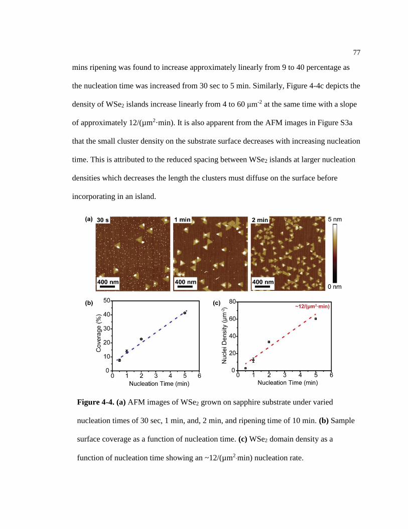
77
mins ripening was found to increase approximately linearly from 9 to 40 percentage as
the nucleation time was increased from 30 sec to 5 min. Similarly, Figure 4-4c depicts the
density of WSe2 islands increase linearly from 4 to 60 μm-2 at the same time with a slope
of approximately 12/(µm2·min). It is also apparent from the AFM images in Figure S3a
that the small cluster density on the substrate surface decreases with increasing nucleation
time. This is attributed to the reduced spacing between WSe2 islands at larger nucleation
densities which decreases the length the clusters must diffuse on the surface before
incorporating in an island.
Figure 4-4. (a) AFM images of WSe2 grown on sapphire substrate under varied
nucleation times of 30 sec, 1 min, and, 2 min, and ripening time of 10 min. (b) Sample
surface coverage as a function of nucleation time. (c) WSe2 domain density as a
function of nucleation time showing an ~12/(µm2·min) nucleation rate.

78
4.6 Ripening
4.6.1 Post-growth characterization
A detailed study of the ripening stage provides insights into surface diffusion
which is the key mechanism responsible for lateral growth of 2D monolayer domains.
Figure 4-5a shows the WSe2 surface morphology grown using a constant nucleation time
of 30 sec and increasing ripening times ranging from 7.5 min to 30 min. As ripening
proceeds, triangular domains start to appear with increasing density and size while the
Figure 4-5. (a) AFM images of WSe2 grown on sapphire substrate under 30 sec
nucleation time and varied ripening time for 7.5, 15, and 30 min. (b) WSe2 domain
size as a function of ripening time and cubic root of ripening time (inset). (c) Cluster
density as a function of ripening time and reciprocal of ripening time (inset). (d)
Substrate surface coverage as a function of ripening time.

79
small clusters between the triangles decrease in number. The size of the triangular
domains (measured by the edge length of the triangle) increases rapidly up to ~200 nm
within the first 15 min of ripening (Figure 4-5b) with a corresponding decrease in cluster
density (Figure 4-5c). During this same time period, the total surface coverage decreases
from 15% to 8.5% (Figure 4-5d) mainly due to differences in the projected areas of
clusters versus triangular WSe2 domains. Beyond 15 min, the domain size, cluster density
and coverage remain relatively constant or decrease only slightly with further annealing
time.
4.6.2 Ripening and surface diffusion
The time dependencies of the domain size and cluster density within the first 15
min are consistent with classical models of 2D ripening8–11 whereby large particles
increase in size as t1/3 (Figure 4-5b inset) and small particles decrease in density as 1/t
(Figure 4-5c inset). The exact mechanism by which ripening occurs is not known
although it is believed to be associated with surface diffusion of W adatoms or migration
of W-rich WSex clusters. A simplified comparison of the vapor pressures of W (<10-6
Torr)12 and Se (~2750 Torr)13 at 800 oC suggests that there should be negligible
desorption of W-containing species from the surface and hence are likely the species
involved in the ripening process. Tungsten-containing adatoms may diffuse from small to
large clusters driven by the concentration gradient resulting from the Gibbs-Thompson
effect (known as Ostwald ripening),10 or the clusters themselves may migrate on the

80
surface and coalesce into larger domains (known as Smoluchowski ripening),11,14 or a
combination of both processes may occur.
4.6.3 Derivation of surface diffusion coefficient
In the case of 2D Smoluchowski ripening, the derivation of surface diffusion
coefficient is based on the following assumptions: the WSe2 cluster size is negligible
compared to the distance between clusters; clusters coalesce into one larger cluster once
they reach each other. The surface diffusion coefficient (D) of the clusters can be
estimated based on Brownian motion and the Einstein equation LD = 2√𝐷𝑡 where LD is
the mean cluster displacement and t is the ripening time.14 The mean cluster displacement
can be approximated as LD ≈ 1/2Lav where Lav is the average distance between clusters.
The schematic plot in Figure 4-6a shows the relationship between LD and Lav. Since all
clusters participate in the coalescence event, any cluster distance smaller than 2LD should
coalesce. Along with the assumption that WSe2 cluster size is negligible, the Lav should
be approximately equal to 2LD, where L𝑎𝑣 = √(1/N). In this way, the cluster density is
then related to the ripening time as 1/N = 16𝐷𝑡. A plot of (1/N) as a function of t
(Figure 4-6b) shows a linear dependence in the first 10 minutes of ripening from which
the cluster surface diffusion coefficient can be estimated as 1.2×10⁻¹⁴ cm2/s. This value
which we associate with the diffusivity of the W-rich WSex particles is comparable to the
diffusivities of ~5 nm Pt particles on alumina (1.5 ×10⁻¹⁴ cm2/s at 600 oC)11 and ~6 nm
Au particles on sapphire (2.0×10⁻¹⁴ cm2/s at 500 oC).15 Note that small clusters are also
present on the top surface of the WSe2 islands after ripening, typically near the edge of a

81
domain (Figure 4-5a). These small clusters have been reported as W-rich WSex
particles,7 which are similar to those present on the sapphire surface that are unable to
migrate over the domain edge due to an Ehrlich-Schwoebel diffusion barrier.16,17
Figure 4-6. (a) Schematic plot showing the method to estimate diffusivity. The average
distance between clusters L𝑎𝑣 = √(1/N), where N is the cluster density. Assume the size
of the cluster is small to be neglected, the estimated mean cluster displacement L𝐷 ≈
1/2L𝑎𝑣. (b) The reciprocal of cluster density as a function of ripening time showing a
linear relationship in the first 10 min with a slope of 2×10⁻³ µm2/min, from which the
diffusivity can be derived as 1.2×10⁻¹⁴ cm2/s.

82
4.7 Lateral Growth
4.7.1 Coalesced monolayer film
To achieve a coalesced monolayer of WSe2, continued nucleation between or on
top of the initial WSe2 islands needs to be suppressed in order to promote lateral growth
of existing domains. Therefore, following the nucleation and ripening steps, the W(CO)6
precursor was reintroduced into the inlet gas stream at a lower flow rate of 4.2×10⁻⁴ sccm
in order to reduce the gas phase supersaturation which is the driving force for crystal
nucleation and growth.18 Figure 4-7a shows scanning electron microscope (SEM) images
of samples grown using 30 sec nucleation time, 15 min ripening time and varied lateral
growth time of 5 min, 20 min, 30 min, and 45 min. Immediately after ripening, the
domains are approximately 120 nm in size and cover 8% of the sapphire surface (t=0 of
Figure 4-7b). As the lateral growth time is increased, the density of triangular domains
remains relatively constant and the domain size and surface coverage increase nearly
linearly with lateral growth time from 5-15 mins (Figure 4-7b). It should be noted that
the lateral growth rate in first 5 min appears to be reduced which is likely due to a short
time lag for the W(CO)6 precursor to reach the substrate after it is re-introduced into the
inlet gas stream. As the surface coverage increases above ~50% (15 mins), however, the
lateral growth rate of the monolayer decreases likely due to precursor adsorption
occurring more frequently on existing WSe2 monolayers rather than on the sapphire
surface. As the WSe2 monolayer domains increase in size, the adatoms must diffuse a
longer distance to reach the domain edges, therefore, it becomes more likely that they
will contribute to bilayer growth instead rather than fill in the initial monolayer. Indeed,

83
the lateral growth rate and coverage of bilayers increases after 15 mins when the
monolayer lateral growth rate decreases (Figure 4-7b). A fully coalesced monolayer with
~36% bilayer coverage across the entire 1 cm×1 cm sapphire substrate can be achieved in
~45 min.
Figure 4-7. (a) SEM images of WSe2 grown on sapphire substrate under 30 sec
nucleation time, 15 min ripening time and varied lateral growth time for 5 min, 20 min,
30 min, and 45 min. (b) WSe2 monolayer domain size and surface coverage as a
function of lateral growth time and bilayer surface coverage as a function of lateral
growth time. A fully coalesced monolayer WSe2 film is achieved in ~45 min lateral
growth. (c) Orientation histogram from 10 min and 20 min samples confirms that WSe2
domain edges are primarily oriented at 0o and 60o with respect to steps on sapphire. (d)
Schematic illustrating 0o and 60o oriented WSe2 domains on sapphire (0001) surface.

84
4.7.2 Preferential orientation
The WSe2 domains clearly exhibit preferred orientations on the (0001) sapphire
surface which begins during the ripening stage (Figure 4-5) and is maintained throughout
the lateral growth stage. A histogram (Figure 4-7c) of domain orientations measured after
5 min, 10 min and 20 min of lateral growth when the domains are still isolated from each
other shows two preferred orientations of 0o and 60o with respect to the step edge
direction which corresponds to the [1120] direction of sapphire, similar to that reported
for epitaxial growth of MoS2 domains on (0001) sapphire substrate by oxide powder
vaporization.19 The preferred orientation results from the commensurability between
WSe2 and sapphire (0001). Although there is large lattice mismatch between WSe2
(a=3.282 Å)20 and sapphire (001) (a=4.760 Å),21 it is reduced to ~3.4% mismatch for 3×3
WSe2 unit cells on a 2×2 (0001) sapphire surface (Figure 3d). Raman and room
temperature photoluminescence (PL) spectroscopy confirm the existence of monolayer
WSe2 due to the absence of a breathing mode at ~310 cm-1 WSe2 (Figure 4-8a)22–25 and a
strong PL peak that varies from 1.60 to 1.64 eV (Figure 4-8b)22 across the sample
surface. Raman mapping (Figure 4-8c) indicates that film is largely monolayer across the
5 m×5 m scan area, however, smaller scale lateral variations are evident from changes
in the Raman peak intensity (Figure 4-8c) and PL peak position (Figure 4-8d). The
lateral non-uniformity may arise from localized Fermi level modulations in the WSe2 due
to surface reconstruction of sapphire at the step edges,26 and/or local variations in strain
in the WSe2 film due to tensile stress that is induced in the film upon cooldown from the
growth temperature due to differences in the coefficients of thermal expansion of WSe2
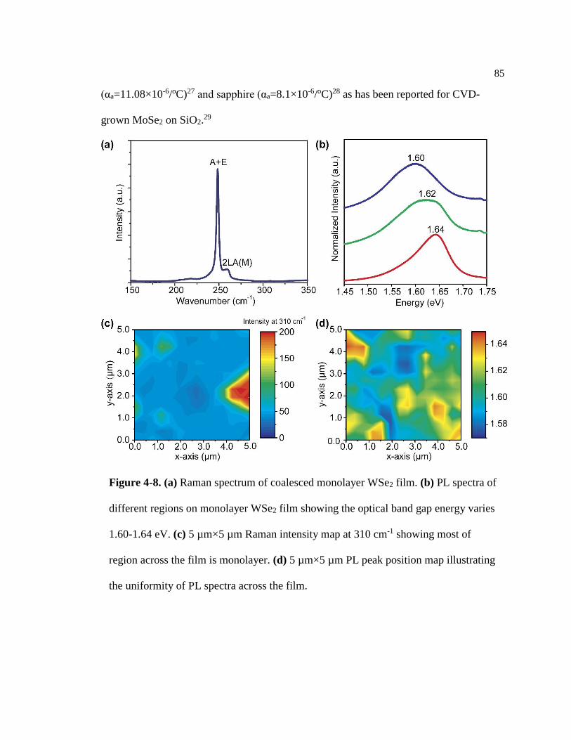
85
(αa=11.08×10⁻⁶/oC)27 and sapphire (αa=8.1×10⁻⁶/oC)28 as has been reported for CVD-
grown MoSe2 on SiO2.29
Figure 4-8. (a) Raman spectrum of coalesced monolayer WSe2 film. (b) PL spectra of
different regions on monolayer WSe2 film showing the optical band gap energy varies
1.60-1.64 eV. (c) 5 µm×5 µm Raman intensity map at 310 cm-1 showing most of
region across the film is monolayer. (d) 5 µm×5 µm PL peak position map illustrating
the uniformity of PL spectra across the film.

86
4.7.3 Substrate temperature effect
The multi-step process also provides a pathway to study the effects of growth
conditions on the domain shape and lateral growth rate independent of their impact on the
nucleation process. For example, Figure 4-9a shows the WSe2 domain morphology after
10 min of lateral growth at 600 oC, 700 oC, 800 oC, and 900 oC with the nucleation and
ripening conditions held constant (30 sec of nucleation and 15 min of ripening at 800 oC)
to maintain a constant initial WSe2 domain density and size. Over the temperature range
from 700 oC to 900 oC, the domain size and density are only weakly dependent on the
growth temperature (Figure 4-9b) suggesting that the growth is limited by mass transport
of precursors to the growth surface as is commonly observed for MOCVD growth of III-
V epilayers.30 This is reasonable considering that both W(CO)6 and H2Se are expected to
decompose in the gas phase at temperatures as low as 375oC,31–33 consequently, WSe2
growth is unlikely to be limited by kinetics at the growth conditions used in this study. At
a lower temperature of 600 oC, however, a bimodal distribution of domain sizes was
observed. The larger domains can be attributed to the initial islands formed during the
nucleation and ripening stages while the smaller domains likely arise from additional
nucleation occurring during the lateral growth step due to reduced surface diffusion at the
lower substrate temperature. In this case, surface adatoms are likely to form new
nucleation sites rather than diffuse to one of the existing WSe2 islands and contribute to
lateral growth.

87
Figure 4-9. (a) SEM images of WSe2 grown on sapphire substrate under 30 sec of
nucleation, 15 min of ripening, and 10 min of lateral growth at varied substrate
temperatures of 600 oC, 700 oC, 800 oC, and 900 oC. H2Se flow rate was held constant at
7 sccm and Se:W ratio was ~26000 during the lateral growth stage. Inset SEM images
show the shape of the WSe2 domains. (b) WSe2 domain size and domain density as a
function of substrate temperature. (c) Schematic diagram showing the variation of WSe2
domain shape under different surface Se:W ratios. (d) SEM image of WSe2 grown under
30 sec of nucleation, 15 min of ripening, and 10 min of lateral growth at substrate
temperature of 900 oC. H2Se flow rate was increased to 10 sccm and Se:W ratio was
~37000 during the lateral growth stage. Inset SEM image shows the shape of WSe2
domain.
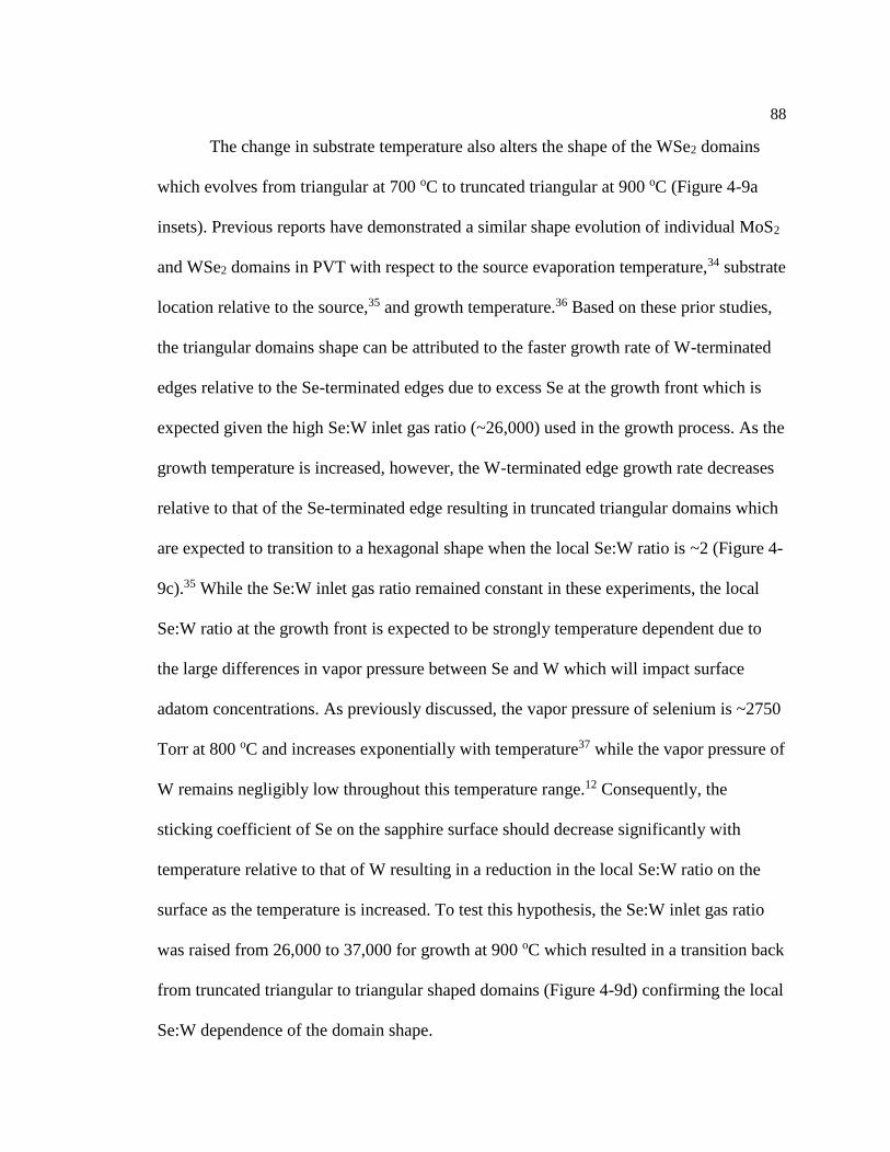
88
The change in substrate temperature also alters the shape of the WSe2 domains
which evolves from triangular at 700 oC to truncated triangular at 900 oC (Figure 4-9a
insets). Previous reports have demonstrated a similar shape evolution of individual MoS2
and WSe2 domains in PVT with respect to the source evaporation temperature,34 substrate
location relative to the source,35 and growth temperature.36 Based on these prior studies,
the triangular domains shape can be attributed to the faster growth rate of W-terminated
edges relative to the Se-terminated edges due to excess Se at the growth front which is
expected given the high Se:W inlet gas ratio (~26,000) used in the growth process. As the
growth temperature is increased, however, the W-terminated edge growth rate decreases
relative to that of the Se-terminated edge resulting in truncated triangular domains which
are expected to transition to a hexagonal shape when the local Se:W ratio is ~2 (Figure 4-
9c).35 While the Se:W inlet gas ratio remained constant in these experiments, the local
Se:W ratio at the growth front is expected to be strongly temperature dependent due to
the large differences in vapor pressure between Se and W which will impact surface
adatom concentrations. As previously discussed, the vapor pressure of selenium is ~2750
Torr at 800 oC and increases exponentially with temperature37 while the vapor pressure of
W remains negligibly low throughout this temperature range.12 Consequently, the
sticking coefficient of Se on the sapphire surface should decrease significantly with
temperature relative to that of W resulting in a reduction in the local Se:W ratio on the
surface as the temperature is increased. To test this hypothesis, the Se:W inlet gas ratio
was raised from 26,000 to 37,000 for growth at 900 oC which resulted in a transition back
from truncated triangular to triangular shaped domains (Figure 4-9d) confirming the local
Se:W dependence of the domain shape.

89
4.8 Structural Characterization
4.8.1 RHEED
4.8.1.1 In-plane lattice constant of WSe2 layer
The RHEED in this chapter was carried out by Yu Xiang at Rensselaer
Polytechnic Institute. For RHEED analysis, the sample was aligned with the sapphire
<1010> parallel to the incident electron beam at the initial position (azimuthal angle φ =
0o). Figures 4-10a and 4-10b show the RHEED patterns from two azimuthal angles about
30o apart, φ = 239.0o and φ = 269.6o, respectively. Figures 4-10c and 4-10d show the
integrated intensity from the yellow dashed box plotted in parallel momentum transfer kǀǀ
direction (parallel to the shadowing edge of the sample) assuming the intensity along
streaks (perpendicular momentum transfer k⊥ direction) is featureless. These peaks are
symmetric with respect to the central streak. From the peaks in Figures 4-10c and 4-10d,
the average adjacent reciprocal spacing between the streaks are measured to be 2.2 ± 0.1
Å-1 and 4.0 ± 0.1 Å-1, respectively. 2H phase WSe2 has a hexagonal lattice with a bulk
lattice constant a = b = 3.2820 Å, c = 12.9600 Å, = = 90o, = 120o. If we choose the
angle between the reciprocal base vectors of WSe2 to be 60o, then |��(ℎ𝑘)| =
4𝜋
√3𝑎√ℎ2 + ℎ𝑘 + 𝑘2. Theoretically, |��(10)| = 2.2106 Å-1, |��(11)| = 3.8289 Å-1. The
measured numbers 2.2 ± 0.1 Å and 4.0 ± 0.1 Å-1 agree very well with the theoretical
calculation for |��(10)| and |��(11)| of WSe2. From the experimentally measured values

90
of |��(ℎ𝑘)|, the lattice constant of WSe2 is determined to be a = 3.2 ± 0.1 Å, which agrees
very well with the bulk value.
4.8.1.2 Reciprocal space structure of WSe2 and its epitaxial relationship with sapphire
The regular orientation of WSe2 domains on the surface of the non-coalesced
samples suggests that the film is epitaxially oriented with respect to the sapphire. This
was confirmed and quantified through RHEED analysis which was carried out on 1 cm×1
cm fully-coalesced monolayer films. Figure 4-11a shows the experimentally measured
Figure 4-10. RHEED patterns of WSe2 collected from 20 keV incident electrons
scattered from two azimuthal angles about 30o apart, (a) φ = 239.0o and (b) φ = 269.6o.
(c) Integrated intensity from the yellow dashed box plotted in parallel momentum
transfer kǀǀ direction in (a). (d) Integrated intensity from the yellow dashed box plotted
in parallel momentum transfer kǀǀ direction in (b).

91
RHEED 2D reciprocal space structure of the WSe2 monolayer plotted as the intensity k∥
(the momentum transfer parallel to the surface) vs. 360o azimuthal directions constructed
from 100 RHEED patterns recorded when the sample was rotated azimuthally with a 1.8°
step size from 0° to 180° in 100 steps as previously demonstrated.38,39 In order to enhance
the signal to noise ratio the intensity at each 𝑘∥ is averaged within the range 2.8 Å-1 <𝑘⊥<
3.1 Å-1. The averaged intensity is then normalized to one. The experimental RHEED 2D
reciprocal space structure shows six-fold symmetry. It also implies if not all or at least the
majority of the WSe2 flakes have the same orientation on α-Al2O3 (0001) substrate.
Figure 4-11b shows the theoretical simulation of 2D reciprocal space structure of WSe2
when the out-of-plane direction is the [0001] direction. The good agreement between
constructed 2D reciprocal space structure of WSe2 and simulated one indicates that the
WSe2 monolayer is nominally single crystal with an epitaxial relation of [1010] WSe2 ‖
[1010] α-Al2O3.
Figure 4-11. (a) Experimentally constructed RHEED 2D reciprocal space structure of
WSe2 plotted as the intensity (k∥) vs. 360o azimuthal directions from 100 RHEED
patterns recorded when the sample was rotated azimuthally with a 1.8° step size from 0°
to 180° in 100 steps. (b) Theoretical simulation of 2D reciprocal space structure of WSe2

92
looking along the out-of-plane [0001] direction which matches the experimental result in
(a), showing [1010] WSe2 ‖ [1010] α-Al2O3.
4.8.2 In-plane XRD
The in-plane XRD in this chapter was carried out by Mikhail Chubarov at Penn
State. The epitaxial relation was also confirmed by in-plane XRD measurements40 which
were carried out across the entire 1cm ×1 cm sample area. The X-ray − scan recorded
using in-plane diffraction geometry at a angle where the 1120 peak of -Al2O3 was
observed, revealed the presence of both WSe2 and substrate 1120 peaks (Figure 4-12a).
Rotation around the surface normal fixing the angle at the 1120 peaks of WSe2 and -
Al2O3 (Figure 4-12b) shows epitaxial growth with an in-plane epitaxial relation of [1120]
WSe2 ‖ [1120] α-Al2O3 which is consistent with RHEED measurement based on the
crystal symmetry of WSe2. The measured full width at half maximum (FWHM) of (1120)
peaks of WSe2 in Figure 4-12b show a narrow value of 0.28º indicating the film is highly
oriented.

93
4.8.3 High Resolution STEM
High resolution scanning transmission electron microscopy (STEM) was done
by Fu Zhang at Penn State and used to further study crystallinity and identify defects and
grain boundaries in WSe2 films removed from the sapphire substrate by a water transfer
process.41 The STEM image (Figure 4-13a) under low magnification and the
corresponding selected area electron diffraction (SAED) pattern (Figure 4-13a inset)
shows that the film consists of a single crystal coalesced monolayer of WSe2 with some
additional bilayer and trilayer growth. High angle annular dark field scanning TEM
(HAADF-STEM) images (Figure 4-13b and 4-13c) display the atomic structure of the
WSe2 film where W and Se atoms can be identified by analyzing the intensity profile due
to the Z-contrast (atomic number) characteristics in the monolayer region of WSe2. A 60°
Figure 4-12. (a) θ-2θ X-ray diffractogram recorded at φ=30° showing reflections
which correspond to (1120) of WSe2 and α-Al2O3. (b) φ-scan recorded at 2θ =37.91°
showing [1120] WSe2 ‖ [1120] α-Al2O3.

94
grain boundary (GB) (inversion domain boundary) is evident in the monolayer region of
WSe2 (marked by red dashed line in Figure 4-13b). Figure 4-13c shows a higher
resolution HAADF-STEM image of the 60° GB that is parallel to the zigzag geometry of
the WSe2 lattice and is stitched together by 4-fold (marked in yellow) and 8-fold (marked
in green) (4|8) rings via point sharing at common Se2 sites. This indicates the formation
of inversion domain boundaries that result from coalescence of 0o and 60o WSe2
domains.42,43
Figure 4-13. (a) Low-magnification TEM image of coalesced WSe2 showing single
layer structure and sequent layers and the corresponding SAED pattern (inset). (b)
Atomic resolution HAADF-STEM image showing the existence of anti-phase grain
boundaries in the film. (c) Higher resolution HAADF-STEM image showing 4|8 rings
attributed to the coalescence of 0o and 60o WSe2 domains.

95
4.9 Conclusions
In summary, this chapter demonstrates a diffusion-controlled gas source CVD
process for the epitaxial growth of large area, fully-coalesced single crystal WSe2
monolayer and few layer films on c-plane sapphire. A multi-step growth process was
developed which employs modulation of the metal precursor partial pressure to
independently control nucleation, domain ripening, lateral growth and film coalescence
via surface diffusion processes. By separating out the nucleation and lateral growth
stages, the effects of process conditions on nucleation density, lateral growth rate and
domain shape can be clearly distinguished, providing experimental insights into the
fundamental mechanisms that control 2D domain growth. The results of this study are an
important step in the development of a reproducible epitaxial growth technology for large
area monolayer TMDC films and 2D heterostructures.

96
4.10 References
(1) Manzeli, S.; Ovchinnikov, D.; Pasquier, D.; Yazyev, O. V.; Kis, A. 2D Transition
Metal Dichalcogenides. Nat. Rev. Mater. 2017, 2 (8), 17033.
(2) Shi, Y.; Li, H.; Li, L.-J. Recent Advances in Controlled Synthesis of Two-
Dimensional Transition Metal Dichalcogenides via Vapour Deposition Techniques.
Chem. Soc. Rev. 2015, 44 (9), 2744–2756.
(3) Lai, K. K.; Lamb, H. H. Tungsten Chemical Vapor Deposition Using Tungsten
Hexacarbonyl: Microstructure of as-Deposited and Annealed Films. Thin Solid Films
2000, 370 (1), 114–121.
(4) Lander, J. J.; Germer, L. H. Plating Molybdenum, Tungsten, and Chromium by
Thermal Decomposition of Their Carbonyls. Trans. Am. Inst. Min. Metall. Eng. 1948,
175, 648–692.
(5) Tang, F.; Parker, T.; Wang, G.-C.; Lu, T.-M. Surface Texture Evolution of
Polycrystalline and Nanostructured Films: RHEED Surface Pole Figure Analysis. J.
Phys. D. Appl. Phys. 2007, 40 (23), R427–R439.
(6) Kang, K.; Xie, S.; Huang, L.; Han, Y.; Huang, P. Y.; Mak, K. F.; Kim, C.-J.;
Muller, D.; Park, J. High-Mobility Three-Atom-Thick Semiconducting Films with
Wafer-Scale Homogeneity. Nature 2015, 520 (7549), 656–660.
(7) Eichfeld, S. M.; Hossain, L.; Lin, Y.; Piasecki, A. F.; Kupp, B.; Birdwell, a G.;
Burke, R. a; Lu, N.; Peng, X.; Li, J.; Azcatl, A.; McDonnell, S.; Wallace, R. M.; Kim, M.
J.; Mayer, T. S.; Redwing, J. M.; Robinson, J. a. Highly Scalable, Atomically Thin WSe2

97
Grown via Metal–Organic Chemical Vapor Deposition. ACS Nano 2015, 9 (2), 2080–
2087.
(8) Baldan, A. Review Progress in Ostwald Ripening Theories and Their
Applications to Nickel-Base Superalloys Part I: Ostwald Ripening Theories. J. Mater.
Sci. 2002, 37 (11), 2171–2202.
(9) Lifshitz, I. M.; Slyozov, V. V. The Kinetics of Precipitation from Supersaturated
Solid Solutions. J. Phys. Chem. Solids 1961, 19 (1–2), 35–50.
(10) Zinke-Allmang, M.; Feldman, L. C.; Grabow, M. H. Clustering on Surfaces. Surf.
Sci. Rep. 1992, 16 (8), 377–463.
(11) Wynblatt, P.; Gjostein, N. A. Supported Metal Crystallites. Prog. Solid State
Chem. 1975, 9 (C), 21–58.
(12) Szwarc, R.; Plante, E. R.; Diamond, J. J. Vapor Pressure and Heat of Sublimation
of Tungsten. J. Res. Natl. Bur. Stand. Sect. A Phys. Chem. 1965, 69A (5), 417.
(13) Brooks, L. S. The Vapor Pressures of Tellurium and Selenium. J. Am. Chem. Soc.
1952, 74 (1), 227–229.
(14) Stoldt, C. R.; Jenks, C. J.; Thiel, P. a.; Cadilhe, a. M.; Evans, J. W.
Smoluchowski Ripening of Ag Islands on Ag(100). J. Chem. Phys. 1999, 111 (11),
5157–5166.
(15) Beszeda, I.; Gontier-Moya, E. G.; Imre, Á. W. Surface Ostwald-Ripening and
Evaporation of Gold Beaded Films on Sapphire. Appl. Phys. A 2005, 81 (4), 673–677.

98
(16) Ehrlich, G.; Hudda, F. G. Atomic View of Surface Self‐Diffusion: Tungsten on
Tungsten. J. Chem. Phys. 1966, 44 (3), 1039–1049.
(17) Schwoebel, R. L.; Shipsey, E. J. Step Motion on Crystal Surfaces. J. Appl. Phys.
1966, 37 (10), 3682–3686.
(18) Cubillas, P.; Anderson, M. W. Synthesis Mechanism: Crystal Growth and
Nucleation. In Zeolites and Catalysis: Synthesis, Reactions and Applications; Wiley-
VCH Verlag GmbH & Co. KGaA: Weinheim, Germany, 2010; Vol. 1, pp 1–55.
(19) Dumcenco, D.; Ovchinnikov, D.; Marinov, K.; Lazić, P.; Gibertini, M.; Marzari,
N.; Sanchez, O. L.; Kung, Y.-C.; Krasnozhon, D.; Chen, M.-W.; Bertolazzi, S.; Gillet, P.;
Fontcuberta i Morral, A.; Radenovic, A.; Kis, A. Large-Area Epitaxial Monolayer MoS2.
ACS Nano 2015, 9 (4), 4611–4620.
(20) Schutte, W. J.; De Boer, J. L.; Jellinek, F. Crystal Structures of Tungsten
Disulfide and Diselenide. J. Solid State Chem. 1987, 70 (2), 207–209.
(21) Tsirelson, V. G.; Yu. Antipin, M.; Gerr, R. G.; Ozerov, R. P.; Struchkov, Y. T.
Ruby Structure Peculiarities Derived from X-Ray Diffraction Data Localization of
Chromium Atoms and Electron Deformation Density. Phys. status solidi 1985, 87 (2),
425–433.
(22) Tonndorf, P.; Schmidt, R.; Böttger, P.; Zhang, X.; Börner, J.; Liebig, A.;
Albrecht, M.; Kloc, C.; Gordan, O.; Zahn, D. R. T.; Michaelis de Vasconcellos, S.;
Bratschitsch, R. Photoluminescence Emission and Raman Response of Monolayer MoS2,
MoSe2, and WSe2. Opt. Express 2013, 21 (4), 4908.

99
(23) Zhao, Y.; Luo, X.; Li, H.; Zhang, J.; Araujo, P. T.; Gan, C. K.; Wu, J.; Zhang, H.;
Quek, S. Y.; Dresselhaus, M. S.; Xiong, Q. Interlayer Breathing and Shear Modes in
Few-Trilayer MoS2 and WSe2. Nano Lett. 2013, 13 (3), 1007–1015.
(24) Del Corro, E.; Terrones, H.; Elias, A.; Fantini, C.; Feng, S.; Nguyen, M. A.;
Mallouk, T. E.; Terrones, M.; Pimenta, M. A. Excited Excitonic States in 1L, 2L, 3L, and
Bulk WSe2 Observed by Resonant Raman Spectroscopy. ACS Nano 2014, 8 (9), 9629–
9635.
(25) Zhao, W.; Ghorannevis, Z.; Amara, K. K.; Pang, J. R.; Toh, M.; Zhang, X.; Kloc,
C.; Tan, P. H.; Eda, G. Lattice Dynamics in Mono- and Few-Layer Sheets of WS2 and
WSe2. Nanoscale 2013, 5 (20), 9677.
(26) Lin, Y.-C.; Jariwala, B.; Bersch, B. M.; Xu, K.; Nie, Y.; Wang, B.; Eichfeld, S.
M.; Zhang, X.; Choudhury, T. H.; Pan, Y.; Addou, R.; Smyth, C. M.; Li, J.; Zhang, K.;
Haque, M. A.; Fölsch, S.; Feenstra, R. M.; Wallace, R. M.; Cho, K.; Fullerton-Shirey, S.
K.; Redwing, J. M.; Robinson, J. A. Realizing Large-Scale, Electronic-Grade Two-
Dimensional Semiconductors. ACS Nano 2018, 12 (2), 965–975.
(27) El-Mahalawy, S. H.; Evans, B. L. The Thermal Expansion of 2 H -MoS 2 , 2 H -
MoSe 2 and 2 H -WSe 2 between 20 and 800°C. J. Appl. Crystallogr. 1976, 9 (5), 403–
406.
(28) Yim, W. M.; Paff, R. J. Thermal Expansion of AlN, Sapphire, and Silicon. J.
Appl. Phys. 1974, 45 (3), 1456–1457.
(29) Krustok, J.; Kaupmees, R.; Jaaniso, R.; Kiisk, V.; Sildos, I.; Li, B.; Gong, Y.

100
Local Strain-Induced Band Gap Fluctuations and Exciton Localization in Aged WS 2
Monolayers. AIP Adv. 2017, 7 (6), 065005.
(30) Biefeld, R. M.; Koleske, D. D.; Cederberg, J. G. The Science and Practice of
Metal-Organic Vapor Phase Epitaxy (MOVPE). In Handbook of Crystal Growth, 2nd Ed.
Thin Films and Epitaxy: Basic Techniques, Vol. IIIA; Kuech, T. F., Ed.; Elsevier, 2015; p
95.
(31) Haigh, J.; Burkhardt, G.; Blake, K. Thermal Decomposition of Tungsten
Hexacarbonyl in Hydrogen, the Production of Thin Tungsten-Rich Layers, and Their
Modification by Plasma Treatment. J. Cryst. Growth 1995, 155 (3–4), 266–271.
(32) PEARSON, R.; HAUGEN, G. Kinetics of the Thermal Decomposition of H2Se.
Int. J. Hydrogen Energy 1981, 6 (5), 509–519.
(33) Lewis, K. E.; Golden, D. M.; Smith, G. P. Organometallic Bond Dissociation
Energies: Laser Pyrolysis of Iron Pentacarbonyl, Chromium Hexacarbonyl, Molybdenum
Hexacarbonyl, and Tungsten Hexacarbonyl. J. Am. Chem. Soc. 1984, 106 (14), 3905–
3912.
(34) Xie, S.; Xu, M.; Liang, T.; Huang, G.; Wang, S.; Xue, G.; Meng, N.; Xu, Y.;
Chen, H.; Ma, X.; Yang, D. A High-Quality Round-Shaped Monolayer MoS2 Domain
and Its Transformation. Nanoscale 2016, 8 (1), 219–225.
(35) Wang, S.; Rong, Y.; Fan, Y.; Pacios, M.; Bhaskaran, H.; He, K.; Warner, J. H.
Shape Evolution of Monolayer MoS2 Crystals Grown by Chemical Vapor Deposition.
Chem. Mater. 2014, 26 (22), 6371–6379.

101
(36) Liu, B.; Fathi, M.; Chen, L.; Abbas, A.; Ma, Y.; Zhou, C. Chemical Vapor
Deposition Growth of Monolayer WSe2 with Tunable Device Characteristics and Growth
Mechanism Study. ACS Nano 2015, 9 (6), 6119–6127.
(37) Brebrick, R. F. Partial Pressure of Se 2 (g) in Selenium Vapor. J. Chem. Phys.
1968, 48 (12), 5741–5743.
(38) Xiang, Y.; Guo, F.-W.; Lu, T.-M.; Wang, G.-C. Reflection High-Energy Electron
Diffraction Measurements of Reciprocal Space Structure of 2D Materials.
Nanotechnology 2016, 27 (48), 485703.
(39) Tang, F.; Parker, T.; Wang, G.-C.; Lu, T.-M. Surface Texture Evolution of
Polycrystalline and Nanostructured Films: RHEED Surface Pole Figure Analysis. J.
Phys. D. Appl. Phys. 2007, 40 (23), R427–R439.
(40) Chubarov, M.; Choudhury, T. H.; Zhang, X.; Redwing, J. M. In-Plane x-Ray
Diffraction for Characterization of Monolayer and Few-Layer Transition Metal
Dichalcogenide Films. Nanotechnology 2018, 29 (5), 055706.
(41) Zhang, F.; Erb, C.; Runkle, L.; Zhang, X.; Alem, N. Etchant-Free Transfer of 2D
Nanostructures. Nanotechnology 2018, 29 (2), 025602.
(42) van der Zande, A. M.; Huang, P. Y.; Chenet, D. A.; Berkelbach, T. C.; You, Y.;
Lee, G.-H.; Heinz, T. F.; Reichman, D. R.; Muller, D. A.; Hone, J. C. Grains and Grain
Boundaries in Highly Crystalline Monolayer Molybdenum Disulphide. Nat. Mater. 2013,
12 (6), 554–561.
(43) Zou, X.; Liu, Y.; Yakobson, B. I. Predicting Dislocations and Grain Boundaries in

102
Two-Dimensional Metal-Disulfides from the First Principles. Nano Lett. 2013, 13 (1),
253–258.

103
Chapter 5
Defect-Controlled Nucleation and Orientation of WSe2 on hBN
This chapter further developed a defect-controlled approach for the nucleation and
epitaxial growth of WSe2 on hBN in a gas source chemical vapor deposition process and
explored the role of single-atom vacancies on the hBN surface in controlling orientation of
WSe2 domains. In previous chapter, inversion domain boundaries become an unsolved
issued in the coalesced monolayer film grown on sapphire substrate. The results in this
chapter reveal an important nucleation mechanism for epitaxial growth of van der Waals
heterostructures and demonstrate hBN as a superior substrate for single crystal transition
metal dichalcogenide films, resulting in a reduced density of inversion domain boundaries
and improved properties. The results motivate further efforts focused on the development
of single crystal hBN substrates and epilayers for synthesis of wafer-scale single crystal
transition metal dichalcogenide films.
5.1 Introduction
The rapid development of device technologies based on 2D transition metal
dichalcogenides (TMDs) and their heterostructures presents increasing demand for
synthesis of wafer-scale high quality single crystal monolayer and few layer films.
Wafer-scale coalesced polycrystalline TMD films on amorphous substrates have been
demonstrated via a hot-wall metalorganic chemical vapor deposition (MOCVD)
process.1–3 To reduce the prevalence of random orientations and high-angle grain

104
boundaries, epitaxial growth of TMD domains or films has been further investigated on
various single crystal substrates such as epitaxial graphene,4–6 hexagonal boron nitride
(hBN),7,8 Au (111),9 and c-plane sapphire.10 The epitaxial growth of TMDs has been
further developed into a wafer-scale process via controlled nucleation and coalescence of
a high density of islands into a continuous film on c-plane sapphire.11 However, inversion
domain boundaries (IDBs) (also referred to as mirror twin grain boundaries) were still
observed in these films resulting from a merging of a mixture of 0º and 180º oriented
domains.5,8,11,12 IDBs have been predicted and experimentally demonstrated to exhibit
metallic character and consequently can serve as conducting channels within the
monolayer that negatively impact both electrical and optical properties.13–16 In addition,
non-uniformities in the optical and transport properties of these TMD films arise from
steps and surface dangling bonds at the interface between the 2D film and 3D
substrate.11,17,18 All of these factors negatively impact the properties of coalesced
monolayer films and also promote undesirable multilayer growth.
In contrast to conventional single crystal substrates (e.g. sapphire), an hBN
substrate offers many potential benefits for the epitaxial growth of large TMD domains.
The basal plane of hBN, in its pristine form, can be considered free of steps and dangling
bonds and is expected to enable reduced nucleation density and high adatom surface
diffusivity. The hexagonal crystal structure of hBN makes it compatible for epitaxial
growth of most 2D TMDs.8,19 In addition, the high dielectric constant and chemically
inert surface of hBN suppresses scattering from charged impurities and substrate
phonons, yielding higher mobilities20–22 and increased exciton densities23,24 in adjacent

105
TMD monolayers. Okada et al. first presented the 0º and 180º oriented domains for WS2
grown on hBN via powder vapor transport (PVT), 32 followed by Yu et al. who
demonstrated the epitaxial growth of MoS2 on hBN via PVT showing these two oriented
domains in approximately equal number similar to that obtained for growth on sapphire.8
However, Fu et al. observed up to 98% preferred orientation for monolayer MoS2
domains grown on hBN by molecular beam epitaxy (MBE).25 Subsequent first-principles
calculations reported by Zhang et al. proposed that the orientation selectivity originates
from single-atom vacancies on the hBN surface that act as nucleation sites and break the
nearly degenerate 0/180º domain orientations.26 Achieving a single preferred orientation
of TMD domains on hBN is highly desired to reduce the density of IDBs in coalesced
epitaxial films, however, little is known about the origin and nature of the single atom
vacancies in hBN responsible for this behavior. In addition, the ability to harness these
defects to control both the nucleation density and orientation of TMD monolayer domains
is highly desired as a pathway to achieve high quality single crystal monolayers over
large areas via coalescence of individual domains.
In this study, we investigate the mechanism of defect-controlled domain
alignment of 2D TMDs on hBN using a combination of experimental studies and first-
principles calculations. The results provide experimental evidence that single-atom
vacancies in hBN trap W atoms and thereby act as nucleation sites that break the
symmetry and selectively stabilize a single preferred WSe2 domain orientation.
Subsequent coalescence of the WSe2 domains leads to monolayer films with reduced

106
IDBs and enhanced photoluminescence and transport properties thereby demonstrating
the significant benefits of hBN as a substrate or template layer for TMD epitaxy.
5.2 Experimental Setup
5.2.1 Substrate preparation
The hBN flakes were mechanically exfoliated (ME) from powder (grade PT 110,
Momentive Performance Materials) and placed on a c-plane sapphire substrate. Both
freestanding ME-hBN transferred onto TEM grid and ME-hBN placed on sapphire
substrate were used as templates to fabricate WSe2/hBN heterostructures by gas source
CVD process.
5.2.2 WSe2 multi-step growth process
The multi-step gas source CVD process developed in chapter 4 was also
employed in this study. Substrate was placed onto a SiC-coated graphite susceptor which
was inductively heated up to 800 ºC under H2 in a cold wall vertical quartz tube reactor.
W(CO)6 was first introduced into the reactor at a high flow rate of 1.2×10⁻³ sccm to drive
nucleation. The W(CO)6 flow was then removed for 10 min which allows surface species
to diffuse and form oriented WSe2 domains. Afterward, the W(CO)6 flow was re-
introduced into the reactor at a lower flow rate of 6.1×10⁻⁴ sccm to promote lateral
growth of the domains. The H2Se flow rate was maintained at 7 sccm during the whole
growth process.
107
5.2.3 Plasma treatment
The hBN flakes on sapphire substrate were exposed to reactive ion etching
treatment. 50 sccm of He gas was introduced into a Tepla M4L Plasma Etch system at a
regulated pressure of 180 mTorr, with a radio frequency (13.56 MHz) power of 50W to
generate He plasma. Different etching times were applied to hBN surfaces while fixing
other plasma generation parameters.
5.2.4 NH3 Annealing
The hBN flakes on sapphire substrate were annealed in a group III-nitride
MOCVD system under NH3/H2 environment for 30 minutes at a temperature of 1100 ºC.
An NH3 flow rate of 1 slm was used and ultra high purity H2 was used as an additional
carrier gas with a total flow rate of 7 slm and reactor pressure of 50 Torr.
5.2.5 Morphology characterization
The surface morphology of the samples was analyzed by atomic force microscopy
(AFM) using a Bruker Dimension Icon Atomic Force Microscope system and field
emission scanning electron microscopy (FESEM) using a Zeiss Merlin instrument.

108
5.2.6 TEM characterization
Scanning transmission electron microscopy (STEM) imaging were carried out on
a FEI Titan3 60-300 microscope operating at 80kV with a monochromated gun and
spherical aberration corrected lenses, providing sub-angstrom resolution. A HAADF
detector was used for the ADF-STEM imaging with a collection angle of 51-300 mrad, a
beam current of 45 pA, and beam convergence angle of 30 mrad (C2 aperture of 70 μm)
for STEM image acquisition. The HREM imaging condition for hBN surface defects was
tuned to a negative Cs to provide white atom contrast at a slight over focus. Imaging of
surface defects on BN carried out at the electron dose of ~5000 e–/Å2·s to minimize
structural damage.27
5.2.7 Photoluminescence measurement
A Renishaw inVia microscope with a Coherent Innova 70C argon-krypton laser
with 488 nm excitation wavelength was used for acquiring the Raman and
photoluminescence (PL) spectra using a backscattering configuration with a 1800
lines/mm grating. PL mapping of both WSe2/hBN and WSe2/sapphire were carried out
using a HORIBA LabRAM HR Evolution high spectral resolution analytical Raman
microscope with a laser wavelength of 532 nm. Temperature-dependent PL spectra were
measured using a Linkam THMS600 optical stage as the sample holder. All the low-
temperature PL spectra were acquired in nitrogen environment.

109
5.2.8 Electrical measurement
The films were transferred onto a 100 nm SiO2 on p++ Si substrate using a PMMA
assisted transfer process (see 2.5 Etch-free Transfer of 2D TMD films).28 The 5 μm
channel regions for the WSe2 on SiO2 and WSe2 on hBN on SiO2 devices were defined
using electron beam lithography (Raith EBPG-5200) and ZEP520A photoresist. The
WSe2 was etched using a SF6/O2 based etch in a Plasma-Therm Versalock etch tool. The
resist was then removed by submersing in 85 °C JT Baker PRS3000 for 30 minutes
followed by an IPA rise. The source drain contacts were patterned using a MMA/PMMA
resist process and the 40 nm Ni/ 30 nm Au metal contacts were deposited via electron
beam evaporation (Kurt J. Lesker Lab-18). Measurements were taken in vacuum (<10-5
Torr) using a Lakeshore CRX-VF probe station and a Keysight B1500A. The hBN
thickness was measured by AFM.
5.2.9 First principles calculations
All first-principles calculations were performed within density functional theory,
using the Perdew-Burke-Ernzerhof parametrization of the generalized gradient
approximation (GGA-PBE) exchange-correlation functional.29,30 Electron-ion interactions
were modeled by projector augmented wave (PAW)31,32 pseudopotentials, as
implemented in the Vienna Ab initio Simulation Package (VASP).33 A semi-empirical
pairwise Van der Waals correction were included using the DFT-D3 method by
Grimme.34 Structural relaxations were performed until forces were smaller than 0.01

110
eV/Å. For the migration barrier of a W adatom on top of WSe2, the nudged elastic band
calculation35 were performed using the climbing image method.36
5.3 Preferential Domain Orientation
WSe2 monolayer films were grown by a multi-step process in a gas source CVD
reactor at 800 ºC using W(CO)6 and H2Se in a H2 carrier gas.23 Single crystal hBN flakes
exfoliated from bulk crystals onto c-plane sapphire ((0001) α-Al2O3) were used as
substrates. In this case, a short 20 min growth time was used to achieve separated WSe2
domains. The WSe2 triangular domains grow epitaxially on the mechanically exfoliated
hBN surface with only two orientations (Figure 5-1a), with the majority of the domains
(~84%) exhibiting a single orientation, and the remainder inversely oriented (Figure 5-
1b). This is different than previous growth outcomes of TMD monolayers on c-plane
sapphire where the epitaxial domains show 0º and 180º oriented domains with nearly
equal proportion.10,11 To directly inspect the structure of laterally stitched regions, a
partially-coalesced WSe2 monolayer on an hBN flake was transferred onto a transmission
electron microscopy (TEM) grid and an area with two types of merging domains –
between the same (region A in Figure 5-1c) and inverse (region B) orientations – was
identified by scanning TEM (STEM) (done by Fu Zhang, Penn State). Figure 5-1d shows
the high angle annular dark field (HAADF-) STEM image (top) and corresponding
inverse fast Fourier transform (FFT) image (after selecting only the WSe2 FFT spots,
bottom) of region A, demonstrating a continuous WSe2 lattice on hBN stitched
seamlessly between the two domains with the same orientation. In contrast, the HAADF-

111
STEM image (top) and corresponding inverse FFT image (bottom) of region B in Figure
1e clearly shows the formation of an IDB between two domains with 0º and 180º
orientation. An atomic resolution HAADF-STEM image along the IDB shows 4|8 ring
motifs (Figure 5-2), consistent with a previous report.12 This demonstrates that the
density of IDBs can be minimized by maximizing the orientational uniformity of WSe2
on hBN, in which case stitching across same-orientation domains would not be troubled
by translationally offset grain boundaries and would not leave an unclosed gap
inaccessible to incoming source molecules.

112
Figure 5-1. (a) AFM image of epitaxial WSe2 domains on hBN. (b) Orientation
histogram of 0o and 180o oriented WSe2 domains on hBN. (c) ADF-STEM image of
region with two types of merging domains. (d) HAADF-STEM image (top) and
corresponding inverse FFT image (bottom) of region A in (c) showing no grain boundary
formed between two domains with same orientation. (e) HAADF-STEM image (top) and
corresponding inverse FFT image (bottom) of region B in (c) showing inversion domain
boundary formed between two domains with 0o and 180o orientation.

113
Figure 5-2. HAADF-STEM image of WSe2 on BN, the anti-phase grain boundary
between the 0º and 60º domains contains 4|8 rings highlighted in the image. It is noted
that a slight sample tilt and high contrast are applied in the imaging condition to blur the
information of underlying BN and the corresponding Moiré patterns between WSe2 and
BN, which help identify the WSe2 lattice.
5.4 Defect-Controlled Nucleation
First-principle calculations previously carried out for MoS2 growth on hBN
suggest the preferred orientation arises from single-atom vacancies on the hBN surface
that lift the 0/180º degeneracy and stabilize one orientation against its inverse.26 In
addition, this mechanism also offers a pathway to control the nucleation density of TMD

114
domains on the surface. To investigate this further, the multi-step growth process from
chapter 4 was adopted for WSe2 growth on hBN which employs modulation of the
W(CO)6 partial pressure to independently control nucleation, domain ripening, and lateral
growth of domains.11 By isolating the nucleation step from the subsequent growth of
domains, insights into the fundamental mechanisms that control WSe2 growth on hBN
can be gleaned. Figure 5-3a shows a series of SEM images of WSe2 grown on hBN and
sapphire surfaces under varied nucleation times of 30 s, 1 min, and 2 min while holding
the times for ripening (10 min) and lateral growth (10 min) constant. For growth on
sapphire, a continuous increase in domain density with increasing nucleation time was
observed (Figure 5-3b). In contrast, the domain of WSe2 on the hBN surface remains
relatively constant density and preferred orientation (Figure 5-4) irrespective of the
nucleation time.
The results can be interpreted using classical nucleation theory,37 whereby the
surface nucleation density N can be expressed as
N = ∫ ns J A exp(−∆G∗
kBT) dt
where ns is the available surface nucleation site density, J is the impingement rate
of precursor molecules, A is the area of the nucleus, ∆G∗ is the energy barrier to reach a
critical nucleation size, T is the growth temperature and t is the nucleation time. In the
case of sapphire, WSe2 can readily nucleate on the surface due to the relatively high
surface energy (from dangling bonds, steps, etc.), which results in a reduced energy
barrier ∆G∗to nucleation. In addition, the available surface nucleation site density ns on
sapphire is large and invariant due to the high concentration of steps and other defects

115
which act as nucleation sites. Since, for the experimental conditions employed, A, ∆G∗, J
and T are constant, the nucleation density N is expected to vary linearly with the growth
time t, which is consistent with the near linear relationship between domain density and
nucleation time experimentally observed on sapphire in Figure 5-3b.
Figure 5-3. (a) SEM images of WSe2 grown on hBN (left) and sapphire (right)
respectively under varied nucleation time of 30 s, 1 min, and 2 min and same 10 min
ripening and growth time. Scale bar: 1 μm. (b) Domain density histogram versus
nucleation time showing the nucleation on hBN is not controlled by the amount of
precursors on the surface.
Figure 5-4. Color-marked SEM images of WSe2 grown on hBN with a preferred
orientation shown in Figure 2a. Scale bar: 1 μm.

116
In comparison, for pristine hBN, the low surface energy associated with the basal
plane vdW surface results in a high nucleation energy barrier ∆G∗ that makes WSe2
nucleation on pristine hBN prohibitively unfavorable, limiting nucleation to hBN defects
(e.g. single atom B or N vacancies), where ∆G∗ is locally reduced. The available surface
nucleation site density ns(t) thus starts equal to the defect density of hBN and becomes
quickly depleted with increasing nucleation time due to the limited number of surface
defects. Consequently, the domain density N saturates and becomes independent of
nucleation time t (Figure 5-4b). Additional evidence of defect-limited nucleation comes
from the non-uniform distribution of WSe2 domains observed on one hBN flake (Figure
5-5), likely due to non-uniformities in the distribution and type of defects formed during
mechanical exfoliation. All of the above observations reflect a defect-controlled
nucleation mechanism for WSe2 growth on hBN.
Figure 5-5. WSe2 grown on pristine hBN surface under 30 s nucleation and 10 min
ripening showing a non-uniform distribution of WSe2 domains.
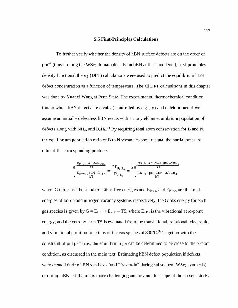
117
5.5 First-Principles Calculations
To further verify whether the density of hBN surface defects are on the order of
μm–2 (thus limiting the WSe2 domain density on hBN at the same level), first-principles
density functional theory (DFT) calculations were used to predict the equilibrium hBN
defect concentration as a function of temperature. The all DFT calcualtions in this chapter
was done by Yuanxi Wang at Penn State. The experimental thermochemical condition
(under which hBN defects are created) controlled by e.g. μN can be determined if we
assume an initially defectless hBN reacts with H2 to yield an equilibrium population of
defects along with NH3, and B2H6.38 By requiring total atom conservation for B and N,
the equilibrium population ratio of B to N vacancies should equal the partial pressure
ratio of the corresponding products
e–EB−vac+μB−EhBN
kT
e–EN−vac+μN−EhBN
kT
=2PB2H6
PNH3
=2e–
GB2H6+2μN−2GBN−3GH2kT
e–GNH3+μB−GBN−3/2GH2
kT
where G terms are the standard Gibbs free energies and EB-vac and EN-vac are the total
energies of boron and nitrogen vacancy systems respectively; the Gibbs energy for each
gas species is given by G = EDFT + EZPE – TS, where EZPE is the vibrational zero-point
energy, and the entropy term TS is evaluated from the translational, rotational, electronic,
and vibrational partition functions of the gas species at 800ºC.39 Together with the
constraint of μB+μN=EhBN, the equilibrium μN can be determined to be close to the N-poor
condition, as discussed in the main text. Estimating hBN defect population if defects
were created during hBN synthesis (and “frozen-in” during subsequent WSe2 synthesis)
or during hBN exfoliation is more challenging and beyond the scope of the present study.

118
As shown in Figure 5-6a, plotting the equilibrium defect density (N0 e –Edef /kT
where N0 is the number of hBN unit cells per area and Edef the defect formation energy)
with respect to temperature, a defect formation energy within the range of 1.5 to 2 eV is
required to reach a defect density on the order of ~1 μm–2 at 800 ºC, as indicated by the
dashed horizontal line. The defect formation energies for N and B vacancies are shown
by the solid lines in Figure 5-6b, as a function of the Fermi energy relative to the valence
band edge of hBN, where the two panels reflect the N-rich (N chemical potential μN set to
the energy of N2) and N-poor limit (B chemical potential μB = EhBN – μN set to the energy
of bulk α-Boron).40 Both simple boron and nitrogen vacancies (VB and VN in solid lines)
and their hydrogenated complexes (dashed lines) are shown. The positive and negative
slopes indicate positively and negatively charged states. Note that the entire range of
Fermi energies is not realistically accessible (e.g. the conduction band edge of hBN is
close to the vacuum level): it is estimated to be 1–2 eV above the valence band edge
since WSe2 exhibits p-type conductivity,41 as marked by the aligned WSe2 bandgap in the
same figure. The equilibrium μN can be determined to be close to the N-poor condition if
we assume hBN defects are created during WSe2 growth, with the lowest defect
formation energy at ~3 eV. Along with additional defects formed during exfoliation, the
above estimates suggest that μm-2 orders of defect densities are achievable by B and N
vacancies in the hBN substrate before growth, leading to the same order of saturated
nucleation densities during WSe2 growth.

119
Figure 5-6. (a) Equilibrium defect concentration for a point defect with formation
energies between 1.5 and 2 eV, as a function of temperature: a defect needs to have a
formation energy in this range to achieve concentrations on the order of μm-2 at 800 ºC.
(b) Defect formation energy for N and B vacancies under N-rich and N-poor conditions,
considering bare vacancies (solid) and hydrogen-passivated ones (dashed). The orange
energy range marks the calculated WSe2 bandgap aligned with that of hBN.
5.6 TEM Investigation
To further probe the role of defects in nucleation and orientation, samples were
prepared using hBN flakes transferred directly onto the TEM grid and then exposed to W
species only in the gas source CVD system using a 30 s pulse of W(CO)6 at 800 ºC. The
defect-assisted nucleation model described previously predicts the presence of an
interstitial transition metal “glue” atom at the single atom vacancies on the hBN surface
which controls the nucleation and orientation of the TMD on the point defect site.26 The
same defect-mediated distinction between 0/180º stacking in WSe2 calculated from DFT
using an 8 × 8 hBN + 6 × 6 WSe2 supercell is 0.90 eV, where the “eclipsed”

120
configuration26 (top and side view in Figure 5-7a) is more stable; the “staggered”
configuration26 that would nucleate a domain with inverse orientation is unfavorable and
suppressed. Compared to Figure 5-7b, which shows the bare ultra-thin hBN flake with
surface defects of one kind (VB or VN), the HAADF-STEM image after W exposure in
Figure 5-7c (done by Fu Zhang, Penn State) shows a single W atom stably trapped on the
hBN surface at a single vacancy site. Furthermore, direct growth of tiny WSe2 domains
on the hBN on a TEM grid was carried out under 30 s nucleation and 5 min ripening. In
the corresponding STEM image shown in Figure 5-7d (done by Fu Zhang, Penn State), a
brighter imaged defect is visible which is consistent with the glue W atom between WSe2
and the underlying hBN. The WSe2 domain also has inevitably formed defects such as
VSe and VSe2. In all of the WSe2 domains examined, the glue W atoms appear within 3-5
nm of the center of the domain. This offset from the exact domain center likely arises
from the fact that during the very early stages of growth, the domain may not grow at the
same rate in all directions due to differences in edge stability and variations in precursor
flux. To further test if the imaged glue W atoms are interstitials trapped at substrate
defects instead of adatoms on top of WSe2, we compare the energy landscape of W atoms
on WSe2 with typical knock-on energies from the imaging electron beam. Using nudged
elastic band calculations at the DFT level, the migration barrier of a surface W adatom is
found to be 0.4 eV (between the ground state at the metal site and the metastable state at
the hollow site, as shown in Figure 5-7e) (done by Yuanxi Wang, Penn State); the
migration barrier of a W adatom between WSe2 and pristine hBN should be similar
(according to similar migration barriers for metal adatoms on monolayer TMDs and
inside bulk TMDs).42 Assuming relativistic binary collisions, the 80 keV electron beam

121
can transfer up to 1.0 eV kinetic energy to a W atom, sufficient for a surface adatom to
hop between lattice sites. In addition, metal atom migration on TMDs has been
previously reported under similar imaging conditions (80 keV).43 Since hopping events
were not seen over the duration of 10 min during STEM scanning, the imaged point-
defects are unlikely to be mobile adatoms or interstitials and are likely trapped
interstitials at vacancy sites in the hBN substrate.

122
Figure 5-7. (a) Top and side view of the relaxed DFT structure of a W interstitial atom
(red) sandwiched between pristine WSe2 and a boron vacancy in hBN. (b) HRTEM
images of monolayer to multilayer pristine hBN at 80 kV with a monochromated electron
source; the intrinsic vacancies in BN is mostly VN on the surface, which is also shown at
the other side of the step edge. (c) HAADF-STEM image of a single W atom trapped at
hBN surface after seeding process (30 s of W(CO)6 flow at 800 ºC), the overlay on the
plot is the corresponding imaging intensity near the single W atom. (d) HAADF-STEM
image of a brighter imaged defect indicating the glue W atom between WSe2 and the
underlying BN (red, top right). The WSe2 domain also has inevitably formed defects such
as VSe and VSe2 (green, bottom right). (e) The migration barrier of a W adatom on a WSe2
surface between the ground state at the (Metal) site and the metastable state at the
(Hollow) site is 0.4 eV from a nudged elastic band calculation.

123
5.7 Controllable Nucleation via Defect Formation and Annealing
5.7.1 He plasma treatment
The fact that WSe2 nucleation is determined by point defects on the hBN surface
motivates a defect-assisted growth mechanism for vdW epitaxy whereby the nucleation
density can be controlled by manipulating surface defect density. In order to test this, He
direct plasma treatment at a RF power of 50 W was employed to intentionally introduce
surface defects on the hBN/sapphire substrates. Figure 5-8 shows the SEM images of
WSe2 grown with 30 s nucleation and 10 min ripening on pristine hBN, hBN treated by 1
s He plasma, and hBN treated by 15 s He plasma, respectively. The short 1 s plasma
treatment has already created a large number of defects on the hBN surface that
significantly increases the WSe2 domain density while still maintaining the epitaxial
growth. Similarly, STEM results also show a consistently increasing density of glue
atoms trapped at the defective surface which act as seeding sites (Figure 5-9 done by Fu
Zhang, Penn State). Note that W atoms are always trapped at one set of BN lattices where
either VB or VN forms, supporting the result of the single preferred orientation growth of
WSe2 domains. The distribution of WSe2 domains on hBN becomes more uniform
(Figure 5-10) at the same time indicating that the defects were created uniformly across
hBN, when compared to the pristine case where additional defects could form during the
mechanical exfoliation. However, the WSe2 domains also start losing the character of
single preferred orientation after the 1 s plasma treatment, possibly because both B and N
single atom vacancies were created simultaneously during the plasma treatment. Longer
plasma treatment can further increase the nucleation density but also heavily damages the
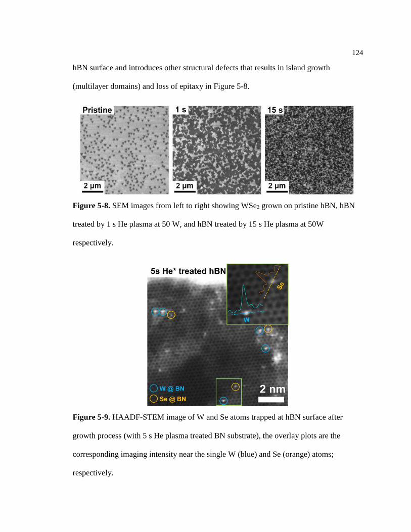
124
hBN surface and introduces other structural defects that results in island growth
(multilayer domains) and loss of epitaxy in Figure 5-8.
Figure 5-8. SEM images from left to right showing WSe2 grown on pristine hBN, hBN
treated by 1 s He plasma at 50 W, and hBN treated by 15 s He plasma at 50W
respectively.
Figure 5-9. HAADF-STEM image of W and Se atoms trapped at hBN surface after
growth process (with 5 s He plasma treated BN substrate), the overlay plots are the
corresponding imaging intensity near the single W (blue) and Se (orange) atoms;
respectively.

125
Figure 5-10. WSe2 grown on 5 s He plasma treated hBN surface under 30 s nucleation
and 10 min ripening showing that the distribution of WSe2 domains on hBN becomes
more uniform.
5.7.2 NH3 annealing
In order to controllably create single atom vacancies of only one element, the
plasma treated hBN surfaces were further annealed in NH3 at 1100 ºC for 30 min to
reduce the concentration of N single atom vacancies. In this case, most of the N
vacancies should be healed and B vacancies should be the majority on the hBN surface.
Figure 5-11 shows SEM images of WSe2 grown with 30 s nucleation and 10 min ripening
on three types of hBN: hBN annealed in NH3, hBN first treated by 1 s He plasma at 50 W
then annealed in NH3, and hBN first treated by 5 s He plasma at 50W then annealed in
NH3. All annealings were performed at 1100 ºC for 30 min. When compared to WSe2

126
grown on pristine hBN, both domain density and percentage of major domain orientation
decrease for WSe2 grown on the NH3 annealed hBN surface (Figure 5-12a and 5-12b).
Native B and N vacancies should exist on pristine hBN while N single atom vacancies
are expected to be the major native defects due to their lower formation energy.44,45 By
healing most of N vacancies during the NH3 annealing, the total single atom vacancy
density decreases, resulting in a decreased density of WSe2 domains. However, not all N
vacancies are expected to be healed and some N vacancies can even reform under the
high temperature (800 ºC) and H2-rich environment during the WSe2 growth process. In
this case, the similar density of N and B vacancies results in the inverse orientations and
thus decreases the percentage of major domain orientation. It is also possible that N
antisite defects (N sitting on B vacancy) could form under NH3 annealing, however we
do not observe a distinctive peak at ~ 623 nm in the room temperature
photoluminescence spectra (Figure 5-13) of the NH3 annealed WSe2/hBN sample which
is associated with antisite defects.46 Consequently, the decrease in nucleation density is
likely not related to a decrease in B vacancies via formation of antisite defects during the
NH3 annealing process.
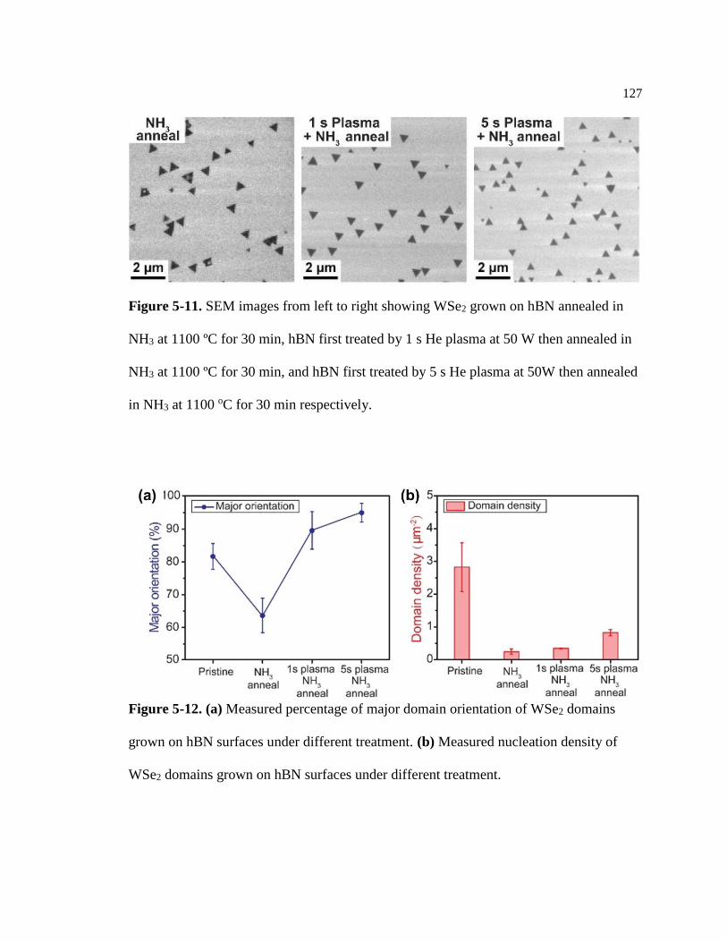
127
Figure 5-11. SEM images from left to right showing WSe2 grown on hBN annealed in
NH3 at 1100 ºC for 30 min, hBN first treated by 1 s He plasma at 50 W then annealed in
NH3 at 1100 ºC for 30 min, and hBN first treated by 5 s He plasma at 50W then annealed
in NH3 at 1100 oC for 30 min respectively.
Figure 5-12. (a) Measured percentage of major domain orientation of WSe2 domains
grown on hBN surfaces under different treatment. (b) Measured nucleation density of
WSe2 domains grown on hBN surfaces under different treatment.

128
Figure 5-13. Room temperature PL spectrum of WSe2/ hBN sample annealed in NH3 at
1100 ºC for 30 min in the region where emission from N antisite defects is expected.
In comparison, on the hBN surface that was first treated by 1 s He plasma then
annealed in NH3, both domain density and the percentage of major domain orientation
WSe2 increase due to the additional B single atom vacancies formed at the hBN surface
from the plasma treatment (Figure 5-12a and 5-12b). By further increasing the plasma
treatment time to 5 s, a 95% major orientation (Figure 5-12a) and ~0.9 μm-2 domain
density (Figure 5-12b) can be achieved. Ideally, 100% single orientation can be
approached by further removing steps, wrinkles and other defects in the hBN and
suppressing N vacancy formation with in-situ NH3 annealing. This defect-assisted
nucleation introduces a useful way to control both the density and orientation of nuclei
when establishing vdW epitaxial growth.

129
5.8 Coalesced Monolayer of WSe2 on hBN
5.8.1 Lateral growth of WSe2 domains
Once the nucleation density of WSe2 on hBN has been controlled, the growth rate
of the WSe2 domains on hBN can be determined for a particular set of growth conditions
by varying the lateral growth time. In this case, the hBN surface was only treated with
NH3 annealing to minimize the density of domains for better observation. The area of
individual WSe2 domains (Figure 5-14a) and the overall surface coverage of WSe2
(Figure 5-14b) increase linearly as the lateral growth time is varied from 10, 15, 30, 60 to
90 min. This indicates that the precursors likely contribute to lateral growth of existing
monolayer domains, rather than nucleating new domains, which is consistent with
observations from atomic force microscopy (AFM) images (Figure 5-14d). It is worth
noting that the measured growth rate for WSe2 monolayers on hBN (~0.35
monolayers/min) is only a quarter of that observed for WSe2 on sapphire (~1.3
monolayers/min),23 even though a higher W(CO)6 flow rate (6.1 × 10⁻⁴ sccm) was used
during the lateral growth step when growing on hBN. This is likely due to the lower
sticking coefficient and higher surface desorption rate of precursors on hBN compared to
sapphire. In comparison, a similar W(CO)6 flow rate (6.8 × 10⁻⁴ sccm) results in a high
nucleation density on sapphire and a multilayer film can be achieved in 30 min.47 This
further validates the defect-controlled mechanism of WSe2 nucleation on hBN. With
appropriate nucleation density of WSe2 achieved by plasma treatment and NH3 annealing
on hBN, continued lateral growth of the initial domains eventually leads to coalescence
into a continuous monolayer film. Figure 5-14c shows a SEM image of a fully coalesced

130
monolayer WSe2 film on an hBN flake. The dark triangular domains in Figure 5c are
additional bilayer domains of WSe2. These bilayer domains possibly arise from additional
nucleation at intrinsic defects in the WSe2 monolayer.
Figure 5-14. (a) WSe2 monolayer domain area on hBN as a function of lateral growth
time. The slope shows a linear growth rate of 7.5 × 10³ nm2/min. (b) WSe2 monolayer
coverage on hBN as a function of lateral growth time. The slope shows a linear growth
rate of 0.58 %/min. (c) SEM image of coalesced monolayer WSe2 film on hBN. (d) AFM
images of WSe2 grown on NH3 annealed hBN surfaces under 30 s nucleation time, 10
min ripening time and varied lateral growth time for 15, 30, and 60 min. The results show
the increasing WSe2 domain size with lateral growth time without any additional
nucleation.

131
5.8.2 Epitaxial relationship between WSe2 and hBN
To further validate and understand the epitaxial relationship between WSe2 and
hBN, a fully coalesced monolayer WSe2 and its underneath substrate hBN flake were
transferred onto a TEM grid together for STEM study (done by Fu Zhang, Penn State).
Figure 5-15a shows an atomic resolution HAADF-STEM image of WSe2 on hBN. The
Moiré patterns of the WSe2/hBN region and the hexagonal crystal structure of the hBN-
only region at the edge indicate an epitaxial growth of monolayer WSe2 on hBN. The
selected area electron diffraction (SAED) pattern of the film shown in Figure 5-15b
identifies the in-plane epitaxial relationship as (1100) WSe2 || (1100) hBN with 0°
misorientation. Based on the Moiré patterns and the lattice constants of WSe2 and hBN,
the mismatch can be reduced to 1.5% for 3 × 3 WSe2 unit cells on 4 × 4 hBN (schematic
in Figure 5-15c).
Figure 5-15. (a) Atomic resolution HAADF-STEM image showing the Moiré pattern of
WSe2 on hBN. (b) SAED pattern showing the epitaxial relationship between WSe2 and
hBN. (c) Schematic illustrating 3 × 3 WSe2 unit cells on 4 × 4 hBN.

132
5.8.3 WSe2/hBN vdW interface
Cross-sectional TEM was also performed on a coalesced WSe2/hBN sample to
further understand the interface between WSe2 and hBN (done by Fu Zhang, Penn State).
A region that contained a tri-layer domain of WSe2 was selected to clearly distinguish the
interlayer spacing. In Figure 5-16a, the regions of hBN, WSe2, and the carbon protection
layer can be distinguished by the crystal structure and interlayer distance. The first layer
of WSe2 shows the highest intensity since it is a fully coalesced monolayer that spans the
entire sample thickness while the second and third layers which are from a portion of an
isolated domain have lower intensity. A clear and sharp interface between WSe2 and hBN
indicates vdW epitaxy occurs with no additional passivating layer. This is different than
growth of WSe2 on sapphire where an extra Se passivating layer and strong WSe2-
substrate bonding at step edges on the sapphire surface were found.18 In addition, a
variation of interlayer distance at the WSe2/hBN interface was also observed. Figure 5-
16b depicts the intensity profile of the red dot line section in Figure 5-16a. Based on the
intensity profile, the interlayer spacing of hBN-hBN and WSe2-WSe2 were measured as
0.33 nm and 0.67 nm, respectively. The spacing between WSe2/hBN, however, was
measured as 0.49 nm, which is nearly identical to the arithmetic mean of the hBN-hBN
and WSe2-WSe2 spacings. This is consistent with the 0.51 nm hBN-WSe2 spacing
calculated from DFT (including the DFT-D3 vdW correction, done by Yuanxi Wang,
Penn State), and with the usual arithmetic mean used for the vdW radii combination rule
in empirical forcefield construction, i.e. Rij = (Ri +Rj)/2 analogous to a hard-sphere
model.48,49

133
Figure 5-16. (a) Cross-sectional HRTEM image of the WSe2 film on hBN showing a
clear WSe2 and hBN interface. (b) Intensity profile of the red dot line in (e) showing the
interlayer spacing of hBN-hBN, hBN-WSe2, and WSe2-WSe2 are 0.33 nm, 0.49 nm, and
0.67 nm respectively.
5.9 Enhanced Optical and Transport Properties
5.9.1 Photoluminescence properties of coalesced WSe2
5.9.1.1 Room temperature PL and mappings
PL spectroscopy is an effective way to optically probe exciton-related emission
and defect states in semiconducting TMDs.50,51 Figure 5-17a shows the PL spectra of
coalesced WSe2/hBN/sapphire and WSe2/sapphire samples grown under identical
conditions using the same power of 488 nm laser excitation. The results show an over 50
× enhancement in PL response for WSe2/hBN compared to WSe2/sapphire. In addition,
the 1.65 eV PL peak position is uniform across the 5 × 5 μm measured area from the

134
WSe2/hBN as shown in Figure 5-17b. In contrast, the PL peak position varied from 1.58
eV to 1.64 eV across the WSe2/sapphire sample. This improvement can be attributed to
the screening effect of the hBN substrate which suppresses the effects of charged
impurities and substrate phonons thereby preserving the intrinsic properties of
WSe2.17,52,53 In comparison, the WSe2 film on sapphire is affected by several factors
including strain and substrate steps, which lead to non-uniformity in PL peak position and
a decrease in PL intensity.
5.9.1.2 Low temperature PL
To further investigate and compare the optical properties of monolayer
WSe2/hBN and WSe2/sapphire, we acquired a series of temperature-dependent PL spectra
from 300 K to 80 K (Figure 6c and 6d, respectively). All the low temperature PL in this
chapter was carried out by Tianyi Zhang in Mauricio Terrones’s lab at Penn State. At
Figure 5-17. (a) PL spectra showing an over 50 × enhancement in intensity for
WSe2/hBN compared to WSe2/sapphire. (b) 5 µm × 5 µm PL maps of coalesced
WSe2/hBN showing a uniform PL peak position at 1.65 eV (top) compared to varied
peak positions ranging from 1.58-1.64 eV for coalesced WSe2/sapphire (bottom).
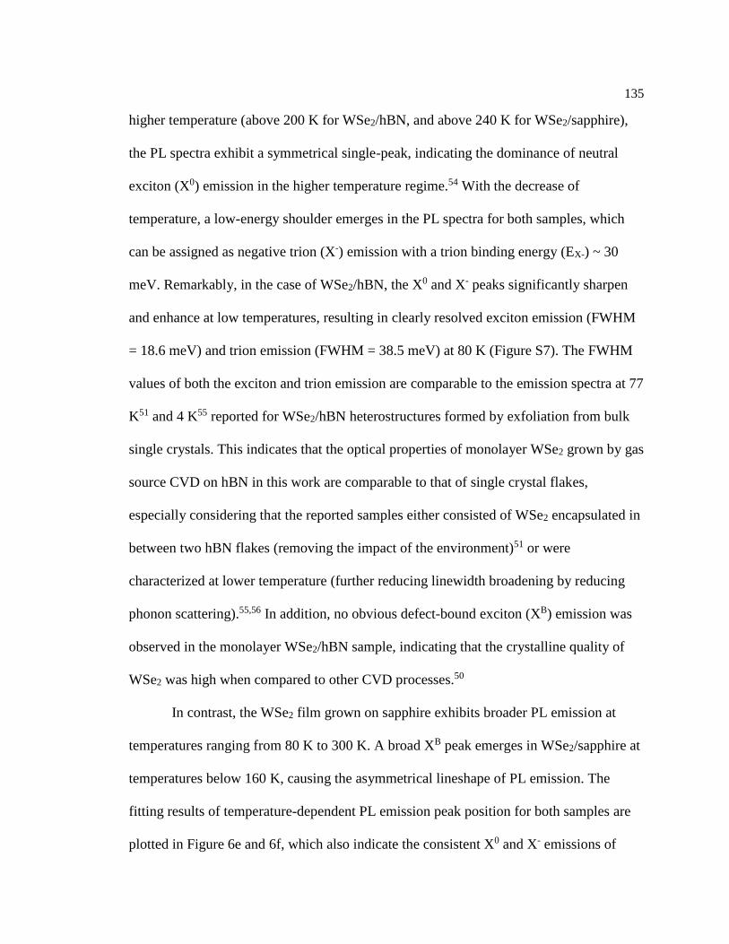
135
higher temperature (above 200 K for WSe2/hBN, and above 240 K for WSe2/sapphire),
the PL spectra exhibit a symmetrical single-peak, indicating the dominance of neutral
exciton (X0) emission in the higher temperature regime.54 With the decrease of
temperature, a low-energy shoulder emerges in the PL spectra for both samples, which
can be assigned as negative trion (X-) emission with a trion binding energy (EX-) ~ 30
meV. Remarkably, in the case of WSe2/hBN, the X0 and X- peaks significantly sharpen
and enhance at low temperatures, resulting in clearly resolved exciton emission (FWHM
= 18.6 meV) and trion emission (FWHM = 38.5 meV) at 80 K (Figure S7). The FWHM
values of both the exciton and trion emission are comparable to the emission spectra at 77
K51 and 4 K55 reported for WSe2/hBN heterostructures formed by exfoliation from bulk
single crystals. This indicates that the optical properties of monolayer WSe2 grown by gas
source CVD on hBN in this work are comparable to that of single crystal flakes,
especially considering that the reported samples either consisted of WSe2 encapsulated in
between two hBN flakes (removing the impact of the environment)51 or were
characterized at lower temperature (further reducing linewidth broadening by reducing
phonon scattering).55,56 In addition, no obvious defect-bound exciton (XB) emission was
observed in the monolayer WSe2/hBN sample, indicating that the crystalline quality of
WSe2 was high when compared to other CVD processes.50
In contrast, the WSe2 film grown on sapphire exhibits broader PL emission at
temperatures ranging from 80 K to 300 K. A broad XB peak emerges in WSe2/sapphire at
temperatures below 160 K, causing the asymmetrical lineshape of PL emission. The
fitting results of temperature-dependent PL emission peak position for both samples are
plotted in Figure 6e and 6f, which also indicate the consistent X0 and X- emissions of

136
WSe2 on hBN at different temperatures, and the emergence of XB emissions from WSe2
on sapphire at low temperature.
The narrower PL linewidths and negligible XB emission for WSe2/hBN compared
to WSe2/sapphire may be attributed to two factors: (1) The direct synthesis on the
atomically-flat hBN surface which leads to a higher crystal quality monolayer WSe2 film
that contains less defects and IDBs, thus decreasing emission from optically-active defect
states; and (2) WSe2 grown on sapphire suffers from the substrate-induced charge
doping,56 which leads to the inhomogeneous broadening of excitonic emissions. By in-
situ synthesizing WSe2 on hBN, the interaction between charged sapphire and WSe2 can
be isolated by the hBN flake, allowing access to the intrinsic optical quality of as-grown
WSe2 films.57,58

137
Figure 5-18. (a)-(b) Temperature-dependent PL spectra of WSe2/hBN and
WSe2/sapphire under 488 nm laser excitation, respectively. The measured temperature
ranges for both samples are from 80 K to 300 K. (c)-(d) Plots of fitted PL emission peak
energy of WSe2/hBN and WSe2/sapphire versus temperature, respectively.
138
Figure 5-19. Deconvoluted PL spectra of WSe2/hBN and WSe2/sapphire at 80 K. The
deconvoluted spectra were acquired by performing multipeak Lorentzian fitting using
three peak components: neutral exciton (X0), trion (X-) and defect-bound exciton (XB).
5.9.2 Transport properties of coalesced WSe2
To characterize the electrical properties of both the WSe2 grown on sapphire and
on hBN, the films were removed from the sapphire substrates and transferred onto 100
nm SiO2 on p++ Si substrates. All the device fabrications in this chapter were carried out
by Daniel Schulman at Penn State. Back gated FETs (BGFETs) with a channel length

139
(LCH) of 1 µm and width (W) of 5 µm were fabricated as shown schematically in Figure
5-20a and 5-20d, respectively. Note that for the growth on hBN, the entire WSe2/hBN
stack was subsequently transferred. In this case, the hBN thickness has been verified as
~10 nm by AFM. Figure 5-20b and 5-20e, show the transfer characteristics i.e. drain
current (IDS) versus back gate voltage (VBG) for different drain voltages (VDS) and Figure
5-20c and 5-20f show the output characteristics i.e. IDS versus VDS for different VBG for
BGFETs based on WSe2 grown on sapphire and hBN, respectively. Clearly, ambipolar
transport i.e. the presence of a prominent electron branch current for VBG > 0 V and hole
branch current for VBG < 0 V are observed for BGFETs based on WSe2 grown on
sapphire as seen in Figure 5-20b. This ambipolar transport is a result of the contact metal
(in this case Ni) Fermi level being pinned near the center of the WSe2 bandgap allowing
injection of electrons and holes into the conduction and the valence band, respectively,
through the corresponding Schottky barriers.59 However, since carriers must tunnel
through relatively large Schottky barrier heights which are almost half the bandgap
energy of WSe2, the corresponding contact resistances for both electron and hole
injections are large, limiting the ON state current as seen in the rectifying type behavior
in Figure 7b. The field effect mobility extracted in the ON state from the peak
transconductance, μFE =∂IDS
∂VGS
LCH
CG W VDS, is severely underestimated in devices with
Schottky barrier contacts.60 For WSe2 grown on sapphire, a contact limited electron µFE
of ~0.3 cm2/Vs was extracted (Figure 5-21a).60 The devices are slightly n-type with an
electron to hole current ratio of ~100:1 indicative of Ni Fermi level pinning closer to the
conduction band. Note that although in the literature there are reports of WSe2 FETs with

140
higher ON state currents and larger electron and hole µFE, these tend to use contact
strategies engineered towards achieving primarily n-type or p-type devices at the expense
of ambipolar characteristics which is achieved with the Ni contacts used in this work.61–63
Figure 5-20. Electrical FET characterization of transferred WSe2 and transferred
WSe2/hBN on SiO2/p++ Si. Schematic showing a back gated WSe2 FETs (a) directly on
100 nm SiO2 and (d) on 10 nm hBN on 100 nm SiO2 on p++ Si with Ni contacts. (b,e)
Drain current (IDS) versus back gate voltage (VBG) at various drain voltages (VDS) with
step of 0.2 V and (c,f) IDS versus VDS at various VBG with step of 2.5 V for WSe2 on SiO2
and on hBN/SiO2, respectively.

141
Figure 5-21. Mobility extraction for WSe2 on SiO2 and hBN/SiO2. (a,b) The field effect
mobility (μFE) versus VBG at VDS = 1.8 V and VDS = -1.8 V for WSe2 on SiO2 and on
hBN/SiO2, respectively. The mobility is derived from the peak transconductance method
where μFE =∂IDS
∂VGS
LCH
CG W VDS. For WSe2 on SiO2, the mobility (μFE ≈ 0.2 cm2/V-s) is
extracted from the reverse sweep direction (negative to positive VBG) since interface trap
discharging obscures the forward sweep characteristics. For WSe2 on hBN/SiO2, the large
contact resistance causes the extracted μFE to decrease when VBG < -43 V. Hence, the
peak mobility of 4.2 cm2/V-s is contact limited, underestimating the true hole mobility of
the material.
For BGFETs based on WSe2 grown on hBN, there is no observable threshold
shift, confirming the growth on hBN has not induced any significant substrate doping
effect. While the electron branch currents are similar to those on SiO2, a dramatic 3
orders of magnitude increase in the hole branch currents is observed. This cannot be

142
attributed to a simple change in the Fermi level pinning since an increase in the hole
branch current would be accompanied by a decrease in the electron branch current. We
hypothesize this hole branch improvement is due to a combination of factors. Part of the
current increase can be attributed to an increase in the hole mobility, due to both a
reduction in the IDBs as well as reduced interface scattering from the hBN versus SiO2
interface. It is well known that hBN encapsulation of 2D materials improves the mobility,
often by orders of magnitude, and reduces the interface states which can cause device
hysteresis and degraded subthreshold slopes.64–66 Second, since the WSe2 is monolayer,
the hBN substrate may influence how the WSe2 hybridizes with the Ni contact in such a
way that hole injection has been facilitated. The charge injection from the contact into the
WSe2 can occur through a combination of many mechanisms and strongly depends on
interface with the metal contact.67 We notice these results are contrary to recent reports
which show devices on hBN have reduced hole branch currents compared to on SiO2.68
The hole µFE extracted from these devices was 4.2 cm2/V-s (Figure 5-21b); however, this
is likely contact limited since the IDS versus VDS characteristics in Figure 5-20f show
rectifying type behavior.60 These results demonstrate that WSe2 growth on hBN is an
effective means to improve the hole transport characteristics and tune FET devices to be
ambipolar or p-type.
5.10 Conclusions
This chapter demonstrates a defect-controlled nucleation and orientation process
for controllable epitaxial growth of single crystal WSe2 monolayers on single crystal hBN

143
flakes. By appropriate plasma treatment and NH3 annealing, the density of single atom
vacancies on the hBN surface, and consequently the nucleation density of single oriented
WSe2, can be controlled. The mechanism of this defect-controlled 2D heterostructure
growth was investigated through first principles calculations and TEM characterization.
A single crystal monolayer film was eventually achieved via coalescence of the initial
domains with extended growth time. PL and electrical measurements show enhanced
optical and transport properties, respectively, for the monolayer WSe2 film grown on
hBN compared to sapphire. Considering that wafer-scale single crystalline hBN has
recently been demonstrated through a CVD method employing a liquid gold substrate,69
this research clearly shows the potential of hBN as a substrate or template layer for
epitaxial growth of high quality single crystal monolayer TMD films.

144
5.11 References
(1) Chiu, M.-H.; Zhang, C.; Shiu, H.-W.; Chuu, C.-P.; Chen, C.-H.; Chang, C.-Y. S.;
Chen, C.-H.; Chou, M.-Y.; Shih, C.-K.; Li, L.-J. Determination of Band Alignment
in the Single-Layer MoS2/WSe2 Heterojunction. Nat. Commun. 2015, 6, 7666.
(2) Kim, T.; Mun, J.; Park, H.; Joung, D.; Diware, M.; Won, C.; Park, J.; Jeong, S.-H.;
Kang, S.-W. Wafer-Scale Production of Highly Uniform Two-Dimensional MoS2
by Metal-Organic Chemical Vapor Deposition. Nanotechnology 2017, 28 (18),
18LT01.
(3) Kalanyan, B.; Kimes, W. A.; Beams, R.; Stranick, S. J.; Garratt, E.; Kalish, I.;
Davydov, A. V.; Kanjolia, R. K.; Maslar, J. E. Rapid Wafer-Scale Growth of
Polycrystalline 2H-MoS2 by Pulsed Metal–Organic Chemical Vapor Deposition.
Chem. Mater. 2017, 29 (15), 6279–6288.
(4) Shi, Y.; Zhou, W.; Lu, A.-Y.; Fang, W.; Lee, Y.-H.; Hsu, A. L.; Kim, S. M.; Kim,
K. K.; Yang, H. Y.; Li, L.-J.; Idrobo, J.-C.; Kong, J. Van Der Waals Epitaxy of
MoS2 Layers Using Graphene As Growth Templates. Nano Lett. 2012, 12 (6),
2784–2791.
(5) Bianco, G. V.; Losurdo, M.; Giangregorio, M. M.; Sacchetti, A.; Prete, P.;
Lovergine, N.; Capezzuto, P.; Bruno, G. Direct Epitaxial CVD Synthesis of
Tungsten Disulfide on Epitaxial and CVD Graphene. RSC Adv. 2015, 5 (119),
98700–98708.
(6) Eichfeld, S. M.; Hossain, L.; Lin, Y.; Piasecki, A. F.; Kupp, B.; Birdwell, a G.;

145
Burke, R. a; Lu, N.; Peng, X.; Li, J.; Azcatl, A.; McDonnell, S.; Wallace, R. M.;
Kim, M. J.; Mayer, T. S.; Redwing, J. M.; Robinson, J. a. Highly Scalable,
Atomically Thin WSe2 Grown via Metal–Organic Chemical Vapor Deposition.
ACS Nano 2015, 9 (2), 2080–2087.
(7) Yan, A.; Velasco, J.; Kahn, S.; Watanabe, K.; Taniguchi, T.; Wang, F.; Crommie,
M. F.; Zettl, A. Direct Growth of Single- and Few-Layer MoS2 on h-BN with
Preferred Relative Rotation Angles. Nano Lett. 2015, 15 (10), 6324–6331.
(8) Yu, H.; Yang, Z.; Du, L.; Zhang, J.; Shi, J.; Chen, W.; Chen, P.; Liao, M.; Zhao,
J.; Meng, J.; Wang, G.; Zhu, J.; Yang, R.; Shi, D.; Gu, L.; Zhang, G. Precisely
Aligned Monolayer MoS2 Epitaxially Grown on h-BN Basal Plane. Small 2017, 13
(7), 1603005.
(9) Zhang, F.; Momeni, K.; AlSaud, M. A.; Azizi, A.; Hainey, M. F.; Redwing, J. M.;
Chen, L.-Q.; Alem, N. Controlled Synthesis of 2D Transition Metal
Dichalcogenides: From Vertical to Planar MoS2. 2D Mater. 2017, 4 (2), 025029.
(10) Dumcenco, D.; Ovchinnikov, D.; Marinov, K.; Lazić, P.; Gibertini, M.; Marzari,
N.; Sanchez, O. L.; Kung, Y.-C.; Krasnozhon, D.; Chen, M.-W.; Bertolazzi, S.;
Gillet, P.; Fontcuberta i Morral, A.; Radenovic, A.; Kis, A. Large-Area Epitaxial
Monolayer MoS2. ACS Nano 2015, 9 (4), 4611–4620.
(11) Zhang, X.; Choudhury, T. H.; Chubarov, M.; Xiang, Y.; Jariwala, B.; Zhang, F.;
Alem, N.; Wang, G.-C.; Robinson, J. A.; Redwing, J. M. Diffusion-Controlled
Epitaxy of Large Area Coalesced WSe2 Monolayers on Sapphire. Nano Lett. 2018,

146
18 (2), 1049–1056.
(12) van der Zande, A. M.; Huang, P. Y.; Chenet, D. A.; Berkelbach, T. C.; You, Y.;
Lee, G.-H.; Heinz, T. F.; Reichman, D. R.; Muller, D. A.; Hone, J. C. Grains and
Grain Boundaries in Highly Crystalline Monolayer Molybdenum Disulphide. Nat.
Mater. 2013, 12 (6), 554–561.
(13) Zou, X.; Liu, Y.; Yakobson, B. I. Predicting Dislocations and Grain Boundaries in
Two-Dimensional Metal-Disulfides from the First Principles. Nano Lett. 2013, 13
(1), 253–258.
(14) Ly, T. H.; Perello, D. J.; Zhao, J.; Deng, Q.; Kim, H.; Han, G. H.; Chae, S. H.;
Jeong, H. Y.; Lee, Y. H. Misorientation-Angle-Dependent Electrical Transport
across Molybdenum Disulfide Grain Boundaries. Nat. Commun. 2016, 7 (1),
10426.
(15) Du, L.; Yu, H.; Xie, L.; Wu, S.; Wang, S.; Lu, X.; Liao, M.; Meng, J.; Zhao, J.;
Zhang, J.; Zhu, J.; Chen, P.; Wang, G.; Yang, R.; Shi, D.; Zhang, G. The Effect of
Twin Grain Boundary Tuned by Temperature on the Electrical Transport
Properties of Monolayer MoS2. Crystals 2016, 6 (9), 115.
(16) Zhou, S.; Wang, S.; Shi, Z.; Sawada, H.; Kirkland, A. I.; Li, J.; Warner, J. H.
Atomically Sharp Interlayer Stacking Shifts at Anti-Phase Grain Boundaries in
Overlapping MoS2 Secondary Layers. Nanoscale 2018, 10 (35), 16692–16702.
(17) Man, M. K. L.; Deckoff-Jones, S.; Winchester, A.; Shi, G.; Gupta, G.; Mohite, A.
D.; Kar, S.; Kioupakis, E.; Talapatra, S.; Dani, K. M. Protecting the Properties of

147
Monolayer MoS2 on Silicon Based Substrates with an Atomically Thin Buffer. Sci.
Rep. 2016, 6 (1), 20890.
(18) Lin, Y.-C.; Jariwala, B.; Bersch, B. M.; Xu, K.; Nie, Y.; Wang, B.; Eichfeld, S.
M.; Zhang, X.; Choudhury, T. H.; Pan, Y.; Addou, R.; Smyth, C. M.; Li, J.; Zhang,
K.; Haque, M. A.; Fölsch, S.; Feenstra, R. M.; Wallace, R. M.; Cho, K.; Fullerton-
Shirey, S. K.; Redwing, J. M.; Robinson, J. A. Realizing Large-Scale, Electronic-
Grade Two-Dimensional Semiconductors. ACS Nano 2018, 12 (2), 965–975.
(19) Okada, M.; Sawazaki, T.; Watanabe, K.; Taniguch, T.; Hibino, H.; Shinohara, H.;
Kitaura, R. Direct Chemical Vapor Deposition Growth of WS2 Atomic Layers on
Hexagonal Boron Nitride. ACS Nano 2014, 8 (8), 8273–8277.
(20) Kretinin, A. V.; Cao, Y.; Tu, J. S.; Yu, G. L.; Jalil, R.; Novoselov, K. S.; Haigh, S.
J.; Gholinia, A.; Mishchenko, A.; Lozada, M.; Georgiou, T.; Woods, C. R.;
Withers, F.; Blake, P.; Eda, G.; Wirsig, A.; Hucho, C.; Watanabe, K.; Taniguchi,
T.; Geim, A. K.; Gorbachev, R. V. Electronic Properties of Graphene Encapsulated
with Different Two-Dimensional Atomic Crystals. Nano Lett. 2014, 14 (6), 3270–
3276.
(21) Mayorov, A. S.; Gorbachev, R. V.; Morozov, S. V.; Britnell, L.; Jalil, R.;
Ponomarenko, L. A.; Blake, P.; Novoselov, K. S.; Watanabe, K.; Taniguchi, T.;
Geim, A. K. Micrometer-Scale Ballistic Transport in Encapsulated Graphene at
Room Temperature. Nano Lett. 2011, 11 (6), 2396–2399.
(22) Ma, N.; Jena, D. Charge Scattering and Mobility in Atomically Thin

148
Semiconductors. Phys. Rev. X 2014, 4 (1), 1–9.
(23) Wierzbowski, J.; Klein, J.; Sigger, F.; Straubinger, C.; Kremser, M.; Taniguchi, T.;
Watanabe, K.; Wurstbauer, U.; Holleitner, A. W.; Kaniber, M.; Müller, K.; Finley,
J. J. Direct Exciton Emission from Atomically Thin Transition Metal
Dichalcogenide Heterostructures near the Lifetime Limit. Sci. Rep. 2017, 7 (1),
12383.
(24) Hoshi, Y.; Kuroda, T.; Okada, M.; Moriya, R.; Masubuchi, S.; Watanabe, K.;
Taniguchi, T.; Kitaura, R.; Machida, T. Suppression of Exciton-Exciton
Annihilation in Tungsten Disulfide Monolayers Encapsulated by Hexagonal Boron
Nitrides. Phys. Rev. B 2017, 95 (24), 241403.
(25) Fu, D.; Zhao, X.; Zhang, Y.; Li, L.; Xu, H.; Jang, A.; Yoon, S. I.; Song, P.; Poh, S.
M.; Ren, T.; Ding, Z.; Fu, W.; Shin, T. J.; Shin, H. S.; Pantelides, S. T.; Zhou, W.;
Loh, K. P. Molecular Beam Epitaxy of Highly Crystalline Monolayer
Molybdenum Disulfide on Hexagonal Boron Nitride. J. Am. Chem. Soc. 2017, 139
(27), 9392–9400.
(26) Zhang, F.; Wang, Y.; Erb, C.; Wang, K.; Moradifar, P.; Crespi, V.; Alem, N. Full
Orientation Control of Epitaxial MoS2 on HBN Assisted by Substrate Defects.
2018.
(27) Meyer, J. C.; Chuvilin, A.; Algara-Siller, G.; Biskupek, J.; Kaiser, U. Selective
Sputtering and Atomic Resolution Imaging of Atomically Thin Boron Nitride
Membranes. Nano Lett. 2009, 9 (7), 2683–2689.

149
(28) Zhang, F.; Erb, C.; Runkle, L.; Zhang, X.; Alem, N. Etchant-Free Transfer of 2D
Nanostructures. Nanotechnology 2018, 29 (2), 025602.
(29) Perdew, J. P.; Burke, K.; Ernzerhof, M. Generalized Gradient Approximation
Made Simple. Phys. Rev. Lett. 1996, 77 (18), 3865–3868.
(30) Perdew, J. P.; Burke, K.; Ernzerhof, M. Erratum: Generalized Gradient
Approximation Made Simple (Physical Review Letters (1996) 77 (3865)). Phys.
Rev. Lett. 1997, 78 (8), 1396.
(31) Joubert, D. From Ultrasoft Pseudopotentials to the Projector Augmented-Wave
Method. Phys. Rev. B - Condens. Matter Mater. Phys. 1999, 59 (3), 1758–1775.
(32) Blöchl, P. E. Projector Augmented-Wave Method. Phys. Rev. B 1994, 50 (24),
17953–17979.
(33) Kresse, G.; Furthmüller, J. Efficient Iterative Schemes for Ab Initio Total-Energy
Calculations Using a Plane-Wave Basis Set. Phys. Rev. B - Condens. Matter
Mater. Phys. 1996, 54 (16), 11169–11186.
(34) Grimme, S.; Antony, J.; Ehrlich, S.; Krieg, H. A Consistent and Accurate Ab Initio
Parametrization of Density Functional Dispersion Correction (DFT-D) for the 94
Elements H-Pu. J. Chem. Phys. 2010, 132 (15), 154104.
(35) JÓNSSON, H.; MILLS, G.; JACOBSEN, K. W. Nudged Elastic Band Method for
Finding Minimum Energy Paths of Transitions. In Classical and Quantum
Dynamics in Condensed Phase Simulations; WORLD SCIENTIFIC, 1998; pp
385–404.

150
(36) Henkelman, G.; Uberuaga, B. P.; Jónsson, H. A Climbing Image Nudged Elastic
Band Method for Finding Saddle Points and Minimum Energy Paths. J. Chem.
Phys. 2000, 113 (22), 9901–9904.
(37) Ohring, M. A Review of Materials Science. In Materials Science of Thin Films;
Elsevier, 2002; pp 1–56.
(38) Ansary, A.; Nasseri, M.; Boland, M. J.; Strachan, D. R. Parallel Boron Nitride
Nanoribbons and Etch Tracks Formed through Catalytic Etching. Nano Res. 2018,
11 (9), 4874–4882.
(39) Cramer, C. J. Essentials of Computational Chemistry: Theories and Models, 2nd
Edition; John Wiley & Sons, 2004.
(40) Weston, L.; Wickramaratne, D.; Mackoit, M.; Alkauskas, A.; Van de Walle, C. G.
Native Point Defects and Impurities in Hexagonal Boron Nitride. Phys. Rev. B
2018, 97 (21), 214104.
(41) Wang, J. I.-J.; Yang, Y.; Chen, Y.-A.; Watanabe, K.; Taniguchi, T.; Churchill, H.
O. H.; Jarillo-Herrero, P. Electronic Transport of Encapsulated Graphene and
WSe2 Devices Fabricated by Pick-up of Prepatterned HBN. Nano Lett. 2015, 15
(3), 1898–1903.
(42) Komsa, H.-P.; Krasheninnikov, A. V. Native Defects in Bulk and Monolayer
MoS2 from First Principles. Phys. Rev. B 2015, 91 (12), 125304.
(43) Lin, Y.-C.; Dumcenco, D. O.; Komsa, H.-P.; Niimi, Y.; Krasheninnikov, A. V.;
Huang, Y.-S.; Suenaga, K. Properties of Individual Dopant Atoms in Single-Layer

151
MoS2 : Atomic Structure, Migration, and Enhanced Reactivity. Adv. Mater. 2014,
26 (18), 2857–2861.
(44) Zobelli, A.; Ewels, C. P.; Gloter, A.; Seifert, G. Vacancy Migration in Hexagonal
Boron Nitride. Phys. Rev. B 2007, 75 (9), 094104.
(45) Wong, D.; Velasco, J.; Ju, L.; Lee, J.; Kahn, S.; Tsai, H.-Z.; Germany, C.;
Taniguchi, T.; Watanabe, K.; Zettl, A.; Wang, F.; Crommie, M. F.
Characterization and Manipulation of Individual Defects in Insulating Hexagonal
Boron Nitride Using Scanning Tunnelling Microscopy. Nat. Nanotechnol. 2015,
10 (11), 949–953.
(46) Tran, T. T.; Bray, K.; Ford, M. J.; Toth, M.; Aharonovich, I. Quantum Emission
from Hexagonal Boron Nitride Monolayers. Nat. Nanotechnol. 2016, 11 (1), 37–
41.
(47) Zhang, X.; Al Balushi, Z. Y.; Zhang, F.; Choudhury, T. H.; Eichfeld, S. M.; Alem,
N.; Jackson, T. N.; Robinson, J. A.; Redwing, J. M. Influence of Carbon in
Metalorganic Chemical Vapor Deposition of Few-Layer WSe2 Thin Films. J.
Electron. Mater. 2016, 45 (12), 6273–6279.
(48) Goodisman, J. Diatomic Interaction Potential Theory; Elsevier, 1973.
(49) Hünenberger, P. H.; van Gunsteren, W. F. Empirical Classical Force Fields for
Molecular Systems; Springer, Berlin, Heidelberg, 1999; pp 177–214.
(50) Carozo, V.; Wang, Y.; Fujisawa, K.; Carvalho, B. R.; McCreary, A.; Feng, S.; Lin,
Z.; Zhou, C.; Perea-López, N.; Elías, A. L.; Kabius, B.; Crespi, V. H.; Terrones,

152
M. Optical Identification of Sulfur Vacancies: Bound Excitons at the Edges of
Monolayer Tungsten Disulfide. Sci. Adv. 2017, 3 (4), e1602813.
(51) Li, X.; Puretzky, A. A.; Sang, X.; KC, S.; Tian, M.; Ceballos, F.; Mahjouri-
Samani, M.; Wang, K.; Unocic, R. R.; Zhao, H.; Duscher, G.; Cooper, V. R.;
Rouleau, C. M.; Geohegan, D. B.; Xiao, K. Suppression of Defects and Deep
Levels Using Isoelectronic Tungsten Substitution in Monolayer MoSe 2. Adv.
Funct. Mater. 2017, 27 (19), 1603850.
(52) Wang, L.; Chen, Z.; Dean, C. R.; Taniguchi, T.; Watanabe, K.; Brus, L. E.; Hone,
J. Negligible Environmental Sensitivity of Graphene in a Hexagonal Boron
Nitride/Graphene/h-BN Sandwich Structure. ACS Nano 2012, 6 (10), 9314–9319.
(53) Jin, C.; Kim, J.; Suh, J.; Shi, Z.; Chen, B.; Fan, X.; Kam, M.; Watanabe, K.;
Taniguchi, T.; Tongay, S.; Zettl, A.; Wu, J.; Wang, F. Interlayer Electron–phonon
Coupling in WSe2/HBN Heterostructures. Nat. Phys. 2017, 13 (2), 127–131.
(54) Huang, J.; Hoang, T. B.; Mikkelsen, M. H. Probing the Origin of Excitonic States
in Monolayer WSe2. Sci. Rep. 2016, 6 (1), 22414.
(55) Lippert, S.; Schneider, L. M.; Renaud, D.; Kang, K. N.; Ajayi, O.; Kuhnert, J.;
Halbich, M.-U.; Abdulmunem, O. M.; Lin, X.; Hassoon, K.; Edalati-Boostan, S.;
Kim, Y. D.; Heimbrodt, W.; Yang, E.-H.; Hone, J. C.; Rahimi-Iman, A. Influence
of the Substrate Material on the Optical Properties of Tungsten Diselenide
Monolayers. 2D Mater. 2017, 4 (2), 025045.
(56) Dey, P.; Paul, J.; Wang, Z.; Stevens, C. E.; Liu, C.; Romero, A. H.; Shan, J.;

153
Hilton, D. J.; Karaiskaj, D. Optical Coherence in Atomic-Monolayer Transition-
Metal Dichalcogenides Limited by Electron-Phonon Interactions. Phys. Rev. Lett.
2016, 116 (12), 127402.
(57) Yu, Y.; Yu, Y.; Xu, C.; Cai, Y. Q.; Su, L.; Zhang, Y.; Zhang, Y. W.; Gundogdu,
K.; Cao, L. Engineering Substrate Interactions for High Luminescence Efficiency
of Transition-Metal Dichalcogenide Monolayers. Adv. Funct. Mater. 2016, 26
(26), 4733–4739.
(58) Cadiz, F.; Courtade, E.; Robert, C.; Wang, G.; Shen, Y.; Cai, H.; Taniguchi, T.;
Watanabe, K.; Carrere, H.; Lagarde, D.; Manca, M.; Amand, T.; Renucci, P.;
Tongay, S.; Marie, X.; Urbaszek, B. Excitonic Linewidth Approaching the
Homogeneous Limit in MoS2-Based van Der Waals Heterostructures. Phys. Rev. X
2017, 7 (2), 1–12.
(59) Das, S.; Appenzeller, J. WSe2 Field Effect Transistors with Enhanced Ambipolar
Characteristics. Appl. Phys. Lett. 2013, 103 (10), 103501.
(60) Nasr, J. R.; Schulman, D. S.; Sebastian, A.; Horn, M. W.; Das, S. Mobility
Deception in Nanoscale Transistors: An Untold Contact Story. Adv. Mater. 2019,
31 (2), 1806020.
(61) Zhou, H.; Wang, C.; Shaw, J. C.; Cheng, R.; Chen, Y.; Huang, X.; Liu, Y.; Weiss,
N. O.; Lin, Z.; Huang, Y.; Duan, X. Large Area Growth and Electrical Properties
of P-Type WSe2 Atomic Layers. Nano Lett. 2015, 15 (1), 709–713.
(62) Fang, H.; Chuang, S.; Chang, T. C.; Takei, K.; Takahashi, T.; Javey, A. High-

154
Performance Single Layered WSe 2 p-FETs with Chemically Doped Contacts.
Nano Lett. 2012, 12 (7), 3788–3792.
(63) Liu, W.; Kang, J.; Sarkar, D.; Khatami, Y.; Jena, D.; Banerjee, K. Role of Metal
Contacts in Designing High-Performance Monolayer n-Type WSe2 Field Effect
Transistors. Nano Lett. 2013, 13 (5), 1983–1990.
(64) Illarionov, Y. Y.; Rzepa, G.; Waltl, M.; Knobloch, T.; Grill, A.; Furchi, M. M.;
Mueller, T.; Grasser, T. The Role of Charge Trapping in MoS2/SiO2and
MoS2/HBN Field-Effect Transistors. 2D Mater. 2016, 3 (3), 035004.
(65) Dean, C. R.; Young, A. F.; Meric, I.; Lee, C.; Wang, L.; Sorgenfrei, S.; Watanabe,
K.; Taniguchi, T.; Kim, P.; Shepard, K. L.; Hone, J. Boron Nitride Substrates for
High-Quality Graphene Electronics. Nat. Nanotechnol. 2010, 5 (10), 722–726.
(66) Wang, J. I.-J.; Yang, Y.; Chen, Y.-A.; Watanabe, K.; Taniguchi, T.; Churchill, H.
O. H.; Jarillo-Herrero, P. Electronic Transport of Encapsulated Graphene and
WSe2 Devices Fabricated by Pick-up of Prepatterned HBN. Nano Lett. 2015, 15
(3), 1898–1903.
(67) Schulman, D. S.; Arnold, A. J.; Das, S. Contact Engineering for 2D Materials and
Devices. Chem. Soc. Rev. 2018, 47 (9), 3037–3058.
(68) Wang, F.; Tu, B.; He, P.; Wang, Z.; Yin, L.; Cheng, R.; Wang, J.; Fang, Q.; He, J.
Uncovering the Conduction Behavior of van Der Waals Ambipolar
Semiconductors. Adv. Mater. 2018, 1805317.
(69) Lee, J. S.; Choi, S. H.; Yun, S. J.; Kim, Y. I.; Boandoh, S.; Park, J.-H.; Shin, B. G.;

155
Ko, H.; Lee, S. H.; Kim, Y.-M.; Lee, Y. H.; Kim, K. K.; Kim, S. M. Wafer-Scale
Single-Crystal Hexagonal Boron Nitride Film via Self-Collimated Grain
Formation. Science 2018, 362 (6416), 817–821.

156
Chapter 6
Low Temperature Growth of Layered Metal Chalcogenides via Metalorganic
Chemical Vapor Deposition
6.1 Motivation
2D materials and especially two-dimensional transition metal dichalcogenides
(2D-TMDs) have attracted wide interest because of their potential performance and
diversity of function as electronic materials. The majority of these efforts have focused
on TMDs such as MoS2 and WSe2, which offer the prospect of ultra-thin channel regions,
high on/off ratios and moderate carrier mobilities. However, growth of transition metal
dichalcogenides (TMDs) typically requires high temperatures (>700oC) for large domain
size and epitaxy. This restricts the applications of these materials, especially considering
the growing interest in 2D materials integration with silicon in back-end-of-line (BEOL)
applications and 3D fabrication and integration in flexible electronics that require
processing temperature < 450oC. Although low-temperature (400 ℃) large area WSe2
film can be obtained via metalorganic chemical vapor deposition (MOCVD) as discussed
in the first part of this chapter, the nanocrystallinity of the films and lack of epitaxy result
in limited performance in transport properties with field effect mobility of ~0.01 cm2/Vs.1
Consequently, TMDs which are “high temperature” materials are not ideal candidates for
2D materials integration using direct deposition approaches.
Instead, there are rising interest in other 2D layered materials, especially in group
IIIA and group IVA metal layered chalcogenides, which also offer intriguing physical
and electronic properties in addition to their typically low melting temperature under

157
900 ℃ (Table 6-1). Recent reports have already shown promising results regarding this
sort of 2D metal chalcogenides. For example, room temperature carrier mobilities ~1000
cm2/Vs for FETs fabricated using exfoliated flakes γ-InSe with hBN-encapsulation.2,3
Fast photoresponsivity within the millisecond level has been demonstrated in both α-
In2Se3 flakes and β-In2Se3 single domains.4,5 In addition, room temperature in-plane and
out-of-plane ferroelectricity has been be explored in α- and β-In2Se3.6–9 Considering the
low melting temperatures of all these materials, depositing crystalline and high quality
films are more feasible at lower temperature which is suitable for BEOL or flexible
electronic applications. In the second part of this chapter, a scalable metalorganic
chemical vapor deposition (MOCVD) growth of epitaxial β-In2Se3 film on both c-plane
sapphire and Si (111) substrate under 400 ℃ with thickness control down to 5 nm is
demonstrated. The relatively high crystalline film grown at low temperature should
enable the development future phase-change memory and photoelectronic application.

158
Table 6-1. Melting temperatures and bulk bandgap energies of selected layered
chalcogenides.
6.2 Low Temperature Growth of WSe2 Films
6.2.1 Growth condition
The WSe2 thin films were grown on thermally oxidized silicon substrates with 50
nm SiO2 using gas source MOCVD system with precursors tungsten hexacarbonyl
(W(CO)6 ) and dimethyl selenium (DMSe). The substrate was heated to 300 ℃ in H2 for
10 mins as a pre-cleaning step. Then the substrate temperature was increased to 400 ℃.
After the temperature was stabilized, 10 sccm of H2 passed through tungsten
hexacarbonyl (W(CO)6) bubbler held at 30 ℃ and 730 Torr which resulted in 6×10⁻⁴
sccm of W(CO)6 out of the bubbler and 12 sccm of H2 passed through dimethyl selenium
(DMSe) bubbler held at room termperature and 760 Torr which resulted in 3.6 sccm of
DMSe out of the bubber. This also leads to a large Se:W ratio of 6300:1. A total flow rate

159
of 450 sccm of H2 was used and the reactor pressure was maintained at 700 Torr during
the growth.
6.2.2 Device Fabrication
The plasma etching and the device fabrication of low-temperature WSe2 was done
by Yiyang Gong at Penn State.10 Plasma etching with O2 was used to pattern WSe2
device areas and to modify film thickness. 100 sccm O2 gas flow was used with the
pressure and dc self-bias maintained at 100 mTorr and -100 V, respectively. No volatile
species are formed and the etching is mainly attributed to the physical bombardment of
oxygen ions, so the etch rate is as low. For the conditions reported here the etch rate for
WSe2 is ~0.25 nm/min.
Arrays of thin film transistors (TFTs) with bottom gate or top gate structures were
fabricated using WSe2 films grown on oxidized silicon wafers. To fabricate bottom gate
TFTs, the WSe2 film was patterned using photolithography and CF4/Ar plasma etching.
For some samples, the patterned WSe2 channels were further thinned using O2 plasma
etching. Next, 50 nm thick Au source and drain contacts were deposited by evaporation
and patterned by photolithography and lift-off. A layer of 50 nm Al2O3 was then
deposited at 200 °C by plasma enhanced atomic layer deposition (PEALD) using
trimethyl aluminum and carbon dioxide as precursors. To reduce the contact resistivity,
the completed devices were annealed in vacuum at 150°C for 10 hours before
measurement. For the top gate TFTs, 100 nm Ti was deposited and patterned by

160
photolithography and lift-off to form gate electrodes on top of the encapsulation layer of
the bottom gate TFTs. For these devices the Al2O3 layer is used as the top gate dielectric.
6.2.3 Film morphology
Under the low temperature regime, MOCVD growth is typically limited by
reaction kinetics and therefore the growth is sensitive to substrate temperature. We have
tested the growth of WSe2 using W(CO)6 and DMSe as precursors starting from 300 ℃.
Below that temperature, no growth happens possibly due to the thermodynamic limit of
precursor decomposition, in this case, most likely to be the DMSe. Figure 6-1a shows an
SEM image of the continuous WSe2 film grown on the oxidized silicon wafer under
400 ℃. At this growth condition, no triangular domains are observed and only numerous
particle-like domains with typical size < 20 nm are covering the whole surface without
any epitaxial signature. This is expected as surface diffusion is significantly limited at
low temperature and only nanocrystalline WSe2 can be formed. Figure 6-1b shows the
Raman spectrum of the WSe2 film measured using the 532 nm wavelength laser source.
The existence of WSe2 in the 2H phase is confirmed by the observation of a single peak
around 250 cm−1, which consists of the degenerate E2g and A1g peaks standing for the in-
plane and out-of-plane modes.11–14 Atomic force microscopy was used to characterize the
thickness and surface roughness of the WSe2 films. Figure 6-1c shows an AFM image
taken at a scratched boundary (by plastic tweezer) of a ~3 nm WSe2 film. The thickness
of the film is estimated as the height of the step using the cross-section profile. Note that
even though the film presents as nanocrystalline, the film RMS roughness is relatively

161
low as ~1.0 nm. In addition, a steady linear relationship between film thickness and
growth time is achieved under this condition as shown in Figure 6-1d. In the first stage,
from 0 to 10 mins, the growth shows a delay in the first 10 min possibly due to the initial
nucleation of WSe2 on the oxidized silicon wafer. From 10 to 30 mins, the growth rate is
linearly around 0.3 nm/min.
Figure 6-1. (a) SEM image of continuous WSe2 thin film on SiO2/Si substrate. (b)
Raman spectrum of ~3 nm WSe2 thin film. (c) AFM image of 3 nm thick WSe2 thin film.
(d) WSe2 film thickness as function of growth time.

162
6.2.4 Device characterization
To investigate the electrical properties of the low-temperature MOCVD WSe2
films, arrays of TFTs were fabricated using 6 nm and 3 nm thick as-grown WSe2 films.
Figure 6-2 shows schematic and optical images of double gate WSe2 TFTs (these devices
have both top and bottom gates). The WSe2 TFT channel width varies from 10 µm to 200
µm and the channel length varies from 2 µm to 50 µm. Figure 6-3a shows the ID-VDS
characteristics of a TFT with 6 nm thick WSe2 and 20/10 µm channel width/length. In the
measurement, the drain-to-source voltage is swept from 0 V to -30 V, and the top gate
voltage varied from 10 V to – 30 V in steps of -10 V. P-channel behavior and well-
defined drain current saturation can be observed. The on-off current ratio is ~100. The
high off state current (~1.1×10⁻⁸ A when VDS=-10 V) indicates that the conductivity of
the 6 nm WSe2 film is high and that thinner films should be used for lower off state
current and higher on-off ratio. Figure 6-3b shows the ID-VDS characteristics of a TFT
with 3 nm thick WSe2 film and 200/5 µm channel width/length. In this measurement, the
drain-to-source voltage is swept from 0 V to 15 V, and the bottom gate voltage is varied
from -10 V to 30 V in steps of 10 V. The device has high resistance and only weak n-
channel behavior, with maximum drain current lower than 10-9 A.

163
Figure 6-2. (a) Cross-section and (b) optical microscopic image of a double gate WSe2
TFT. (c) Array of WSe2 TFTs.
Figure 6-3. ID-VDS characteristics of WSe2 TFTs using as-grown film. (a) Top gate TFT
with 6 nm thick channel and (b) bottom gate TFT with 3 nm thick channel.
To further understand the thickness dependent electrical properties of the
MOCVD WSe2 thin films, TFTs were fabricated with a 6 nm thick WSe2 film thinned to
3 nm using oxygen plasma etching. Figure 6-4a shows the ID-VDS characteristics of TFTs
with channel length/width = 2/200 µm and 50/200 µm, respectively. The on-off ratio of
the device is improved to greater than 104 while the off state current is limited to below

164
10-11 A. Figure 6-4b shows the ID-VDS characteristics for VDS = -3V and -20V. The linear
region differential field effect mobility is extracted using
Dg
d
linearVCW
L
V
I 11
d
d=
,
where L and W are the length and the width of the channel, C is the unit area capacitance
of the gate dielectric, and VD is the drain-to-source voltage. When VG = -35 V and VDS = -
20 V, the extracted field effect mobility is ~0.01 cm2/Vs. The turn-on voltages for VDS = -
3 V and VDS = -20 V are ~5 V and ~0 V, respectively. The devices have significant
hysteresis, possibly due to a high trap density in the WSe2 film or at the WSe2/dielectric
interface. Though further investigation is needed to understand the significant difference
in device performance between as-grown 3 nm thick WSe2 and plasma thinned 3 nm
thick WSe2, our results demonstrate that plasma etching provides an additional degree of
freedom to modulate the electrical properties of CVD WSe2 thin films.
Figure 6-4. (a) ID-VDS and (b) ID-VG characteristics of WSe2 TFTs using 3 nm thick RIE
thinned film.

165
To estimate the impact of contacts on the device, the resistance of TFTs was
extracted from linear region (VDS = 0.4 V) ID-VDS characteristics. Figure 6-5a shows the
total resistance, RTOT = RCH + 2 RC, for TFTs with different channel lengths and for two
gate voltages, where RCH and RC represent the channel resistance and contact resistance,
respectively. The resistance of contact and channel for VG= -10 V and -20 V are shown in
Figure 6-5b. The contact resistance is gate voltage dependent as expected for Schottky
barrier contacts. While both channel resistance and contact resistance decrease as gate
voltage increases from -10 V to -20 V, the contact resistance dominates for VG = -20 V.
For example, for a TFT with 5 µm channel length, the contact resistance is 68% and 94%
of the total channel resistance when VG = -10 V and -20 V, respectively. This large
contact resistance significantly limits the performance of these WSe2 TFTs.15,16

166
Figure 6-5. (a) Total resistance extracted from ID-VDS characteristics of TFTs with RIE
etched 3 nm thick WSe2 channel for different channel length (with channel width fixed at
200 µm) and gate voltage (VDS = 0.4 V). (b) Contact resistance and sheet resistance of
channel for VG = -10 V and -20 V.
6.2.5 Summary
This work demonstrates the fabrication of top gate and bottom gate WSe2 TFTs with
hole mobility of ~0.01 cm2/Vs and on-off current ratio > 104. The mobility of the films is
significantly limited by the contact resistance as well as the nanocrystallinity and non-
epitaxy of the film due to low growing temperature which results in high density of grain
boundaries. Although the performance of the film is not competitive in terms of mobility,

167
it still shows the high feasibility of using gas source CVD technique to deposit uniform
large-area films for future large-scale production. It also offers the potential opportunity
for low-temperature growth of TMDs in specific 3D device structure and integration in
flexible electronics.
6.3 Epitaxial Growth of Layered β-In2Se3 Thin Films
6.3.1 Introduction
Beyond 2D TMDs, group IIIA-VA metal dichalcogenides are currently being
studied as next generation of 2D materials, especially for their fast and ultrasensitive
photoresponse and their potential in fabrication of new optoelectronic devices.17–23 Aside
from other metal dichalcogenides, In2Se3 (both α and β phases) have also demonstrated
in-plane and/or out-of-plane ferroelectricity at room temperature in addition to their
intrigue optical properties,6–9 which enables further size reduction of ferroelectric devices
and new prospects for nonvolatile switching and manipulation of electrical and optical
properties in a vdW heterostructure.17,21
To date, most of studies on layered In2Se3 have been achieved using mechanically
exfoliated from bulk crystals. Growth by powder vapor transport (PVT) has also been
explored recently, with some success in producing large single crystal flakes of α- and β-
In2Se3 on amorphous substrates.5,9 Although these results are encouraging, the scalable
synthesis of uniform layers and heterostructures remain to be developed and the
stoichiometry and polymorph of In2Se3 on specific substrates are still hard to predict and

168
control. In addition, epitaxial growth of β-In2Se3 has been successfully demonstrated on
single crystal GaSe4 and graphene17 substrate, though these materials from the lab still
have limited availability and a commercial substrate for epitaxial growth of β-In2Se3 is
desired. On the other hand, large area and epitaxial growth of 2D TMDs by gas source
CVD/MOCVD has been successfully demonstrated for both high scalability and precise
precursor control.24–29 Besides, group III metal precursors (e.g. trimethyl indium,
(CH3)3In, TMIn) are also available and have been widely used and studied in previous
MOCVD growth of III-V semiconducting materials. In this case, the large area epitaxial
growth of layered group III metal chalcogenides by gas source CVD/MOCVD is
potentially feasible.
In this section, we report a large area epitaxial growth of layered β-In2Se3 thin
films by MOCVD. Gas phase reaction between the TMIn and H2Se precursors was
found to occur due to their Lewis acid and base properties, which can potentially affect
the growth. Epitaxial growth has been found on both c-plane sapphire and Si (111),
however different growth modes are observed with island growth on sapphire and step
flow growth on Si (111), respectively. The epitaxial film of β-In2Se3 has been further
thinned down to 5 nm by flowing precursor in a pulsed way to minimize the effect of gas
phase reaction. In the end, scalable fabrication of top gate TFTs on centimeter-scale β-
In2Se3 thin film has been demonstrated with electron mobility of ~1 cm2/Vs and on-off
current ratio > 106. The research shows an important step towards the scalable production
of high-quality β-In2Se3 films and functional devices.

169
6.3.2 Experimental setup
6.3.2.1 MOCVD growth conditions
β-In2Se3 films were synthesized in the same cold wall vertical quartz tube reactor
used for WSe2 growth that includes an inductively heated SiC-coated graphite susceptor.
Trimethylindium (TMIn) and hydrogen selenide (H2Se) were used as precursors with
ultra-high purity H2 as the carrier gas. The TMIn was contained inside a stainless steel
bubbler which was held at 20 oC and 730 Torr. H2 carrier gas was passed through the
bubbler at a flow rate of 10-50 sccm which resulted in a TMIn flow rate of 1.5-7.7×10⁻²
sccm out of the bubbler.30 H2Se flow rate was controlled ranging from 1 to 10 sccm. The
total flow rate of H2 through the reactor was maintained at 2000 sccm. 1 cm×1 cm square
c-plane sapphire ((0001) α-Al2O3) and Si (111) were used as substrates. All substrates
underwent cleaning process prior to the growth to remove possible contamination and
surface oxide for Si (details in Chapter 2.4). Growth was carried out at a total reactor
pressure of 100 Torr, a growth time of 30 min.
6.3.2.2 Film characterization setup
The surface morphology of the samples was analyzed by atomic force microscopy
(AFM) using a Bruker Dimension Icon Atomic Force Microscope system and field
emission scanning electron microscopy (FESEM) using a Zeiss Merlin instrument. The
thickness of the films was measured by AFM through creating a step with film and
substrate via a soft scratch. Raman and photoluminescence spectroscopy were carried out

170
using a HORIBA LabRAM HR Evolution high spectral resolution analytical Raman
microscope with a laser wavelength of 532 nm. A PANalytical MRD diffractometer was
used for high resolution X-ray diffraction (HRXRD) in a triple-axis geometry to identify
the phase of In2Se3 and determine the crystalline quality of the films using θ-2θ and ω
scans respectively. Also, pole figures were used to determine the epitaxial relationship
between the film and the substrate. In-plane XRD measurements were conducted in the
same PANalytical MRD diffractometer with 5 axis cradle employing Cu K radiation and
filtering K radiation employing Ni filter. The cross-section transmission electron
microscopy (TEM) samples were prepared using a focused ion beam (FIB) technique in
FEI SEM Helios Nanolab 660. High resolution TEM (HRTEM) and scanning
TEM/electron dispersive spectroscopy (STEM-EDS) of the cross-section sample was
performed by FEI Talos F200X microscope with a SuperX EDS detector, operating at
200kV.
6.3.3 Gas phase reaction
In the growth of 2D TMDs, a high chalcogen to metal ratio is typically employed
due to the high volatility of chalcogen at elevated temperature resulting in loss of
chalcogen at the substrate surface if the overpressure is not high enough. In this case,
most growth of 2D TMDs prefers high reactor pressure with high flow rate of chalcogen
precursors to guarantee high partial pressure of chalcogen. Although the desorption of Se
reduces at low temperature, high chalcogen to metal ratio condition is still applicable to
In2Se3 growth, considering a significant number of phases with different stoichiometric

171
ratios in In-Se phase diagram (Figure 6-6) and high Se ratio is needed in order to achieve
pure 2:3 ratio of In2Se3 compound. However, when using TMIn and H2Se as precursors,
a strong gas phase reaction as shown happens,
(𝐶𝐻3)3𝐼𝑛 + 𝐻2𝑆𝑒 → (𝐶𝐻3)3𝐼𝑛 ∙ 𝑆𝑒𝐻2
This is possibly due to the Lewis acid (for H2Se) and base (for TMIn) properties of the
two precursors and similar reaction has been reported for TMGa and H2Se.31 This
reaction leads to significant coating on the reactor wall with more runs (Figure 6-7).
Consequently, it also affects the growth rate of the films and ultimately even the phase of
the films. In order to minimize the impact from this gas phase reaction, a low reactor
pressure and high gas velocity were selected to reduce the gas molecule collision and
time before reaching the substrate surface. Fortunately, the relatively low growth
temperature of In2Se3 also reduces the possibility of Se loss at the surface, enabling the
use of lower H2Se partial pressure and thus further reducing the impact from the gas
phase reaction.

172
Figure 6-6. In-Se phase diagram32
Figure 6-7. Significant coating on the reactor wall after a few runs at high pressure and
low gas velocity due to the strong gas phase reaction between precursors.

173
6.3.4 Temperature study
As indicated from the phase diagram, In2Se3 compound can also have few
polymorphs under varied temperatures. Among them, only α- and β-In2Se3 possess the
layered structures.32 Therefore, a temperature study was first carried out at high TMIn
flow rate (7.7×10⁻² sccm) to identify the growth temperature window for β-In2Se3. As
shown in Figure 6-8a, the film started forming at 350 °C, with only a few nucleation
particles on the surface. We noticed no growth happen below 350 °C due to the
thermodynamic limit of decomposition of two precursors. In Figure 6-8b, a coalesced
film was achieved at 400 °C and the three major peaks in its Raman spectrum match well
with the E and A peaks of β-In2Se3 from literature, confirming the film is the β phase of
In2Se3.5,23,33 Further increasing temperature resulted in less coalescence in the film
growth (Figure 6-8c and 6-8d), and only individual domains were found at 500 °C, which
is believed to correlate to high evaporation rate and depletion of the precursors that
results in this significant reduction in growth rate. In this case, we identify the optimal
temperature window for β-In2Se3 is between 400 °C to 450 °C and 400 °C was selected as
the growth temperature for the following studies.

174
Figure 6-8. FESEM images (left) and Raman spectra (right) of β-In2Se3 films grown on
c-plane sapphire at (a) 350 °C; (b) 400 °C; (c) 450 °C; (d)500 °C. The flow rate for
TMIn is 7.7×10⁻² sccm; for H2Se is 7 sccm.
6.3.5 Se:In ratio study
The effect of Se:In ratio on the film growth rate and morphology was investigated
by two ways: maintaining a constant TMIn flow rate and varying the H2Se flow rate, and
vice versa. By increasing the H2Se flow rate from 1 to 10 sccm at constant TMIn flow

175
rate at 7.7×10⁻² sccm and thus increasing the Se:In ratio from 13 to 130 in Figure 6-9a, all
the films growing on c-plane sapphire were made of triangular pyramid-like domains that
coalesce into each other. This follows the description of island growth model where
surface diffusion is limited compared to fast growth rate. We also noticed the film
roughness reduced by adding more H2Se at low Se:In ratio. This indicates the rich Se
environment assists the diffusion of adatoms at the surface as well as the formation of
pure β-In2Se3. However, the film became less coalesced at high Se:In ratio, likely due to
two reasons: 1) excess Se may occupy surface sites and prevent the growth of β-In2Se3;
2) the extreme high flow rate of H2Se results in significant gas phase reaction and wall
deposition and thus depletes some of the TMIn from the gas phase. In either case, the
results indicate the overflow of H2Se will hinder the growth of coalesced β-In2Se3 films.
On the other hand, by decreasing the TMIn flow rate from 7.7×10⁻² to 1.5×10⁻²
sccm at constant H2Se flow rate of 7 sccm (increasing Se:In ratio from 91 to 450) in
Figure 6-9b, the thickness of the films significantly decreased. This follows the
expectation as the amount of metal introduced typically controls the thickness due to their
less-volatile properties. However, the thickness decreased much faster than the flow rate
dropped. The film thickness reduced more than half when the TMIn flow rate dropped in
half, and there was almost no film when the Se:In ratio reached 450. Combined with the
previous observation when increasing H2Se flow, the superlinear decrease in film
thickness is likely due to the gas phase reaction at extreme high Se:In ratio. Therefore,
once the ratio reduced from 450 to 90 by decreasing the H2Se flow rate simultaneously, a

176
coalesced film returned with thickness ~10 nm as shown in Figure 6-9c, consistent with
the drop in TMIn flow rate.
Figure 6-9. AFM images of β-In2Se3 films grown at different H2Se flow rate (a) 2 sccm
and (b) 4 sccm with a pulse flow of TMIn flow rate at 1.5×10⁻² sccm every 30 s on/off for
30 min at 400 °C. (c) φ-scan recorded at 2θ =37.91° of sample in (b) showing [1120] β-
In2Se3 ‖ [1120] α-Al2O3. (d) Cross-sectional TEM image of β-In2Se3 sample in (b)
showing layered structure of the film and clean interface with sapphire substrate. EDS
spectra of (e) In and (f) Se in corresponding region in (d) showing a Se:In ratio of 3:2.
The oriented triangular domains in all the AFM images of Figure 6-9 already
indicate the existence of an epitaxial relationship between the coalesced β-In2Se3 film and
c-plane sapphire. XRD of β-In2Se3 films on sapphire was carried out (by Anushka

177
Bansal, Penn State) to further verify this epitaxial relationship. The θ-2θ X-ray
diffractogram of In2Se3 on c-plane sapphire in Figure 6-9d shows diffraction peaks
associated with only the β phase of In2Se3 family of planes and the (0 0 6) reflection of α-
Al2O3 indicating that the In2Se3 grows with its c-axis perpendicular to the basal plane of
sapphire. The X-ray pole figures obtained on this sample in Figure 6-9e and 6-9f in (1 0
10) plane shows that the In2Se3 film exhibits epitaxial relationship with the substrate. The
six-fold pattern is from well-oriented β-In2Se3 (Figure 6-9e), while the three-fold-
symmetric spots are attributed to the sapphire substrate (Figure 6-9f). In addition, a
partial ring-like texture was also observed in the film, which is likely due to the slight tilt
and rotation in the film (such as screw dislocation).34 This is consistent with the observed
asymmetric peak in the ω scan in Figure 6-9f, which is also due to the slight
misalignment of the domains.
6.3.6 Pulse growth
To achieve better control over film thickness, pulse growth was investigated
where precursors are introduced in a pulsed way to reduce the mixture time of precursors
and therefore can further limit the impact of gas phase reaction. In this study, a TMIn
flow rate of 1.5×10⁻² sccm was repeatedly introduced into reactor for 30 s and then
removed from reactor for another 30 s during the growth period of 30 min. Figure 6-10a
shows the morphology of the film using 2 sccm of H2Se during the growth. The film
thickness was measured as ~ 5 nm, exactly half of the thickness in Figure 6-9c, which
indicates the growth is not limited by the gas phase reaction considering the total amount

178
of TMIn was cut down to half of the amount used in Figure 6-9c. Additionally, the
domain shapes in Figure 6-10a evolve into hexagonal, which is attributed to the same
growth rate of In-terminated edges relative to the Se-terminated edges, similar to
previous observation in TMDs growth.28,35 This also indicates local Se:In ratio at the
growth front is close to 3:2, even though the flow rate ratio (~90) is beyond this value. By
increasing H2Se flow to 4 sccm, the domain shape changes back to triangular in Figure 6-
10b indicates the growth condition was under local Se-rich environment and further
validates the local Se:In dependence of the domain shape. The epitaxial relation was still
maintained in the pulsed growth and confirmed by in-plane XRD measurement in Figure
6-10c (done by Anushka Bansal, Penn State).36 The presence of periodic 1120 peaks for
both In2Se3 and sapphire substrate demonstrates epitaxial growth with an in-plane
epitaxial relation of [1120] In2Se3 ‖ [1120] α-Al2O3. Cross-sectional TEM was also
performed on the coalesced β-In2Se3 films (by Fu Zhang, Penn State) to understand the
film composition and the interface between film and substrate. The regions of sapphire,
In2Se3, and the carbon protection layer can be distinguished by the crystal structure and
contrast in Figure 6-10d. The In2Se3 shows a layered structure with a sharp interface with
sapphire indicates with no additional passivating layer. The corresponding EDS
mappings in Figure 6-10e and 6-10f (done by Fu Zhang, Penn State) reveal only Se and
In are in the In2Se3 layer with a consistent measured stoichiometric ratio of ~3:2
(31%:21%).

179
Figure 6-10. AFM images of β-In2Se3 films grown at different H2Se flow rate (a) 2 sccm
and (b) 4 sccm with a pulse flow of TMIn flow rate at 1.5×10⁻² sccm every 30 s on/off for
30 min at 400 °C. (c) φ-scan recorded at 2θ =37.91° of sample in (b) showing [1120] β-
In2Se3 ‖ [1120] α-Al2O3. (d) Cross-sectional TEM image of β-In2Se3 sample in (b)
showing clear layered structure of the film and clean interface with sapphire substrate.
EDS spectra of (e) In and (f) Se in corresponding region in (d) showing a Se:In ratio of
3:2.
6.3.7 Substrate impact
The selection of substrate also plays a significant role in determining the growth
mode and the phase of the In2Se3 films, in addition to epitaxy. Figure 6-11a and 6-11b
show the AFM and FESEM images of In2Se3 film grown on Si (111) substrate under the

180
condition with TMIn flow rate of 1.5×10⁻² sccm and H2Se flow rate of 7 sccm. The (111)
plane of Si was chosen as the surface due to its trigonal symmetry and small lattice
mismatch (<4%) with β-In2Se3. Although the film is fully coalesced and ~25 nm in
thickness, the morphology of the film on Si (111) show distinctive steps compared to the
island domains on sapphire. The oriented steps indicate a step flow growth mode happens
on the Si (111) substrate, in which surface species diffuse faster in certain direction
resulting in faster growth rate and formation of steps. Regardless of different growth
modes and morphology, the In2Se3 films grown on Si (111) were still confirmed as β
phase. The films also possess high crystallinity and both in plane and out of plane
epitaxial relation with substrate, based on the XRD measurement of θ-2θ X-ray
diffractogram (by Anushka Bansal, Penn State) in Figure 6-11d and pole figures of β-
In2Se3 (Figure 6-11e) and Si substrate (Figure 6-11f). While β-In2Se3 films can be grown
on single crystal substrates with proper surface symmetry, using amorphous substrate can
lead to phase transition in the film. The FESEM image in Figure 6-12a shows the
morphology of the In2Se3 film grown on 300 nm amorphous SiO2/Si substrate under the
same growth condition. The cubic 3D structure with no triangular shape indicates the
phase changed in the film and the morphology is very similar to γ-In2Se3 reported in prior
literature.37 Further Raman spectrum in Figure 6-1b confirmed the pure existence of γ-
In2Se3 with no evidence for other phases.4,38 It is possible that the formation of γ-In2Se3 is
more favorable due to the dangling bonds on the surface and lack of symmetric guidance
from the amorphous SiO2/Si substrate.

181
Figure 6-11. (a) FESEM image and (b) AFM image of β-In2Se3 film grown on Si (111)
substrate. (c) Raman spectrum of β-In2Se3 film grown on Si (111) confirming the only
existence of β phase. (d) θ-2θ X-ray diffractogram showing the β-In2Se3 film is epitaxial
with Si (111) in c-axis. Pole figures of (e) β-In2Se3 film along (1 0 10) and (f) Si substrate
along (2 0 2) showing the in-plane epitaxy between film and substrate.
Figure 6-12. (a) FESEM image and (b) Raman spectrum of γ-In2Se3 film grown on 300
nm amorphous SiO2/Si substrate.

182
6.3.8 Electrical characterization
Top-gate β-In2Se3 TFTs were fabricated on 25 nm thick In2Se3 grown on c-plane
sapphire by Sora Lee at Penn State. Figure 6-13a shows the cross-section of a -In2Se3
TFT. Source and drain contacts were patterned on the as-grown β-In2Se3 film with 15 nm
thick chromium and 75 nm thick gold, both deposited by thermal evaporation. The β-
In2Se3 channel region was patterned by photolithography and wet-etching in dilute
hydrochloric acid at room temperature. A 31 nm thick aluminum oxide gate dielectric
layer was deposited by plasma-enhanced atomic layer deposition at 200 °C. Finally, 100
nm thick titanium was deposited by sputtering and patterned by lift-off as the top gates.
Figure 6-13b and 6-13c show the log scale of the drain current (ID) versus gate voltage
(VGS) and the drain current (ID) versus drain voltage (VDS) for several gate voltages,
respectively. The results show the top gate β-In2Se3 TFT has n-channel behavior with the
threshold voltage ~-1V and a high current on/off ratio greater than 106. The gate leakage
was negligible (< 0.1 nA) for all measurements. We also notice a strong hysteresis
behavior in Figure 6-13b, possibly due to the in-plane ferroelectricity that was induced by
both voltage and strain in the film.8 The linear region differential field effect mobility
was derived and plotted in the linear scale ID-VGS, as shown in Figure 6-13d. The
extracted mobility was near 1 cm2/V·s.

183
Figure 6-13. (a) schematic of top gate beta-phase In2Se3 thin film transistors (TFTs), (b)
log (ID)- VGS for VDS = 1 and 8V, (c) ID-VDS characteristics for VGS from 0 to 8V (step:
1V), (d) linear (ID)-VGS with linear field effect mobility for VDS = 1V (W:L = 200 m: 5
m).
6.3.9 Summary
We demonstrate a scalable production of high-quality β-In2Se3 films at low
temperature by MOCVD. Both c-plane sapphire and Si (111) are good substrate
candidates for epitaxial growth of β-In2Se3 films, though different growth models are
found with island growth on sapphire and step flow growth on Si (111). A precise control
of the growth rate of β-In2Se3 film has been demonstrated in this work and a 5 nm
coalesced film is achieved via a pulse flow of In precursor. Top gate WSe2 TFTs on
centimeter-scale β-In2Se3 thin film reasonable carrier mobility and high on-off ratio, with
electron mobility of ~1 cm2/Vs and on-off current ratio > 106, extending the potential of
the films in integrated and flexible electronic, optoelectronic, and ferroelectric
applications.

184
6.4 References
(1) Gong, Y.; Zhang, X.; Redwing, J. M.; Jackson, T. N. Thin Film Transistors Using
Wafer-Scale Low-Temperature MOCVD WSe2. J. Electron. Mater. 2016, 45 (12),
6280–6284.
(2) Bandurin, D. A.; Tyurnina, A. V.; Yu, G. L.; Mishchenko, A.; Zólyomi, V.;
Morozov, S. V.; Kumar, R. K.; Gorbachev, R. V.; Kudrynskyi, Z. R.; Pezzini, S.;
Kovalyuk, Z. D.; Zeitler, U.; Novoselov, K. S.; Patanè, A.; Eaves, L.; Grigorieva,
I. V.; Fal’ko, V. I.; Geim, A. K.; Cao, Y. High Electron Mobility, Quantum Hall
Effect and Anomalous Optical Response in Atomically Thin InSe. Nat.
Nanotechnol. 2017, 12 (3), 223–227.
(3) Kudrynskyi, Z. R.; Bhuiyan, M. A.; Makarovsky, O.; Greener, J. D. G.; Vdovin, E.
E.; Kovalyuk, Z. D.; Cao, Y.; Mishchenko, A.; Novoselov, K. S.; Beton, P. H.;
Eaves, L.; Patanè, A. Giant Quantum Hall Plateau in Graphene Coupled to an InSe
van Der Waals Crystal. 2017.
(4) Balakrishnan, N.; Steer, E. D.; Smith, E. F.; Kudrynskyi, Z. R.; Kovalyuk, Z. D.;
Eaves, L.; Patanè, A.; Beton, P. H. Epitaxial Growth of γ -InSe and α , β , and γ -
In 2 Se 3 on ε -GaSe . 2D Mater. 2018, 5 (3), 035026.
(5) Balakrishnan, N.; Staddon, C. R.; Smith, E. F.; Stec, J.; Gay, D.; Mudd, G. W.;
Makarovsky, O.; Kudrynskyi, Z. R.; Kovalyuk, Z. D.; Eaves, L.; Patanè, A.;
Beton, P. H. Quantum Confinement and Photoresponsivity of β -In 2 Se 3
Nanosheets Grown by Physical Vapour Transport. 2D Mater. 2016, 3 (2), 025030.

185
(6) Ding, W.; Zhu, J.; Wang, Z.; Gao, Y.; Xiao, D.; Gu, Y.; Zhang, Z.; Zhu, W.
Prediction of Intrinsic Two-Dimensional Ferroelectrics in In 2 Se 3 and Other III 2
-VI 3 van Der Waals Materials. Nat. Commun. 2017, 8, 1–8.
(7) Xue, F.; Hu, W.; Lee, K. C.; Lu, L. S.; Zhang, J.; Tang, H. L.; Han, A.; Hsu, W.
T.; Tu, S.; Chang, W. H.; Lien, C. H.; He, J. H.; Zhang, Z.; Li, L. J.; Zhang, X.
Room-Temperature Ferroelectricity in Hexagonally Layered α-In 2 Se 3
Nanoflakes down to the Monolayer Limit. Adv. Funct. Mater. 2018, 28 (50), 1–7.
(8) Li, S.; Liu, J. Z.; Edmonds, M. T.; Yu, L.; Collins, J. L.; Lou, Y.; Xu, C.; Zheng,
C.; Wei, Z.; Fuhrer, M. S.; Kim, D.; Seidel, J.; Zhang, Y.; Tang, W.-X.; Zhu, Y.;
Li, M.; Zhu, L. Room Temperature In-Plane Ferroelectricity in van Der Waals In
2 Se 3 . Sci. Adv. 2018, 4 (7), eaar7720.
(9) Cui, C.; Hu, W. J.; Yan, X.; Addiego, C.; Gao, W.; Wang, Y.; Wang, Z.; Li, L.;
Cheng, Y.; Li, P.; Zhang, X.; Alshareef, H. N.; Wu, T.; Zhu, W.; Pan, X.; Li, L. J.
Intercorrelated In-Plane and Out-of-Plane Ferroelectricity in Ultrathin Two-
Dimensional Layered Semiconductor In 2 Se 3. Nano Lett. 2018, 18 (2), 1253–
1258.
(10) Gong, Y. THIN FILM ELECTRONICS WITH NOVEL MATERIALS: ZINC
OXIDE AND 2D TRANSITION METAL DICHALCOGENIDES (Doctoral
dissertation). The Pennsylvania State University, 2017. Retrieved from
https://etda.libraries.psu.edu/catalog/14420ywg5045
(11) del Corro, E.; Terrones, H.; Elias, A.; Fantini, C.; Feng, S.; Nguyen, M. A.;

186
Mallouk, T. E.; Terrones, M.; Pimenta, M. A. Excited Excitonic States in 1L, 2L,
3L, and Bulk WSe 2 Observed by Resonant Raman Spectroscopy. ACS Nano
2014, 8 (9), 9629–9635.
(12) Terrones, H.; Corro, E. Del; Feng, S.; Poumirol, J. M.; Rhodes, D.; Smirnov, D.;
Pradhan, N. R.; Lin, Z.; Nguyen, M. A. T.; Elías, A. L.; Mallouk, T. E.; Balicas,
L.; Pimenta, M. A.; Terrones, M. New First Order Raman-Active Modes in Few
Layered Transition Metal Dichalcogenides. Sci. Rep. 2015, 4 (1), 4215.
(13) Sahin, H.; Tongay, S.; Horzum, S.; Fan, W.; Zhou, J.; Li, J.; Wu, J.; Peeters, F. M.
Anomalous Raman Spectra and Thickness-Dependent Electronic Properties of
WSe2. Phys. Rev. B 2013, 87 (16), 165409.
(14) Luo, X.; Zhao, Y.; Zhang, J.; Toh, M.; Kloc, C.; Xiong, Q.; Quek, S. Y. Effects of
Lower Symmetry and Dimensionality on Raman Spectra in Two-Dimensional
WSe2. Phys. Rev. B 2013, 88 (19), 195313.
(15) Ma, Y.; Liu, B.; Zhang, A.; Chen, L.; Fathi, M.; Shen, C.; Abbas, A. N.; Ge, M.;
Mecklenburg, M.; Zhou, C. Reversible Semiconducting-to-Metallic Phase
Transition in Chemical Vapor Deposition Grown Monolayer WSe 2 and
Applications for Devices. ACS Nano 2015, 9 (7), 7383–7391.
(16) Kappera, R.; Voiry, D.; Yalcin, S. E.; Branch, B.; Gupta, G.; Mohite, A. D.;
Chhowalla, M. Phase-Engineered Low-Resistance Contacts for Ultrathin MoS2
Transistors. Nat. Mater. 2014, 13 (12), 1128–1134.
(17) Lin, M.; Wu, D.; Zhou, Y.; Huang, W.; Jiang, W.; Zheng, W.; Zhao, S.; Jin, C.;

187
Guo, Y.; Peng, H.; Liu, Z. Controlled Growth of Atomically Thin In 2 Se 3 Flakes
by van Der Waals Epitaxy. J. Am. Chem. Soc. 2013, 135 (36), 13274–13277.
(18) Zhang, W.; Chuu, C.-P.; Huang, J.-K.; Chen, C.-H.; Tsai, M.-L.; Chang, Y.-H.;
Liang, C.-T.; Chen, Y.-Z.; Chueh, Y.-L.; He, J.-H.; Chou, M.-Y.; Li, L.-J.
Ultrahigh-Gain Photodetectors Based on Atomically Thin Graphene-MoS2
Heterostructures. Sci. Rep. 2015, 4 (1), 3826.
(19) Tielrooij, K. J.; Piatkowski, L.; Massicotte, M.; Woessner, A.; Ma, Q.; Lee, Y.;
Myhro, K. S.; Lau, C. N.; Jarillo-Herrero, P.; van Hulst, N. F.; Koppens, F. H. L.
Generation of Photovoltage in Graphene on a Femtosecond Timescale through
Efficient Carrier Heating. Nat. Nanotechnol. 2015, 10 (5), 437–443.
(20) Mudd, G. W.; Svatek, S. A.; Hague, L.; Makarovsky, O.; Kudrynskyi, Z. R.;
Mellor, C. J.; Beton, P. H.; Eaves, L.; Novoselov, K. S.; Kovalyuk, Z. D.; Vdovin,
E. E.; Marsden, A. J.; Wilson, N. R.; Patanè, A. High Broad-Band
Photoresponsivity of Mechanically Formed InSe-Graphene van Der Waals
Heterostructures. Adv. Mater. 2015, 27 (25), 3760–3766.
(21) Li, X.; Basile, L.; Huang, B.; Ma, C.; Lee, J.; Vlassiouk, I. V.; Puretzky, A. A.;
Lin, M.-W.; Yoon, M.; Chi, M.; Idrobo, J. C.; Rouleau, C. M.; Sumpter, B. G.;
Geohegan, D. B.; Xiao, K. Van Der Waals Epitaxial Growth of Two-Dimensional
Single-Crystalline GaSe Domains on Graphene. ACS Nano 2015, 9 (8), 8078–
8088.
(22) Avsar, A.; Vera-Marun, I. J.; Tan, J. Y.; Watanabe, K.; Taniguchi, T.; Castro Neto,
188
A. H.; Özyilmaz, B. Air-Stable Transport in Graphene-Contacted, Fully
Encapsulated Ultrathin Black Phosphorus-Based Field-Effect Transistors. ACS
Nano 2015, 9 (4), 4138–4145.
(23) Almeida, G.; Dogan, S.; Bertoni, G.; Giannini, C.; Gaspari, R.; Perissinotto, S.;
Krahne, R.; Ghosh, S.; Manna, L. Colloidal Monolayer β-In 2 Se 3 Nanosheets with
High Photoresponsivity. J. Am. Chem. Soc. 2017, 139 (8), 3005–3011.
(24) Chiu, M.-H.; Zhang, C.; Shiu, H.-W.; Chuu, C.-P.; Chen, C.-H.; Chang, C.-Y. S.;
Chen, C.-H.; Chou, M.-Y.; Shih, C.-K.; Li, L.-J. Determination of Band Alignment
in the Single-Layer MoS2/WSe2 Heterojunction. Nat. Commun. 2015, 6, 7666.
(25) Kim, T.; Mun, J.; Park, H.; Joung, D.; Diware, M.; Won, C.; Park, J.; Jeong, S.-H.;
Kang, S.-W. Wafer-Scale Production of Highly Uniform Two-Dimensional MoS2
by Metal-Organic Chemical Vapor Deposition. Nanotechnology 2017, 28 (18),
18LT01.
(26) Kalanyan, B.; Kimes, W. A.; Beams, R.; Stranick, S. J.; Garratt, E.; Kalish, I.;
Davydov, A. V.; Kanjolia, R. K.; Maslar, J. E. Rapid Wafer-Scale Growth of
Polycrystalline 2H-MoS2 by Pulsed Metal–Organic Chemical Vapor Deposition.
Chem. Mater. 2017, 29 (15), 6279–6288.
(27) Dumcenco, D.; Ovchinnikov, D.; Marinov, K.; Lazić, P.; Gibertini, M.; Marzari,
N.; Sanchez, O. L.; Kung, Y.-C.; Krasnozhon, D.; Chen, M.-W.; Bertolazzi, S.;
Gillet, P.; Fontcuberta i Morral, A.; Radenovic, A.; Kis, A. Large-Area Epitaxial
Monolayer MoS2. ACS Nano 2015, 9 (4), 4611–4620.

189
(28) Zhang, X.; Choudhury, T. H.; Chubarov, M.; Xiang, Y.; Jariwala, B.; Zhang, F.;
Alem, N.; Wang, G.-C.; Robinson, J. A.; Redwing, J. M. Diffusion-Controlled
Epitaxy of Large Area Coalesced WSe2 Monolayers on Sapphire. Nano Lett. 2018,
18 (2), 1049–1056.
(29) Zhang, X.; Zhang, F.; Wang, Y.; Schulman, D. S.; Zhang, T.; Bansal, A.; Alem,
N.; Das, S.; Crespi, V. H.; Terrones, M.; Redwing, J. M. Defect-Controlled
Nucleation and Orientation of WSe 2 on HBN: A Route to Single-Crystal Epitaxial
Monolayers. ACS Nano 2019.
(30) Shenai-Khatkhate, D. V.; DiCarlo, R. L.; Ware, R. A. Accurate Vapor Pressure
Equation for Trimethylindium in OMVPE. J. Cryst. Growth 2008, 310 (7–9),
2395–2398.
(31) Maung, N.; Fan, G.; Ng, T.; Williams, J. O.; Wright, A. C. A Study of the
Mechanism of the Reaction of Trimethylgallium with Hydrogen Selenide. J.
Mater. Chem. 1999, 9 (10), 2489–2494.
(32) Han, G.; Chen, Z. G.; Drennan, J.; Zou, J. Indium Selenides: Structural
Characteristics, Synthesis and Their Thermoelectric Performances. Small 2014, 10
(14), 2747–2765.
(33) Tao, X.; Gu, Y. Crystalline–Crystalline Phase Transformation in Two-
Dimensional In 2 Se 3 Thin Layers. Nano Lett. 2013, 13 (8), 3501–3505.
(34) Widjonarko, N. Introduction to Advanced X-Ray Diffraction Techniques for
Polymeric Thin Films. Coatings 2016, 6 (4), 54.

190
(35) Wang, S.; Rong, Y.; Fan, Y.; Pacios, M.; Bhaskaran, H.; He, K.; Warner, J. H.
Shape Evolution of Monolayer MoS2 Crystals Grown by Chemical Vapor
Deposition. Chem. Mater. 2014, 26 (22), 6371–6379.
(36) Chubarov, M.; Choudhury, T. H.; Zhang, X.; Redwing, J. M. In-Plane x-Ray
Diffraction for Characterization of Monolayer and Few-Layer Transition Metal
Dichalcogenide Films. Nanotechnology 2018, 29 (5), 055706.
(37) Lyu, D. Y.; Lin, T. Y.; Lin, J. H.; Tseng, S. C.; Hwang, J. S.; Chiang, H. P.;
Chiang, C. C.; Lan, S. M. Growth and Properties of Single-Phase γ-In2Se3 Thin
Films on (1 1 1) Si Substrate by AP-MOCVD Using H2Se Precursor. Sol. Energy
Mater. Sol. Cells 2007, 91 (10), 888–891.
(38) Kambas, K.; Julien, C.; Jouanne, M.; Likforman, A.; Guittard, M. Raman Spectra
of α- and γ-In2Se3. Phys. status solidi 1984, 124 (2), K105–K108.

191
Chapter 7 Summary and Future Work
The modern development based on 2-dimensonal (2D) layered materials relies
heavily on the crystallinity of the materials. Therefore, most advanced discovery of 2D
materials still utilizes exfoliated flakes of bulk single crystals. Although 2D fields show
promising future and outlook, the reliance on the flakes or micron-size single-crystal
domains constrains their further applications and makes the 2D concepts still far from the
real life. The dissertation demonstrates the research effort towards producing high-quality
and large-area WSe2 and In2Se3 atomically thin films by metalorganic chemical vapor
deposition (MOCVD), with detailed investigation on growth mechanism of these
materials with van der Waals (vdW) structures. This is a significant process to the
synthesis of 2D materials, in which case research on scalable devices and applications
now are also feasible.
The dissertation started with the impact of the selenium precursors on the growth
of coalesced WSe2 films. The simultaneous formation of carbon layer during the growth
at high temperature due to the methyl group in the dimethyl selenide (DMSe) prevents
the coalescence of the films. By substituting the DMSe precursor with hydrogen selenide
(H2Se), the source of carbon has been removed and coalesced film can be achieved. In
addition to the selenium precursors, the selection of tungsten precursors could be also an
interesting topic for future study. Tungsten hexacarbonyl (W(CO)6) has been adapted in
this dissertation due to its low pyrolysis temperature and high vapor pressure. However,
other tungsten precursors especially the halogen precursors such as WF6 and WCl6 were

192
also commonly used in the chemical vapor deposition (CVD) for tungsten films.1-3
Although usage of halogen precursors typically introduces the formation of etching side
product, the existing of halogen atoms (Cl in common cases) during the silicon nanowires
(SiNWs) growth can improves the surface morphology of the SiNWs resulting in smooth
sidewall surfaces and reduced tapering.4,5 Therefore, the presence of halogen atom in the
CVD WSe2 process may increase the low surface diffusion length of W on the substrate
surface that leads to a limited WSe2 domain size. Besides, chalcogen atoms may also be
substitutionally doped in the WSe2 monolayers or adsorbed on the WSe2 layer surface,
which may consequently change the electrical properties of the film.
One of the main success in this dissertation is the development of a multi-step
growth process for balancing the nucleation and lateral growth of WSe2 and eventually
leading to the formation of completely coalesced monolayer. The multi-step process
consists of an initial nucleation step which used a high W(CO)6 flow rate along with
H2Se to promote nucleation. The W(CO)6 was then switched out of the reactor and the
sample was annealed in H2Se to promote surface diffusion of tungsten-containing species
to form oriented WSe2 islands. The W(CO)6 was then switched back into the reactor at a
lower flow rate to suppress further nucleation and laterally grow the WSe2 islands to form
a fully coalesced monolayer film. The orientation of the domains and the epitaxial
relation of the coalesced films have been identified and the growth mechanism such as
the temperature for mass transport limited regime as well as the domain shape evolution
correlated to the local variations in the Se:W adatom ratio has been detailed studied.
Additionally, the phenomenon during the H2Se annealed only process can be the key to

193
further understand the 2D growth mechanism. We noticed the evolution of domain size
and cluster density with annealing time follows a 2D ripening process, and therefore
estimate the tungsten-species surface diffusivity based on the post-growth results.
However, there are few more points remaining unclear. The domains show more uniform
size after the ripening, compared to the cluster size distribution in classical Ostwald
ripening. This is an indication that the diffusion and rearrangement of the surface
adatoms during the growth of WSe2 are more complicated than typical ripening process
and an interaction between domains (especially when they are closed to each other) can
exist. Also, we often notice the concentrated the compact WSe2 domains typically have
the same orientation regardless of the degenerated formation energy of 0º and 60º
orientations. This may further support the hypothesis of domain interaction and can be
important to reduce the density of inversion domain boundaries in the films.
The last part of the WSe2 growth study in this dissertation demonstrates the single
-crystal hexagonal boron nitride (hBN) as a superior substrate for WSe2 growth. The
discovery of the WSe2 growth driven by the single atom vacancies on hBN surface offers
a desirable method to control both nucleation and orientation of the WSe2 towards a
perfect single-crystal monolayer. Moreover, hBN is well known for its atomically flat
surface and the screening effect to avoid environmental impact, which significantly
preserve and even improve the properties of 2D films in between. Therefore, more
growth studies on wafer-scale high quality hBN films and substrates are urged. Apart
from all the advantages of using hBN as substrate, we notice the negative thermal
expansion coefficient of hBN often leads to the cracks in the flakes, which also results in
the cracks in the WSe2 film deposited on top. This can be a potential issue for large-scale
194
fabrication and strain engineering such as controlling film thickness and introducing
buffer layer should be considered when investigating the growth of hBN films.
This dissertation also points out the potential interest in integrating 2D materials
with silicon in back-end-of-line (BEOL) applications and 3D fabrication and in flexible
electronics, which typically requires processing temperature < 450 ℃. The initial attempt
on low-temperature growth WSe2 at 400 ℃ shows properties are significantly limited due
to the nanocrystallinity of the films. On the other hand, the dissertation demonstrates a
scalable production of high-quality layered metal chalcogenide (MC), β-In2Se3 films, at
400 ℃ by MOCVD. The process shows controllable growth rate and the films exhibit
epitaxial relation with both c-plane sapphire and Si (111) substrates. This low-
temperature growth of epitaxial β-In2Se3 films extends the potential of 2D materials in
integrated and flexible electronic, optoelectronic, and ferroelectric applications. It is also
crucial to address the scalable growth of other 2D materials can be potentially feasible,
such as phosphorene and layered perovskites, which have exhibited very interesting
properties such as narrow bandgap and magnetism, but are lack of support from scalable
synthesis and growth study.
Apart from what has been achieved in this dissertation, the author believes the
following aspects can be crucial to next step and future development of 2D. A scalable
and damage-free transfer method of 2D materials with no interface contamination is
definitely needed. Although scalable transfer process of 2D materials has been
developing all this time since the discovery of graphene, most transfer methods involve
contact with environment (air, etchant, solution, etc.) and mechanical deformation.

195
Therefore, these methods typically lead to curtain degree of damage on the transferred
flake/film, in addition to the possible residue or oxidation on the interface between
transferred flake/film and target substrates. This is crucial for one that defects and
interfacial contaminations are known to heavily impact the properties of 2D materials,
and two that the thermodynamic and kinetic properties of 2D materials limit the synthetic
design where not all the 2D heterostructure stackings or substrates can be fulfilled. In
addition, growth investigation such as doping, alloys, and heterostructures is very
practical and should be pursued. Early studies have shown the possibility of these
structures and more research is expected to focus on controllability on doping
concentration, alloy components and heterostructure design. In addition, the synthesis in
2D materials should be associated more closely with the synthesis of conventional single-
crystal thin films. For example, 2D materials are similar to the interfacial layer in III-V
thin heterostructures and thus some of the growth mechanism should be inherited from
the established knowledge of thin film epitaxy.

196
7.1 References
(1) Carmalt, C. J.; Parkin, I. P.; Peters, E. S. Atmospheric Pressure Chemical Vapour
Deposition of WS2 Thin Films on Glass. Polyhedron 2003, 22 (11), 1499–1505.
(2) Boscher, N.; Carmalt, C.; Parkin, I. Atmospheric Pressure Chemical Vapor
Deposition of WSe2 Thin Films on Glass - Highly Hydrophobic Sticky Surfaces.
2006, 122–127.
(3) Gesheva, K. A.; Vlakhov, E. S.; Stoyanov, G. I.; Beshkov, G. D.; Marinov, M.
Deposition and Characterization of CVD-Tungsten and Tungsten Carbonitrides on
(100) Si. Ceram. Int. 1996, 22 (1), 87–89.
(4) Oehler, F.; Gentile, P.; Baron, T.; Ferret, P. The Effects of HCl on Silicon
Nanowire Growth: Surface Chlorination and Existence of a ‘Diffusion-Limited
Minimum Diameter.’ Nanotechnology 2009, 20 (47), 475307.
(5) Gentile, P.; Solanki, a; Pauc, N.; Oehler, F.; Salem, B.; Rosaz, G.; Baron, T.; Den
Hertog, M.; Calvo, V. Effect of HCl on the Doping and Shape Control of Silicon
Nanowires. Nanotechnology 2012, 23 (21), 215702.

VITA
Xiaotian Zhang
EDUCATION
Ph.D., Materials Science and Engineering, 2019
The Pennsylvania State University, University Park, PA
Dissertation: “Metalorganic Chemical Vapor Deposition of Two-Dimensional Layered Chalcogenides”
B.S., Materials Science and Engineering, 2014
The Pennsylvania State University, University Park, PA
SELECTED PUBLICATIONS
Zhang, X., Zhang, F., Wang, Y., Schulman, D.S., Zhang, T., Bansal, A., Alem, N., Das, S., Crespi,
V.H., Terrones, M., Redwing, J.M. “Defect-Controlled Nucleation and Orientation of WSe2 on
hBN – A Route to Single Crystal Epitaxial Monolayers” ACS Nano 2019 12 (2), 965-975
Zhang, X., Choudhury, T.H., Chubarov, M., Xiang, Y., Jariwala, B., Zhang, F., Alem, N., Wang,
G.C., Robinson, J.A., Redwing, J.M. “Diffusion-Controlled Epitaxy of Large Area Coalesced WSe2
Monolayers on Sapphire” Nano letters 2018 18 (2), 1049-1056
Zhang, X., Balushi, Z.Y., Zhang, F., Choudhury, T.H., Eichfeld, S.M., Alem, N., Jackson, T. N.,
Robinson, J.A., Redwing, J.M. “Influence of Carbon in Metalorganic Chemical Vapor Deposition
of Few-Layer WSe2 Thin Films” Journal of Electronic Materials 2016 45 (12), 6273-6279
Hainey, F.M., Jr, Zhang, X., Wang, K, Redwing, J.M. “Aluminum-Catalyzed Growth of Silicon
Nanowires in High-Energy Growth Directions” ACS Appl. Nano Mater. 2018 1 (10), 5493-5499
Gong, Y., Zhang, X., Redwing, J.M., Jackson, T.N. “Thin Film Transistors Using Wafer-Scale
Low-Temperature MOCVD WSe2” Journal of Electronic Materials 2016, 45 (12), 6280-6284
Chubarov, M., Choudhury, T.H., Zhang, X., Redwing, J.M. “In-plane x-ray diffraction for
characterization of monolayer and few-layer transition metal dichalcogenide films”
Nanotechnology 2018 29 (5), 055706
Walter, T.N., Lee, S., Zhang, X., Chubarov, M., Redwing, J.M., Jackson, T.N., Mohney, S.E.
“Atomic layer deposition of ZnO on MoS2 and WSe2” Appl Surf Sci. 2019 480, 43-51
Zhang, F., Erb, C., Runkle, L., Zhang, X., Alem, N., “Etchant-free transfer of 2D nanostructures”
Nanotechnology 2017, 29 (2), 025602
Lin, Y.C., Jariwala, B., Bersch, B.M. Xu, K., Nie, Y., Wang, B., Eichfeld, S.M., Zhang, X.,
Choudhury, T.H., Pan, Y., Addou, Rafik., Smyth, C.M., Li, J., Zhang, K., Haque, A., Folsch, S.,
Feenstra, R.M., Wallace, R.M., Cho, K., Fullerton-Shirey, S.K., Redwing, J.M., Robinson, J.A.
“Realizing Large-Scale, Electronic-Grade Two-Dimensional Semiconductors” ACS Nano 2018 12
(2), 965-975
AWARDS
Young Scientist Award at 46th Conference on the Physics & Chemistry of Surface & Interfaces
(PCSI-46), 2019
Robert E. Newnham award for research excellence, 2018