Embed Size (px)
Citation preview
© January 3, 2010 Dr. Lynn Fuller, Professor
CMP for MEMS
Page 1
Rochester Institute of TechnologyMicroelectronic Engineering
ROCHESTER INSTITUTE OF TECHNOLOGYMICROELECTRONIC ENGINEERING
Chemical Mechanical Planarization For MEMS
Dr. Lynn Fuller Webpage: http://poeple.rit.edu/lffeee Microelectronic Engineering
Rochester Institute of Technology 82 Lomb Memorial Drive Rochester, NY 14623-5604 Tel (585) 475-2035 Fax (585) 475-5041
Email: [email protected] Department webpage: http://www.microe.rit.edu
1-3-10 MEM_CMP.ppt

© January 3, 2010 Dr. Lynn Fuller, Professor
CMP for MEMS
Page 2
Rochester Institute of TechnologyMicroelectronic Engineering
CMP
Chemical Mechanical PlanarizationPolishing for the purpose of planarizing integrated circuit structures, and other microelectronic devices.
Chemical Mechanical PolishingIncludes traditional polishing, eg. Optics, semiconductor wafer preparation, metals

© January 3, 2010 Dr. Lynn Fuller, Professor
CMP for MEMS
Page 3
Rochester Institute of TechnologyMicroelectronic Engineering
OUTLINE
IntroductionWhat do we mean “to planarize” an IC?Why do we need to planarize?Are there other ways to planarize?Principles of polishing and planarizationReferencesHomework

© January 3, 2010 Dr. Lynn Fuller, Professor
CMP for MEMS
Page 4
Rochester Institute of TechnologyMicroelectronic Engineering
CMP

© January 3, 2010 Dr. Lynn Fuller, Professor
CMP for MEMS
Page 5
Rochester Institute of TechnologyMicroelectronic Engineering
SIX LAYER ALUMINUM, W PLUGS, CMP, DAMASCENE OF LOCAL W INERCONNECT
Six levels aluminuminterconnect withtungsten plugs, CMP, and damascene of localtungsten interconnect for0.18 µm gates.
© January 3, 2010 Dr. Lynn Fuller, Professor
CMP for MEMS
Page 6
Rochester Institute of TechnologyMicroelectronic Engineering
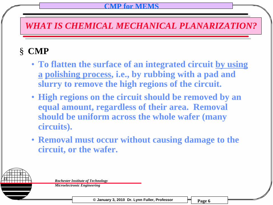
WHAT IS CHEMICAL MECHANICAL PLANARIZATION?
§ CMP• To flatten the surface of an integrated circuit by using
a polishing process, i.e., by rubbing with a pad and slurry to remove the high regions of the circuit.
• High regions on the circuit should be removed by an equal amount, regardless of their area. Removal should be uniform across the whole wafer (many circuits).
• Removal must occur without causing damage to the circuit, or the wafer.

© January 3, 2010 Dr. Lynn Fuller, Professor
CMP for MEMS
Page 7
Rochester Institute of TechnologyMicroelectronic Engineering
WHAT TO WE MEAN, TO“PLANARIZE AN INTEGRATED CIRCUIT”?
Planarization is one or both of the following :
a. Topography smoothing: the conversion of abrupt, vertical steps to gradually sloping transitions.
b. Step height reduction: the reduction of elevation differences
© January 3, 2010 Dr. Lynn Fuller, Professor
CMP for MEMS
Page 8
Rochester Institute of TechnologyMicroelectronic Engineering
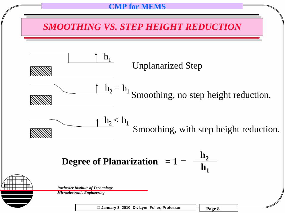
SMOOTHING VS. STEP HEIGHT REDUCTION
h1
h2 = h1
h2 < h1
Unplanarized Step
Smoothing, no step height reduction.
Smoothing, with step height reduction.
Degree of Planarization = 1 _ h2
h1

© January 3, 2010 Dr. Lynn Fuller, Professor
CMP for MEMS
Page 9
Rochester Institute of TechnologyMicroelectronic Engineering
PLANARIZATION RANGE
Global Planarization
Short Range: r =1-2 µm
Long Range: r = 100 - 200 µmθ
r
θ
r
θ = 30 - 45 deg.
θ = 1- 0.01 deg.
Planarization Range (r) = Post-Step Heighttan (θ)

© January 3, 2010 Dr. Lynn Fuller, Professor
CMP for MEMS
Page 10
Rochester Institute of TechnologyMicroelectronic Engineering
WHY DO WE NEED TO PLANARIZE?
Lithography is better with planar surfaces. Higher resolution is possible. Small depth of focus problems can be avoided.
Shallow trench isolation in CMOS processes.
Multilayer metal.
Patterning materials that are hard to etch.
Some MEMS devices will not move unless they are flat. Especially gears and linkages.

© January 3, 2010 Dr. Lynn Fuller, Professor
CMP for MEMS
Page 11
Rochester Institute of TechnologyMicroelectronic Engineering
CANON FPA-2000 i1 STEPPER
i-Line Stepper λ = 365 nmNA = 0.52, σ = 0.6Resolution = 0.7 λ / NA = ~0.5 µm20 x 20 mm Field SizeDepth of Focus = k2 λ/(NA)2

© January 3, 2010 Dr. Lynn Fuller, Professor
CMP for MEMS
Page 12
Rochester Institute of TechnologyMicroelectronic Engineering
RESOLUTION AND DEPTH OF FOCUS
§ Resolvable Linewidth = k1 λ/NA
§ Depth of Focus = k2 λ/(NA)2
λ = exposure wavelength (365 nm) NA = numerical aperture of stepper (0.52) k = constant, whose value depends strongly on the
resist system and type of feature (0.61 theoretical)
§ For resolution of ~0.5 µm, depth of focus is ~0.8 µm, therefore planarization is required.

© January 3, 2010 Dr. Lynn Fuller, Professor
CMP for MEMS
Page 13
Rochester Institute of TechnologyMicroelectronic Engineering
SHALLOW TRENCH ISOLATION (FEOL)
Si3N4
Pad Oxide
Silicon
Si3N4
Pad Oxide
Silicon
Si3N4
Silicon
Pad Oxide
Si3N4
Silicon
Pad Oxide
CVD SiO2
Si3N4
Pad Oxide
CVD SiO2
Silicon
Si3N4
Pad Oxide
CVD SiO2
Silicon
1. Thermal OxidationDeposit Nitride
2. Pattern and etch Nitride and oxide
3. Etch trench in silicon substrate
4. Thermal Oxidation Deposit CVD Oxide
5. CMP of oxide to Nitride polish stop
6. Chemical strip of Nitride
Nitride polish stop and its subsequent removal helps to minimize dishing in trenches.
© January 3, 2010 Dr. Lynn Fuller, Professor
CMP for MEMS
Page 14
Rochester Institute of TechnologyMicroelectronic Engineering
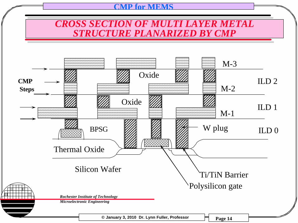
CROSS SECTION OF MULTI LAYER METAL STRUCTURE PLANARIZED BY CMP
CMPSteps
Thermal Oxide
Silicon Wafer
ILD 0
ILD 1
ILD 2
W plug
Oxide
M-1
M-2
M-3
BPSG
Polysilicon gateTi/TiN Barrier
Oxide

© January 3, 2010 Dr. Lynn Fuller, Professor
CMP for MEMS
Page 15
Rochester Institute of TechnologyMicroelectronic Engineering
CMP IN MEMS ALLOWS DEVICES TO MOVE (SPIN)
X and Y movement90° out of phase
X Y
Poly 1 – rotating gearPoly 2 – anchor pin
Poly 3 - linkage
Where is CMP used and why?
Poly 1 – X/Y motion

© January 3, 2010 Dr. Lynn Fuller, Professor
CMP for MEMS
Page 16
Rochester Institute of TechnologyMicroelectronic Engineering
CMOS FIRST MEMS AFTER, TEXAS INSTRUMENTS
TORSIONAL MIRRORS
TI Digital Mirror Array
1 millionMirrors

© January 3, 2010 Dr. Lynn Fuller, Professor
CMP for MEMS
Page 17
Rochester Institute of TechnologyMicroelectronic Engineering
MEMS FIRST CMP THEN CMOS PROCESSING
Buried Polysilicon MEMs with CMP planarizationand CMOS post-fabrication (after Nasby, et al, 1996)

© January 3, 2010 Dr. Lynn Fuller, Professor
CMP for MEMS
Page 18
Rochester Institute of TechnologyMicroelectronic Engineering
WHAT IS PLANARIZED, SPECIFICALLY?
§ Front end Applications (FEOL) - Devices in the active regions of the silicon wafer, such as: Shallow trench isolation (STI) Trench capacitors Inter-polysilicon dielectrics
§ Back end applications (BEOL) - Metal and dielectric films which comprise the wiring of the millions of devices in the silicon wafer. Pre-metal dielectrics (doped oxides, e.g.BPSG, PSG) Lateral and Vertical interconnections (Al, W, Cu, Ta,
Ti, TiN, doped Silicon Cu-alloys, Al-alloys) Intermetal dielectrics (TEOS, SOG, SiO2, BPSG,
PSG, Si3N4 ) Polymers (Polyimide)
© January 3, 2010 Dr. Lynn Fuller, Professor
CMP for MEMS
Page 19
Rochester Institute of TechnologyMicroelectronic Engineering
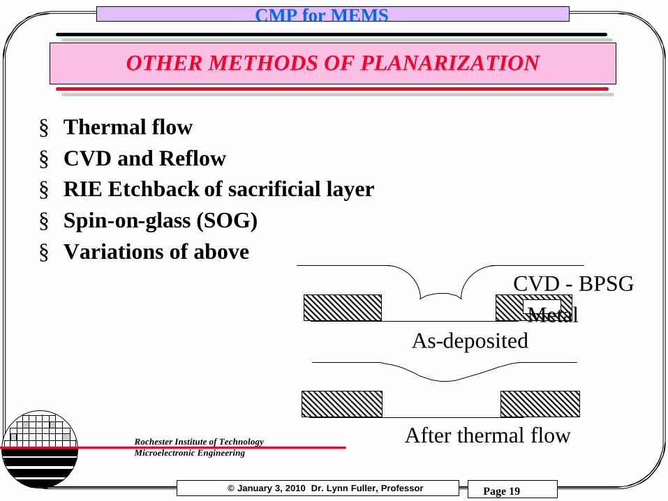
OTHER METHODS OF PLANARIZATION
§ Thermal flow§ CVD and Reflow§ RIE Etchback of sacrificial layer§ Spin-on-glass (SOG)§ Variations of above
As-deposited
After thermal flow
CVD - BPSGMetal
© January 3, 2010 Dr. Lynn Fuller, Professor
CMP for MEMS
Page 20
Rochester Institute of TechnologyMicroelectronic Engineering
WHY IS CMP SO GREAT?
§ It is the only process which can planarize on a global scale.§ Alternative planarization processes are affected by the
pattern size and density.
§ It is an enabling process:§ Maximizes lithographic performance.§ Improves cleaning.§ Reduces yield limiting defects from other processes.§ Permits the use of difficult-to-etch metals such as Cu.

© January 3, 2010 Dr. Lynn Fuller, Professor
CMP for MEMS
Page 21
Rochester Institute of TechnologyMicroelectronic Engineering
WHAT IS LAPPING and POLISHING?
Lapping –To planarize or to create desired shape or dimension.To produce a uniformly abraded surface with known degree
of sub-surface damage (~1/4 of grit size)Slurry of water and 8-micrometer alumina grit.Cast iron lapping plates, double side lapping produces
flatness and parallelism < 2 µm.Typical removal, 50 µm per side.
Polishing –To remove residual damage from lappingTo produce no new damageTo create a microscopically smooth surfaceDoes not change the shape of the surfaceGentle rubbing with a soft pad saturated with polishing
slurry (CeO2, Fe2O3, ZrO2, SiO2). It involves both a chemical and a mechanical component. At pH=10.5

© January 3, 2010 Dr. Lynn Fuller, Professor
CMP for MEMS
Page 22
Rochester Institute of TechnologyMicroelectronic Engineering
WAFER LAPPING ( GRINDING OR THINNING)
Wafers are often thinned before packaging. A thinner wafer allows for better heat removal, lower electrical resistance through the substrate and thinner packages. In MEMS wafer thinning allows for easier formation of thru wafer holes when combined with CMP double sided processing. We have been thinning our MEMS wafers from ~500µm down to ~300µm and then polishing to make thin double sided starting wafers.

© January 3, 2010 Dr. Lynn Fuller, Professor
CMP for MEMS
Page 23
Rochester Institute of TechnologyMicroelectronic Engineering
SILICON POLISHING VS IC PLANARIZATION
Lapped surfaceSubsurface damage
Pad
Device region
Patterned surface,Pad may contact two materials.
Pad
OxideMetal
silicon
Monocrystalline siliconPOLISHING
PLANARIZATION

© January 3, 2010 Dr. Lynn Fuller, Professor
CMP for MEMS
Page 24
Rochester Institute of TechnologyMicroelectronic Engineering
PAD - SLURRY - SURFACE INTERACTION
Wafer
Pad
Oxide/trench fillSlurry
Pad saturated with slurry.Polishing pressure greatest on small, elevated features (active).Pad may contact larger low areas (large field regions) called dishing.
ActiveField or TrenchField or Trench

© January 3, 2010 Dr. Lynn Fuller, Professor
CMP for MEMS
Page 25
Rochester Institute of TechnologyMicroelectronic Engineering
ELECTROMET GRINDING TOOL
Platen Speed = 200 rpmPressure = 40 psiRemoval Rate = ~6 min/100µmTime = 12 minWater On
Grinder Wafer ThicknessMeasurement

© January 3, 2010 Dr. Lynn Fuller, Professor
CMP for MEMS
Page 26
Rochester Institute of TechnologyMicroelectronic Engineering
GRINDING DISK
http://www.grainger.com/Grainger/wwg/productIndex.shtml
Grinding Disk

© January 3, 2010 Dr. Lynn Fuller, Professor
CMP for MEMS
Page 27
Rochester Institute of TechnologyMicroelectronic Engineering
CMP EQUIPMENT SCHEMATIC CONVENTIONAL ORBITAL

© January 3, 2010 Dr. Lynn Fuller, Professor
CMP for MEMS
Page 28
Rochester Institute of TechnologyMicroelectronic Engineering
WESTECH

© January 3, 2010 Dr. Lynn Fuller, Professor
CMP for MEMS
Page 29
Rochester Institute of TechnologyMicroelectronic Engineering
CMP TO OBTAIN OPTICALLY SMOOTH SURFACE
Strassbaugh CMP ToolSlurry: Klebosol 1501-50 Colloidal Silica 5 gal pail $255 each, Mfg AZ Electronic Materials, Clariant’s Klebosolline of silica slurrys, 50nm particles, KOH, pH 10.9, 50% solids or equivalent slurry.
15 min per wafer Slurry drip rate: ~1 drop/secondDown Pressure = 8 psiQuill Speed = 70 rpmOscillation Speed = 6 per minTable Speed = 50 rpm (~10 Hz)
Strassbaugh CMP Tool

© January 3, 2010 Dr. Lynn Fuller, Professor
CMP for MEMS
Page 30
Rochester Institute of TechnologyMicroelectronic Engineering
CMP TOOL MANUFACTURERS
Applied MaterialsCranfield PrecisionEbaraFujikoshiLapmasterMitsubishiNutoolOkimotoPeter WoltersPresiSonySpeedfam/IPECStrasbaughToshiba

© January 3, 2010 Dr. Lynn Fuller, Professor
CMP for MEMS
Page 31
Rochester Institute of TechnologyMicroelectronic Engineering
SLURRY DISTRIBUTION SYSTEMS
EbaraFSIMega SystemsSpeedfam/IPECSystems ChemistryUniversal Photronics

© January 3, 2010 Dr. Lynn Fuller, Professor
CMP for MEMS
Page 32
Rochester Institute of TechnologyMicroelectronic Engineering
POST CMP CLEAN TOOLS
ToolsDai Mippon Screen (DNS)Oliver DesignOnTrak Systems (Lamb)Solid State Equipment Speedfam/IPECSumitomo MetalsToshiba
PVA Brush RollersCupps IndustrialKaneboMerocelSyntaxUniversal Photronics

© January 3, 2010 Dr. Lynn Fuller, Professor
CMP for MEMS
Page 33
Rochester Institute of TechnologyMicroelectronic Engineering
METROLOGY FOR WAFER THICKNESS
Wafer ThicknessMeasurement
Right now we don't have a good way to measure the wafer thickness. Just the mechanical dial micrometer shown. But that shows less than 1 mil (25µm) change across wafer diameter.

© January 3, 2010 Dr. Lynn Fuller, Professor
CMP for MEMS
Page 34
Rochester Institute of TechnologyMicroelectronic Engineering
MECHANICAL STYLIS METROLOGY TOOLS
We used our long scan Tencore P2 profiler to see if that will give us a better idea of the uniformity of these processes.
Surface roughness ~1µm (10,000Å) after grindingAfter polish ~50Å

© January 3, 2010 Dr. Lynn Fuller, Professor
CMP for MEMS
Page 35
Rochester Institute of TechnologyMicroelectronic Engineering
OPTICAL METROLOGY TOOLS
ADEBio-RadMamamatsuHitachiHoribaKLA/TencorMatecNanometricsRudolph InstrumentsSpeedfam/IPECTopcon
WHITE LIGHT SOURCE
OPTICS
WAFER
MONOCHROMATOR& DETECTOR
λ
3000 Å OXIDE

© January 3, 2010 Dr. Lynn Fuller, Professor
CMP for MEMS
Page 36
Rochester Institute of TechnologyMicroelectronic Engineering
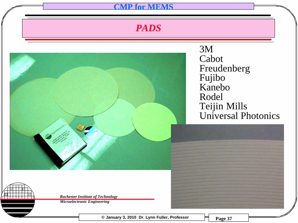
PADS
Impregnated – non woven polyester base, saturated with polyurethane which binds the base together when cured. Pad is abrasively buffed to condition it for use. Range of hardness and densities are available.
Cast – foamed polyurethane is cast in molds and cross-linked, after which it is sliced into sheets from 0.020 to 1.25 inches thickness. A wide range of density and hardness is available.
Coated – a non woven polyester base is coated with a polyurethanteformulation which forms a skin layer which is abrasively buffed before use. Often used as a final cosmetic polish after stock removal with cast or impregnated pads.
© January 3, 2010 Dr. Lynn Fuller, Professor
CMP for MEMS
Page 37
Rochester Institute of TechnologyMicroelectronic Engineering
PADS
3MCabotFreudenbergFujiboKaneboRodelTeijin MillsUniversal Photonics

© January 3, 2010 Dr. Lynn Fuller, Professor
CMP for MEMS
Page 38
Rochester Institute of TechnologyMicroelectronic Engineering
STACKED PAD
Hard top pad Resilient bottom pad
Metal platen
Hard upper pad reduces dishing while compressible lower pad conforms globally to the wafer surface, improving uniformity.

© January 3, 2010 Dr. Lynn Fuller, Professor
CMP for MEMS
Page 39
Rochester Institute of TechnologyMicroelectronic Engineering
PAD CONDITIONING
Purposeto help maintain stability of removal rate in CMPTo maintain long pad lifeTo maintain removal rate uniformity within waferRemoves imbedded and caked debris in pad surfaceExposes uniform pad materialAbrades pad surfaceMaintains planar pad surface
TechniqueA diamond plated disc is applied to the pad using a prescribed downward force and rotation program, in the presence of water

© January 3, 2010 Dr. Lynn Fuller, Professor
CMP for MEMS
Page 40
Rochester Institute of TechnologyMicroelectronic Engineering
SLURRIES
MetalsColloidal alumina and ferric nitrate, low pH
Weak oxide film is formed using MnO2 based polishing agent, which is removed with MnO2 mechanical action.
OxidesColloidal Silica (sub micron particle size) in water with KOH or NH4OH, pH of 10.5
Cerium Oxide CeO2 (sub micron particle size), High PhZirconium oxide

© January 3, 2010 Dr. Lynn Fuller, Professor
CMP for MEMS
Page 41
Rochester Institute of TechnologyMicroelectronic Engineering
SLURRY MANUFACTURERS
CabotEKC TechnologiesFujimiIntersurface DynamicsPraxairRodelTranselco/FerroUniversal Photonics

© January 3, 2010 Dr. Lynn Fuller, Professor
CMP for MEMS
Page 42
Rochester Institute of TechnologyMicroelectronic Engineering
COMPARISON BETWEEN OLD CMP SLURRY AND PROCESS AND NEW SLURRY AND PROCESS
Wafer before CMP
Old Process and Slurry
After 9.5 minutes of PolishingCenter done, Edges Bare
After 5 minutes of PolishingCenter not done
After 2.25 minutes of PolishingClear almost every die
Even edge die
New Process and Slurry

© January 3, 2010 Dr. Lynn Fuller, Professor
CMP for MEMS
Page 43
Rochester Institute of TechnologyMicroelectronic Engineering
NEW RIT CMOS FACTORY STI PROCESS
§ Carrier speed: 30 RPM§ Platen speed: 100 RPM§ Without back pressure§ 8 PSI down force (36 PSI on the gauge)§ Slurry (made for STI, see pages below)§ Slurry flow rate (60 mL/min)§ Pad conditioning: before every run§ Temperature: 80°C§ Polishing time: 2min 30 sec for 6500A oxide
Peng Xie and Mike Aquilino
© January 3, 2010 Dr. Lynn Fuller, Professor
CMP for MEMS
Page 44
Rochester Institute of TechnologyMicroelectronic Engineering
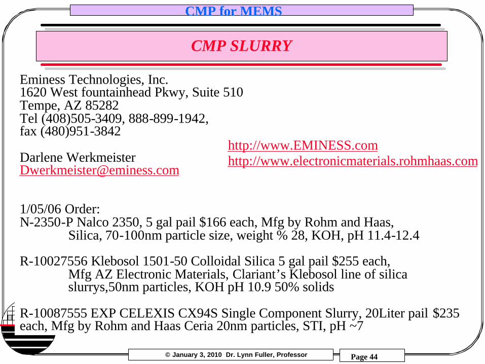
CMP SLURRY
Eminess Technologies, Inc.1620 West fountainhead Pkwy, Suite 510Tempe, AZ 85282Tel (408)505-3409, 888-899-1942, fax (480)951-3842
Darlene [email protected]
1/05/06 Order:N-2350-P Nalco 2350, 5 gal pail $166 each, Mfg by Rohm and Haas,
Silica, 70-100nm particle size, weight % 28, KOH, pH 11.4-12.4
R-10027556 Klebosol 1501-50 Colloidal Silica 5 gal pail $255 each, Mfg AZ Electronic Materials, Clariant’s Klebosol line of silica slurrys,50nm particles, KOH pH 10.9 50% solids
R-10087555 EXP CELEXIS CX94S Single Component Slurry, 20Liter pail $235 each, Mfg by Rohm and Haas Ceria 20nm particles, STI, pH ~7
http://www.EMINESS.comhttp://www.electronicmaterials.rohmhaas.com

© January 3, 2010 Dr. Lynn Fuller, Professor
CMP for MEMS
Page 45
Rochester Institute of TechnologyMicroelectronic Engineering
CONVENTIONAL PROCESSING TECHNOLOGYFOR MULTILEVEL METALLIZATION
Previous metal lines
Previous metal vias
Deposit and pattern metal for via plugs
Deposit insulating film
CMP insulating film
1.
2.
3.
4.
5. Repeat steps 2-5 for next level (metal lines)

© January 3, 2010 Dr. Lynn Fuller, Professor
CMP for MEMS
Page 46
Rochester Institute of TechnologyMicroelectronic Engineering
INLAID METAL (DAMASCENE) TECHNOLOGY
Previous metal vias1.Previous metal lines
Deposit Dielectric and etch vias
Deposit blanket metal
CMP metal
2.
3.
4.
5. Repeat steps 2-5 for next level of metal lines.

© January 3, 2010 Dr. Lynn Fuller, Professor
CMP for MEMS
Page 47
Rochester Institute of TechnologyMicroelectronic Engineering
DUAL INLAID METAL (DUAL DAMASCENE)
Insulator: thk. = stud height
Si-Nitrideetch stop
Insulator:thk. = interconnect
Resist
Si-Nitrideetch stop
Insulator:thk. = interconnect
1. Deposit insulator, cap with nitride etch stop.Pattern nitride for studs, deposit second layerof insulator, apply resist.
2. Etch insulator down to substrate, strip resist.
3. Deposit metal, filling all features.
4. CMP of metal, stop at dielectric.
Insulator: thk. = stud height
Dual approach requires 20-30% fewer steps than traditional subtractive patterning.
SubstrateSubstrate
Substrate Substrate
Cu or Al

© January 3, 2010 Dr. Lynn Fuller, Professor
CMP for MEMS
Page 48
Rochester Institute of TechnologyMicroelectronic Engineering
METAL POLISHING
• Corrosion of the metal by the slurry (chemical)• Passivation (self-limiting corrosion due to surface
protective layer, usually oxide)• Removal of the passivation from the high regions,
from the action of the pad/slurry attrition.• Reformation of the passivation layer on the
exposed metal surfaces.

© January 3, 2010 Dr. Lynn Fuller, Professor
CMP for MEMS
Page 49
Rochester Institute of TechnologyMicroelectronic Engineering
Cu INTERCONNECT
© January 3, 2010 Dr. Lynn Fuller, Professor
CMP for MEMS
Page 50
Rochester Institute of TechnologyMicroelectronic Engineering
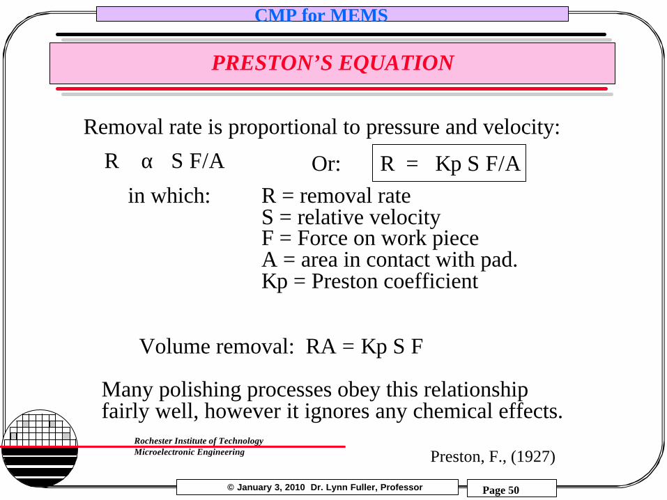
PRESTON’S EQUATION
Removal rate is proportional to pressure and velocity:
R α S F/A Or: R = Kp S F/Ain which: R = removal rate
S = relative velocityF = Force on work pieceA = area in contact with pad.Kp = Preston coefficient
Many polishing processes obey this relationship fairly well, however it ignores any chemical effects.
Preston, F., (1927)
Volume removal: RA = Kp S F

© January 3, 2010 Dr. Lynn Fuller, Professor
CMP for MEMS
Page 51
Rochester Institute of TechnologyMicroelectronic Engineering
POLISH RATE VS. PATTERN DENSITY
Blanket Polishing
Pad
Wafer
Patterned polishing. No pad contact between features
Area = Wafer area
Area = pattern area
Area = ?
Patterned polishing. Some pad contact between features.
Volumetric rate: RA = Kp F S

© January 3, 2010 Dr. Lynn Fuller, Professor
CMP for MEMS
Page 52
Rochester Institute of TechnologyMicroelectronic Engineering
SHALLOW TRENCH ISOLATION CMP
We have made great progress in doing the CMP for our advanced CMOS process shallow trench isolation (STI). The progress has been made through:
1. Getting the Westech CMP tool working correctly.2. Getting a slurry especially made for STI that removes
oxide and stops on nitride.3. Adding tiles (dummy features) to the mask area outside
of the active regions during computer aided transcription CATS prior to maskmaking.

© January 3, 2010 Dr. Lynn Fuller, Professor
CMP for MEMS
Page 53
Rochester Institute of TechnologyMicroelectronic Engineering
DISHING AND TILES
Wafer
Field Oxide, Filled Trench
Active
Dishing: large area becomes recessedespecially with over polishing
Multiple small dummy features (tiles) are used to reduce Dishing.

© January 3, 2010 Dr. Lynn Fuller, Professor
CMP for MEMS
Page 54
Rochester Institute of TechnologyMicroelectronic Engineering
TILING FOR STI LAYER MASKMAKING
Synopsys, Inc.CATS Software for transcription of CAD design files into readable e-beam and laser formats.

RIT ADVANCED CMOS PROCESS
11 PHOTOLEVELS
POLY
METAL
N-WELL
P SELECTCC
ACTIVE
N SELECT
LVL 2 - NWell
LVL 3 - Pwell
LVL 5 - POLY
LVL 7 - NLDD
LVL 10 - CC
LVL 11 – METAL 1
LVL 8 – N+D/S
LVL 9 – P+D/S
LVL 6 - PLDD
LVL 4 - VTP
NMOSFET PMOSFET
N-wellP-well
N+ Poly
P+ D/SN+ D/S
LDDLDD
n+ wellcontact
p+ wellcontact
P+ PolyLVL 1 - STI

© January 3, 2010 Dr. Lynn Fuller, Professor
CMP for MEMS
Page 56
Rochester Institute of TechnologyMicroelectronic Engineering
PARAMETERS THAT AFFECT REMOVAL RATE
Slurry ChemicalspHBuffering agentsoxidizerscomplexing agentsconcentrationdielectric constant
Slurry AbrasivetypesizeconcentrationpHsuspension stability
Slurry Flow RateFilms being PolishedTemperature
(5X removal rate/ 20 °C)
Downward PressurePlaten SpeedCarrier SpeedPattern Geometries
Feature SizePattern Density
Pad Typefiber structurepore sizehardnesselastic and shear modulusthicknessembossing or perforationsconditioningaging effectschemical durability
Wafer size

© January 3, 2010 Dr. Lynn Fuller, Professor
CMP for MEMS
Page 57
Rochester Institute of TechnologyMicroelectronic Engineering
CHANGE AND EFFECT
Increase pressure – increase removal rate, degrade surface finishIncrease carrier speed – increase removal rate, degrade uniformityIncrease platen speed – increase removal rate, degrade uniformityIncrease slurry flow – decrease removal rate, improve surface finish
© January 3, 2010 Dr. Lynn Fuller, Professor
CMP for MEMS
Page 58
Rochester Institute of TechnologyMicroelectronic Engineering
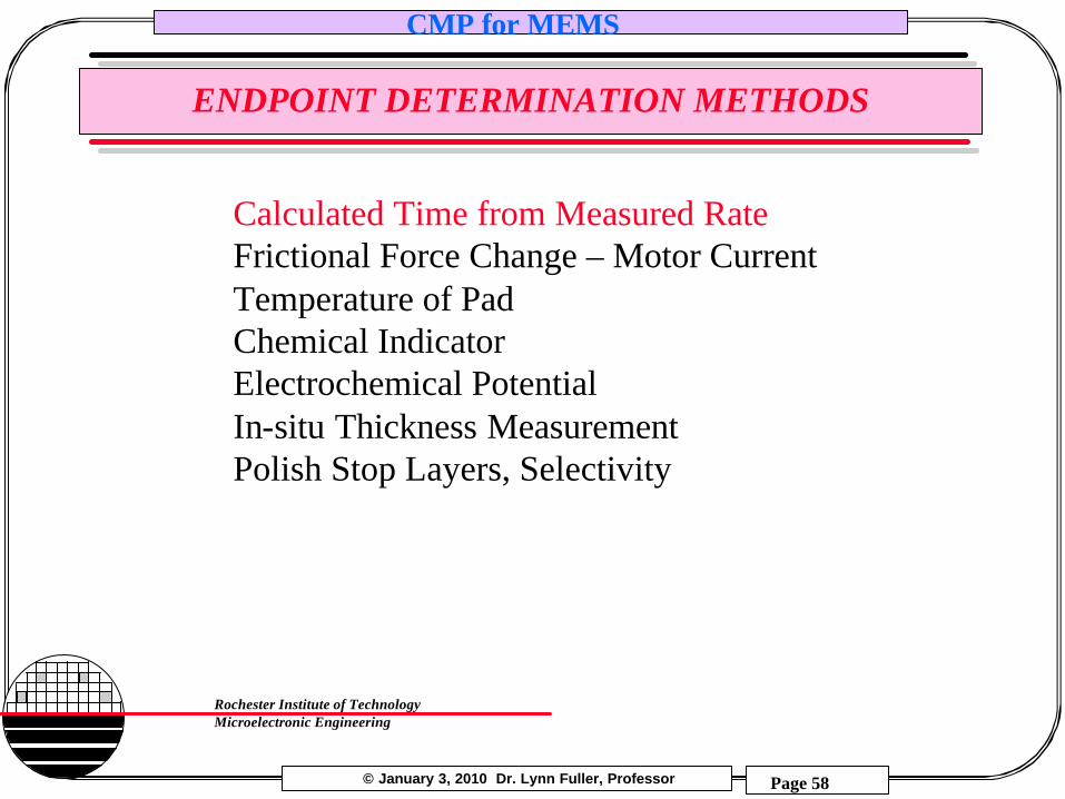
ENDPOINT DETERMINATION METHODS
Calculated Time from Measured RateFrictional Force Change – Motor CurrentTemperature of PadChemical IndicatorElectrochemical PotentialIn-situ Thickness MeasurementPolish Stop Layers, Selectivity

© January 3, 2010 Dr. Lynn Fuller, Professor
CMP for MEMS
Page 59
Rochester Institute of TechnologyMicroelectronic Engineering
SUMMARY
§ CMP is widely accepted now, after the industry overcame the old paradigm of always keeping the wafer clean.
§ CMP adds cost, ($7-10 per wafer) but its ability to enhance other processing steps while improving circuit performance results in a significant overall benefit.

© January 3, 2010 Dr. Lynn Fuller, Professor
CMP for MEMS
Page 60
Rochester Institute of TechnologyMicroelectronic Engineering
REFERENCES
1. Sivaram, et.al., Solid State Technology, May, p87, 1992.2. Wilson, S. R., et.al., Handbook of Multilevel Metallization,
Noyes, Park Ridge, NJ, 1993. 3. Pangrie, S. K., et.al., Proceedings of CMP-VMIC Conference,
Santa Clara, CA, Feb 22-23, p47, 1996.4. Sethuraman, A.R., et.al., J. Electronic Materials, vol 25, No.10,
1996.5. Warnock, J.J., Electrochemical Soc., 138, No.11, p3460-65, 1991.6. Litvak, H.E., US Patent No. 5,449,733 issued March 19, 1996.7. Pietsch, G.J., et.al., Journal Applied Physics, 34, p6311, 1995.8. Synopsys, Inc, CATS user guide, Y-2006.09, September 2006.

© January 3, 2010 Dr. Lynn Fuller, Professor
CMP for MEMS
Page 61
Rochester Institute of TechnologyMicroelectronic Engineering
HOMEWORK - CMP
Visit your CMP area or interview a CMP expert and determine:1. Type of equipment used.2. How endpoint is determined.3. What pads and slurry are used.4. When are the pads replaced.5. What different processes are done. (e.g. what is different
when CMP oxide, CMP metal, etc.)


![Evaluation of Chemical Mechanical Planarization Capability …1095703/...narization (CMP) has evolved into an extensively used technique to achieve the aforementioned planarity [1,2,3,4]](https://img.pdfslide.us/doc/110x75/6126add663fea728774def08/evaluation-of-chemical-mechanical-planarization-capability-1095703-narization.jpg)