Embed Size (px)
Citation preview
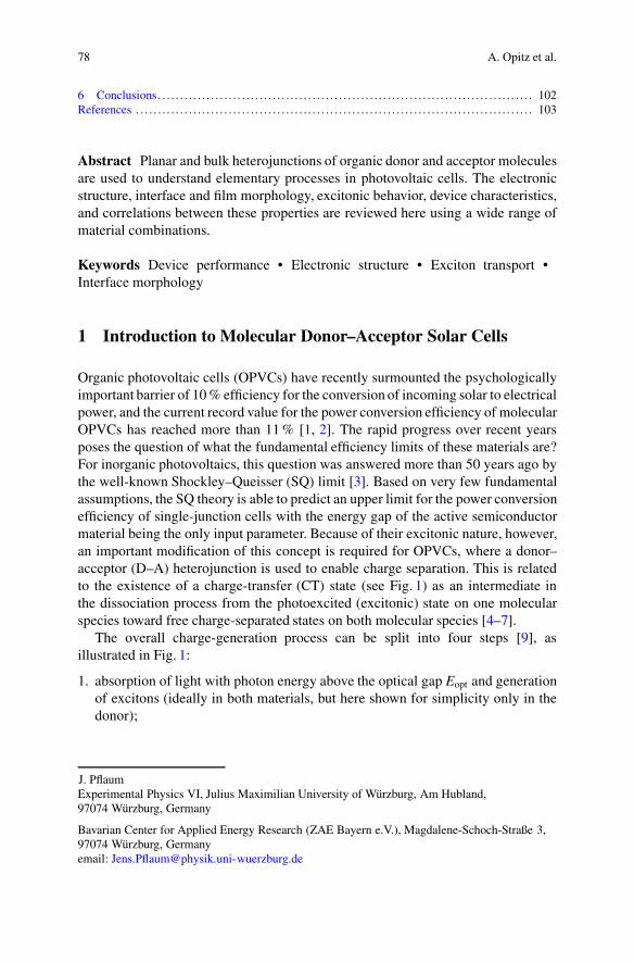
Charge Separation at Nanostructured MolecularDonor–Acceptor Interfaces
Andreas Opitz, Rupak Banerjee, Stefan Grob, Mark Gruber,Alexander Hinderhofer, Ulrich Hörmann, Julia Kraus, Theresa Linderl,Christopher Lorch, Andreas Steindamm, Anna Katharina Topczak,Andreas Wilke, Norbert Koch, Jens Pflaum, Frank Schreiber,and Wolfgang Brütting
Contents
1 Introduction to Molecular Donor–Acceptor Solar Cells . . . . . . . . . . . . . . . . . . . . . . . . . . . . . . . . . . . . . 782 Electronic Structure . . . . . . . . . . . . . . . . . . . . . . . . . . . . . . . . . . . . . . . . . . . . . . . . . . . . . . . . . . . . . . . . . . . . . . . . . . . . 843 Interface Morphology and Mixing Behavior. . . . . . . . . . . . . . . . . . . . . . . . . . . . . . . . . . . . . . . . . . . . . . . . . . 88
3.1 Interface in PHJ Geometries . . . . . . . . . . . . . . . . . . . . . . . . . . . . . . . . . . . . . . . . . . . . . . . . . . . . . . . . . . . . . 893.2 Phase Separation in BHJ Geometries . . . . . . . . . . . . . . . . . . . . . . . . . . . . . . . . . . . . . . . . . . . . . . . . . . . 90
4 Exciton Diffusion and Dissociation . . . . . . . . . . . . . . . . . . . . . . . . . . . . . . . . . . . . . . . . . . . . . . . . . . . . . . . . . . . 935 Charge Transport and Device Performance . . . . . . . . . . . . . . . . . . . . . . . . . . . . . . . . . . . . . . . . . . . . . . . . . . . 98
A. Opitz (�) • A. WilkeDepartment of Physics, Humboldt-Universität zu Berlin, Newtonstraße 15, 12489 Berlin,Germanye-mail: [email protected]
N. KochDepartment of Physics, Humboldt-Universität zu Berlin, Newtonstraße 15, 12489 Berlin,Germany
Helmholtz-Zentrum Berlin für Materialien und Energie GmbH, Albert-Einstein-Straße 15, 12489Berlin, Germanye-mail: [email protected]
R. Banerjee • A. Hinderhofer • C. Lorch • F. SchreiberInstitut für Angewandte Physik, Eberhard-Karls Universität Tübingen, Auf der Morgenstelle 10,72076 Tübingen, Germanye-mail: [email protected]
S. Grob • M. Gruber • U. Hörmann • J. Kraus • T. Linderl • W. BrüttingInstitute of Physics, University of Augsburg, Universitätsstraße 1, 86135 Augsburg, Germanye-mail: [email protected]
A. Steindamm • A.K. TopczakExperimental Physics VI, Julius Maximilian University of Würzburg, Am Hubland, 97074Würzburg, Germany
© Springer International Publishing Switzerland 2017K. Leo (ed.), Elementary Processes in Organic Photovoltaics,Advances in Polymer Science 272, DOI 10.1007/978-3-319-28338-8_4
77
78 A. Opitz et al.
6 Conclusions. . . . . . . . . . . . . . . . . . . . . . . . . . . . . . . . . . . . . . . . . . . . . . . . . . . . . . . . . . . . . . . . . . . . . . . . . . . . . . . . . . . . . 102References . . . . . . . . . . . . . . . . . . . . . . . . . . . . . . . . . . . . . . . . . . . . . . . . . . . . . . . . . . . . . . . . . . . . . . . . . . . . . . . . . . . . . . . . . . 103
Abstract Planar and bulk heterojunctions of organic donor and acceptor moleculesare used to understand elementary processes in photovoltaic cells. The electronicstructure, interface and film morphology, excitonic behavior, device characteristics,and correlations between these properties are reviewed here using a wide range ofmaterial combinations.
Keywords Device performance • Electronic structure • Exciton transport •Interface morphology
1 Introduction to Molecular Donor–Acceptor Solar Cells
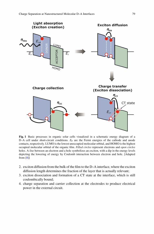
Organic photovoltaic cells (OPVCs) have recently surmounted the psychologicallyimportant barrier of 10 % efficiency for the conversion of incoming solar to electricalpower, and the current record value for the power conversion efficiency of molecularOPVCs has reached more than 11 % [1, 2]. The rapid progress over recent yearsposes the question of what the fundamental efficiency limits of these materials are?For inorganic photovoltaics, this question was answered more than 50 years ago bythe well-known Shockley–Queisser (SQ) limit [3]. Based on very few fundamentalassumptions, the SQ theory is able to predict an upper limit for the power conversionefficiency of single-junction cells with the energy gap of the active semiconductormaterial being the only input parameter. Because of their excitonic nature, however,an important modification of this concept is required for OPVCs, where a donor–acceptor (D–A) heterojunction is used to enable charge separation. This is relatedto the existence of a charge-transfer (CT) state (see Fig. 1) as an intermediate inthe dissociation process from the photoexcited (excitonic) state on one molecularspecies toward free charge-separated states on both molecular species [4–7].
The overall charge-generation process can be split into four steps [9], asillustrated in Fig. 1:
1. absorption of light with photon energy above the optical gap Eopt and generationof excitons (ideally in both materials, but here shown for simplicity only in thedonor);
J. PflaumExperimental Physics VI, Julius Maximilian University of Würzburg, Am Hubland,97074 Würzburg, Germany
Bavarian Center for Applied Energy Research (ZAE Bayern e.V.), Magdalene-Schoch-Straße 3,97074 Würzburg, Germanyemail: [email protected]
Charge Separation at Nanostructured Molecular D–A Interfaces 79
Fig. 1 Basic processes in organic solar cells visualized in a schematic energy diagram of aD–A cell under short-circuit conditions. EF are the Fermi energies of the cathode and anodecontacts, respectively. LUMO is the lowest unoccupied molecular orbital, and HOMO is the highestoccupied molecular orbital of the organic film. Filled circles represent electrons and open circlesholes. A line between an electron and a hole symbolizes an exciton, with a dip in the energy levelsdepicting the lowering of energy by Coulomb interaction between electron and hole. [Adaptedfrom [8]]
2. exciton diffusion from the bulk of the film to the D–A interface, where the excitondiffusion length determines the fraction of the layer that is actually relevant;
3. exciton dissociation and formation of a CT state at the interface, which is stillcoulombically bound;
4. charge separation and carrier collection at the electrodes to produce electricalpower in the external circuit.
80 A. Opitz et al.
Accordingly, the internal quantum efficiency is given by [9]
�int D �Abs � �ED � �CT � �CC ; (1)
which is the product of the absorption efficiency �Abs, the exciton diffusionefficiency �ED, the CT efficiency �CT, and the charge-collection efficiency �CC.
If reflection losses for coupling light into the cell are taken into account, oneobtains the external quantum efficiency (EQE), which is basically the number ofcollected electrons with respect to the number of incident photons,
�ext D .1 � R/ � �int; (2)
with R being the reflectivity of the device. �ext is experimentally determined by themeasured current density at short-circuit conditions divided by the incident lightintensity at a given wavelength and is also termed the incident photon-to-currentefficiency (IPCE).
The overall power conversion efficiency of a solar cell is given by
�P D JSC � VOC � FF
Pin; (3)
where JSC is the short-circuit current density, VOC is the open-circuit voltage, FFis the fill factor, and Pin is the incident optical power density, preferably measuredunder AM1.5 sunlight conditions.
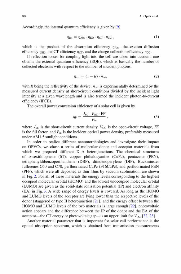
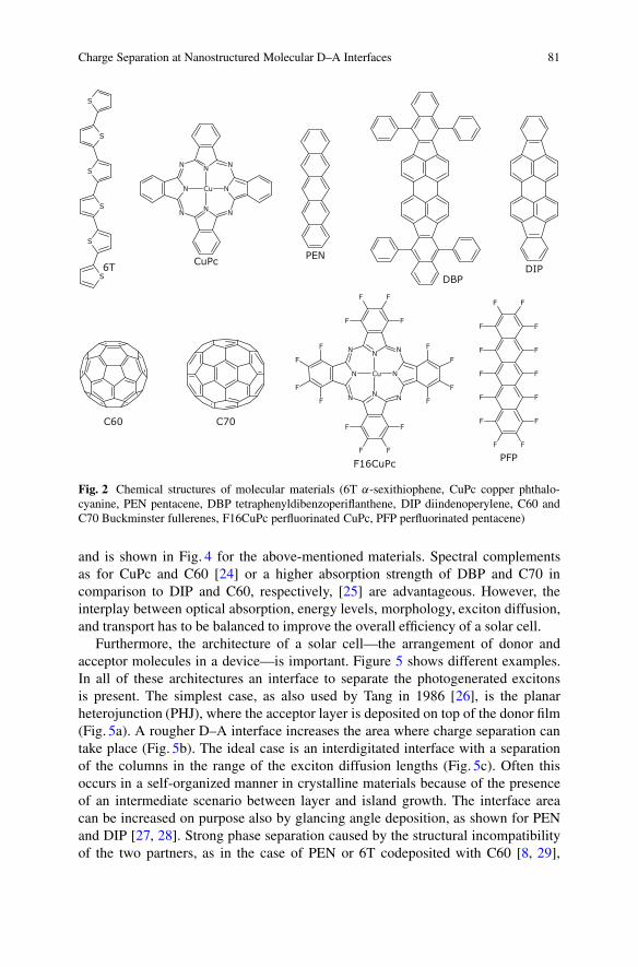
In order to realize different nanomorphologies and investigate their impacton OPVCs, we chose a series of molecular donor and acceptor materials fromwhich we prepared different D–A heterojunctions. The chemical structuresof ˛-sexithiophene (6T), copper phthalocyanine (CuPc), pentacene (PEN),tetraphenyldibenzoperiflanthene (DBP), diindenoperylene (DIP), Buckminsterfullerenes C60 and C70, perfluorinated CuPc (F16CuPc), and perfluorinated PEN(PFP), which were all deposited as thin films by vacuum sublimation, are shownin Fig. 2. For all of these materials the energy levels corresponding to the highestoccupied molecular orbital (HOMO) and the lowest unoccupied molecular orbital(LUMO) are given as the solid-state ionization potential (IP) and electron affinity(EA) in Fig. 3. A wide range of energy levels is covered. As long as the HOMOand LUMO levels of the acceptor are lying lower than the respective levels of thedonor (staggered or type II heterojunction [21]) and the energy offset between theHOMO and LUMO levels of the two materials is large enough [22], photovoltaicaction appears and the difference between the IP of the donor and the EA of theacceptor—the CT energy or photovoltaic gap—is an upper limit for VOC [22, 23].
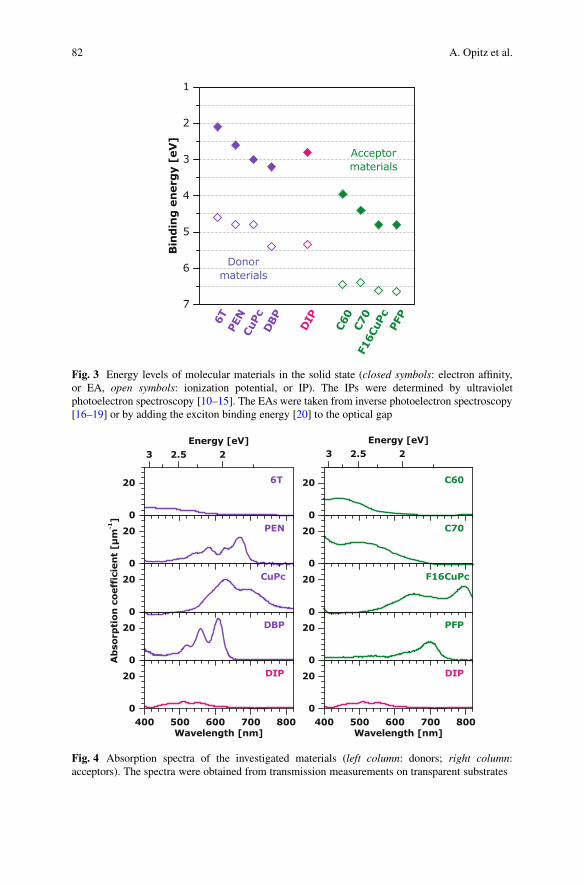
Another material parameter that is important for solar cell performance is theoptical absorption spectrum, which is obtained from transmission measurements
Charge Separation at Nanostructured Molecular D–A Interfaces 81
Fig. 2 Chemical structures of molecular materials (6T ˛-sexithiophene, CuPc copper phthalo-cyanine, PEN pentacene, DBP tetraphenyldibenzoperiflanthene, DIP diindenoperylene, C60 andC70 Buckminster fullerenes, F16CuPc perfluorinated CuPc, PFP perfluorinated pentacene)
and is shown in Fig. 4 for the above-mentioned materials. Spectral complementsas for CuPc and C60 [24] or a higher absorption strength of DBP and C70 incomparison to DIP and C60, respectively, [25] are advantageous. However, theinterplay between optical absorption, energy levels, morphology, exciton diffusion,and transport has to be balanced to improve the overall efficiency of a solar cell.
Furthermore, the architecture of a solar cell—the arrangement of donor andacceptor molecules in a device—is important. Figure 5 shows different examples.In all of these architectures an interface to separate the photogenerated excitonsis present. The simplest case, as also used by Tang in 1986 [26], is the planarheterojunction (PHJ), where the acceptor layer is deposited on top of the donor film(Fig. 5a). A rougher D–A interface increases the area where charge separation cantake place (Fig. 5b). The ideal case is an interdigitated interface with a separationof the columns in the range of the exciton diffusion lengths (Fig. 5c). Often thisoccurs in a self-organized manner in crystalline materials because of the presenceof an intermediate scenario between layer and island growth. The interface areacan be increased on purpose also by glancing angle deposition, as shown for PENand DIP [27, 28]. Strong phase separation caused by the structural incompatibilityof the two partners, as in the case of PEN or 6T codeposited with C60 [8, 29],
82 A. Opitz et al.
Fig. 3 Energy levels of molecular materials in the solid state (closed symbols: electron affinity,or EA, open symbols: ionization potential, or IP). The IPs were determined by ultravioletphotoelectron spectroscopy [10–15]. The EAs were taken from inverse photoelectron spectroscopy[16–19] or by adding the exciton binding energy [20] to the optical gap
Fig. 4 Absorption spectra of the investigated materials (left column: donors; right column:acceptors). The spectra were obtained from transmission measurements on transparent substrates
Charge Separation at Nanostructured Molecular D–A Interfaces 83
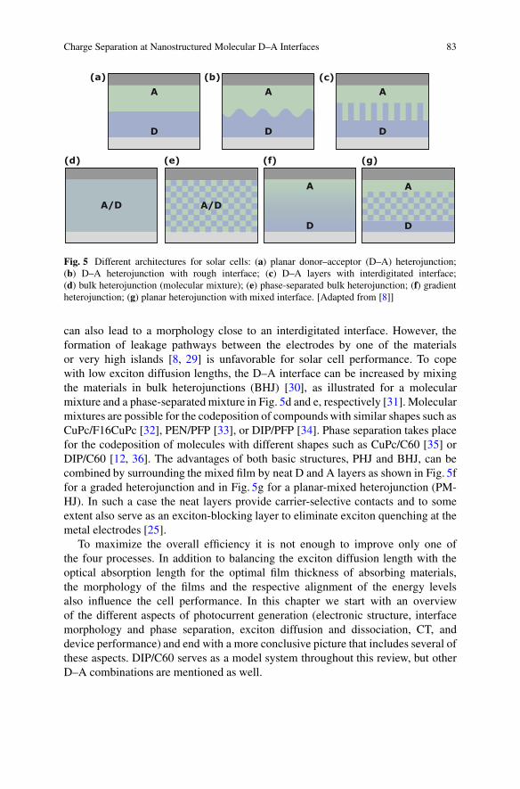
Fig. 5 Different architectures for solar cells: (a) planar donor–acceptor (D–A) heterojunction;(b) D–A heterojunction with rough interface; (c) D–A layers with interdigitated interface;(d) bulk heterojunction (molecular mixture); (e) phase-separated bulk heterojunction; (f) gradientheterojunction; (g) planar heterojunction with mixed interface. [Adapted from [8]]
can also lead to a morphology close to an interdigitated interface. However, theformation of leakage pathways between the electrodes by one of the materialsor very high islands [8, 29] is unfavorable for solar cell performance. To copewith low exciton diffusion lengths, the D–A interface can be increased by mixingthe materials in bulk heterojunctions (BHJ) [30], as illustrated for a molecularmixture and a phase-separated mixture in Fig. 5d and e, respectively [31]. Molecularmixtures are possible for the codeposition of compounds with similar shapes such asCuPc/F16CuPc [32], PEN/PFP [33], or DIP/PFP [34]. Phase separation takes placefor the codeposition of molecules with different shapes such as CuPc/C60 [35] orDIP/C60 [12, 36]. The advantages of both basic structures, PHJ and BHJ, can becombined by surrounding the mixed film by neat D and A layers as shown in Fig. 5ffor a graded heterojunction and in Fig. 5g for a planar-mixed heterojunction (PM-HJ). In such a case the neat layers provide carrier-selective contacts and to someextent also serve as an exciton-blocking layer to eliminate exciton quenching at themetal electrodes [25].
To maximize the overall efficiency it is not enough to improve only one ofthe four processes. In addition to balancing the exciton diffusion length with theoptical absorption length for the optimal film thickness of absorbing materials,the morphology of the films and the respective alignment of the energy levelsalso influence the cell performance. In this chapter we start with an overviewof the different aspects of photocurrent generation (electronic structure, interfacemorphology and phase separation, exciton diffusion and dissociation, CT, anddevice performance) and end with a more conclusive picture that includes several ofthese aspects. DIP/C60 serves as a model system throughout this review, but otherD–A combinations are mentioned as well.
84 A. Opitz et al.
2 Electronic Structure
Ultraviolet and inverse photoelectron spectroscopy (UPS, IPES) were used todetermine the electronic structure of interfaces in our OPVCs. These techniquesassess the distribution of occupied or unoccupied states of the samples [16, 37–41]. Typically, a stepwise deposition enables the investigation of the underlyingfilm, the interface as it is being formed, and the film on top as in PHJs. In recentyears, challenges of this procedure have been highlighted as well[14, 42]. Due tothe different electrostatic potentials of the individual layers of the films and the in-plane electrostatics of the surface, the properties of the interface buried under a toplayer vary from those observed in the experiment when the interface is incrementallybuilt up. Even more complexity occurs if the top-deposited film forms islandsinstead of closed layers, for the same reasons. The combination of electrostaticsimulations [42] and measurements of energy levels lead to an improved and reliableunderstanding of the energy-level alignment at heterojunctions [43, 44]. Further-more, the detrimental effects of the measurement itself have to be considered. Thebombardment of organic materials either with UV photons or with low-energyelectrons can induce damage to the molecules and thus leads to irreversible changesof the energy-level alignment [14].
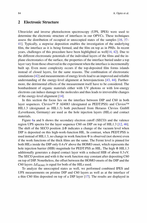
In this section the focus lies on the interface between DIP and C60 in bothlayer sequences. Clevios™ P AI4083 (designated as PEDT:PSS) and Clevios™HIL1.3 (designated as HIL1.3) both purchased from Heraeus Clevios GmbH(Leverkusen, Germany) are used as the hole injection layers (HILs) and contactmaterials.
Figure 6a and b shows the secondary electron cutoff (SECO) and the valenceregion UPS spectra for the layer sequence C60 on DIP on top of HIL1.3 [12, 46].The shift of the SECO position �ˆ indicates a change of the vacuum level whenDIP is deposited on this high-work-function HIL. In contrast, when PEDT:PSS isused instead of HIL1.3, no change in work function ˆ is observed (not shown) evenif the work functions of the thick films are the same. The Fermi level is pinned forboth HILs inside the DIP only 0.4 eV above the HOMO onset, which represents thehole injection barrier (HIB) magnitude for PEDT:PSS as HIL. The high ˆ HIL1.3additionally generates a doped contact layer with a reduced HIB of about 0.3 eV.The SECO position and with it the work function stay constant after depositing C60on top of DIP. Nonetheless, the offset between the HOMO onsets of the DIP and theC60 layers �EHOMO is equal for both of the HILs used.
To analyze the unoccupied states as well, we performed combined IPES andUPS measurements on pristine DIP and C60 layers as well as at the interface ofa thin C60 film deposited on top of a DIP layer [17]. The results are displayed in
Charge Separation at Nanostructured Molecular D–A Interfaces 85
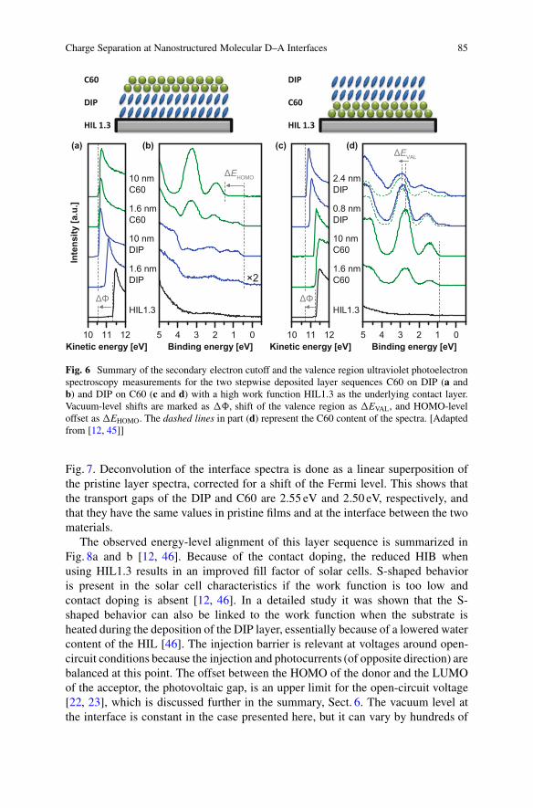
Fig. 6 Summary of the secondary electron cutoff and the valence region ultraviolet photoelectronspectroscopy measurements for the two stepwise deposited layer sequences C60 on DIP (a andb) and DIP on C60 (c and d) with a high work function HIL1.3 as the underlying contact layer.Vacuum-level shifts are marked as �ˆ, shift of the valence region as �EVAL, and HOMO-leveloffset as �EHOMO. The dashed lines in part (d) represent the C60 content of the spectra. [Adaptedfrom [12, 45]]
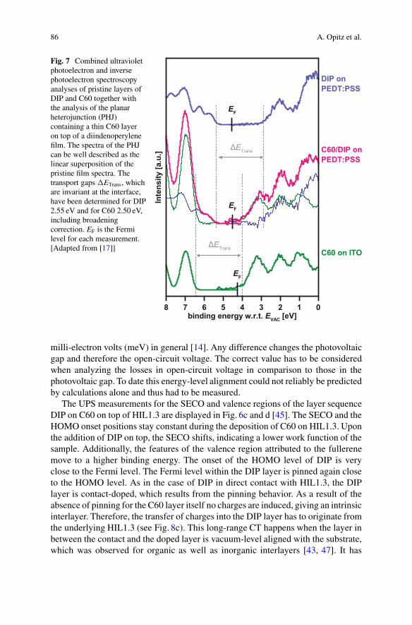
Fig. 7. Deconvolution of the interface spectra is done as a linear superposition ofthe pristine layer spectra, corrected for a shift of the Fermi level. This shows thatthe transport gaps of the DIP and C60 are 2.55 eV and 2.50 eV, respectively, andthat they have the same values in pristine films and at the interface between the twomaterials.
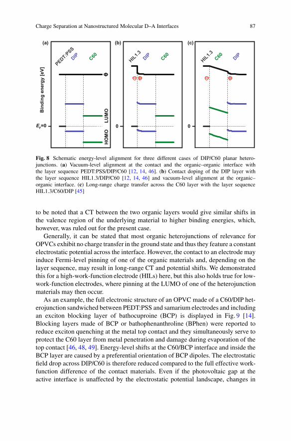
The observed energy-level alignment of this layer sequence is summarized inFig. 8a and b [12, 46]. Because of the contact doping, the reduced HIB whenusing HIL1.3 results in an improved fill factor of solar cells. S-shaped behavioris present in the solar cell characteristics if the work function is too low andcontact doping is absent [12, 46]. In a detailed study it was shown that the S-shaped behavior can also be linked to the work function when the substrate isheated during the deposition of the DIP layer, essentially because of a lowered watercontent of the HIL [46]. The injection barrier is relevant at voltages around open-circuit conditions because the injection and photocurrents (of opposite direction) arebalanced at this point. The offset between the HOMO of the donor and the LUMOof the acceptor, the photovoltaic gap, is an upper limit for the open-circuit voltage[22, 23], which is discussed further in the summary, Sect. 6. The vacuum level atthe interface is constant in the case presented here, but it can vary by hundreds of
86 A. Opitz et al.
Fig. 7 Combined ultravioletphotoelectron and inversephotoelectron spectroscopyanalyses of pristine layers ofDIP and C60 together withthe analysis of the planarheterojunction (PHJ)containing a thin C60 layeron top of a diindenoperylenefilm. The spectra of the PHJcan be well described as thelinear superposition of thepristine film spectra. Thetransport gaps �ETrans, whichare invariant at the interface,have been determined for DIP2.55 eV and for C60 2.50 eV,including broadeningcorrection. EF is the Fermilevel for each measurement.[Adapted from [17]]
milli-electron volts (meV) in general [14]. Any difference changes the photovoltaicgap and therefore the open-circuit voltage. The correct value has to be consideredwhen analyzing the losses in open-circuit voltage in comparison to those in thephotovoltaic gap. To date this energy-level alignment could not reliably be predictedby calculations alone and thus had to be measured.
The UPS measurements for the SECO and valence regions of the layer sequenceDIP on C60 on top of HIL1.3 are displayed in Fig. 6c and d [45]. The SECO and theHOMO onset positions stay constant during the deposition of C60 on HIL1.3. Uponthe addition of DIP on top, the SECO shifts, indicating a lower work function of thesample. Additionally, the features of the valence region attributed to the fullerenemove to a higher binding energy. The onset of the HOMO level of DIP is veryclose to the Fermi level. The Fermi level within the DIP layer is pinned again closeto the HOMO level. As in the case of DIP in direct contact with HIL1.3, the DIPlayer is contact-doped, which results from the pinning behavior. As a result of theabsence of pinning for the C60 layer itself no charges are induced, giving an intrinsicinterlayer. Therefore, the transfer of charges into the DIP layer has to originate fromthe underlying HIL1.3 (see Fig. 8c). This long-range CT happens when the layer inbetween the contact and the doped layer is vacuum-level aligned with the substrate,which was observed for organic as well as inorganic interlayers [43, 47]. It has
Charge Separation at Nanostructured Molecular D–A Interfaces 87
Fig. 8 Schematic energy-level alignment for three different cases of DIP/C60 planar hetero-junctions. (a) Vacuum-level alignment at the contact and the organic–organic interface withthe layer sequence PEDT:PSS/DIP/C60 [12, 14, 46]. (b) Contact doping of the DIP layer withthe layer sequence HIL1.3/DIP/C60 [12, 14, 46] and vacuum-level alignment at the organic–organic interface. (c) Long-range charge transfer across the C60 layer with the layer sequenceHIL1.3/C60/DIP [45]
to be noted that a CT between the two organic layers would give similar shifts inthe valence region of the underlying material to higher binding energies, which,however, was ruled out for the present case.
Generally, it can be stated that most organic heterojunctions of relevance forOPVCs exhibit no charge transfer in the ground state and thus they feature a constantelectrostatic potential across the interface. However, the contact to an electrode mayinduce Fermi-level pinning of one of the organic materials and, depending on thelayer sequence, may result in long-range CT and potential shifts. We demonstratedthis for a high-work-function electrode (HILs) here, but this also holds true for low-work-function electrodes, where pinning at the LUMO of one of the heterojunctionmaterials may then occur.
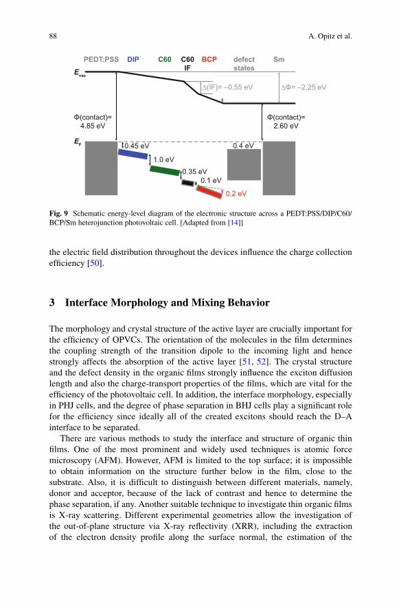
As an example, the full electronic structure of an OPVC made of a C60/DIP het-erojunction sandwiched between PEDT:PSS and samarium electrodes and includingan exciton blocking layer of bathocuproine (BCP) is displayed in Fig. 9 [14].Blocking layers made of BCP or bathophenanthroline (BPhen) were reported toreduce exciton quenching at the metal top contact and they simultaneously serve toprotect the C60 layer from metal penetration and damage during evaporation of thetop contact [46, 48, 49]. Energy-level shifts at the C60/BCP interface and inside theBCP layer are caused by a preferential orientation of BCP dipoles. The electrostaticfield drop across DIP/C60 is therefore reduced compared to the full effective work-function difference of the contact materials. Even if the photovoltaic gap at theactive interface is unaffected by the electrostatic potential landscape, changes in
88 A. Opitz et al.
Fig. 9 Schematic energy-level diagram of the electronic structure across a PEDT:PSS/DIP/C60/BCP/Sm heterojunction photovoltaic cell. [Adapted from [14]]
the electric field distribution throughout the devices influence the charge collectionefficiency [50].
3 Interface Morphology and Mixing Behavior
The morphology and crystal structure of the active layer are crucially important forthe efficiency of OPVCs. The orientation of the molecules in the film determinesthe coupling strength of the transition dipole to the incoming light and hencestrongly affects the absorption of the active layer [51, 52]. The crystal structureand the defect density in the organic films strongly influence the exciton diffusionlength and also the charge-transport properties of the films, which are vital for theefficiency of the photovoltaic cell. In addition, the interface morphology, especiallyin PHJ cells, and the degree of phase separation in BHJ cells play a significant rolefor the efficiency since ideally all of the created excitons should reach the D–Ainterface to be separated.
There are various methods to study the interface and structure of organic thinfilms. One of the most prominent and widely used techniques is atomic forcemicroscopy (AFM). However, AFM is limited to the top surface; it is impossibleto obtain information on the structure further below in the film, close to thesubstrate. Also, it is difficult to distinguish between different materials, namely,donor and acceptor, because of the lack of contrast and hence to determine thephase separation, if any. Another suitable technique to investigate thin organic filmsis X-ray scattering. Different experimental geometries allow the investigation ofthe out-of-plane structure via X-ray reflectivity (XRR), including the extractionof the electron density profile along the surface normal, the estimation of the
Charge Separation at Nanostructured Molecular D–A Interfaces 89
surface roughness, and the out-of-plane crystallinity of the film. Grazing-incidenceX-ray diffraction (GIXD) can be used to reveal the in-plane crystal structure ofthe film, and grazing-incidence small-angle X-ray scattering allows us to determinemorphological features like the surface island distance and their shape [53, 54]. Oneof the benefits of X-ray scattering is that it is possible to use it directly in situ duringthe preparation of the films and follow the film growth in a noninvasive way in realtime, giving a more detailed understanding of the film growth.
In general, there are several interfaces in OPVCs, all of which are important forthe efficiency. We focus on the D–A, so the organic–organic interface. For detailsof the interfaces between the active layer and the (metal) electrodes, which is initself a very complex and interesting topic, we refer to the literature [55, 56]. Inthe following we first focus on different interfaces occurring in PHJ geometries andafterward turn to effects observed in mixtures used in BHJ cells.
3.1 Interface in PHJ Geometries
As shown in Fig. 5a–c, the interface in PHJ can have different geometries. Obvi-ously, the schematics represent only ideal cases. In real thin films, the interfaces areusually not as well defined, and even the distinction between PHJ and BHJ is oftennot as clear as that depicted in Fig. 5.
The growth of an organic material on top of another one can differ from theobserved growth of this material on a bare substrate [57]. The growth of theoverlayer can strongly depend on the film properties of the materials underneath.The interactions between different organic materials might drastically differ fromthose between a bare substrate and an organic compound and can have a stronginfluence on the growth [31]. These interactions depend inter alia on the type ofenergetic arrangement, that is, whether dipole interactions or higher-order electronicinteractions dominate the van der Waals interaction, on the sterical compatibilityof the materials, which can lead to strain in the growth of the overlayer, and onthe orientation of the bottom material, for instance, a lying-down or standing-uporientation of rod-like molecules.
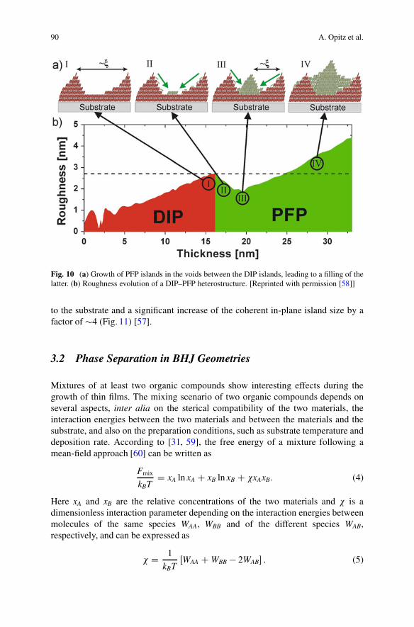
As an example, we show how real-time XRR can be used to characterize thegrowth of an organic heterostructure consisting of a PFP overlayer on top of DIP[58]. From the real-time data the roughness evolution of the film was extracted(Fig. 10). The PFP first fills the voids between the DIP islands, leading to asmoothing of the DIP layer. The resulting structure is very similar to the interfacesketched in Fig. 5b.
The growth of an organic compound on top of another can be different fromthe growth on a bare substrate. The structural order of C60 thin films is shown tobe significantly improved by inserting a templating layer of DIP between the SiO2substrate and C60. In contrast to growth on an amorphous substrate like SiO2, C60grown on DIP exhibits alignment of the fcc-domains with the (1 1 1) plane parallel
90 A. Opitz et al.
Fig. 10 (a) Growth of PFP islands in the voids between the DIP islands, leading to a filling of thelatter. (b) Roughness evolution of a DIP–PFP heterostructure. [Reprinted with permission [58]]
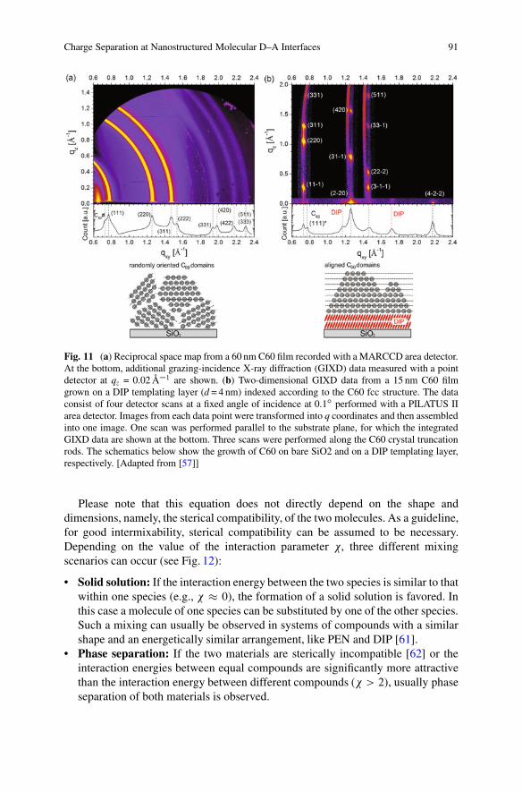
to the substrate and a significant increase of the coherent in-plane island size by afactor of �4 (Fig. 11) [57].
3.2 Phase Separation in BHJ Geometries
Mixtures of at least two organic compounds show interesting effects during thegrowth of thin films. The mixing scenario of two organic compounds depends onseveral aspects, inter alia on the sterical compatibility of the two materials, theinteraction energies between the two materials and between the materials and thesubstrate, and also on the preparation conditions, such as substrate temperature anddeposition rate. According to [31, 59], the free energy of a mixture following amean-field approach [60] can be written as
Fmix
kBTD xA ln xA C xB ln xB C �xAxB: (4)
Here xA and xB are the relative concentrations of the two materials and � is adimensionless interaction parameter depending on the interaction energies betweenmolecules of the same species WAA, WBB and of the different species WAB,respectively, and can be expressed as
� D 1
kBTŒWAA C WBB � 2WAB� : (5)
Charge Separation at Nanostructured Molecular D–A Interfaces 91
Fig. 11 (a) Reciprocal space map from a 60 nm C60 film recorded with a MARCCD area detector.At the bottom, additional grazing-incidence X-ray diffraction (GIXD) data measured with a pointdetector at qz = 0.02 Å�1 are shown. (b) Two-dimensional GIXD data from a 15 nm C60 filmgrown on a DIP templating layer (d = 4 nm) indexed according to the C60 fcc structure. The dataconsist of four detector scans at a fixed angle of incidence at 0.1ı performed with a PILATUS IIarea detector. Images from each data point were transformed into q coordinates and then assembledinto one image. One scan was performed parallel to the substrate plane, for which the integratedGIXD data are shown at the bottom. Three scans were performed along the C60 crystal truncationrods. The schematics below show the growth of C60 on bare SiO2 and on a DIP templating layer,respectively. [Adapted from [57]]
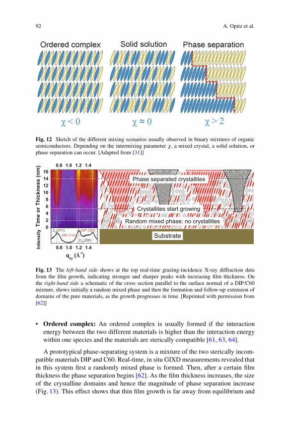
Please note that this equation does not directly depend on the shape anddimensions, namely, the sterical compatibility, of the two molecules. As a guideline,for good intermixability, sterical compatibility can be assumed to be necessary.Depending on the value of the interaction parameter �, three different mixingscenarios can occur (see Fig. 12):
• Solid solution: If the interaction energy between the two species is similar to thatwithin one species (e.g., � � 0), the formation of a solid solution is favored. Inthis case a molecule of one species can be substituted by one of the other species.Such a mixing can usually be observed in systems of compounds with a similarshape and an energetically similar arrangement, like PEN and DIP [61].
• Phase separation: If the two materials are sterically incompatible [62] or theinteraction energies between equal compounds are significantly more attractivethan the interaction energy between different compounds (� > 2), usually phaseseparation of both materials is observed.
92 A. Opitz et al.
Fig. 12 Sketch of the different mixing scenarios usually observed in binary mixtures of organicsemiconductors. Depending on the intermixing parameter �, a mixed crystal, a solid solution, orphase separation can occur. [Adapted from [31]]
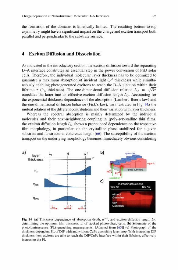
Fig. 13 The left-hand side shows at the top real-time grazing-incidence X-ray diffraction datafrom the film growth, indicating stronger and sharper peaks with increasing film thickness. Onthe right-hand side a schematic of the cross section parallel to the surface normal of a DIP:C60mixture, shows initially a random mixed phase and then the formation and follow-up extension ofdomains of the pure materials, as the growth progresses in time. [Reprinted with permission from[62]]
• Ordered complex: An ordered complex is usually formed if the interactionenergy between the two different materials is higher than the interaction energywithin one species and the materials are sterically compatible [61, 63, 64].
A prototypical phase-separating system is a mixture of the two sterically incom-patible materials DIP and C60. Real-time, in situ GIXD measurements revealed thatin this system first a randomly mixed phase is formed. Then, after a certain filmthickness the phase separation begins [62]. As the film thickness increases, the sizeof the crystalline domains and hence the magnitude of phase separation increase(Fig. 13). This effect shows that thin film growth is far away from equilibrium and
Charge Separation at Nanostructured Molecular D–A Interfaces 93
the formation of the domains is kinetically limited. The resulting bottom-to-topasymmetry might have a significant impact on the charge and exciton transport bothparallel and perpendicular to the substrate surface.
4 Exciton Diffusion and Dissociation
As indicated in the introductory section, the exciton diffusion toward the separatingD–A interface constitutes an essential step in the power conversion of PHJ solarcells. Therefore, the individual molecular layer thickness has to be optimized toguarantee a maximum absorption of incident light (% thickness) while simulta-neously enabling photogenerated excitons to reach the D–A junction within theirlifetime � (& thickness). The one-dimensional diffusion relation LD D p
D�
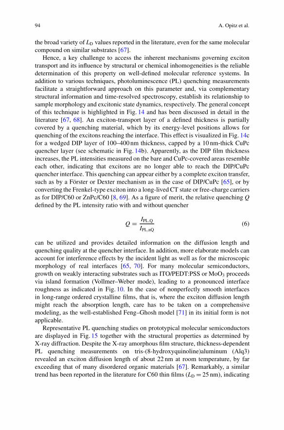
translates the latter into an effective exciton diffusion length LD. Accounting forthe exponential thickness dependence of the absorption (Lambert–Beer’s law) andthe one-dimensional diffusion behavior (Fick’s law), we illustrated in Fig. 14a themutual relation of the different contributions and their variation with layer thickness.
Whereas the spectral absorption is mainly determined by the individualmolecules and their next-neighboring coupling in (poly-)crystalline thin films,the exciton diffusion length LD shows a pronounced dependence on the respectivefilm morphology, in particular, on the crystalline phase stabilized for a givensubstrate and its structural coherence length [66]. The susceptibility of the excitontransport on the underlying morphology becomes immediately obvious considering
Fig. 14 (a) Thickness dependence of absorption depth, ˛�1, and exciton diffusion length LD,determining the optimum film thickness, d, of stacked photovoltaic cells. (b) Schematic of thephotoluminescence (PL) quenching measurements. [Adapted from [65]] (c) Photograph of thethickness-dependent PL of DIP with and without CuPc quenching layer atop. With increasing DIPthickness, less excitons are able to reach the DIP/CuPc interface within their lifetime, effectivelyincreasing the PL
94 A. Opitz et al.
the broad variety of LD values reported in the literature, even for the same molecularcompound on similar substrates [67].
Hence, a key challenge to access the inherent mechanisms governing excitontransport and its influence by structural or chemical inhomogeneities is the reliabledetermination of this property on well-defined molecular reference systems. Inaddition to various techniques, photoluminescence (PL) quenching measurementsfacilitate a straightforward approach on this parameter and, via complementarystructural information and time-resolved spectroscopy, establish its relationship tosample morphology and excitonic state dynamics, respectively. The general conceptof this technique is highlighted in Fig. 14 and has been discussed in detail in theliterature [67, 68]. An exciton-transport layer of a defined thickness is partiallycovered by a quenching material, which by its energy-level positions allows forquenching of the excitons reaching the interface. This effect is visualized in Fig. 14cfor a wedged DIP layer of 100–400 nm thickness, capped by a 10 nm-thick CuPcquencher layer (see schematic in Fig. 14b). Apparently, as the DIP film thicknessincreases, the PL intensities measured on the bare and CuPc-covered areas resembleeach other, indicating that excitons are no longer able to reach the DIP/CuPcquencher interface. This quenching can appear either by a complete exciton transfer,such as by a Förster or Dexter mechanism as in the case of DIP/CuPc [65], or byconverting the Frenkel-type exciton into a long-lived CT state or free-charge carriersas for DIP/C60 or ZnPc/C60 [8, 69]. As a figure of merit, the relative quenching Qdefined by the PL intensity ratio with and without quencher
Q D IPL;Q
IPL;nQ(6)
can be utilized and provides detailed information on the diffusion length andquenching quality at the quencher interface. In addition, more elaborate models canaccount for interference effects by the incident light as well as for the microscopicmorphology of real interfaces [65, 70]. For many molecular semiconductors,growth on weakly interacting substrates such as ITO/PEDT:PSS or MoO3 proceedsvia island formation (Vollmer–Weber mode), leading to a pronounced interfaceroughness as indicated in Fig. 10. In the case of nonperfectly smooth interfacesin long-range ordered crystalline films, that is, where the exciton diffusion lengthmight reach the absorption length, care has to be taken on a comprehensivemodeling, as the well-established Feng–Ghosh model [71] in its initial form is notapplicable.
Representative PL quenching studies on prototypical molecular semiconductorsare displayed in Fig. 15 together with the structural properties as determined byX-ray diffraction. Despite the X-ray amorphous film structure, thickness-dependentPL quenching measurements on tris-(8-hydroxyquinoline)aluminum (Alq3)revealed an exciton diffusion length of about 22 nm at room temperature, by farexceeding that of many disordered organic materials [67]. Remarkably, a similartrend has been reported in the literature for C60 thin films (LD D 25 nm), indicating
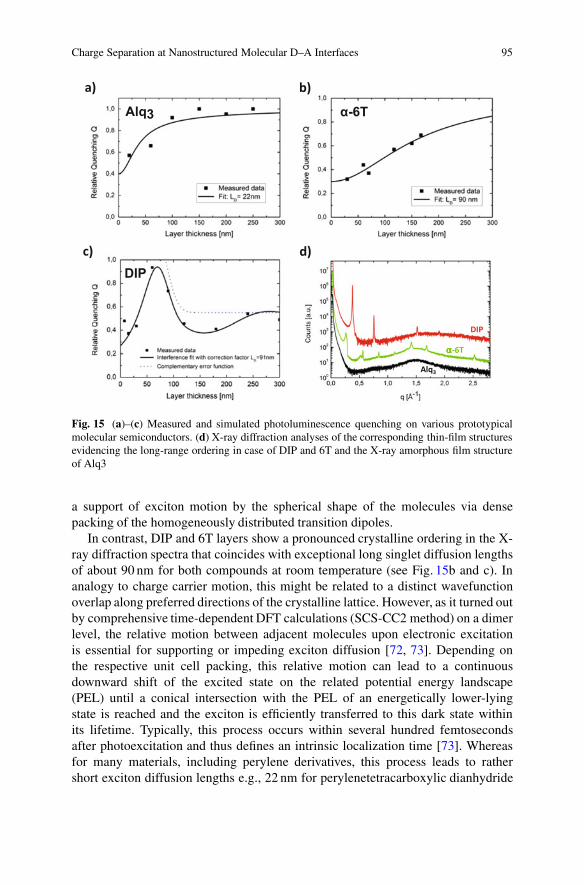
Charge Separation at Nanostructured Molecular D–A Interfaces 95
Fig. 15 (a)–(c) Measured and simulated photoluminescence quenching on various prototypicalmolecular semiconductors. (d) X-ray diffraction analyses of the corresponding thin-film structuresevidencing the long-range ordering in case of DIP and 6T and the X-ray amorphous film structureof Alq3
a support of exciton motion by the spherical shape of the molecules via densepacking of the homogeneously distributed transition dipoles.
In contrast, DIP and 6T layers show a pronounced crystalline ordering in the X-ray diffraction spectra that coincides with exceptional long singlet diffusion lengthsof about 90 nm for both compounds at room temperature (see Fig. 15b and c). Inanalogy to charge carrier motion, this might be related to a distinct wavefunctionoverlap along preferred directions of the crystalline lattice. However, as it turned outby comprehensive time-dependent DFT calculations (SCS-CC2 method) on a dimerlevel, the relative motion between adjacent molecules upon electronic excitationis essential for supporting or impeding exciton diffusion [72, 73]. Depending onthe respective unit cell packing, this relative motion can lead to a continuousdownward shift of the excited state on the related potential energy landscape(PEL) until a conical intersection with the PEL of an energetically lower-lyingstate is reached and the exciton is efficiently transferred to this dark state withinits lifetime. Typically, this process occurs within several hundred femtosecondsafter photoexcitation and thus defines an intrinsic localization time [73]. Whereasfor many materials, including perylene derivatives, this process leads to rathershort exciton diffusion lengths e.g., 22 nm for perylenetetracarboxylic dianhydride
96 A. Opitz et al.
(˛-PTCDA), in agreement with the literature [66], the situation differs remarkablywith DIP. Because of the specific alignment of molecular pairs within the thin-filmunit cell, the intermolecular motion upon electronic excitation imposes an energybarrier on the related energy manifold, which prevents excitons from reachingthe conical intersection and thereby extends their effective diffusion length. Asa consequence of this steric hindrance, LD is mainly governed by the radiativelifetime of the excited state and the spatial extension of crystalline grains. This wasevidenced by temperature-dependent PL quenching studies on DIP as well as 6Trendering exciton transport to be nonthermally activated below a critical temperatureand film thickness. This observation was explained by a reduced exciton–phononscattering at low temperatures and hints at a coherent exciton motion within thecrystalline grains [65]. Furthermore, in such long-range ordered crystalline systemsefficient exciton trapping might occur at grain boundaries, where the structuralconstraints are lifted, as reported for rubrene microcrystals [74].
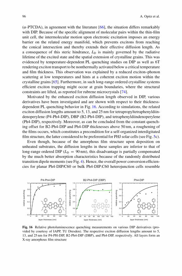
Motivated by the enhanced exciton diffusion length observed in DIP, variousderivatives have been investigated and are shown with respect to their thickness-dependent PL quenching behavior in Fig. 16. According to simulations, the relatedexciton diffusion lengths amount to 5, 13, and 25 nm for tetrapropyltetraphenyldiin-denoperylene (P4-Ph4-DIP), DBP (B2-Ph4-DIP), and tetraphenyldiindenoperylene(Ph4-DIP), respectively. Moreover, as can be concluded from the constant quench-ing offset for B2-Ph4-DIP and Ph4-DIP thicknesses above 50 nm, a roughening ofthe films occurs, which constitutes a precondition for a self-organized interdigitatedfilm structure, the latter considered to be preferential for PHJ solar cells (see Fig. 5c).
Even though, because of the amorphous film structure upon deposition onunheated substrates, the diffusion lengths in these samples are inferior to that oflong-range ordered DIP (LD D 90 nm), this disadvantage is partially compensatedby the much better absorption characteristics because of the randomly distributedtransition dipole moments (see Fig. 4). Hence, the overall power conversion efficien-cies for planar Ph4-DIP/C60 or bulk Ph4-DIP:C60 heterojunction cells resemble
0
rela
tive
quen
chin
g
rela
tive
quen
chin
g
rela
tive
quen
chin
g
0.0
0.2
0.4
0.6
0.8
1.0
0.0
0.2
0.4
0.6
0.8
1.0
0.0
0.2
0.4
0.6
0.8
1.0
20 40
layer thickness (nm)
P4-Ph4-DIP B2-Ph4-DIP (DBP) Ph4-DIP
layer thickness (nm) layer thickness (nm)
60 80 100 120 0 20 40 60 80 100 1200 20 40 60 80 100 120 140 160
Fig. 16 Relative photoluminescence quenching measurements on various DIP derivatives (pro-vided by courtesy of IAPP, TU Dresden). The respective exciton diffusion lengths amount to 5,13, and 25 nm for P4-PH-DIP, B2-Ph4-DIP (DBP), and Ph4-DIP, respectively. All layers form anX-ray amorphous film structure
Charge Separation at Nanostructured Molecular D–A Interfaces 97
those of the corresponding DIP devices, but with the additional possibility of furtherenhancing the crystalline order by, for instance, thermal treatment [75].
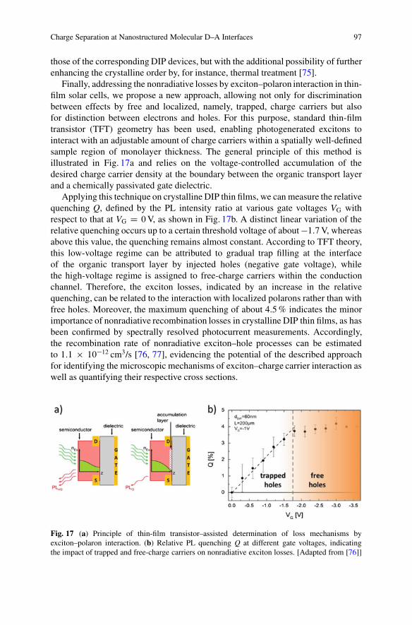
Finally, addressing the nonradiative losses by exciton–polaron interaction in thin-film solar cells, we propose a new approach, allowing not only for discriminationbetween effects by free and localized, namely, trapped, charge carriers but alsofor distinction between electrons and holes. For this purpose, standard thin-filmtransistor (TFT) geometry has been used, enabling photogenerated excitons tointeract with an adjustable amount of charge carriers within a spatially well-definedsample region of monolayer thickness. The general principle of this method isillustrated in Fig. 17a and relies on the voltage-controlled accumulation of thedesired charge carrier density at the boundary between the organic transport layerand a chemically passivated gate dielectric.
Applying this technique on crystalline DIP thin films, we can measure the relativequenching Q, defined by the PL intensity ratio at various gate voltages VG withrespect to that at VG D 0 V, as shown in Fig. 17b. A distinct linear variation of therelative quenching occurs up to a certain threshold voltage of about �1:7 V, whereasabove this value, the quenching remains almost constant. According to TFT theory,this low-voltage regime can be attributed to gradual trap filling at the interfaceof the organic transport layer by injected holes (negative gate voltage), whilethe high-voltage regime is assigned to free-charge carriers within the conductionchannel. Therefore, the exciton losses, indicated by an increase in the relativequenching, can be related to the interaction with localized polarons rather than withfree holes. Moreover, the maximum quenching of about 4.5 % indicates the minorimportance of nonradiative recombination losses in crystalline DIP thin films, as hasbeen confirmed by spectrally resolved photocurrent measurements. Accordingly,the recombination rate of nonradiative exciton–hole processes can be estimatedto 1:1 � 10�12 cm3/s [76, 77], evidencing the potential of the described approachfor identifying the microscopic mechanisms of exciton–charge carrier interaction aswell as quantifying their respective cross sections.
Fig. 17 (a) Principle of thin-film transistor–assisted determination of loss mechanisms byexciton–polaron interaction. (b) Relative PL quenching Q at different gate voltages, indicatingthe impact of trapped and free-charge carriers on nonradiative exciton losses. [Adapted from [76]]
98 A. Opitz et al.
Based on the experimental findings and theoretical results, one can develop gen-eral strategies toward a rational design of molecular compounds, further improvingexisting device concepts by an optimized PHJ architecture with respect to excitongeneration and transport.
5 Charge Transport and Device Performance
Solar cells have been investigated for various D–A combinations shown in Figs. 2–4(see [12, 25, 36, 78–80]). Among them DIP/C60 turned out to be a model system,because in-depth studies of the electronic structure, morphology, and excitontransport were available. Remarkably, DIP grows in a crystalline fashion onmany technical substrates and, in particular, on ITO covered with PEDT:PSS orHIL1.3 used as anode for OPVCs in this study. Even without substrate heating,the molecules form crystalline domains with sizes of a few tens of nanometersand for heated substrates (with TS � 100 ıC) the lateral domain size reachesalmost micron dimensions. This high degree of structural order is reflected in goodcharge-transport properties of DIP, reaching carrier mobilities of 10�1 cm2/Vs forholes as well as electrons in field-effect transistors [81]. This ambipolar transportbehavior, together with its energy levels being intermediate between many classicaldonor and acceptor materials (see Fig. 3), make DIP a unique candidate forimplementation as both donor or acceptor, depending on the partner material [78].On the one hand, it is a donor with respect to fullerenes, but with significantlylarger VOC than CuPc, 6T, or PEN. On the other hand, it can also be used as anacceptor for 6T and its polymeric analogue P3HT, yielding a VOC of more than1.3 V.
Figure 18 shows the photoelectrical characteristics of DIP and its relatedanalogue DBP combined with C60 or C70 in different architectures. DIP/C60cells yield a high open-circuit voltage exceeding 0.9 V and high fill factors (up to75 %); however, they lack in current because as a result of the upright-standingDIP growth, there is basically no photon absorption and therefore no significantcontribution of DIP to the photocurrent (see Fig. 18c). This deficit can be improvedby using DBP with a lying orientation as the donor material. As the EQE spectraclearly show, there is now an equivalent contribution of both materials. Furtherimprovement of JSC is possible if the fullerene C70 is used as acceptor, whichhas a higher absorption than C60 because of the lower symmetry of the molecule.Nevertheless, as the photocurrent spectra show, part of the improvement comes atthe expense of less photocurrent from DBP. The latter can be enhanced if a thinlayer of ˛-NPD is introduced as an exciton-blocking layer to prevent quenching atthe interface to the highly conducting PEDT:PSS. The biggest increase in short-circuit current, however, is achieved when the PHJ architecture is replaced by aPM-HJ—in this case DBP mixed with C70 in a 1:2 ratio by weight. As Fig. 18shows, the current almost doubles and an EQE between 70–80 % is achieved overa wide range. From the point of view of exciton quenching, the ˛-NPD layer
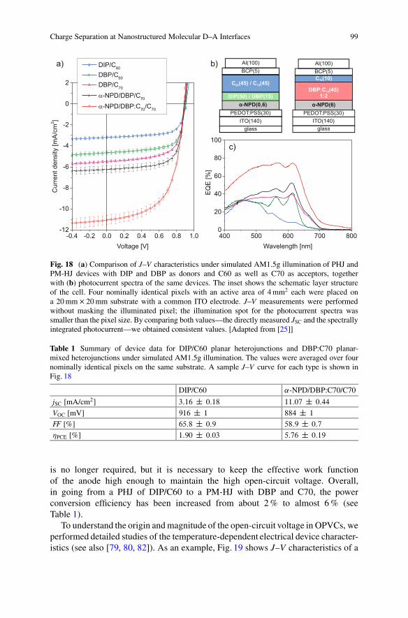
Charge Separation at Nanostructured Molecular D–A Interfaces 99
Fig. 18 (a) Comparison of J–V characteristics under simulated AM1.5g illumination of PHJ andPM-HJ devices with DIP and DBP as donors and C60 as well as C70 as acceptors, togetherwith (b) photocurrent spectra of the same devices. The inset shows the schematic layer structureof the cell. Four nominally identical pixels with an active area of 4 mm2 each were placed ona 20 mm � 20 mm substrate with a common ITO electrode. J–V measurements were performedwithout masking the illuminated pixel; the illumination spot for the photocurrent spectra wassmaller than the pixel size. By comparing both values—the directly measured JSC and the spectrallyintegrated photocurrent—we obtained consistent values. [Adapted from [25]]
Table 1 Summary of device data for DIP/C60 planar heterojunctions and DBP:C70 planar-mixed heterojunctions under simulated AM1.5g illumination. The values were averaged over fournominally identical pixels on the same substrate. A sample J–V curve for each type is shown inFig. 18
DIP/C60 ˛-NPD/DBP:C70/C70
jSC [mA/cm2] 3:16 ˙ 0:18 11:07 ˙ 0:44
VOC [mV] 916 ˙ 1 884 ˙ 1
FF [%] 65:8 ˙ 0:9 58:9 ˙ 0:7
�PCE [%] 1:90 ˙ 0:03 5:76 ˙ 0:19
is no longer required, but it is necessary to keep the effective work functionof the anode high enough to maintain the high open-circuit voltage. Overall,in going from a PHJ of DIP/C60 to a PM-HJ with DBP and C70, the powerconversion efficiency has been increased from about 2 % to almost 6 % (seeTable 1).
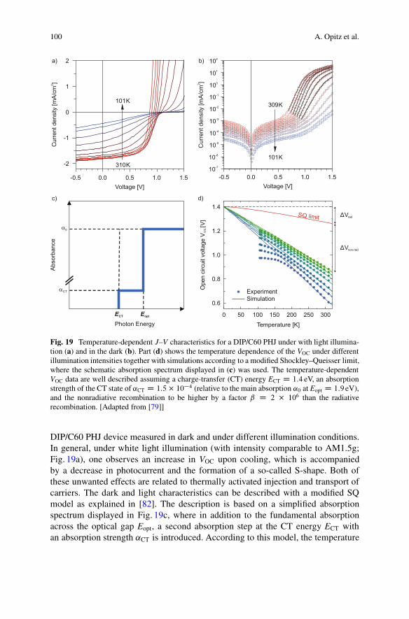
To understand the origin and magnitude of the open-circuit voltage in OPVCs, weperformed detailed studies of the temperature-dependent electrical device character-istics (see also [79, 80, 82]). As an example, Fig. 19 shows J–V characteristics of a
100 A. Opitz et al.
Fig. 19 Temperature-dependent J–V characteristics for a DIP/C60 PHJ under with light illumina-tion (a) and in the dark (b). Part (d) shows the temperature dependence of the VOC under differentillumination intensities together with simulations according to a modified Shockley–Queisser limit,where the schematic absorption spectrum displayed in (c) was used. The temperature-dependentVOC data are well described assuming a charge-transfer (CT) energy ECT D 1:4 eV, an absorptionstrength of the CT state of ˛CT D 1:5 � 10�4 (relative to the main absorption ˛0 at Eopt D 1:9 eV),and the nonradiative recombination to be higher by a factor ˇ D 2 � 106 than the radiativerecombination. [Adapted from [79]]
DIP/C60 PHJ device measured in dark and under different illumination conditions.In general, under white light illumination (with intensity comparable to AM1.5g;Fig. 19a), one observes an increase in VOC upon cooling, which is accompaniedby a decrease in photocurrent and the formation of a so-called S-shape. Both ofthese unwanted effects are related to thermally activated injection and transport ofcarriers. The dark and light characteristics can be described with a modified SQmodel as explained in [82]. The description is based on a simplified absorptionspectrum displayed in Fig. 19c, where in addition to the fundamental absorptionacross the optical gap Eopt, a second absorption step at the CT energy ECT withan absorption strength ˛CT is introduced. According to this model, the temperature
Charge Separation at Nanostructured Molecular D–A Interfaces 101
dependence of VOC follows a relation [7, 83]:
VOC D ECT
e� �Vrad � �Vnon-rad ; (7)
where both, the radiative and nonradiative loss terms depend approximately linearlyon the temperature [79]. Thus, from the temperature and intensity-dependentVOC data shown in Fig. 19d, one obtains a CT energy of 1.4 eV, which setsthe upper limit for the chemical potential of photogenerated charge carriers atT D 0 K. Additionally, the graph shows that the major loss at room temperatureis caused by nonradiative recombination (�Vnon-rad � 0:4 V)—in agreement withthe nonradiative recombination current being more than six orders of magnitudehigher than the radiative one, whereas the thermodynamically unavoidable radiativerecombination across the CT gap amounts to a loss �Vrad of only 0.1 V. Thisexemplifies that the energy loss between the CT state and the open-circuit voltageis of the order of 0.5 eV and thus in the same range as in many polymer/fullereneOPVCs [7]. However, one has to keep in mind that an additional energy loss occursby the formation of the CT state in the course of exciton dissociation at the D–Ainterface (see Fig. 1).
The apparently linear extrapolation of the measured VOC.T/ toward T D 0 Kalso deserves some comment. Since the introduction by Vandewal et al. [7], thisapproach to determining the relevant photovoltaic gap has been frequently used inthe literature [82, 84]. However, as we have found with the system 6T/DIP, it canoverestimate the actual CT energy at the D–A interface if the CT gap is close tothe optical gap of one of the two materials and if the electronic coupling betweenboth of them is extremely weak, as is the case for the standing orientation of bothmolecules on top of each other [80]. In this case, a linear extrapolation of measuredVOC.T/ data yields the optical gap of DIP, which indicates that this is the dominantrecombination pathway at higher temperatures.
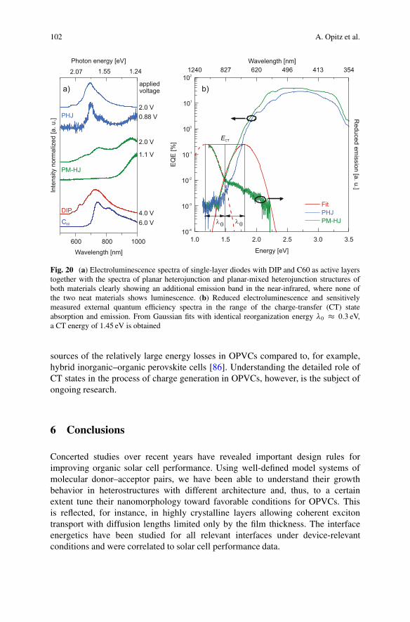
Direct spectroscopic access to CT states in OPVCs can be obtained fromelectroluminescence (EL) and photocurrent spectra measured with high sensitivitybelow the optical gap of the main absorber [85]. Figure 20a shows EL spectra ofdiodes with neat layers of DIP and C60 each, which are compared to EL spectra ofPHJ and PM-HJ of both materials, where the OPVCs are operated as light-emittingdevices in the forward bias regime. For both D–A heterojunctions one observes abroad emission band in the near-infrared region (850–1000 nm), where none of theneat materials shows luminescence. In particular for the PM-HJ, the EL measuredclose to VOC stems exclusively from light emission from CT states. A quantitativeanalysis combining the reduced emission spectrum with the EQE spectrum asshown in Fig. 20b reveals a CT energy of 1.45 eV, in excellent agreement with thetemperature-dependent electrical measurements discussed above. What the spectraalso show is a fairly large Stokes shift between CT absorption (modeled as aGaussian in the low-energy onset of the EQE spectrum) and CT emission, reflectedin a shift between both maxima of twice the reorganization energy �0 � 0:3 eV.This large shift together with the low EL quantum efficiency can be seen as major
102 A. Opitz et al.
Fig. 20 (a) Electroluminescence spectra of single-layer diodes with DIP and C60 as active layerstogether with the spectra of planar heterojunction and planar-mixed heterojunction structures ofboth materials clearly showing an additional emission band in the near-infrared, where none ofthe two neat materials shows luminescence. (b) Reduced electroluminescence and sensitivelymeasured external quantum efficiency spectra in the range of the charge-transfer (CT) stateabsorption and emission. From Gaussian fits with identical reorganization energy �0 � 0:3 eV,a CT energy of 1.45 eV is obtained
sources of the relatively large energy losses in OPVCs compared to, for example,hybrid inorganic–organic perovskite cells [86]. Understanding the detailed role ofCT states in the process of charge generation in OPVCs, however, is the subject ofongoing research.
6 Conclusions
Concerted studies over recent years have revealed important design rules forimproving organic solar cell performance. Using well-defined model systems ofmolecular donor–acceptor pairs, we have been able to understand their growthbehavior in heterostructures with different architecture and, thus, to a certainextent tune their nanomorphology toward favorable conditions for OPVCs. Thisis reflected, for instance, in highly crystalline layers allowing coherent excitontransport with diffusion lengths limited only by the film thickness. The interfaceenergetics have been studied for all relevant interfaces under device-relevantconditions and were correlated to solar cell performance data.
Charge Separation at Nanostructured Molecular D–A Interfaces 103
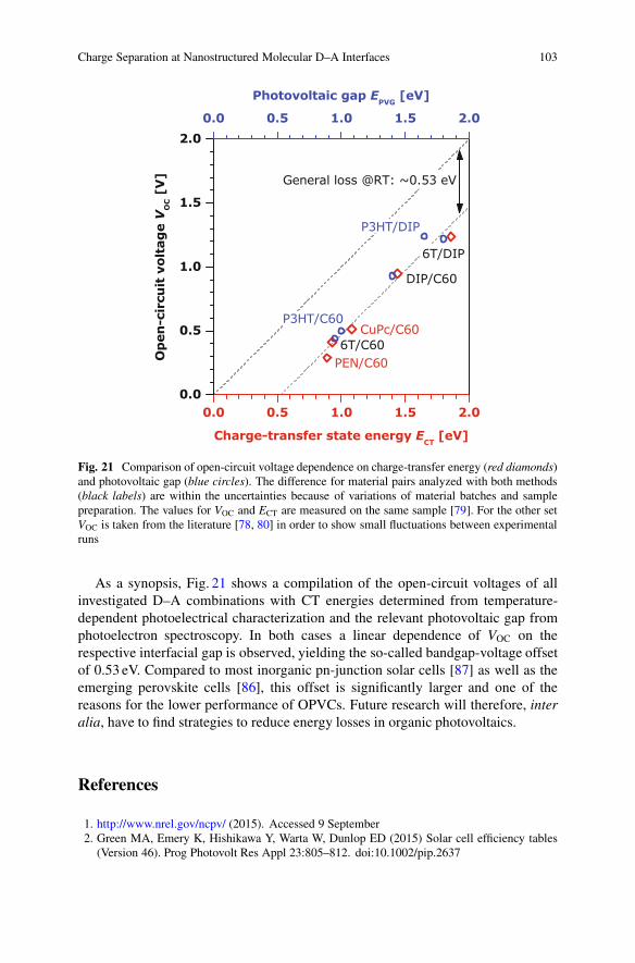
Fig. 21 Comparison of open-circuit voltage dependence on charge-transfer energy (red diamonds)and photovoltaic gap (blue circles). The difference for material pairs analyzed with both methods(black labels) are within the uncertainties because of variations of material batches and samplepreparation. The values for VOC and ECT are measured on the same sample [79]. For the other setVOC is taken from the literature [78, 80] in order to show small fluctuations between experimentalruns
As a synopsis, Fig. 21 shows a compilation of the open-circuit voltages of allinvestigated D–A combinations with CT energies determined from temperature-dependent photoelectrical characterization and the relevant photovoltaic gap fromphotoelectron spectroscopy. In both cases a linear dependence of VOC on therespective interfacial gap is observed, yielding the so-called bandgap-voltage offsetof 0.53 eV. Compared to most inorganic pn-junction solar cells [87] as well as theemerging perovskite cells [86], this offset is significantly larger and one of thereasons for the lower performance of OPVCs. Future research will therefore, interalia, have to find strategies to reduce energy losses in organic photovoltaics.
References
1. http://www.nrel.gov/ncpv/ (2015). Accessed 9 September2. Green MA, Emery K, Hishikawa Y, Warta W, Dunlop ED (2015) Solar cell efficiency tables
(Version 46). Prog Photovolt Res Appl 23:805–812. doi:10.1002/pip.2637
104 A. Opitz et al.
3. Shockley W, Queisser HJ (1961) Detailed balance limit of efficiency of p-n junction solar cells.J Appl Phys 32:510–519. doi:10.1063/1.1736034
4. Veldman D, Meskers SCJ, Janssen RAJ (2009) The energy of charge-transfer states in electrondonor-acceptor blends: insight into the energy losses in organic solar cells. Adv Funct Mater19:1939–1948. doi:10.1002/adfm.200900090
5. Clarke TM, Durrant JR (2010) Charge photogeneration in organic solar cells. Chem Rev110:6736–6767. doi:10.1021/cr900271s
6. Deibel C, Dyakonov V (2010) Polymerfullerene bulk heterojunction solar cells. Rep Prog Phys73:096401. doi:10.1088/0034-4885/73/9/096401
7. Vandewal K, Tvingstedt K, Gadisa A, Inganäs O, Manca JV (2010) Relating the open-circuitvoltage to interface molecular properties of donor:acceptor bulk heterojunction solar cells. PhysRev B 81:125204. doi:10.1103/PhysRevB.81.125204
8. Opitz A, Wagner J, Brütting W, Salzmann I, Koch N, Manara J, Pflaum J, Hinderhofer A,Schreiber F (2010) Charge separation at molecular donor–acceptor interfaces: correlationbetween morphology and solar cell performance. IEEE J Sel Top Quant 16:1707–1717.doi:10.1109/JSTQE.2010.2048096
9. Forrest SR (2011) The limits to organic photovoltaic cell efficiency. MRS Bull 30:28–32.doi:10.1557/mrs2005.5
10. Wilke A, Mizokuro T, Blum RP, Rabe JP, Koch N (2010) IEEE J Sel Top Quant 16:1732–1737.doi:10.1109/JSTQE.2010.2042035
11. Salzmann I, Duhm S, Heimel G, Oehzelt M, Kniprath R, Johnson RL, Rabe JP, Koch N (2008)Tuning the ionization energy of organic semiconductor films: the role of intramolecular polarbonds. J Am Chem Soc 130:12870–12871. doi:10.1021/ja804793a
12. Wagner J, Gruber M, Hinderhofer A, Wilke A, Bröker B, Frisch J, Amsalem P, Vollmer A,Opitz A, Koch N, Schreiber F, Brütting W (2010) High fill factor and open circuit voltage inorganic photovoltaic cells with diindenoperylene as donor material. Adv Funct Mater 20:4295–4303. doi:10.1002/adfm.201001028
13. Pfützner S (2012) Studies on organic solar cells composed of fullerenes and zinc-phthalocyanines. Ph.D. thesis, TU Dresden. http://nbn-resolving.de/urn:nbn:de:bsz:14-qucosa-83486
14. Opitz A, Frisch J, Schlesinger R, Wilke A, Koch N (2013) Energy level alignment atinterfaces in organic photovoltaic devices. J Electron Spectrosc Relat Phenom 190:12–24.doi:10.1016/j.elspec.2012.11.008
15. Lau KM, Tang JX, Sun HY, Lee CS, Lee ST, Yan D (2006) Interfacial electronic structure ofcopper phthalocyanine and copper hexadecafluorophthalocyanine studied by photoemission.Appl Phys Lett 88:173513. doi:10.1063/1.2198484
16. Krause S, Casu MB, Schöll A, Umbach E (2008) Determination of transport levels of organicsemiconductors by UPS and IPS. New J Phys 10:085001. doi:10.1088/1367-2630/10/8/085001
17. Wilke A, Endres J, Hörmann U, Niederhausen J, Schlesinger R, Frisch J, Amsalem P, WagnerJ, Gruber M, Opitz A, Vollmer A, Brütting W, Kahn A, Koch N (2012) Correlation betweeninterface energetics and open circuit voltage in organic photovoltaic cells. Appl Phys Lett101:233301. doi:10.1063/1.4769360
18. Han W, Yoshida H, Ueno N, Kera S (2013) Electron affinity of pentacene thin film studiedby radiation-damage free inverse photoemission spectroscopy. Appl Phys Lett 103:123303.doi:10.1063/1.4821445
19. Brinkmann H, Kelting C, Makarov S, Tsaryova O, Schnurpfeil G, Wöhrle D, Schlettwein D(2008) Fluorinated phthalocyanines as molecular semiconductor thin films. Phys Stat Sol A205:409–420. doi:10.1002/pssa.200723391
20. Djurovich PI, Mayo EI, Forrest SR, Thompson ME (2009) Measurement of the lowestunoccupied molecular orbital energies of molecular organic semiconductors. Org Electron10:515–520. doi:10.1016/j.orgel.2008.12.011
21. Sze SM, Ng KK (2007) Physics of semiconductor devices, 3rd edn. Wiley, New York.doi:10.1002/0470068329
Charge Separation at Nanostructured Molecular D–A Interfaces 105
22. Rand B, Burk D, Forrest S (2007) Offset energies at organic semiconductor heterojunctionsand their influence on the open-circuit voltage of thin-film solar cells. Phys Rev B 75:115327.doi:10.1103/PhysRevB.75.115327
23. Riede M, Mueller T, Tress W, Schueppel R, Leo K (2008) Small-molecule solar cells-statusand perspectives. Nanotechnology 19:424001. doi:10.1088/0957-4484/19/42/424001
24. Stübinger T, Brütting W (2001) Exciton diffusion and optical interference in organic donor–acceptor photovoltaic cells. J Appl Phys 90:3632–3641. doi:10.1063/1.1394920
25. Grob S, Gruber M, Bartynski AN, Hörmann U, Linderl T, Thompson ME, Brütting W (2014)Amorphous vs crystalline exciton blocking layers at the anode interface in planar and planar-mixed heterojunction organic solar cells. Appl Phys Lett 104:213304. doi:10.1063/1.4879839
26. Tang CW (1986) Two-layer organic photovoltaic cell. Appl Phys Lett 48:183–185.doi:10.1063/1.96937
27. Yu S, Klimm C, Schäfer P, Rabe JP, Rech B, Koch N (2011) Organic photovoltaic cellswith interdigitated structures based on pentacene nanocolumn arrays. Org Electron 12:2180.doi:10.1016/j.orgel.2011.09.021
28. Yu S, Opitz A, Grob S, Resel R, Oehzelt M, Brütting W, Salzmann I, Koch N (2014) Per-formance enhancement of diindenoperylene-based organic photovoltaic cells by nanocolumn-arrays. Org. Electron. 15:2210–2217. doi:10.1016/j.orgel.2014.06.023
29. Salzmann I, Duhm S, Opitz R, Johnson RL, Rabe JP, Koch N (2008) Structural andelectronic properties of pentacene-fullerene heterojunctions. J Appl Phys 104:114518.doi:10.1063/1.3040003
30. Peumans P, Uchida S, Forrest SR (2003) Efficient bulk heterojunction photovoltaic cells usingsmall-molecular-weight organic thin films. Nature 425:158–162. doi:10.1038/nature01949
31. Hinderhofer A, Schreiber F (2012) Organic-organic heterostructures: concepts and applica-tions. ChemPhysChem 13:628–643. doi:10.1002/cphc.201100737
32. Opitz A, Ecker B, Wagner J, Hinderhofer A, Schreiber F, Manara J, Pflaum J, Brüt-ting W (2009) Mixed crystalline films of co-evaporated hydrogen- and fluorine-terminatedphthalocyanines and their application in photovoltaic devices. Org Electron 10:1259–1267.doi:10.1016/j.orgel.2009.07.004
33. Hinderhofer A, Frank C, Hosokai T, Resta A, Gerlach A, Schreiber F (2011) Structure and mor-phology of coevaporated pentacene-peruoropentacene thin films. J Chem Phys 134:104702.doi:10.1063/1.3557476
34. Reinhardt JP, Hinderhofer A, Broch K, Heinemeyer U, Kowarik S, Vorobiev A, GerlachA, Schreiber F (2012) Structural and Optical Properties of Mixed Diindenoperylene–Perfluoropentacene Thin Films. J Phys Chem C 116:10917–10923. doi:10.1021/jp211947y
35. Opitz A, Wagner J, Brütting W, Hinderhofer A, Schreiber F (2009) Molecular semiconductorblends: Microstructure, charge carrier transport, and application in photovoltaic cells. Phys StatSol A 206:2683–2694. doi:10.1002/pssa.200925238
36. Gruber M, Rawolle M, Wagner J, Magerl D, Hörmann U, Perlich J, Roth SV, Opitz A,Schreiber F, Müller-Buschbaum P, Brütting W (2013) Correlating structure and morphologyto device performance of molecular organic donor-acceptor photovoltaic cells based on diin-denoperylene (DIP) and C 60. Adv Energy Mater 3:1075–1083. doi:10.1002/aenm.201201012
37. Ishii H, Sugiyama K, Ito E, Seki K (1999) Energy level alignment and interfacial elec-tronic structures at organic/metal and organic/organic interfaces. Adv Mater 11:605–625.doi:10.1002/(SICI)1521-4095(199906)11:8<605::AID-ADMA605>3.0.CO;2-Q
38. Cahen D, Kahn A (2003) Electron energetics at surfaces and interfaces: concepts andexperiments. Adv Mater 15:271–277. doi:10.1002/adma.200390065
39. Koch N (2007) Organic electronic devices and their functional interfaces. ChemPhysChem8:1438–1455. doi:10.1002/cphc.200700177
40. Ueno N, Kera S (2008) Electron spectroscopy of functional organic thin films: deep insightsinto valence electronic structure in relation to charge transport property. Prog Surf Sci 83:490–557. doi:10.1016/j.progsurf.2008.10.002
106 A. Opitz et al.
41. Wu C, Hirose Y, Sirringhaus H, Kahn A (1997) Electron-hole interaction energy in theorganic molecular semiconductor PTCDA. Chem Phys Lett 272:43–47. doi:10.1016/S0009-2614(97)00481-8
42. Oehzelt M, Koch N, Heimel G (2014) Organic semiconductor density of states controls theenergy level alignment at electrode interfaces. Nat Commun 5:4174. doi:10.1038/ncomms5174
43. Wang H, Amsalem P, Heimel G, Salzmann I, Koch N, Oehzelt M (2014) Adv Mater 26:925–930. doi:10.1002/adma.201303467
44. Akaike K, Koch N, Oehzelt M (2014) Fermi level pinning induced electrostatic fields and bandbending at organic heterojunctions. Appl Phys Lett 105:223303. doi:10.1063/1.4903360
45. Wilke A, Amsalem P, Frisch J, Bröker B, Vollmer A, Koch N (2011) Electric fieldsinduced by energy level pinning at organic heterojunctions. Appl Phys Lett 98:123304.doi:10.1063/1.3571286
46. Wagner J, Gruber M, Wilke A, Tanaka Y, Topczak K, Steindamm A, Hörmann U, Opitz A,Nakayama Y, Ishii H, Pflaum J, Koch N, Brütting W (2012) Identification of different originsfor s-shaped current voltage characteristics in planar heterojunction organic solar cells. J ApplPhys 111:054509. doi:10.1063/1.3692050
47. Amsalem P, Niederhausen J, Wilke A, Heimel G, Schlesinger R, Winkler S, Vollmer A, RabeJ, Koch N (2013) Role of charge transfer, dipole-dipole interactions, and electrostatics inFermi-level pinning at a molecular heterojunction on a metal surface. Phys Rev B 87:035440.doi:10.1103/PhysRevB.87.035440
48. Peumans P, Forrest SR (2001) Very-high-efficiency double-heterostructure copper phthalocya-nine/C[sub 60] photovoltaic cells. Appl Phys Lett 79:126–128. doi:10.1063/1.1384001
49. Steindamm A, Brendel M, Topczak AK, Pflaum J (2012) Thickness dependent effects of anintermediate molecular blocking layer on the optoelectronic characteristics of organic bilayerphotovoltaic cells. Appl Phys Lett 101:143302. doi:10.1063/1.4757297
50. Heremans P, Cheyns D, Rand BP (2009) Strategies for increasing the efficiency of het-erojunction organic solar cells: material selection and device architecture. Acc Chem Res42:1740–1747. doi:10.1021/ar9000923
51. Heinemeyer U, Hinderhofer A, Alonso MI, Ossó JO, Garriga M, Kytka M, Gerlach A,Schreiber F (2008) Uniaxial anisotropy of organic thin films determined by ellipsometry. PhysStat Sol A 205:927–930. doi:10.1002/pssa.200777765
52. Heinemeyer U, Scholz R, Gisslén L, Alonso MI, Ossó JO, Garriga M, Hinderhofer A, KytkaM, Kowarik S, Gerlach A, Schreiber F (2008) Excitonphonon coupling in diindenoperylenethin films. Phys Rev B 78:085210. doi:10.1103/PhysRevB.78.085210
53. Birkholz M (2006) Thin film analysis by X-ray scattering. Wiley-VCH, Weinheim54. Tolan M (1999) X-ray scattering from soft-matter thin films: materials science and basic
research. Springer tracts in modern physics. Springer, Berlin55. Forrest SR, Kaplan ML, Schmidt PH (1984) Organic-on-inorganic semiconductor contact
barrier diodes. II. Dependence on organic film and metal contact properties. J Appl Phys56:543–551. doi:10.1063/1.333944
56. Dürr AC, Schreiber F, Kelsch M, Carstanjen HD, Dosch H (2002) Morphology and ther-mal stability of metal contacts on crystalline organic thin films. Adv Mater 14:961–963.doi:10.1002/1521-4095(20020705)14:13/14<961::AID-ADMA961>3.0.CO;2-X
57. Hinderhofer A, Gerlach A, Broch K, Hosokai T, Yonezawa K, Kato K, Kera S, Ueno N,Schreiber F (2013) Geometric and electronic structure of templated C60 on diindenoperylenethin films. J Phys Chem C 117:1053–1058. doi:10.1021/jp3106056
58. Hinderhofer A, Gerlach A, Kowarik S, Zontone F, Krug J, Schreiber F (2010) Smoothingand coherent structure formation in organic-organic heterostructure growth. Eur Phys Lett91:56002. doi:10.1209/0295-5075/91/56002
59. Aufderheide A, Broch K, Novák J, Hinderhofer A, Nervo R, Gerlach A, Banerjee R, SchreiberF (2012) Mixing-induced anisotropic correlations in molecular crystalline systems. Phys RevLett 109:156102. doi:10.1103/PhysRevLett.109.156102
60. Kitaigorodsky A (1984) Mixed crystals. Springer series in solid-state sciences. Springer, Berlin
Charge Separation at Nanostructured Molecular D–A Interfaces 107
61. Broch K, Aufderheide A, Raimondo L, Sassella A, Gerlach A, Schreiber F (2013) Opticalproperties of blends: Influence of mixing-induced disorder in pentacene:diindenoperyleneversus peruoropentacene:diindenoperylene. J Phys Chem C 117:13952–13960.doi:10.1021/jp4019487
62. Banerjee R, Novák J, Frank C, Lorch C, Hinderhofer A, Gerlach A, Schreiber F. (2013)Evidence for kinetically limited thickness dependent phase separation in organic thin filmblends. Phys Rev Lett 110:185506. doi:10.1103/PhysRevLett.110.185506
63. Broch K, Gerlach A, Lorch C, Dieterle J, Novák J, Hinderhofer A, Schreiber F (2013)Structure formation in peruoropentacene:diindenoperylene blends and its impact on transienteffects in the optical properties studied in realtime during growth. J Chem Phys 139:174709.doi:10.1063/1.4827868
64. Broch K, Bürker C, Dieterle J, Krause S, Gerlach A, Schreiber F (2013) Impact of moleculartilt angle on the absorption spectra of pentacene:peruoropentacene blends. Phys Stat Sol RRL7:1084–1088. doi:10.1002/pssr.201308085
65. Topczak AK, Roller T, Engels B, Brütting W, Pflaum J (2014) Nonthermally activatedexciton transport in crystalline organic semiconductor thin films. Phys Rev B 89:201203(R).doi:10.1103/PhysRevB.89.201203
66. Lunt RR, Benziger JB, Forrest SR (2010) Relationship between crystalline order andexciton diffusion length in molecular organic semiconductors. Adv Mater 22:1233–1236.doi:10.1002/adma.200902827
67. Peumans P, Yakimov A, Forrest SR (2003) Small molecular weight organic thin-film photode-tectors and solar cells. J Appl Phys 93:3693–3723. doi:10.1063/1.1534621
68. Lunt RR, Giebrink NC, Belak AA, Benziger JB, Forrest SR (2009) Exciton diffusion lengthsof organic semiconductor thin films measured by spectrally resolved photoluminescencequenching. J Appl Phys 105:1233–1236. doi:10.1063/1.3079797
69. Brendel M, Krause S, Steindamm A, Topczak AK, Sundarraj S, Erk P, Höhla S, Frue-hauf N, Koch N, Pflaum J (2015) The effect of gradual fluorination on the properties ofFnZnPc thin films and FnZnPc/C-60 bilayer photovoltaic cells. Adv Mater 25:1565–1573.doi:10.1002/adfm.201404434
70. Dürr AC, Schreiber F, Ritley KA, Kruppa V, Krug J, Dosch H, Struth B (2003) Rapidroughening in thin film growth of an organic semiconductor (diindenoperylene). Phys RevLett 90:016104. doi:10.1103/PhysRevLett.90.016104
71. Ghosh AK, Feng T (1978) Merocyanine organic solar cells. J Appl Phys 49:5982–5989.doi:10.1063/1.324566
72. Settels V, Liu WL, Pflaum J, Fink RF, Engels B (2012) Comparison of the elec-tronic structure of different perylene-based dye-aggregates. J Comput Chem 33:1544–1553.doi:10.1002/jcc.22986
73. Settels V, Schubert A, Tafipolski M, Liu WL, Stehr V, Topczak AK, Pflaum J, Deibel C, FinkRF, Engel V, Engels B (2014) Identification of ultrafast relaxation processes as a major reasonfor inefficient exciton diffusion in perylene-based organic semiconductors. J Am Chem Soc136:9327–9337. doi:10.1021/ja413115h
74. Gieseking B, Schmeiler T, Müller B, Deibel C, Engels B, Dyakonov V, Pflaum J (2014) Effectsof characteristic length scales on the exciton dynamics in rubrene single crystals. Phys Rev B90:205305. doi:10.1103/PhysRevB.90.205305
75. Schuenemann C, Petrich A, Schulze R, Wynands D, Meiss J, Hein MP, Jankowski J, ElschnerC, Alex J, Hummert M, Eichhorn KJ, Leo K, Riede M (2013) Diindenoperylene derivatives:a model to investigate the path from molecular structure via morphology to solar cellperformance. Org Electron 14:1704–1714. doi:10.1016/j.orgel.2013.04.006
76. Hansen NH, Wunderlich C, Topczak AK, Rohwer E, Schwoerer H, Pflaum J (2013) Excitoninteraction with a spatially defined charge accumulation layer in the organic semiconductordiindenoperylene. Phys Rev B 87:241202(R). doi:10.1103/PhysRevB.87.241202
77. Due to the notation of the relative quenching per cent, the nonradiative recombination rate citedin Ref. [76] has to be divided by a factor of 100.
108 A. Opitz et al.
78. Hörmann U, Wagner J, Gruber M, Opitz A, Brütting W (2011) Approaching the ultimate opencircuit voltage in thiophene based single junction solar cells by applying diindenoperylene asacceptor. Phys Stat Sol RRL 5:241–243. doi:10.1002/pssr.201105238
79. Hörmann U, Kraus J, Gruber M, Schuhmair C, Linderl T, Grob S, Kapfinger S, KleinK, Stutzman M, Krenner H, Brütting W (2013) Quantification of energy losses in organicsolar cells from temperature-dependent device characteristics. Phys Rev B 88:235307.doi:10.1103/PhysRevB.88.235307
80. Hörmann U, Lorch C, Hinderhofer A, Gerlach A, Gruber M, Kraus J, Sykora B, Grob S,Linderl T, Wilke A, Opitz A, Hansson R, Anselmo AS, Ozawa Y, Nakayama Y, Ishii H, Koch N,Moons E, Schreiber F, Brütting W (2014) VOC from a morphology point of view: the influenceof molecular orientation on the open circuit voltage of organic planar heterojunction solar cells.J Phys Chem C 118:26462–26470. doi:10.1021/jp506180k
81. Horlet M, Kraus M, Brütting W, Opitz A (2011) Diindenoperylene as ambipolar semiconduc-tor: influence of electrode materials and mobility asymmetry in organic field-effect transistors.Appl Phys Lett 98:233304. doi:10.1063/1.3598423
82. Gruber M, Wagner J, Klein K, Hörmann U, Opitz A, Stutzmann M, Brütting W (2012)Thermodynamic efficiency limit of molecular donor-acceptor solar cells and its application todiindenoperylene/C60-based planar heterojunction devices. Adv Energy Mater 2:1100–1108.doi:10.1002/aenm.201200077
83. Rau U (2007) Reciprocity relation between photovoltaic quantum efficiency and electrolumi-nescent emission of solar cells. Phys Rev B 76:085303. doi:10.1103/PhysRevB.76.085303
84. Widmer J, Tietze M, Leo K, Riede M (2013) Open-circuit voltage and effective gap of organicsolar cells. Adv Funct Mater 23:5814–5821. doi:10.1002/adfm.201301048
85. Vandewal K, Tvingstedt K, Gadisa A, Inganäs O, Manca JV (2009) On the origin of the open-circuit voltage of polymer-fullerene solar cells. Nat Mater 8:904–909. doi:10.1038/nmat2548
86. Tvingstedt K, Malinkiewicz O, Baumann A, Deibel C, Snaith HJ, Dyakonov V, Bolink HJ(2014) Radiative efficiency of lead iodide based perovskite solar cells. Sci Rep 4:6071.doi:10.1038/srep06071
87. King RR, Bhusari D, Boca A, Larrabee D, Liu XQ, Hong W, Fetzer CM, Law DC, Karam NH(2011) Band gap-voltage offset and energy production in next-generation multijunction solarcells. Prog Photovolt Res Appl 19:797–812. doi:10.1002/pip.1044