Embed Size (px)
Citation preview
Characterization of Optically Sensitive Polymerand Application to Microwave Antenna
by
Tosin Morolari, B.Tech.
A thesis submitted to the Faculty of Graduate Studies and Research in partial
fulfillment of the requirements for the degree of
Master of Applied ScienceIn
Electrical Engineering
Ottawa-Carleton Institute for Electrical Engineering
Department of Electronics, Carleton University
Ottawa, Canada
January 20 1 0
© Copyright
2010, Tosin Morolari
?F? Library and ArchivesCanada
Published HeritageBranch
395 Wellington StreetOttawa ON K1A 0N4Canada
Bibliothèque etArchives Canada
Direction duPatrimoine de l'édition
395, rue WellingtonOttawa ON K1A 0N4Canada
Your file Votre référenceISBN: 978-0-494-68646-1Our file Notre référenceISBN: 978-0-494-68646-1
NOTICE: AVIS:
The author has granted a non-exclusive license allowing Library andArchives Canada to reproduce,publish, archive, preserve, conserve,communicate to the public bytelecommunication or on the Internet,loan, distribute and sell thesesworldwide, for commercial or non-commercial purposes, in microform,paper, electronic and/or any otherformats.
L'auteur a accordé une licence non exclusivepermettant à la Bibliothèque et ArchivesCanada de reproduire, publier, archiver,sauvegarder, conserver, transmettre au publicpar télécommunication ou par l'Internet, prêter,distribuer et vendre des thèses partout dans lemonde, à des fins commerciales ou autres, sursupport microforme, papier, électronique et/ouautres formats.
The author retains copyrightownership and moral rights in thisthesis. Neither the thesis norsubstantial extracts from it may beprinted or otherwise reproducedwithout the author's permission.
L'auteur conserve la propriété du droit d'auteuret des droits moraux qui protège cette thèse. Nila thèse ni des extraits substantiels de celle-cine doivent être imprimés ou autrementreproduits sans son autorisation.
In compliance with the CanadianPrivacy Act some supporting formsmay have been removed from thisthesis.
Conformément à la loi canadienne sur laprotection de la vie privée, quelquesformulaires secondaires ont été enlevés decette thèse.
While these forms may be includedin the document page count, theirremoval does not represent any lossof content from the thesis.
Bien que ces formulaires aient inclus dansla pagination, il n'y aura aucun contenumanquant.
1+1
Canada
The undersigned recommended to the faculty of Graduate Studies and
Research acceptance of Thesis
Characterization of Optically Sensitive Polymer andApplication to Microwave Antenna
Submitted by Tosin Morolari, B. TECHIn partial fulfillment of the requirement for the degree of
Master of Applied Science in Electrical Engineering
Thesis Supervisor
Chair, Department of Electronics
Ottawa-Carleton Institute for Electrical EngineeringCarleton University
2010
Il
ABSTRACT
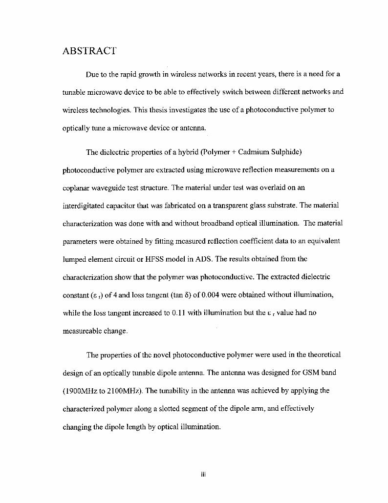
Due to the rapid growth in wireless networks in recent years, there is a need for a
tunable microwave device to be able to effectively switch between different networks and
wireless technologies. This thesis investigates the use of a photoconductive polymer to
optically tune a microwave device or antenna.
The dielectric properties of a hybrid (Polymer + Cadmium Sulphide)
photoconductive polymer are extracted using microwave reflection measurements on a
coplanar waveguide test structure. The material under test was overlaid on an
interdigitated capacitor that was fabricated on a transparent glass substrate. The material
characterization was done with and without broadband optical illumination. The material
parameters were obtained by fitting measured reflection coefficient data to an equivalent
lumped element circuit or HFSS model in ADS. The results obtained from the
characterization show that the polymer was photoconductive. The extracted dielectric
constant (e r) of 4 and loss tangent (tan d) of 0.004 were obtained without illumination,
while the loss tangent increased to 0.1 1 with illumination but the e r value had no
measureable change.
The properties of the novel photoconductive polymer were used in the theoretical
design of an optically tunable dipole antenna. The antenna was designed for GSM band
(1900MHz to 2100MHz). The tunability in the antenna was achieved by applying the
characterized polymer along a slotted segment of the dipole arm, and effectively
changing the dipole length by optical illumination.

ACKNOWLEDGEMENTS
Firstly, I am my grateful to my supervisors, Dr Langis Roy and Dr Barry Syrett
for the continuous technical support and guidance through the program. I also want to
appreciate my project group members, Atiff, Bashir, Greg, Arsalan, Popi for their
priceless contributions and ideas. Many thanks to the departmental staff, Blazenka,
Peggy, Sylvie and Anna for the moral support and care during the whole program.
Special thanks to Funmilayo Lawal for the time spent in editing, reference writing
and moral support. I am also extending my appreciations to Rhoda, Walefeips, Fola and
Femi, John for the moral and constant support
I would especially appreciate the Ogini's family who has made the whole
program a huge convenience.
My heartfelt gratitude goes to God, the author of wisdom, Who has held my hand
tightly throughout the ups and downs of this program.
IV
TABLE OF CONTENTS
ABSTRACT iii
ACKNOWLEDGEMENT iv
TABLEOFCONTENTS ?
LISTOFFIGURES vii
LISTOFTABLES xi
LIST OF ABBREVIATIONS AND SYMBOLS xii
CHAPTERl 1
Introduction 1
1.1 Motivation 1
1.2 Thesis Goals 2
1.3 Thesis Organization 3CHAPTER 2 5
Material Properties of Polymers and Applications to Tuning Microwave Devices 52.1 Introduction 5
2.2 Dielectric Properties ofMaterials 5
2.3 Optically Controllable Polymer 10
2.4 Tunable Microwave Device 15
2.5 Proposed Optical Tuning ofMicrowave components 22
2.6 Chapter Summary and Conclusion 24
CHAPTER 3 25
Characterization of a Novel Polymer 25
3.1 Introduction: Techniques and Proposed Method ofCharacterization 25
3.2 Monolithic Metal Insulator Metal (MIM) Capacitor 26
?
3.3 Interdigitateci Capacitor (IDC) 30
3.4 Development ofìnterdigitated Structurefor Polymer Characterization 32
3.5 Experimental Characterization ofNovel Polymer 39
3.6 Extraction and Modeling ofMaterial Properties 47
3.7 Chapter Summary and Conclusion 55
CHAPTER 4 57
Study of Optically Tunable Antenna 57
4.1 Tunable Dipole Antenna 57
4.2 Dipole Antenna Designfor GSM Band 62
4.3 Estimation ofthe Required Polymer Properties 724.4 Conclusion 75
CHAPTER 5 76
5.7 Conclusion 76
5.2 Future Work 77
REFERENCES 78
Vl
LIST OF FIGURES
Figure 2.1 Frequency dependence of permittivity for a hypotheticaldielectric 7
Figure 2.2 Electronic polarizations in material 8
Figure 2.3 Ionic polarizations showing the application of ?-Field 9
Figure 2.4 Dipolar polarization 9
Figure 2.5 Conductivities of various polymeric materials coveringthe conductivity span 11
Figure 2.6 PVK with the fullerene PCBM, 4F-TCNQ, TCNP 13
Figure 2.7 (a)-(e) Eplanationof photorefractive effect (a) Theabsorption of the light, (b) Transport of the chargecarriers, (c) Trapping of the carriers, (d) and (e) Dephasing 15
Figure 2.8 Common wireless usages for different applications 16
Figure 2.9 Configuration for the electrically controllable antennawith the voltage applied perpendicularly to the directionof the propagation 16
Figure 2.10 Measured antenna pattern at 7.8GHz as a result of bias voltage 18Figure 2.11 A single pole double throw RF MEMS switch 20
Figure 2.12 Dipole antenna with RF MEMS along the length of the arm 21Figure 2.13 Antenna pattern of the RF MEMS tunable dipole antenna 21
Figure 2.14 Tunable bandpass filter with its response overlaid withoptically sensitive polymer 22
Figure 2.15 Tunable bandpass filter with its response overlaid withoptically sensitive polymer upon illumination 23
Figure 3.1 Metal Insulator Metal (MIM) Capacitor 26Figure 3.2 Equivalent lumped element model MIM 27Figure 3.3 (a)The top view of HFSS model of CPW feed MIM capacitor 29Figure 3.3 (b) The side view of the model showing the "step" 29Figure 3.4 A two port interdigitated capacitor 30
vii
Figure 3.5 A lumped equivalent model of IDC. Rs, Ls and Csare the series resistor, inductor and capacitorrespectively. The Cp is the parallel capacitor 31
Figure 3.6 HFSS model of interdigitated capacitor with the zoomedsection showing the ??µ?? spacing between each fingers,where LF is the length of the Finger, WF is the width of thefinger, WFB is the width of the feedbar CPW, W is thewidth of the CPW, L is the length of CPW, LFB is the lengthof the feed bar, and G gap between groundand signal line (0.32µ???) 33
Figure 3.7 HFSS model of the material under test placed on interdigitatedcapacitor with 1mm finger length 35
Figure 3.8 (a) and (b). The Simulated Sl 1 on Smith chart for 1mm fingerlength interdigitated capacitor with lossy dielectric overlayhaving eG=5 over frequency range of100MHz to 5GHz with tanô as a parameter 36
Figure 3.9 The Simulated SIl for the 1mm finger lengthinterdigitated capacitor with lossy dielectricoverlay having eG=5 over frequency range of100MHz to 5GHz with tanô as a parameter 37
Figure 3.10 (a) and (b) The Simulated Phase of Sl 1 for the 1mmfinger length interdigitated capacitor with lossydielectric overlay having tanô =0.05 over frequencyrange of 1 00MHz to 5GHz with sr as a parameter 38
Figure 3.11 Fabricated IDC on a circular glass substrate 40
Figure 3.12 IDC with the new dimensions after fabrication 40
Figure 3.13 Characterization Setup showing the VNA, LAMPand the MUT 41
Figure 3.14 SIl measurements of the interdigitated from 100MHzto 5GHz with no overlay material. A) Shows theReturn loss, as the frequency increase lessreflection occurs. B) Phase. C) The capacitancewith resonance at 1.6GHz. D)SIl on Smith Chart 43
Figure 3.15 Mixture of CdS and polymer overlaid on theinterdigitated capacitor with SMA connectormounted with silver epoxy 44
VlIl
Figure 3.16 Measured results for IDC having a nominal fingerlength of- 1mm having CdS/polymer overlay coatingwith and without broadband optical illumination, withillumination over the frequency range of 100MHz to 5 GHz.
a) Return loss, b) Impedance on Smith chart, c) Phase of S 1 1 45
Figure 3.17 Lumped element equivalent circuits forthe connector, CPW and IDC 47
Figure 3.18 HFSS model for the fabricated modelwith MUT overlaid on the IDC 48
Figure 3.19 Equivalent lumped/HFF model with s-parameter(SP) data from HFSS 49
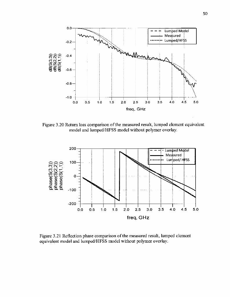
Figure 3.20 Return loss comparison of the measured result,lumped element equivalent model and lumped/HFSS modelwithout polymer overlay 50
Figure 3.21 Reflection phase comparison of the measured result,lumped element equivalent model and lumped/HFSS modelwithout polymer overlay 50
Figure 3.22 Return loss comparison of the measured result, lumpedelement equivalent model and lumped/HFSS model withpolymer overlay having er =4 and tan S = 0.004 - No illumination 52
Figure 3.23 Reflection phase comparison of the measured result, lumpedelement equivalent model and lumped/HFSS model withpolymer overlay having sr =4 and tan d = 0.004 - No illumination 52
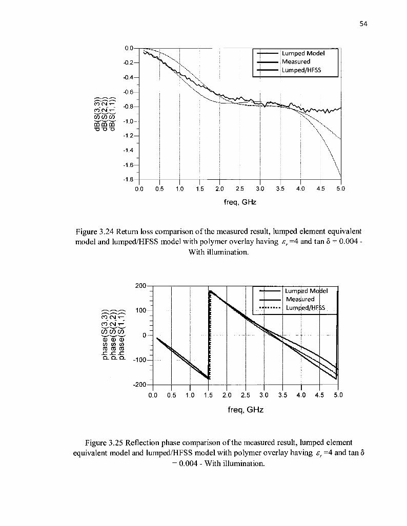
Figure 3.24 Return loss comparison of the measured result,lumped element equivalent model and lumped/HFSSmodel with polymer overlay having sr =4 andtan d = 0.004 - With illumination 54
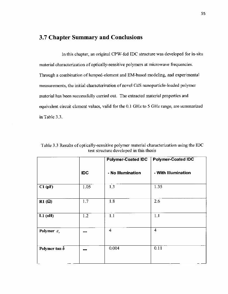
Figure 3.25 Reflection phase comparison of the measured result, lumpedelement equivalent model and lumped/HFSS model with polymeroverlay having er =4 and tan d = 0.004 - With illumination 54
Figure 4.1 Dipole arm with two diodes on each arm 58Figure 4.2 Measured return loss of multi-frequency dipole for, all
the diodes are OFF, inner diodes are ON, all diodes are ON 59
IX
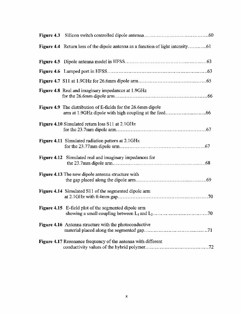
Figure 4.3 Silicon switch controlled dipole antenna 60
Figure 4.4 Return loss of the dipole antenna as a function of light intensity 61
Figure 4.5 Dipole antenna model in HFSS 63
Figure 4.6 Lumped port in HFSS 63
Figure 4.7 SIl at 1 .9GHz for 26.6mm dipole arm 65
Figure 4.8 Real and imaginary impedances at 1 .9GHzfor the 26.6mm dipole arm 66
Figure 4.9 The distribution of ?-fields for the 26.6mm dipolearm at 1 .9GHz dipole with high coupling at the feed 66
Figure 4.10 Simulated return loss Sl 1 at 2.1GHzfor the 23.7mm dipole arm 67
Figure 4.1 1 Simulated radiation pattern at 2. 1 GHzfor the 23 .77mm dipole arm 67
Figure 4.12 Simulated real and imaginary impedances forthe 23.7mm dipole arm 68
Figure 4.13 The new dipole antenna structure withthe gap placed along the dipole arm 69
Figure 4.14 Simulated SIl of the segmented dipole armat 2.1GHz with 0.4mm gap 70
Figure 4.15 ?-field plot of the segmented dipole armshowing a small coupling between Li and L2 70
Figure 4.16 Antenna structure with the photoconductivematerial placed along the segmented gap 71
Figure 4.17 Resonance frequency of the antenna with differentconductivity values of the hybrid polymer 72
?
LIST OF TABLES
Table 3.1 Properties of Corning 7059 27
Table 3.2 Different geometry of IDC with the corresponding Capacitance and SRF. . ..34
Table 3.3 Results of optically-sensitive polymer material characterizationusing the IDC test structure developed in this thesis 55
Table 4.1 The optimized length and spacing for the dipole antenna 64
Table 4.2 Resonance frequency with conductivity and the material type 74
Xl
LIST OF ABBREVIATIONS
GSM Group Special Mobile
VNA Vector network analyzer
ADS Agilent Advance Design System
PVC Polyvinyl chloride)
PVK Poly-N-vinylcarbozole
PCBM Phenyl-C61-Butyric-Acid-Methyl-Ester
TCNP Tetracyanopyrazinide Dimer Dianion
CdS Cadmium Sulphide
MEMS Micro Electro Mechanical Systems
MIM Metal-Insulator-Metal
IDC Interdigitated CapacitorMUT Material Under Test
CPW Co-Planar Wave guide
ITO Indium tin oxide
SDR Software Define Radio
CR Cognitive Radio
XIl
Chapter 1
Introduction
1.1 Motivation
Many mobile devices that are used today, such as global positioning systems
(GPS), cellular phone, personal digital assistants (PDA) operate on multiple wireless
networks, so there is a need for the devices to be able to effectively switch between these
different networks. This need has led to the development of tunable microwave devices.
The deployment of optically tunable microwave devices has become more attractive due
to its advantages over existing approaches such as tuning by temperature or applied dc
bias. Optical control offers advantages such as high isolation between the controlling
optical beam and controlled microwave signal, fast response, and high-power handling
capability. Immunity to electromagnetic interference and absence of mechanical controls,
which usually lead to noise, wear and tear, are the other advantages of optically
controlled devices. Passive microwave devices such as phase shifters, filters, attenuators,
antennas, switches can be controlled optically [1] [2] [3].
The principle behind the optical tunability of these devices is photo-excitation of a
photosensitive dielectric material. The photo-carriers in the dielectric material modulate
the complex dielectric constant changing the propagation characteristics of the
microwave signal. At low microwave frequencies the photo-carriers essentially modify
the conductance of the material keeping the dielectric constant of the medium practically
1
2
unaltered. However, at millimeter wavelengths, both the real and imaginary part of the
dielectric constant is modified due to photo-excitation. This effect makes it possible to
develop optically controlled microwave devices [2]. In some resonance circuit of
inductance (L) and capacitance (C), optical tunability is easily achieved because the
capacitance of a material is a function of the dielectric constant which can be altered as a
function of light illumination.
Polymers are organic materials. They are light in weight, cheap, non toxic, and
easy to manipulate. The material properties of some polymers can be altered by applying
external forces (applied dc field, excitation by light, pressure etc). The effect of the
change in the material properties can be used to tune or reconfigure microwave devices.
As part of the ongoing research Prof W.Wang of the chemistry department and Prof. S.
McGarry are currently developing new optically sensitive polymers at Carleton
University.
1.2 Thesis Goals
The major goal of this thesis research is to characterize a novel optically sensitive
polymer in the microwave region. That is, by the use of microwave measurements to
extract the basic physical properties of the polymer, namely dielectric constant, loss
tangent and the conductivity as a function of optical illumination. The second main goal
is to use this information to design an optically tunable dipole antenna at the GSM band
(1900MHz to 2100MHz).
3
The specific goals of this thesis are as follows.
1 . Develop a suitable test structure for microwave characterization of optically
sensitive polymers.
2. Extract and assess the material properties of the optically sensitive materials
under test
3 . Determine the conductivity ranges required of future generations of optically
controlled polymers.
4. Show the possible design of an optically-tunable microwave
antenna.
1.3 Thesis Organization
The first section of Chapter 2 gives basic details on dielectric properties of
materials and polarization in dielectric materials. Section 2.2 describes the properties and
applications of polymers. The photorefractive and photoconductive properties of
polymers are also reviewed in this section. Section 2.3 reviews the different types of
tunable microwave components related to our research, methods of tuning and the
limitations of these methods. The characterization of the hybrid polymer is discussed in
Chapter 3. The basic technique is to apply a photo-sensitive polymer on to a microwave
interdigital capacitor and measure the change in capacitance under optical illumination
using a vector network analyzer (VNA). Many different geometries of a tunable
interdigital capacitor were studied. The geometry, measured capacitance and the self-
resonant frequency of these capacitors with or without optical illumination are presented
in section 3.3. The modeling and the extraction of the properties of the material under test
4
were also investigated using commercially available software ANSOFT HFSS and
Agilent Advance Design System (ADS).
A tunable dipole antenna is designed in Chapter 4 based on the approximate
parameters that were extracted from the results in Chapter 3. The conductivity of the
material was used to change the resonant frequency of the antenna from 1900MHz to
2100MHz.
Chapter 5 gives a summary of the results and the work done in the thesis.
Opportunities for more research are also presented.
Chapter 2
Material Properties of Polymers and
Application to Tuning Microwave Devices.
2.1 Introduction.
Section 2.2 gives a background of dielectric properties of materials, the effect of
applications of strong electric field, and optically sensitive polymer and its applications.
Tunable microwave devices are discussed at the last Section, and different methods of
microwave tuning are reviewed.
2.2 Dielectric Properties of Materials.
Dielectric materials are substances with very low conductivity usually in the range
of 10"20 to 10"12 (Qm)"1. They are also known as insulators because the electrons arebound to the atomic nuclei by strong forces. They are very useful because of the electrical
polarization properties they exhibit. On applying electric field E to most dielectric
materials, the polarization of the atoms and molecules create a dipole moment P that
increases the displacement flux density/) [10]. The relationship between, D , E and P is
given as
5
6
D = e0? + P (2.1)
where e0 is the permittivity of free space.
In linear isotropic materials, the polarization of the dielectric materials relates to
the electric field by
P = S0XeE (2.2)
where ?e the is the electric susceptibility. Using Eqn. (2.2) in (2.1) gives
D = S0(I + ?ß (2.3)or
D = s0srE = sE (2.4)
where sr = 1 + xe is the relative permittivity, and e is the permittivity. The complex
permittivity can be written as
e = ?-]e? (2.5)
The real part £·' relates to the capability of the material to store electric energy. The
imaginary part e1 relates to the losses in the dielectric material, due to damping of
vibrating dipole moment or polarization loss [1O][I I]. Eqn. (2.6) expresses the loss
tangent of a good insulator,
e1tan d = ?-G (2.6)
If it is not a good insulator, the material may also have some conductor loss characterized
by conductivity s. The loss tangent including both polarization loss and conductor loss is
given by
tan d = ?e" +s?e
(2.7)
where ? = 2* p* f
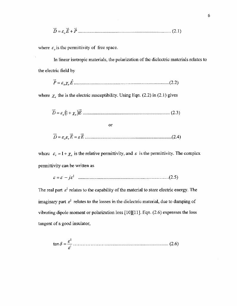
It has been reported that both the real £·' and the imaginary part £·" of the permittivity
depend on temperature, light intensity and pressure (piezoelectric effect) [5] [12]. There is
also strong frequency dependence of both real and imaginary part of the dielectric as
shown Figure 2.1. "e" generally decreases with increasing frequency, with perturbations
of this trend attributable to atomic and polarization effects.
ft
73
0
Dipolar and related relaxation phenomena
¦ ¦> '
10si-tr-.T
AtenúeElectronic
10* IQ9 101Î 10!M
Microwaves Miîlimeier Inftated Visible Ultravioletwaves
Frequency (Hz)
Figure 2.1 Frequency dependence of permittivity for a hypothetical dielectric
[10].
8
It can be seen that electronic polarization dominates at the optical frequency 1015Hz ,while atomic polarization peaks at 1012Hz which is between the millimeter range and theinfrared region. Both these effects alter the dielectric's properties (potentially useful for
microwave circuit tunability) and will be described in the next section.
2.2.1 Polarization in Dielectric.
Polarization in a dielectric is the process by which electric dipoles are formed or
aligned under the strong force of an electric field E . The different types of polarizations
are listed below [4] [5] [8] [9] [10]
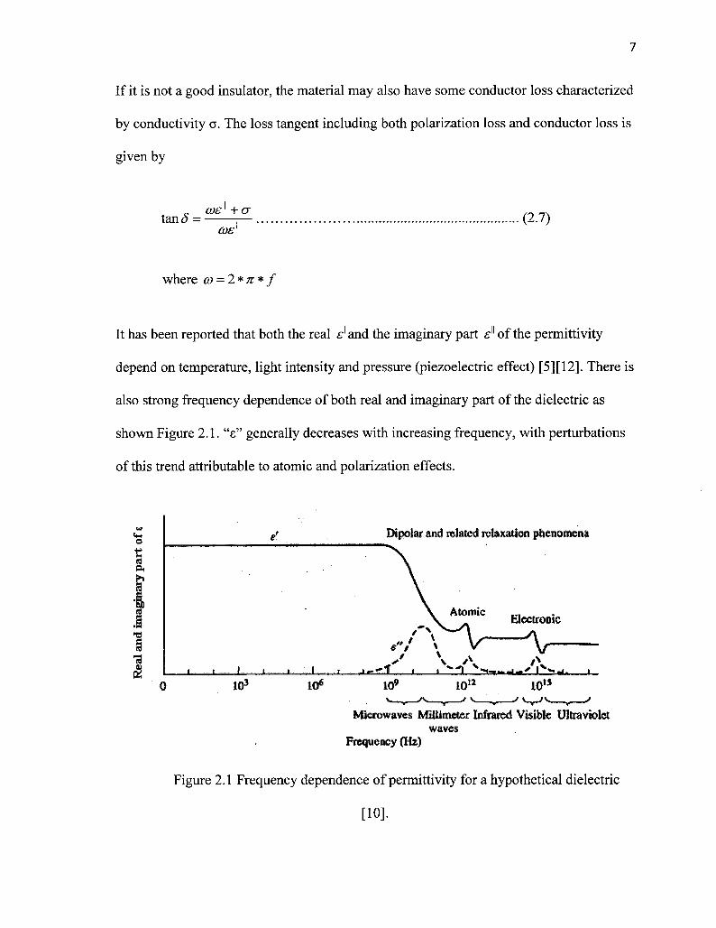
Electronic Polarization: This take place in neutral atoms. It occurs when an
electric field displaces the electron cloud surrounding the parent nucleus as shown
in Fig 2.2.
TT /
T
Figure 2.2 Electronic polarizations in
Atomic Polarization: It occurs when adjacent positive and negative ions stretch
under an applied electric field. Both electronic and atomic polarization are similar
[12].
9
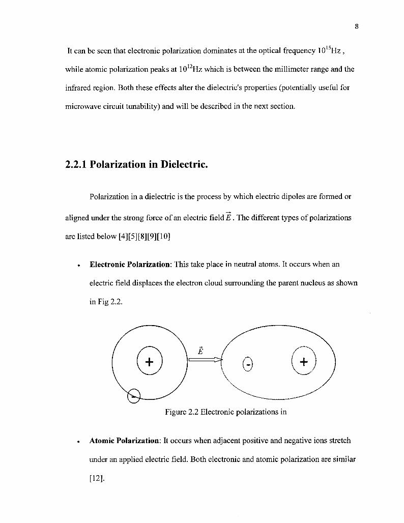
Ionic Polarization: Similar to atomic polarization, this involves the separation of
different ionic species under the influence of the applied electric fields as shown
in Figure 2.3 [10].
(+) \ O O \O \ © x0(?\
C-)±J (+/ © \X"-) /V <:-)(-) Qe-; aN ~\4"±; (+K OC^r:© N
\ ^ + /=^>\©-CJ ±){\ T\>v © 0 /
\ © O 0/¦ <± // \ /y\ / S
+)\ /X
Figure 2.3 Ionic polarizations showing the application of E-Field.
It is only found in ionic substances whose molecules are formed of atoms having
excess charges of opposite polarities [9]. The effect of ionic polarization usually
leads to a very high dielectric constant.
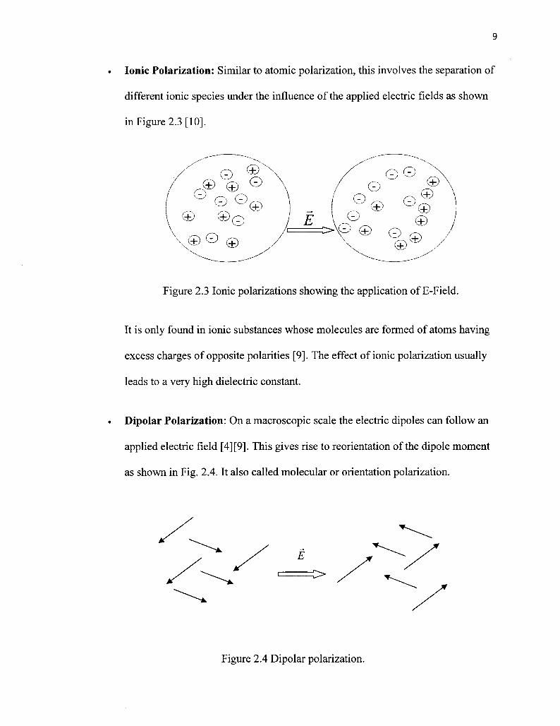
• Dipolar Polarization: On a macroscopic scale the electric dipoles can follow an
applied electric field [4] [9]. This gives rise to reorientation of the dipole moment
as shown in Fig. 2.4. It also called molecular or orientation polarization.
>
Figure 2.4 Dipolar polarization.
10
2.3 Optically Controllable Polymer.
Polymers are organic materials that are made from many molecules bonding
together to form a long molecular chain. Polymers are mostly used as insulating materials
because they possess strong covalent bonds. Polymers are readily available, cheap and
non-toxic. Polyethylene, Polypropylene, Polystyrene, Poly(vinyl chloride) (PVC),
Polytetrafluoroethylene (Teflon) are examples of polymers that are used in making
plastic bags, wire insulation, fibers, clear food wrap, video cassettes tape etc .
Polymers are now replacing inorganic materials in many applications because
some can have electrical properties that are very similar to semiconductors and metals
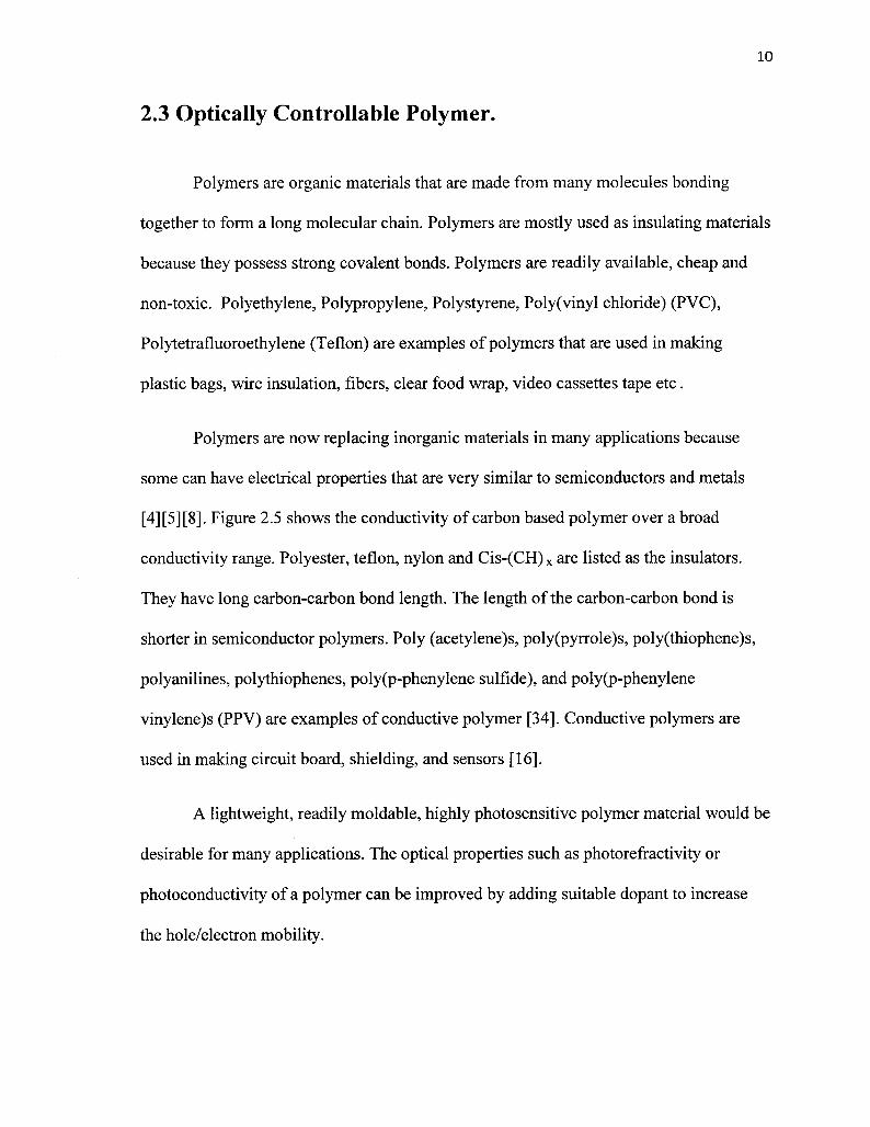
[4] [5] [8]. Figure 2.5 shows the conductivity of carbon based polymer over a broad
conductivity range. Polyester, teflon, nylon and Cis-(CH) x are listed as the insulators.
They have long carbon-carbon bond length. The length of the carbon-carbon bond is
shorter in semiconductor polymers. Poly (acetylene)s, poly(pyrrole)s, poly(thiophene)s,
polyanilines, polythiophenes, poly(p-phenylene sulfide), and poly(p-phenylene
vinylene)s (PPV) are examples of conductive polymer [34]. Conductive polymers are
used in making circuit board, shielding, and sensors [16].
A lightweight, readily moldable, highly photosensitive polymer material would be
desirable for many applications. The optical properties such as photorefractivity or
photoconductivity of a polymer can be improved by adding suitable dopant to increase
the hole/electron mobility.
11
\?a?/
Metals
Semi-conductors
Insu ators
IO6·
IO4
IO2
1
io-2
IO"4
io-6
io-8
io-10
io-12
IO-M.
IO"16
PolyacetyleneCopper"GrapRiiefÄsFs
_____ <?.%. ? PolyphenyleneDoped polypyrrole(CH)x: AsFs ^. poly (p-phenylene
Graphite . . ?Doped polyazulene vinylene) sDoped polyaniline
Trans (CH)x
Cis (CH)x
Nylon
Teflon
Polyester
Figure 2.5 Conductivities of various polymeric materials covering the conductivity span[5], [34].
2.3.1 Photoconductive Polymer.
Photoconductive materials are materials in which the conductivity s increases
when illuminated by light. Photoconductive polymers are typically very good insulators
in the absence of light. Upon light excitation, the holes and electrons that were initially
immobile move in response to an applied electric field and the material becomes
12
conductive [16]. The increase in conduction arises from an increase in the concentration
of charge carriers upon the absorption of photons. Eqn. (2.8) relates the conductivity of a
material as function of the mobility, magnitude and concentration of charge carrier:
s = ?(?µ,+?µ?) (2.8)
where s is conductivity, q is the electron charge, µß is electron mobility, µ? is hole
mobility, ? is the electron concentration and/? is the hole concentration.
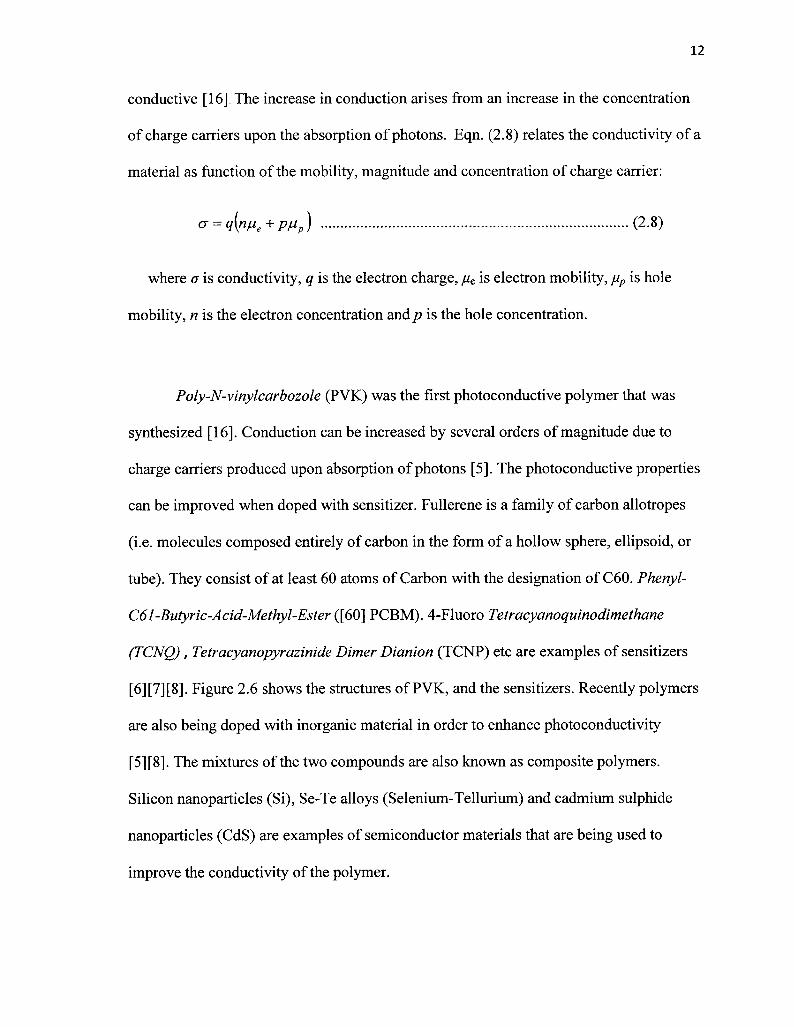
Poly-N-vinylcarbozole (PVK) was the first photoconductive polymer that was
synthesized [16]. Conduction can be increased by several orders of magnitude due to
charge carriers produced upon absorption of photons [5]. The photoconductive properties
can be improved when doped with sensitizer. Fullerene is a family of carbon allotropes
(i.e. molecules composed entirely of carbon in the form of a hollow sphere, ellipsoid, or
tube). They consist of at least 60 atoms of Carbon with the designation of C60. Phenyl-
C61 -Butyric-Acid-Methyl-Ester ([60] PCBM). 4-Fluoro Tetracyanoquinodimethane
(TCNQ) , Tetracyanopyrazinide Dimer Dianion (TCNP) etc are examples of sensitizers
[6] [7] [8]. Figure 2.6 shows the structures of PVK, and the sensitizers. Recently polymers
are also being doped with inorganic material in order to enhance photoconductivity
[5] [8]. The mixtures of the two compounds are also known as composite polymers.
Silicon nanoparticles (Si), Se-Te alloys (Selenium-Tellurium) and cadmium sulphide
nanoparticles (CdS) are examples of semiconductor materials that are being used to
improve the conductivity of the polymer.
13
OCH3 CN
V^n SXt>£HCNNC ¦?r CNNNC ^ /ZCNNC
CN
PVK PCBM 4F-TCNQ TCNP
Figure 2.6 PVK with the fullerene PCBM, 4F-TCNQ, TCNP.
Photogeneration of charge carriers and charge mobility in a polarization field are the
two areas in which the study of photoconductivity of polymers has been extensively
reviewed. They both contribute to the photoconductive properties independently [5].
Photogeneration of charge carriers depends on the wavelength of the incident photons. It
results from the separation of an electron from some chemical group leaving positively
charged holes. However, charge mobility results from the separation of holes and
electrons and the transfer of an electron from a neighboring neutral group to leave a
positive hole in the case of hole migration, or the transfer of an electron to a neighboring
neutral group in the case of electron migration [5][16].
2.3.2 Photorefractive Polymer.
Photorefractive polymers are special polymers that produce large refractive index
change upon exposure to light. The photorefractive effect refers to the field-induced
change in refractive index of an optical material, resulting from a light-induced
14
redistribution of electrons and holes [20]. Eqn. (2.9) shows the relationship between the
refractive index n, relative permittivity eG and permeability µG?? a material.
? = fi^ (2.9)
From Eqn. (2.9) a change in sr will change the refractive index n. The different steps
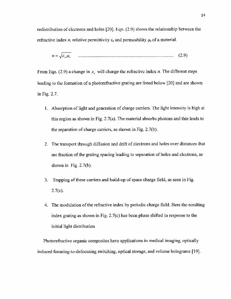
leading to the formation of a photorefractive grating are listed below [20] and are shown
in Fig. 2.7.
1 . Absorption of light and generation of charge carriers. The light intensity is high at
this region as shown in Fig. 2.7(a). The material absorbs photons and this leads to
the separation of charge carriers, as shown in Fig. 2.7(b).
2. The transport through diffusion and drift of electrons and holes over distances that
are fraction of the grating spacing leading to separation of holes and electrons, as
shown in Fig. 2.7(b).
3. Trapping of these carriers and build-up of space charge field, as seen in Fig.
2.7(c).
4. The modulation of the refractive index by periodic charge field. Here the resulting
index grating as shown in Fig. 2.7(e) has been phase shifted in response to the
initial light distribution
Photorefractive organic composites have applications in medical imaging, optically
induced focusing-to-defocusing switching, optical storage, and volume holograms [19].
15
Transport J±
Trapping /f$
Optical beam
Dephasing
Figure 2.7 (a)-(e) Eplanation of photorefractive effect (a) The absorption of the light, (b)Transport of the charge carriers, (c) Trapping of the carriers, (d) and (e) Dephasing [20].
2.4 Tunable Microwave Device.
The growth and the application of wireless technology have led to a need for a
single electronic device to be able to effectively switch between different networks and
wireless technologies. The possibility to use the same device for different applications is
the motivation for the development of tunable microwave devices. With the growth of
future wireless networks, there will be a crisis of spectrum availability under the current
16
spectrum allocation scheme. The IEEE body is working towards the effective spectrum
allocation sharing to avert the crisis [32]. The introduction of software-define radio
(SDR) and cognitive radio (CR) has help the regulating body to effectively manage and
share the spectrum effectively. SDR provides a flexible radio platform capable of
operating over a continuously set of commutations standard and modes without any
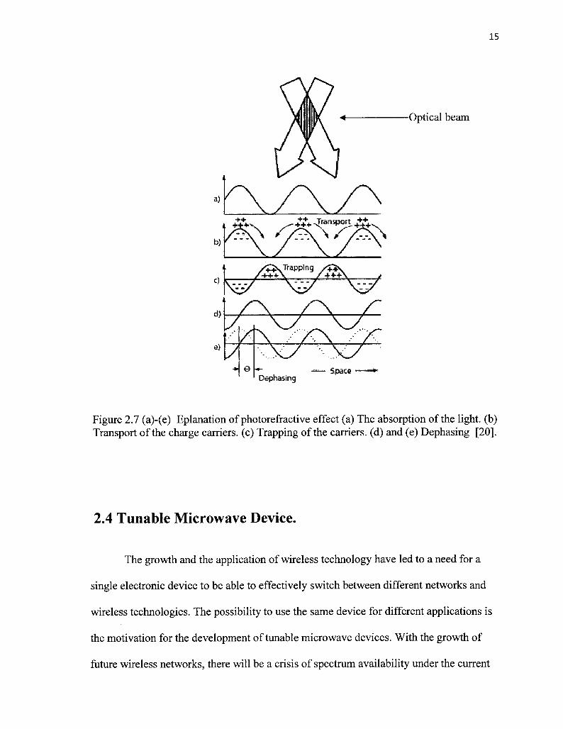
change in the hardware components [33], while it is been enable by the CR. Figure 2.8
shows different applications ofwireless devices relying on the same source for wireless
signals.
Internet
Antenna
r
Sentech'sMyWireless
Modem
fà ^
Firewall
Single AccessPoint with upto 253 Clients
Wireiess-GBroadband Router
(54-iOBMbps)
^
Voice over Internet
Protocol (VoIP phone)
&'
<TF
Wireless LANClient (PDA}
-^PWireless LANClient
Wireless LANClient
DatabaseServer
MultifunctionPrint/Copy/Scan/Fax
Figure 2.8 Common wireless usages for different applications.
Some other well known methods of tuning microwave devices are mechanical
tuning, magnetic tuning, variation of dc bias voltage, temperature, and Micro Electro
Mechanical Systems (MEMS).
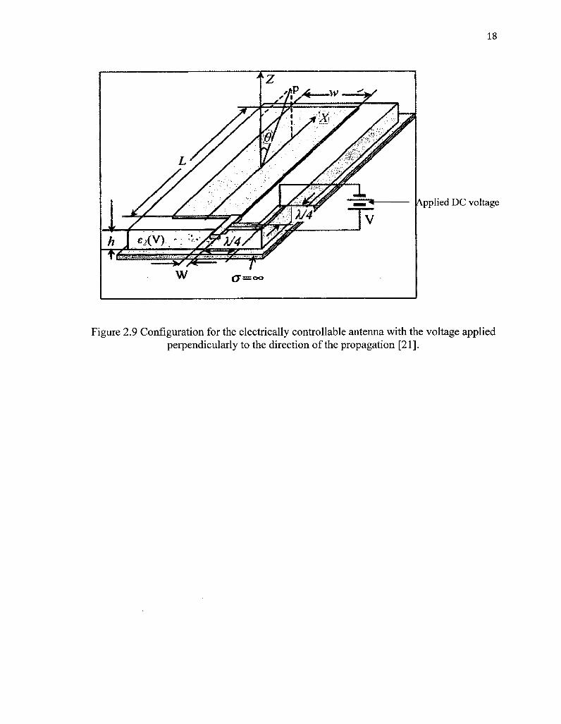
Ref. [21] studied the effect of tuning a microstrip travelling wave antenna by
applying a dc bias voltage. The principle behind the tunability is the property of
ferroelectric materials having a dielectric constant which can be modulated at high
frequencies under the effect of an electric field bias operating perpendicular to the
direction of propagation. Figure 2.9 shows the configuration of the electrically
controllable scan antenna. The antenna was made from a microstrip line with 200µ??
thick ceramic-polymer substrate. The antenna with width (w) 1 Omm and length (L) of
96mm is fed by a metal strip of width (W). The voltage is applied to the structure
perpendicular to the direction of propagation (ZOX) at the end of a ?/2 high impedance
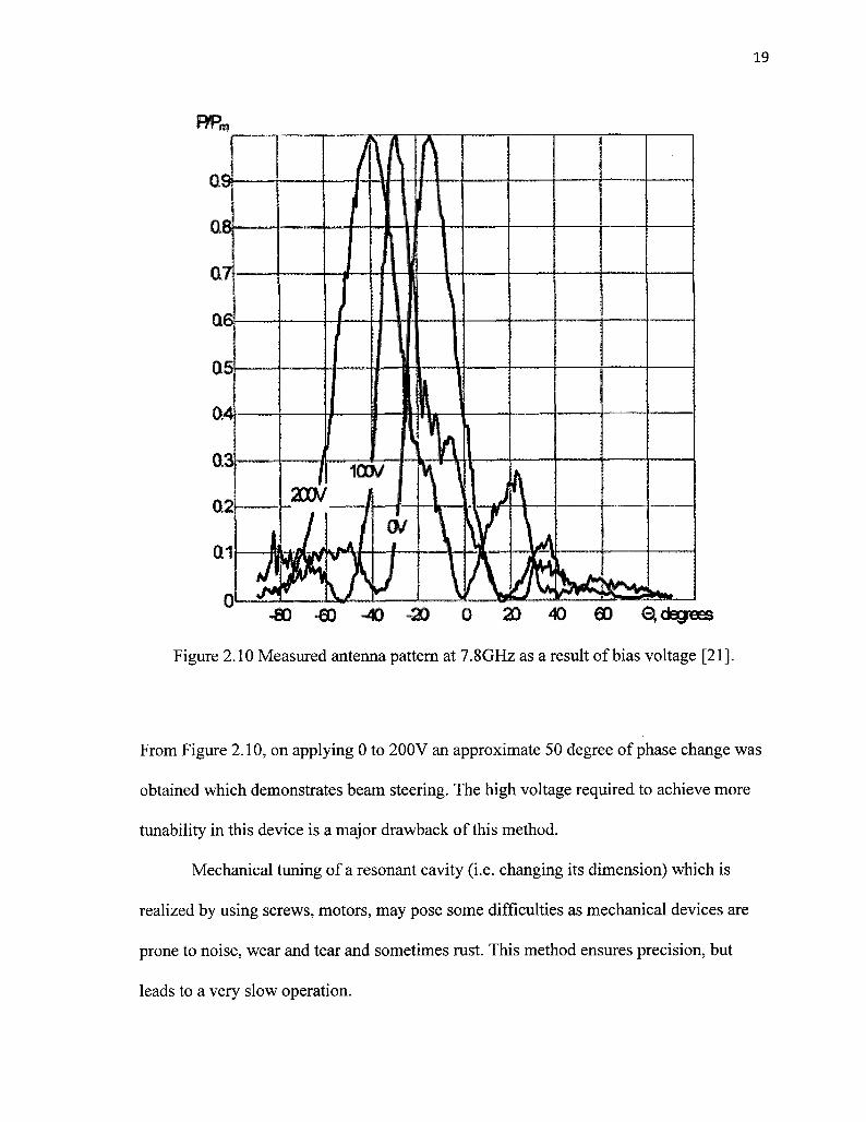
transmission line. The antenna pattern of scan measured at 7.8GHz with OV, 100V and
200V, is shown in Fig.2.10.
18
«XV). - ; ¦·'
applied DC voltage
Figure 2.9 Configuration for the electrically controllable antenna with the voltage appliedperpendicularly to the direction of the propagation [21].
19
•Ä) -€0 -40 -20 O a> 40 60 ^degnaes
Figure 2. 10 Measured antenna pattern at 7.8GHz as a result of bias voltage [21].
From Figure 2.10, on applying 0 to 200V an approximate 50 degree of phase change was
obtained which demonstrates beam steering. The high voltage required to achieve more
tunability in this device is a major drawback of this method.
Mechanical tuning of a resonant cavity (i.e. changing its dimension) which is
realized by using screws, motors, may pose some difficulties as mechanical devices are
prone to noise, wear and tear and sometimes rust. This method ensures precision, but
leads to a very slow operation.
20
Conventional electronic tuning element i.e. varactors, pin diodes, are seriously
limited by nonlinear effects, leading intermodulation products and low power handling
capabilities [H]. MEMS technology can also be used to tune a microwave component.
High power handling, low intermodulation distortion and very small size are the
attractive features offered by MEMS [24]. MEMS devices require careful fabrication and
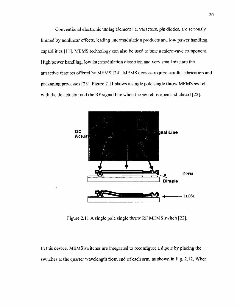
packaging processes [23]. Figure 2.1 1 shows a single pole single throw MEMS switch
with the dc actuator and the RF signal line when the switch is open and closed [22].
nal UneActúa
Dimple
OPEN
CLOSE
Figure 2.1 1 A single pole single throw RF MEMS switch [22].
In this device, MEMS switches are integrated to reconfigure a dipole by placing the
switches at the quarter wavelength from end of each arm, as shown in Fig. 2.12. When
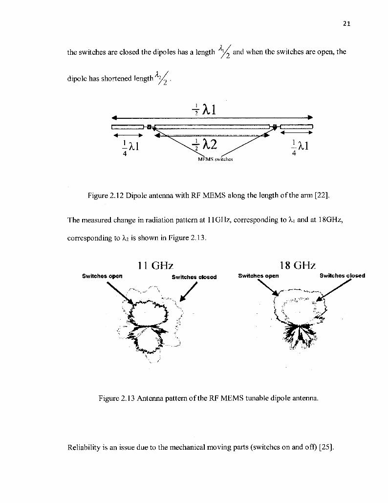
21
?,the switches are closed the dipoles has a length yL and when the switches are open, the
?,dipo le has shortened length 2/
t??ET¦,„-„¦¦ ---. ¦ .-,!""IBfa^
???4
?2 ???MEMS switches
Figure 2.12 Dipole antenna with RF MEMS along the length of the arm [22].
The measured change in radiation pattern at 1 IGHz, corresponding to ?? and at 18GHz,
corresponding to Xi is shown in Figure 2.13.
1 1 GHzSwitches open Switches closed
/1
1 8 GHzSwitches open Switches closed
?
Figure 2.13 Antenna pattern of the RF MEMS tunable dipo Ie antenna.
Reliability is an issue due to the mechanical moving parts (switches on and off) [25].
22
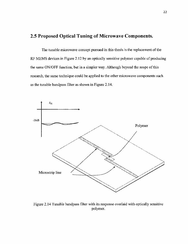
2.5 Proposed Optical Tuning of Microwave Components.
The tunable microwave concept pursued in this thesis is the replacement of the
RF MEMS devices in Figure 2.12 by an optically sensitive polymer capable of producing
the same ON/OFF function, but in a simpler way. Although beyond the scope of this
research, the same technique could be applied to the other microwave components such
as the tunable bandpass filter as shown in Figure 2.14.
-2OdB
Polymer
\
Microstrip line
Figure 2.14 Tunable bandpass filter with its response overlaid with optically sensitivepolymer.
23
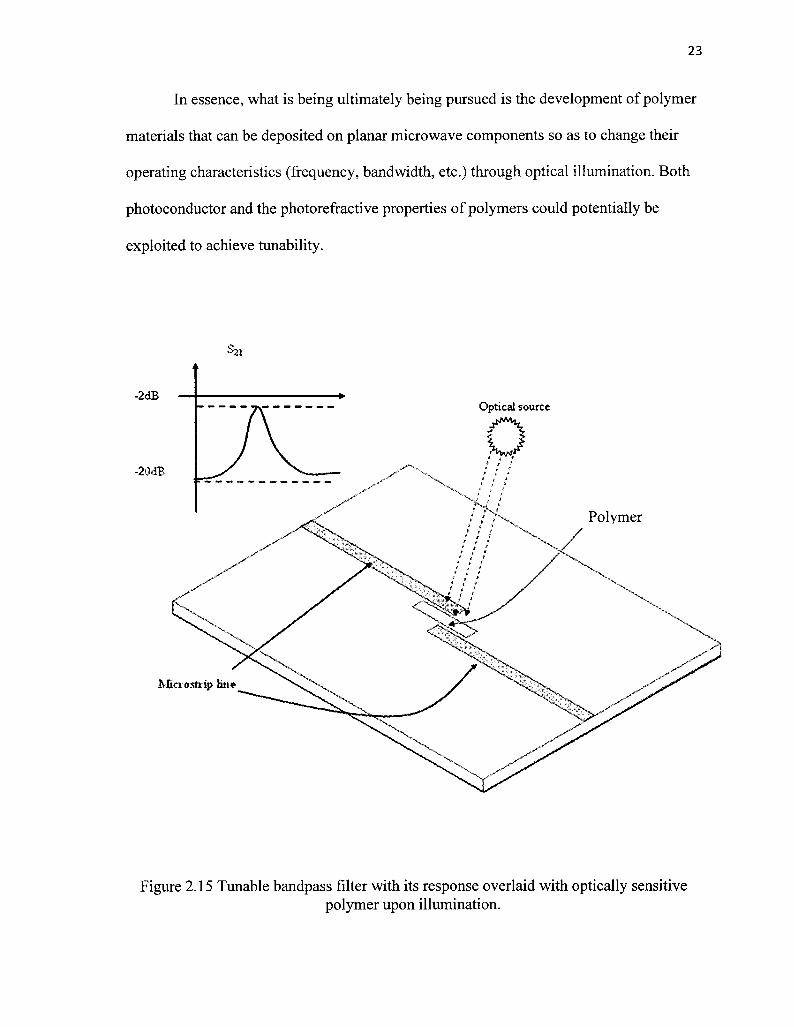
In essence, what is being ultimately being pursued is the development of polymer
materials that can be deposited on planar microwave components so as to change their
operating characteristics (frequency, bandwidth, etc.) through optical illumination. Both
photoconductor and the photorefractive properties of polymers could potentially be
exploited to achieve tunability.
-2dB ?Optical source
???^t2OdB N
¿fs> Polymer
^*
x-/ ?«
s X/ Í
^-
^ ^Mei ostri» one
\ /
x*
Figure 2.15 Tunable bandpass filter with its response overlaid with optically sensitivepolymer upon illumination.
24
2.6 Chapter Summary and Conclusions
The dielectric properties of material were reviewed; the photoconductive and
photorefractive properties of polymer were described with applications. Tunable
microwave devices and different methods of tuning such as mechanical tuning, magnetic
tuning, variation of dc bias voltage, temperature, and Micro Electro Mechanical Systems
(MEMS) were also described. The proposed method of optical tuning in this work was
also introduced.
Chapter 3
Characterization of a Novel Polymer.
3.1 Introduction: Techniques and Proposed Method of
Characterization.
The properties of a material must be known before it can be applied to a passive
microwave device to achieve tunability. The process by which the properties of a material
are determined is called characterization. The reflection method, the transmission
method, the resonator method, the resonant-perturbation method are different methods to
characterize a material at microwave frequencies [10].
In this chapter, the reflection method will be used for the material
characterization of planar microwave capacitors. A capacitor made with the polymer
material under test is a useful structure for performing the characterization work in the
thesis. First the material properties can be extracted fairly easily from the measured
impedance of the capacitor and, second the capacitor itself could be used directly as a
tuning element in a microwave circuit or antenna with precise knowledge of its behavior
having been determined. Such an approach is called "in-situ" material characterization. In
the reflection method, an electromagnetic wave is directed to the material under test, and
the parameters of interest are extracted from the reflection coefficient defined at the
reference plane [10]. A Vector network analyzer (VNA) can be used to measure the
reflection coefficient SIl. Initially a metal-insulator-metal (MIM) capacitor was
25
26
proposed as the test device, but due to the fabrication constraints an interdigitated
capacitor (IDC) was finally used. The substrate used for the planar microwave capacitor
must be optically transparent so the material under test (MUT) can be illuminated by
light. For this reason Corning 7059 glass (Barium Borosilicate) was used for the
substrate. Table 3.1 shows its physical properties obtained from [31]. The IDC will be fed
with a co-planar wave-guide (CPW), so as to allow the IDC and the MUT to be on the
same plane. This allows the light to get to the MUT without being blocked by the ground
plane.
3.2 Monolithic Metal Insulator Metal (MIM) Capacitor.
By measuring the impedance of a MIM, the dielectric constant and the loss
tangent of a material can be extracted [27]. The MIM is constructed by sandwiching a
thin dielectric material, the MUT, between two metal plates as shown in Figure 3.1 .
< METAL
^ INSULATOR (MUT)
4 METAL
/
Figure 3.1 Metal Insulator Metal (MIM) Capacitor
Table 3.1 Properties of Corning 7059 Substrate [31].
Properties Value
Density 2.76g/cmJ
Refractive Index
1.5440 @435.8nm
1.5354 @ 546. Inni
1.5311 @643.8nm
5.84 (a) lMHz/20°CDielectric constant
Loss Tangent 0.10%@lMHz/20uC
Transmittance
~70%(320nm)
~90%(360nm)
>90%(380-2200nm)
The electrical lumped element equivalent circuits of a MIM is shown in Fig
R LBO—VW—"^^^
h
G
Figure 3.2 Equivalent lumped element model MIM.
28
The notation B and T represent the bottom and the top plate of the capacitor, respectively.
The parameters Resistance (R), Inductance (L), Capacitance (C), and Conductance (G)
can be approximated with Eqns. (3.1), (3.2) and (3.3) [26].
R=I^l (O) ....(3.1)3 W
C = ß? m. . Î^lL™ {F) (3.2)° rd d 36p d y '
G = coCtanô = —srdf — xlO-6tanô (mho) (3.3)Io U
where Rs is the sheet resistance of the bottom plate, srd, and tanô are the dielectric
constant and the lost tangent of the material under test, respectively. The length /, width
W and depth das shown in Figure 3.1 are in micrometers, and the frequency fis in GHz.
For optical characterization, one of the conducting layers must be transparent.
Indium tin oxide (ITO) which is a transparent metal was considered as the lower layer.
The idea was to coat the surface of the glass with ITO, deposit the polymer, and then coat
the top surface with aluminum. Figure 3.3(a) shows the top view of the structure with the
material under test modeled in Ansoft HFSS with ITO coated on the glass substrate. The
CPW is a 50O line having a center conductor (signal) S with a width of 2mm and spacing
(gap) G to the adjacent ground of 0.32mm.
29
< - GKD (ITO)« MUT
PLATE (Aluminum)
CPW Feed Line
Test Port
Figure 3.3(a) The top view of HFSS model of CPW fed MIM capacitor.
Test Port
—Test Plate (Aluminum)^ ITO
Coming 7059
MUX
Step
Figure 3.3(b) The cross-sectional view of the model showing the "step".
An extra step of coating the top surface of the glass with ITO must be done. ITO is also
known to be very lossy at microwave frequencies due to its low conductivity. In addition,
there is a vertical step from the aluminum CPW feed line to the aluminum top plate of the
capacitor over the MUT, as shown in Fig.3.3 (b). At microwave frequencies, accounting
30
for this discontinuity poses a major challenge while extracting the material properties.
Hence, the MIM capacitor was not used as the test structure.
3.3 Interdigitated Capacitor (IDC).
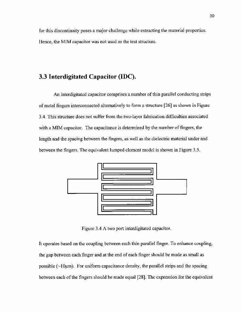
An interdigitated capacitor comprises a number of thin parallel conducting strips
of metal fingers interconnected alternatively to form a structure [26] as shown in Figure
3.4. This structure does not suffer from the two-layer fabrication difficulties associated
with a MIM capacitor. The capacitance is determined by the number of fingers, the
length and the spacing between the fingers, as well as the dielectric material under and
between the fingers. The equivalent lumped element model is shown in Figure 3.5.
Figure 3.4 A two port interdigitated capacitor.
It operates based on the coupling between each thin parallel finger. To enhance coupling,
the gap between each finger and at the end of each finger should be made as small as
possible (~10µ??). For uniform capacitance density, the parallel strips and the spacing
between each of the fingers should be made equal [28]. The expression for the equivalent
model elements of Fig. 3.5 are more complicated than for a MIM capacitor, An
electromagnetic simulation is preferred to determine the values of each element.
*—Wv
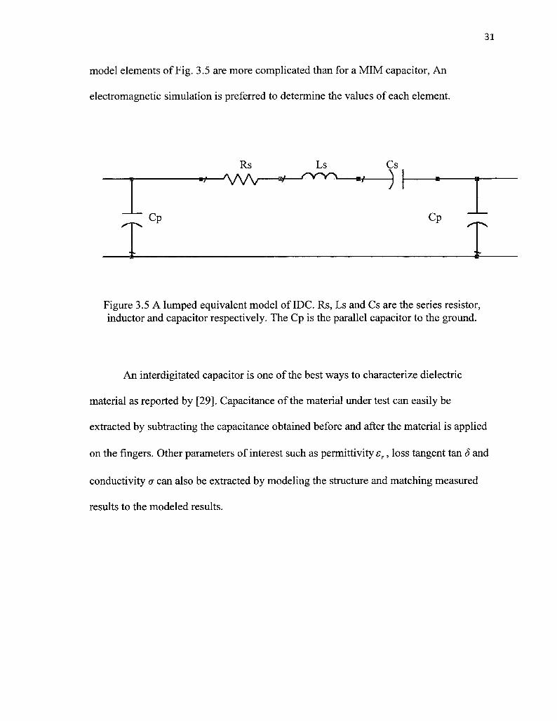
Figure 3.5 A lumped equivalent model of IDC. Rs, Ls and Cs are the series resistor,inductor and capacitor respectively. The Cp is the parallel capacitor to the ground.
An interdigitated capacitor is one of the best ways to characterize dielectric
material as reported by [29]. Capacitance of the material under test can easily be
extracted by subtracting the capacitance obtained before and after the material is applied
on the fingers. Other parameters of interest such as permittivity sr , loss tangent tan d and
conductivity s can also be extracted by modeling the structure and matching measured
results to the modeled results.
32
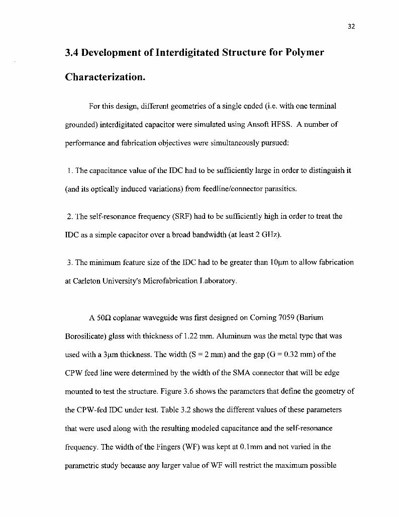
3.4 Development of Interdigitated Structure for Polymer
Characterization.
For this design, different geometries of a single ended (i.e. with one terminal
grounded) interdigitated capacitor were simulated using Ansoft HFSS. A number of
performance and fabrication objectives were simultaneously pursued:
1 . The capacitance value of the IDC had to be sufficiently large in order to distinguish it
(and its optically induced variations) from feedline/connector parasitics.
2. The self-resonance frequency (SRF) had to be sufficiently high in order to treat the
IDC as a simple capacitor over a broad bandwidth (at least 2 GHz).
3. The minimum feature size of the IDC had to be greater than ??µ?? to allow fabrication
at Carleton University's Microfabrication Laboratory.
A 50O coplanar waveguide was first designed on Corning 7059 (Barium
Borosilicate) glass with thickness of 1 .22 mm. Aluminum was the metal type that was
used with a 3µ?? thickness. The width (S = 2 mm) and the gap (G = 0.32 mm) of the
CPW feed line were determined by the width of the SMA connector that will be edge
mounted to test the structure. Figure 3.6 shows the parameters that define the geometry of
the CPW-fed IDC under test. Table 3.2 shows the different values of these parameters
that were used along with the resulting modeled capacitance and the self-resonance
frequency. The width of the Fingers (WF) was kept at 0.1mm and not varied in the
parametric study because any larger value of WF will restrict the maximum possible
numbers of fingers (NF) and a smaller value of WF would lead to inefficiency
GROUND
I !
Ll
Figure 3.6 HFSS model of interdigitatec
i
t
?
¡<tHi
4
H
<y
. WF
- LF
- LFB
- WFB
- L
?
setween each fingers, where LF is the length of the Finger, WF is the
"CPW (2mm), LFB (0.5mm) is the length of the feed bar,:tween :
It was observed that as length (LF) of the fingers increases, while keeping the number >
us (NF
;ases. F: in Table 3.
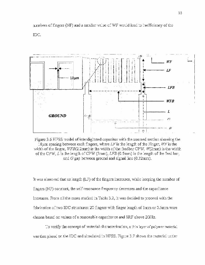
To verify the concept of material characterization, a thin
su placed on the IDC and simulated in HFSS. Figure 3.7 s
were
34
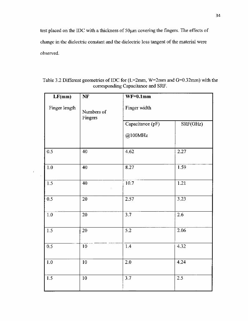
test placed on the IDC with a thickness of 50µ?? covering the fingers. The effects of
change in the dielectric constant and the dielectric loss tangent of the material were
observed.
Table 3.2 Different geometries of IDC for (L=2mm, W=2mm and G=O.32mm) with thecorresponding Capacitance and SRF.
LF(mm)
Finger length
0.5
1.0
1.5
0.5
1.0
1.5
0.5
1.0
1.5
NF
Numbers ofFingers
40
40
40
20
20
20
10
10
10
WF=0.1mm
Finger width
Capacitance (pF)
@100MHz
??2
"8^27
TÖ/7
2.57
3.7
5.2
1.4
2.0
3.7
SRF(GHz)
2.27
1.59
1.21
3.23
2.6
2.06
4.32
4.24
2.5
Jt JTMaterial under Test
? - * A - # - ?WEm
# . « , . * . *
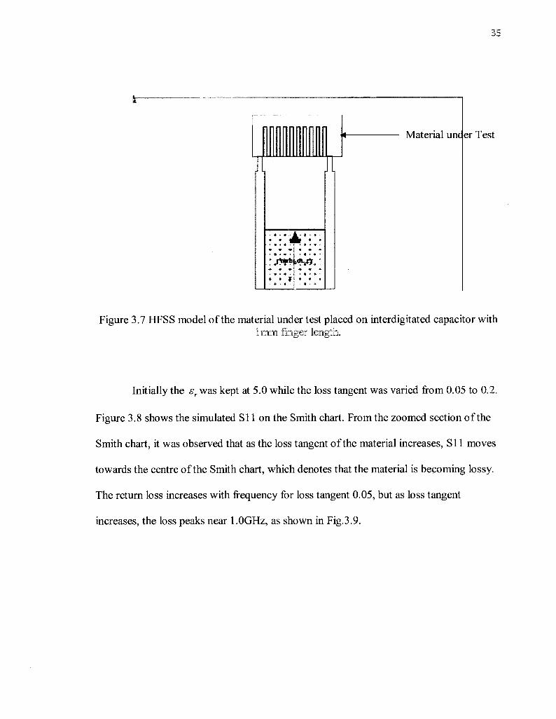
Figure 3.7 HFSS model of the material under test placed on interdigitated capacitor with1 mm finger length.
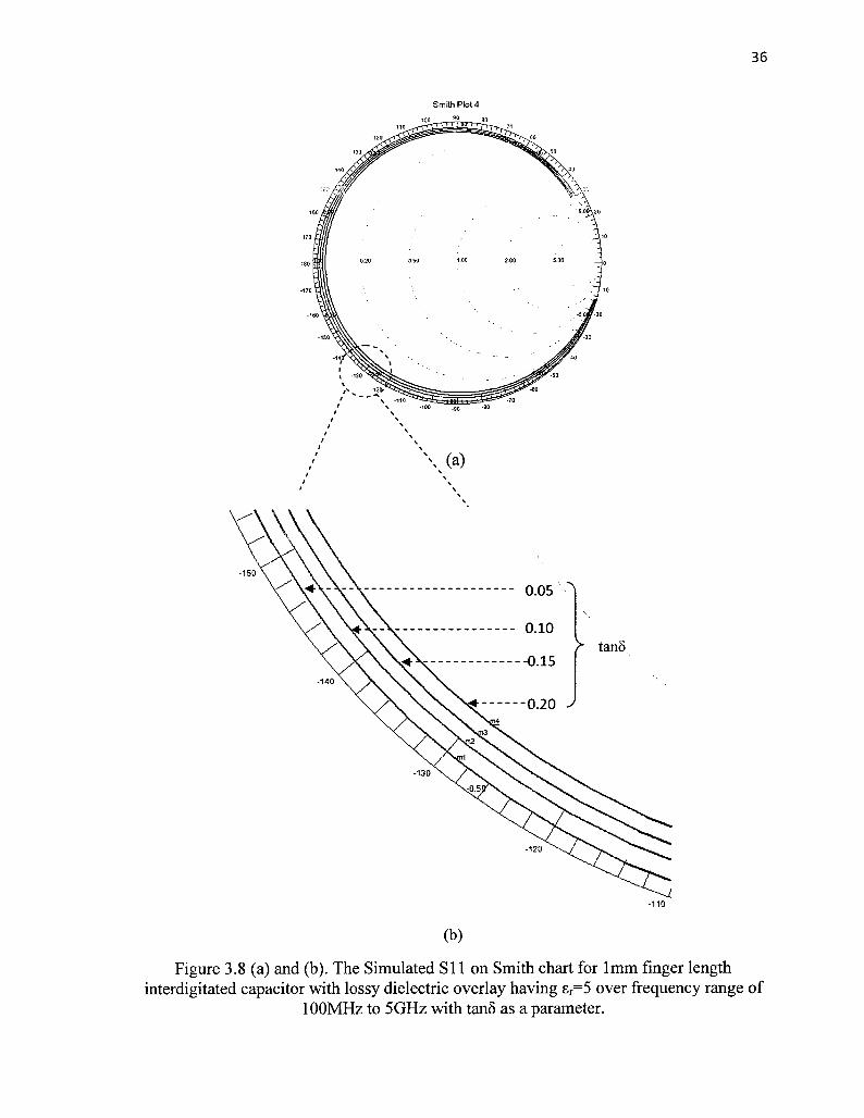
Initially the srwas kept at 5.0 while the loss tangent was varied from 0.05 to 0.2.
Figure 3.8 shows the simulated Sl 1 on the Smith chart. From the zoomed section of the
Smith chart, it was observed that as the loss tangent of the material increases, Sl 1 moves
towards the centre of the Smith chart, which denotes that the material is becoming lossy.
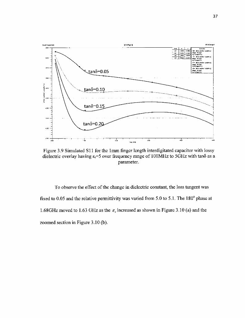
The return loss increases with frequency for loss tangent 0.05, but as loss tangent
increases, the loss peaks near 1.0GHz, as shown in Fig.3.9.
Smith Pot 490ICO GO
70110
60120
50130
40140
160
10170
1.00 2.00 OO0.20 0.50180
10170
20160
150 30
40
(50130
-602>
70110OO -8090
\ (a)
150
0.05 ì
0.10> tanô
0.15140
0.20 J
1
130
120
-110
(b)
Figure 3.8 (a) and (b). The Simulated Sl 1 on Smith chart for 1mm finger lengthinterdigitated capacitor with lossy dielectric overlay having sr=5 over frequency range
100MHz to 5GHz with tanô as a parameter.
37
Anso» Corporation XY p|0t 8 HFSSDesignl000
(ßa L imftrt 1 . Limrtni)5ttie1 ^hI4391»&»? ItMi-OCS'
6275O- «{SfLiiiiiRjrtUimftirtl))
m» 081B7Setiei : Sw eoe1IB=? Manico
(SI S(Limftrt1 . Lintftrtl»SetiBi : SwnplIB=1S ????^0 15
<£(?(??pt???? , Lurpftirtl))
tanô=0.05 Sensi : SweeplIB=1SIQrKf=O?
tanô=0.10 o
50
tanö=0.15-060
70
tanô=0.2-oso
-0 905 00002.00 3 00000 00
Freo GHz]
Figure 3.9 Simulateci SII for the lmm finger length interdigitated capacitor with lossydielectric overlay having eG=5 over frequency range of 100MHz to 5GHz with tanô as a
parameter.
To observe the effect of the change in dielectric constant, the loss tangent was
fixed to 0.05 and the relative permittivity was varied from 5.0 to 5.1. The 180° phase at
1.68GHz moved to 1.63 GHz as the et increased as shown in Figure 3.10 (a) and the
zoomed section in Figure 3.10 (b).
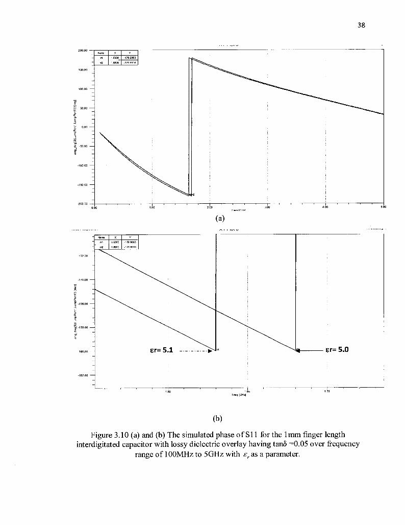
38
(a)
E -176.00
sr= 5.0sr=5.1 ?
Freq [GH 4
(b)
Figure 3.10 (a) and (b) The simulated phase of Sl 1 for the 1mm finger lengthinterdigitated capacitor with lossy dielectric overlay having tanô =0.05 over frequency
range of 100MHz to 5GHz with S1. as a parameter.
39
3.5 Experimental Characterization of Novel Polymer.
In this section, a mixture of thermoplastic (polymer) and nano-particles of
Cadmium Sulphide (CdS) was characterized (composite polymer) with the use of the two
fabricated IDC test structures developed. The thermoplastic used was DuPont 3571
proprietary polymer and its properties were not known. CdS is known to be an inorganic
semiconductor with photoconductive properties. CdS typically has a relative permittivity
of about 8 and a very high loss tangent. The fabricated wafer, measurement setup,
measurement procedure and the extraction of the material properties will be discussed.
3.5.1 Fabricated IDC Test Wafer.
The interdigitated capacitors were laid out with L-Edit, a commercial layout
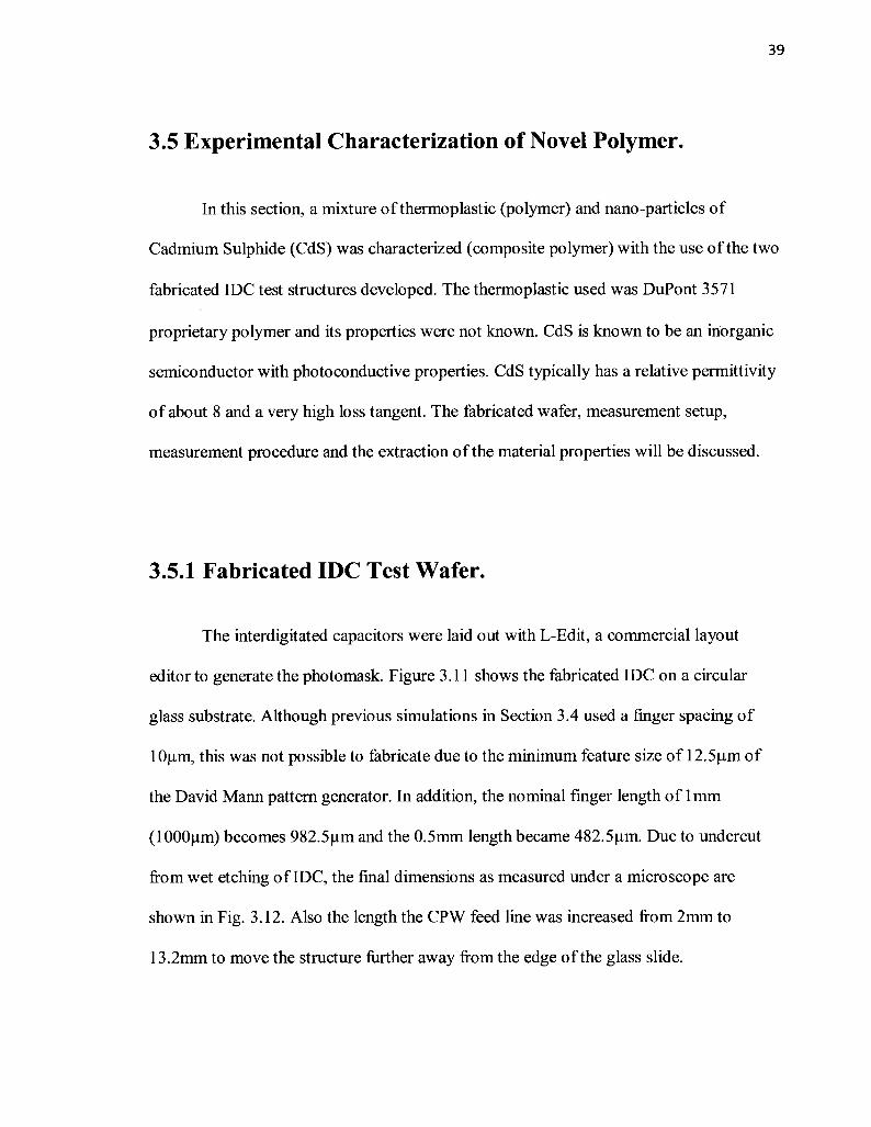
editor to generate the photomask. Figure 3.11 shows the fabricated IDC on a circular
glass substrate. Although previous simulations in Section 3.4 used a finger spacing of
1 ?µ?t, this was not possible to fabricate due to the minimum feature size of 1 2.5µ?? of
the David Mann pattern generator. In addition, the nominal finger length of 1mm
(????µ?t?) becomes 982. 5µ?? and the 0.5mm length became 482.5µ??. Due to undercut
from wet etching of IDC, the final dimensions as measured under a microscope are
shown in Fig. 3.12. Also the length the CPW feed line was increased from 2mm to
13.2mm to move the structure further away from the edge of the glass slide.
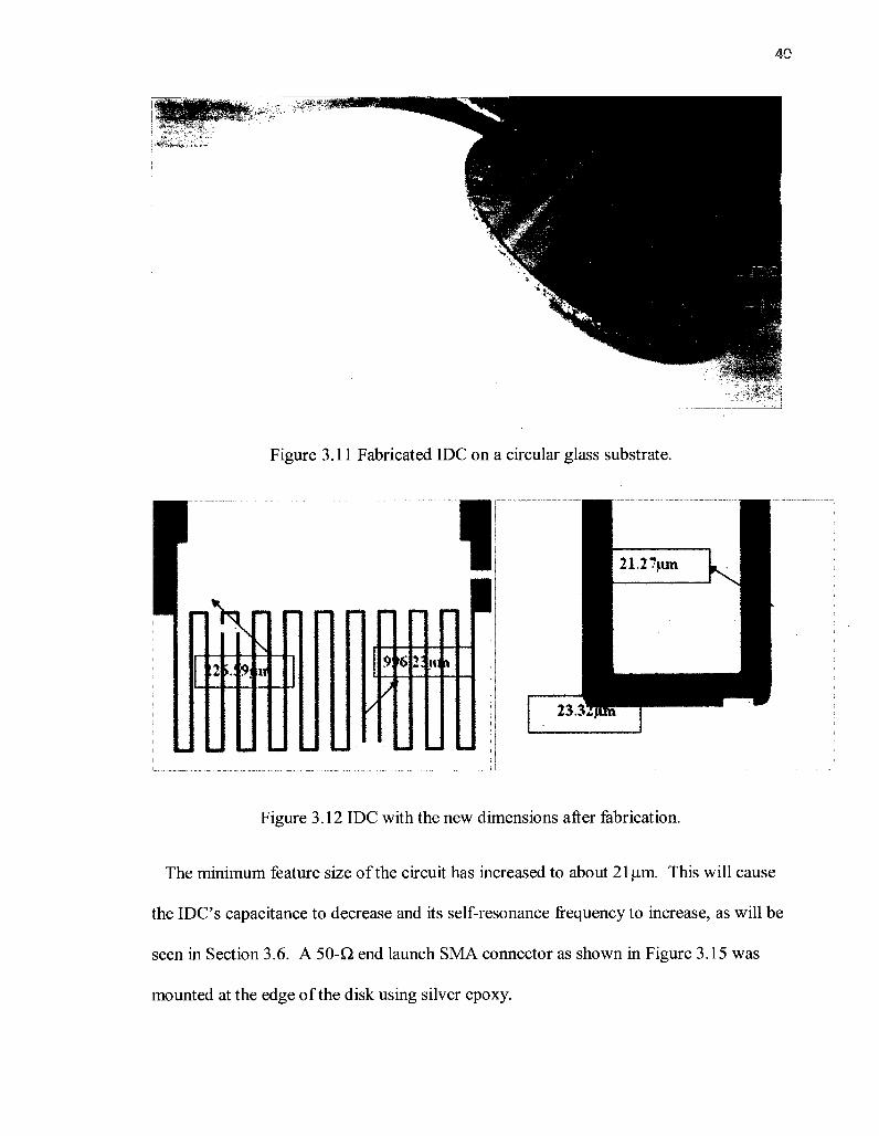
;jS*í
Figure 3.1 1 Fabricated IDC on a circular glass substrate.
1t2»
Hj9M
Nm
W">í 111)
21.2?µ??
Figure 3.12 IDC with the new dimensions after fabrication.
The minimum feature size of the circuit has increased to about 21µp?. This will cause
the IDC's capacitance to decrease and its self-resonance frequency to increase, as will be
seen in Section 3.6. A 50-O end launch SMA connector as shown in Figure 3.15 was
mounted at the edge of the disk using silver epoxy.
41
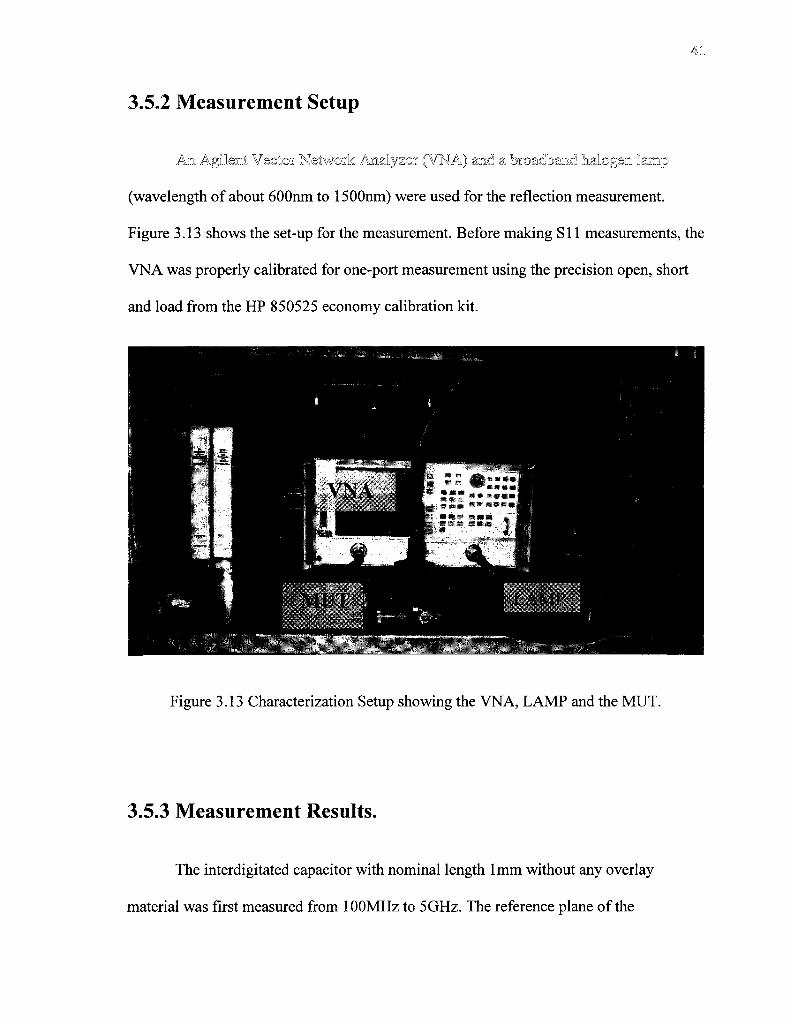
3.5.2 Measurement Setup
An Agilent Vector Network Analyzer (VNA) and a broadband halogen lamp
(wavelength of about 600nm to 1500nm) were used for the reflection measurement.
Figure 3.13 shows the set-up for the measurement. Before making SIl measurements, the
VNA was properly calibrated for one-port measurement using the precision open, short
and load from the HP 850525 economy calibration kit.
HjP"
4b\WÊÎÊ^m?:
PImmm mmm 1»
LAMPMlJT
¦^aíf^W»
Figure 3.13 Characterization Setup showing the VNA, LAMP and the MUT.
3.5.3 Measurement Results.
The interdigitated capacitor with nominal length 1mm without any overlay
material was first measured from 100MHz to 5GHz. The reference plane of the
42
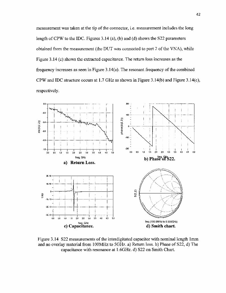
measurement was taken at the tip of the connector, i.e. measurement includes the long
length of CPW to the IDC. Figures 3.14 (a), (b) and (d) shows the S22 parameters
obtained from the measurement (the DUT was connected to port 2 of the VNA), while
Figure 3.14 (c) shows the extracted capacitance. The return loss increases as the
frequency increases as seen in Figure 3.14(a). The resonant frequency of the combined
CPW and IDC structure occurs at 1.7 GHz as shown in Figure 3.14(b) and Figure 3.14(c),
respectively.
0.0 0.5 1.0 1.5 2.0 2.5 3.0 3.5 4.0 4.5 5.0
freq, GHz
a) Return Loss.
?—?—?—?—? i ? r.0 0.5 1.0 1.5 2.0 2.5 3.0 3.5 4.0 4.5 5.0
freg, GHzc) Capacitance.
b)Phaseqo¥S22.
freq (100.0MHz to 5.000GHz)d) Smith chart.
Figure 3.14 S22 measurements of the interdigitated capacitor with nominal length 1mmand no overlay material from 100MHz to 5GHz. a) Return loss, b) Phase of S22, d) The
capacitance with resonance at 1 .6GHz. d) S22 on Smith Chart.
43
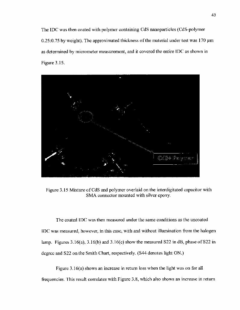
The IDC was then coated with polymer containing CdS nanoparticles (CdS-polymer
0.25:0.75 by weight). The approximated thickness of the material under test was 170 µ?t?
as determined by micrometer measurement, and it covered the entire IDC as shown in
Figure 3.15.
Figure 3.15 Mixture of CdS and polymer overlaid on the interdigitated capacitor withSMA connector mounted with silver epoxy.
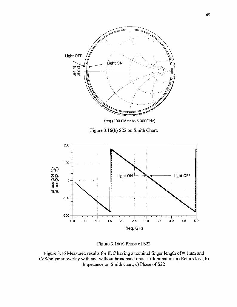
The coated IDC was then measured under the same conditions as the uncoated
IDC was measured, however, in this case, with and without illumination from the halogen
lamp. Figures 3.16(a), 3.16(b) and 3.16(c) show the measured S22 in dB, phase of S22 in
degree and S22 on the Smith Chart, respectively. (S44 denotes light ON.)
Figure 3.16(a) shows an increase in return loss when the light was on for all
frequencies. This result correlates with Figure 3.8, which also shows an increase in return
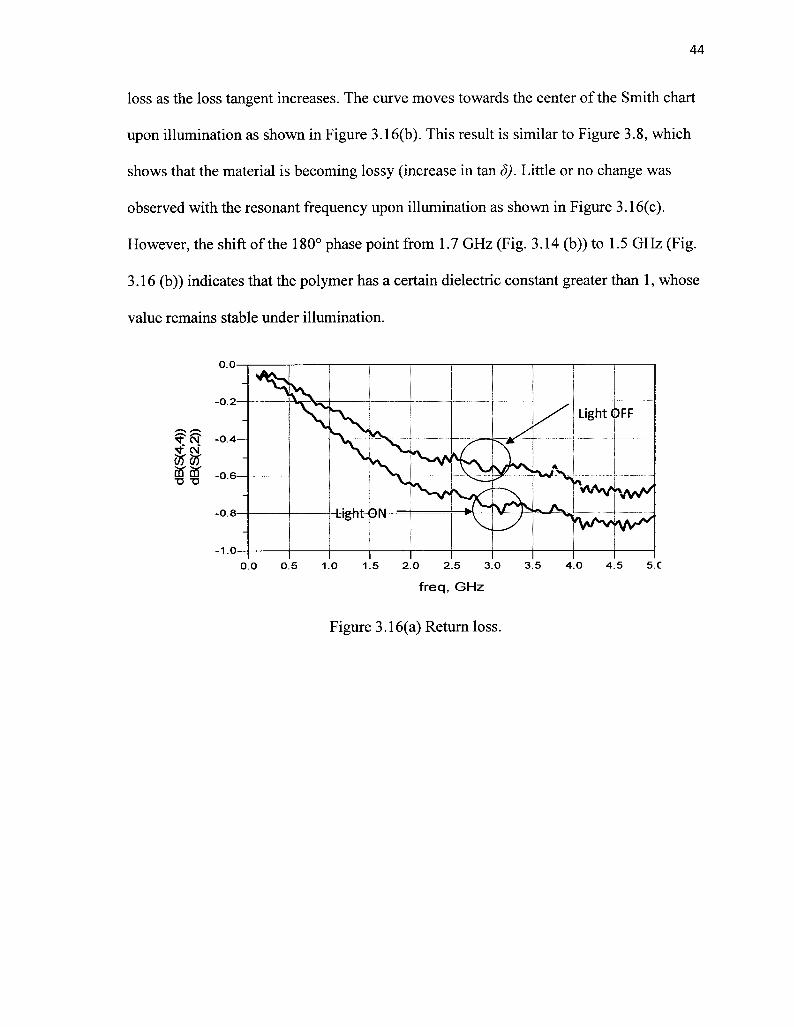
44
loss as the loss tangent increases. The curve moves towards the center of the Smith chart
upon illumination as shown in Figure 3.16(b). This result is similar to Figure 3.8, which
shows that the material is becoming lossy (increase in tan d). Little or no change was
observed with the resonant frequency upon illumination as shown in Figure 3.16(c).
However, the shift of the 180° phase point from 1.7 GHz (Fig. 3.14 (b)) to 1.5 GHz (Fig.
3.16 (b)) indicates that the polymer has a certain dielectric constant greater than 1, whose
value remains stable under illumination.
o.o
-0.2
·* CM -0.4^-" cm"OTOS-SS -0·6
-0.8
-1.0
Light OFF
vvwtvw^hght-ß?
freq, GHz
Figure 3.16(a) Return loss.
45
¿ciÌS"3iOT COCO co.C .ECLQ.
Light
200-
100-
-100-
-200-
freq (100.0MHz to 5.000GHz)
Figure 3.16(b) S22 on Smith Chart.
Light ON Light OFF
1''''1''''1''11I1111I1111I1111I0.0 0.5 1.0 1.5 2.0 2.5 3.0 3.5 4.0 4.5 5.0
freq, GHz
Figure 3.16(c) Phase of S22
Figure 3.16 Measured results for IDC having a nominal finger length of- 1mm andCdS/polymer overlay with and without broadband optical illumination, a) Return loss, b)
Impedance on Smith chart, c) Phase of S22
46
From the results shown in Figures 3.16(a), 3.16(b) and 3.16(c), it can be
concluded that the CdS/polymer mixture exhibited photoconductive properties. Relating
Figures (3.8), (3.9) (where the loss tangent was made a parameter) and Figures 3.14(a),
3.14(b) suggests there was increase in the loss tangent. An increase in loss tangent of a
material is due to polarization loss or conduction loss, and these effects can be attributed
to photo excitation as explained in Section 2.2.1. The DC resistivity of the CdS/polymer
composite under illumination was 25 ?O [34]. At this high level, it is unlikely that a
change in conductivity attributed much to a change in loss tangent.
3.6 Extraction and Modeling of Material Properties.
The extraction of the material properties and the modeling of the fabricated
structure, were done by matching the measured SIl parameters of the 1 mm finger length
IDC, with and without overlay material, to a lumped element equivalent model based on
(a) approximate IDC element values and (b) HFSS-simulated IDC S-parameters.
Advanced Design System (ADS), a commercially available microwave CAD software,
was used in the process. Figure 3.17 shows the resulting equivalent model for the all-
lumped approach (a). It comprises the SMA connector model, CPW line model, and IDC
lumped element model. The SMA is modeled as a parallel capacitor (C2) in series with
an inductor (L2) and resistor (R2), representing the transition from coaxial to CPW
propagation. The capacitor represents the shunt capacitance between the centre connector
and the outer conductor of SMA connector. The resistor and the inductor represent the
47
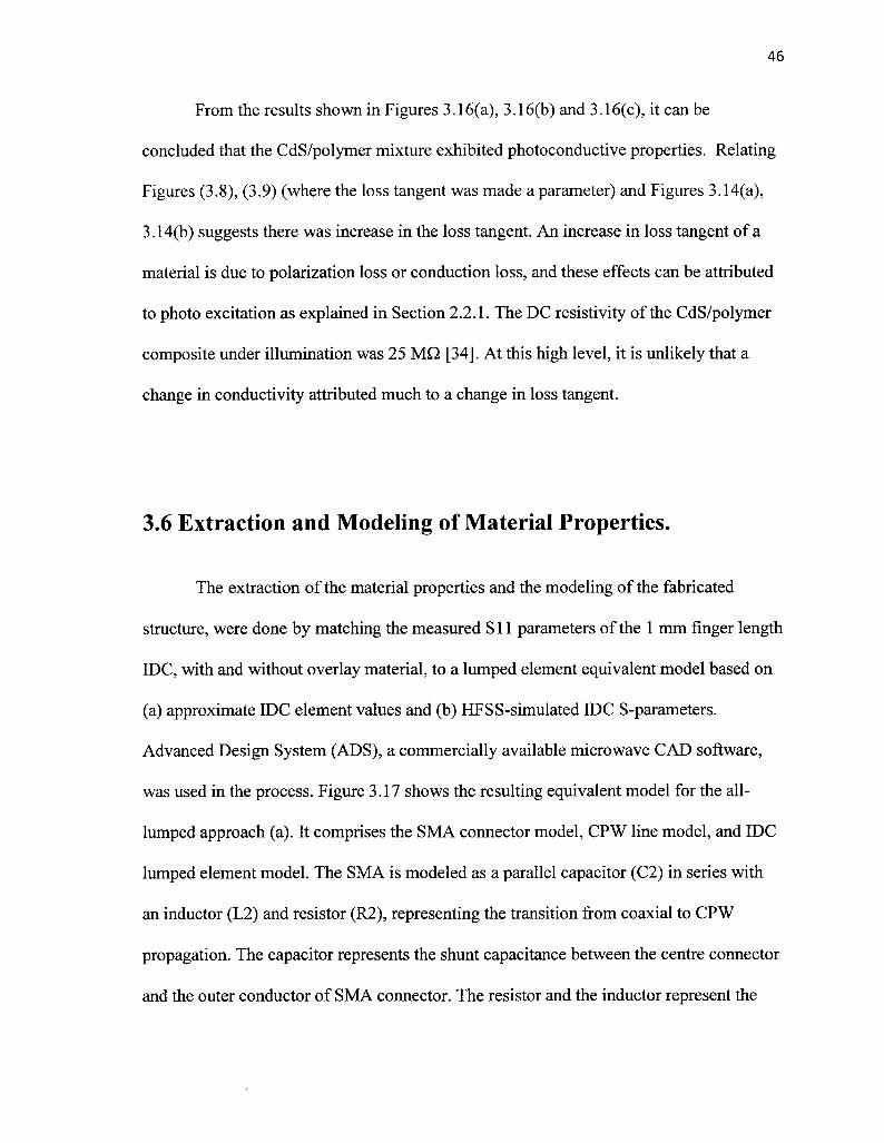
distributed resistance and the inductance of the center conductor of the connector,
respectively.
?{. _ TemiTermi
hNum=1?=50
CC2 Connector
-*-???t-RR2 CPW
CPW1W=W mmG=G mmL=L mm
LL1
RR1
IDCCC1
T-J
Figure 3.17 Lumped element equivalent circuit for the connector, CPW and IDC.
To determine the values of the elements and the parameters in the lumped
equivalent model in Figure 3.17, the CPW line model and the IDC were first modeled
and optimized to match the measured result over the range of 100 MHz to 500 MHz. It is
assumed that the connector model has little or no effect at these lower frequencies. The
geometry of the CPW line was measured with a micrometer associated with the
microscope. The measured values were gap (G) = 0.38mm, signal conductor width (S) =
1.9 mm and length L= 13.2 mm, and these values were used in the CPW model provided
by ADS. The estimated values for Cl, Rl, and Ll were determined from an approximate
model in [26] and [28] using the true (fabricated) dimensions of the IDC. ADS was then
used to tune Rl, Cl, and Ll to match the measured result over the range of 100 MHz to
500 MHz. The optimized values for the IDC model are, Cl = 1.05 pF, Ll = 1 .2 nH, Rl =
1.7 O, self-resonating approximately at 4.48 GHz. The connector model was then
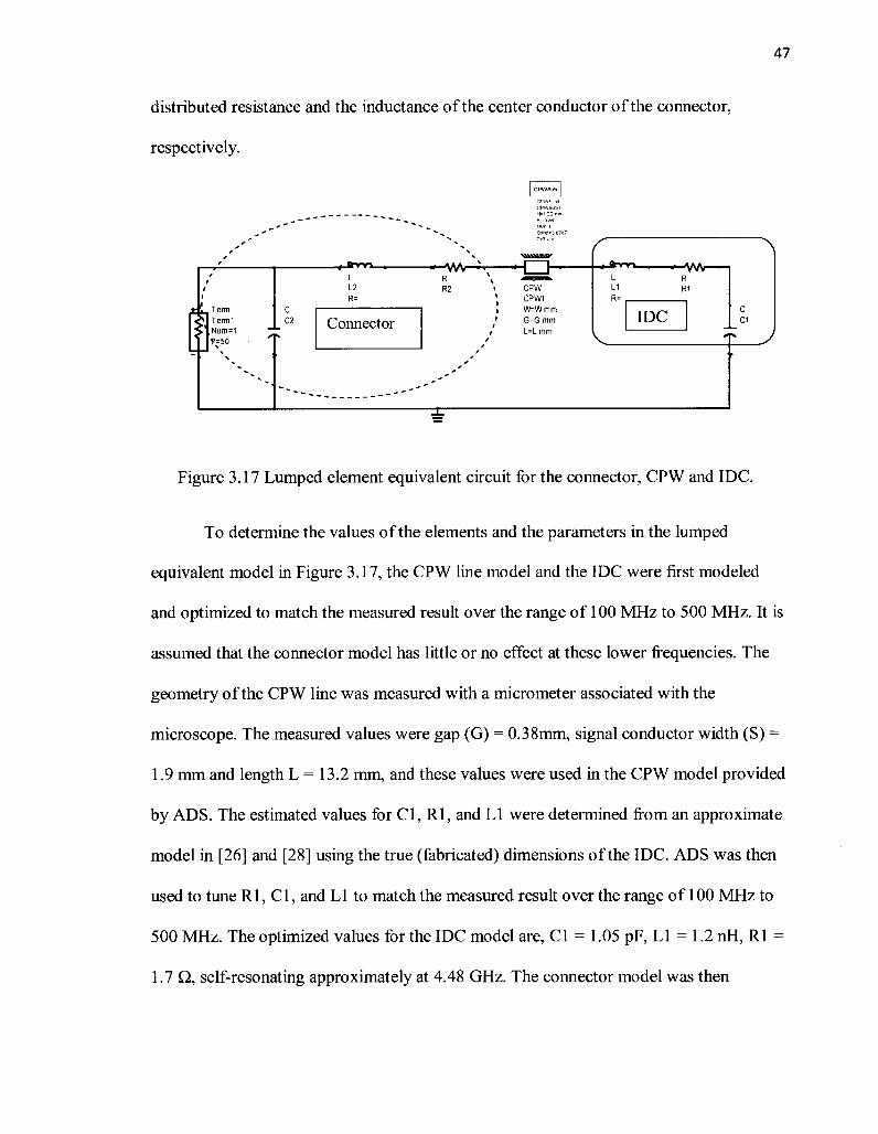
48
included and its parameters C2, L2 and R2 was varied and optimized to match the
measured result over the wider frequency range of 100 MHz to 5 GHz.
MUT
Figure 3.18 HFSS simulation structure for the fabricated IDC with MUT overlaid on theIDC
The optimized values for the connector model are L2 = 0.8 nH, C2 = 0.3 pF, R2 = 0.12 O
resonating at approximately at 1 OGHz.
Next, an HFSS simulation was performed as illustrated in Figure 3.18 to model
the CPW line and IDC. The resulting equivalent model for the hybrid lumped/HFSS
approach (b) is shown in Figure 3.19. The IDC dimensions of the fabricated structure, as
shown in Figure 3.12 and the dimensions of the CPW line were used in the HFSS model.
To account for the connector model, the S-parameters obtained from the simulation were
exported to ADS and connected to the complete model as shown in Figure 3.19.
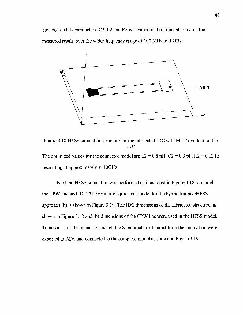
49
Termi
HFSS SP dataNum=1 ConnectorZ=SO
Figure 3.19 Equivalent lumped/HFSS model with s-parameter (SP) data from HFSS.
The two models were simulated in Agilent ADS. Figures 3.20 and 3.21 show the
correlation between the measured results, the equivalent lumped element model of the
structure and the lumped/HFSS model for the IDC with no overlay of MUT. There was a
very close agreement between the equivalent lumped element model and the
lumped/HFSS model, within 0.1 dB in magnitude of Sl 1 over 100 MHz to 5 GHz and
within 20 degrees in phase of Sl 1 up to 2.5 GHz. The HFSS model shows a better
agreement with the measured phase up to 5 GHz than the lumped model.
50
0.0
CO CN t-CO CNÍ t-"
iÏÏincù???
Lumped ModelMeasuredLumped/HFSS
freq, GHz
Figure 3.20 Return loss comparison of the measured result, lumped element equivalentmodel and lumped/HFSS model without polymer overlay.
200
100—CO CN T-
WWWVaT ^v(? (? COCO Co CO^ ^ ^a a. a -100
-200
LumpedMeasuredLumped/
Model
freq, GHz
Figure 3.21 Reflection phase comparison of the measured result, lumped elementequivalent model and lumped/HFSS model without polymer overlay.
51
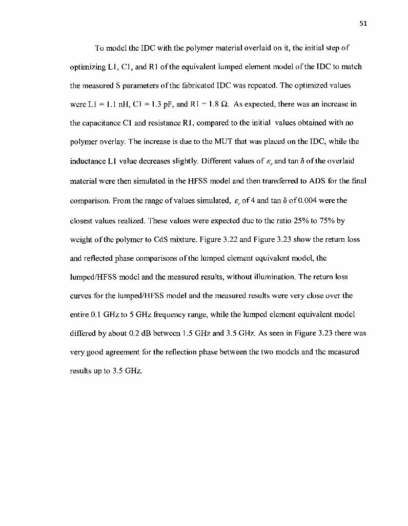
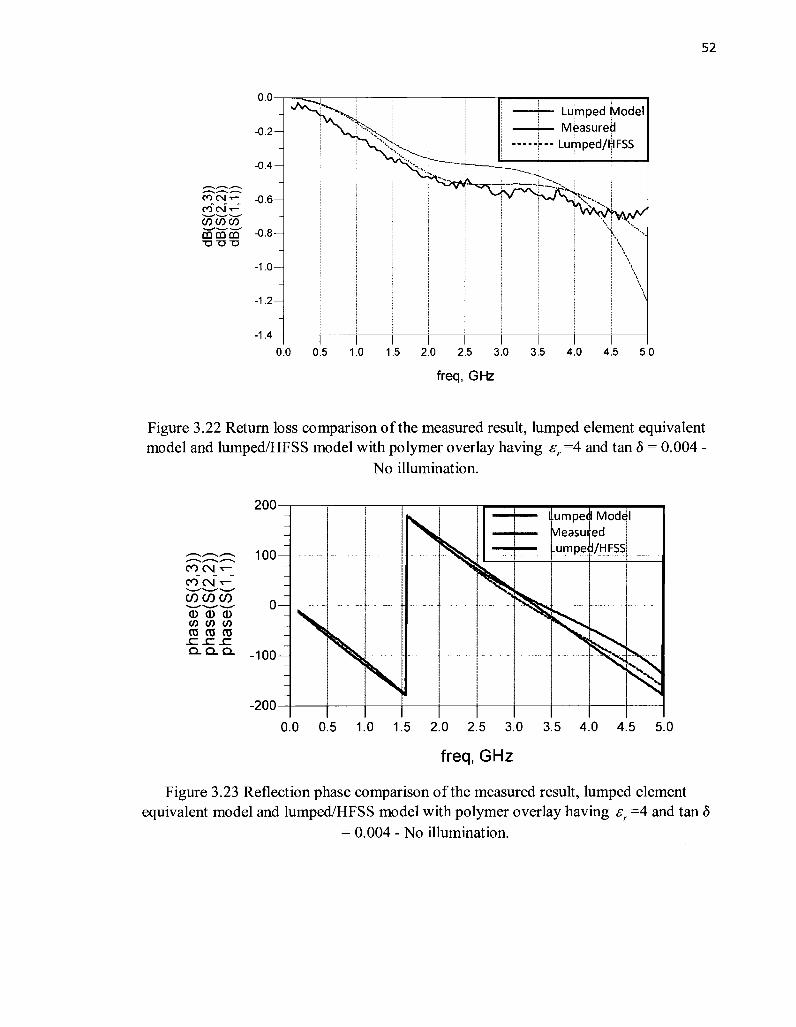
To model the IDC with the polymer material overlaid on it, the initial step of
optimizing Ll, Cl, and Rl of the equivalent lumped element model of the IDC to match
the measured S parameters of the fabricated IDC was repeated. The optimized values
were Ll = 1.1 nH, Cl = 1.3 pF, and Rl = 1.8 O. As expected, there was an increase in
the capacitance Cl and resistance Rl, compared to the initial values obtained with no
polymer overlay. The increase is due to the MUT that was placed on the IDC, while the
inductance Ll value decreases slightly. Different values of sr and tan d of the overlaid
material were then simulated in the HFSS model and then transferred to ADS for the final
comparison. From the range ofvalues simulated, sr of 4 and tan d of 0.004 were the
closest values realized. These values were expected due to the ratio 25% to 75% by
weight of the polymer to CdS mixture. Figure 3.22 and Figure 3.23 show the return loss
and reflected phase comparisons of the lumped element equivalent model, the
lumped/HFSS model and the measured results, without illumination. The return loss
curves for the lumped/HFSS model and the measured results were very close over the
entire 0. 1 GHz to 5 GHz frequency range, while the lumped element equivalent model
differed by about 0.2 dB between 1.5 GHz and 3.5 GHz. As seen in Figure 3.23 there was
very good agreement for the reflection phase between the two models and the measured
results up to 3.5 GHz.
52
COCMt- .geCO cní·«-"</íc/íc/^CûOû CQ -0.8UOO
Lumped ModelMeasuredLumped/tì FSS
freq, GHz
Figure 3.22 Return loss comparison of the measured result, lumped element equivalentmodel and lumped/HFSS model with polymer overlay having sr =4 and tan d = 0.004 -
No illumination.
OO CN T-
? ? ?CO (? C/5co co co
-C SZ SZQ. Q. Q.
200
100
-100
-200
lumpedMeasuredumped/HFSS
Model
0.0 0.5 1.0 1.5 2.0 2.5 3.0 3.5 4.0 4.5 5.0
freq, GHz
Figure 3.23 Reflection phase comparison of the measured result, lumped elementequivalent model and lumped/HFSS model with polymer overlay having sr =4 and tan d
= 0.004 - No illumination.
53
Modeling the IDC with polymer overlay and light applied, the Cl, Ll, and Rl
values of the lumped element model were re-tuned to match the S-parameters measured
with light on. The optimized values were Cl = 1.35 pF, Ll = 1.08 nH, and Rl = 2.6 O.
There was a slight increase in capacitance Cl for the lumped element equivalent model
with light on as compared to when it was off. The resistance Rl increased by 0.8 O for
the model with light on, showing that in fact the MUT is becoming more lossy. In the
HFSS model, the loss tangent of the overlaid material was increased periodically with a
random interval while keeping sr constant. The S parameters for each sweep were
exported to ADS for comparison with the measured result. A loss tangent of 0.1 1, which
is 30 times greater than the non-illuminated case, was the best fit as shown in Figure 3.24
and Figure 3.25. As seen in Figure 3.24, the lumped element model was offby about 0.2
dB in return loss for most of the frequency range, while there was better agreement
between the measured result and the lumped/HFSS model. Referring to Figure 3.25 there
was again very good agreement for the reflection phase between the two models and the
measured results up to 3.5 GHz.
54
Lumped Mod¿lMeasuredLumpdd/HFSS
COCM T-
m'aicoT3T3 ?3
freq, GHz
Figure 3.24 Return loss comparison of the measured result, lumped element equivalentmodel and lumped/HFSS model with polymer overlay having sr =4 and tan d = 0.004 -
With illumination.
200
100CO CNl T-
cd ??G??G(/)(/)(/)CO CO Co
Xl XZ XlQ.Q.Q.
-200
Lumped ModelMeasuredLumped/HFSS
-100H
0.0 0.5 1.0 1.5 2.0 2.5 3.0 3.5 4.0 4.5 5.0
freq, GHz
Figure 3.25 Reflection phase comparison of the measured result, lumped elementequivalent model and lumped/HFSS model with polymer overlay having sr =4 and tan d
= 0.004 - With illumination.
55
3.7 Chapter Summary and Conclusions
In this chapter, an original CPW-fed IDC structure was developed for in-situ
material characterization ofoptically-sensitive polymers at microwave frequencies.
Through a combination of lumped-element and EM-based modeling, and experimental
measurements, the initial characterization ofnovel CdS nanoparticle- loaded polymer
material has been successfully carried out. The extracted material properties and
equivalent circuit element values, valid for the 0. 1 GHz to 5 GHz range, are summarized
in Table 3.3.
Table 3.3 Results ofoptically-sensitive polymer material characterization using the IDCtest structure developed in this thesis
Cl(pF)
Rl(O)
Ll (nH)
Polymer sr
Polymer tan d
IDC
1.05
1.7
1.2
Polymer-Coated IDC Polymer-Coated IDC
- No Illumination
1.3
1.8
1.1
0.004
With Illumination
1.35
2.6
1.1
0.11

56
The new CdS-polymer 0.25:0.75 mixture was found to exhibit a moderate
photoconductive effect, as evidenced by a 30-fold increase in its loss tangent under
broadband optical illumination.
These initial results are promising for tunable microwave circuits, but further
work is needed to completely characterize the materials (for example at higher
microwave frequencies and at different optical wavelengths and power levels). Also,
more material development work is needed to fully explore the various nanoparticle-
polymer mixtures.
Chapter 4
Study of Optically Tunable Dipole Antenna
Given the availability of CdS composite polymer materials and their
photoconductive properties as described in Chapter 3, it is interesting to investigate how
they may now be applied to the realization of a practical optically-tuned antenna. This
chapter presents the preliminary design of an optically tunable dipole antenna for the 1 .9
GHz and 2.1 GHz GSM communication bands. The theoretical results obtained will be
useful for guiding future polymer material development which, ultimately, could lead to a
final working design.
4.1 Tunable Dipole Antenna
For the antenna design pursued here, the composite polymer is placed along the
segmented length of the arm of the dipole. Upon illumination, there will be an increase in
the conductivity of the material. Gaps between segments will become conductive creating
continuity in the length of the dipole and thereby increasing the physical length.
References [13] and [29] used such an increase in the physical length to tune the
bandwidth and the resonance frequency of a dipole antenna. In [13], PIN diodes are used
to tune frequency. Each arm of the antenna was segmented and PIN diodes were placed
between the segments as shown in Figure 4.1. The diodes were then turned ON and OFF
by an external bias voltage. In the ON state, both the electrical and the physical length of
57
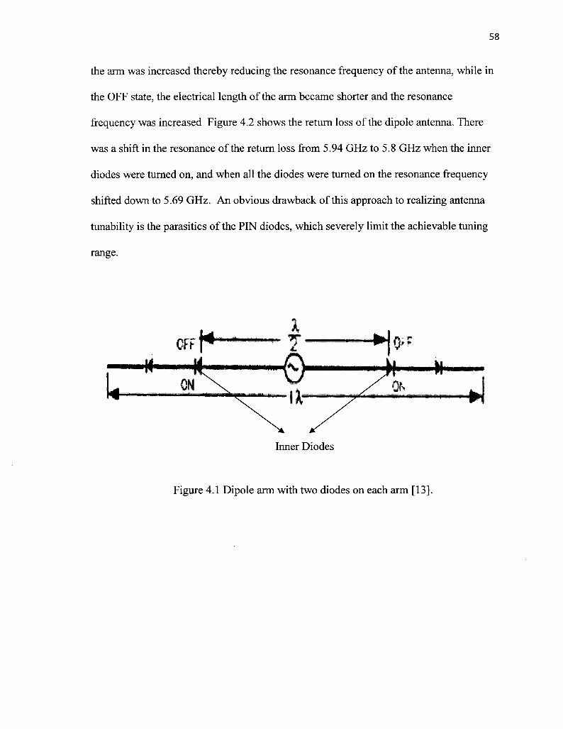
58
the arm was increased thereby reducing the resonance frequency of the antenna, while in
the OFF state, the electrical length of the arm became shorter and the resonance
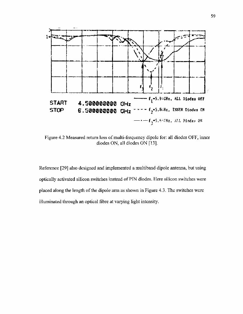
frequency was increased. Figure 4.2 shows the return loss of the dipole antenna. There
was a shift in the resonance of the return loss from 5.94 GHz to 5.8 GHz when the inner
diodes were turned on, and when all the diodes were turned on the resonance frequency
shifted down to 5.69 GHz. An obvious drawback of this approach to realizing antenna
tunability is the parasitics of the PIN diodes, which severely limit the achievable tuning
range.
l·KM
4 J\?
Inner Diodes
Figure 4.1 Dipole arm with two diodes on each arm [13].
59
— f .-5.94CHa, ALI Dioí*8 OFFstart A^mmmm ghz lSTOP 5.500000000 OHz ¦"" V3*8*' mm mùè*s m
— "^f1-5,^fHa, Ml Mudes OPs
Figure 4.2 Measured return loss of multi-frequency dipole for: all diodes OFF, innerdiodes ON, all diodes ON [13].
Reference [29] also designed and implemented a multiband dipole antenna, but using
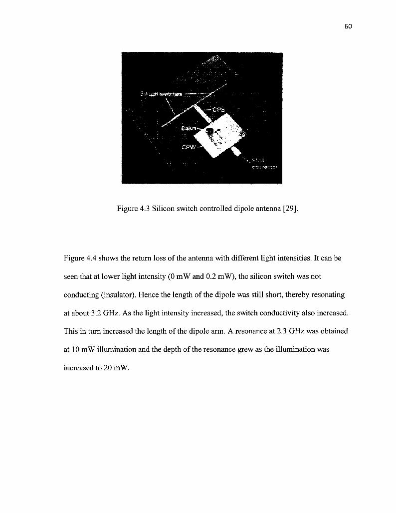
optically activated silicon switches instead of PIN diodes. Here silicon switches were
placed along the length of the dipole arm as shown in Figure 4.3. The switches were
illuminated through an optical fibre at varying light intensity.
60
m¡
B
wmmeîs^es!,I
ß
ÍKMM
*
Figure 4.3 Silicon switch controlled dipole antenna [29].
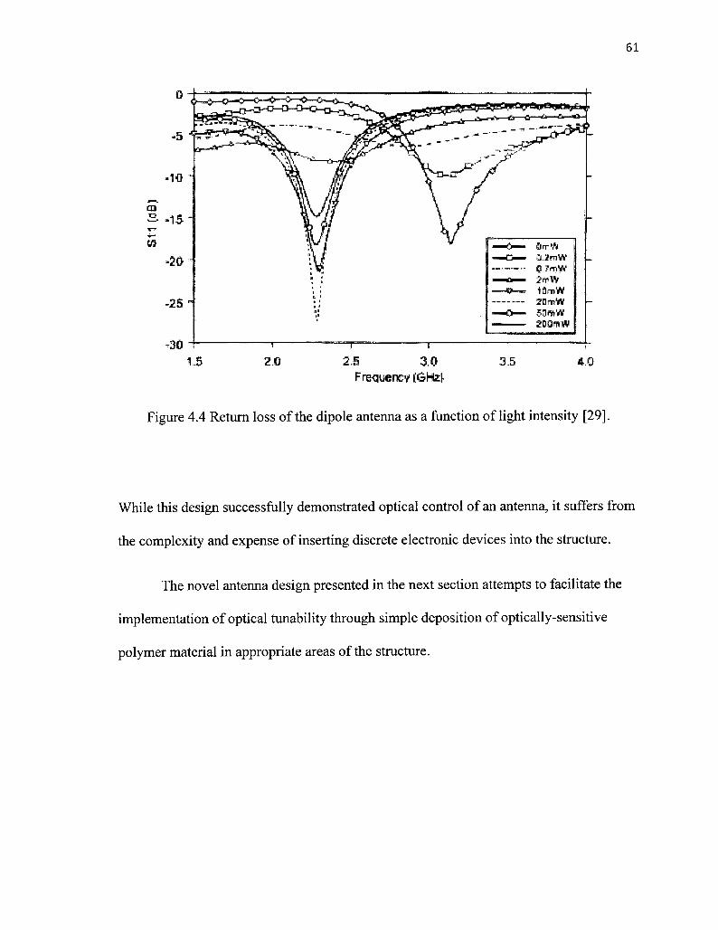
Figure 4.4 shows the return loss of the antenna with different light intensities. It can be
seen that at lower light intensity (0 mW and 0.2 mW), the silicon switch was not
conducting (insulator). Hence the length of the dipole was still short, thereby resonating
at about 3.2 GHz. As the light intensity increased, the switch conductivity also increased.
This in turn increased the length of the dipole arm. A resonance at 2.3 GHz was obtained
at 10 mW illumination and the depth of the resonance grew as the illumination was
increased to 20 mW.
61
Ott '?O.MWQJmW2*WlämWznrnW50»W20OmW
2.5 30Frequency tôHzl
Figure 4.4 Return loss of the dipole antenna as a function of light intensity [29].
While this design successfully demonstrated optical control of an antenna, it suffers from
the complexity and expense of inserting discrete electronic devices into the structure.
The novel antenna design presented in the next section attempts to facilitate the
implementation of optical tunability through simple deposition of optically-sensitive
polymer material in appropriate areas of the structure.

62
4.2 Tunable Dipole Antenna Design for GSM Band (1900 MHz
to 2100 MHz).
The goal of this section is to achieve a tunable antenna whose centre frequency
shifts from 1 .9 GHz to 2. 1 GHz upon optical illumination. Such a design is intended to
provide partial coverage of the complete 1.9 GHz to 2.2 GHz frequency band with a
reasonable impedance match (better than 10 dB return loss).
A half-wave dipole antenna can be designed using the transmission line model
[30]. The antenna will be designed on Corning 7059 glass to allow the transmittance of
light through the substrate. The length of each arm L is given as L=lef/4
with Xeff = —^= (4.1)f F
where / is the resonance frequency (1.9 GHz and 2.1 GHz) while c is the speed of light
3.0?108 ms"1. The effective dielectric constant seff can be calculated from Eqn. (4.2) [H].
er+l sr-\ 1_2 yj\ + \2d/Wt«=^+\ L .I.,,,. (4-2)
This is valid for a microstrip line, but will serve to provide an initial estimate of the
required strip length for the printed dipole without an underlying ground plane.
The parameters of the glass substrate are er = 5.84, and thickness d=T.22 mm. For a
trace width arbitrarily chosen as W = 0.85 mm, the seff - 3.94 and therefore the length L
at 1.9 GHz is 19.89 mm while at 2.1 GHz the length is 18.23 mm.
63
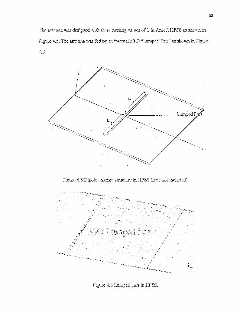
The antenna was designed with these starting values of L in Ansoft HFSS as shown in
Figure 4.5. The antenna was fed by an internal 50 O "Lumped Port" as shown in Figure
4.6.
L
L
Figure 4.5 Dipole antenna structure in HFSS (feed not included).
?¡> ì?\
h
Figure 4.6 Lumped port in HFS
64
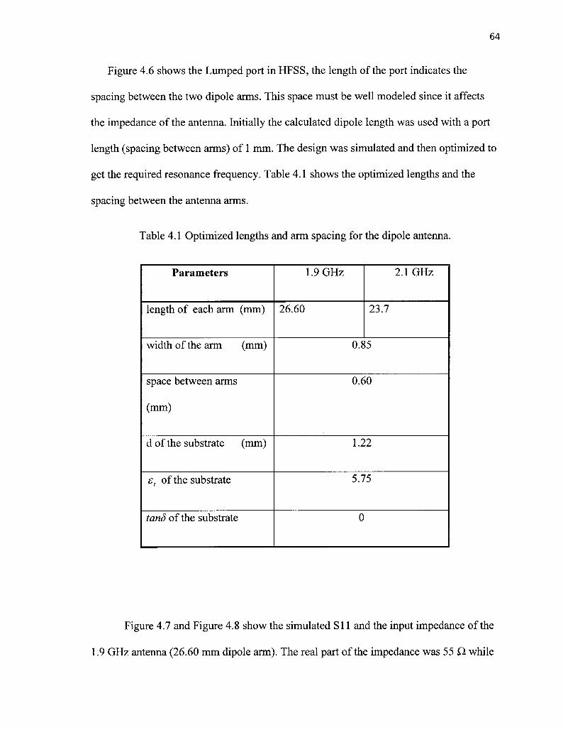
Figure 4.6 shows the Lumped port in HFSS, the length of the port indicates the
spacing between the two dipole arms. This space must be well modeled since it affects
the impedance of the antenna. Initially the calculated dipole length was used with a port
length (spacing between arms) of 1 mm. The design was simulated and then optimized to
get the required resonance frequency. Table 4.1 shows the optimized lengths and the
spacing between the antenna arms.
Table 4.1 Optimized lengths and arm spacing for the dipole antenna.
Parameters 1.9GHz 2.1 GHz
length of each arm (mm) 26.60 23.7
width of the arm (mm) 0.85
space between arms
(mm)
0.60
d of the substrate (mm) 1.22
e, of the substrate 5.75
tanô of the substrate
Figure 4.7 and Figure 4.8 show the simulated SIl and the input impedance of the
1.9 GHz antenna (26.60 mm dipole arm). The real part of the impedance was 55 O while
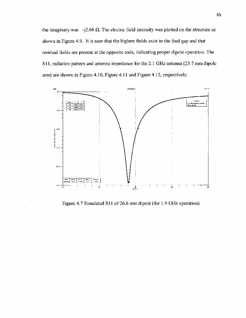
65
the imaginary was -J2.68 O. The electric field intensity was plotted on the structure as
shown in Figure 4.9. It is seen that the highest fields exist in the feed gap and that
residual fields are present at the opposite ends, indicating proper dipole operation. The
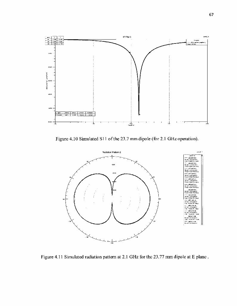
Sl 1, radiation pattern and antenna impedance for the 2.1 GHz antenna (23.7 mm dipole
arm) are shown in Figure 4.10, Figure 4.1 1 and Figure 4.12, respectively.
Figure 4.7 Simulated Sl 1 of 26.6 mm dipole (for 1.9 GHz operation).
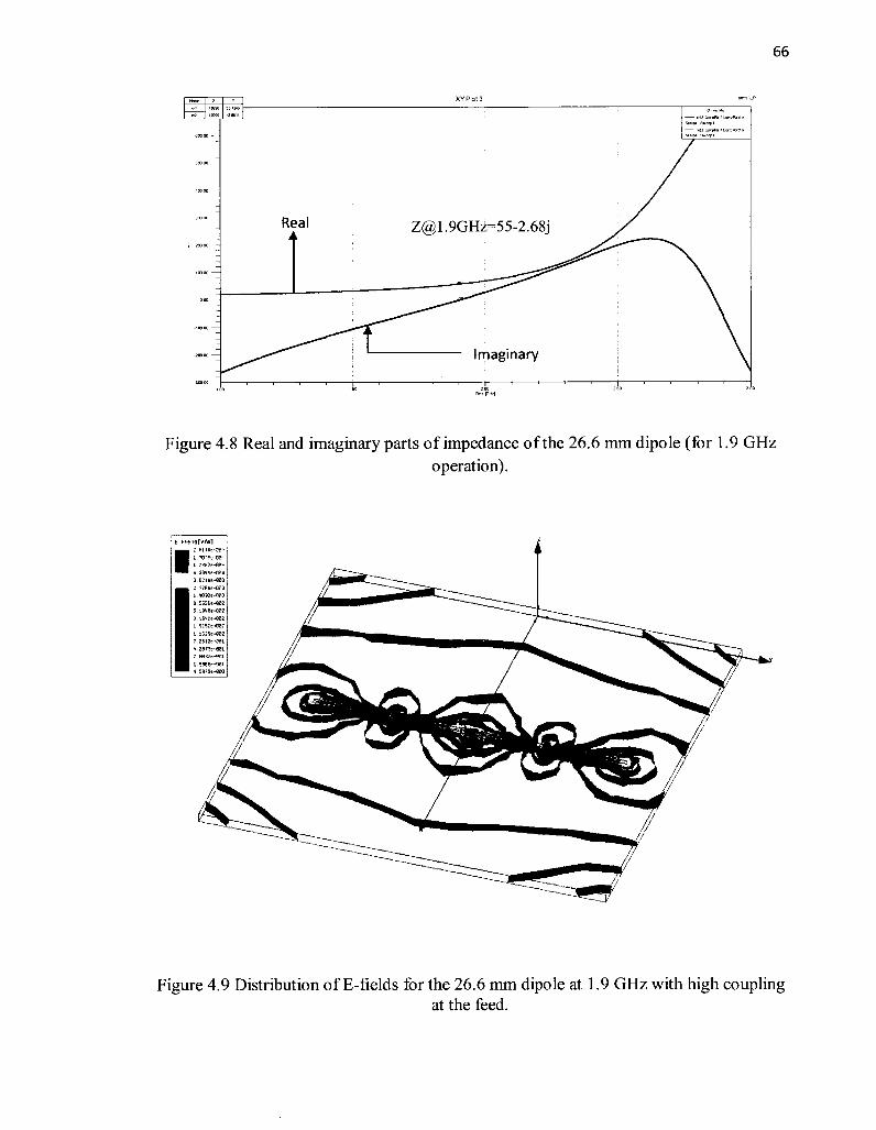
66
Real [email protected]=55-2.68j
Imaginary
Figure 4.8 Real and imaginary parts of impedance of the 26.6 mm dipoIe (for 1.9 GHzoperation).
Figure 4.9 Distribution of ?-fields for the 26.6 mm dipole at 1.9 GHz with high couplingat the feed.
67
Figure 4.10 Simulated SII of the 23.7 mm dipole (for 2.1 GHz operation).
Radiation Pattern 2
Se tup 1 LaaIAOaplKe
Figure 4.1 1 Simulated radiation pattern at 2.1 GHz for the 23.77 mm dipole at E plane .
68
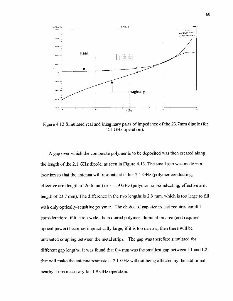
AfBDl Corrorcitfcjr. XY PbI 3
------ in«LuiTpft«!1.ümDR.MÍIStupì Swnpl
Sc6ibi 'Sweepi
Real
¦ÏOO Imaginary
JOO
Figure 4.12 Simulated real and imaginary parts of impedance of the 23.7mm dipole (for2.1 GHz operation).
A gap over which the composite polymer is to be deposited was then created along
the length of the 2.1 GHz dipole, as seen in Figure 4.13. The small gap was made in a
location so that the antenna will resonate at either 2.1 GHz (polymer conducting,
effective arm length of 26.6 mm) or at 1.9 GHz (polymer non-conducting, effective arm
length of 23.7 mm). The difference in the two lengths is 2.9 mm, which is too large to fill
with only optically-sensitive polymer. The choice of gap size in fact requires careful
consideration: if it is too wide, the required polymer illumination area (and required
optical power) becomes unpractically large; if it is too narrow, then there will be
unwanted coupling between the metal strips. The gap was therefore simulated for
different gap lengths. It was found that 0.4 mm was the smallest gap between Ll and L2
that will make the antenna resonate at 2. 1 GHz without being affected by the additional
nearby strips necessary for 1 .9 GHz operation.
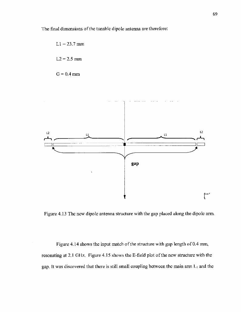
69
The final dimensions of the tunable dipole antenna are therefore:
Ll = 23.7 mm
L2 = 2.5 mm
G = 0.4 mm
L2Ll
IC
LlL2
gap
r
Figure 4.13 The new dipole antenna structure with the gap placed along the dipole arm.
Figure 4.14 shows the input match of the structure with gap length of 0.4 mm,
resonating at 2.1 GHz. Figure 4.15 shows the ?-field plot of the new structure with the
gap. It was discovered that there is still small coupling between the main arm Li and the
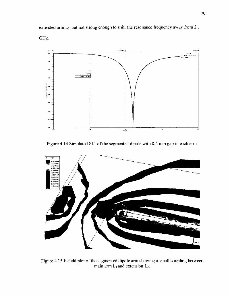
70
extended arm L2, but not strong enough to shift the resonance frequency away from 2. 1
GHz.
XY Plot 2
Figure 4.14 Simulated SIl of the segmented dipo Ie with 0.4 mm gap in each arm.
E fieldU/iil
Figure 4.15 ?-field plot of the segmented dipo Ie arm showing a small coupling betweenmain arm Li and extension L2.
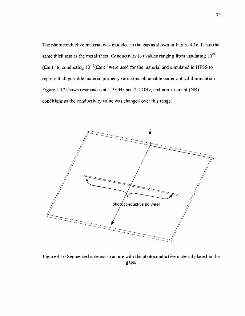
71
The photoconductive material was modeled in the gap as shown in Figure 4.16. It has the
same thickness as the metal sheet. Conductivity (s) values ranging from insulating 10"
(Qm)"1 to conducting 1O+ '(Qm)'' were used for the material and simulated in HFSS torepresent all possible material property variations obtainable under optical illumination.
Figure 4.17 shows resonances at 1.9 GHz and 2.1 GHz, and non-resonant (NR)
conditions as the conductivity value was changed over this range.
á
/
Figure 4.16 Segmented antenna structure with the photoconductive material placed in thegaps.
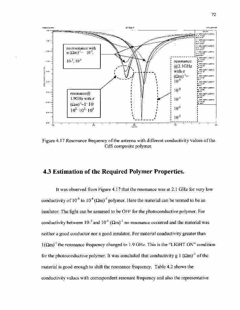
72
no resonance with
s (O??)
10- , 10 ' resonance
@2.1GHzwith s(Op?) =
resonance
1.9GHz with s
(O???'=1· 10'IO2' IO3' IO4
------- dBS<UinpRirt1.Lim«>r11))Sitie' : SwaaplScorcile -OO G
dBS( L urpRj rt 1 . L unfbrl 1 ) )
|- dB(S(LiiTpR)rt1.LiiTTftitl))fpi j Sweep ?.1Id=OOOf
(- dB(S(Lu>TpR)rtl.Lun^ftjrtl))
dB(S( L uieFb ril . LiiiBftrl 1 ) )
dB(S(t. UTfjR) iti .Lurnrtirl 1 ) )
*- dB(S(LixiipRiftUiiri(A>ri1))InI=1IO'I- dB(S(LiJTfiRjrii,Liii«ftjr11))
h dB(S(t.im)Riri1,Lunftirl1))
I dB(S{Lii7pR>rtUnirli»
Figure 4.17 Resonance frequency of the antenna with different conductivity values of theCdS composite polymer.
4.3 Estimation of the Required Polymer Properties.
It was observed from Figure 4.17 that the resonance was at 2.1 GHz for very low
conductivity of 10"9 to 1 O^ (Qm)"1 polymer. Here the material can be termed to be aninsulator. The light can be assumed to be OFF for the photoconductive polymer. For
conductivity between 10-3 and 10"1 (Qm)"1 no resonance occurred and the material wasneither a good conductor nor a good insulator. For material conductivity greater than
1(Qm)"1 the resonance frequency changed to 1.9 GHz. This is the "LIGHT ON" condition
for the photoconductive polymer. It was concluded that conductivity g 1 (Qm)" of the
material is good enough to shift the resonance frequency. Table 4.2 shows the
conductivity values with correspondent resonant frequency and also the representative

73
material type.
The future generations of optically sensitive polymers will require conductivities¦j ¡yvarying from 1 0 S/m or lower (sufficiently insulating with light OFF) to 1 0 S/m or
higher (sufficiently conducting with light ON) to be useful in this application.
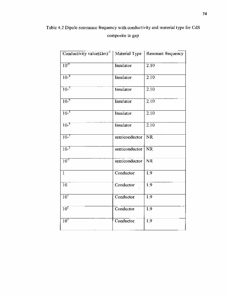
74
Table 4.2 Dipole resonance frequency with conductivity and material type for CdScomposite in gap
Conductivity value(Qm)" Material Type Resonant frequency
10" Insulator 2.10
10- Insulator 2.10
10-' Insulator 2.10
10-° Insulator 2.10
10-3 Insulator 2.10
10-H Insulator 2.10
10-J semiconductor NR
10- semiconductor NR
10" semiconductor NR
Conductor 1.9
10 Conductor 1.9
10' Conductor 1.9
10z Conductor 1.9
10J Conductor 1.9
4.4 Conclusion
75
This chapter presented the preliminary design of an optically tunable dipole
antenna for the 1.9 GHz and 2.1 GHz GSM communication bands. A printed dipole
having 23.7 mm arm length and 0.4 mm gaps filled with photoconducting material,
would produce the desired performance. The theoretical results obtained indicate that
future polymer material development should aim to achieve conductivities varying from
10"3 S/m or lower (sufficiently insulating with light OFF) to 1O+2 S/m or higher(sufficiently conducting with light ON) in order to be useful in this application.
Chapter 5
Conclusion and Future Work
5.1 Conclusion
The characterization and extraction of material properties of polymer containing
CdS nanoparticles was done in this thesis. The reflection method was used for the
material characterization of planar microwave interdigitated capacitors overlaid with the
mixture of polymer containing CdS nanoparticles with 75% to 25% ratio by weight. The
measured return loss and the S 1 1 on the Smith chart as a function of optical illumination
shows that the material was photoconductive. There was an increase in return loss when
the light was on for all frequencies and the curve of Sl 1 also moved toward the center of
the Smith chart. This was due to polarization loss or conduction loss exhibited by the
material under test. For the extraction of material properties, dielectric constant of 4 and
loss tangent of 0.004 was obtained with light off, however the dielectric constant remains
unchanged for light on while the loss tangent increased to 0.1 1. The extraction of the
material properties was done by matching the Sl 1 parameters of the fabricated model,
lumped element equivalent model and the HFSS fabricated model for each state using
commercial avallabile software Agilent ADS.
The photoconductive properties of the material were used in the theoretical design
of a tunable a dipole antenna for 1900MHz and 2100MHz band. The tunable dipole
antenna was designed in ANSOFT HFSS a, 3D full-wave electromagnetic field
76
77
simulator. It was concluded that conductivity near 1 (Qm)"1 of the material is enough toshift the resonance frequency from 2100MHZ to 1900MHz if the photoconductive
material was placed along the segmented gap of the antenna arm structure .
5.2 Future Work.
An interdigitated capacitor with smaller feature size would have given a better
response, but due to the feature size of the David Mann pattern generator, the initial
??µp? spacing between the fingers was increased to 12.5µ??. Also another method of
etching would have been preferred. The wet etching method led to further increase in the
minimum size feature of the interdigitated capacitor. The test structure also should have
been de-embedded to extract the actual capacitance of the IDC. Conductivity
measurements of the polymer using the four point probe method should be done in order
to determine the actual conductivity as a function of light intensity. The theoretical design
tunable antenna should be fabricated and tested to confirm it predicted performance in
switching from 1900MHz to 2100MHz operation.
78
REFERENCES
[I] B. Boyer, J. Haidar, A. Vilcot, and M. Bouthinon, "Tunable microwave load based on basedPhotoinduced plasma in silicon" IEEE Transaction on Microwave Theory and Techniques,vol.45, issue 8, pp. 1362-1367, Aug. 1997.
[2] R.K. Shevgaonkar and S. Shevgaonkar, "Study of optically controlled microwave devices"International Union ofRadio Science: XXLK General Assembly, August 7-16, 2008, Chicago,USA. [online]. Available: http://www.ursi.org/Proceedings/ProcGA05/pdf/D07b.5(0 1 8 1 7).pdf[Accessed: May. 17, 2009]
[3] M.R. Chaharmir, J. Shaker, M. Cuhaci and A. Sebak, "Novel Photonically-controlledreflectarray antenna" IEEE Transactions on Antennas and Propagation, vol. 54, no. 4, pp1134-1 142, April 2006.
[4] R.E. Hummel "Electrical properties of materials" in Understanding Materials Science, 2ned., New York: Springer, 2005, pp. 186-2 10.
[5] D. Seanor, Electrical Properties ofPolymers, New York and London: Academic Pr, Nov.1982, pp. 116-122.
[6] Y. Wang "Photoconductivity of fullerene" Central research and Development, Du Pont Co ,Nature 356, pp 585-587, April 1992.
[7] Y. Chen, et. al, "Researches on the photoconductivity and UV-visible absorption spectra ofthe first Coo- chemically modifies poly (N-vinlycarbazole,) " Polymer bulletin, vol. 36, no. 2,pp 203- 208, Feb. 1996.
[8] J. E. Mark, Ed., Physicalproperties ofpolymer handbook, 2nd ed., New York: Springer,2007, pp. 11-14,38-40.
[9] A.A. Zaky and R. Hawley, Dielectric Solids, London: Dover, 1970, pp 7-22.
[10] L.F. Chen et al., Microwave Electronics: Measurement and Materials Characterization,NY: Chichester, Wiley 2004. pp. 11-14, 38-40
[II] D.M. Pozar, Microwave Engineering, 3rd ed., New York: Wiley, 2005.pp.9-l 1, 160-165.[12] T. Blythe and D. Bloor, Electrical Properties ofPolymers, 2n Ed. New York: Cambridge
University press 2005, pp 38 -57.
[13] A. Petosa, D.J. Roscoe, S. Ittipitiboon and M. Cuhaci "Tunable Dipole Antennas", IEEEAntenna and Propagation, vol. 2, no.5 July 1993. pp 672-675.
[14] A.R. Brown, and G.M. Rebeiz, "A varactor-tuned RF filter" IEEE Transaction on
79
Microwave Theory and Techniques, vol. 48, issue 7, pp. 1 157 - 1 160, Jul. 2000.
[15] Y. Fukuda, Y. Otani, H. Toyota, and T. Ono, 'Electrical Characterization Techniques ofThin Film Using Metal-Insulator-Metar Japanese Journal ofapplied Physics, vol. 46, pp.6984-6986, 2007.
[16] J.A. Chilton and M.T. Goosey, Special polymersfor electronics & optoelectronics,Chapman & Hall, London, 1995, pp 23-27, 284-305.
[17] S. Nespurek, V. Cimrova and J. Pfleger, "Charge carrier photogeneration in polymers"Colloid & Polymer Science, vol. 269, no. 6, pp 556-565, 1991.
[18] T.K. Daubler, I. Glowacki, U. Scherf, J. Ulanski, H.H. Horhold and D. Neher"Photogeneration and transport of charge carriers in hybrid materials of conjugated polymersand dye-sensitive T1O2" Journal ofPhysics, vol. 86, no. 12, 1999.
[19] S. Tay, et al., "Photorefractive polymer composite operating at the optical communicationwavelength of 1550nm" Appliedphysics letters, vol. 85, no. 20, pp 4561- 4563, 2004
[20] B. Kippelen and N. Peyghambarian, "Photorefractive polymers and their application,"polymersfor photonics applications II, vol. 161, 2003, pp 87-156.
[2I]Y. Yashchyn, and J. Modeski, "Low-cost ferroelectric-ceramic polymer scan antenna," inProceedings ofSBMO/IEEE MTT-S International Conference, 2003, vol.1, pp40 1-405.
[22] J.H. Schaffner, et al., "Microwave Components with MEMS Switches" 3(fh EuropeanMicrowave Conference, 2000.
[23] S. Gevorgian, A. Vorobiev, D. Kuylenstierna, A. Deleniv, S. Abadei, A. Eriks- son, and P.Rundqvist, "Silicon substrate integrated tunable ferroelectric devices for microwavecomponents," Integrated Ferroelectrics, 2004, vol. 66, issue 1, pp. 125-138.
[24] B. Acikel, "High Performance Barium Strontium Titanate Varactor Technology for LowCost Circuit Applications," Ph.D. dissertation, University of California, Santa Barbara,USA, 2002.
[25] B. Pratsuik, Y. Prokopenko, and Y. Poplayko, "Tunable sphere and cubic dielectricresonator" Microwave, Radar and Wireless Communications, 2008 ,pp 1-4.
80
[26] I.D. Robertson and S. Lucyszyn, RFIC and MMIC Design and Technology, 2" ed., London:Institution of Electrical Engineers, 2001.
[27] Y. Fukuda, Y. Otani, H. Toyota and T. Ono, "Electrical Characterization Techniques ofdielectric thin films using metal-insulator-metal structures," Japanese Journal ofAppliesPhysics, vol. 46, no. 10b, pp 6984-6986, Oct. 2007.
[28] R. Esfandiari, D.W. Maki, and M. Siracusa, "Design of Interdigitated Capacitors and TheirApplication to Gallium Arsenide," IEEE Transaction on Microwave Theory and Techniques,vol. 31, issue 1, pp 57-64, Jan. 1983.
[29] C. J. Panagamuwa, A. Chauraya and J. C. Vardaxoglou, "Frequency and beamreconfigurable antenna using photoconduction switches", IEEE Transactions on Antennasand Propagation, vol. 54, no. 2, pp. 449-454, February 2006.
[30] N. Tavassolian, G.E. Ponchak, and J. Papapolymerou, "Compact conformai dipole antennaon organic substrate for 2.4 GHz applications" Antennas and Propagation SocietyInternational Symposium, July 2008.
[31] Corning 7059 Barium Borosilicate properties:http://www.vinkarola.com/pdf/CorningGlass 7059 Properties.pdf, 2003 [Sept, 8 2008].
[32] R. Venkatesha and P. Przemyslaw, "Cognitive Functionality in Next Generation WirelessNetworks: Standardization Efforts" IEEE Communications Magazine, pp. 72-78, April 2008.
[33] Bruce E. Carey et.al "Flexible Frequency Discrimination Subsystems for ReconfigurableRadio Front Ends" EURASIP Journal on wireless communications and Networking , vol.5pp. 354-363 March 2005.
[34] Private Communication, S. McGarry, Department of Electronics, Carleton University,Ottawa Ontario.
[35] LM. Campbell, Introduction to Synthetic Polymers, Oxford Science Publications, 196,1994.