Embed Size (px)
Citation preview
Characterization of Electrostatic Potential and Trapped Charge in
Semiconductor Nanostructures using Off-Axis Electron Holography
by
Zhaofeng Gan
A Dissertation Presented in Partial Fulfillment of the Requirements for the Degree
Doctor of Philosophy
Approved April 2015 by the Graduate Supervisory Committee:
Martha R. McCartney, Co-Chair
David J. Smith, Co-Chair Jeffery Drucker Peter A. Bennett
ARIZONA STATE UNIVERSITY
May 2015
ABSTRACT
Off-axis electron holography (EH) has been used to characterize electrostatic
potential, active dopant concentrations and charge distribution in semiconductor
nanostructures, including ZnO nanowires (NWs) and thin films, ZnTe thin films, Si NWs
with axial p-n junctions, Si-Ge axial heterojunction NWs, and Ge/LixGe core/shell NW.
The mean inner potential (MIP) and inelastic mean free path (IMFP) of ZnO NWs
have been measured to be 15.3V±0.2V and 55±3nm, respectively, for 200keV electrons.
These values were then used to characterize the thickness of a ZnO nano-sheet and gave
consistent values. The MIP and IMFP for ZnTe thin films were measured to be 13.7±0.6V
and 46±2nm, respectively, for 200keV electrons. A thin film expected to have a p-n
junction was studied, but no signal due to the junction was observed. The importance of
dynamical effects was systematically studied using Bloch wave simulations.
The built-in potentials in Si NWs across the doped p-n junction and the Schottky
junction due to Au catalyst were measured to be 1.0±0.3V and 0.5±0.3V, respectively.
Simulations indicated that the dopant concentrations were ~1019cm-3 for donors and ~1017
cm-3 for acceptors. The effects of positively charged Au catalyst, a possible n+-n--p junction
transition region and possible surface charge, were also systematically studied using
simulations.
Si-Ge heterojunction NWs were studied. Dopant concentrations were extracted by
atom probe tomography. The built-in potential offset was measured to be 0.4±0.2V, with
the Ge side lower. Comparisons with simulations indicated that Ga present in the Si region
was only partially activated. In situ EH biasing experiments combined with simulations
i
indicated the B dopant in Ge was mostly activated but not the P dopant in Si. I-V
characteristic curves were measured and explained using simulations.
The Ge/LixGe core/shell structure was studied during lithiation. The MIP for LixGe
decreased with time due to increased Li content. A model was proposed to explain the
lower measured Ge potential, and the trapped electron density in Ge core was calculated to
be 3×10¹⁸ electrons/cm3. The Li amount during lithiation was also calculated using MIP
and volume ratio, indicating that it was lower than the fully lithiated phase.
ii

DEDICATION
To my parents
iii
ACKNOWLEDGMENTS
First of all, I would like to express my deepest gratitude to my supervisors,
Professor Martha R. McCartney and Regents’ Professor David J. Smith, for their support,
guidance and encouragement that made everything I achieved possible during my PhD
study. Their enthusiasm, meticulous attitudes, precise insight and great patience in doing
research and teaching students have deeply impressed me and educated me as good
characteristics for my future career.
I would like to thank Professors Jeff Drucker and Peter Bennett for helpful
suggestions and for serving on my dissertation committee. I am grateful for the use of
facilities in the John M. Cowley Center for High Resolution Electron Microscopy. Special
thanks to Karl Weiss, Dr. Zhenquan Liu and Dr. Toshihiro Aoki for their technical support
and assistance throughout my research. The financial support from US Department of
Energy (Grand No. DE-FG02-04ER46168) is gratefully acknowledged.
I also would like to express my deep appreciation to Dr. S. Tom Picraux, Dr.
Jinkyoung Yoo of Los Alamos National Lab, Dr. Daniel E. Perea, Dr. Chongmin Wang of
Pacific Northwest National Lab, and Professor Hongbin Yu, Yonghang Zhang of Arizona
State University for their collaboration and for providing the samples characterized in this
dissertation.
Particular thanks to our research group members- Dr. Lin Zhou, Dr. Kai He, Dr.
Luying Li, Dr. Wenfeng Zhao, Dr. Lu Ouyang, Dr. Jaejin Kim, Dr. Michael Johnson, Dr.
Dinghao Tang, Dr. Sahar Farjami, Sahar Hihath, Allison Boley, Ajit Dhamdhere, Jing Lu,
Sirong Lu, Thomas McConkie, Xiaomeng Shen, Brian Tracy, Majid Vaghayenegar,
HsinWei Wu, Desai Zhang, and et al, for their friendship and support.
iv

Last but not least, I am most grateful to my family for their love and support.
v
TABLE OF CONTENTS
Page
LIST OF TABLES .................................................................................................................. ix
LIST OF FIGURES ................................................................................................................. x
CHAPTER
1 INTRODUCTION ....................................................................................................... 1
1.1 Background ............................................................................................................ 1
1.2 Charge Distribution and Band Alignment in Semiconductors ............................ 5
1.2.1 p-n Junction .................................................................................................. 5
1.2.2 Metal Semiconductor Contact ..................................................................... 9
1.2.3 Heterojunction ............................................................................................ 13
1.3 Growth of Semiconductor Nanostructures ......................................................... 16
1.3.1 Epitaxial Growth Techniques .................................................................... 16
1.3.2 Nanowire Growth ....................................................................................... 17
1.4 Outline of Dissertation ........................................................................................ 19
References .................................................................................................................. 22
2 EXPERIMENTAL DETAILS ................................................................................... 25
2.1 Off-Axis Electron Holography ........................................................................... 25
2.1.1 Introduction ................................................................................................ 25
2.1.2 Theory and Hologram Reconstruction ...................................................... 26
2.1.3 Mean Inner Potential .................................................................................. 33
2.1.4 Experimental Setup .................................................................................... 35
2.2 Scanning Transmission Electron Microscopy .................................................... 39
vi

CHAPTER Page
2.3 Electron-Energy-Loss Spectroscopy ................................................................... 41
2.4 Sample Preparation .............................................................................................. 42
References .................................................................................................................. 45
3 MEAN INNER POTENTIAL AND INELASTIC MEAN FREE PATH OF ZnO
AND ZnTe ................................................................................................................. 47
3.1 MIP and IMFP of ZnO NWs .............................................................................. 47
3.1.1 Introduction ................................................................................................ 47
3.1.2 Experimental Details and Results .............................................................. 49
3.1.3 Conclusions ................................................................................................ 56
3.2 MIP and IMFP measurement of ZnTe ................................................................ 57
3.2.1 Introduction ................................................................................................ 57
3.2.2 Experimental Details and Results .............................................................. 58
3.2.3 Simulation of Dynamical Effects .............................................................. 65
3.2.4 Conclusions ................................................................................................ 69
References .................................................................................................................. 71
4 MAPPING ELECTROSTATIC PROFILES ACROSS AXIAL p-n JUNCTIONS
IN Si NANOWIRES USING OFF-AXIS ELECTRON HOLOGRAPHY ............ 74
4.1 Introduction ......................................................................................................... 74
4.2 Experimental Details ........................................................................................... 76
4.3 Results and Discussions ...................................................................................... 78
4.4 Conclusions ......................................................................................................... 88
References .................................................................................................................. 89
vii
CHAPTER Page
5 MEASUREMENT OF ACTIVE DOPANTS IN AXIAL Si-Ge NANOWIRE
HETEROJUNCTIONS USING OFF-AXIS ELECTRON HOLOGRAPHY AND
ATOM-PROBE TOMOGRAPHY ........................................................................... 91
5.1 Introduction ......................................................................................................... 91
5.2 Experimental Details ........................................................................................... 92
5.3 Results and Discussions ...................................................................................... 95
5.4 Conclusions ....................................................................................................... 115
References ................................................................................................................ 117
6 CHARACTERIZATION OF TRAPPED CHARGES IN Ge/LixGe CORE/SHELL
STRUCTURE DURING LITHIATION USING OFF-AXIS ELECTRON
HOLOGRAPHY ..................................................................................................... 119
6.1 Introduction ....................................................................................................... 119
6.2 Experimental Details ......................................................................................... 121
6.3 Results and Discussions .................................................................................... 122
6.4 Conclusions ....................................................................................................... 130
References ................................................................................................................ 131
7 SUMMARY AND FUTURE WORK ..................................................................... 133
7.1 Summary ............................................................................................................ 133
7.2 Remarks on Possible Future Work ................................................................... 136
References ................................................................................................................ 139
LIST OF REFERENCES ................................................................................................ 140
viii
LIST OF TABLES
Table Page
1.1 Properties of Si and Ge [2] ...................................................................................... 3
1.2 Work Functions of Common Metal Contacts ...................................................... 10
3.1 Measurement of Mean Inner Potential and Inelastic Mean Free Path of ZnO
NWs ....................................................................................................................... 53
3.2 Linear Fitting Results from Figure 3.10 ............................................................... 61
3.3 Dynamical Effects for ZnTe near [001] Zone Axis with Different Thicknesses .....
................................................................................................................................ 66
3.4 Measurement of Dynamical Effects for Different Materials at [011] Zone Axis ....
................................................................................................................................ 69
6.1 Measured Potential of the LixGe Shell ............................................................... 126
6.2 Measured Radius for NW Core and Whole NW ................................................ 129
ix

LIST OF FIGURES
Figure Page
1.1 Schematic of Electron Energy Band Structure for Intrinsic Semiconductor ........ 1
1.2 Schematic Diagram of Si Bonding: (a) Intrinsic Si with No Dopant. (b) n-type
Doped Si (with Phosphorus). (c) p-type Doped Si (with Boron) [2] ................... 2
1.3 Schematic Diagram of a p-n Junction: (a) Energy Band Diagrams of p-type and
n-type Semiconductors. (b) Energy Band Diagram of a p-n Junction in Thermal
Equilibrium. (c) Depletion Region of a p-n Junction [26] ................................... 7
1.4 Schematic Diagram of a p-n Junction under Different Bias Conditions: (a)
Energy Band Diagram of the p-n Junction with No Bias. (b) Energy Band
Diagram of the p-n Junction with Forward Bias. (c) Energy Band Diagram of the
p-n Junction with Reverse Bias [26] ..................................................................... 7
1.5 Schematic Diagram of a Schottky Contact: (a) Energy Band Diagram of Metal
and p-type Semiconductor Before Contact. (b) Energy Band Diagram of
Schottky Contact. ϕm is Work Function for Metal, ϕs and χ are Work Function
and Electron Affinity, Respectively, for Semiconductor [26] ............................ 10
1.6 Schematic Diagram of a Metal-Semiconductor Ohmic Contact: (a) Band
Structure of Metal and Semiconductor Before Contact. (b) Band Structure of
Metal-Semiconductor Ohmic Contact at Thermal Equilibrium. (c) Band
Structure of Metal-Semiconductor Ohmic Contact with Positive Bias on Metal.
(d) Band Structure of Metal-Semiconductor Ohmic Contact with Negative Bias
on Metal [25] ........................................................................................................ 12
x
Figure Page
1.7 Schematic Energy Band Structure Diagram of Metal and Heavy Doped n-type
Semiconductor [25] ............................................................................................. 13
1.8 Energy Band Gaps and Lattice Constants for Si, Ge and Several III-V Compound
Semiconductors [2] .............................................................................................. 14
1.9 Schematic Energy Band Diagrams for Different Types of Heterojunctions [25] ...
................................................................................................................................ 14
1.10 Schematic Energy Band Diagram for Heterojunction Before and After Contact
[26] ........................................................................................................................ 16
1.11 Schematic Diagram of VLS NW Growth [39] .................................................... 19
2.1 Schematic Diagram Showing the TEM Components Essential for the Technique
of Off-Axis Electron Holography [9] .................................................................. 27
2.2 Schematic Diagram Illustrating the Procedure for Hologram Reconstruction: (a)
A Hanning Window Is Applied to the Hologram to Smoothen the Edges; (b)
Fourier Transform of the Hologram; (c) Extract One of the Side Bands; (d)
Inverse Fourier Transform of Side Band Allows Extraction of Amplitude and
Phase Images ........................................................................................................ 29
2.3 Schematic Illustration of the Off-Axis Electron Holography Setup Using the
Philips-FEI CM200 [7] ........................................................................................ 36
2.4 Schematic Diagram Showing the Round Beam (Left) and Stigmated Beam
(Right). The Orange Part Is the Most Coherent Region of the Beam ................ 36
xi
Figure Page
2.5 Contrast Measurements in HRTEM Mode (Left), and Lorentz Mode (Right),
with Different Magnifications and Biprism Voltages. The Electron-Beam Energy
Was 200keV and the Hologram Exposure Time Was 1 Second ........................ 38
2.6 Schematic Diagram Showing the Microscope Geometry, Signals and Detectors
for Scanning Transmission Electron Microscopy [28] ....................................... 39
2.7. Schematic Diagrams Showing the Orientation of the Sample Relative to the
Polishing Glass Stub (Left), and the Desired Geometry of the Sample (Right) 43
3.1 Schematic Diagram of ZnO Wurtzite Structure, where the Arrow Indicates the
[0001] Direction [1] ............................................................................................. 47
3.2 Schematic Diagram of Typical ZnO Nanostructures [1] .................................... 48
3.3 TEM Images of ZnO NWs: (a) Low-Magnification TEM Image of ZnO NW,
where a Transition in NW Diameter Is Arrowed; (b) Enlargement Showing the
Transition Region; (c) TEM Image Showing the End of a ZnO NW; (d) TEM
Image of ZnO NW Showing the Effects of Radiation Damage Due to the
Incident Electron Beam ....................................................................................... 50
3.4 Holography Study of ZnO NW: (a) Hologram of ZnO NW; (b) Reconstructed
Phase Image of ZnO NW; (c) Reconstructed Thickness Image of ZnO NW,
Using IMFP of 85nm (for Si); (d) Line Profile of Phase along the Blue Arrow in
(b) (Black Dots) and Fitting Result Using Cylindrical Model (Red Line); (e)
Thickness Profile along the Blue Arrow in (c) ................................................... 51
3.5 (a) MIP vs. Thickness, and (b) IMFP vs. Thickness, for ZnO NWs .................. 53
xii
Figure Page
3.6 Holography of ZnO Nano-Sheet: (a) TEM Image; (b) Hologram of ZnO Nano-
Sheet; (c) Reconstructed Phase Image of ZnO Nano-Sheet; (d) Thickness Profile
with Error Bars Measured Using MIP (Blue), and IMFP (Red), Respectively,
along the Blue Arrow in (c) ................................................................................. 54
3.7 Schematic Diagram of Zincblende Structure ZnTe ............................................ 57
3.8 Holography of Intrinsic ZnTe Thin Film: (a) Hologram of ZnTe Thin Film; (b)
Reconstructed Phase Image of ZnTe Thin Film, with Blue Arrow Showing the
Position Used for Recording CBED Pattern; (c) Phase Profile Extracted along
the White Arrow in (b); (d) Thickness Profile Extracted from Processed
Thickness Image at the Same Positions as the White Arrow in (b), Calculated
Here Using the IMFP of 85nm for Si .................................................................. 59
3.9 CBED Patterns for ZnTe: (a) Experimental CBED Pattern; (b) Simulated CBED
Pattern for Thickness of 110nm; (c) Simulated CBED Pattern for Thickness of
120nm; (d) Simulated CBED Pattern for Thickness of 100nm ......................... 60
3.10 Phase at CBED Positions as a Function of the ZnTe Thickness as Estimated from
the CBED Pattern ................................................................................................. 61
3.11 IMFP of ZnTe: (a) IMFP Shown as a Function of CBED Thickness; (b)
Frequency Count of Measured IMFPs ................................................................ 63
3.12 Holography of Al-Doped ZnTe Thin Film with Supposed pn Junction: (a) TEM
Image of ZnTe Thin Film on GaSb Substrate; (b) Hologram of ZnTe Thin Film;
(c) Reconstructed Phase Image of ZnTe; (d) and (e) Phase and Thickness
Profiles, Respectively, along Blue Arrow in (c) ................................................. 64
xiii

Figure Page
3.13 Simulation of Dynamical Effects at Different ZnTe Thicknesses. The Electron
Beam Energy Is 200keV, the Zone Axis Is [001], the Tilting Direction Is Shown
by the Red Arrow, and the Phase Scale Bar in the Unit of Radian Is Shown on
the Right. (a) 50nm; (b) 100nm; (c) 150nm ........................................................ 66
3.14 Simulation of Dynamical Effects for ZnTe at Different Zone Axes. The Electron
Beam Energy Is 200keV, the Thickness Is 100nm, the Tilting Directions Are
Shown by Red Arrows and the Color Scale Bar in the Unit of Radian Is Shown
on the Right. (a) [001]; (b) [011]; (c) [111] ........................................................ 68
3.15 Simulation of Dynamical Effects in Different Materials. The Electron Beam
Energy Is 200keV, the Thickness Is 100nm, the Zone Axis Is [011], the Tilting
Direction Is Shown by the Red Arrow and the Color Scale Bar in the Units of
Radians Is Shown on the Right. (a) Si; (b) GaAs; (c) ZnTe ............................... 68
4.1 Schematic Diagram of the Si NW Growth Procedure: (a) Au Particles Were
Deposited on Si Substrate as Catalysts; (b) n-type Si Segment Was Grown using
P as Dopant; (c) P Source Was Switched Off and a p-type Si Segment was
Grown Due to Unintentional Dopant .................................................................. 76
4.2 Electron Micrographs Showing the Morphology of a Typical Si NW, with p-n
Junction Location Estimated to Be ~300nm from Top End of the NW ............ 78
4.3 (a) Hologram of Doped Si NW Supported on Holey Carbon Film; (b)
Reconstructed Phase Image Visualized with Pseudo-color; (c) Phase Profile
along Blue Arrow in (b); (d) Phase Profile Across Width of NW along the Red
Arrow in (b) and Fitting Result (Red Line) Using Cylindrical NW Model ....... 79
xiv

Figure Page
4.4 Thickness Profile along White Arrow in Figure 4.3b Showing the NW Has a
Constant Projected Thickness of ~60nm ............................................................. 80
4.5 (a) Vacuum-subtracted Phase Line Profile along White Arrow in Figure 4.3b; (b)
Built-in Potential Before and After Application of Gaussian Filter ................... 81
4.6 (a) Schematic Showing Cross Section of Model Used for Simulations Consisting
of Si NW with p-n Junction, Grounded on the n-side and Biased on the Au
Particle at the End of the p-doped Region; (b) Experimental Built-in Potential
Profile and Simulated Profiles for Different Dopant Concentrations at p-n
Junction, Work Function 𝜙𝜙 =4.6 V; (c) Simulated Built-in Potential Profiles with
Different Gradient Widths, Dopant Concentrations NA=1017 cm-3, ND=1019 cm-3,
and Work Function 𝜙𝜙 =4.6 V. Two Layers in the Dopant Concentrations of
ND=1018 cm-3 and ND=1017 cm-3, Respectively, Are Added after n-type Region
with Layer Widths as Shown in the Legend ....................................................... 83
4.7 (a) Simulated Built-in Potential Profiles with Different Surface Charges and
Experimental Potential Profile, Dopant Concentrations NA=1017 cm-3, ND=1019
cm-3, Work Function 𝜙𝜙 =4.6V; (b) Simulated Built-in Potential Profiles with
Different Bias on a Single Schottky Diode, Dopant Concentrations NA=1017 cm-
3, Work Function 𝜙𝜙 =5V ...................................................................................... 86
xv
Figure Page
5.1 Schematic Diagram of the Axial Si-Ge NW Growth Procedure: (a) Au Particles
Were Deposited on Si Substrate as Catalysts; (b) p-type Ge Segment Was Grown
Using B as Dopant; (c) Ga Was Added to Catalyst, Forming AuGa Alloy, and i-
type Ge Segment Was Grown; (d) n-type Si Segment Was Grown Using P as
Dopant .................................................................................................................. 93
5.2 STEM HAADF Images of Axial Si-Ge NW (a) and (c), and EDX Profiles
Across Si-Ge Heterojunction (b) and Si-catalyst Interface (d) ........................... 96
5.3 (a) TEM Image Showing the Morphology of a Typical Si-Ge Heterojunction
NW; (b) STEM HAADF Image Showing the Morphology of a Different Si-Ge
Heterojunction NW Grown from the Same Growth Substrate .......................... 97
5.4 EELS Mapping of Axial Si-Ge NW: (a) and (b) STEM HAADF Images; (c)
EELS Mapping of Si (Red) and Ge (Green) at Si-Ge Interface ......................... 98
5.5 Geometric Phase Analysis of Axial Si-Ge NW: (a) STEM HAADF Image, with
the Diffraction Spots Chosen for Analysis Arrowed in the Inserted
Diffractogram; (b) Calculated Out-of-plane Strain Exx Mapping; (c) Exx Strain
Profile Extracted along White Arrow in (b) ........................................................ 99
5.6 (a) and (b) Typical Holograms of Si-Ge NW Heterojunction; (c) and (d)
Reconstructed Phase Images from Holograms in (a) and (b), Respectively .... 100
5.7 (a) Phase and Width Line Profiles Extracted from along White Arrows in Figure
5.6c and 5.6d and Combining Results; (b) Potential Profile Calculated Using
Phase Line Profile and Width Line Profile after Fitting (Blue) in (a) .............. 102
xvi
Figure Page
5.8 (a) TEM Image Showing the Si-Ge Heterojunction NW after In Situ Mounting to
Biasing Holder. (b) Typical Hologram of the Si-Ge Heterojunction NW with
+4V Bias on Si Side. (c) Reconstructed Phase Image from (b) ....................... 104
5.9 (a) Phase Line Profiles Extracted from along White Arrow in Figure 5.8c under
Different Biasing Conditions and Potential Profiles Calculated from Phase Line
Profiles Using a Constant Width of 61nm. (b) IV Characteristic Curve from
Measurement ...................................................................................................... 106
5.10 B, P and Ga Dopant Profiles, and Si, Ge Compositions of a Typical Si-Ge
Heterojunction NW Measured Using APT ....................................................... 107
5.11 (a) Simulated Built-in Potential Line Profiles Using Different Fractions of Active
Ga, Fully Activated B and P from Figure 5.10, Where Legend Shows the
Amount of Active Ga; (b) Simulated Built-in Potential Line Profiles Using
Different Fractions of Active B and P, but Without Ga from Figure 5.10, Where
Legend Shows the Amount of Active B and P ................................................. 108
5.12 Simulated Band Structure Using 100% Activated B and 10% P, but Without Ga
from Figure 5.10 ................................................................................................ 112
5.13 (a) Simulated Built-in Potential Line Profiles under Different Bias Conditions,
Using 10% Activated B and 100% P, but Without Ga from Figure 5.10; (b)
Simulated Built-in Potential Line Profiles under Different Bias Conditions,
Using 100% Activated B and 10% P, but Without Ga from Figure 5.10 ........ 114
6.1 Schematic Diagram of Setup Used for In Situ Observations of the Ge NW
Lithiation Process .............................................................................................. 121
xvii
Figure Page
6.2 TEM Images of Ge NW During Lithiation Process: (a) Before Lithiation; (b)
Formation of Ge/LixGe Core/Shell Structure; (c) the Shell Part Grew While the
Core Part Shrank; (d) At the End of Lithiation, Where Polycrystalline LixGe Has
Been Formed ...................................................................................................... 122
6.3 EELS Mapping of Ge/LixGe Core/Shell Structure: (a) STEM HAADF Image; (b)
EELS Spectrum Showing the Presence of Li; (c) Li Mapping of Core/Shell
Structure ............................................................................................................. 123
6.4 Electron Holography Observations of Ge/LixGe Core/Shell NW During
Lithiation: (a), (d) and (g) Holograms of NW; (b), (e) and (h) Corresponding
Reconstructed Phase Images, Shown in Pseudo-color (Scale Bar Shown at Top
Right in Units of Radian); (c), (f) and (i) Phase Profiles along the White Arrows
in (b), (e) and (h), Respectively ......................................................................... 124
6.5 Model for Trapped Charges in Ge/LixGe Core/Shell Structure: (a) Schematic
Diagram of the Model; (b) Experimental Data (Black) and Best Fitted Results
(Red) ................................................................................................................... 127
6.6 Simulation of Potential Distribution in Ge/LixGe Core/Shell NW: (a) Potential
Distribution in NW Cross Section, Shown in Pseudo-color with Scale Bar on the
Right in Units of V; (b) Potential Profile along Y=0 in (a) .............................. 128
7.1 Tomography of Si-Ge NWs: (a) HAADF Image at 0˚ Tilt; (b) Tomography
Reconstruction Result Shown in Pseudo-color; (c) Cross Section of NW ...... 138
xviii
CHAPTER 1
INTRODUCTION
1.1 Background
Materials in the solid state can be classified into three types, namely insulator,
semiconductor and conductor, based on their electrical conductivity. Materials with
conductivity in the range of 10-8 siemens per centimeter to 103 siemens per centimeter are
usually defined as semiconductors, and their conductivity is sensitive to temperature,
photon luminance, magnetic field and dopant atoms. Semiconductor materials are often
crystalline and due to their periodic potential field, the electron energy band structure
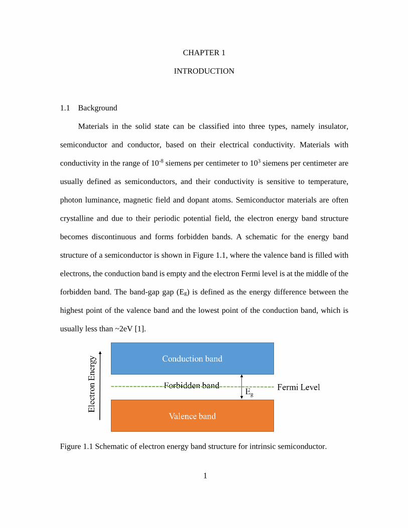
becomes discontinuous and forms forbidden bands. A schematic for the energy band
structure of a semiconductor is shown in Figure 1.1, where the valence band is filled with
electrons, the conduction band is empty and the electron Fermi level is at the middle of the
forbidden band. The band-gap gap (Eg) is defined as the energy difference between the
highest point of the valence band and the lowest point of the conduction band, which is
usually less than ~2eV [1].
Figure 1.1 Schematic of electron energy band structure for intrinsic semiconductor.
1
When the temperature is higher than 0K or there is photon luminance, some of the
electrons are excited from the valence band to the conduction band. Thus, electrons in the
conduction band or empty states in the valence band (holes) can move under the influence
of an external electric field and the material becomes conductive. However, the number of
excited electrons is usually relatively small at room temperature and the conductivity is
still low compared to conductors such as metals.
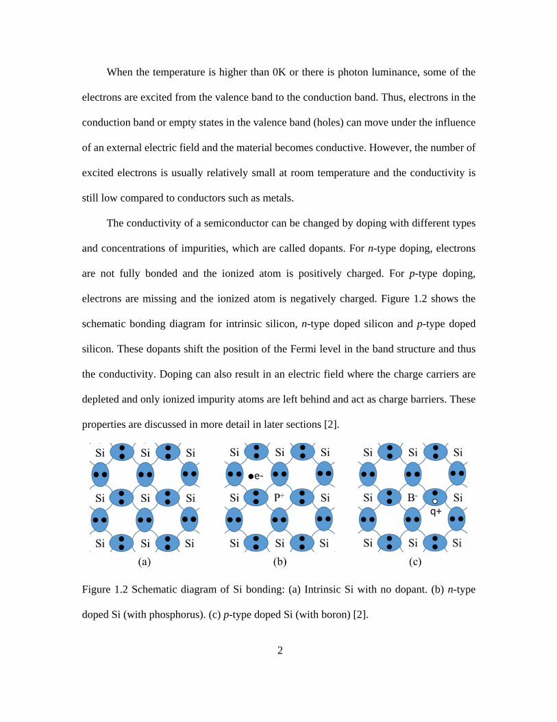
The conductivity of a semiconductor can be changed by doping with different types
and concentrations of impurities, which are called dopants. For n-type doping, electrons
are not fully bonded and the ionized atom is positively charged. For p-type doping,
electrons are missing and the ionized atom is negatively charged. Figure 1.2 shows the
schematic bonding diagram for intrinsic silicon, n-type doped silicon and p-type doped
silicon. These dopants shift the position of the Fermi level in the band structure and thus
the conductivity. Doping can also result in an electric field where the charge carriers are
depleted and only ionized impurity atoms are left behind and act as charge barriers. These
properties are discussed in more detail in later sections [2].
Figure 1.2 Schematic diagram of Si bonding: (a) Intrinsic Si with no dopant. (b) n-type
doped Si (with phosphorus). (c) p-type doped Si (with boron) [2].
2
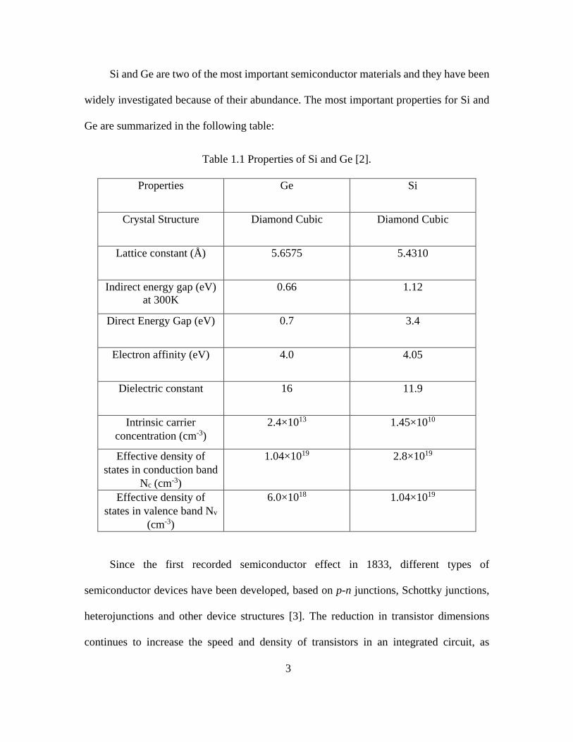
Si and Ge are two of the most important semiconductor materials and they have been
widely investigated because of their abundance. The most important properties for Si and
Ge are summarized in the following table:
Table 1.1 Properties of Si and Ge [2].
Properties Ge Si
Crystal Structure Diamond Cubic Diamond Cubic
Lattice constant (Å) 5.6575 5.4310
Indirect energy gap (eV) at 300K
0.66 1.12
Direct Energy Gap (eV) 0.7 3.4
Electron affinity (eV) 4.0 4.05
Dielectric constant 16 11.9
Intrinsic carrier concentration (cm-3)
2.4×10¹³ 1.45×10¹⁰
Effective density of states in conduction band
Nc (cm-3)
1.04×10¹⁹ 2.8×10¹⁹
Effective density of states in valence band Nv
(cm-3)
6.0×10¹⁸ 1.04×10¹⁹
Since the first recorded semiconductor effect in 1833, different types of
semiconductor devices have been developed, based on p-n junctions, Schottky junctions,
heterojunctions and other device structures [3]. The reduction in transistor dimensions
continues to increase the speed and density of transistors in an integrated circuit, as
3
predicted by Moore’s law [4]. The traditional Si-based top-down approach has scaled down
to 18nm (Logic Half-Pitch) in 2013 [5]. However, this approach becomes more and more
challenging as photolithography reaches the diffraction limit and alternative device
geometries are needed [6]. Nanowires (NWs) are one of the most promising nanoscale
device structures for future applications. Instead of top-down fabrication, NW growth
utilizes a bottom-up self-assembly approach and thus provides better size control, for
example, by controlling the size of the metal catalyst particles used for NW growth in the
vapor-liquid-solid growth method [7]. Reproducible electronic properties with high yield
can be easily achieved using this type of synthesis for large-scale integrated systems [8].
Moreover, by changing the components during growth, different compositions, dopant
types and concentrations, as well as radial and axial heterostructures can be produced,
making it possible to achieve different band alignments and device geometries for different
applications as well as 3D device integration [9,10]. The NW geometry can also reduce the
density of dislocations caused by lattice mismatch between materials, thus forming
crystalline structures that reduce interface scattering and result in higher mobility [11-13].
Due to the one-dimensional geometry, the NW structure is also an ideal platform for
quantum physics experiments [14]. The large surface-to-volume ratio significantly changes
the transistor properties due to surface effects so that they can also be used as novel
chemical environment sensors [15].
Control of dopant profiles in Si NWs has enabled promising applications for
nanoscale electronic devices, such as sensors [16] and field-effect transistors [12]. The
growth of radial heterostructures has been achieved in Ge/Si, Si/Ge [9,13,17] and p-Si/n-
CdS [18] core/shell NWs, Si/Ge/Si [17] and n-GaN/InGaN/p-GaN [19] core/multishell
4
NWs. Axial Si/Ge heterojunctions NW have also been realized using vapor-liquid-solid
(VLS) [20] and vapor-solid-solid (VSS) methods [10]. The Ge/Si core/shell NW structure
has been reported to form a high-mobility hole gas due to its type-II band alignment [21]
and can be integrated to operate as a field-effect transistor (FET) [13]. Different electronic
transport properties have been achieved by growing Ge NWs on Si pillars using substrate
etching and by changing dopant profiles [22].
In order to understand the electronic transport properties and to improve the
performance of semiconductor devices, it is important to determine the electrostatic
potential distribution and the concentration of electrically active dopant across the device
structure. These properties become even more important as device dimensions approach
the nanometer scale since quantum effects and surface area play more important roles.
Although theoretical calculation and simulations enable prediction of these device
properties, experimental measurements play a determining role, which imposes a challenge
on the measurement method. The research of this dissertation involves the use of off-axis
electron holography to characterize the electrostatic field profile across NW devices with
nanoscale spatial resolution, as well as comparisons with simulations to determine the
active dopants and trapped charges in the nanostructures.
1.2 Charge Distribution and Band Alignment in Semiconductors
1.2.1 p-n Junction
A p-n junction is formed by making contact between a p-type semiconductor and an
n-type semiconductor. If the p-type and n-type regions are made of the same material, the
junction is called homojunction. When the semiconductor materials are different, the
5
junction is called heterojunction. The heterojunction is discussed later. The p-n junction
has unique electrical characteristics which can be used for rectifiers, light emitter diodes,
solar cells and tunnel effect transistors [23-25]. Most semiconductor devices include at
least one p-n junction and thus their characteristics are directly linked to the p-n junction
properties.
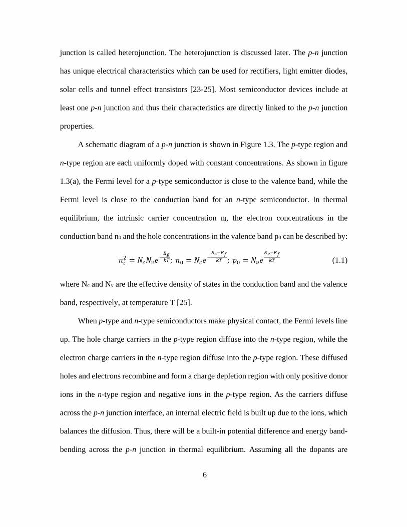
A schematic diagram of a p-n junction is shown in Figure 1.3. The p-type region and
n-type region are each uniformly doped with constant concentrations. As shown in figure
1.3(a), the Fermi level for a p-type semiconductor is close to the valence band, while the
Fermi level is close to the conduction band for an n-type semiconductor. In thermal
equilibrium, the intrinsic carrier concentration ni, the electron concentrations in the
conduction band n0 and the hole concentrations in the valence band p0 can be described by:
𝑛𝑛𝑖𝑖2 = 𝑁𝑁𝑐𝑐𝑁𝑁𝑣𝑣𝑒𝑒−𝐸𝐸𝑔𝑔𝑘𝑘𝑘𝑘; 𝑛𝑛0 = 𝑁𝑁𝑐𝑐𝑒𝑒
−𝐸𝐸𝑐𝑐−𝐸𝐸𝑓𝑓𝑘𝑘𝑘𝑘 ; 𝑝𝑝0 = 𝑁𝑁𝑣𝑣𝑒𝑒
𝐸𝐸𝑣𝑣−𝐸𝐸𝑓𝑓𝑘𝑘𝑘𝑘 (1.1)
where Nc and Nv are the effective density of states in the conduction band and the valence
band, respectively, at temperature T [25].
When p-type and n-type semiconductors make physical contact, the Fermi levels line
up. The hole charge carriers in the p-type region diffuse into the n-type region, while the
electron charge carriers in the n-type region diffuse into the p-type region. These diffused
holes and electrons recombine and form a charge depletion region with only positive donor
ions in the n-type region and negative ions in the p-type region. As the carriers diffuse
across the p-n junction interface, an internal electric field is built up due to the ions, which
balances the diffusion. Thus, there will be a built-in potential difference and energy band-
bending across the p-n junction in thermal equilibrium. Assuming all the dopants are
6
ionized and that there are no free carriers in the depletion region, then the built-in potential
Vbi and the depletion region length W can be calculated using the following equations:
𝑉𝑉𝑏𝑏𝑖𝑖 = 𝑘𝑘𝑘𝑘𝑒𝑒
ln �𝑁𝑁𝑎𝑎𝑁𝑁𝑑𝑑𝑛𝑛𝑖𝑖2 � ;𝑊𝑊 = (2𝜀𝜀𝑠𝑠𝑉𝑉𝑏𝑏𝑖𝑖
𝑒𝑒�𝑁𝑁𝑎𝑎+𝑁𝑁𝑑𝑑𝑁𝑁𝑎𝑎𝑁𝑁𝑑𝑑
�)1/2 (1.2)
Figure 1.3 Schematic diagram of a p-n junction: (a) Energy band diagrams of p-type and
n-type semiconductors. (b) Energy band diagram of a p-n junction in thermal equilibrium.
(c) Depletion region of a p-n junction [26].
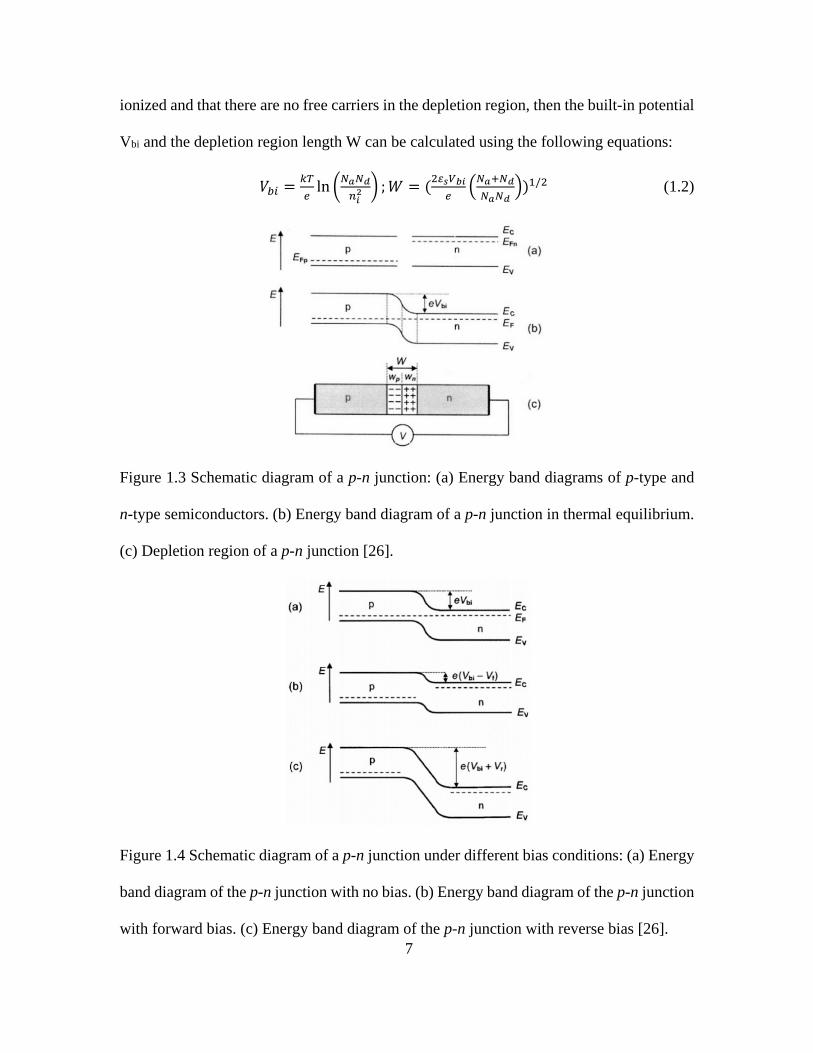
Figure 1.4 Schematic diagram of a p-n junction under different bias conditions: (a) Energy
band diagram of the p-n junction with no bias. (b) Energy band diagram of the p-n junction
with forward bias. (c) Energy band diagram of the p-n junction with reverse bias [26]. 7

where εs is the dielectric permittivity, and Nd and Na are the dopant concentration for donor
and acceptor, respectively [25].
The band diagram of a p-n junction under different bias conditions is shown in Figure
1.4. At zero bias, if there is thermal emission or photon luminance with energy higher than
Eg, electrons transfer from the valence band to the conduction band in the depletion region
and form electron-hole pairs. Before recombination, these electron-hole pairs can be
accelerated by the internal electric field, become separated and form current across the
junction, which is the basic operating principle of the solar cell. At forward bias, the built-
in potential or barrier across the p-n junction is lowered. The applied electric field is
opposite to the internal electric field due to diffusion, and thus electrons (holes) in the n-
type (p-type) region diffuse across the depletion region into the p-type (n-type) region and
increase the minority carrier density, again forming current across the p-n junction. If the
injected minority carriers recombine with majority carriers in the depletion region or in the
neutral region, a photon with energy of Eg might be emitted because the electron in the
conduction band transfers to the valence band and releases energy. This effect is used as
the basis for light-emitting diodes. At reverse bias, the built-in potential or barrier across
the p-n junction is higher. The applied electric field is in the same direction as the internal
electric field due to diffusion. The depletion region becomes larger because of the stronger
electric field and the higher barrier stops carriers from moving. Therefore, there will be no
current through the p-n junction until the junction breaks down due to the Zener effect or
an avalanche effect. The combined I-V curve characteristics for forward or reverse bias
conditions are useful for rectifiers or current multipliers. The Zener effect happens when
the p-n junction is heavily doped. Under reverse-bias conditions, the valence band in the
8
p-type region is close to the conduction band in the n-type region. The p-n junction
depletion region is short and thus electrons can tunnel through the p-n junction from the p-
type valence band to the n-type conduction band and induce current. This effect is also
used as the basis for the tunneling effect transistor. The avalanche effect occurs when the
electron-hole pairs generated from thermal emission in the depletion region are accelerated
across the electric field in the depletion region, they hit other electrons and form more
electron-hole pairs, and thus induce current [2,23-25].
1.2.2 Metal Semiconductor Contact
There are two type of contacts formed between a metal and a semiconductor: ohmic
contacts and Schottky contacts. The ohmic contact shows a characteristic linear I-V curve,
while the Schottky contact shows a characteristic rectifying-effect I-V curve. Both contact
types have important applications in semiconductor devices and it is useful to summarize
here their transport properties because of their presence in the NWs that have been studied
in this dissertation research.
1.2.2.1 Schottky Contact
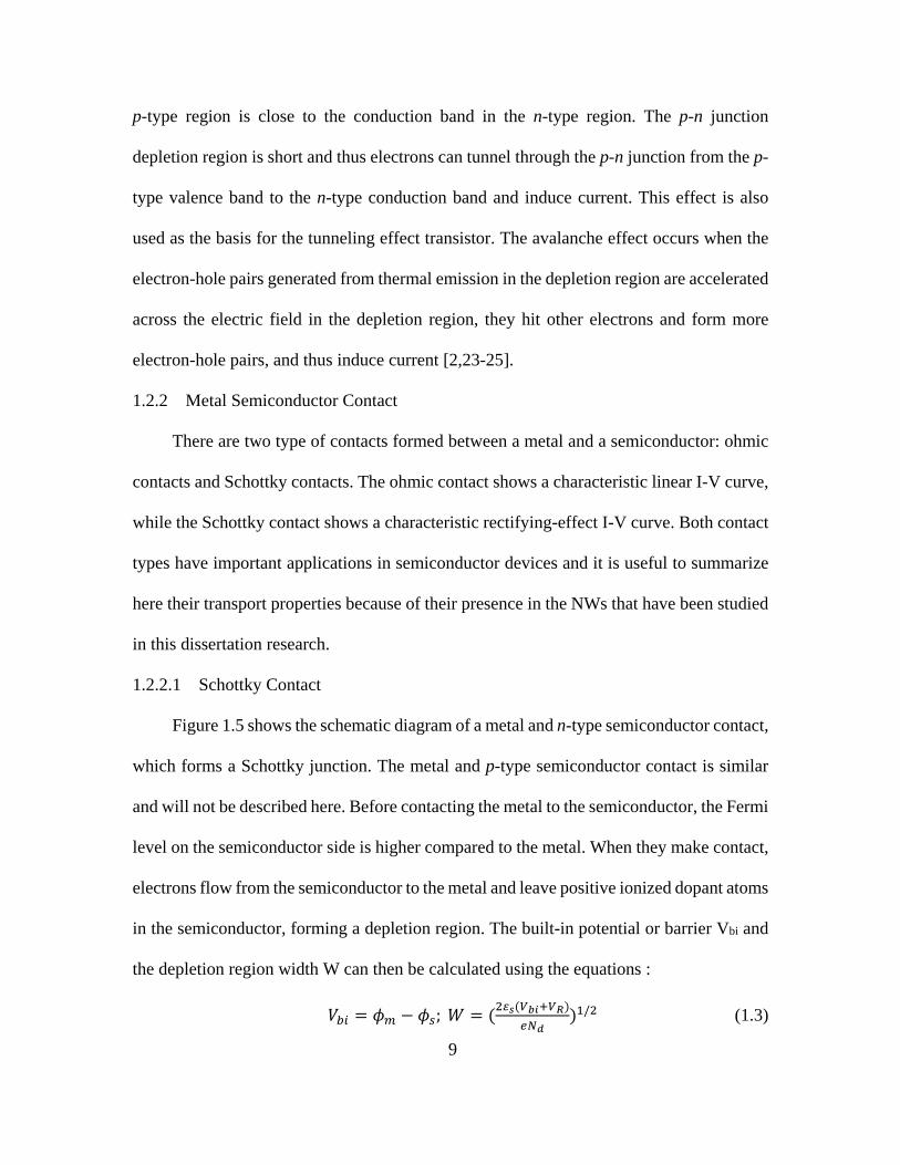
Figure 1.5 shows the schematic diagram of a metal and n-type semiconductor contact,
which forms a Schottky junction. The metal and p-type semiconductor contact is similar
and will not be described here. Before contacting the metal to the semiconductor, the Fermi
level on the semiconductor side is higher compared to the metal. When they make contact,
electrons flow from the semiconductor to the metal and leave positive ionized dopant atoms
in the semiconductor, forming a depletion region. The built-in potential or barrier Vbi and
the depletion region width W can then be calculated using the equations :
𝑉𝑉𝑏𝑏𝑖𝑖 = 𝜙𝜙𝑚𝑚 − 𝜙𝜙𝑠𝑠; 𝑊𝑊 = (2𝜀𝜀𝑠𝑠(𝑉𝑉𝑏𝑏𝑖𝑖+𝑉𝑉𝑅𝑅)𝑒𝑒𝑁𝑁𝑑𝑑
)1/2 (1.3)
9
where VR is the reverse bias, Nd is the semiconductor dopant concentration, and εs is
dielectric permittivity [27]. Some typical metal work functions are shown in table 1.2.
Figure 1.5 Schematic diagram of a Schottky contact: (a) Energy band diagram of metal and
p-type semiconductor before contact. (b) Energy band diagram of Schottky contact. ϕm is
work function for metal, ϕs and χ are work function and electron affinity, respectively, for
semiconductor [26].
Table 1.2 Work functions of common metal contacts.
Metal Work function(V)
Au 5.1
W 4.55
Pt 5.65
When forward bias is applied, the Fermi level on the metal side will be lower and the
barrier height is reduced. Electrons can flow easily from semiconductor to metal and form
current through thermal emission. When reverse bias is applied, the Fermi level on the 10
metal side will be higher and the barrier height as well as the depletion region width are
increased. There is no current through the Schottky contact under this condition. Therefore,
the Schottky contact shows similar rectifying effect as the p-n junction, although the
current across the Schottky contact is mainly due to majority carriers [25].
1.2.2.2 Ohmic Contact
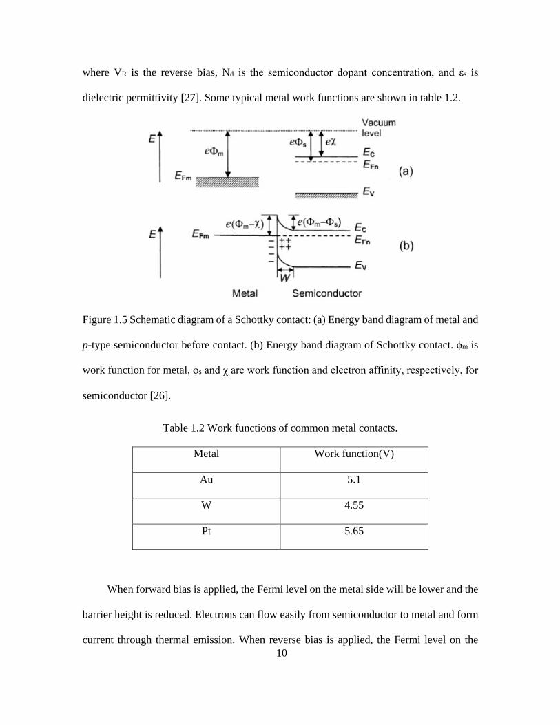
Figure 1.6 shows the schematic diagram of an ohmic contact between a metal and an
n-type semiconductor. The metal and p-type ohmic contact is similar and is not described
here. In this case, the Fermi level on the metal side is higher than for the semiconductor
and electrons flow from metal to semiconductor. Because of these extra electrons, the
semiconductor becomes more n-type and there are extra surface electrons at the metal-
semiconductor interface. As positive bias is applied to the metal, electrons flow easily to
the metal from the semiconductor. When negative bias is applied, electrons can also go
easily through the barrier and flow to the semiconductor. Therefore, the current through
the contact is proportional to the voltage [25].
11
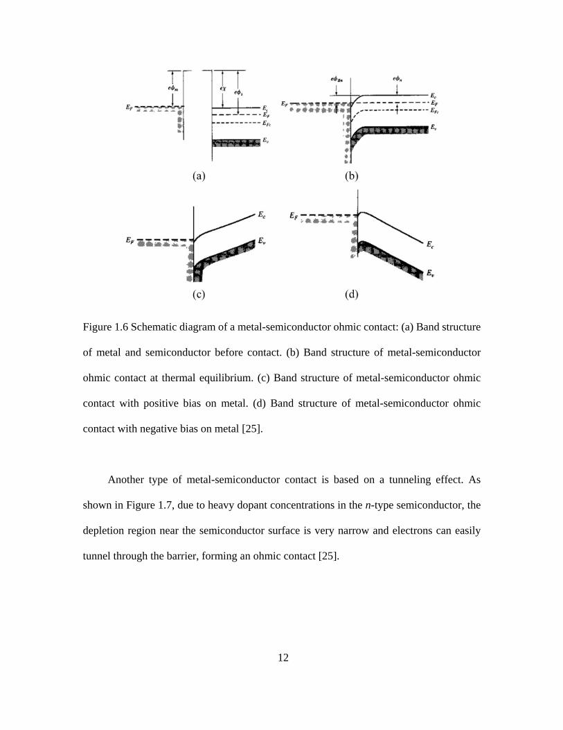
Figure 1.6 Schematic diagram of a metal-semiconductor ohmic contact: (a) Band structure
of metal and semiconductor before contact. (b) Band structure of metal-semiconductor
ohmic contact at thermal equilibrium. (c) Band structure of metal-semiconductor ohmic
contact with positive bias on metal. (d) Band structure of metal-semiconductor ohmic
contact with negative bias on metal [25].
Another type of metal-semiconductor contact is based on a tunneling effect. As
shown in Figure 1.7, due to heavy dopant concentrations in the n-type semiconductor, the
depletion region near the semiconductor surface is very narrow and electrons can easily
tunnel through the barrier, forming an ohmic contact [25].
12
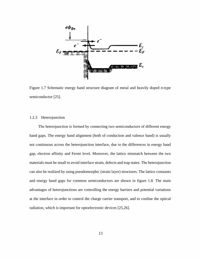
Figure 1.7 Schematic energy band structure diagram of metal and heavily doped n-type
semiconductor [25].
1.2.3 Heterojunction
The heterojunction is formed by connecting two semiconductors of different energy
band gaps. The energy band alignment (both of conduction and valence band) is usually
not continuous across the heterojunction interface, due to the differences in energy band
gap, electron affinity and Fermi level. Moreover, the lattice mismatch between the two
materials must be small to avoid interface strain, defects and trap states. The heterojunction
can also be realized by using pseudomorphic (strain layer) structures. The lattice constants
and energy band gaps for common semiconductors are shown in figure 1.8. The main
advantages of heterojunctions are controlling the energy barriers and potential variations
at the interface in order to control the charge carrier transport, and to confine the optical
radiation, which is important for optoelectronic devices [25,26].
13
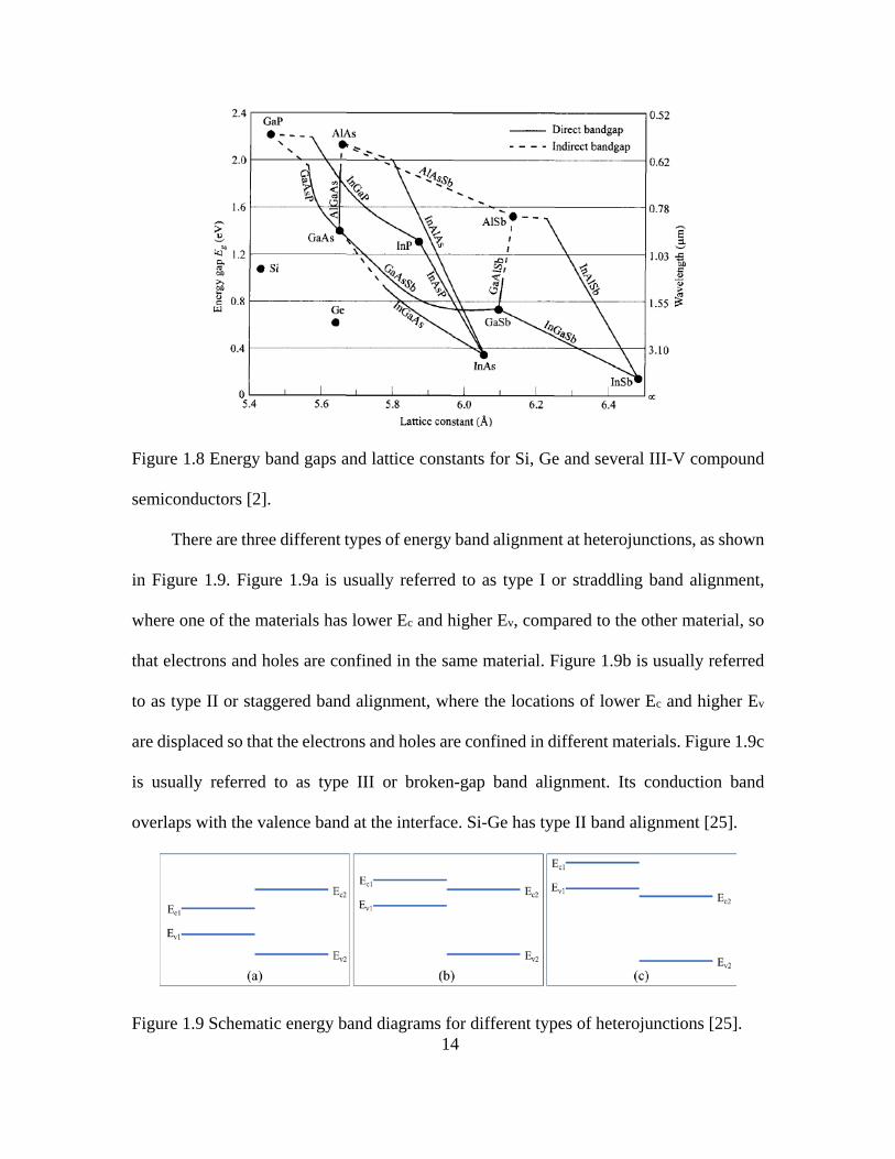
Figure 1.8 Energy band gaps and lattice constants for Si, Ge and several III-V compound
semiconductors [2].
There are three different types of energy band alignment at heterojunctions, as shown
in Figure 1.9. Figure 1.9a is usually referred to as type I or straddling band alignment,
where one of the materials has lower Ec and higher Ev, compared to the other material, so
that electrons and holes are confined in the same material. Figure 1.9b is usually referred
to as type II or staggered band alignment, where the locations of lower Ec and higher Ev
are displaced so that the electrons and holes are confined in different materials. Figure 1.9c
is usually referred to as type III or broken-gap band alignment. Its conduction band
overlaps with the valence band at the interface. Si-Ge has type II band alignment [25].
Figure 1.9 Schematic energy band diagrams for different types of heterojunctions [25]. 14
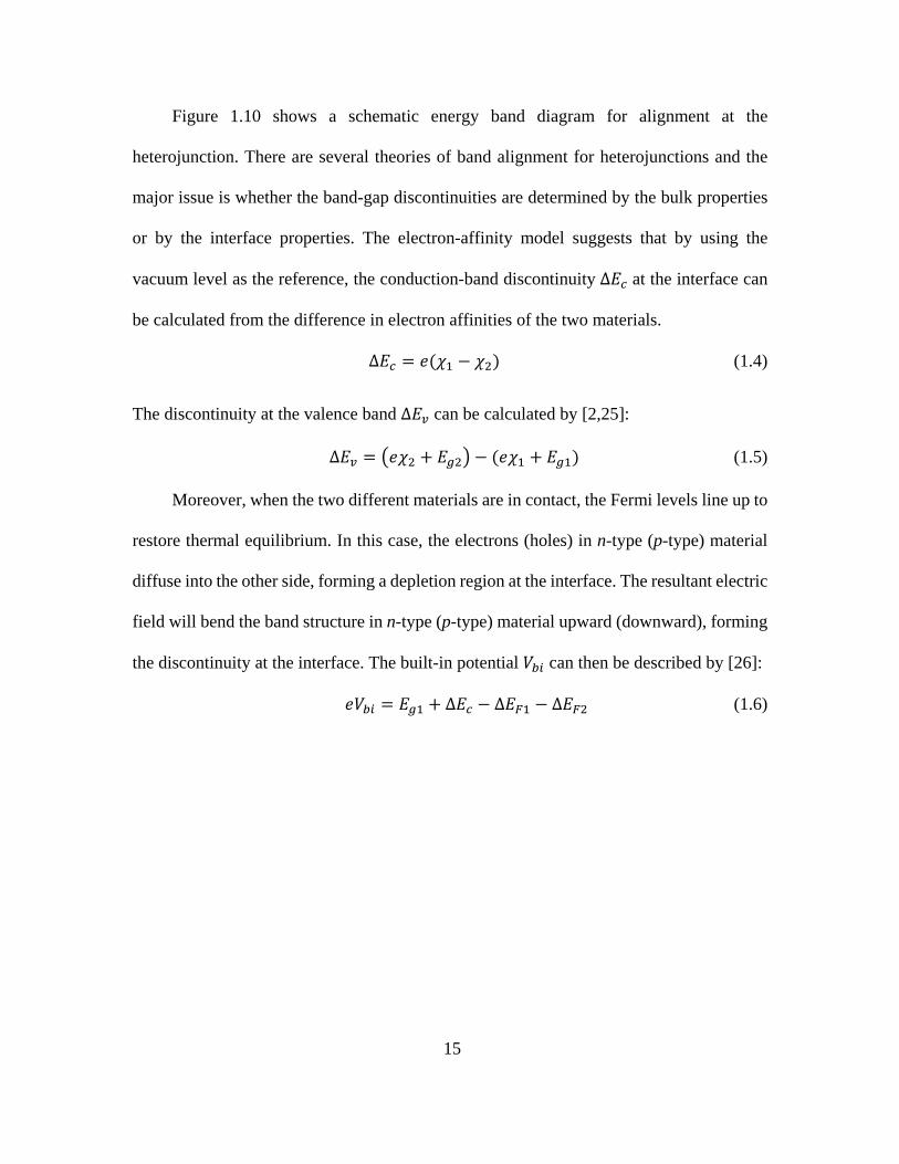
Figure 1.10 shows a schematic energy band diagram for alignment at the
heterojunction. There are several theories of band alignment for heterojunctions and the
major issue is whether the band-gap discontinuities are determined by the bulk properties
or by the interface properties. The electron-affinity model suggests that by using the
vacuum level as the reference, the conduction-band discontinuity ∆𝐸𝐸𝑐𝑐 at the interface can
be calculated from the difference in electron affinities of the two materials.
∆𝐸𝐸𝑐𝑐 = 𝑒𝑒(𝜒𝜒1 − 𝜒𝜒2) (1.4)
The discontinuity at the valence band ∆𝐸𝐸𝑣𝑣 can be calculated by [2,25]:
∆𝐸𝐸𝑣𝑣 = �𝑒𝑒𝜒𝜒2 + 𝐸𝐸𝑔𝑔2� − (𝑒𝑒𝜒𝜒1 + 𝐸𝐸𝑔𝑔1) (1.5)
Moreover, when the two different materials are in contact, the Fermi levels line up to
restore thermal equilibrium. In this case, the electrons (holes) in n-type (p-type) material
diffuse into the other side, forming a depletion region at the interface. The resultant electric
field will bend the band structure in n-type (p-type) material upward (downward), forming
the discontinuity at the interface. The built-in potential 𝑉𝑉𝑏𝑏𝑖𝑖 can then be described by [26]:
𝑒𝑒𝑉𝑉𝑏𝑏𝑖𝑖 = 𝐸𝐸𝑔𝑔1 + ∆𝐸𝐸𝑐𝑐 − ∆𝐸𝐸𝐹𝐹1 − ∆𝐸𝐸𝐹𝐹2 (1.6)
15
Figure 1.10 Schematic energy band diagram for heterojunctions before and after contact
[26].
1.3 Growth of Semiconductor Nanostructures
1.3.1 Epitaxial Growth Techniques
Semiconductor nanowires can be grown by a wide variety of epitaxial growth
techniques, which include chemical-vapor deposition (CVD) and molecular-beam expitaxy
(MBE).
CVD is a technique that enables thin film growth on a suitable substrate material
using chemical reaction of vapor-phase precursors to form the desired deposit. The
substrate is usually used as the seed crystal, and because it uses a chemical reaction as the
deposit-forming mechanism, the growth temperature can be much lower relative to the thin
film melting point. The conventional CVD process can be described as follows: (a) the
16
precursors are evaporated and transported from the bulk gas region into the reactor chamber,
using carrier gas; (b) reactive intermediates and gaseous by-products are produced from
gas-phase precursor reactions; (c) reactants are transported and adsorbed by the substrate
surface; (d) reactants diffuse to the growth site, and the thin film is grown by surface
nucleation and chemical reactions; (e) the remaining decomposition materials are desorbed
and transported out of the chamber [1,28]. The Si, Ge, Si/Ge heterojunction NWs
characterized in Chapters 4, 5 and 6 were gown using a cold-wall CVD reactor using the
VLS growth mechanism described below.
MBE is an epitaxial growth technique that uses the interaction of molecular or atomic
beams on a heated crystal substrate surface under ultrahigh-vacuum condition. The growth
rate in MBE is usually low (~1 monolayer per second) and this technique thus enables
precise control of film thicknesses, compositions, dopants, and morphology. The absence
of carrier gas and ultrahigh-vacuum can help to reduce the level of impurities during
growth. Moreover, reflection-high-energy electron diffraction can be used for monitoring
the crystal layer growth for better structure and thickness control. The MBE growth process
can be described as follows: (a) solid-source atoms or homo-atomic molecules of the
growth material in separate quasi-Knudsen diffusion cells are evaporated, transported and
condensed on the heated crystal substrate surface. (b) atoms diffuse on the surface and react
with other atoms to form the epitaxial layer [29,30]. The ZnTe thin film characterized in
Chapter 3 was grown using the MBE method.
1.3.2 Nanowire Growth
Three different methods are most commonly used for growing freestanding NWs
originating from the substrate surface: these are vapor-liquid-solid (VLS) [20,31-33],
17
vapor-solid-solid (VSS) [10,34] and solution-liquid-solid (SLS) [35-37] growth. The VLS
growth has been extensively studied and it is widely used due to its simplicity and
versatility. The method was firstly suggested by Wagner and Ellis to deposit micrometer-
sized Si whiskers with gold impurities [31]. Figure 1.11 shows the schematic diagram of
the VLS growth procedure. For the growth of Si NWs on Si substrates, gold particles are
deposited on the Si substrate surface as catalysts. The substrate is heated up and precursor
vapor of the growth species (SiH4) is transported to the CVD chamber by H2 carrier gas.
SiH4 vapor decomposes at the Au particle surface and eutectic liquid-alloy droplets of AuSi
are formed after adsorbing Si atoms. The eutectic temperature of the AuSi alloy is usually
much lower than the melting point of Au. The residual hydrogen by-product is taken away
with the carrier gas, while Si atoms in the catalyst diffuse from the catalyst surface to the
Au/Si substrate liquid/solid interface driven by the concentration gradient. When more and
more Si is adsorbed into the catalyst, the eutectic alloy eventually becomes supersaturated.
In order to restore equilibrium concentration, the Si component in AuSi alloy starts to
precipitate at the liquid-solid interface, crystallize and form the NW structure. The AuSi
alloy is pushed upwards as extra NW structure grows between the catalyst and the substrate.
As the growth process continues, more Si atoms diffuse from the AuSi catalyst surface to
the catalyst-NW liquid-solid interface and crystallize, making the NW longer. Therefore,
the size of the Au seed controls the NW diameter, while growth time controls the NW
length [35]. VSS growth can also occur along the NW surface, depending on the growth
temperature, and changes the NW into a tapered shape [32,33]. During VLS growth, the
Au particles act as catalyst as well as reservoir. In order to grow axial heterojunction NW,
the precursor vapor has to be changed from one growth species to another. Because of the
18
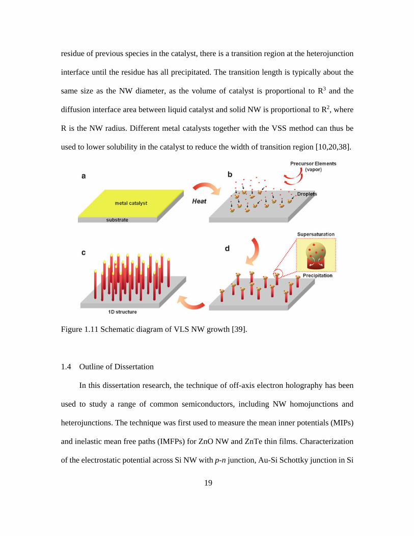
residue of previous species in the catalyst, there is a transition region at the heterojunction
interface until the residue has all precipitated. The transition length is typically about the
same size as the NW diameter, as the volume of catalyst is proportional to R3 and the
diffusion interface area between liquid catalyst and solid NW is proportional to R2, where
R is the NW radius. Different metal catalysts together with the VSS method can thus be
used to lower solubility in the catalyst to reduce the width of transition region [10,20,38].
Figure 1.11 Schematic diagram of VLS NW growth [39].
1.4 Outline of Dissertation
In this dissertation research, the technique of off-axis electron holography has been
used to study a range of common semiconductors, including NW homojunctions and
heterojunctions. The technique was first used to measure the mean inner potentials (MIPs)
and inelastic mean free paths (IMFPs) for ZnO NW and ZnTe thin films. Characterization
of the electrostatic potential across Si NW with p-n junction, Au-Si Schottky junction in Si
19
NW, Si-Ge axial heterojunction NW, as well as Ge/LixGe core/shell NW structure were
also performed using this technique and compared with SilvacoTM device simulation and/or
Poisson equation calculation to determine the active dopant concentrations and trapped
charges in the nanostructures. Transmission electron microscopy (TEM), scanning
transmission electron microscopy (STEM) and electron-energy-loss spectrum (EELS)
technique were also used to characterize the morphology and structure of the
nanostructures, while atom probe tomography (APT) was used to determine the total
dopant concentrations and distributions in Si-Ge axial heterojunction NWs.
In Chapter 2, the background, theory and experiment setup for off-axis electron
holography are briefly described. An outline procedure for electron hologram
reconstruction is discussed, followed by reconstructed phase and thickness images
interpretation, definition and calculation of MIPs. The basis of EELS and high-angle
annular-dark-field imaging (HAADF) are also briefly discussed. Finally, the sample
preparation methods used in this thesis are described.
In Chapter 3, the morphology of ZnO NWs characterized using TEM is described.
The MIP and IMFP are measured using off-axis electron holography and applied to ZnO
thin films for the measurement of thickness. MIP and IMFP of ZnTe thin films are also
measured by combining off-axis electron holography and CBED thickness measurements.
The dynamic effects due to tilting and thickness are systematically studied for ZnTe thin
film by using simulations. Electrostatic potential across p-n junction in ZnTe thin film is
then measured using electron holography.
In Chapter 4, measurement of electrostatic potential across p-n junction and Schottky
junction in Si NW is performed using off axis electron holography. The built-in potential
20
is then extracted and compared with SilvacoTM simulations to determine the active dopant
concentrations. The influence of surface charge, transition region length and charging in
the Au catalyst particle are systematically studied by comparing experiment with
simulation results.
In Chapter 5, TEM and STEM HAADF are used to characterize the Si-Ge axial
heterojunction NW interface, and geometry phase analysis is performed based on HAADF
images. Characterization of electrostatic potential across Si-Ge axial heterojunction NWs
with/without in situ biasing using off-axis electron holography is presented. APT is also
performed to measure the total dopant concentrations and distributions. The SilvacoTM
simulations with/without biasing are compared with holography and APT results to
determine the active dopant amounts in Si-Ge NW.
In Chapter 6, the lithiation of Ge NWs to form Ge/LixGe core/shell structure is
outlined. The core/shell structure was characterized using TEM, STEM and EELS.
Electron holography experiments were then performed on the core/shell structure during
the lithiation process to measure the electrostatic potential. The measured potential was
compared with Poisson equation calculation to determine the amount of trapped charge in
the core/shell structure.
In Chapter 7, the important results and conclusions in the thesis are summarized, and
possible topics for further investigation are briefly described.
21
References
[1] S. M. Sze, Semiconductor devices, physics and technology, 2nd ed. Wiley, New York, (2002).
[2] S. M. Sze, Physics of semiconductor devices, 2nd ed. Wiley, New York, (1981).
[3] M. Faraday, Experimental researches in electricity. R. and J.E. Taylor, London, (1839).
[4] G. E. Moore, Proceedings of the IEEE 86 82 (1998).
[5] International Technology Roadmap for Semiconductors 2013, available online at http://www.itrs.net.
[6] R. Agarwal, Small 4 1872 (2008).
[7] Y. Wu, Y. Cui, L. Huynh, C. J. Barrelet, D. C. Bell, and C. M. Lieber, Nano letters 4 433 (2004).
[8] W. Lu, P. Xie, and C. M. Lieber, IEEE Transactions on Electron Devices 55 2859 (2008).
[9] W. Lu, J. Xiang, B. P. Timko, Y. Wu, and C. M. Lieber, Proc. Nat. Acad. Sci. 102 10046 (2005).
[10] C. Y. Wen, M. C. Reuter, J. Bruley, J. Tersoff, S. Kodambaka, E. A. Stach, and F. M. Ross, Science 326 1247 (2009).
[11] V. Schmidt, H. Riel, S. Senz, S. Karg, W. Riess, and U. Gosele, Small 2 85 (2006).
[12] J. Goldberger, A. I. Hochbaum, R. Fan, and P. Yang, Nano letters 6 973 (2006).
[13] J. Xiang, W. Lu, Y. Hu, Y. Wu, H. Yan, and C. M. Lieber, Nature 441 489 (2006).
[14] Y. Hu, H. O. Churchill, D. J. Reilly, J. Xiang, C. M. Lieber, and C. M. Marcus, Nature nanotechnology 2 622 (2007).
[15] I. Kimukin, M. S. Islam, and R. S. Williams, Nanotechnology 17 S240 (2006).
[16] Y. Cui, Q. Wei, H. Park, and C. M. Lieber, Science 293 1289 (2001).
[17] L. J. Lauhon, M. S. Gudiksen, C. L. Wang, and C. M. Lieber, Nature 420 57 (2002).
[18] O. Hayden, A. B. Greytak, and D. C. Bell, Advanced Materials 17 701 (2005).
22
[19] F. Qian, Y. Li, S. Gradecak, D. L. Wang, C. J. Barrelet, and C. M. Lieber, Nano letters 4 1975 (2004).
[20] D. E. Perea, N. Li, R. M. Dickerson, A. Misra, and S. T. Picraux, Nano letters 11 3117 (2011).
[21] L. Li, D. J. Smith, E. Dailey, P. Madras, J. Drucker, and M. R. McCartney, Nano letters 11 493 (2011).
[22] L. Chen, W. Y. Fung, and W. Lu, Nano letters 13 5521 (2013).
[23] U. K. Mishra, J. Singh, Semiconductor device physics and design. Springer, Dordrecht, The Netherlands, (2008).
[24] S. Dimitrijev, Understanding semiconductor devices. Oxford University Press, New York, (2000).
[25] D. A. Neamen, Semiconductor physics and devices : basic principles, 2nd ed. Irwin, Chicago, (1997).
[26] B. G. Yacobi, Semiconductor materials : an introduction to basic principles. Kluwer Academic/Plenum Publishers, New York, (2003).
[27] D. A. Neamen, Semiconductor physics and devices : basic principles, 3rd ed. McGraw-Hill Higher Education, London, (2003).
[28] A. C. Jones, M. L. Hitchman, and Knovel (Firm), Chemical vapour deposition precursors, processes and applications. Royal Society of Chemistry, Cambridge, UK, (2009).
[29] J. Y. Tsao, Materials fundamentals of molecular beam epitaxy. Academic Press, Boston, (1993).
[30] M. A. Herman and H. Sitter, Molecular beam epitaxy : fundamentals and current status, 2nd, rev. and updated ed. Springer, New York, (1996).
[31] R. S. Wagner and W. C. Ellis, Applied Physics Letters 4 89 (1964).
[32] J. W. Dailey, J. Taraci, T. Clement, D. J. Smith, J. Drucker, and S. T. Picraux, J Appl Phys 96 7556 (2004).
[33] S. A. Dayeh, J. Wang, N. Li, J. Y. Huang, A. V. Gin, and S. T. Picraux, Nano letters 11 4200 (2011).
[34] Y.-C. Chou, C.-Y. Wen, M. C. Reuter, D. Su, E. A. Stach, and F. M. Ross, ACS Nano 6 6407 (2012).
23

[35] V. Schmidt, J. V. Wittemann, S. Senz, and U. Gösele, Advanced Materials 21 2681 (2009).
[36] M.-S. Kim and Y.-M. Sung, Chem Mater 25 4156 (2013).
[37] A. T. Heitsch, D. D. Fanfair, H.-Y. Tuan, and B. A. Korgel, J Am Chem Soc 130 5436 (2008).
[38] N. Li, T. Y. Tan, and U. Gösele, Applied Physics A 90 591 (2008).
[39] G.-C. Yi, Semiconductor Nanostructures for Optoelectronic Devices Processing, Characterization and Applications, Springer, Heidelberg, (2012).
24
CHAPTER 2
EXPERIMENTAL DETAILS
This chapter begins by providing some background and basic theory of off-axis
electron holography. The procedures used for hologram reconstruction are then described,
followed by details of reconstructed phase and thickness image interpretation, definition
and calculation of mean inner potential (MIP), and the experimental setup used for
recording electron holograms. The basis of electron-energy-loss spectroscopy (EELS) and
high-angle annular-dark-field (HAADF) imaging are also briefly discussed. Finally, the
sample preparation methods used for the research of this dissertation are illustrated.
2.1 Off-Axis Electron Holography
2.1.1 Introduction
Transmission electron microscopy (TEM) has been widely used to characterize
nanostructured materials. However, conventional TEM only provides spatial intensity
information about the sample, while the phase and amplitude of the specimen exit-surface
electron wavefunction are unavailable. The phase and amplitude information are directly
related to the electrostatic and magnetic fields of the sample, which are very important for
characterization of semiconducting and magnetic materials.
Electron holography is an electron-interference technique that can provide amplitude
and phase information about the sample with nanoscale spatial resolution [1]. By
overlapping the exit-surface electron wave with a reference wave, an interference pattern
(hologram) is formed, which allows retrieval of phase and amplitude information. The
25

technique of in-line holography was first proposed by Gabor as a method for correcting the
spherical aberration of the objective lens, thus overcoming the interpretable resolution limit
[2]. Leith and Upatnieks proposed the off-axis electron holography geometry as a way to
solve the twin-image problem of in-line holography, by overlapping the sample wave with
the vacuum (reference) wave using an electrostatic biprism [3]. However, the approach
was not effectively realized experimentally until the development of the field emission gun
(FEG). The FEG provides a high brightness and highly coherent electron beam, which is
critical for hologram interference [4,5]. The holograms were originally recorded on
photographic plates with non-linear response and the hologram reconstruction was done
using a light optical system [6]. The emergence of digital recording devices, such as the
slow-scan charge-coupled-device (CCD), which provides linear response over a wide
dynamical range of electron counts, has enabled quantitative reconstruction of electron
hologram using computer processing [7].
Since the initial realization of electron holography, the technique has been
extensively developed and over twenty different approaches for the realization of electron
holography have been identified [8]. Among these approaches, off-axis electron
holography with operation in the TEM imaging mode is the most widely used and most
successful technique for obtaining sample phase and amplitude information [9]. This setup
has been exclusively used for the holography experiments described in this dissertation
research.
2.1.2 Theory and Hologram Reconstruction
A schematic diagram for off-axis electron holography with operation in the TEM
imaging mode is shown in Figure 2.1. Parallel (coherent) electron illumination from the
26
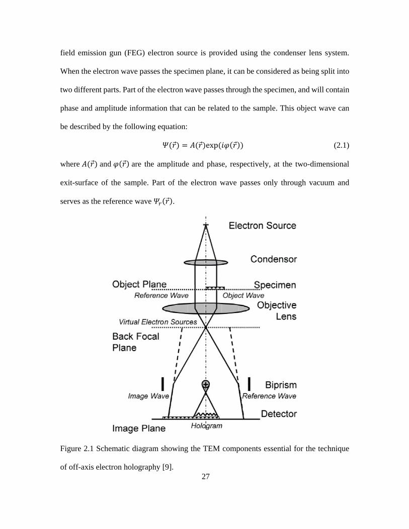
field emission gun (FEG) electron source is provided using the condenser lens system.
When the electron wave passes the specimen plane, it can be considered as being split into
two different parts. Part of the electron wave passes through the specimen, and will contain
phase and amplitude information that can be related to the sample. This object wave can
be described by the following equation:
𝛹𝛹(𝑟𝑟) = 𝐴𝐴(𝑟𝑟)exp (𝑖𝑖𝑖𝑖(𝑟𝑟)) (2.1)
where 𝐴𝐴(𝑟𝑟) and 𝑖𝑖(𝑟𝑟) are the amplitude and phase, respectively, at the two-dimensional
exit-surface of the sample. Part of the electron wave passes only through vacuum and
serves as the reference wave 𝛹𝛹𝑟𝑟(𝑟𝑟).
Figure 2.1 Schematic diagram showing the TEM components essential for the technique
of off-axis electron holography [9]. 27
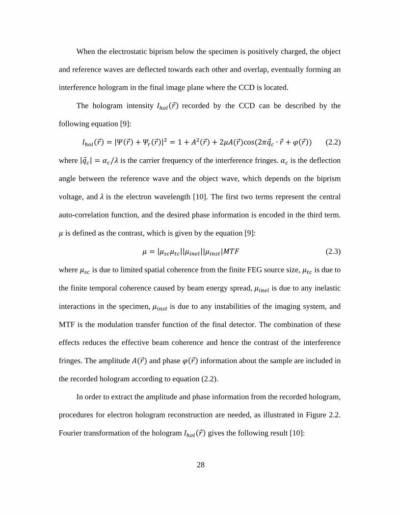
When the electrostatic biprism below the specimen is positively charged, the object
and reference waves are deflected towards each other and overlap, eventually forming an
interference hologram in the final image plane where the CCD is located.
The hologram intensity 𝐼𝐼ℎ𝑜𝑜𝑜𝑜(𝑟𝑟) recorded by the CCD can be described by the
following equation [9]:
𝐼𝐼ℎ𝑜𝑜𝑜𝑜(𝑟𝑟) = |𝛹𝛹(𝑟𝑟) + 𝛹𝛹𝑟𝑟(𝑟𝑟)|2 = 1 + 𝐴𝐴2(𝑟𝑟) + 2𝜇𝜇𝐴𝐴(𝑟𝑟)cos (2𝜋𝜋�⃗�𝑞𝑐𝑐 ∙ 𝑟𝑟 + 𝑖𝑖(𝑟𝑟)) (2.2)
where |�⃗�𝑞𝑐𝑐| = 𝛼𝛼𝑐𝑐/𝜆𝜆 is the carrier frequency of the interference fringes. 𝛼𝛼𝑐𝑐 is the deflection
angle between the reference wave and the object wave, which depends on the biprism
voltage, and 𝜆𝜆 is the electron wavelength [10]. The first two terms represent the central
auto-correlation function, and the desired phase information is encoded in the third term.
𝜇𝜇 is defined as the contrast, which is given by the equation [9]:
𝜇𝜇 = |𝜇𝜇𝑠𝑠𝑐𝑐𝜇𝜇𝑡𝑡𝑐𝑐||𝜇𝜇𝑖𝑖𝑛𝑛𝑒𝑒𝑜𝑜||𝜇𝜇𝑖𝑖𝑛𝑛𝑠𝑠𝑡𝑡|𝑀𝑀𝑀𝑀𝑀𝑀 (2.3)
where 𝜇𝜇𝑠𝑠𝑐𝑐 is due to limited spatial coherence from the finite FEG source size, 𝜇𝜇𝑡𝑡𝑐𝑐 is due to
the finite temporal coherence caused by beam energy spread, 𝜇𝜇𝑖𝑖𝑛𝑛𝑒𝑒𝑜𝑜 is due to any inelastic
interactions in the specimen, 𝜇𝜇𝑖𝑖𝑛𝑛𝑠𝑠𝑡𝑡 is due to any instabilities of the imaging system, and
MTF is the modulation transfer function of the final detector. The combination of these
effects reduces the effective beam coherence and hence the contrast of the interference
fringes. The amplitude 𝐴𝐴(𝑟𝑟) and phase 𝑖𝑖(𝑟𝑟) information about the sample are included in
the recorded hologram according to equation (2.2).
In order to extract the amplitude and phase information from the recorded hologram,
procedures for electron hologram reconstruction are needed, as illustrated in Figure 2.2.
Fourier transformation of the hologram 𝐼𝐼ℎ𝑜𝑜𝑜𝑜(𝑟𝑟) gives the following result [10]:
28
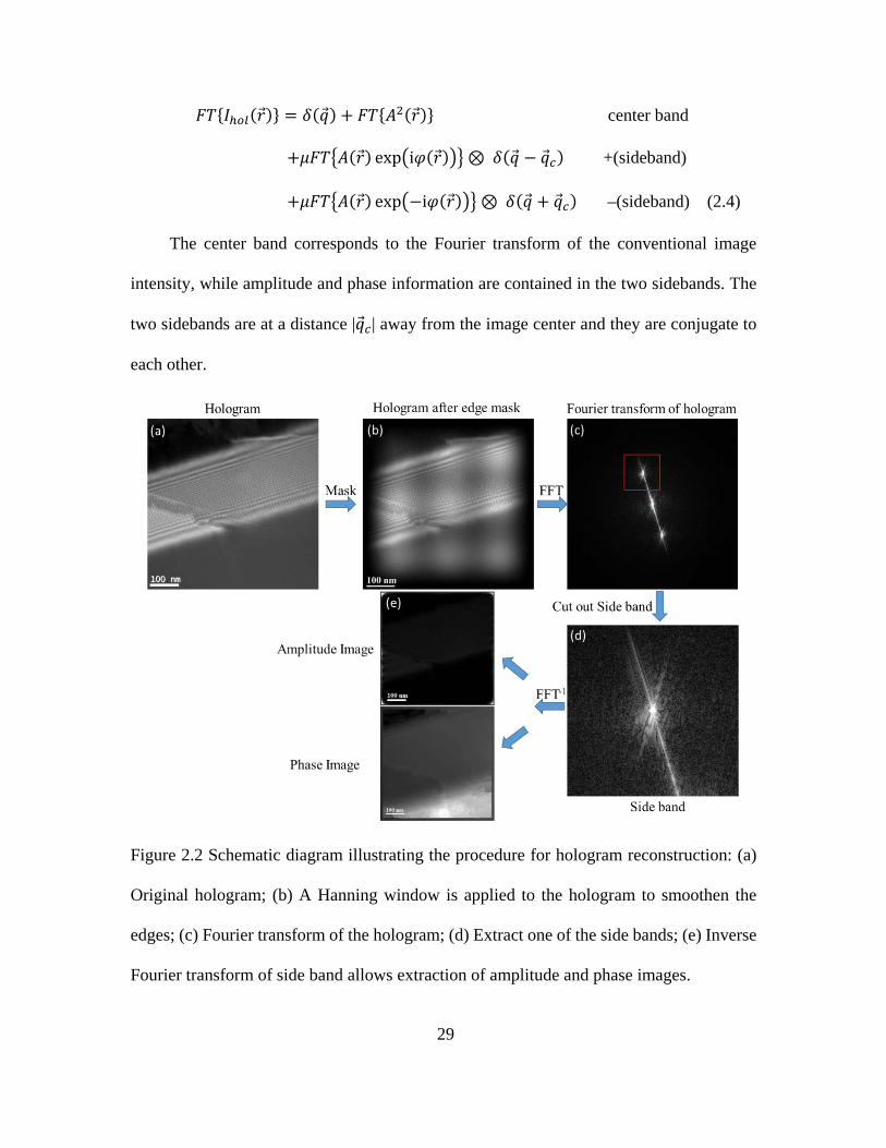
𝑀𝑀𝑀𝑀{𝐼𝐼ℎ𝑜𝑜𝑜𝑜(𝑟𝑟)} = 𝛿𝛿(�⃗�𝑞) + 𝑀𝑀𝑀𝑀{𝐴𝐴2(𝑟𝑟)} center band
+𝜇𝜇𝑀𝑀𝑀𝑀�𝐴𝐴(𝑟𝑟) exp�i𝑖𝑖(𝑟𝑟)�� ⊗ 𝛿𝛿(�⃗�𝑞 − �⃗�𝑞𝑐𝑐) +(sideband)
+𝜇𝜇𝑀𝑀𝑀𝑀�𝐴𝐴(𝑟𝑟) exp�−i𝑖𝑖(𝑟𝑟)�� ⊗ 𝛿𝛿(�⃗�𝑞 + �⃗�𝑞𝑐𝑐) –(sideband) (2.4)
The center band corresponds to the Fourier transform of the conventional image
intensity, while amplitude and phase information are contained in the two sidebands. The
two sidebands are at a distance |�⃗�𝑞𝑐𝑐 | away from the image center and they are conjugate to
each other.
Figure 2.2 Schematic diagram illustrating the procedure for hologram reconstruction: (a)
Original hologram; (b) A Hanning window is applied to the hologram to smoothen the
edges; (c) Fourier transform of the hologram; (d) Extract one of the side bands; (e) Inverse
Fourier transform of side band allows extraction of amplitude and phase images.
29
One of the sidebands is extracted, while the other parts are masked. The center of the
sideband is shifted to �⃗�𝑞 = �⃗�𝑞𝑐𝑐, to cancel the effect of the 𝛿𝛿(�⃗�𝑞 − �⃗�𝑞𝑐𝑐) term. An inverse Fourier
transform is then performed, which gives the complex exit-surface wavefunction:
𝛹𝛹𝑜𝑜𝑏𝑏𝑜𝑜(𝑟𝑟) = 𝜇𝜇𝐴𝐴(𝑟𝑟)exp (𝑖𝑖𝑖𝑖(𝑟𝑟)) (2.5)
The phase and amplitude of the image can then be calculated by extracting the real
part 𝛹𝛹𝑜𝑜𝑏𝑏𝑜𝑜(𝑟𝑟)𝑟𝑟𝑒𝑒 and the imaginary part 𝛹𝛹𝑜𝑜𝑏𝑏𝑜𝑜(𝑟𝑟)𝑖𝑖𝑚𝑚 of equation 2.5, as given by the following
equations:
𝑝𝑝ℎ𝑎𝑎𝑎𝑎𝑒𝑒 = 𝑖𝑖(𝑟𝑟) = arctan (𝛹𝛹𝑜𝑜𝑏𝑏𝑜𝑜(𝑟𝑟)𝑖𝑖𝑚𝑚𝛹𝛹𝑜𝑜𝑏𝑏𝑜𝑜(𝑟𝑟)𝑟𝑟𝑒𝑒� ) (2.6)
𝑎𝑎𝑎𝑎𝑝𝑝𝑎𝑎𝑖𝑖𝑎𝑎𝑎𝑎𝑎𝑎𝑒𝑒 = 𝜇𝜇𝐴𝐴(𝑟𝑟) = 𝑎𝑎𝑞𝑞𝑟𝑟𝑎𝑎(𝛹𝛹𝑜𝑜𝑏𝑏𝑜𝑜(𝑟𝑟)𝑟𝑟𝑒𝑒2 + 𝛹𝛹𝑜𝑜𝑏𝑏𝑜𝑜(𝑟𝑟)𝑖𝑖𝑚𝑚
2) (2.7)
The procedure described above can provide phase and amplitude information using
the object hologram only, but several practical details need attention during hologram
reconstruction before quantitative information can be obtained. A reference hologram as
well as the object hologram needs to be recorded. The hologram containing the sample
region of interest is termed the object hologram, while the hologram taken with vacuum
only but without the sample present is termed the reference hologram. The reference
hologram serves three purposes: (a) Define the center of side band �⃗�𝑞𝑐𝑐; (b) Cancel out any
distortions of the projector lenses and the CCD; and (c) Reduce the effect of Fresnel fringes
recorded in the hologram, which can cause continuous frequencies between the image
center and the sidebands in the Fourier transform.
After reconstruction of the reference hologram, the end result is:
𝛹𝛹𝑟𝑟𝑒𝑒𝑟𝑟(𝑟𝑟) = 𝜇𝜇𝐴𝐴𝑟𝑟𝑒𝑒𝑟𝑟(𝑟𝑟)exp (𝑖𝑖𝑖𝑖𝑟𝑟𝑒𝑒𝑟𝑟(𝑟𝑟)) (2.8)
30
The exit-surface wavefunction 𝛹𝛹𝑠𝑠𝑠𝑠𝑚𝑚𝑠𝑠𝑜𝑜𝑒𝑒(𝑟𝑟) can then be calculated using:
𝛹𝛹𝑠𝑠𝑠𝑠𝑚𝑚𝑠𝑠𝑜𝑜𝑒𝑒(𝑟𝑟) = 𝛹𝛹𝑜𝑜𝑏𝑏𝑜𝑜(𝑟𝑟)
𝛹𝛹𝑟𝑟𝑟𝑟𝑓𝑓(𝑟𝑟)= 𝐴𝐴𝑜𝑜𝑏𝑏𝑜𝑜(𝑟𝑟)
𝐴𝐴𝑟𝑟𝑟𝑟𝑓𝑓(𝑟𝑟)exp (𝑖𝑖((𝑖𝑖𝑜𝑜𝑏𝑏𝑜𝑜(𝑟𝑟) − 𝑖𝑖𝑟𝑟𝑒𝑒𝑟𝑟(𝑟𝑟))) (2.9)
Thus, the phase and amplitude of the sample are relative to the nearby vacuum. The
amplitude should be 1 in vacuum and the phase shift should be 0, assuming that there are
no external electric or magnetic fields.
A mask must be applied to the hologram before carrying out the Fourier transform,
in order to smooth out the sharp hologram edges which cause a continuous strip that crosses
the Fourier transform. Moreover, because the arctan function is used to recover the phase
information, there will be a phase-wrapping problem when the phase change exceeds the
range of (0,2π). A phase-unwrapping algorithm is thus needed in order to obtain a
continuous phase change in the reconstructed phase image. Those developed by Goldstein
and Flynn are suitable for this purpose [11]. It is sometimes also necessary to avoid areas
where phase unwrapping is not successful during the hologram processing.
When the electron beam passes through regions with electric and/or magnetic fields,
the phase of the electron beam will be changed. The phase shift of the electron wave that
passes through the sample, relative to the reference electron wave that passes only through
vacuum, is given by the following equation [7]:
𝑖𝑖(𝑥𝑥, 𝑦𝑦) = 𝐶𝐶𝐸𝐸 ∫𝑉𝑉(𝑥𝑥, 𝑦𝑦, 𝑧𝑧)𝑎𝑎𝑧𝑧 − 𝑒𝑒ћ ∫𝐵𝐵
�⃗ (𝑥𝑥,𝑦𝑦, 𝑧𝑧)𝑎𝑎𝐴𝐴 (2.10)
where z is along the incident electron beam direction, x and y are the sample in-plane
directions, V(x, y, z) is the electrostatic potential, 𝐵𝐵�⃗ (𝑥𝑥,𝑦𝑦, 𝑧𝑧) is the magnetic field and 𝐴𝐴 is
the area parallel to the beam direction. The electron-beam energy-dependent interaction
constant CE is given by [7,12]:
31
𝐶𝐶𝐸𝐸 = 2𝜋𝜋𝑒𝑒𝜆𝜆𝐸𝐸
𝐸𝐸+𝐸𝐸0𝐸𝐸+2𝐸𝐸0
(2.11)
where E and E0 are the kinetic and rest-mass electron energies, respectively, and λ is the
incident beam wavelength. For 200keV and 300keV electrons, CE is equal to 0.00728
rad/(V·nm) and 0.00653 rad/(V·nm), respectively.
For semiconductors, there are usually no magnetic fields present and the phase shift
due to any electrostatic fields in the semiconductor can be calculated using [7,13]:
𝑖𝑖(𝑥𝑥, 𝑦𝑦) = 𝐶𝐶𝐸𝐸 ∫𝑉𝑉(𝑥𝑥, 𝑦𝑦, 𝑧𝑧)𝑎𝑎𝑧𝑧 = 𝐶𝐶𝐸𝐸 ∫(𝑉𝑉0(𝑥𝑥,𝑦𝑦, 𝑧𝑧) + 𝑉𝑉𝑏𝑏𝑖𝑖(𝑥𝑥,𝑦𝑦, 𝑧𝑧))𝑎𝑎𝑧𝑧 (2.12)
where 𝑉𝑉𝑏𝑏𝑖𝑖 is the built-in potential in the semiconductor due to charge distribution and 𝑉𝑉0 is
the mean inner potential (MIP), which is discussed in more detail later. The integration is
taken through the thickness of the sample along the electron-beam direction.
The sample thickness can be calculated using the amplitude image [14]. In electron-
energy-loss spectroscopy, the sample thickness t can be determined by relating the zero-
loss intensity I0 to the total electron intensity Itotal, as given by [15]:
𝐼𝐼0 = 𝐼𝐼𝑡𝑡𝑜𝑜𝑡𝑡𝑠𝑠𝑜𝑜exp (− 𝑡𝑡𝜆𝜆𝑖𝑖
) (2.13)
where 𝜆𝜆𝑖𝑖 is the electron inelastic mean free path (IMFP).
In electron holography, only the coherent elastically scattered electrons contribute to
the sidebands, since the sideband is formed by electron interference. Thus, the amplitude
of the sample 𝐴𝐴𝑠𝑠𝑠𝑠𝑚𝑚𝑠𝑠𝑜𝑜𝑒𝑒 and the vacuum 𝐴𝐴𝑣𝑣𝑠𝑠𝑐𝑐𝑣𝑣𝑣𝑣𝑚𝑚 can be directly related to the zero-loss
electron intensity I0 and the total electron intensity Itotal, and used for calculation of the
sample thickness, as given by the following equation [14]:
𝑎𝑎 = −𝜆𝜆𝑖𝑖 ln � 𝐼𝐼0𝐼𝐼𝑡𝑡𝑜𝑜𝑡𝑡𝑎𝑎𝑡𝑡
� = −𝜆𝜆𝑖𝑖 ln �𝐴𝐴𝑠𝑠𝑎𝑎𝑠𝑠𝑠𝑠𝑡𝑡𝑟𝑟
𝐴𝐴𝑣𝑣𝑎𝑎𝑐𝑐𝑣𝑣𝑣𝑣𝑠𝑠�2
= −2𝜆𝜆𝑖𝑖 ln(𝐴𝐴𝑠𝑠𝑎𝑎𝑠𝑠𝑠𝑠𝑡𝑡𝑟𝑟
𝐴𝐴𝑣𝑣𝑎𝑎𝑐𝑐𝑣𝑣𝑣𝑣𝑠𝑠) (2.14)
32
2.1.3 Mean Inner Potential
The Mean Inner Potential (MIP) is an important parameter in electron holography
experiments. It is usually defined as the volume average of the scalar potential in the solid
due to incomplete electron-shell screening of atomic cores [16]. Its value is negative and
usually in the range of -5V to -30V, depending on the sample composition and structure.
Because of this non-zero crystal potential, electrons in the crystal are accelerated relative
to the beam that goes through the vacuum. Thus, their phases are ahead of the electron
beam in vacuum. The MIP can be calculated by the zero-order Fourier coefficient of the
crystal potential and taken as an ad hoc zero in infinitely large perfect crystals [16,17]. The
crystal MIP depends on the sum of dipole and quadrupole moments in the unit cell and thus
it is sensitive to the redistribution of outer valence electrons caused by bonding [18]. It is
also proportional to the second moment of the charge density for an atom, and depends on
the effective atomic sizes in the crystal [19,20].
Based on the definition, the MIP can be calculated using the following equation [12]:
𝑉𝑉0 = 1𝛺𝛺 ∫ 𝑉𝑉(𝑟𝑟)𝑎𝑎𝑟𝑟𝛺𝛺 (2.15)
where Ω is the volume of a unit cell in the crystal or the volume of the material in a
disordered solid. This calculation requires knowledge of the potential distribution in the
crystal unit cell, which is usually non-trivial.
The non-binding approximation can be used as a simple approach to calculate the
MIP value, by assuming that the solid is composed of an array of free neutral atoms. This
is described by the following equation [12,17,21]:
𝑉𝑉0 = ℎ2
2𝜋𝜋𝑚𝑚0𝑒𝑒𝛺𝛺∑ 𝑓𝑓𝑜𝑜(0)𝑜𝑜 (2.16)
33
where 𝑓𝑓𝑜𝑜(0) are the atomic scattering amplitudes for the forward scattered electrons and
the equation averages the 𝑓𝑓𝑜𝑜(0) of all atoms in the unit cell over the unit-cell volume. This
model depends on the incident electron-beam energy because of the atomic scattering
amplitudes used [22], and usually overestimates the MIP value because it does not include
the effect of valence electron redistribution due to bonding. Thus, it can serve an upper
limit for the value of the MIP [12].
The lower limit of the MIP value can be calculated using a binding model where
atoms at the lattice sites are ionized and the valence electrons are distributed uniformly
[23]. Thus, the MIP would be equal to the contributions from all of the ionized free atoms
plus contributions from free valence electrons in the unit cell. The latter result is given by
the following equation [24]:
𝑉𝑉0 = − 310
𝑒𝑒𝑠𝑠4𝜋𝜋𝜖𝜖0𝑟𝑟0
(2.17)
where p is the number of free valence electrons of the atom and r0 is the radius of a sphere
that has the same volume as the atom.
Ross and Stobbs proposed an empirical rule to compromise between the non-binding
and binding models, which is given as follows [25]:
𝑉𝑉0(𝑅𝑅𝑠𝑠𝑅𝑅𝑖𝑖)𝑉𝑉0(𝐷𝐷𝑜𝑜𝐷𝐷𝑜𝑜𝑒𝑒 𝑠𝑠𝑛𝑛𝑅𝑅 𝑘𝑘𝑣𝑣𝑟𝑟𝑛𝑛𝑒𝑒𝑟𝑟)
= 0.0325𝑍𝑍𝛺𝛺
+ 0.6775 (2.18)
where 𝑉𝑉0(𝑅𝑅𝑎𝑎𝑎𝑎𝑖𝑖) is the MIP obtained by averaging the upper and lower limit values
calculated by Radi with atomic scattering amplitudes from Herman and Skillman, and
𝑉𝑉0(𝐷𝐷𝐷𝐷𝑦𝑦𝑎𝑎𝑒𝑒 𝑎𝑎𝑛𝑛𝑎𝑎 𝑀𝑀𝑎𝑎𝑟𝑟𝑛𝑛𝑒𝑒𝑟𝑟) is the MIP calculated using the non-binding model (upper limit)
with Doyle and Turner scattering amplitudes for neutral atoms. Thus, the MIP can be
calculated first using the non-binding model, and the bonding effects can then be included
34
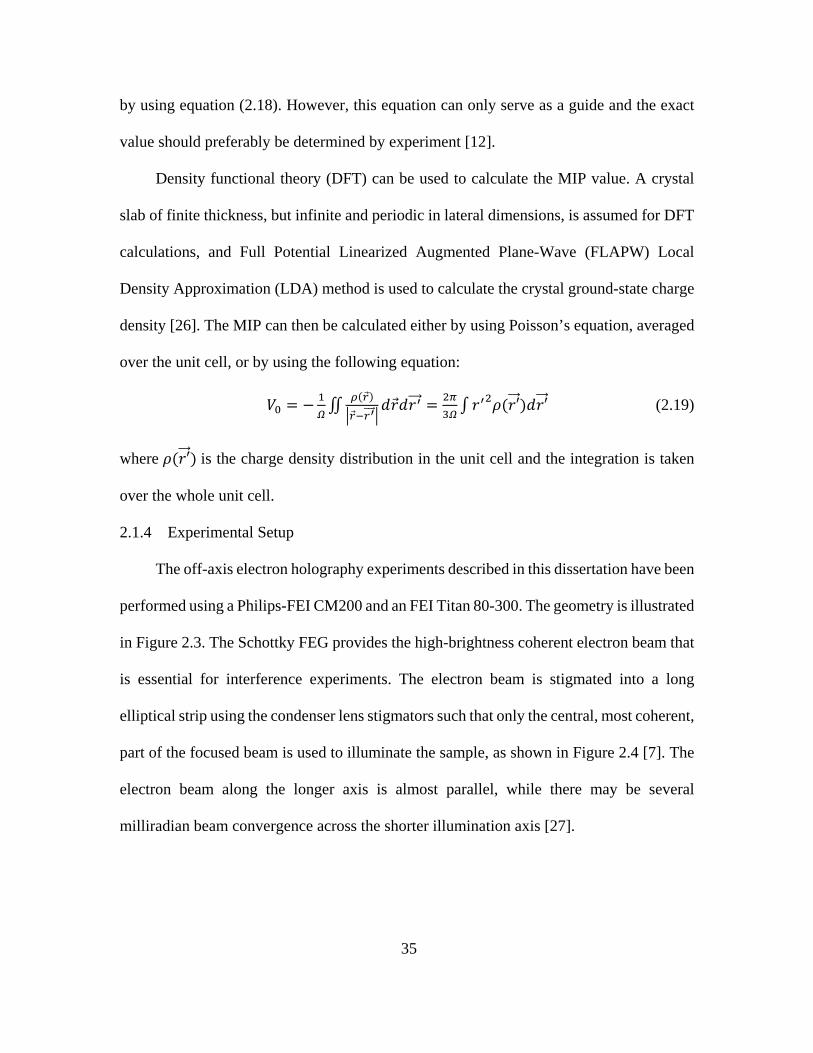
by using equation (2.18). However, this equation can only serve as a guide and the exact
value should preferably be determined by experiment [12].
Density functional theory (DFT) can be used to calculate the MIP value. A crystal
slab of finite thickness, but infinite and periodic in lateral dimensions, is assumed for DFT
calculations, and Full Potential Linearized Augmented Plane-Wave (FLAPW) Local
Density Approximation (LDA) method is used to calculate the crystal ground-state charge
density [26]. The MIP can then be calculated either by using Poisson’s equation, averaged
over the unit cell, or by using the following equation:
𝑉𝑉0 = − 1𝛺𝛺∬
𝜌𝜌(𝑟𝑟)
�𝑟𝑟−𝑟𝑟′����⃗ �𝑎𝑎𝑟𝑟𝑎𝑎𝑟𝑟′���⃗ = 2𝜋𝜋
3𝛺𝛺 ∫ 𝑟𝑟′2𝜌𝜌(𝑟𝑟′��⃗ )𝑎𝑎𝑟𝑟′��⃗ (2.19)
where 𝜌𝜌(𝑟𝑟′��⃗ ) is the charge density distribution in the unit cell and the integration is taken
over the whole unit cell.
2.1.4 Experimental Setup
The off-axis electron holography experiments described in this dissertation have been
performed using a Philips-FEI CM200 and an FEI Titan 80-300. The geometry is illustrated
in Figure 2.3. The Schottky FEG provides the high-brightness coherent electron beam that
is essential for interference experiments. The electron beam is stigmated into a long
elliptical strip using the condenser lens stigmators such that only the central, most coherent,
part of the focused beam is used to illuminate the sample, as shown in Figure 2.4 [7]. The
electron beam along the longer axis is almost parallel, while there may be several
milliradian beam convergence across the shorter illumination axis [27].
35
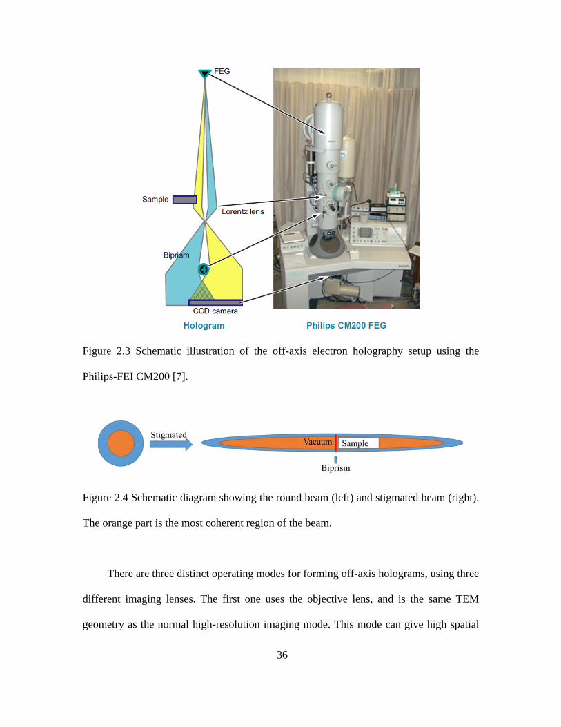
Figure 2.3 Schematic illustration of the off-axis electron holography setup using the
Philips-FEI CM200 [7].
Figure 2.4 Schematic diagram showing the round beam (left) and stigmated beam (right).
The orange part is the most coherent region of the beam.
There are three distinct operating modes for forming off-axis holograms, using three
different imaging lenses. The first one uses the objective lens, and is the same TEM
geometry as the normal high-resolution imaging mode. This mode can give high spatial
36
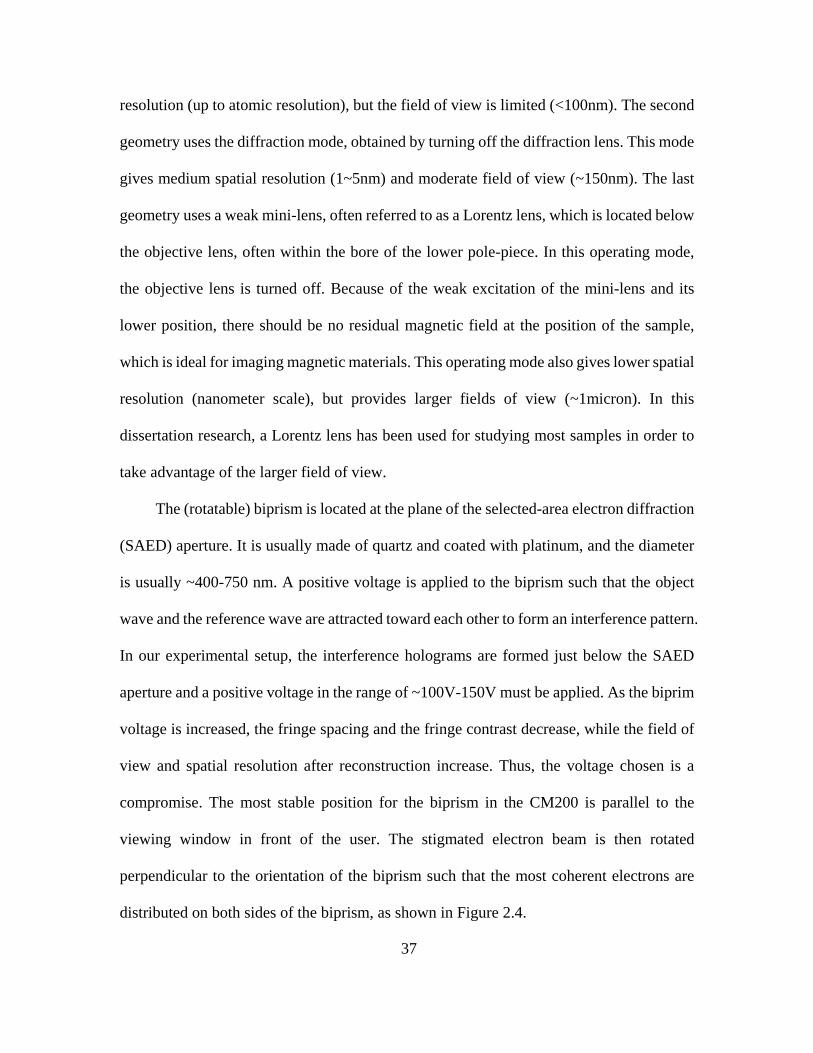
resolution (up to atomic resolution), but the field of view is limited (<100nm). The second
geometry uses the diffraction mode, obtained by turning off the diffraction lens. This mode
gives medium spatial resolution (1~5nm) and moderate field of view (~150nm). The last
geometry uses a weak mini-lens, often referred to as a Lorentz lens, which is located below
the objective lens, often within the bore of the lower pole-piece. In this operating mode,
the objective lens is turned off. Because of the weak excitation of the mini-lens and its
lower position, there should be no residual magnetic field at the position of the sample,
which is ideal for imaging magnetic materials. This operating mode also gives lower spatial
resolution (nanometer scale), but provides larger fields of view (~1micron). In this
dissertation research, a Lorentz lens has been used for studying most samples in order to
take advantage of the larger field of view.
The (rotatable) biprism is located at the plane of the selected-area electron diffraction
(SAED) aperture. It is usually made of quartz and coated with platinum, and the diameter
is usually ~400-750 nm. A positive voltage is applied to the biprism such that the object
wave and the reference wave are attracted toward each other to form an interference pattern.
In our experimental setup, the interference holograms are formed just below the SAED
aperture and a positive voltage in the range of ~100V-150V must be applied. As the biprim
voltage is increased, the fringe spacing and the fringe contrast decrease, while the field of
view and spatial resolution after reconstruction increase. Thus, the voltage chosen is a
compromise. The most stable position for the biprism in the CM200 is parallel to the
viewing window in front of the user. The stigmated electron beam is then rotated
perpendicular to the orientation of the biprism such that the most coherent electrons are
distributed on both sides of the biprism, as shown in Figure 2.4.
37
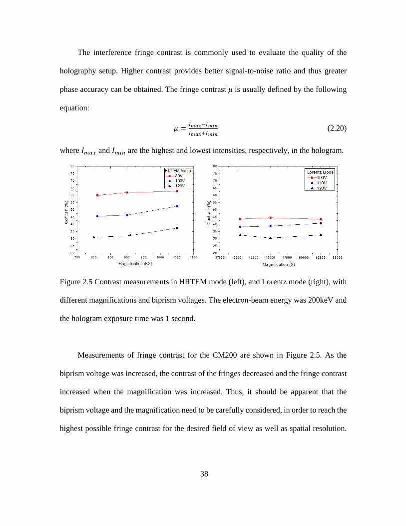
The interference fringe contrast is commonly used to evaluate the quality of the
holography setup. Higher contrast provides better signal-to-noise ratio and thus greater
phase accuracy can be obtained. The fringe contrast 𝜇𝜇 is usually defined by the following
equation:
𝜇𝜇 = 𝐼𝐼𝑠𝑠𝑎𝑎𝑚𝑚−𝐼𝐼𝑠𝑠𝑖𝑖𝑚𝑚𝐼𝐼𝑠𝑠𝑎𝑎𝑚𝑚+𝐼𝐼𝑠𝑠𝑖𝑖𝑚𝑚
(2.20)
where 𝐼𝐼𝑚𝑚𝑠𝑠𝑚𝑚 and 𝐼𝐼𝑚𝑚𝑖𝑖𝑛𝑛 are the highest and lowest intensities, respectively, in the hologram.
Figure 2.5 Contrast measurements in HRTEM mode (left), and Lorentz mode (right), with
different magnifications and biprism voltages. The electron-beam energy was 200keV and
the hologram exposure time was 1 second.
Measurements of fringe contrast for the CM200 are shown in Figure 2.5. As the
biprism voltage was increased, the contrast of the fringes decreased and the fringe contrast
increased when the magnification was increased. Thus, it should be apparent that the
biprism voltage and the magnification need to be carefully considered, in order to reach the
highest possible fringe contrast for the desired field of view as well as spatial resolution.
38
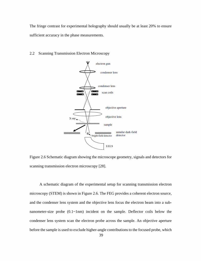
The fringe contrast for experimental holography should usually be at least 20% to ensure
sufficient accuracy in the phase measurements.
2.2 Scanning Transmission Electron Microscopy
Figure 2.6 Schematic diagram showing the microscope geometry, signals and detectors for
scanning transmission electron microscopy [28].
A schematic diagram of the experimental setup for scanning transmission electron
microscopy (STEM) is shown in Figure 2.6. The FEG provides a coherent electron source,
and the condenser lens system and the objective lens focus the electron beam into a sub-
nanometer-size probe (0.1~1nm) incident on the sample. Deflector coils below the
condenser lens system scan the electron probe across the sample. An objective aperture
before the sample is used to exclude higher-angle contributions to the focused probe, which 39
will otherwise lead to probe-blurring because of aberrations of the objective lens [28]. The
electron probe passes through the sample and electrons are scattered at different angles.
The STEM image is formed by successfully collecting electrons scattered at different probe
positions, and the magnification is determined by the area scanned on the sample relative
to the final monitor.
Four different types of signals can be collected after the electron-sample interactions
have taken place [28]: (a) Transmitted electrons that are scattered at low angles (smaller
than the incident-beam convergence angle). This signal represents the bright-field image.
(b) Electrons scattered at high angles (usually several times the incident beam convergence
angle). Annular-dark-field images are formed by collecting this signal. High-angle annular-
dark field (HAADF) imaging usually refers to collection angles of greater than ~50mrad,
and the signal intensity then depends on the sample atomic number Zα (α~1.5-2.0,
depending on the inner collection angle) [29]. (c) Transmitted electrons which have lost
energy due to electron-sample interactions, can be collected by an electron spectrometer.
This operation mode is referred to as electron-energy-loss spectroscopy (EELS). By
measuring the electron distribution as a function of energy loss, the elements in the sample,
bonding conditions and electron-sample interactions can be determined [15]. (d) X-rays
generated by electron excitations in the sample when atoms return to their ground state
after energy is absorbed from incident electrons. This mode is referred to as Energy-
dispersive X-ray spectroscopy (EDX) [30]. The EDX technique can be used to determine
elemental composition and distribution in the sample but no local bonding information is
available. In the research of this dissertation, HAADF, EDX and EELS have been used to
determine the structure and local composition in semiconductor nanowires (NWs).
40
2.3 Electron-Energy-Loss Spectroscopy
When the incident electron beam passes through the sample, coulombic interactions
between the electron beam and atoms in the sample cause inelastic scattering so that some
of the incident beam energy is lost to the sample. By analyzing the electron distribution in
the EELS spectrum as a function of energy, the excitation spectrum of the sample can be
extracted.
The EELS spectrum can be divided into three regions: zero-loss peak, low-loss region
and core-loss region. The zero-loss peak is caused primarily by the transmitted electrons
without any energy loss. For thin specimens, this peak is the most intense signal in the
EELS spectrum. The spatial resolution and contrast of images can be enhanced by using
this peak to filter out the inelastically scattered electrons [30]. The low-loss region is
usually in the range of ~5eV-50eV. This region is related to plasmon excitations, dielectric
properties, band gap, interband transitions and surface boundary effects, and is caused by
interactions of the fast electron beam with outer shell electrons near the Fermi level of the
material [28,30]. The combination of the zero-loss peak and the low-loss region can be also
used to estimate the local thickness of the sample t, as given by the following equation [31]:
𝐼𝐼0𝐼𝐼𝑡𝑡𝑜𝑜𝑡𝑡𝑎𝑎𝑡𝑡
= 𝑒𝑒− 𝑡𝑡𝜆𝜆𝑖𝑖 (2. 21)
where 𝐼𝐼0 is the intensity of the zero loss peak, 𝐼𝐼𝑡𝑡𝑜𝑜𝑡𝑡𝑠𝑠𝑜𝑜 is the total intensity including zero-
loss peak and low-loss region, and 𝜆𝜆𝑖𝑖 is the inelastic mean free path. The core-loss region
is usually in the energy range above 100eV, and is caused by inelastic interactions between
the electron beam and inner/core shell electrons of the material. When the inner-shell
electrons get enough energy from the electron beam, electrons transfer from the inner shells
41
to empty states and the atom is ionized. Therefore, the core-loss region is related to the
inner-shell electron orbits and can be used for elemental identification and quantification.
Moreover, the energy-loss near-edge structure (ELNES) within ~50eV of the ionization
energy is sensitive to local bonding and can often be used for identifying atom bonding
conditions in the material [28,30,31].
In general, EELS has higher energy resolution and better spatial resolution,
compared to EDX, which is a secondary effect of electron excitation caused by x ray
emission when electrons return to the ground state. The EELS technique is preferred for
light elements, while EDX is restricted by the fluorescence yield and absorption. However,
EELS cross-sections decrease rapidly for heavier elements, and the signal-to-noise ratio is
low, whereas EDX has strong signal-to-noise ratio. Therefore, EDX and EELS can be
considered as complementary [30]. The core-loss part of the EELS spectrum has been used
in this research to determine NW elemental distributions.
2.4 Sample Preparation
Proper sample preparation is essential for electron holography experiments because
of its impact on the phase measurements. In addition to electron transparency, large areas
of nearby vacuum are needed for the reference wave.
The NW samples have been prepared for observation using the following procedure:
(a) A small piece of substrate with upright NWs is cut off and put into isopropyl alcohol
(IPA). (b) The IPA with substrate is sonicated for 30s. The NWs are removed from the
substrate and float in the IPA solution. (c) The IPA solution with NWs is transferred to a
TEM grid with lacey carbon film or solid carbon thin film (thickness of several nanometers)
42
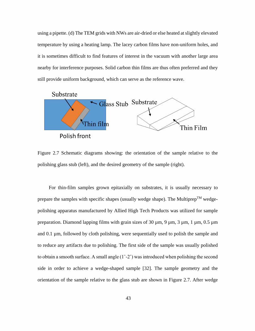
using a pipette. (d) The TEM grids with NWs are air-dried or else heated at slightly elevated
temperature by using a heating lamp. The lacey carbon films have non-uniform holes, and
it is sometimes difficult to find features of interest in the vacuum with another large area
nearby for interference purposes. Solid carbon thin films are thus often preferred and they
still provide uniform background, which can serve as the reference wave.
Figure 2.7 Schematic diagrams showing: the orientation of the sample relative to the
polishing glass stub (left), and the desired geometry of the sample (right).
For thin-film samples grown epitaxially on substrates, it is usually necessary to
prepare the samples with specific shapes (usually wedge shape). The MultiprepTM wedge-
polishing apparatus manufactured by Allied High Tech Products was utilized for sample
preparation. Diamond lapping films with grain sizes of 30 µm, 9 µm, 3 µm, 1 µm, 0.5 µm
and 0.1 µm, followed by cloth polishing, were sequentially used to polish the sample and
to reduce any artifacts due to polishing. The first side of the sample was usually polished
to obtain a smooth surface. A small angle (1˚-2˚) was introduced when polishing the second
side in order to achieve a wedge-shaped sample [32]. The sample geometry and the
orientation of the sample relative to the glass stub are shown in Figure 2.7. After wedge
43

polishing, the sample was typically ion-milled at 2keV for ~10 minutes to clean up any
debris remaining on the sample surface.
44
References
[1] M. R. McCartney, N. Agarwal, S. Chung, D. A. Cullen, M.-G. Han, K. He, L. Li, H. Wang, L. Zhou, and D. J. Smith, Ultramicroscopy 110 375 (2010).
[2] D. Gabor, Proceedings of the Royal Society of London. Series A. Mathematical and Physical Sciences 197 454 (1949).
[3] E. N. Leith and J. Upatnieks, J. Opt. Soc. Am. 52 1123 (1962).
[4] G. Möllenstedt and H. Wahl, Naturwissenschaften 55 340 (1968).
[5] A. V. Crewe and J. Wall, Journal of Molecular Biology 48 375 (1970).
[6] A. Tonomura, Reviews of Modern Physics 59 639 (1987).
[7] M. R. McCartney and D. J. Smith, Annual Review of Materials Research 37 729 (2007).
[8] J. M. Cowley, Ultramicroscopy 41 335 (1992).
[9] M. Lehmann and H. Lichte, Microscopy and Microanalysis 8 447 (2004).
[10] H. Lichte, P. Formanek, A. Lenk, M. Linck, C. Matzeck, M. Lehmann, and P. Simon, Annual Review of Materials Research 37 539 (2007).
[11] D. C. Ghiglia and M. D. Pritt, Two-dimensional phase unwrapping : theory, algorithms, and software. Wiley, New York, (1998).
[12] M. Gajdardziska-Josifovska and A. H. Carim, Chapter 12, Introduction to electron holography, Kluwer Academic/Plenum Publishers, New York, (1999).
[13] M. I. den Hertog, H. Schmid, D. Cooper, J. L. Rouviere, M. T. Bjork, H. Riel, P. Rivallin, S. Karg, and W. Riess, Nano letters 9 3837 (2009).
[14] M. R. McCartney and M. Gajdardziska-Josifovska, Ultramicroscopy 53 283 (1994).
[15] R. F. Egerton, Electron energy-loss spectroscopy in the electron microscope, 2nd ed. Plenum Press, New York, (1996).
[16] J. Spence, Acta Crystallographica Section A 49 231 (1993).
[17] J. C. H. Spence and J. M. Zuo, Electron microdiffraction. Plenum Press, New York, (1992).
[18] P. Becker and P. Coppens, Acta Crystallographica Section A 46 254 (1990).
45
[19] S. Miyake, Proc. Phys. Math. Soc. Japan 22 666 (1940).
[20] J. Ibers, Acta Crystallographica 11 178 (1958).
[21] L. Reimer, Transmission electron microscopy : physics of image formation and microanalysis, 4th ed. Springer, New York, (1997).
[22] P. A. Doyle and P. S. Turner, Acta Crystallographica Section A 24 390 (1968).
[23] G. Radi, Acta Crystallographica Section A 26 41 (1970).
[24] H. Bethe, Ann. Phys. 87 55 (1928).
[25] F. M. Ross and W. M. Stobbs, Philosophical Magazine A 63 37 (1991).
[26] M. Y. Kim, J. M. Zuo, and J. C. H. Spence, physica status solidi (a) 166 445 (1998).
[27] M. Lehmann, Ultramicroscopy 100 9 (2004).
[28] S. J. Pennycook, P. D. Nellist, Scanning Transmission Electron Microscopy Imaging and Analysis. Springer, New York, NY, (2011).
[29] P. Hartel, H. Rose, and C. Dinges, Ultramicroscopy 63 93 (1996).
[30] D. B. Williams and C. B. Carter, Transmission electron microscopy : a textbook for materials science, 2nd ed. Springer, New York, (2009).
[31] C. C. Ahn, Transmission electron energy loss spectrometry in materials science and the EELS atlas, 2nd ed. Wiley, Weinheim, Germany, (2004).
[32] MultiPrepTM operating manual of Allied High Tech Products, Inc.
46
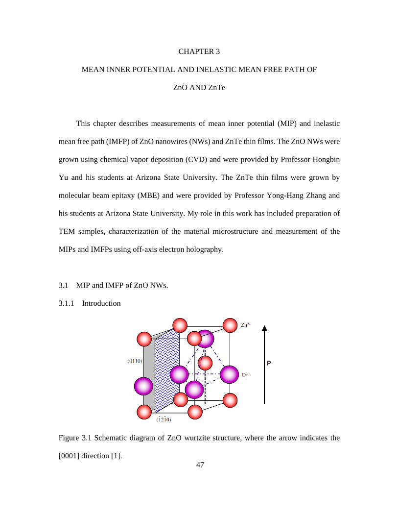
CHAPTER 3
MEAN INNER POTENTIAL AND INELASTIC MEAN FREE PATH OF
ZnO AND ZnTe
This chapter describes measurements of mean inner potential (MIP) and inelastic
mean free path (IMFP) of ZnO nanowires (NWs) and ZnTe thin films. The ZnO NWs were
grown using chemical vapor deposition (CVD) and were provided by Professor Hongbin
Yu and his students at Arizona State University. The ZnTe thin films were grown by
molecular beam epitaxy (MBE) and were provided by Professor Yong-Hang Zhang and
his students at Arizona State University. My role in this work has included preparation of
TEM samples, characterization of the material microstructure and measurement of the
MIPs and IMFPs using off-axis electron holography.
3.1 MIP and IMFP of ZnO NWs.
3.1.1 Introduction
Figure 3.1 Schematic diagram of ZnO wurtzite structure, where the arrow indicates the
[0001] direction [1]. 47
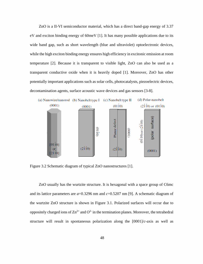
ZnO is a II-VI semiconductor material, which has a direct band-gap energy of 3.37
eV and exciton binding energy of 60meV [1]. It has many possible applications due to its
wide band gap, such as short wavelength (blue and ultraviolet) optoelectronic devices,
while the high exciton binding energy ensures high efficiency in excitonic emission at room
temperature [2]. Because it is transparent to visible light, ZnO can also be used as a
transparent conductive oxide when it is heavily doped [1]. Moreover, ZnO has other
potentially important applications such as solar cells, photocatalysts, piezoelectric devices,
decontamination agents, surface acoustic wave devices and gas sensors [3-8].
Figure 3.2 Schematic diagram of typical ZnO nanostructures [1].
ZnO usually has the wurtzite structure. It is hexagonal with a space group of C6mc
and its lattice parameters are a=0.3296 nm and c=0.5207 nm [9]. A schematic diagram of
the wurtzite ZnO structure is shown in Figure 3.1. Polarized surfaces will occur due to
oppositely charged ions of Zn2+ and O2- in the termination planes. Moreover, the tetrahedral
structure will result in spontaneous polarization along the [0001]/c-axis as well as
48
piezoelectricity and pyroelectricity because of non-centrosymmetry [1]. The common
directions for fast growth of ZnO include [2͞1͞10], [01͞10] and ±[0001].
Typical ZnO nanostructures are illustrated in Figure 3.2 [1]. Different ZnO
nanostructures have been achieved, such as nanowires (NWs), nanorods, nanotubes,
nanobelts, nano-sheets, and nanostars [2,10-19]. Among these, the ZnO NWs and nano-
sheets have received much interest because they have one/two dimensional structures, large
surface-to-volume ratio and quantum confinement effects, which enable novel physical
properties and applications [1,20]. Understanding the MIP and IMFP of ZnO is very
important for further thickness and built-in potential measurements of ZnO nanostructures
and semiconductors using off-axis electron holography [21]. In this research, conventional
TEM was used to study the morphology of the ZnO NWs. Off-axis electron holography
was then used to determine the MIP and IMFP of ZnO using ZnO NWs. Thickness
measurements of ZnO thin sheets were performed using the measured MIP and IMFP
values.
3.1.2 Experimental Details and Results
Samples for TEM characterization were prepared by sonicating the substrate with
vertical ZnO NWs in isopropyl alcohol solution to dislodge NWs, followed by transferring
the solution to TEM grids with lacey carbon supports using pipettes and then air-dried. Off-
axis electron holography observations were done using the Philips-FEI CM200 operated at
200kV. In order to obtain larger fields of view, the normal objective lens was turned off,
and the Lorentz mini-lens was used for imaging. The typical biprism voltage was 120V
giving interference-fringe spacings of ~5 nm and the exposure time for hologram recording
was normally 1 second.
49
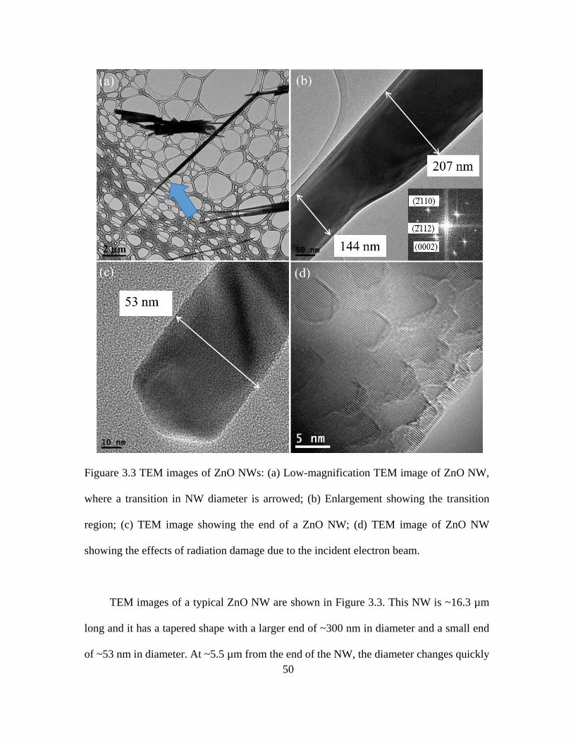
Figuare 3.3 TEM images of ZnO NWs: (a) Low-magnification TEM image of ZnO NW,
where a transition in NW diameter is arrowed; (b) Enlargement showing the transition
region; (c) TEM image showing the end of a ZnO NW; (d) TEM image of ZnO NW
showing the effects of radiation damage due to the incident electron beam.
TEM images of a typical ZnO NW are shown in Figure 3.3. This NW is ~16.3 µm
long and it has a tapered shape with a larger end of ~300 nm in diameter and a small end
of ~53 nm in diameter. At ~5.5 µm from the end of the NW, the diameter changes quickly 50
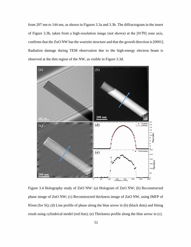
from 207 nm to 144 nm, as shown in Figures 3.3a and 3.3b. The diffractogram in the insert
of Figure 3.3b, taken from a high-resolution image (not shown) at the [01͞10] zone axis,
confirms that the ZnO NW has the wurtzite structure and that the growth direction is [0001].
Radiation damage during TEM observation due to the high-energy electron beam is
observed at the thin region of the NW, as visible in Figure 3.3d.
Figure 3.4 Holography study of ZnO NW: (a) Hologram of ZnO NW; (b) Reconstructed
phase image of ZnO NW; (c) Reconstructed thickness image of ZnO NW, using IMFP of
85nm (for Si); (d) Line profile of phase along the blue arrow in (b) (black dots) and fitting
result using cylindrical model (red line); (e) Thickness profile along the blue arrow in (c).
51
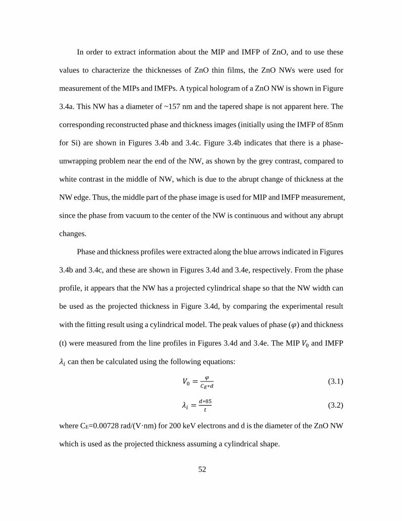
In order to extract information about the MIP and IMFP of ZnO, and to use these
values to characterize the thicknesses of ZnO thin films, the ZnO NWs were used for
measurement of the MIPs and IMFPs. A typical hologram of a ZnO NW is shown in Figure
3.4a. This NW has a diameter of ~157 nm and the tapered shape is not apparent here. The
corresponding reconstructed phase and thickness images (initially using the IMFP of 85nm
for Si) are shown in Figures 3.4b and 3.4c. Figure 3.4b indicates that there is a phase-
unwrapping problem near the end of the NW, as shown by the grey contrast, compared to
white contrast in the middle of NW, which is due to the abrupt change of thickness at the
NW edge. Thus, the middle part of the phase image is used for MIP and IMFP measurement,
since the phase from vacuum to the center of the NW is continuous and without any abrupt
changes.
Phase and thickness profiles were extracted along the blue arrows indicated in Figures
3.4b and 3.4c, and these are shown in Figures 3.4d and 3.4e, respectively. From the phase
profile, it appears that the NW has a projected cylindrical shape so that the NW width can
be used as the projected thickness in Figure 3.4d, by comparing the experimental result
with the fitting result using a cylindrical model. The peak values of phase (𝑖𝑖) and thickness
(t) were measured from the line profiles in Figures 3.4d and 3.4e. The MIP 𝑉𝑉0 and IMFP
𝜆𝜆𝑖𝑖 can then be calculated using the following equations:
𝑉𝑉0 = 𝜑𝜑𝐶𝐶𝐸𝐸∗𝑅𝑅
(3.1)
𝜆𝜆𝑖𝑖 = 𝑅𝑅∗85𝑡𝑡
(3.2)
where CE=0.00728 rad/(V·nm) for 200 keV electrons and d is the diameter of the ZnO NW
which is used as the projected thickness assuming a cylindrical shape.
52
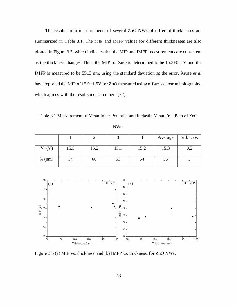
The results from measurements of several ZnO NWs of different thicknesses are
summarized in Table 3.1. The MIP and IMFP values for different thicknesses are also
plotted in Figure 3.5, which indicates that the MIP and IMFP measurements are consistent
as the thickness changes. Thus, the MIP for ZnO is determined to be 15.3±0.2 V and the
IMFP is measured to be 55±3 nm, using the standard deviation as the error. Kruse et al
have reported the MIP of 15.9±1.5V for ZnO measured using off-axis electron holography,
which agrees with the results measured here [22].
Table 3.1 Measurement of Mean Inner Potential and Inelastic Mean Free Path of ZnO
NWs.
1 2 3 4 Average Std. Dev.
V0 (V) 15.5 15.2 15.1 15.2 15.3 0.2
λi (nm) 54 60 53 54 55 3
Figure 3.5 (a) MIP vs. thickness, and (b) IMFP vs. thickness, for ZnO NWs.
53
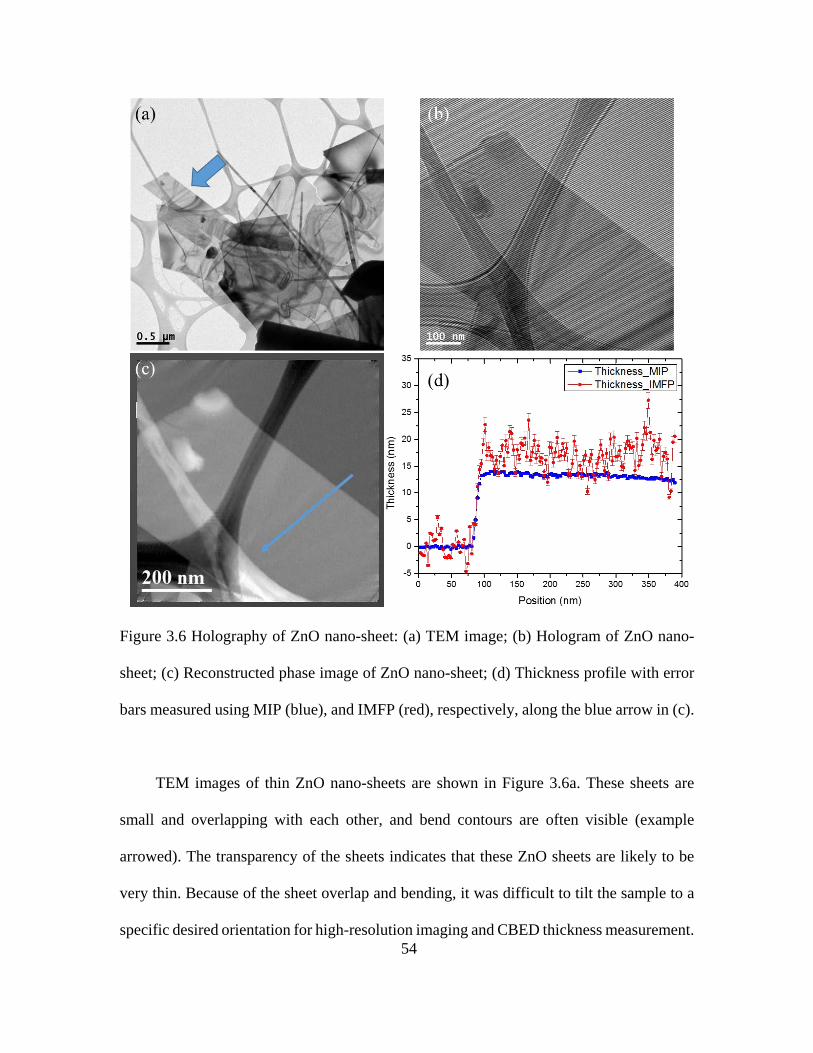
Figure 3.6 Holography of ZnO nano-sheet: (a) TEM image; (b) Hologram of ZnO nano-
sheet; (c) Reconstructed phase image of ZnO nano-sheet; (d) Thickness profile with error
bars measured using MIP (blue), and IMFP (red), respectively, along the blue arrow in (c).
TEM images of thin ZnO nano-sheets are shown in Figure 3.6a. These sheets are
small and overlapping with each other, and bend contours are often visible (example
arrowed). The transparency of the sheets indicates that these ZnO sheets are likely to be
very thin. Because of the sheet overlap and bending, it was difficult to tilt the sample to a
specific desired orientation for high-resolution imaging and CBED thickness measurement. 54
The sample was tilted to avoid diffraction contrast, and off-axis electron holography was
instead used to measure the sheet thickness. The blue arrow in Figure 3.6a indicates the
thin sheet used for the holography experiment.
The hologram of the ZnO nano-sheet and its reconstructed phase image are shown in
Figures 3.6b and 3.6c, respectively. The thickness image (not shown) was calculated from
the reconstructed amplitude image (not shown), using the IMFP of 55 nm obtained from
the ZnO NW measurements. The bend contours near the blue arrow in Figure 3.6a are
visible in the hologram (black contrast) as well as the phase image (white contrast), and
could introduce some diffraction contribution to the reconstructed phase and thickness
images. Thus, the phase and thickness profiles were extracted from the phase image and
thickness images, respectively, along the blue arrow in Figure 3.6c, where the bend contrast
is minimal. The thickness profiles of the ZnO nano-sheet along the blue arrow in Figure
3.6c, as calculated from the phase profile (blue line), and from the thickness profile (red
line), respectively, are shown in Figure 3.6d. The thickness profile calculated using the
IMFP tends to be noisier, compared to the one calculated using the MIP, because the
thickness image is measured from the image intensity, whereas the phase image is
measured from the shift of interference fringes and the intensity might be influenced by
other effects, such as Fresnel fringes as well as uniformity and stability of beam intensity.
The thickness profile extracted from the thickness image gives a thickness of
~18±3nm, as measured from the region of 125nm-175nm in Figure 3.6d, and using the
combination of the standard deviation (2nm) in this region and the 6% error in λi
measurement (1nm) as the thickness measurement error.
55
An alternative approach for thickness measurement is to use the phase profile
extracted from the reconstructed phase image and the MIP value of 15.3 V obtained from
the ZnO NW measurement, using the equation:
𝑎𝑎 = 𝜑𝜑𝐶𝐶𝐸𝐸∗𝑉𝑉0
(3.3)
where CE=0.00728 rad/(V∙nm) for 200keV electrons, φ is the phase and V0 is the MIP.
Using the MIP approach gives the ZnO sheet thickness of ~14±1nm, as measured
over the range of 125nm-175nm in Figure 3.6d and using the combination of the standard
deviation (0.3nm) in this region and 2% error in V0 measurement (0.3nm) as the thickness
measurement error. In contrast, the IMFP method gave a value of ~18±3nm. Thus, the two
methods give consistent results. The 4nm difference between the MIP and IMFP
measurements reflect some of the inherent inaccuracies in the MIP and IMFP
measurements using ZnO NWs, which includes an assumption of cylindrical shape NWs,
limited MIP and IMFP measurement points, possible diffraction contrast and limited
spatial resolution in the reconstructed image (~4nm). More MIP and IMFP measurements
could reduce this inaccuracy. It is also possible that diffraction contrast is affecting the
thickness measurement because the nano-sheet orientation was changing during
observation.
3.1.3 Conclusions
Using off-axis electron holography and ZnO NWs, the MIP of ZnO was measured to
be 15.3±0.2 V, and the IMFP at 200keV was measured to be 55±3 nm. The MIP and IMFP
values were then used to characterize the thickness of a ZnO nano-sheet and gave consistent
results for thickness measurement in the range of 14nm-18nm. With knowledge of the MIP
and IMFP, it should become possible to extract the built-in potential in doped ZnO 56
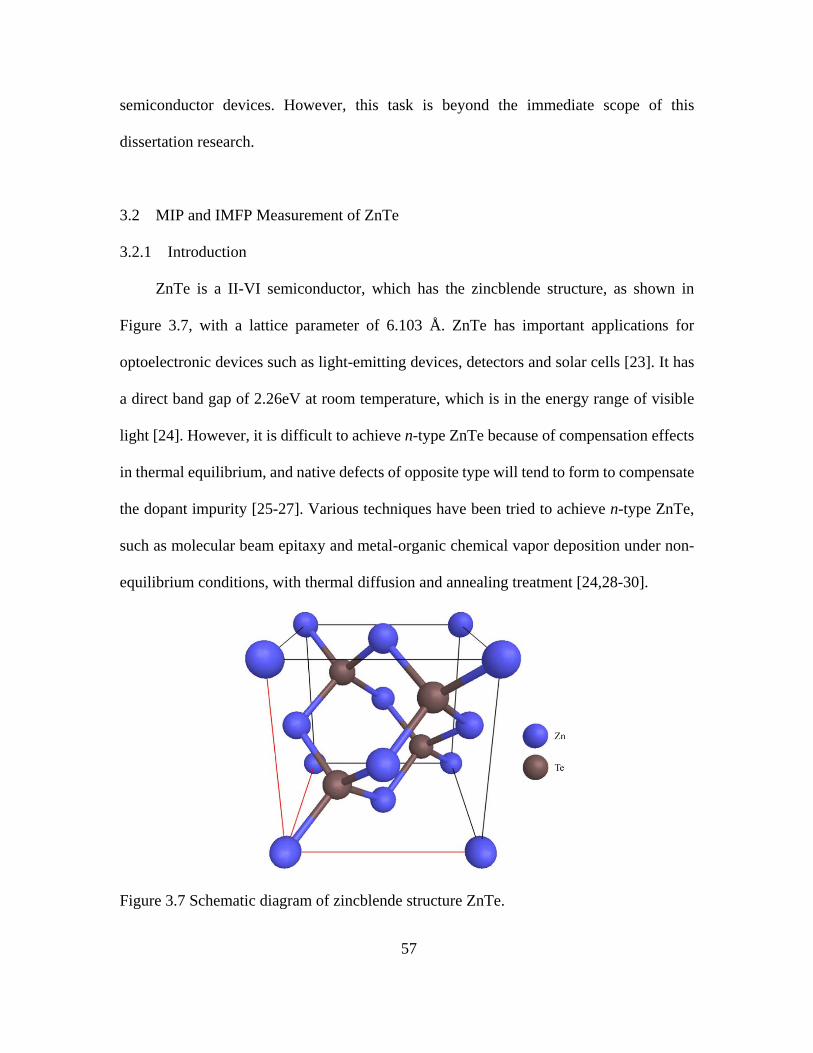
semiconductor devices. However, this task is beyond the immediate scope of this
dissertation research.
3.2 MIP and IMFP Measurement of ZnTe
3.2.1 Introduction
ZnTe is a II-VI semiconductor, which has the zincblende structure, as shown in
Figure 3.7, with a lattice parameter of 6.103 Å. ZnTe has important applications for
optoelectronic devices such as light-emitting devices, detectors and solar cells [23]. It has
a direct band gap of 2.26eV at room temperature, which is in the energy range of visible
light [24]. However, it is difficult to achieve n-type ZnTe because of compensation effects
in thermal equilibrium, and native defects of opposite type will tend to form to compensate
the dopant impurity [25-27]. Various techniques have been tried to achieve n-type ZnTe,
such as molecular beam epitaxy and metal-organic chemical vapor deposition under non-
equilibrium conditions, with thermal diffusion and annealing treatment [24,28-30].
Figure 3.7 Schematic diagram of zincblende structure ZnTe.
57
In order to improve device performance, it is desirable to understand the electrostatic
properties, such as the built-in potential and active dopant concentrations. However, it is
first necessary to determine the MIP and IMFP of ZnTe in order to extract the built-in
potential information using electron holography. In this research, off-axis electron
holography was used to determine the MIP and IMFP of ZnTe thin films.
3.2.2 Experiment Details and Results
Samples for TEM characterization were prepared using the Multi PrepTM wedge
polisher. A wedge-shaped sample was achieved by mechanical polishing, followed by a
brief period of argon-ion-milling to clean residue from the sample surface. Off-axis
electron holography observations were done using the Philips-FEI CM200 operated at
200kV. In order to obtain a larger field of view, the normal objective lens was turned off,
and the Lorentz mini-lens was used for imaging. The typical biprism voltage was 120V
and the exposure time for hologram recording was 1 second. The technique of convergent
beam electron diffraction (CBED) was used to determine the local sample thickness using
comparison with image simulations. The Bloch wave method was used to simulate
dynamic effects that could impact the phase measurements [31].
The intrinsic ZnTe sample was tilted to the [100] zone axis and CBED patterns were
recorded at different positions in the normal imaging mode. Beam damage as well as beam-
induced carbon contamination were caused by the high-energy electrons. These beam-
damaged regions with carbon contamination were later used was position markers for the
holography experiments. After the CBED observations, the sample was tilted slightly off
the zone axis to minimize diffraction contrast. The objective lens was then switched off
and the Lorentz mini-lens was used to obtain larger fields of view. Holograms were taken
58
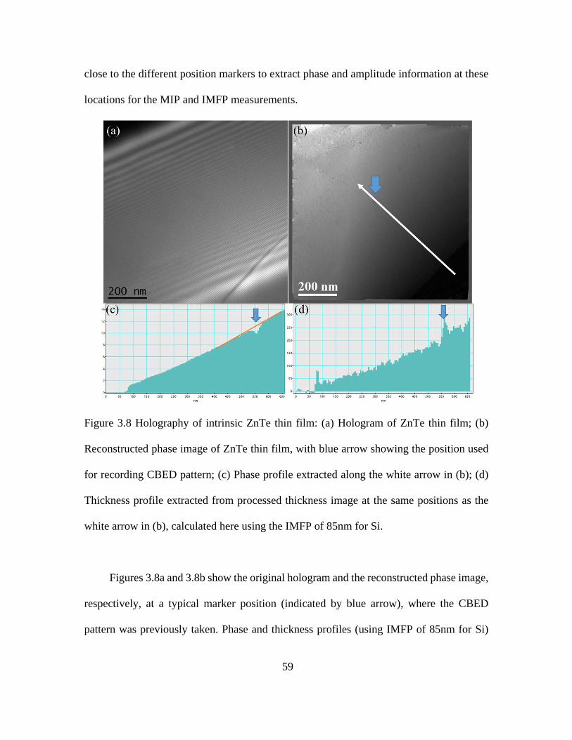
close to the different position markers to extract phase and amplitude information at these
locations for the MIP and IMFP measurements.
Figure 3.8 Holography of intrinsic ZnTe thin film: (a) Hologram of ZnTe thin film; (b)
Reconstructed phase image of ZnTe thin film, with blue arrow showing the position used
for recording CBED pattern; (c) Phase profile extracted along the white arrow in (b); (d)
Thickness profile extracted from processed thickness image at the same positions as the
white arrow in (b), calculated here using the IMFP of 85nm for Si.
Figures 3.8a and 3.8b show the original hologram and the reconstructed phase image,
respectively, at a typical marker position (indicated by blue arrow), where the CBED
pattern was previously taken. Phase and thickness profiles (using IMFP of 85nm for Si)
59
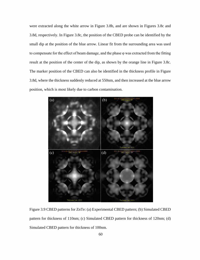
were extracted along the white arrow in Figure 3.8b, and are shown in Figures 3.8c and
3.8d, respectively. In Figure 3.8c, the position of the CBED probe can be identified by the
small dip at the position of the blue arrow. Linear fit from the surrounding area was used
to compensate for the effect of beam damage, and the phase φ was extracted from the fitting
result at the position of the center of the dip, as shown by the orange line in Figure 3.8c.
The marker position of the CBED can also be identified in the thickness profile in Figure
3.8d, where the thickness suddenly reduced at 550nm, and then increased at the blue arrow
position, which is most likely due to carbon contamination.
Figure 3.9 CBED patterns for ZnTe: (a) Experimental CBED pattern; (b) Simulated CBED
pattern for thickness of 110nm; (c) Simulated CBED pattern for thickness of 120nm; (d)
Simulated CBED pattern for thickness of 100nm.
60
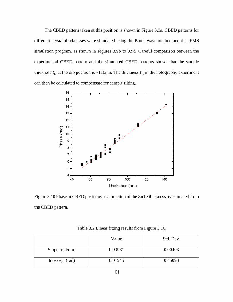
The CBED pattern taken at this position is shown in Figure 3.9a. CBED patterns for
different crystal thicknesses were simulated using the Bloch wave method and the JEMS
simulation program, as shown in Figures 3.9b to 3.9d. Careful comparison between the
experimental CBED pattern and the simulated CBED patterns shows that the sample
thickness 𝑎𝑎𝐶𝐶 at the dip position is ~110nm. The thickness 𝑎𝑎ℎ in the holography experiment
can then be calculated to compensate for sample tilting.
Figure 3.10 Phase at CBED positions as a function of the ZnTe thickness as estimated from
the CBED pattern.
Table 3.2 Linear fitting results from Figure 3.10.
Value Std. Dev.
Slope (rad/nm) 0.09981 0.00403
Intercept (rad) 0.01945 0.45093
61
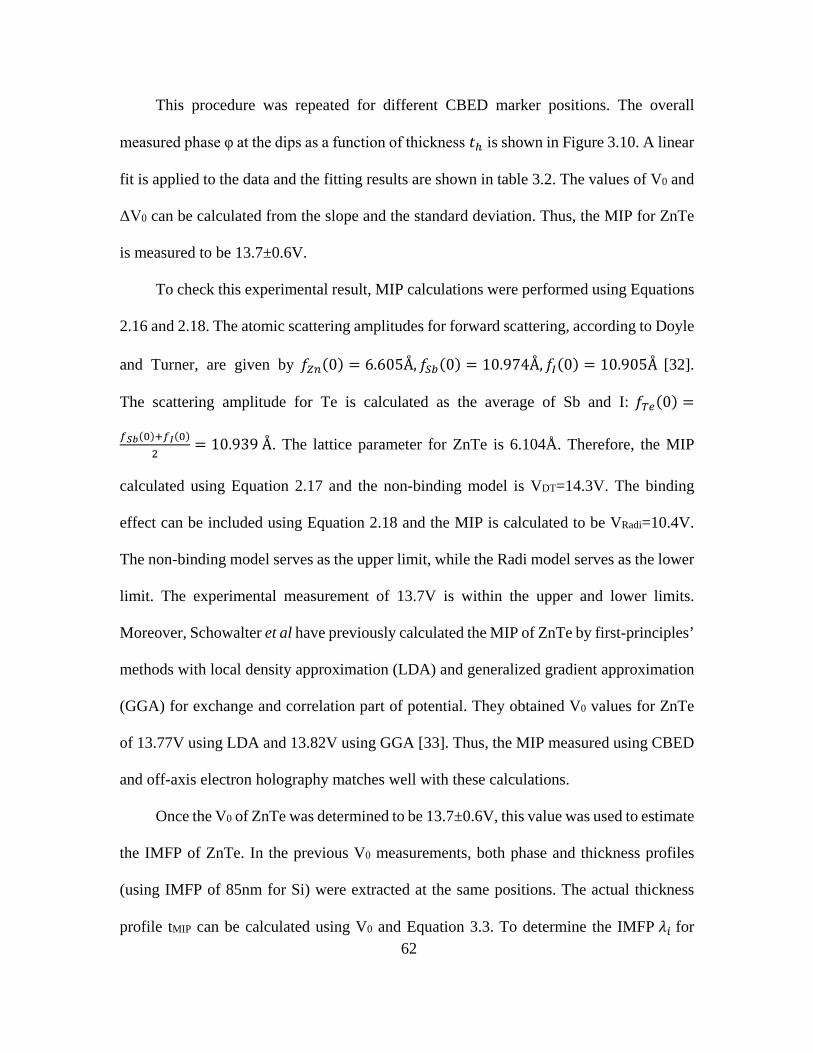
This procedure was repeated for different CBED marker positions. The overall
measured phase φ at the dips as a function of thickness 𝑎𝑎ℎ is shown in Figure 3.10. A linear
fit is applied to the data and the fitting results are shown in table 3.2. The values of V0 and
ΔV0 can be calculated from the slope and the standard deviation. Thus, the MIP for ZnTe
is measured to be 13.7±0.6V.
To check this experimental result, MIP calculations were performed using Equations
2.16 and 2.18. The atomic scattering amplitudes for forward scattering, according to Doyle
and Turner, are given by 𝑓𝑓𝑍𝑍𝑛𝑛(0) = 6.605Å,𝑓𝑓𝑆𝑆𝑏𝑏(0) = 10.974Å,𝑓𝑓𝐼𝐼(0) = 10.905Å [32].
The scattering amplitude for Te is calculated as the average of Sb and I: 𝑓𝑓𝑘𝑘𝑒𝑒(0) =
𝑟𝑟𝑆𝑆𝑏𝑏(0)+𝑟𝑟𝐼𝐼(0)2
= 10.939 Å. The lattice parameter for ZnTe is 6.104Å. Therefore, the MIP
calculated using Equation 2.17 and the non-binding model is VDT=14.3V. The binding
effect can be included using Equation 2.18 and the MIP is calculated to be VRadi=10.4V.
The non-binding model serves as the upper limit, while the Radi model serves as the lower
limit. The experimental measurement of 13.7V is within the upper and lower limits.
Moreover, Schowalter et al have previously calculated the MIP of ZnTe by first-principles’
methods with local density approximation (LDA) and generalized gradient approximation
(GGA) for exchange and correlation part of potential. They obtained V0 values for ZnTe
of 13.77V using LDA and 13.82V using GGA [33]. Thus, the MIP measured using CBED
and off-axis electron holography matches well with these calculations.
Once the V0 of ZnTe was determined to be 13.7±0.6V, this value was used to estimate
the IMFP of ZnTe. In the previous V0 measurements, both phase and thickness profiles
(using IMFP of 85nm for Si) were extracted at the same positions. The actual thickness
profile tMIP can be calculated using V0 and Equation 3.3. To determine the IMFP 𝜆𝜆𝑖𝑖 for 62
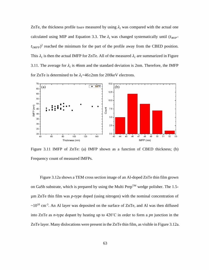
ZnTe, the thickness profile tIMFP measured by using 𝜆𝜆𝑖𝑖 was compared with the actual one
calculated using MIP and Equation 3.3. The 𝜆𝜆𝑖𝑖 was changed systematically until (𝑎𝑎𝑀𝑀𝐼𝐼𝑀𝑀-
𝑎𝑎𝐼𝐼𝑀𝑀𝐹𝐹𝑀𝑀)2 reached the minimum for the part of the profile away from the CBED position.
This 𝜆𝜆𝑖𝑖 is then the actual IMFP for ZnTe. All of the measured 𝜆𝜆𝑖𝑖 are summarized in Figure
3.11. The average for 𝜆𝜆𝑖𝑖 is 46nm and the standard deviation is 2nm. Therefore, the IMFP
for ZnTe is determined to be 𝜆𝜆𝑖𝑖=46±2nm for 200keV electrons.
Figure 3.11 IMFP of ZnTe: (a) IMFP shown as a function of CBED thickness; (b)
Frequency count of measured IMFPs.
Figure 3.12a shows a TEM cross section image of an Al-doped ZnTe thin film grown
on GaSb substrate, which is prepared by using the Multi PrepTM wedge polisher. The 1.5-
µm ZnTe thin film was p-type doped (using nitrogen) with the nominal concentration of
~1018 cm-3. An Al layer was deposited on the surface of ZnTe, and Al was then diffused
into ZnTe as n-type dopant by heating up to 420˚C in order to form a pn junction in the
ZnTe layer. Many dislocations were present in the ZnTe thin film, as visible in Figure 3.12a.
63
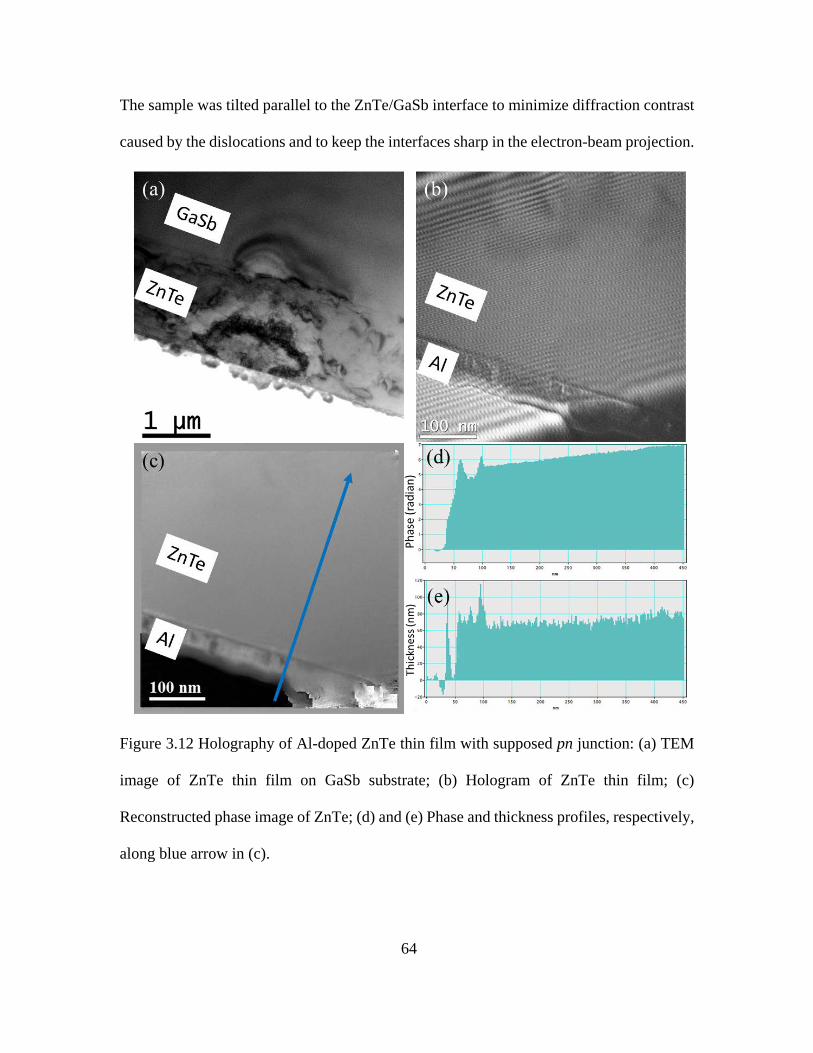
The sample was tilted parallel to the ZnTe/GaSb interface to minimize diffraction contrast
caused by the dislocations and to keep the interfaces sharp in the electron-beam projection.
Figure 3.12 Holography of Al-doped ZnTe thin film with supposed pn junction: (a) TEM
image of ZnTe thin film on GaSb substrate; (b) Hologram of ZnTe thin film; (c)
Reconstructed phase image of ZnTe; (d) and (e) Phase and thickness profiles, respectively,
along blue arrow in (c).
64
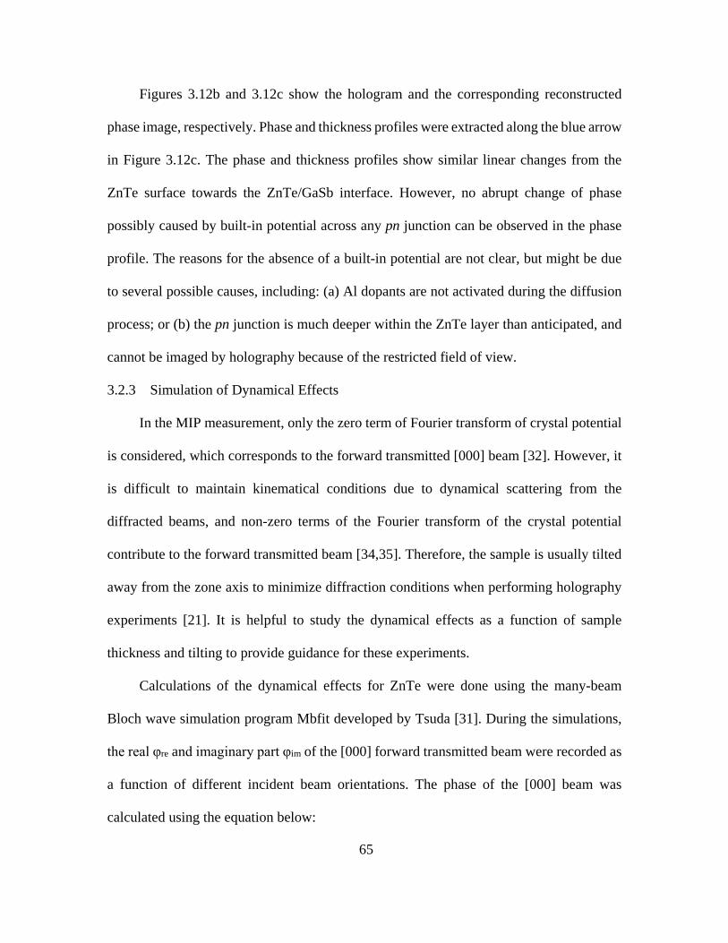
Figures 3.12b and 3.12c show the hologram and the corresponding reconstructed
phase image, respectively. Phase and thickness profiles were extracted along the blue arrow
in Figure 3.12c. The phase and thickness profiles show similar linear changes from the
ZnTe surface towards the ZnTe/GaSb interface. However, no abrupt change of phase
possibly caused by built-in potential across any pn junction can be observed in the phase
profile. The reasons for the absence of a built-in potential are not clear, but might be due
to several possible causes, including: (a) Al dopants are not activated during the diffusion
process; or (b) the pn junction is much deeper within the ZnTe layer than anticipated, and
cannot be imaged by holography because of the restricted field of view.
3.2.3 Simulation of Dynamical Effects
In the MIP measurement, only the zero term of Fourier transform of crystal potential
is considered, which corresponds to the forward transmitted [000] beam [32]. However, it
is difficult to maintain kinematical conditions due to dynamical scattering from the
diffracted beams, and non-zero terms of the Fourier transform of the crystal potential
contribute to the forward transmitted beam [34,35]. Therefore, the sample is usually tilted
away from the zone axis to minimize diffraction conditions when performing holography
experiments [21]. It is helpful to study the dynamical effects as a function of sample
thickness and tilting to provide guidance for these experiments.
Calculations of the dynamical effects for ZnTe were done using the many-beam
Bloch wave simulation program Mbfit developed by Tsuda [31]. During the simulations,
the real φre and imaginary part φim of the [000] forward transmitted beam were recorded as
a function of different incident beam orientations. The phase of the [000] beam was
calculated using the equation below:
65
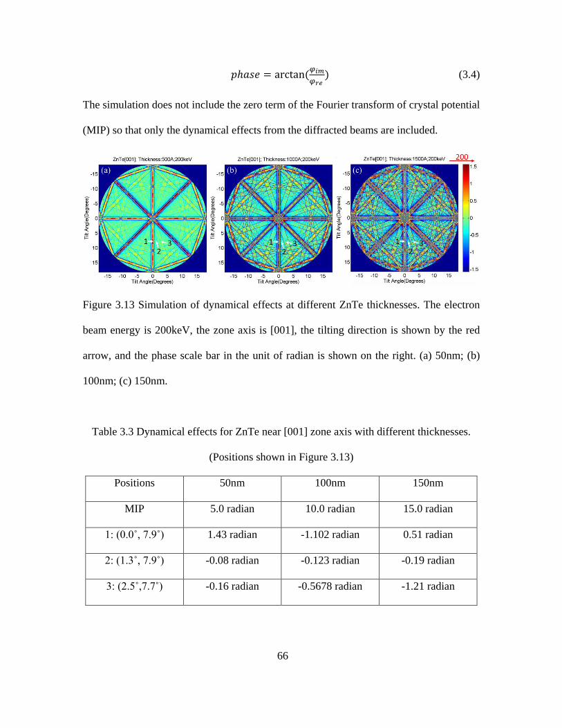
𝑝𝑝ℎ𝑎𝑎𝑎𝑎𝑒𝑒 = arctan (𝜑𝜑𝑖𝑖𝑠𝑠𝜑𝜑𝑟𝑟𝑟𝑟
) (3.4)
The simulation does not include the zero term of the Fourier transform of crystal potential
(MIP) so that only the dynamical effects from the diffracted beams are included.
Figure 3.13 Simulation of dynamical effects at different ZnTe thicknesses. The electron
beam energy is 200keV, the zone axis is [001], the tilting direction is shown by the red
arrow, and the phase scale bar in the unit of radian is shown on the right. (a) 50nm; (b)
100nm; (c) 150nm.
Table 3.3 Dynamical effects for ZnTe near [001] zone axis with different thicknesses.
(Positions shown in Figure 3.13)
Positions 50nm 100nm 150nm
MIP 5.0 radian 10.0 radian 15.0 radian
1: (0.0˚, 7.9˚) 1.43 radian -1.102 radian 0.51 radian
2: (1.3˚, 7.9˚) -0.08 radian -0.123 radian -0.19 radian
3: (2.5˚,7.7˚) -0.16 radian -0.5678 radian -1.21 radian
66
It is obvious and expected that the phase of the [000] beam changes as the direction
of the incident beam changes, as shown in Figure 3.13. To illustrate how the sample tilting
and thickness contribute to dynamical effects, three positions were chosen for each of the
thicknesses: (1) (0˚, 7.9˚) is in a major Kikuchi band, (2) (1.3˚, 7.9˚) is off the zone and
Kikuchi band and (3) (2.5˚, 7.7˚) is in a minor Kikuchi band. The results are shown in Table
3.3 and the phase shift solely due to MIP for 200keV electrons are also shown in the row
labeled MIP. When the beam is close to the zone axis or to Kikuchi bands, the dynamical
effects become more important, as shown at position (1), where the phase due to dynamical
effect fluctuates from 1.4 to 0.5 radian, as the thickness changes from 50 nm to 150 nm
and this effect is ~30% of the phase due to MIP at the thickness of 50nm. However, at
position (2), the phase only changes from -0.1 to -0.2 radian and its effect only takes ~2%.
Thus, it is usually necessary in holography experiments to tilt the sample away from the
zone axis and also to avoid major Kikuchi bands. The sample thickness increases from
Figure 3.13a to 3.13b and the dynamical effects become more obvious, by comparing the
results at position (3) for different thicknesses. Thus, the sample must be tilted to a low
diffraction contrast condition, when the sample is thick.
In Figure 3.14, the dynamical effects were simulated and compared for different zone
axes, while the other parameters were kept constant. These results indicate that the [111]
and [011] zone axes have more dynamical effects, compared to [001] axis. The area with
small phase change, such as in the range of -0.5 to 0.5 radian, is larger for the [001] zone
axis, compared to the other two cases. Choosing a low symmetry zone axis will obviously
reduce the diffraction scattering.
67
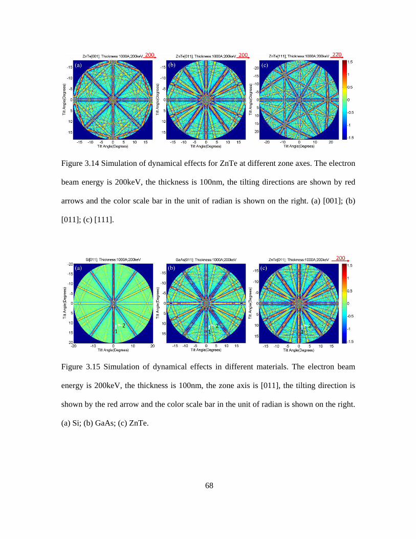
Figure 3.14 Simulation of dynamical effects for ZnTe at different zone axes. The electron
beam energy is 200keV, the thickness is 100nm, the tilting directions are shown by red
arrows and the color scale bar in the unit of radian is shown on the right. (a) [001]; (b)
[011]; (c) [111].
Figure 3.15 Simulation of dynamical effects in different materials. The electron beam
energy is 200keV, the thickness is 100nm, the zone axis is [011], the tilting direction is
shown by the red arrow and the color scale bar in the unit of radian is shown on the right.
(a) Si; (b) GaAs; (c) ZnTe.
68
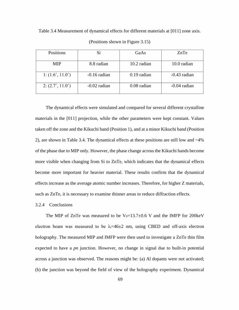
Table 3.4 Measurement of dynamical effects for different materials at [011] zone axis.
(Positions shown in Figure 3.15)
Positions Si GaAs ZnTe
MIP 8.8 radian 10.2 radian 10.0 radian
1: (1.6˚, 11.0˚) -0.16 radian 0.19 radian -0.43 radian
2: (2.7˚, 11.0˚) -0.02 radian 0.08 radian -0.04 radian
The dynamical effects were simulated and compared for several different crystalline
materials in the [011] projection, while the other parameters were kept constant. Values
taken off the zone and the Kikuchi band (Position 1), and at a minor Kikuchi band (Position
2), are shown in Table 3.4. The dynamical effects at these positions are still low and ~4%
of the phase due to MIP only. However, the phase change across the Kikuchi bands become
more visible when changing from Si to ZnTe, which indicates that the dynamical effects
become more important for heavier material. These results confirm that the dynamical
effects increase as the average atomic number increases. Therefore, for higher Z materials,
such as ZnTe, it is necessary to examine thinner areas to reduce diffraction effects.
3.2.4 Conclusions
The MIP of ZnTe was measured to be V0=13.7±0.6 V and the IMFP for 200keV
electron beam was measured to be λi=46±2 nm, using CBED and off-axis electron
holography. The measured MIP and IMFP were then used to investigate a ZnTe thin film
expected to have a pn junction. However, no change in signal due to built-in potential
across a junction was observed. The reasons might be: (a) Al dopants were not activated;
(b) the junction was beyond the field of view of the holography experiment. Dynamical
69

effects were systematically studied by using Bloch wave simulations. Choosing thinner
samples, avoiding low-index zone axes and careful tilting will all help to minimize
dynamical effects.
70
References
[1] Z. L. Wang, Journal of Physics: Condensed Matter 16 R829 (2004).
[2] M. H. Huang, S. Mao, H. Feick, H. Yan, Y. Wu, H. Kind, E. Weber, R. Russo, and P. Yang, Science 292 1897 (2001).
[3] B. Pal and M. Sharon, Mater Chem Phys 76 82 (2002).
[4] C. J. Lee, T. J. Lee, S. C. Lyu, Y. Zhang, H. Ruh, and H. J. Lee, Applied Physics Letters 81 3648 (2002).
[5] N. Ohashi, K. Kataoka, T. Ohgaki, T. Miyagi, H. Haneda, and K. Morinaga, Applied Physics Letters 83 4857 (2003).
[6] G. Sberveglieri, S. Groppelli, P. Nelli, A. Tintinelli, and G. Giunta, Sensors and Actuators B: Chemical 25 588 (1995).
[7] S. Baosheng, Y. Akira, and K. Makoto, Japanese Journal of Applied Physics 37 L206 (1998).
[8] J. J. Lee, Y. B. Kim, and Y. S. Yoon, Applied Surface Science 244 365 (2005).
[9] U. Özgür, Y. I. Alivov, C. Liu, A. Teke, M. A. Reshchikov, S. Doğan, V. Avrutin, S. J. Cho, and H. Morkoç, Journal of Applied Physics 98 041301 (2005).
[10] Y. Li, G. W. Meng, L. D. Zhang, and F. Phillipp, Applied Physics Letters 76 2011 (2000).
[11] Y. C. Kong, D. P. Yu, B. Zhang, W. Fang, and S. Q. Feng, Applied Physics Letters 78 407 (2001).
[12] J.-J. Wu, S.-C. Liu, C.-T. Wu, K.-H. Chen, and L.-C. Chen, Applied Physics Letters 81 1312 (2002).
[13] Z. W. Pan, Z. R. Dai, and Z. L. Wang, Science 291 1947 (2001).
[14] X. Y. Kong, Y. Ding, R. Yang, and Z. L. Wang, Science 303 1348 (2004).
[15] A. Sekar, S. H. Kim, A. Umar, and Y. B. Hahn, Journal of Crystal Growth 277 471 (2005).
[16] A. Umar, S. H. Kim, Y. S. Lee, K. S. Nahm, and Y. B. Hahn, Journal of Crystal Growth 282 131 (2005).
[17] B. P. Zhang, N. T. Binh, K. Wakatsuki, Y. Segawa, Y. Yamada, N. Usami, M. Kawasaki, and H. Koinuma, Applied Physics Letters 84 4098 (2004).
71
[18] A. Umar, S. Lee, Y. S. Lee, K. S. Nahm, and Y. B. Hahn, Journal of Crystal Growth 277 479 (2005).
[19] J. Q. Hu, Y. Bando, J. H. Zhan, Y. B. Li, and T. Sekiguchi, Applied Physics Letters 83 4414 (2003).
[20] A. Umar and Y. B. Hahn, Nanotechnology 17 2174 (2006).
[21] M. R. McCartney, N. Agarwal, S. Chung, D. A. Cullen, M.-G. Han, K. He, L. Li, H. Wang, L. Zhou, and D. J. Smith, Ultramicroscopy 110 375 (2010).
[22] E. Müller, P. Kruse, D. Gerthsen, M. Schowalter, A. Rosenauer, D. Lamoen, R. Kling, and A. Waag, Applied Physics Letters 86 154108 (2005).
[23] T. Tanaka, Q. Guo, M. Nishio, and H. Ogawa, Journal of Physics: Conference Series 61 1162 (2007).
[24] K. Sato, M. Hanafusa, A. Noda, A. Arakawa, M. Uchida, T. Asahi, and O. Oda, Journal of Crystal Growth 214–215 1080 (2000).
[25] G. Mandel, Physical Review 134 A1073 (1964).
[26] T. Teiji, M. Toyosaka, and T. Kiyoshi, Japanese Journal of Applied Physics 11 1024 (1972).
[27] W. D. Callister, T. L. Larsen, C. F. Varotto, and D. A. Stevenson, Journal of Physics and Chemistry of Solids 33 1433 (1972).
[28] O. Hiroshi, I. Gheyas Syed, N. Hitoshi, N. Mitsuhiro, and Y. Akira, Japanese Journal of Applied Physics 33 L980 (1994).
[29] I. W. Tao, M. Jurkovic, and W. I. Wang, Applied Physics Letters 64 1848 (1994).
[30] T. Tanaka, K. Hayashida, K. Saito, M. Nishio, Q. Guo, and H. Ogawa, physica status solidi (b) 243 959 (2006).
[31] J. C. H. Spence and J. M. Zuo, Electron microdiffraction. Plenum Press, New York, (1992).
[32] M. Gajdardziska-Josifovska and A. H. Carim, Chapter 12, Introduction to electron holography, Kluwer Academic/Plenum Publishers, New York, (1999).
[33] M. Schowalter, D. Lamoen, A. Rosenauer, P. Kruse, and D. Gerthsen, Applied Physics Letters 85 4938 (2004).
[34] A. Lubk, D. Wolf, and H. Lichte, Ultramicroscopy 110 438 (2010).
72

[35] M. Gajdardziska-Josifovska, M. R. McCartney, W. J. de Ruijter, D. J. Smith, J. K. Weiss, and J. M. Zuo, Ultramicroscopy 50 285 (1993).
73
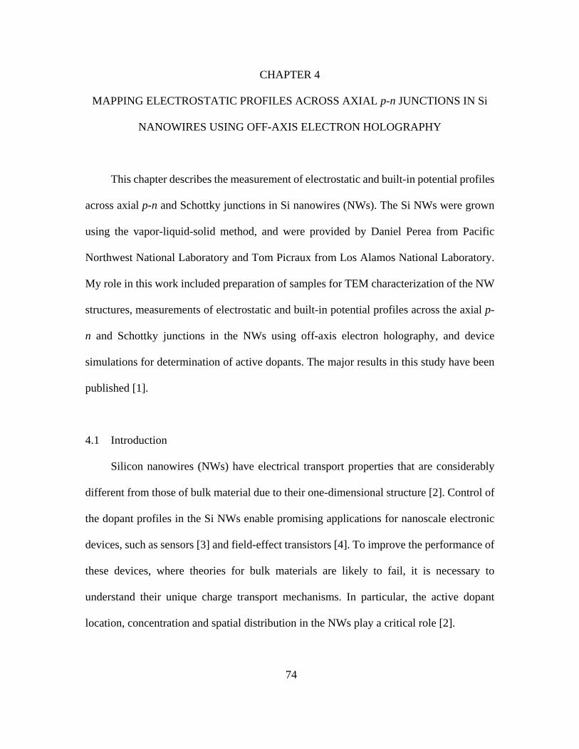
CHAPTER 4
MAPPING ELECTROSTATIC PROFILES ACROSS AXIAL p-n JUNCTIONS IN Si
NANOWIRES USING OFF-AXIS ELECTRON HOLOGRAPHY
This chapter describes the measurement of electrostatic and built-in potential profiles
across axial p-n and Schottky junctions in Si nanowires (NWs). The Si NWs were grown
using the vapor-liquid-solid method, and were provided by Daniel Perea from Pacific
Northwest National Laboratory and Tom Picraux from Los Alamos National Laboratory.
My role in this work included preparation of samples for TEM characterization of the NW
structures, measurements of electrostatic and built-in potential profiles across the axial p-
n and Schottky junctions in the NWs using off-axis electron holography, and device
simulations for determination of active dopants. The major results in this study have been
published [1].
4.1 Introduction
Silicon nanowires (NWs) have electrical transport properties that are considerably
different from those of bulk material due to their one-dimensional structure [2]. Control of
the dopant profiles in the Si NWs enable promising applications for nanoscale electronic
devices, such as sensors [3] and field-effect transistors [4]. To improve the performance of
these devices, where theories for bulk materials are likely to fail, it is necessary to
understand their unique charge transport mechanisms. In particular, the active dopant
location, concentration and spatial distribution in the NWs play a critical role [2].
74
Different experimental techniques have been used to characterize NW composition,
such as transmission electron microscopy (TEM), scanning TEM (STEM) [5], secondary
ion mass spectroscopy [6], and atom probe tomography [7]. However, it is difficult to make
direct measurements of the active dopant distribution and resultant electronic properties
within NWs because of their nanoscale dimensions. In addition, multiple junctions in real
devices can further complicate measurements. The technique of off-axis electron
holography provides an effective approach to quantitatively map electrostatic fields with
nanoscale spatial resolution, without the need for micro-fabricated electrical contacts [8,9].
In addition, the technique has recently been used to characterize the electrical properties of
different NWs [10-12].
Off-axis electron holography is a TEM-based interferometric technique [8,9]. In
cases where magnetic field is absent, and cylindrical NW shape as well as uniform
distribution in the NW cross section are assumed, the phase shift due to the sample can be
described by:
∆𝑖𝑖(𝑥𝑥,𝑦𝑦) = 𝐶𝐶𝐸𝐸 × (𝑉𝑉0(𝑥𝑥,𝑦𝑦, 𝑧𝑧) + 𝑉𝑉𝑏𝑏𝑖𝑖(𝑥𝑥,𝑦𝑦, 𝑧𝑧)) × t (4.1)
where CE is an electron-energy-dependent interaction constant with the value of 0.00728
rad V-1 nm-1 for 200-keV electrons, V0 is the mean inner potential (MIP) of the sample, Vbi
is the built-in potential and t is the diameter of NW served as the projected thickness.
In the case of a single p-n junction without bias, the built-in junction potential can be
calculated using the expression:
𝑉𝑉𝑏𝑏𝑖𝑖 = 𝑘𝑘×𝑘𝑘𝑒𝑒
× ln (𝑁𝑁𝐴𝐴×𝑁𝑁𝐷𝐷𝑛𝑛𝑖𝑖2 ) (4.2)
where k is Boltzmann’s constant, T is the absolute temperature, e is the electron charge, ni
is the intrinsic carrier concentration, and NA and ND are the acceptor and donor 75
concentrations [13]. Multiple junctions that are not far apart may cause the carriers to be
redistributed, such as for the case where a Schottky contact is located close to the p-n
junction. Furthermore, trap states at the native surface oxide/NW interface or within the
oxide itself will form a surface depletion region which further complicates transport
analysis [14,15]. Thus, more comprehensive simulations are necessary when charge
distributions and any changes in the sample geometry (eg. local NW thickness) are taken
into consideration. Careful comparison between simulation and experiment could then give
information about the distribution and concentration of the active dopants. In this study,
electron holography has been used to map the electrostatic field across the axial p-n
junction and the Au catalyst Schottky contact of a Si NW and estimates of the active dopant
concentrations have been extracted based on comparisons with simulations.
4.2 Experimental Details
Figure 4.1 Schematic diagram of the Si NW growth procedure: (a) Au particles were
deposited on Si substrate as catalysts; (b) n-type Si segment was grown using P as dopant;
(c) P source was switched off and a p-type Si segment was grown due to unintentional
dopant. 76
Figure 4.1 shows a schematic diagram of the Si NW growth procedure. The Si NWs
with axial p-n junctions were grown in a cold-wall chemical vapor deposition reactor via
the vapor-liquid-solid (VLS) method using 30-60 nm diameter Au colloid nanoparticle
catalysts on silicon (111) substrates. The growth sequence is as follows. A ~10-μm-long
phosphorus-doped (n-type) Si segment was initially grown using the gas mixture of SiH4
and PH3 at a growth temperature of 550°C and total pressure of 3 Torr. A partial pressure
ratio of PH3/SiH4 = 5.3 × 10⁻³ was used which would result in an estimated doping
concentration of ~1019 cm-3. The PH3 gas was then turned off, and a ~300-nm segment of
pure unintentionally-doped Si was grown before termination of growth. For unintentional
doping, the pure Si segment tends to be p-type as a result of electrical trap defects near the
interface due to the presence of a thin oxide layer on the NW surface; the corresponding
dopant concentration was estimated to be roughly 1017 to 1018cm-3 [Ref. 15]. A p-n junction
should thus be formed in the Si NW at a distance of about 300 nm away from the Au
catalyst at the tip of the NW. For TEM analysis, the NWs were ultrasonicated in isopropyl
alcohol and transferred via pipette to TEM copper mesh grids with holey carbon support
films, and air-dried before observation.
Electron microscopy and off-axis electron holography characterization were carried
out using FEI CM200 and Tecnai F20 TEMs equipped with electrostatic biprisms and
operated at 200 kV. Holograms were taken using the Lorentz mini-lens with the objective
lens switched off to obtain a larger field of view. The typical biprism voltage was 120 V
giving a fringe spacing of about 5nm at the usual magnification of 20kX. The exposure
time for hologram recording was 2s.
77
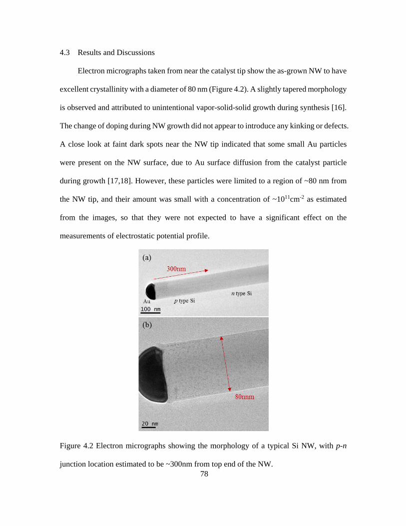
4.3 Results and Discussions
Electron micrographs taken from near the catalyst tip show the as-grown NW to have
excellent crystallinity with a diameter of 80 nm (Figure 4.2). A slightly tapered morphology
is observed and attributed to unintentional vapor-solid-solid growth during synthesis [16].
The change of doping during NW growth did not appear to introduce any kinking or defects.
A close look at faint dark spots near the NW tip indicated that some small Au particles
were present on the NW surface, due to Au surface diffusion from the catalyst particle
during growth [17,18]. However, these particles were limited to a region of ~80 nm from
the NW tip, and their amount was small with a concentration of ~1011cm-2 as estimated
from the images, so that they were not expected to have a significant effect on the
measurements of electrostatic potential profile.
Figure 4.2 Electron micrographs showing the morphology of a typical Si NW, with p-n
junction location estimated to be ~300nm from top end of the NW. 78
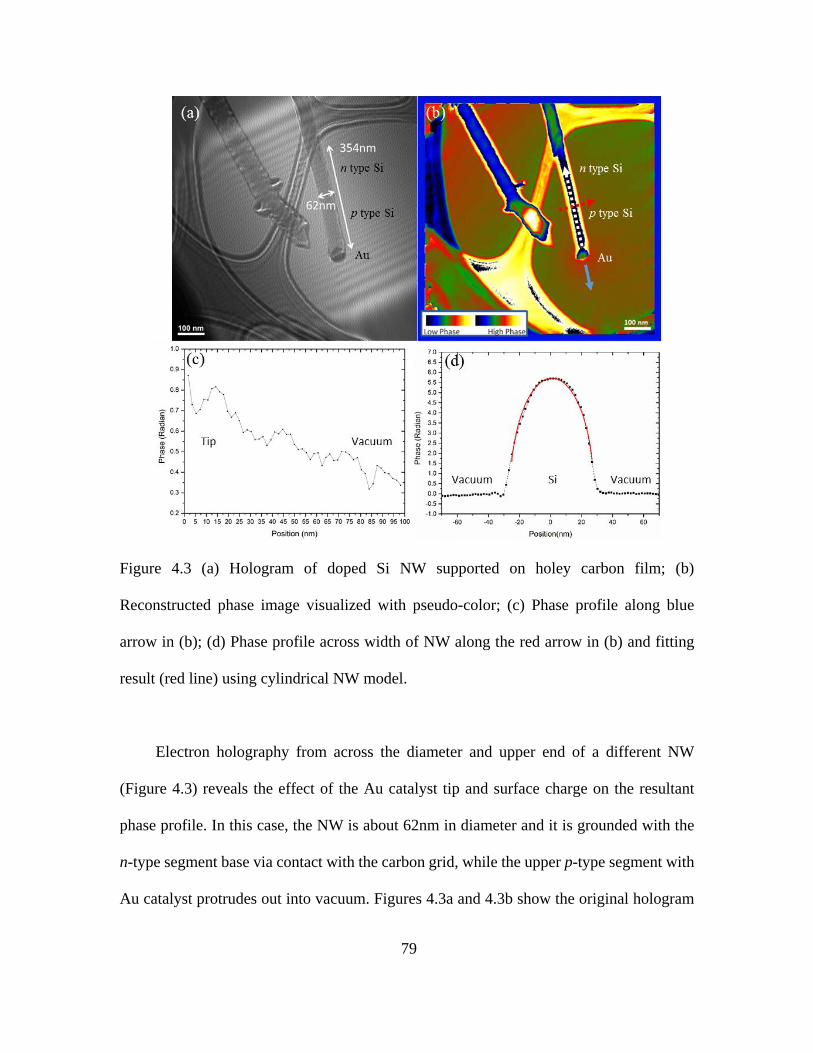
Figure 4.3 (a) Hologram of doped Si NW supported on holey carbon film; (b)
Reconstructed phase image visualized with pseudo-color; (c) Phase profile along blue
arrow in (b); (d) Phase profile across width of NW along the red arrow in (b) and fitting
result (red line) using cylindrical NW model.
Electron holography from across the diameter and upper end of a different NW
(Figure 4.3) reveals the effect of the Au catalyst tip and surface charge on the resultant
phase profile. In this case, the NW is about 62nm in diameter and it is grounded with the
n-type segment base via contact with the carbon grid, while the upper p-type segment with
Au catalyst protrudes out into vacuum. Figures 4.3a and 4.3b show the original hologram
79
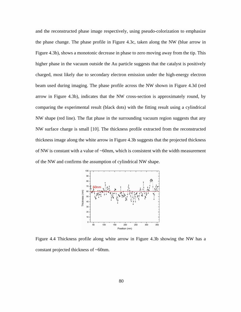
and the reconstructed phase image respectively, using pseudo-colorization to emphasize
the phase change. The phase profile in Figure 4.3c, taken along the NW (blue arrow in
Figure 4.3b), shows a monotonic decrease in phase to zero moving away from the tip. This
higher phase in the vacuum outside the Au particle suggests that the catalyst is positively
charged, most likely due to secondary electron emission under the high-energy electron
beam used during imaging. The phase profile across the NW shown in Figure 4.3d (red
arrow in Figure 4.3b), indicates that the NW cross-section is approximately round, by
comparing the experimental result (black dots) with the fitting result using a cylindrical
NW shape (red line). The flat phase in the surrounding vacuum region suggests that any
NW surface charge is small [10]. The thickness profile extracted from the reconstructed
thickness image along the white arrow in Figure 4.3b suggests that the projected thickness
of NW is constant with a value of ~60nm, which is consistent with the width measurement
of the NW and confirms the assumption of cylindrical NW shape.
Figure 4.4 Thickness profile along white arrow in Figure 4.3b showing the NW has a
constant projected thickness of ~60nm.
80
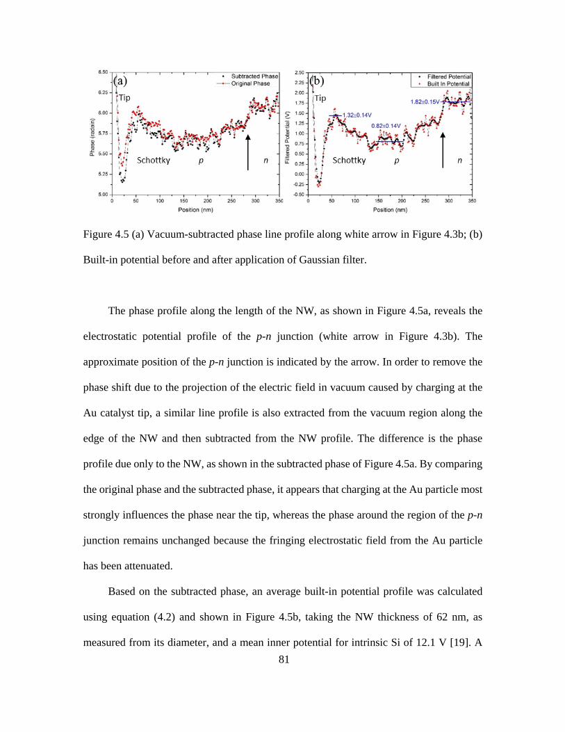
Figure 4.5 (a) Vacuum-subtracted phase line profile along white arrow in Figure 4.3b; (b)
Built-in potential before and after application of Gaussian filter.
The phase profile along the length of the NW, as shown in Figure 4.5a, reveals the
electrostatic potential profile of the p-n junction (white arrow in Figure 4.3b). The
approximate position of the p-n junction is indicated by the arrow. In order to remove the
phase shift due to the projection of the electric field in vacuum caused by charging at the
Au catalyst tip, a similar line profile is also extracted from the vacuum region along the
edge of the NW and then subtracted from the NW profile. The difference is the phase
profile due only to the NW, as shown in the subtracted phase of Figure 4.5a. By comparing
the original phase and the subtracted phase, it appears that charging at the Au particle most
strongly influences the phase near the tip, whereas the phase around the region of the p-n
junction remains unchanged because the fringing electrostatic field from the Au particle
has been attenuated.
Based on the subtracted phase, an average built-in potential profile was calculated
using equation (4.2) and shown in Figure 4.5b, taking the NW thickness of 62 nm, as
measured from its diameter, and a mean inner potential for intrinsic Si of 12.1 V [19]. A 81
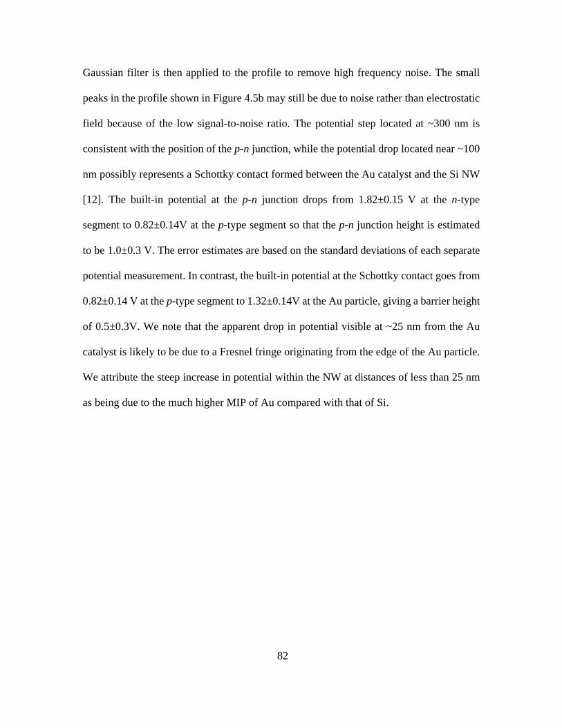
Gaussian filter is then applied to the profile to remove high frequency noise. The small
peaks in the profile shown in Figure 4.5b may still be due to noise rather than electrostatic
field because of the low signal-to-noise ratio. The potential step located at ~300 nm is
consistent with the position of the p-n junction, while the potential drop located near ~100
nm possibly represents a Schottky contact formed between the Au catalyst and the Si NW
[12]. The built-in potential at the p-n junction drops from 1.82±0.15 V at the n-type
segment to 0.82±0.14V at the p-type segment so that the p-n junction height is estimated
to be 1.0±0.3 V. The error estimates are based on the standard deviations of each separate
potential measurement. In contrast, the built-in potential at the Schottky contact goes from
0.82±0.14 V at the p-type segment to 1.32±0.14V at the Au particle, giving a barrier height
of 0.5±0.3V. We note that the apparent drop in potential visible at ~25 nm from the Au
catalyst is likely to be due to a Fresnel fringe originating from the edge of the Au particle.
We attribute the steep increase in potential within the NW at distances of less than 25 nm
as being due to the much higher MIP of Au compared with that of Si.
82
Figure 4.6 (a) Schematic showing cross section of model used for simulations consisting
of Si NW with p-n junction, grounded on the n-side and biased on the Au particle at the
end of the p-doped region; (b) Experimental built-in potential profile and simulated profiles
for different dopant concentrations at p-n junction, work function 𝜙𝜙 =4.6 V; (c) Simulated
built-in potential profiles with different gradient widths, dopant concentrations NA=1017
cm-3, ND=1019 cm-3, and work function 𝜙𝜙 =4.6 V. Two layers in the dopant concentrations
of ND=1018 cm-3 and ND=1017 cm-3, respectively, are added after n-type region with layer
widths as shown in the legend.
In order to better interpret the electrostatic potential profiles, simulations of the NW
potential distribution were performed using the SilvacoTM software package. The
parameters for the simulation are schematically illustrated in Figure 4.6a. The Si NW was
simulated as a cylinder with a diameter of 62 nm and an SiO2 shell of 5 nm. The SiO2 was
used to define surface charge so that its thickness should not influence the results. Since 83
the effect of the surface charge was not apparent in the experimental results, the surface
charge in the simulation was defined to be zero at the interface between Si and SiO2. The
validity of this assumption was tested by additional simulations with varying surface
charges, as discussed below. The n-type segment of the Si NW was connected to ground,
while the p-type segment was connected to Au via a Schottky contact with bias applied to
the Au contact. An abrupt junction model was initially used in the simulations, but a non-
abrupt junction was later tested and did not affect the overall trend of the results. The donor
concentration, acceptor concentration, Au work function and bias were then systematically
adjusted in order to find a match with the experimental electrostatic profile.
As shown by the magenta hexagrams in Figure 4.6b, a donor concentration of ~1019
cm-3, an acceptor concentration of ~1017 cm-3, a work function of 4.6 V and 0 V bias gave
the best fit to the experimental profile. The corresponding simulated built-in potential
height and depletion length for the p-n junction were 0.93 V and 120 nm, respectively, and
0.51 V and 100 nm for the Schottky contact, respectively. These values are consistent with
the experimental values. Most of the depletion region was located on the lower
concentration, p side. Since the distance between the p-n junction and the Schottky contact
is ~250 nm, they should not have any significant effect on each other. By using Equation
4.3, the built-in potential due to single p-n junction can also be calculated to be ~1V with
a depletion region width of ~112nm, which confirms the simulation results above. When
the simulated acceptor concentration is lower than 1017 cm-3 (refer to colored points) or the
donor concentration is lower than 1019 cm-3 (refer to colored points), then the depletion
regions across the p-n junction and the Schottky contact are larger and the built-in potential
changes less rapidly, resulting in a higher potential in the p-type region than measured
84
experimentally. Conversely, when the simulated acceptor concentration is greater than 1017
cm-3 (refer to colored points) or donor concentration is greater than 1019 cm-3 (refer to
colored points), the depletion region of the p-n junction and the Schottky contact are
smaller and the built-in potential changes more rapidly, giving deeper potential in the p-
type region than measured.
Any change in dopant concentration during VLS growth usually results in an
exponentially-decreasing gradient at the interface [20-22], with a length that is comparable
to the NW diameter, which is ~60 nm in this case, forming an n+-n--p junction. To assess
the effect of such gradients, two n-type segments with concentrations of 1018 cm-3 and 1017
cm-3, respectively, were added in the simulations between the n-type and p-type segments,
as shown in Figure 4.6c. The simulations suggest that the short n- portion is fully depleted
and has only a small effect on the p-n junction, making the junction slightly flatter in the
middle. As the gradients become longer, the flatter part is extended further into the p-type
segment. Because the total depletion length is very long compared to the gradient due to
low concentration on the p side, the gradients do not have a significant effect on the
junction height nor the total depletion width.
85
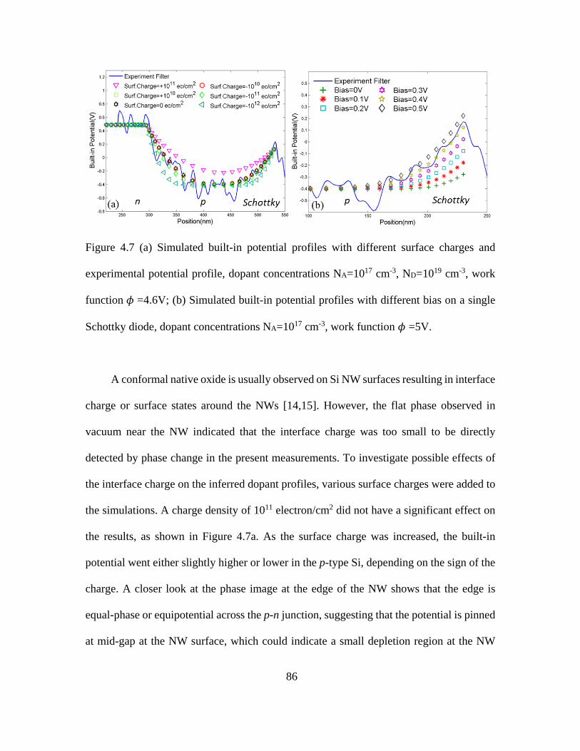
Figure 4.7 (a) Simulated built-in potential profiles with different surface charges and
experimental potential profile, dopant concentrations NA=1017 cm-3, ND=1019 cm-3, work
function 𝜙𝜙 =4.6V; (b) Simulated built-in potential profiles with different bias on a single
Schottky diode, dopant concentrations NA=1017 cm-3, work function 𝜙𝜙 =5V.
A conformal native oxide is usually observed on Si NW surfaces resulting in interface
charge or surface states around the NWs [14,15]. However, the flat phase observed in
vacuum near the NW indicated that the interface charge was too small to be directly
detected by phase change in the present measurements. To investigate possible effects of
the interface charge on the inferred dopant profiles, various surface charges were added to
the simulations. A charge density of 1011 electron/cm2 did not have a significant effect on
the results, as shown in Figure 4.7a. As the surface charge was increased, the built-in
potential went either slightly higher or lower in the p-type Si, depending on the sign of the
charge. A closer look at the phase image at the edge of the NW shows that the edge is
equal-phase or equipotential across the p-n junction, suggesting that the potential is pinned
at mid-gap at the NW surface, which could indicate a small depletion region at the NW
86
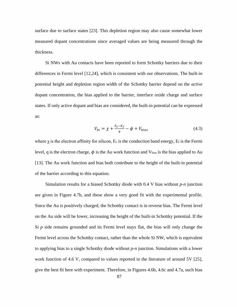
surface due to surface states [23]. This depletion region may also cause somewhat lower
measured dopant concentrations since averaged values are being measured through the
thickness.
Si NWs with Au contacts have been reported to form Schottky barriers due to their
differences in Fermi level [12,24], which is consistent with our observations. The built-in
potential height and depletion region width of the Schottky barrier depend on the active
dopant concentration, the bias applied to the barrier, interface oxide charge and surface
states. If only active dopant and bias are considered, the built-in potential can be expressed
as:
𝑉𝑉𝑏𝑏𝑖𝑖 = 𝜒𝜒 + 𝐸𝐸𝑐𝑐−𝐸𝐸𝑓𝑓𝑞𝑞
− 𝜙𝜙 + 𝑉𝑉𝑏𝑏𝑖𝑖𝑠𝑠𝑠𝑠 (4.3)
where χ is the electron affinity for silicon, Ec is the conduction band energy, Ef is the Fermi
level, q is the electron charge, 𝜙𝜙 is the Au work function and Vbias is the bias applied to Au
[13]. The Au work function and bias both contribute to the height of the built-in potential
of the barrier according to this equation.
Simulation results for a biased Schottky diode with 0.4 V bias without p-n junction
are given in Figure 4.7b, and these show a very good fit with the experimental profile.
Since the Au is positively charged, the Schottky contact is in reverse bias. The Fermi level
on the Au side will be lower, increasing the height of the built-in Schottky potential. If the
Si p side remains grounded and its Fermi level stays flat, the bias will only change the
Fermi level across the Schottky contact, rather than the whole Si NW, which is equivalent
to applying bias to a single Schottky diode without p-n junction. Simulations with a lower
work function of 4.6 V, compared to values reported in the literature of around 5V [25],
give the best fit here with experiment. Therefore, in Figures 4.6b, 4.6c and 4.7a, such bias 87
can be considered as a change of work function in the simulation that keeps the Fermi level
flat across the p-n junction.
4.4 Conclusions
Si NWs have been grown with axial p-n junctions using the VLS method. A Schottky
junction is formed at the end of the NW due to the presence of the Au catalyst particle. The
electrostatic potential profile measured by electron holography shows that the built-in
potentials across the p-n junction and the Schottky junction, have values of 1.0±0.3 V and
0.5±0.3 V, respectively. Simulations indicate that the dopant concentrations are ~1019cm-3
for donor and ~1017 cm-3 for acceptor. The positively charged Au particle at the end of the
grounded NW is considered to account for the lower work function in the simulation. The
effects of a possible transition region forming n+-n--p junction and possible surface charge
were also systematically studied by simulations. Overall, these results demonstrated that
the off-axis electron holography technique can provide valuable information on the
electrically active dopant distributions in NW device structures.
88
References
[1] Z. Gan, D. E. Perea, J. Yoo, S. Tom Picraux, D. J. Smith, and M. R. McCartney, Applied Physics Letters 103 153108 (2013).
[2] V. Schmidt, J. V. Wittemann, S. Senz, and U. Gösele, Advanced Materials 21 2681 (2009).
[3] Y. Cui, Q. Wei, H. Park, and C. M. Lieber, Science 293 1289 (2001).
[4] J. Goldberger, A. I. Hochbaum, R. Fan, and P. Yang, Nano letters 6 973 (2006).
[5] P. M. Voyles, D. A. Muller, J. L. Grazul, P. H. Citrin, and H. J. Gossmann, Nature 416 826 (2002).
[6] T. Tanaka, N. Murata, K. Saito, M. Nishio, Q. Guo, and H. Ogawa, physica status solidi (b) 244 1685 (2007).
[7] D. E. Perea, E. R. Hemesath, E. J. Schwalbach, J. L. Lensch-Falk, P. W. Voorhees, and L. J. Lauhon, Nature nanotechnology 4 315 (2009).
[8] M. R. McCartney and D. J. Smith, Annual Review of Materials Research 37 729 (2007).
[9] M. R. McCartney, N. Agarwal, S. Chung, D. A. Cullen, M.-G. Han, K. He, L. Li, H. Wang, L. Zhou, and D. J. Smith, Ultramicroscopy 110 375 (2010).
[10] M. I. den Hertog, H. Schmid, D. Cooper, J.-L. Rouviere, M. T. Björk, H. Riel, P. Rivallin, S. Karg, and W. Riess, Nano letters 9 3837 (2009).
[11] L. Li, D. J. Smith, E. Dailey, P. Madras, J. Drucker, and M. R. McCartney, Nano letters 11 493 (2011).
[12] H. Kai, C. Jeong-Hyun, J. Yeonwoong, S. T. Picraux, and C. John, Nanotechnology 24 115703 (2013).
[13] S. M. Sze, Physics of semiconductor devices. Wiley-Interscience, New York, (1969).
[14] I. Kimukin, M. S. Islam, and R. S. Williams, Nanotechnology 17 S240 (2006).
[15] S. Ingole, P. Manandhar, S. B. Chikkannanavar, E. A. Akhadov, and S. T. Picraux, Electron Devices, IEEE Transactions on 55 2931 (2008).
[16] S. A. Dayeh, J. Wang, N. Li, J. Y. Huang, A. V. Gin, and S. T. Picraux, Nano letters 11 4200 (2011).
89
[17] S. A. Dayeh, N. H. Mack, J. Y. Huang, and S. T. Picraux, Applied Physics Letters 99 023102 (2011).
[18] J. E. Allen, E. R. Hemesath, D. E. Perea, J. L. Lensch-Falk, Z. Y. Li, F. Yin, M. H. Gass, P. Wang, A. L. Bleloch, R. E. Palmer, and L. J. Lauhon, Nature nanotechnology 3 168 (2008).
[19] J. Li, M. R. McCartney, and D. J. Smith, Ultramicroscopy 94 149 (2003).
[20] T. E. Clark, P. Nimmatoori, K.-K. Lew, L. Pan, J. M. Redwing, and E. C. Dickey, Nano letters 8 1246 (2008).
[21] D. E. Perea, N. Li, R. M. Dickerson, A. Misra, and S. T. Picraux, Nano letters 11 3117 (2011).
[22] N. Li, T. Y. Tan, and U. Gösele, Applied Physics A 90 591 (2008).
[23] D. Cooper, C. Ailliot, J.-P. Barnes, J.-M. Hartmann, P. Salles, G. Benassayag, and R. E. Dunin-Borkowski, Ultramicroscopy 110 383 (2010).
[24] E. Koren, N. Berkovitch, O. Azriel, A. Boag, Y. Rosenwaks, E. R. Hemesath, and L. J. Lauhon, Applied Physics Letters 99 223511 (2011).
[25] P. A. Tipler, Modern physics. Worth Publishers, New York, (1978).
90
CHAPTER 5
MEASUREMENT OF ACTIVE DOPANTS IN AXIAL Si-Ge NANOWIRE
HETEROJUNCTIONS USING OFF-AXIS ELECTRON HOLOGRAPHY AND
ATOM-PROBE TOMOGRAPHY
This chapter describes the measurement of active dopants in axial Si-Ge nanowire
(NW) heterojunctions using off-axis electron holography and atom-probe tomography. The
axial Si-Ge NWs were grown using the vapor-liquid-solid method, and were provided by
Daniel Perea from Pacific Northwest National Laboratory, Jinkyoung Yoo and Tom
Picraux from Los Alamos National Laboratory. The atom-probe tomography experiment
was performed by Daniel Perea. My role in this work included preparation of TEM samples,
characterization of the NW structures, measurements of electrostatic and built-in potential
profiles across the hererojunction and Schottky junctions in axial Si-Ge NWs using off-
axis electron holography, and device simulations for active dopant determination. The main
results of this work have been submitted for publication [1].
5.1 Introduction
Semiconductor heterostructures have many novel and attractive applications
compared with individual semiconductors such as Si due to their ability to tune electronic
transport properties by varying composition in addition to dopant type and concentration
[2]. Si-Ge axial heterojunction nanowires (NWs) are considered as potential high-
performance transistor devices because Ge has low effective mass, high mobility and small
band gap compared with Si [3]. Moreover, the NW geometry can reduce the density of
91
dislocations caused by lattice mismatch [2], and also provide new options for 3D device
integration [4,5]. Axial Si/Ge NW heterojunctions with abrupt interfaces have been grown
using the vapor-liquid-solid (VLS) [6] and vapor-solid-solid (VSS) methods [7]. Changes
in electronic transport properties have been achieved with different dopant profiles by
growing Ge NWs on Si pillars formed by etching [8]. To improve the engineering and
performance of Si-Ge NW integrated devices, it is necessary to understand their charge
transport mechanisms. In particular, knowledge of active dopant profiles and the resultant
built-in potential can play a critical role.
The present study has used off-axis electron holography (EH) to measure the built-in
electrostatic potential across doped Si-Ge NW heterojunctions with/without in situ bias, in
combination with atom-probe tomography (APT) to measure the total dopant distributions.
The active dopant profiles were then extracted by comparing the experimental results with
TCAD simulations.
5.2 Experimental Details
Figure 5.1 shows a schematic diagram of the NW growth procedure. The axial Si-Ge
heterojunction NWs were grown using the VLS method in a cold-wall CVD reactor [6].
The growth process was as follows. First, Si (111) substrates were solvent-cleaned and
native-oxide-etched. Then Au colloid nanoparticles were dispersed as catalysts on the
substrate surface. Germane (GeH4) diluted in hydrogen (H2) with a concentration of 30%
was introduced into the chamber, while the total pressure was maintained at 3 Torr. The Ge
<111> NW growth was initiated at 340℃ for 3min followed by further growth at 280℃ for
20−30mins. 100 ppm diborane (B2H6) diluted in H2 was also introduced to provide a p-
92
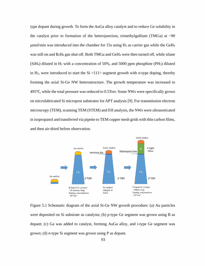
type dopant during growth. To form the AuGa alloy catalyst and to reduce Ge solubility in
the catalyst prior to formation of the heterojunction, trimethylgallium (TMGa) at ~90
μmol/min was introduced into the chamber for 15s using H2 as carrier gas while the GeH4
was still on and B2H6 gas shut off. Both TMGa and GeH4 were then turned off, while silane
(SiH4) diluted in H2 with a concentration of 50%, and 5000 ppm phosphine (PH3) diluted
in H2, were introduced to start the Si <111> segment growth with n-type doping, thereby
forming the axial Si-Ge NW heterostructure. The growth temperature was increased to
495℃, while the total pressure was reduced to 0.5Torr. Some NWs were specifically grown
on microfabricated Si micropost substrates for APT analysis [9]. For transmission electron
microscopy (TEM), scanning TEM (STEM) and EH analysis, the NWs were ultrasonicated
in isopropanol and transferred via pipette to TEM copper mesh grids with thin carbon films,
and then air-dried before observation.
Figure 5.1 Schematic diagram of the axial Si-Ge NW growth procedure: (a) Au particles
were deposited on Si substrate as catalysts; (b) p-type Ge segment was grown using B as
dopant; (c) Ga was added to catalyst, forming AuGa alloy, and i-type Ge segment was
grown; (d) n-type Si segment was grown using P as dopant. 93
Atom probe tomography (APT) is currently the only technique that can directly
quantify the relative composition and distribution of dopants within nanowires [10]. Here
we have used APT to measure the total dopant profile along the nanowire growth axis
across the Si-Ge heterojunction. Due to a combined limitation in detection efficiency and
spatial resolution, APT analysis cannot provide information about the bonding
environment of the dopants, and thus cannot provide information about whether dopants
are interstitially (electrically inactive) or substitutionally (electrically active) incorporated.
Thus, APT only provides the total dopant composition. However, when combined with EH
which can be used to estimate the composition of electrically active dopants, any
differences between the two techniques can lead to an estimate of doping efficiency.
Determination of the electrically active dopants in the Si-Ge NWs is an important
step towards useful device applications. Off-axis electron holography is an interferometric
TEM technique that can provide amplitude and phase information about the sample under
observation [11,12]. By using the reconstructed phase image, the electrostatic potential
profile and thus the built-in potential of the sample, can be measured and compared with
simulations to estimate the active dopant concentrations. For a non-magnetic sample and
assuming that the potentials are distributed uniformly across the projected thickness, the
phase shift in a reconstructed phase image can be simplified to:
∆𝑖𝑖(𝑥𝑥,𝑦𝑦) = 𝐶𝐶𝐸𝐸 × (𝑉𝑉0(𝑥𝑥,𝑦𝑦, 𝑧𝑧) + 𝑉𝑉𝑏𝑏𝑖𝑖(𝑥𝑥,𝑦𝑦, 𝑧𝑧)) × 𝑎𝑎 (5.1)
where CE is an electron-energy-dependent interaction constant having the value of 0.00653
rad. V-1. nm-1 for 300-keV electrons, V0 is the mean inner potential (MIP) of the sample
caused by incomplete screening of atomic cores, Vbi is the built-in electrostatic potential
resulting from any electric field and/or charge accumulation in the sample and t is the
94
projected sample thickness [12]. The EH technique has been widely used for characterizing
electrostatic potential profiles in nanoscale semiconductors [13-15].
TEM, STEM and EH studies were done using an FEI Titan 80-300 equipped with a
Schottky field-emission electron gun, probe corrector, Lorentz mini-lens and electrostatic
biprism. The EH experiments were performed using the Lorentz mini-lens with the normal
objective lens switched off in order to obtain a larger field of view. The biprism voltage
was typically 120 V, giving 2.5-nm interference-fringe spacing, and the hologram exposure
time was 2 s. APT analysis was performed using a LEAP 4000X-HR. A 355-nm UV laser
pulsed at 200 kHz was used to initiate thermally-assisted field evaporation at a detection
rate of 0.005 ions/pulse. A more detailed description of the APT analysis of NWs is given
in reference [10].
5.3 Results and Discussions
Figures 5.2a and 5.2c show STEM HAADF images of a typical straight axial Si-Ge
NW, which was grown using the same procedure but at different temperature. The tapered
Ge segment is not obvious in this case. The grey region at the Si-Ge heterojunction
indicates that the Ge-Si transition region is short and faceted. Catalyst materials are
observable as small bright dots on the Ge surface, which is likely due to diffusion from the
catalyst particle during the growth. EDX profiles were extracted across the Si-Ge
heterojunction (Figure 5.2b) and the Si-catalyst interface (Figure 5.2d), along the blue
arrows in Figures 5.2a and 5.2c, respectively. The EDX profile across the heterojunction
suggests that the Si-Ge transition region is ~50nm long, which is short compared to growth
using Au catalysts, which are usually on the size of the NW diameter (~110nm) [16]. The
95
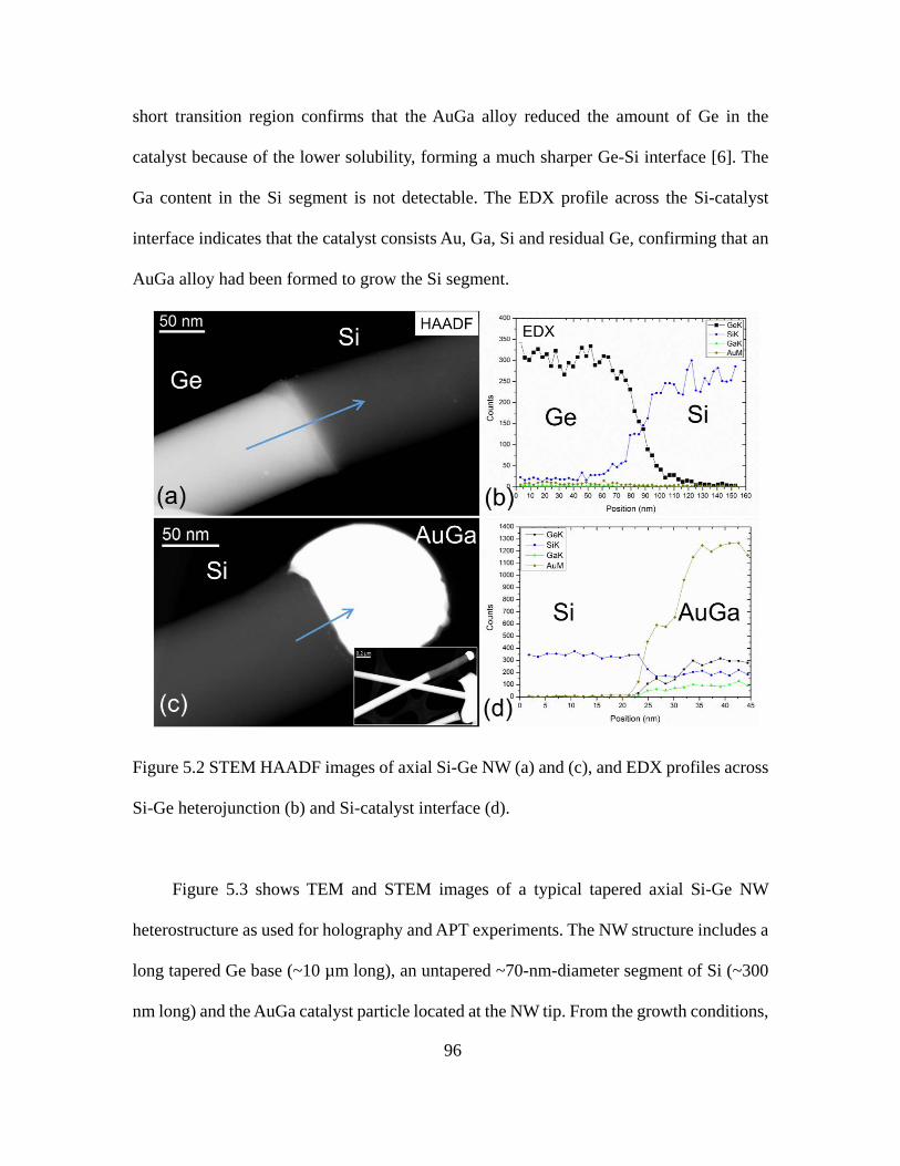
short transition region confirms that the AuGa alloy reduced the amount of Ge in the
catalyst because of the lower solubility, forming a much sharper Ge-Si interface [6]. The
Ga content in the Si segment is not detectable. The EDX profile across the Si-catalyst
interface indicates that the catalyst consists Au, Ga, Si and residual Ge, confirming that an
AuGa alloy had been formed to grow the Si segment.
Figure 5.2 STEM HAADF images of axial Si-Ge NW (a) and (c), and EDX profiles across
Si-Ge heterojunction (b) and Si-catalyst interface (d).
Figure 5.3 shows TEM and STEM images of a typical tapered axial Si-Ge NW
heterostructure as used for holography and APT experiments. The NW structure includes a
long tapered Ge base (~10 µm long), an untapered ~70-nm-diameter segment of Si (~300
nm long) and the AuGa catalyst particle located at the NW tip. From the growth conditions,
96
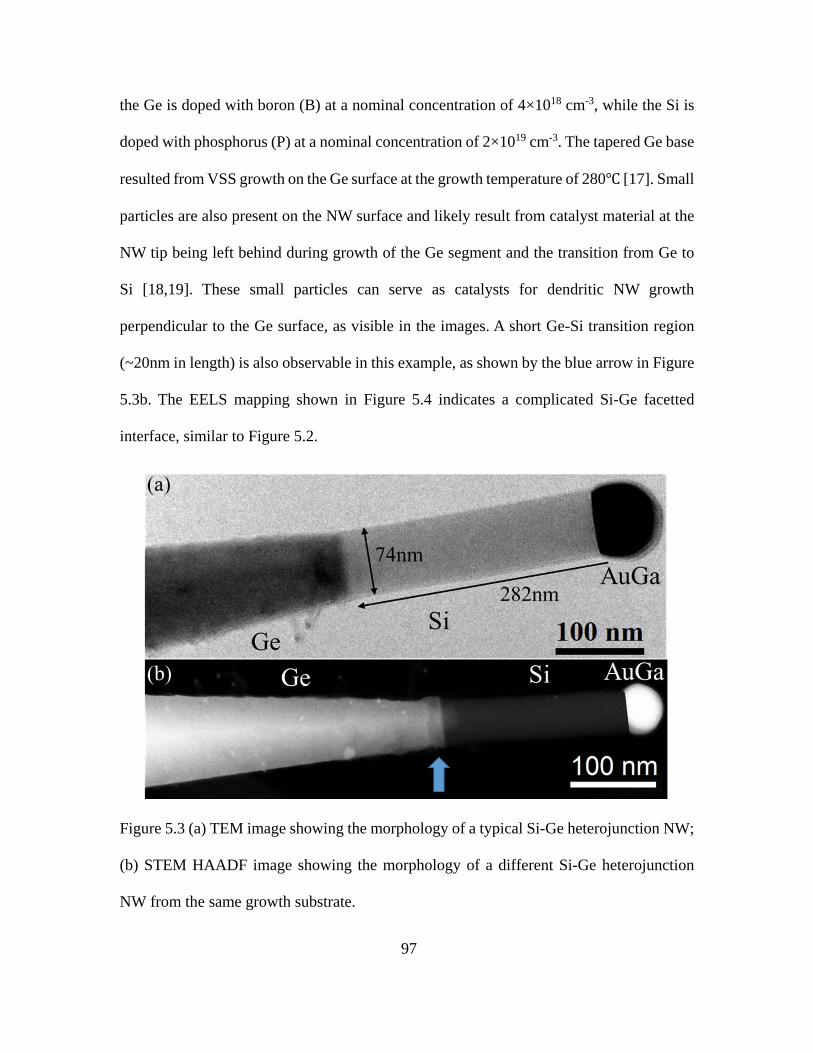
the Ge is doped with boron (B) at a nominal concentration of 4×1018 cm-3, while the Si is
doped with phosphorus (P) at a nominal concentration of 2×1019 cm-3. The tapered Ge base
resulted from VSS growth on the Ge surface at the growth temperature of 280℃ [17]. Small
particles are also present on the NW surface and likely result from catalyst material at the
NW tip being left behind during growth of the Ge segment and the transition from Ge to
Si [18,19]. These small particles can serve as catalysts for dendritic NW growth
perpendicular to the Ge surface, as visible in the images. A short Ge-Si transition region
(~20nm in length) is also observable in this example, as shown by the blue arrow in Figure
5.3b. The EELS mapping shown in Figure 5.4 indicates a complicated Si-Ge facetted
interface, similar to Figure 5.2.
Figure 5.3 (a) TEM image showing the morphology of a typical Si-Ge heterojunction NW;
(b) STEM HAADF image showing the morphology of a different Si-Ge heterojunction
NW from the same growth substrate.
97
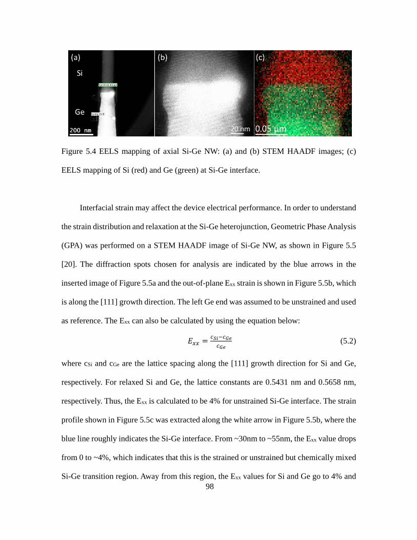
Figure 5.4 EELS mapping of axial Si-Ge NW: (a) and (b) STEM HAADF images; (c)
EELS mapping of Si (red) and Ge (green) at Si-Ge interface.
Interfacial strain may affect the device electrical performance. In order to understand
the strain distribution and relaxation at the Si-Ge heterojunction, Geometric Phase Analysis
(GPA) was performed on a STEM HAADF image of Si-Ge NW, as shown in Figure 5.5
[20]. The diffraction spots chosen for analysis are indicated by the blue arrows in the
inserted image of Figure 5.5a and the out-of-plane Exx strain is shown in Figure 5.5b, which
is along the [111] growth direction. The left Ge end was assumed to be unstrained and used
as reference. The Exx can also be calculated by using the equation below:
𝐸𝐸𝑚𝑚𝑚𝑚 = 𝑐𝑐𝑆𝑆𝑖𝑖−𝑐𝑐𝐺𝐺𝑟𝑟𝑐𝑐𝐺𝐺𝑟𝑟
(5.2)
where cSi and cGe are the lattice spacing along the [111] growth direction for Si and Ge,
respectively. For relaxed Si and Ge, the lattice constants are 0.5431 nm and 0.5658 nm,
respectively. Thus, the Exx is calculated to be 4% for unstrained Si-Ge interface. The strain
profile shown in Figure 5.5c was extracted along the white arrow in Figure 5.5b, where the
blue line roughly indicates the Si-Ge interface. From ~30nm to ~55nm, the Exx value drops
from 0 to ~4%, which indicates that this is the strained or unstrained but chemically mixed
Si-Ge transition region. Away from this region, the Exx values for Si and Ge go to 4% and 98
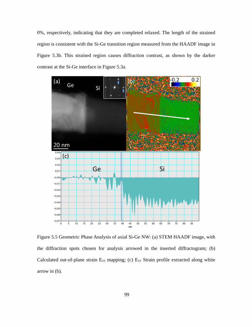
0%, respectively, indicating that they are completed relaxed. The length of the strained
region is consistent with the Si-Ge transition region measured from the HAADF image in
Figure 5.3b. This strained region causes diffraction contrast, as shown by the darker
contrast at the Si-Ge interface in Figure 5.3a.
Figure 5.5 Geometric Phase Analysis of axial Si-Ge NW: (a) STEM HAADF image, with
the diffraction spots chosen for analysis arrowed in the inserted diffractogram; (b)
Calculated out-of-plane strain Exx mapping; (c) Exx Strain profile extracted along white
arrow in (b).
99
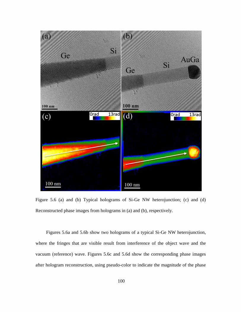
Figure 5.6 (a) and (b) Typical holograms of Si-Ge NW heterojunction; (c) and (d)
Reconstructed phase images from holograms in (a) and (b), respectively.
Figures 5.6a and 5.6b show two holograms of a typical Si-Ge NW heterojunction,
where the fringes that are visible result from interference of the object wave and the
vacuum (reference) wave. Figures 5.6c and 5.6d show the corresponding phase images
after hologram reconstruction, using pseudo-color to indicate the magnitude of the phase
100
change. The observed change in phase not only results from accumulated charge and/or
internal electric field, but also from changes in specimen thickness and chemistry. In Figure
5.6c, the phase within the Ge segment increases towards the left, because of the increasing
NW diameter. Some small dendritic growth is also visible on the Ge surface, which adds
significant noise to the analysis carried out below. No dendrite growth is observed on the
Si side in Figure 5.6d. Instead, the diameter of the Si NW increases slightly towards the
catalyst. The phase at the NW center also increases slightly, as shown by the red color.
The change in width as a function of distance for the Ge and Si segments, as well as
the corresponding phase profile, were extracted from left to right at the center of the NW,
along the white arrows in Figures 5.6c and 5.6d, respectively. These results were then
combined together, as shown in Figure 5.7a, where the phase is shown in black and the
width is shown in red. In order to reduce the effect of noise caused by the surface dendrite
growth, linear fitting is applied to the measured Ge width profile while constant width is
used for the Si part (shown by the blue line). By assuming that the NW has a cylindrical
shape, then its width can be used as the NW thickness projected along the electron-beam
direction. The change of phase is proportional to the change in width, where a monotonic
decrease in the phase profile with decreasing width is observed in the Ge segment,
consistent with the tapered NW geometry. A deviation in the phase profile is observed at
the heterointerface position of ~400nm, which is attributed to the difference in MIP
between Ge (14.3V) [21] and Si (12.1V) [22], in addition to the built-in potential. The Si
portion has almost constant diameter and phase except for the NW part located near the
catalyst, where these increase slightly.
101
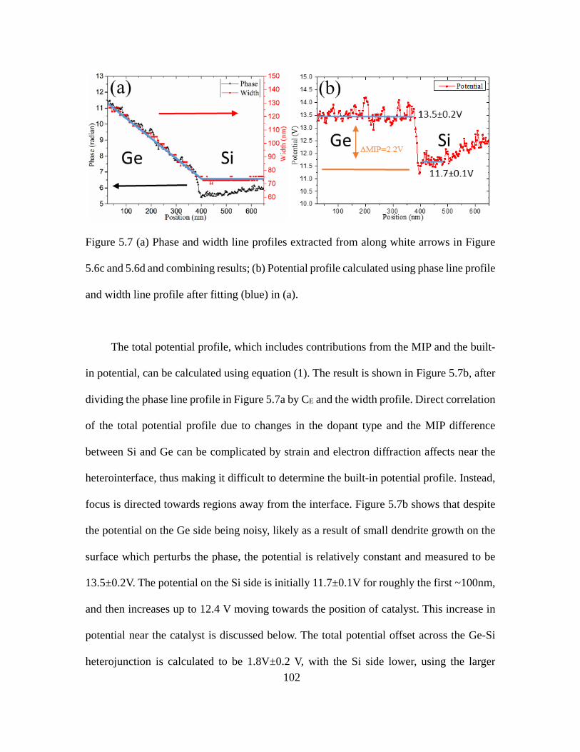
Figure 5.7 (a) Phase and width line profiles extracted from along white arrows in Figure
5.6c and 5.6d and combining results; (b) Potential profile calculated using phase line profile
and width line profile after fitting (blue) in (a).
The total potential profile, which includes contributions from the MIP and the built-
in potential, can be calculated using equation (1). The result is shown in Figure 5.7b, after
dividing the phase line profile in Figure 5.7a by CE and the width profile. Direct correlation
of the total potential profile due to changes in the dopant type and the MIP difference
between Si and Ge can be complicated by strain and electron diffraction affects near the
heterointerface, thus making it difficult to determine the built-in potential profile. Instead,
focus is directed towards regions away from the interface. Figure 5.7b shows that despite
the potential on the Ge side being noisy, likely as a result of small dendrite growth on the
surface which perturbs the phase, the potential is relatively constant and measured to be
13.5±0.2V. The potential on the Si side is initially 11.7±0.1V for roughly the first ~100nm,
and then increases up to 12.4 V moving towards the position of catalyst. This increase in
potential near the catalyst is discussed below. The total potential offset across the Ge-Si
heterojunction is calculated to be 1.8V±0.2 V, with the Si side lower, using the larger 102
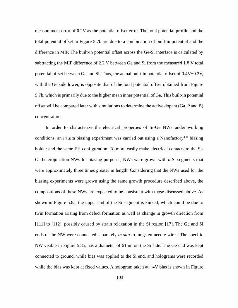
measurement error of 0.2V as the potential offset error. The total potential profile and the
total potential offset in Figure 5.7b are due to a combination of built-in potential and the
difference in MIP. The built-in potential offset across the Ge-Si interface is calculated by
subtracting the MIP difference of 2.2 V between Ge and Si from the measured 1.8 V total
potential offset between Ge and Si. Thus, the actual built-in potential offset of 0.4V±0.2V,
with the Ge side lower, is opposite that of the total potential offset obtained from Figure
5.7b, which is primarily due to the higher mean inner potential of Ge. This built-in potential
offset will be compared later with simulations to determine the active dopant (Ga, P and B)
concentrations.
In order to characterize the electrical properties of Si-Ge NWs under working
conditions, an in situ biasing experiment was carried out using a NanofactoryTM biasing
holder and the same EH configuration. To more easily make electrical contacts to the Si-
Ge heterojunction NWs for biasing purposes, NWs were grown with n-Si segments that
were approximately three times greater in length. Considering that the NWs used for the
biasing experiments were grown using the same growth procedure described above, the
compositions of these NWs are expected to be consistent with those discussed above. As
shown in Figure 5.8a, the upper end of the Si segment is kinked, which could be due to
twin formation arising from defect formation as well as change in growth direction from
[111] to [112], possibly caused by strain relaxation in the Si region [17]. The Ge and Si
ends of the NW were connected separately in situ to tungsten needle wires. The specific
NW visible in Figure 5.8a, has a diameter of 61nm on the Si side. The Ge end was kept
connected to ground, while bias was applied to the Si end, and holograms were recorded
while the bias was kept at fixed values. A hologram taken at +4V bias is shown in Figure
103
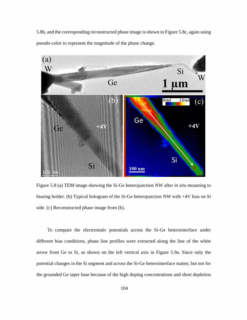
5.8b, and the corresponding reconstructed phase image is shown in Figure 5.8c, again using
pseudo-color to represent the magnitude of the phase change.
Figure 5.8 (a) TEM image showing the Si-Ge heterojunction NW after in situ mounting to
biasing holder. (b) Typical hologram of the Si-Ge heterojunction NW with +4V bias on Si
side. (c) Reconstructed phase image from (b).
To compare the electrostatic potentials across the Si-Ge heterointerface under
different bias conditions, phase line profiles were extracted along the line of the white
arrow from Ge to Si, as shown on the left vertical axis in Figure 5.9a. Since only the
potential changes in the Si segment and across the Si-Ge heterointerface matter, but not for
the grounded Ge taper base because of the high doping concentrations and short depletion
104
region, these phase profiles were divided by the width of the Si segment (61nm) and CE,
and then converted to potential, as also shown in Figure 5.9a, using the right vertical axis
for reference. The bias conditions are shown in the legend. In Figure 5.9a, the potentials
on the Ge side under different bias conditions are very similar because the Ge end is
connected to ground. The linear change of phase and potential on the Ge side is caused by
the tapered Ge NW shape which is not considered here. On the Si side, the potential is
observed to increase in proportion to an increase in bias for applied positive voltage. For
example, the potential on Si side increases by 5V, when +5 V bias is applied to the NW.
The slope of potential change near the SiGe heterointerface also increases as the positive
bias is increased. However, when negative bias is applied, the potential on the Si side
decreases only slightly as the bias becomes more negative, although the slope change is
not obvious. The dip in potential at ~250 nm is caused by the difference in MIP between
Ge, Si and mixed region, offset by the built-in potential. When positive bias is applied, the
bottom of the dip and the nearby mixed interface region and Ge segment also increase by
small amounts as the bias increases, whereas this area remains almost constant when
negative bias is applied. The slight bending in the potential and phase profiles is similar
under different bias conditions and could be caused by small bending of the NW in the Si
segment and/or diffraction effects, which can be seen in the darker contrast of Si in Figure
5.8b.
The corresponding current−voltage (I-V) characteristic curve measurement is shown
in Figure 5.9b. When positive bias is applied to Si, the I-V curve shows a rectifying effect
and the current starts to increase rapidly when the bias exceeds ~2 V. When negative bias
is applied, the current starts to increase when the bias is greater than ~-2V and the I-V curve
105
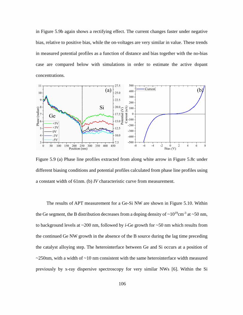
in Figure 5.9b again shows a rectifying effect. The current changes faster under negative
bias, relative to positive bias, while the on-voltages are very similar in value. These trends
in measured potential profiles as a function of distance and bias together with the no-bias
case are compared below with simulations in order to estimate the active dopant
concentrations.
Figure 5.9 (a) Phase line profiles extracted from along white arrow in Figure 5.8c under
different biasing conditions and potential profiles calculated from phase line profiles using
a constant width of 61nm. (b) IV characteristic curve from measurement.
The results of APT measurement for a Ge-Si NW are shown in Figure 5.10. Within
the Ge segment, the B distribution decreases from a doping density of ~1019cm-3 at ~50 nm,
to background levels at ~200 nm, followed by i-Ge growth for ~50 nm which results from
the continued Ge NW growth in the absence of the B source during the lag time preceding
the catalyst alloying step. The heterointerface between Ge and Si occurs at a position of
~250nm, with a width of ~10 nm consistent with the same heterointerface width measured
previously by x-ray dispersive spectroscopy for very similar NWs [6]. Within the Si
106
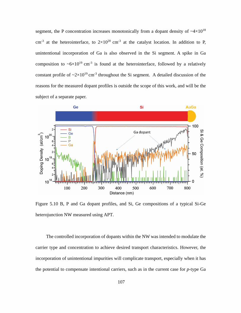
segment, the P concentration increases monotonically from a dopant density of ~4×10¹⁸
cm-3 at the heterointerface, to 2×1020 cm-3 at the catalyst location. In addition to P,
unintentional incorporation of Ga is also observed in the Si segment. A spike in Ga
composition to ~6×1019 cm-3 is found at the heterointerface, followed by a relatively
constant profile of ~2×1019 cm-3 throughout the Si segment. A detailed discussion of the
reasons for the measured dopant profiles is outside the scope of this work, and will be the
subject of a separate paper.
Figure 5.10 B, P and Ga dopant profiles, and Si, Ge compositions of a typical Si-Ge
heterojunction NW measured using APT.
The controlled incorporation of dopants within the NW was intended to modulate the
carrier type and concentration to achieve desired transport characteristics. However, the
incorporation of unintentional impurities will complicate transport, especially when it has
the potential to compensate intentional carriers, such as in the current case for p-type Ga
107
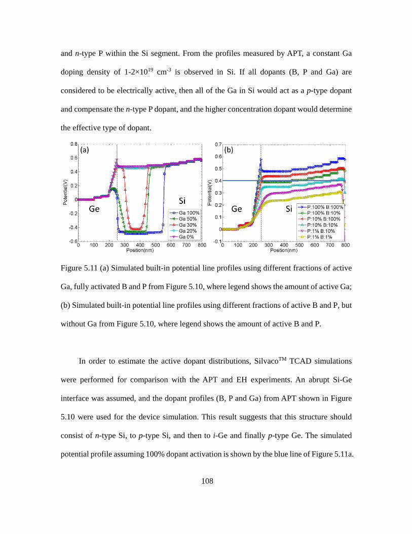
and n-type P within the Si segment. From the profiles measured by APT, a constant Ga
doping density of 1-2×1019 cm-3 is observed in Si. If all dopants (B, P and Ga) are
considered to be electrically active, then all of the Ga in Si would act as a p-type dopant
and compensate the n-type P dopant, and the higher concentration dopant would determine
the effective type of dopant.
Figure 5.11 (a) Simulated built-in potential line profiles using different fractions of active
Ga, fully activated B and P from Figure 5.10, where legend shows the amount of active Ga;
(b) Simulated built-in potential line profiles using different fractions of active B and P, but
without Ga from Figure 5.10, where legend shows the amount of active B and P.
In order to estimate the active dopant distributions, SilvacoTM TCAD simulations
were performed for comparison with the APT and EH experiments. An abrupt Si-Ge
interface was assumed, and the dopant profiles (B, P and Ga) from APT shown in Figure
5.10 were used for the device simulation. This result suggests that this structure should
consist of n-type Si, to p-type Si, and then to i-Ge and finally p-type Ge. The simulated
potential profile assuming 100% dopant activation is shown by the blue line of Figure 5.11a.
108
The built-in potential of the n-type Si would be ~0.5V (at ~600nm), while the potential of
the p-type Si would be ~-0.4V (at ~400nm), relative to Ge (at ~0nm). Thus, this dopant
profile would result in a potential drop of ~0.9V in Si from the n-type segment to the p-
type segment and another 0.4V potential step across the SiGe interface with the Ge side
being higher. The slow potential decrease in Si from 600nm to ~800nm is caused by the P
dopant concentration decrease.
The unintentional Ga dopant in the Si part of the NW might incorporate interstitially,
or it could form Ga-vacancy defects or other small defect clusters and not be fully activated.
Thus, simulations with partially activated Ga are also shown in Figure 5.11a, where the
legend shows the fraction of activated Ga. With lower active Ga concentrations, the p-type
segment length in Si is reduced, while the potential offset between n-type Si and p-type Si
decreases slightly (less than 0.1V from 100% to 30%). When the active Ga is reduced to
concentrations lower than that of P (~20% of Ga dopant), the p-type Si segment disappears
and only one potential drop of ~0.5V is visible within Ge at ~250nm, effectively forming
an nip-like Si-Ge heterojunction. The experimental EH result from Figure 5.7b indicated
that the built-in potential had 0.4V offset across the Si-Ge interface and the potential for
the Ge side was always lower than for Si. Moreover, if there is a p-type Si segment, either
the Si-Ge heterointerface or the np junction in the Si segment would always be in reverse
bias and the current should be small until the junction breaks down. This situation is not
consistent with the I-V curve measurements, as shown in Figure 5.9b. These comparisons
suggest that the Ga is less than 20% activated. According to the literature [23], the solubility
of Ga in Si is lower than 1×1019 cm-3. Also, Ga dopants in Si have only been reported to be
active up to ~1018 cm-3 with only partial activation at higher concentrations due to the
109
relatively high activation energy [24-26]. Therefore, we conclude that only a small fraction
of the Ga atoms present are activated at most, and since the active Ga concentration must
be lower than that of the active P, its influence can be included in the simulations below
by the active P level.
In order to determine the activation of the P and B dopants, the built-in potentials
across the Si-Ge heterojunction were simulated using varying amounts of active P and B,
as shown in Figure 5.11b. These simulations show that the built-in potential offset between
Si and Ge is ~0.48V (at ~400nm relative to Ge at 0nm), with the Ge side lower, if both P
and B are fully activated (100% P and 100% B). If the active B is 100% and P is only 10%,
then the potential offset is reduced to 0.44V and if the active B is only 10% and P is 100%,
then the potential offset is 0.39V. Further reductions of the active P and B concentrations
by an order of magnitude did not affect the built-in potential offset by very much. Moreover,
most of the depletion and built-in potential change across the Si-Ge heterojunction
remained in the region from 200 nm to 250 nm so that the length of the depletion region
stayed at about the same size as the i-Ge segment (~50 nm). Since most of the built-in
potential increase from Ge to Si is in the i-Ge region, from 200 nm to 250 nm, a phase
increase in the Ge segment right before the Si-Ge interface would be expected at ~400nm
in Figure 5.7b. However, this signal was not observed in the experiment, possibly because
of the complexity of the SiGe interface and differences in MIP discussed above. The built-
in potential offset measured from the holography experiment was ~0.4±0.2 V, which
closely fitted the cases simulated for 10% B in Ge and 100% P in Si, and for 100% B in Ge
and 10% P in Si. However, the potential profile from the holography experiments was noisy
because of the NW surface irregularities and cannot readily distinguish the ~0.2 V
110
difference. Therefore, the amount of active P and B dopants cannot be accurately
determined under these experimental conditions, and it can only be concluded that either
100% active P and 10% B, or 10% P and 100% B give the closest fit between experiment
and simulations. A further comparison with simulation under biasing conditions is most
likely needed to determine the active dopant concentrations.
In Figure 5.7b, the total change of potential in the Si segment from 500nm to 650nm
is ~0.7 V, whereas the change of Si NW width, measured from the width profile in Figure
5.7a and 5.6d, is only 3%, which would only cause about 0.3 V difference. Moreover, the
potential in the Si segment extending from 450nm to 800nm in Figure 5.11b increases by
0.1 V because the dopant level increases close to the catalyst. Au has been reported to form
a Schottky contact with Si [13]. However, because the P dopant concentration near the
catalyst is so high, the built-in potential change due to the Schottky contact is limited to a
very small area adjacent to the catalyst and should not influence measurements across the
Si-Ge heterojunction, as shown at ~800nm in Figure 5.11b. Thus, the increase of potential
from 550nm to 650nm in Figure 5.7b can be partially explained by the combined effect of
diameter increase and P dopant concentration increase. The extra potential offset could be
due to diffraction near the catalyst.
111
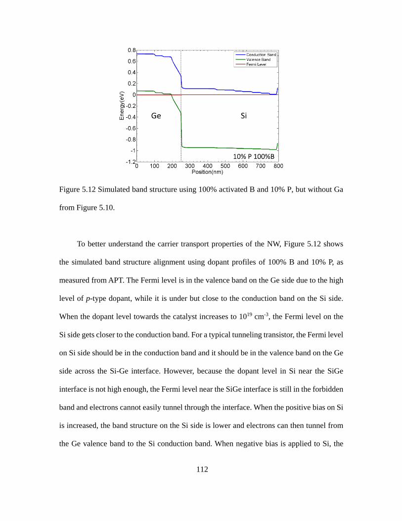
Figure 5.12 Simulated band structure using 100% activated B and 10% P, but without Ga
from Figure 5.10.
To better understand the carrier transport properties of the NW, Figure 5.12 shows
the simulated band structure alignment using dopant profiles of 100% B and 10% P, as
measured from APT. The Fermi level is in the valence band on the Ge side due to the high
level of p-type dopant, while it is under but close to the conduction band on the Si side.
When the dopant level towards the catalyst increases to 1019 cm-3, the Fermi level on the
Si side gets closer to the conduction band. For a typical tunneling transistor, the Fermi level
on Si side should be in the conduction band and it should be in the valence band on the Ge
side across the Si-Ge interface. However, because the dopant level in Si near the SiGe
interface is not high enough, the Fermi level near the SiGe interface is still in the forbidden
band and electrons cannot easily tunnel through the interface. When the positive bias on Si
is increased, the band structure on the Si side is lower and electrons can then tunnel from
the Ge valence band to the Si conduction band. When negative bias is applied to Si, the
112
band structure on the Si side is higher so that electrons can move easily from the Si
conduction band to the Ge conduction band.
In order to interpret the in situ EH biasing experiments, further simulations were done
for a similar device structure, connecting the Si end to tungsten, forming a Schottky contact,
and connecting Ge to an ohmic contact. Bias from -5V to +5V was then applied on the Si
side, with the Ge side kept grounded. The simulated built-in potential profiles under bias
are shown in Figures 5.13a and 5.13b, where Figure 5.13a uses active dopants of 100% P
and 10% B, as measured from the APT results, and Figure 5.13b uses active dopants of 10%
P and 100% B. In both cases, the simulated built-in potential offset increases as the applied
positive bias increases, whereas it only decreases slightly under different negative bias. The
built-in potential of the Ge intrinsic region increases to a smaller amount as positive bias
is applied, whereas it only decreases slightly as negative bias is applied, which would cause
the change of dip observed in Figure 5.9a. The slope in potential, moving from Ge (200
nm) to Si (250 nm), also increases under positive bias, whereas the slope of the potential
decreases slightly under negative bias. Moreover, the depletion region and built-in potential
change under negative bias is mostly distributed in the i-Ge region, from 200nm to 250nm.
However, the distribution of depletion region and built-in potential change between the two
cases is different under positive bias. In Figure 5.13a, because of the high dopant
concentration of P in Si and relatively low concentration of B in Ge, most of the depletion
region and built-in potential change is in part of the p-type Ge region and the i-Ge region,
from 120 nm to 250 nm. There is only a very small built-in potential change region located
at the n-type Si segment, from 250 to 270nm. On the other hand, in Figure 5.13b, there is
a relative low concentration of P in Si and high concentration of B in Ge. The depletion
113
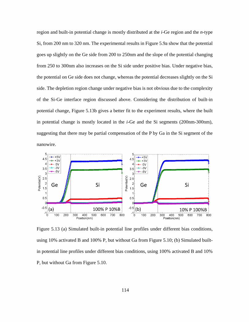
region and built-in potential change is mostly distributed at the i-Ge region and the n-type
Si, from 200 nm to 320 nm. The experimental results in Figure 5.9a show that the potential
goes up slightly on the Ge side from 200 to 250nm and the slope of the potential changing
from 250 to 300nm also increases on the Si side under positive bias. Under negative bias,
the potential on Ge side does not change, whereas the potential decreases slightly on the Si
side. The depletion region change under negative bias is not obvious due to the complexity
of the Si-Ge interface region discussed above. Considering the distribution of built-in
potential change, Figure 5.13b gives a better fit to the experiment results, where the built
in potential change is mostly located in the i-Ge and the Si segments (200nm-300nm),
suggesting that there may be partial compensation of the P by Ga in the Si segment of the
nanowire.
Figure 5.13 (a) Simulated built-in potential line profiles under different bias conditions,
using 10% activated B and 100% P, but without Ga from Figure 5.10; (b) Simulated built-
in potential line profiles under different bias conditions, using 100% activated B and 10%
P, but without Ga from Figure 5.10.
114
With positive bias applied, the Schottky contact is in forward bias and has low
resistance, while the Si-Ge heterojunction is in reverse bias and has high resistance. Thus,
most of the positive voltage would be distributed across the Si-Ge heterojunction. The
built-in potential offset across the heterojunction will increase as the bias increases. When
the bias exceeds a certain value, the Si conduction band will become low enough. Thus,
electrons from the Ge valence band can tunnel through the Si-Ge interface into the Si
conduction band, giving a rectifying effect in the IV curve, as shown in Figure 5.9b. With
negative bias, the Schottky contact is in reverse bias and has high resistance, while the Si-
Ge heterojunction is in forward bias. The resistance of the heterojunction is low compared
to the Schottky and ohmic contacts, and most of the negative voltage is distributed on the
contacts. Therefore, the built-in potential offset across the heterojunction will be close to
the one without bias and will not change much under different negative bias. Due to the
high dopant level in Si near the catalyst, electrons can tunnel through the Schottky contact
and thus there is still a rectifying effect due to the Si-Ge heterojunction, which is visible in
the IV curve in Figure 5.9b. Therefore, the change of dip and nearby Ge segment, as well
as the Si segment in Figure 5.9a, can be explained and the simulation results match well
with the in situ holography biasing experiment.
5.4 Conclusions
Doped Si-Ge heterojunction NWs have been grown using the VLS method, and APT
measurements were made to extract the B, P and Ga dopant concentrations as well as the
Si, Ge composition profiles. The electrostatic potential profile measured by electron
holography showed that the total potential offset across the Si-Ge heterojunction had the
115
value of 1.8±0.2V, with the Si side lower, whereas the built-in potential offset had the value
of 0.4±0.2V, with the Ge side lower because of the difference in MIP between Ge and Si.
Comparisons with simulations indicated that the Ga present in the Si region was, at most,
only partially activated and that its effect could be ignored. The P and B active dopants
could not be determined accurately due to noise from the irregular NW surface and
insensitivity in the depletion region length because of the i-Ge region. In situ biasing
experiments combined with electron holography were also performed. With positive bias
on Si, most of the voltage was distributed across the Si-Ge heterojunction and its built-in
potential increased to the same amount as the applied bias, whereas most of the voltage
was distributed on the contacts with negative bias on Si and the built-in potential across
the heterojunction was not changed much. Comparisons between biasing EH results and
simulations indicated that the B dopant in Ge is mostly activated but not the P dopant in Si,
possibly due to partial compensation by Ga in the Si region. The I−V characteristic curve
was measured and could also be explained using simulations. Overall, these results
demonstrated that off-axis electron holography, APT and TCAD simulations provide a
powerful combination for understanding the electrically active dopant distributions in
doped NW device heterostructures.
116
References
[1] Z. Gan, D. Perea, J. Yoo, Y. He, R. Colby, B. Barker, M. Gu, S. Mao, C. Wang, S. Tom Picraux, D. Smith, and M. McCartney, Unpublished (2015).
[2] M. S. Gudiksen, L. J. Lauhon, J. Wang, D. C. Smith, and C. M. Lieber, Nature 415 617 (2002).
[3] S. M. Sze, Physics of semiconductor devices, 2nd ed. Wiley, New York, (1981).
[4] V. Schmidt, H. Riel, S. Senz, S. Karg, W. Riess, and U. Gosele, Small 2 85 (2006).
[5] J. Goldberger, A. I. Hochbaum, R. Fan, and P. Yang, Nano letters 6 973 (2006).
[6] D. E. Perea, N. Li, R. M. Dickerson, A. Misra, and S. T. Picraux, Nano letters 11 3117 (2011).
[7] C. Y. Wen, M. C. Reuter, J. Bruley, J. Tersoff, S. Kodambaka, E. A. Stach, and F. M. Ross, Science 326 1247 (2009).
[8] L. Chen, W. Y. Fung, and W. Lu, Nano letters 13 5521 (2013).
[9] D. E. Perea, E. Wijaya, J. L. Lensch-Falk, E. R. Hemesath, and L. J. Lauhon, Journal of Solid State Chemistry 181 1642 (2008).
[10] D. E. Perea, E. R. Hemesath, E. J. Schwalbach, J. L. Lensch-Falk, P. W. Voorhees, and L. J. Lauhon, Nature nanotechnology 4 315 (2009).
[11] M. R. McCartney and D. J. Smith, Annual Review of Materials Research 37 729 (2007).
[12] M. R. McCartney, N. Agarwal, S. Chung, D. A. Cullen, M.-G. Han, K. He, L. Li, H. Wang, L. Zhou, and D. J. Smith, Ultramicroscopy 110 375 (2010).
[13] Z. Gan, D. E. Perea, J. Yoo, S. Tom Picraux, D. J. Smith, and M. R. McCartney, Applied Physics Letters 103 153108 (2013).
[14] L. Li, Z. Gan, M. R. McCartney, H. Liang, H. Yu, W. J. Yin, Y. Yan, Y. Gao, J. Wang, and D. J. Smith, Adv Mater 26 1052 (2014).
[15] M. I. den Hertog, H. Schmid, D. Cooper, J. L. Rouviere, M. T. Bjork, H. Riel, P. Rivallin, S. Karg, and W. Riess, Nano letters 9 3837 (2009).
[16] N. Li, T. Y. Tan, and U. Gösele, Applied Physics A 90 591 (2008).
[17] S. A. Dayeh, J. Wang, N. Li, J. Y. Huang, A. V. Gin, and S. T. Picraux, Nano letters 11 4200 (2011).
117
[18] S. A. Dayeh, N. H. Mack, J. Y. Huang, and S. T. Picraux, Applied Physics Letters 99 023102 (2011).
[19] J. E. Allen, E. R. Hemesath, D. E. Perea, J. L. Lensch-Falk, Z. Y. Li, F. Yin, M. H. Gass, P. Wang, A. L. Bleloch, R. E. Palmer, and L. J. Lauhon, Nature nanotechnology 3 168 (2008).
[20] M. J. Hytch, E. Snoeck, and R. Kilaas, Ultramicroscopy 74 131 (1998).
[21] J. Li, M. R. McCartney, R. E. Dunin-Borkowski, and D. J. Smith, Acta Crystallographica Section A 55 652 (1999).
[22] J. Li, M. R. McCartney, and D. J. Smith, Ultramicroscopy 94 149 (2003).
[23] F. A. Trumbore, Bell System Technical Journal 39 205 (1960).
[24] T. Hoshikawa, X. Huang, K. Hoshikawa, and S. Uda, Japanese Journal of Applied Physics 47 8691 (2008).
[25] K. B. Wolfstirn, Journal of Physics and Chemistry of Solids 16 279 (1960).
[26] N. Sclar, Electron Devices, IEEE Transactions on 24 709 (1977).
118
CHAPTER 6
CHARACTERIZATION OF TRAPPED CHARGES IN Ge/LixGe CORE/SHELL
STRUCTURE DURING LITHIATION USING OFF-AXIS ELECTRON
HOLOGRAPHY
This chapter describes the lithiation of Ge nanowires (NWs) and the measurement of
trapped charges in Ge/LixGe core/shell NWs using off-axis electron holography. The Ge
NWs were grown using the vapor-liquid-solid (VLS) method, and were provided by
Chongmin Wang and Meng Gu from Pacific Northwest National Laboratory. My
contribution to this work has included characterization of the NW lithiation process,
measurement of electrostatic profiles across the core/shell structures, and simulations for
estimation of the trapped charge.
6.1 Introduction
Lithium ion batteries (LIBs) have important applications as energy-storage systems
for portable electronics, electric vehicles, and sources of renewable energy such as wind
and solar [1,2]. Graphite is currently used as the anode material in commercial LIBs.
However, graphite has a limited theoretical capacity of 372 mAhg-1 and it cannot meet the
growing demands for high energy density and long life-time [3,4]. Novel materials such as
other group IV materials (Si, Ge and Sn), with higher theoretical capacities, are being
considered as possible alternatives [3]. Si has received most attention because of its greatest
theoretical capacity of 3579 mAhg-1 and 8334AhL-1 for Li15Si4 at room temperature, as
well as its abundance [5,6]. Relative to Si, Ge has lower theoretical capacities of 1384
119
mAhg-1 and 7366 AhL-1 for Li15Ge4 at room temperature, and it is more expensive [3,7].
However, Ge has higher intrinsic electronic conductivity because of its smaller band gap
(0.6eV) compared to Si (1.1eV) [8]. Moreover, the Li ion diffusivity in Ge is about two
times larger, compared to Si [9,10]. Thus, Ge has high charging/discharging rates in LIBs,
compared to Si, which is also an important consideration for LIB applications. Despite
these advantages, a major drawback of using Si or Ge is the huge volume change upon full
lithiation/delithiation (281% for Si and 246% for Ge), which may lead to degradation of
electrodes and the solid electrolyte interface (SEI), causing irreversible loss of LIB capacity
[11-15]. Nanostructures have been developed to accommodate the strain during lithiation
and to increase rate capability by shortening the Li ion diffusion length [16-18].
In situ transmission electron microscopy (TEM) has been used to characterize the
microstructure and phase transition behavior during lithiation/delithiation for several
materials, including Si, Ge and Sn, by using open cell structures with liquid or solid
electrolytes [11,14,19-23]. Two-step phase transformation: c-Ge(Si)→a-LixGe(LixSi)→c-
Li15Ge4(Li15Si4) has been observed during Ge (Si) lithiation [11,20,22]. Anisotropic
lithiation was observed for different growth directions in Si, whereas isotropic lithiation
was observed in Ge [11,14]. Amorphous LixGe(Si) and crystal Ge(Si) interfaces have been
studied during lithiation to understand the lithiation mechanism with atomic-scale
resolution [19,21,24]. Simulations have also been performed to prove that extra electrons
in Si near the LixSi-Si interface drive the solid-state amorphization of Li-Si alloy [25].
Knowledge of the charge distribution during lithiation is important for developing a better
understanding of the lithiation mechanism and the associated electrochemistry. Off-axis
120
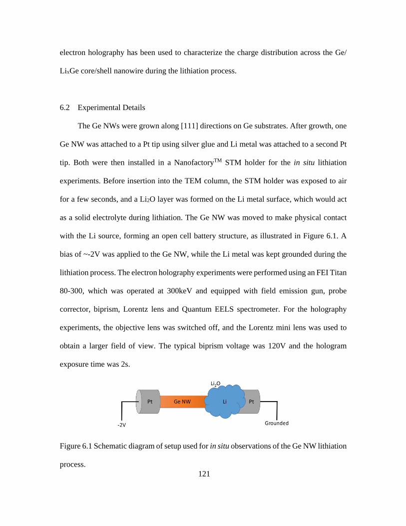
electron holography has been used to characterize the charge distribution across the Ge/
LixGe core/shell nanowire during the lithiation process.
6.2 Experimental Details
The Ge NWs were grown along [111] directions on Ge substrates. After growth, one
Ge NW was attached to a Pt tip using silver glue and Li metal was attached to a second Pt
tip. Both were then installed in a NanofactoryTM STM holder for the in situ lithiation
experiments. Before insertion into the TEM column, the STM holder was exposed to air
for a few seconds, and a Li2O layer was formed on the Li metal surface, which would act
as a solid electrolyte during lithiation. The Ge NW was moved to make physical contact
with the Li source, forming an open cell battery structure, as illustrated in Figure 6.1. A
bias of ~-2V was applied to the Ge NW, while the Li metal was kept grounded during the
lithiation process. The electron holography experiments were performed using an FEI Titan
80-300, which was operated at 300keV and equipped with field emission gun, probe
corrector, biprism, Lorentz lens and Quantum EELS spectrometer. For the holography
experiments, the objective lens was switched off, and the Lorentz mini lens was used to
obtain a larger field of view. The typical biprism voltage was 120V and the hologram
exposure time was 2s.
Figure 6.1 Schematic diagram of setup used for in situ observations of the Ge NW lithiation
process. 121
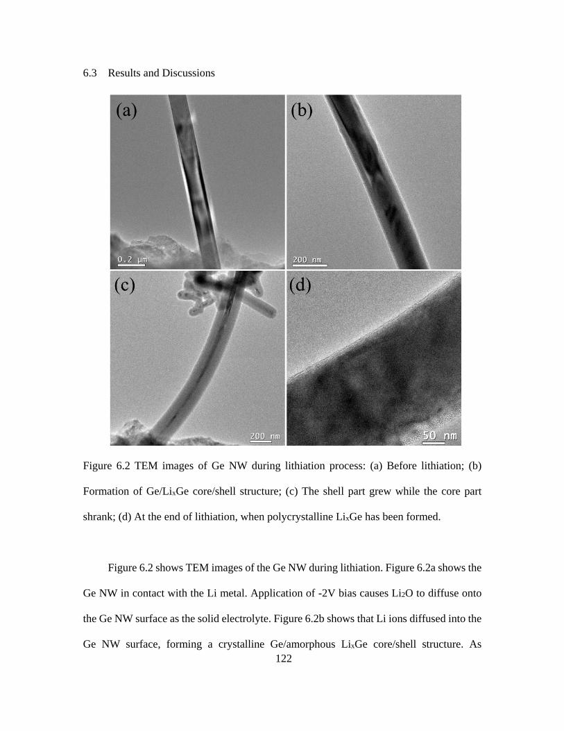
6.3 Results and Discussions
Figure 6.2 TEM images of Ge NW during lithiation process: (a) Before lithiation; (b)
Formation of Ge/LixGe core/shell structure; (c) The shell part grew while the core part
shrank; (d) At the end of lithiation, when polycrystalline LixGe has been formed.
Figure 6.2 shows TEM images of the Ge NW during lithiation. Figure 6.2a shows the
Ge NW in contact with the Li metal. Application of -2V bias causes Li2O to diffuse onto
the Ge NW surface as the solid electrolyte. Figure 6.2b shows that Li ions diffused into the
Ge NW surface, forming a crystalline Ge/amorphous LixGe core/shell structure. As 122
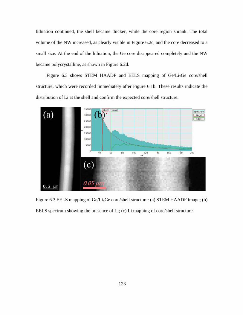
lithiation continued, the shell became thicker, while the core region shrank. The total
volume of the NW increased, as clearly visible in Figure 6.2c, and the core decreased to a
small size. At the end of the lithiation, the Ge core disappeared completely and the NW
became polycrystalline, as shown in Figure 6.2d.
Figure 6.3 shows STEM HAADF and EELS mapping of Ge/LixGe core/shell
structure, which were recorded immediately after Figure 6.1b. These results indicate the
distribution of Li at the shell and confirm the expected core/shell structure.
Figure 6.3 EELS mapping of Ge/LixGe core/shell structure: (a) STEM HAADF image; (b)
EELS spectrum showing the presence of Li; (c) Li mapping of core/shell structure.
123
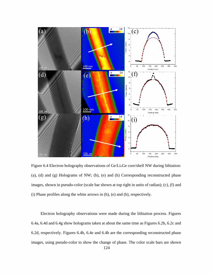
Figure 6.4 Electron holography observations of Ge/LixGe core/shell NW during lithiation:
(a), (d) and (g) Holograms of NW; (b), (e) and (h) Corresponding reconstructed phase
images, shown in pseudo-color (scale bar shown at top right in units of radian); (c), (f) and
(i) Phase profiles along the white arrows in (b), (e) and (h), respectively.
Electron holography observations were made during the lithiation process. Figures
6.4a, 6.4d and 6.4g show holograms taken at about the same time as Figures 6.2b, 6.2c and
6.2d, respectively. Figures 6.4b, 6.4e and 6.4h are the corresponding reconstructed phase
images, using pseudo-color to show the change of phase. The color scale bars are shown 124
at top right. The center part of the NW has higher phase compared to the outer parts, which
is due to the combination of greater thickness and higher mean inner potential of crystalline
Ge, compared to LixGe. Phase profiles were extracted along the white arrows in the
reconstructed phase images and shown at the right. The Ge core in Figure 6.4c is about half
the diameter of the NW, and both the core and shell parts mimic a cylindrical NW shape.
In Figure 6.4f, the Ge core has shrunk to a smaller size and it is apparently faceted, as
shown by the triangular shape at the center. The LixGe shell part has a round cross section.
In Figure 6.4h, the entire Ge NW has been lithiated, the Ge core has disappeared, and the
lithiated LixGe (x~3.75) NW again mimics a cylindrical NW shape. During this process,
the NW diameter has increased from 180nm in Figure 6.4c, to 250nm in Figure 6.4i.
The phase profiles across the NW will be caused by the mean inner potential of the
materials as well as any built-in potential. To interpret the phase profiles, it is first assumed
that there are initially no trapped charges in the NW and that the phase shift is due only to
mean inner potential Vshell and change of thickness. A model including trapped charges is
discussed further below. Assuming that the NW has a cylindrical shape, then the phase
shift due to the shell part can be calculated and compared with the experimental results, as
shown by the red curves in Figure 6.4c, 6.4f and 6.4i. From the fitting for the best fitted
Vshell, it seems that a cylindrical NW shape fits reasonably well with the experimental
results. The best fitted values of Vshell for these three stages of lithiation are shown in table
6.1. As the lithiation continued, the mean inner potential of Vshell decreased from 7.6V to
5.1V. This drop would indicate that the Li component in the shell has increased during
lithiation, because Li is a lighter element and has smaller mean inner potential, compared
to Ge. The bias applied to the NW should not affect this conclusion since the bias was kept
125
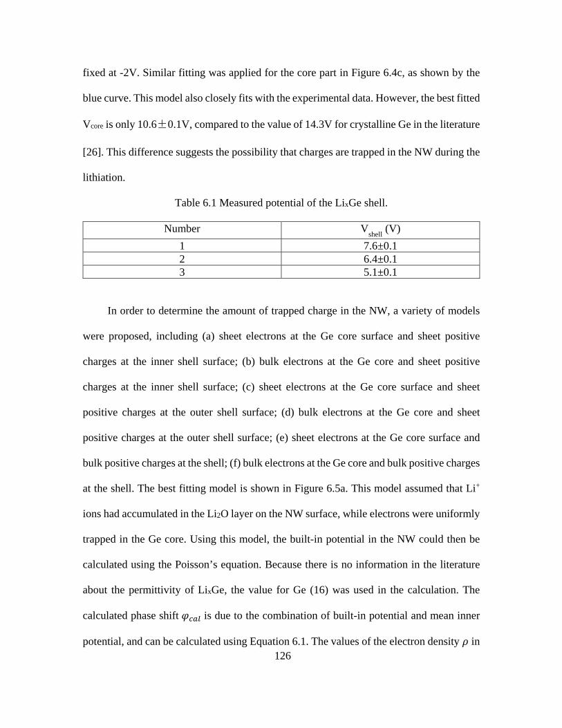
fixed at -2V. Similar fitting was applied for the core part in Figure 6.4c, as shown by the
blue curve. This model also closely fits with the experimental data. However, the best fitted
Vcore is only 10.6±0.1V, compared to the value of 14.3V for crystalline Ge in the literature
[26]. This difference suggests the possibility that charges are trapped in the NW during the
lithiation.
Table 6.1 Measured potential of the LixGe shell.
Number Vshell (V) 1 7.6±0.1 2 6.4±0.1 3 5.1±0.1
In order to determine the amount of trapped charge in the NW, a variety of models
were proposed, including (a) sheet electrons at the Ge core surface and sheet positive
charges at the inner shell surface; (b) bulk electrons at the Ge core and sheet positive
charges at the inner shell surface; (c) sheet electrons at the Ge core surface and sheet
positive charges at the outer shell surface; (d) bulk electrons at the Ge core and sheet
positive charges at the outer shell surface; (e) sheet electrons at the Ge core surface and
bulk positive charges at the shell; (f) bulk electrons at the Ge core and bulk positive charges
at the shell. The best fitting model is shown in Figure 6.5a. This model assumed that Li+
ions had accumulated in the Li2O layer on the NW surface, while electrons were uniformly
trapped in the Ge core. Using this model, the built-in potential in the NW could then be
calculated using the Poisson’s equation. Because there is no information in the literature
about the permittivity of LixGe, the value for Ge (16) was used in the calculation. The
calculated phase shift 𝑖𝑖𝑐𝑐𝑠𝑠𝑜𝑜 is due to the combination of built-in potential and mean inner
potential, and can be calculated using Equation 6.1. The values of the electron density 𝜌𝜌 in 126
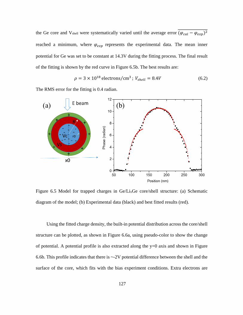
the Ge core and Vshell were systematically varied until the average error (𝑖𝑖𝑐𝑐𝑠𝑠𝑜𝑜 − 𝑖𝑖𝑒𝑒𝑚𝑚𝑠𝑠)2
reached a minimum, where 𝑖𝑖𝑒𝑒𝑚𝑚𝑠𝑠 represents the experimental data. The mean inner
potential for Ge was set to be constant at 14.3V during the fitting process. The final result
of the fitting is shown by the red curve in Figure 6.5b. The best results are:
𝜌𝜌 = 3 × 10¹⁸ electrons cm3⁄ ; 𝑉𝑉𝑠𝑠ℎ𝑒𝑒𝑜𝑜𝑜𝑜 = 8.4𝑉𝑉 (6.2)
The RMS error for the fitting is 0.4 radian.
Figure 6.5 Model for trapped charges in Ge/LixGe core/shell structure: (a) Schematic
diagram of the model; (b) Experimental data (black) and best fitted results (red).
Using the fitted charge density, the built-in potential distribution across the core/shell
structure can be plotted, as shown in Figure 6.6a, using pseudo-color to show the change
of potential. A potential profile is also extracted along the y=0 axis and shown in Figure
6.6b. This profile indicates that there is ~-2V potential difference between the shell and the
surface of the core, which fits with the bias experiment conditions. Extra electrons are
127
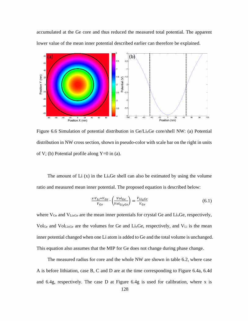
accumulated at the Ge core and thus reduced the measured total potential. The apparent
lower value of the mean inner potential described earlier can therefore be explained.
Figure 6.6 Simulation of potential distribution in Ge/LixGe core/shell NW: (a) Potential
distribution in NW cross section, shown in pseudo-color with scale bar on the right in units
of V; (b) Potential profile along Y=0 in (a).
The amount of Li (x) in the LixGe shell can also be estimated by using the volume
ratio and measured mean inner potential. The proposed equation is described below:
𝑚𝑚∙𝑉𝑉𝐿𝐿𝑖𝑖+𝑉𝑉𝐺𝐺𝑟𝑟𝑉𝑉𝐺𝐺𝑟𝑟
∙ � 𝑉𝑉𝑜𝑜𝑜𝑜𝐺𝐺𝑟𝑟𝑉𝑉𝑜𝑜𝑜𝑜𝐿𝐿𝑖𝑖𝑚𝑚𝐺𝐺𝑟𝑟
� = 𝑉𝑉𝐿𝐿𝑖𝑖𝑚𝑚𝐺𝐺𝑟𝑟𝑉𝑉𝐺𝐺𝑟𝑟
(6.1)
where VGe and VLixGe are the mean inner potentials for crystal Ge and LixGe, respectively,
VolGe and VolLixGe are the volumes for Ge and LixGe, respectively, and VLi is the mean
inner potential changed when one Li atom is added to Ge and the total volume is unchanged.
This equation also assumes that the MIP for Ge does not change during phase change.
The measured radius for core and the whole NW are shown in table 6.2, where case
A is before lithiation, case B, C and D are at the time corresponding to Figure 6.4a, 6.4d
and 6.4g, respectively. The case D at Figure 6.4g is used for calibration, where x is 128
approximated to be 3.75 for the fully lithiated phase and the volume ratio 𝑉𝑉𝑜𝑜𝑜𝑜𝐺𝐺𝑟𝑟𝑉𝑉𝑜𝑜𝑜𝑜𝐿𝐿𝑖𝑖𝑚𝑚𝐺𝐺𝑟𝑟
was
calculated to be 0.13. The value for VLi is then calculated to be 6.27V, using 14.3V MIP
for crystal Ge [26] and Equation 6.1. Since the core disappeared, there should be no trapped
charge in the NW structure, which might influence the result.
Table 6.2 Measured radius for NW core and whole NW.
Case Core (nm) Whole NW (nm) A - 66 B 45 88 C - 110 D - 129
After the calibration, the amount of Li x in LixGe can be calculated, again using
Equation 6.1. For case B at Figure 6.4a, the x in the NW shell is calculated to be 2.4 for
the measured MIP of 7.6V, where the effect of trapped charge was ignored, while x is
calculated to be 2.9 for the measured MIP of 8.4V, where effect of trapped charge was
included by using the best fitted model discussed above. These results indicate that the
intermediate lithiated state for NW shell is LixGe, where x is significantly lower than 3.75.
As the lithiation process continued, more Li might be diffused into the LixGe shell structure
and thus x was increased until it reached 3.75 and the NW was fully lithiated. The case C
cannot be calculated to confirm this result because the core is faceted and its cross section
area cannot be calculated. Further experiments and other methods might be necessary for
further investigation.
129
6.4 Conclusions
A Ge NW was lithiated in situ by applying 2V bias between its two ends, and TEM,
STEM and EELS were used to characterize the changes in the Ge/LixGe core/shell structure.
Electron holograms were taken during the lithiation process to determine the charge
distribution inside the NW. The mean inner potential for LixGe decreased during the
process, due to an increase of the Li content in the shell. Lower potential at the Ge core
was also discovered, and attributed to accumulation of trapped charge. A model was
proposed to explain the lower measured Ge potential, and the amount of trapped charge in
the Ge core was calculated to be 3×10¹⁸ electrons/cm3. The amount of Li during lithiation
was calculated using MIP and volume ratio. It suggests that the Li amount in LixGe during
lithiation might be lower than the fully lithiated phase and increased during the lithiation
process.
130
References
[1] M. Armand and J. M. Tarascon, Nature 451 652 (2008).
[2] A. S. Arico, P. Bruce, B. Scrosati, J.-M. Tarascon, and W. van Schalkwijk, Nature materials 4 366 (2005).
[3] D. Larcher, S. Beattie, M. Morcrette, K. Edstrom, J.-C. Jumas, and J.-M. Tarascon, Journal of Materials Chemistry 17 3759 (2007).
[4] Y.-M. Chiang, Science 330 1485 (2010).
[5] M. N. Obrovac and L. Christensen, Electrochemical and Solid-State Letters 7 A93 (2004).
[6] M. N. Obrovac and L. J. Krause, Journal of The Electrochemical Society 154 A103 (2007).
[7] L. Baggetto and P. H. L. Notten, Journal of The Electrochemical Society 156 A169 (2009).
[8] S. M. Sze, Physics of semiconductor devices, 2nd ed. Wiley, New York, (1981).
[9] C. Fuller and J. Severiens, Physical Review 96 21 (1954).
[10] J. Graetz, C. C. Ahn, R. Yazami, and B. Fultz, Journal of The Electrochemical Society 151 A698 (2004).
[11] X. H. Liu, Y. Liu, A. Kushima, S. Zhang, T. Zhu, J. Li, and J. Y. Huang, Advanced Energy Materials 2 722 (2012).
[12] L. Y. Beaulieu, K. W. Eberman, R. L. Turner, L. J. Krause, and J. R. Dahn, Electrochemical and Solid-State Letters 4 A137 (2001).
[13] C. K. Chan, H. Peng, G. Liu, K. McIlwrath, X. F. Zhang, R. A. Huggins, and Y. Cui, Nat Nano 3 31 (2008).
[14] X. H. Liu, H. Zheng, L. Zhong, S. Huang, K. Karki, L. Q. Zhang, Y. Liu, A. Kushima, W. T. Liang, J. W. Wang, J. H. Cho, E. Epstein, S. A. Dayeh, S. T. Picraux, T. Zhu, J. Li, J. P. Sullivan, J. Cumings, C. Wang, S. X. Mao, Z. Z. Ye, S. Zhang, and J. Y. Huang, Nano letters 11 3312 (2011).
[15] B. Key, R. Bhattacharyya, M. Morcrette, V. Seznéc, J.-M. Tarascon, and C. P. Grey, J Am Chem Soc 131 9239 (2009).
[16] P. G. Bruce, B. Scrosati, and J.-M. Tarascon, Angewandte Chemie International Edition 47 2930 (2008).
131
[17] L. Ji, Z. Lin, M. Alcoutlabi, and X. Zhang, Energy & Environmental Science 4 2682 (2011).
[18] H. Wu and Y. Cui, Nano Today 7 414 (2012).
[19] X. H. Liu, J. W. Wang, S. Huang, F. Fan, X. Huang, Y. Liu, S. Krylyuk, J. Yoo, S. A. Dayeh, A. V. Davydov, S. X. Mao, S. T. Picraux, S. Zhang, J. Li, T. Zhu, and J. Y. Huang, Nature nanotechnology 7 749 (2012).
[20] X. H. Liu, L. Q. Zhang, L. Zhong, Y. Liu, H. Zheng, J. W. Wang, J. H. Cho, S. A. Dayeh, S. T. Picraux, J. P. Sullivan, S. X. Mao, Z. Z. Ye, and J. Y. Huang, Nano letters 11 2251 (2011).
[21] Y. Liu, X. H. Liu, B. M. Nguyen, J. Yoo, J. P. Sullivan, S. T. Picraux, J. Y. Huang, and S. A. Dayeh, Nano letters 13 4876 (2013).
[22] X. H. Liu and J. Y. Huang, Energy & Environmental Science 4 3844 (2011).
[23] X. H. Liu, S. Huang, S. T. Picraux, J. Li, T. Zhu, and J. Y. Huang, Nano letters 11 3991 (2011).
[24] Y. Liu, S. Zhang, and T. Zhu, ChemElectroChem 1 706 (2014).
[25] M. Gu, H. Yang, D. E. Perea, J. G. Zhang, S. Zhang, and C. M. Wang, Nano letters 14 4622 (2014).
[26] J. Li, M. R. McCartney, R. E. Dunin-Borkowski, and D. J. Smith, Acta Crystallographica Section A 55 652 (1999).
132
CHAPTER 7
SUMMARY AND FUTURE WORK
7.1 Summary
The research of this dissertation has involved quantitative analysis of electrostatic
potential profiles and charge distributions in semiconductor nanostructures using off-axis
electron holography.
ZnO nanowires (NWs) and thin films have been investigated. The mean inner
potential (MIP) and inelastic mean free path (IMFP) of ZnO has been measured using ZnO
NWs. The MIP at 200keV was measured to be 15.3V±0.2V and the IMFP was measured
to be 55±3nm. The measured MIP agreed closely with the value reported in the literature.
The MIP and IMFP values were then used to measure the thickness of a ZnO nano-sheet
and gave consistent results for thicknesses in the range of 14nm-18nm.
ZnTe thin films have also been studied. The MIP was measured using intrinsic ZnTe
thin films and convergent beam electron diffraction (CBED). The MIP at 200keV was
measured to be 13.7±0.6V and the IMFP was measured to be 46±2nm. The MIP
measurement matched the value obtained by calculations. The measured MIP and IMFP
were then used to study a ZnTe thin film expected to have a p-n junction. However, no
change in signal due to built-in potential was observed across a junction. Possible reasons
might be: (a) the Al dopants were not activated; or (b) the junction was outside the field of
view of the holography experiment. Dynamical effects were systematically studied using
Bloch wave simulations. Thinner samples, avoiding low-index zone axes and careful
sample tilting will all help to minimize these effects.
133
Si NWs with axial p-n junctions and Schottky junction were investigated [1]. The
Schottky junctions were formed at the end of the NW due to the presence of Au catalyst
particles. The electrostatic potential profile measured by electron holography showed that
the built-in potentials across the p-n junction and the Schottky junction, had values of
1.0±0.3V and 0.5±0.3V, respectively. Simulations indicated that the dopant concentrations
were ~1019cm-3 for donors and ~1017 cm-3 for acceptors. The positively charged Au particle
at the end of the grounded NW had to be considered in order to account for the lower work
function in the simulation. The effects of a possible transition region forming an n+-n--p
junction, and possible surface charge, were also systematically studied using simulations.
Doped Si-Ge heterojunction NWs were investigated using off-axis electron
holography, while atom probe tomography (APT) measurements were made to extract the
B, P and Ga dopant concentrations as well as the Si, Ge composition profiles [2]. The
electrostatic potential profile measured by holography showed that the total potential offset
across the Si-Ge heterojunction had the value of 1.8±0.2V, with the Si side lower, whereas
the built-in potential offset had the value of 0.4±0.2V, with the Ge side lower because of
the difference in MIP between Ge and Si. Comparisons with simulations indicated that the
Ga dopant present in the Si was, at most, only partially activated and that its effect could
be ignored. The P and B active dopants could not be determined accurately due to noise
from the irregular NW surface and insensitivity in the depletion region length because of
the i-Ge region. In situ biasing experiments combined with electron holography were also
performed. With positive bias on Si, most voltage was distributed across the Si-Ge
heterojunction and its built-in potential increased to the same amount as the applied bias,
whereas most of the voltage was distributed on the contacts with negative bias on Si and
134
the built-in potential across the heterojunction was not much changed. Comparisons
between EH biasing results and simulations indicated that the B dopant in Ge was mostly
activated but not the P dopant in Si, possibly due to partial compensation by Ga in the Si
region. The I−V characteristic curve was measured and could also be explained using
simulations.
Ge/LixGe core/shell structures were studied during lithiation using S/TEM, EELS and
holography. The Ge NW was lithiated in situ by applying 2V bias between the two ends.
Electron holograms were taken during the lithiation process to determine the charge
distribution inside the NW. The MIP for LixGe decreased during the process, due to an
increase of the Li content in the shell. Lower potential at the Ge core was also discovered,
and attributed to accumulation of trapped charge. A model was proposed to explain the
lower measured Ge potential, and the amount of trapped electrons in the Ge core was
calculated to be 3×10¹⁸ electrons/cm3. The amount of Li during lithiation was calculated
using MIP values and the volume ratio. The results suggest that the amount of Li in LixGe
during lithiation might be lower than the fully lithiated phase but increased during the
lithiation process.
Overall, this dissertation research has reiterated that off-axis electron holography is
an effective technique for quantitative characterization of nanostructure thickness and
electrostatic potential profiles with nanoscale resolution. Combining electron holography
and simulations provides information about electrically active dopant and trapped charge
distributions in semiconductor nanostructures, which are important for understanding
electrical mechanisms and for developing future semiconductor devices. Moreover,
electron holography coupled with in situ biasing can be used to characterize devices under
135
working conditions and to extract information which is not shown under unbiased
conditions.
7.2 Remarks on Possible Future Work
This dissertation research has clearly demonstrated that electron holography is an
effective technique for quantitative characterization of built-in potential, and active dopants,
as well as trapped charges, with nanoscale resolution. However, electron holography only
gives two-dimensional projected-phase information about the sample. Uniform
composition and built-in potential distributions in the sample along the electron beam
direction were assumed in this dissertation research for calculations of active dopant
concentration. For semiconductor devices, the built-in potential may vary along the beam
direction due to surface effects or inhomogeneous dopant distributions. Therefore, it is
important to obtain three-dimensional phase information and hence the built-in potential
distribution in order to make accurate measurements of dopant amounts.
This problem can be solved by taking holograms at different tilt angles and using
tomographic reconstruction [3]. 3-D holography characterization of Si thin films with p-n
junctions has been reported [4], and it was found that the surface active dopant
concentrations were lower, whereas the central ones were very close, compared to bulk
material. NWs have a large surface-to-volume ratio and the surface may play an important
role in overall dopant distributions. A preliminary tomography experiment has been
performed on Si-Ge axial heterojunction NWs using HAADF STEM tilt image series, as
shown in Figure 7.1. The tilt series were taken using FEI Titan G2 80-300 operated at
300kV. The sample was tilted from -70˚ to 70˚ and the HAADF images were taken every
136
2˚. Figure 7.1a shows a typical image that was taken at 0˚ tilt angle. The intensity from
HAADF image is directly related to the atomic number and thickness of the sample, and
therefore it satisfies the tomography reconstruction requirements. The data was
reconstructed by INSPECT3DTM using the simultaneous iterative reconstruction technique
(SIRT) algorithm with 20 iterations. The result is shown in Figure 7.1b, using pseudo-color
to show the change of intensity, and the cross section of the NW is shown in Figure 7.1c.
From the HAADF image tomography reconstruction, the composition distribution is
almost uniform in cross section and the NW grown along <111> direction has a hexagonal
cross section. However, the HAADF image is not sensitive to the dopant concentrations
nor the built-in potential. Further tomographic holography experiments are necessary so
that the three-dimensional phase as well as the built-in potential distribution can be
extracted. The active dopants in all three dimensions could thus be determined by
comparison with simulations.
137
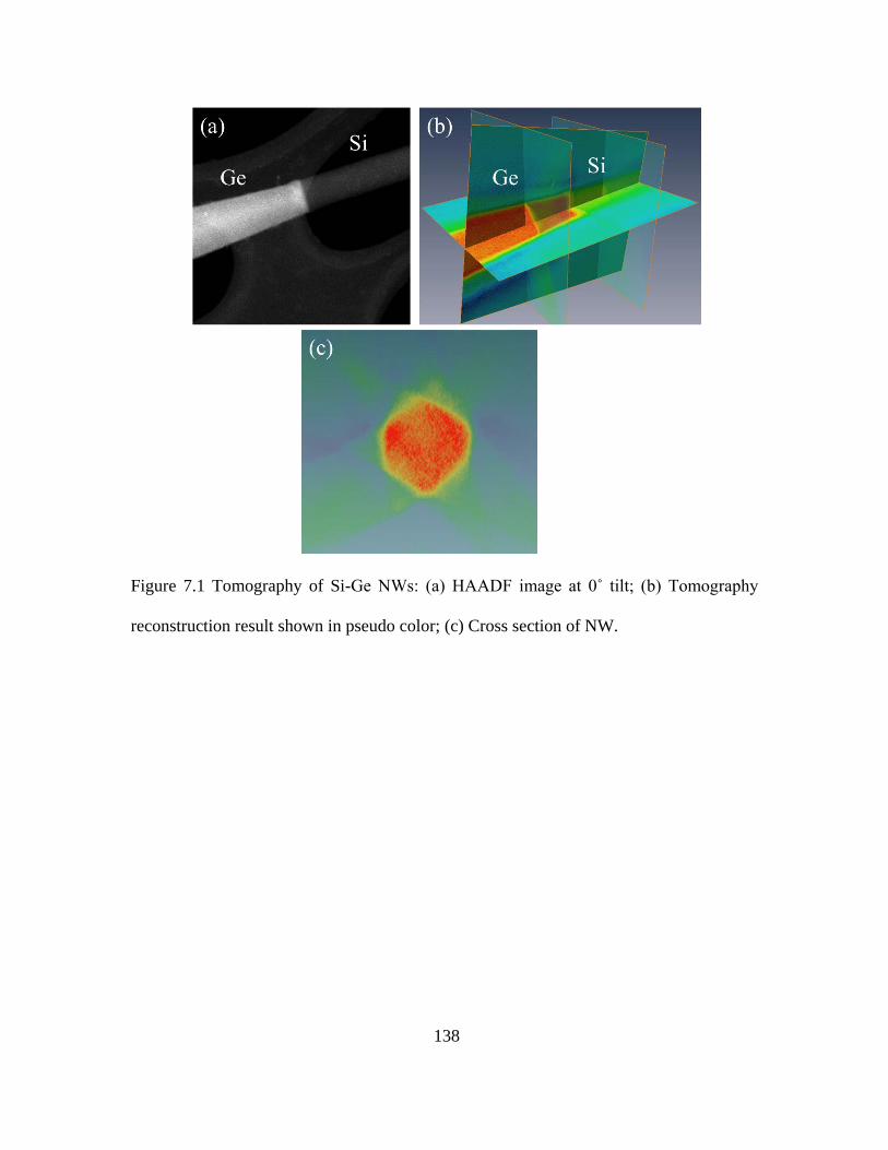
Figure 7.1 Tomography of Si-Ge NWs: (a) HAADF image at 0˚ tilt; (b) Tomography
reconstruction result shown in pseudo color; (c) Cross section of NW.
138

References
[1] Z. Gan, D. E. Perea, J. Yoo, S. Tom Picraux, D. J. Smith, and M. R. McCartney, Applied Physics Letters 103 153108 (2013).
[2] Z. Gan, D. Perea, J. Yoo, Y. He, R. Colby, B. Barker, M. Gu, S. Mao, C. Wang, S. Tom Picraux, D. J. Smith, and M. R. McCartney, submitted (2015).
[3] J. Frank, Electron tomography : three-dimensional imaging with the transmission electron microscope. Plenum Press, New York, (1992).
[4] A. C. Twitchett-Harrison, T. J. Yates, R. E. Dunin-Borkowski, and P. A. Midgley, Ultramicroscopy 108 1401 (2008).
139
LIST OF REFERENCES
A. C. Twitchett-Harrison, T. J. Yates, R. E. Dunin-Borkowski, and P. A. Midgley, Ultramicroscopy 108 1401 (2008).
A. C. Jones, M. L. Hitchman, and Knovel (Firm), Chemical vapour deposition precursors, processes and applications. Royal Society of Chemistry, Cambridge, UK, (2009).
A. Lubk, D. Wolf, and H. Lichte, Ultramicroscopy 110 438 (2010).
A. S. Arico, P. Bruce, B. Scrosati, J.-M. Tarascon, and W. Van Schalkwijk, Nature materials 4 366 (2005).
A. Sekar, S. H. Kim, A. Umar, and Y. B. Hahn, Journal of Crystal Growth 277 471 (2005).
A. T. Heitsch, D. D. Fanfair, H.-Y. Tuan, and B. A. Korgel, J Am Chem Soc 130 5436 (2008).
A. Tonomura, Reviews of Modern Physics 59 639 (1987).
A. Umar and Y. B. Hahn, Nanotechnology 17 2174 (2006).
A. Umar, S. H. Kim, Y. S. Lee, K. S. Nahm, and Y. B. Hahn, Journal of Crystal Growth 282 131 (2005).
A. Umar, S. Lee, Y. S. Lee, K. S. Nahm, and Y. B. Hahn, Journal of Crystal Growth 277 479 (2005).
A. V. Crewe and J. Wall, Journal of Molecular Biology 48 375 (1970).
B. G. Yacobi, Semiconductor materials : an introduction to basic principles. Kluwer Academic/Plenum Publishers, New York, (2003).
B. Key, R. Bhattacharyya, M. Morcrette, V. Seznéc, J.-M. Tarascon, and C. P. Grey, J Am Chem Soc 131 9239 (2009).
B. P. Zhang, N. T. Binh, K. Wakatsuki, Y. Segawa, Y. Yamada, N. Usami, M. Kawasaki, and H. Koinuma, Applied Physics Letters 84 4098 (2004).
B. Pal and M. Sharon, Mater Chem Phys 76 82 (2002).
C. C. Ahn, Transmission electron energy loss spectrometry in materials science and the EELS atlas, 2nd ed. Wiley, Weinheim, Germany, (2004).
C. Fuller and J. Severiens, Physical Review 96 21 (1954).
140
C. J. Lee, T. J. Lee, S. C. Lyu, Y. Zhang, H. Ruh, and H. J. Lee, Applied Physics Letters 81 3648 (2002).
C. K. Chan, H. Peng, G. Liu, K. McIlwrath, X. F. Zhang, R. A. Huggins, and Y. Cui, Nat Nano 3 31 (2008).
C. Y. Wen, M. C. Reuter, J. Bruley, J. Tersoff, S. Kodambaka, E. A. Stach, and F. M. Ross, Science 326 1247 (2009).
D. A. Neamen, Semiconductor physics and devices : basic principles, 2nd ed. Irwin, Chicago, (1997).
D. A. Neamen, Semiconductor physics and devices : basic principles, 3rd ed. McGraw-Hill Higher Education, London, (2003).
D. B. Williams and C. B. Carter, Transmission electron microscopy : a textbook for materials science, 2nd ed. Springer, New York, (2009).
D. C. Ghiglia and M. D. Pritt, Two-dimensional phase unwrapping : theory, algorithms, and software. Wiley, New York, (1998).
D. Cooper, C. Ailliot, J.-P. Barnes, J.-M. Hartmann, P. Salles, G. Benassayag, and R. E. Dunin-Borkowski, Ultramicroscopy 110 383 (2010).
D. E. Perea, E. R. Hemesath, E. J. Schwalbach, J. L. Lensch-Falk, P. W. Voorhees, and L. J. Lauhon, Nature nanotechnology 4 315 (2009).
D. E. Perea, E. Wijaya, J. L. Lensch-Falk, E. R. Hemesath, and L. J. Lauhon, Journal of Solid State Chemistry 181 1642 (2008).
D. E. Perea, N. Li, R. M. Dickerson, A. Misra, and S. T. Picraux, Nano letters 11 3117 (2011).
D. Gabor, Proceedings of the Royal Society of London. Series A. Mathematical and Physical Sciences 197 454 (1949).
D. Larcher, S. Beattie, M. Morcrette, K. Edstrom, J.-C. Jumas, and J.-M. Tarascon, Journal of Materials Chemistry 17 3759 (2007).
E. Koren, N. Berkovitch, O. Azriel, A. Boag, Y. Rosenwaks, E. R. Hemesath, and L. J. Lauhon, Applied Physics Letters 99 223511 (2011).
E. Müller, P. Kruse, D. Gerthsen, M. Schowalter, A. Rosenauer, D. Lamoen, R. Kling, and A. Waag, Applied Physics Letters 86 154108 (2005).
E. N. Leith and J. Upatnieks, J. Opt. Soc. Am. 52 1123 (1962).
F. A. Trumbore, Bell System Technical Journal 39 205 (1960). 141
F. M. Ross and W. M. Stobbs, Philosophical Magazine A 63 37 (1991).
F. Qian, Y. Li, S. Gradecak, D. L. Wang, C. J. Barrelet, and C. M. Lieber, Nano letters 4 1975 (2004).
G. E. Moore, Proceedings of the IEEE 86 82 (1998).
G. Mandel, Physical Review 134 A1073 (1964).
G. Möllenstedt and H. Wahl, Naturwissenschaften 55 340 (1968).
G. Radi, Acta Crystallographica Section A 26 41 (1970).
G. Sberveglieri, S. Groppelli, P. Nelli, A. Tintinelli, and G. Giunta, Sensors and Actuators B: Chemical 25 588 (1995).
G.-C. Yi, Semiconductor Nanostructures for Optoelectronic Devices Processing, Characterization and Applications, Springer, Heidelberg, (2012).
H. Bethe, Ann. Phys. 87 55 (1928).
H. Kai, C. Jeong-Hyun, J. Yeonwoong, S. T. Picraux, and C. John, Nanotechnology 24 115703 (2013).
H. Lichte, P. Formanek, A. Lenk, M. Linck, C. Matzeck, M. Lehmann, and P. Simon, Annual Review of Materials Research 37 539 (2007).
H. Wu and Y. Cui, Nano Today 7 414 (2012).
I. Kimukin, M. S. Islam, and R. S. Williams, Nanotechnology 17 S240 (2006).
I. W. Tao, M. Jurkovic, and W. I. Wang, Applied Physics Letters 64 1848 (1994).
International Technology Roadmap for Semiconductors 2013, available online at http://www.itrs.net.
J. C. H. Spence and J. M. Zuo, Electron microdiffraction. Plenum Press, New York, (1992).
J. E. Allen, E. R. Hemesath, D. E. Perea, J. L. Lensch-Falk, Z. Y. Li, F. Yin, M. H. Gass, P. Wang, A. L. Bleloch, R. E. Palmer, and L. J. Lauhon, Nature nanotechnology 3 168 (2008).
J. Frank, Electron tomography : three-dimensional imaging with the transmission electron microscope. Plenum Press, New York, (1992).
J. Goldberger, A. I. Hochbaum, R. Fan, and P. Yang, Nano letters 6 973 (2006).
142
J. Graetz, C. C. Ahn, R. Yazami, and B. Fultz, Journal of The Electrochemical Society 151 A698 (2004).
J. Ibers, Acta Crystallographica 11 178 (1958).
J. J. Lee, Y. B. Kim, and Y. S. Yoon, Applied Surface Science 244 365 (2005).
J. Li, M. R. McCartney, and D. J. Smith, Ultramicroscopy 94 149 (2003).
J. Li, M. R. McCartney, R. E. Dunin-Borkowski, and D. J. Smith, Acta Crystallographica Section A 55 652 (1999).
J. M. Cowley, Ultramicroscopy 41 335 (1992).
J. Q. Hu, Y. Bando, J. H. Zhan, Y. B. Li, and T. Sekiguchi, Applied Physics Letters 83 4414 (2003).
J. Spence, Acta Crystallographica Section A 49 231 (1993).
J. W. Dailey, J. Taraci, T. Clement, D. J. Smith, J. Drucker, and S. T. Picraux, J Appl Phys 96 7556 (2004).
J. Xiang, W. Lu, Y. Hu, Y. Wu, H. Yan, and C. M. Lieber, Nature 441 489 (2006).
J. Y. Tsao, Materials fundamentals of molecular beam epitaxy. Academic Press, Boston, (1993).
J.-J. Wu, S.-C. Liu, C.-T. Wu, K.-H. Chen, and L.-C. Chen, Applied Physics Letters 81 1312 (2002).
K. B. Wolfstirn, Journal of Physics and Chemistry of Solids 16 279 (1960).
K. Sato, M. Hanafusa, A. Noda, A. Arakawa, M. Uchida, T. Asahi, and O. Oda, Journal of Crystal Growth 214–215 1080 (2000).
L. Baggetto and P. H. L. Notten, Journal of The Electrochemical Society 156 A169 (2009).
L. Chen, W. Y. Fung, and W. Lu, Nano letters 13 5521 (2013).
L. J. Lauhon, M. S. Gudiksen, C. L. Wang, and C. M. Lieber, Nature 420 57 (2002).
L. Ji, Z. Lin, M. Alcoutlabi, and X. Zhang, Energy & Environmental Science 4 2682 (2011).
L. Li, D. J. Smith, E. Dailey, P. Madras, J. Drucker, and M. R. McCartney, Nano letters 11 493 (2011).
143
L. Li, Z. Gan, M. R. McCartney, H. Liang, H. Yu, W. J. Yin, Y. Yan, Y. Gao, J. Wang, and D. J. Smith, Adv Mater 26 1052 (2014).
L. Reimer, Transmission electron microscopy : physics of image formation and microanalysis, 4th ed. Springer, New York, (1997).
L. Y. Beaulieu, K. W. Eberman, R. L. Turner, L. J. Krause, and J. R. Dahn, Electrochemical and Solid-State Letters 4 A137 (2001).
MultiPrepTM operating manual of Allied High Tech Products, Inc.
M. A. Herman and H. Sitter, Molecular beam epitaxy : fundamentals and current status, 2nd, rev. and updated ed. Springer, New York, (1996).
M. Armand and J. M. Tarascon, Nature 451 652 (2008).
M. Faraday, Experimental researches in electricity. R. and J.E. Taylor, London, (1839).
M. Gajdardziska-Josifovska and A. H. Carim, Chapter 12, Introduction to electron holography, Kluwer Academic/Plenum Publishers, New York, (1999).
M. Gajdardziska-Josifovska, M. R. McCartney, W. J. de Ruijter, D. J. Smith, J. K. Weiss, and J. M. Zuo, Ultramicroscopy 50 285 (1993).
M. Gu, H. Yang, D. E. Perea, J. G. Zhang, S. Zhang, and C. M. Wang, Nano letters 14 4622 (2014).
M. H. Huang, S. Mao, H. Feick, H. Yan, Y. Wu, H. Kind, E. Weber, R. Russo, and P. Yang, Science 292 1897 (2001).
M. I. den Hertog, H. Schmid, D. Cooper, J. L. Rouviere, M. T. Bjork, H. Riel, P. Rivallin, S. Karg, and W. Riess, Nano letters 9 3837 (2009).
M. J. Hytch, E. Snoeck, and R. Kilaas, Ultramicroscopy 74 131 (1998).
M. Lehmann and H. Lichte, Microscopy and Microanalysis 8 447 (2004).
M. Lehmann, Ultramicroscopy 100 9 (2004).
M. N. Obrovac and L. Christensen, Electrochemical and Solid-State Letters 7 A93 (2004).
M. N. Obrovac and L. J. Krause, Journal of The Electrochemical Society 154 A103 (2007).
M. R. McCartney and D. J. Smith, Annual Review of Materials Research 37 729 (2007).
M. R. McCartney and M. Gajdardziska-Josifovska, Ultramicroscopy 53 283 (1994). 144
M. R. McCartney, N. Agarwal, S. Chung, D. A. Cullen, M.-G. Han, K. He, L. Li, H. Wang, L. Zhou, and D. J. Smith, Ultramicroscopy 110 375 (2010).
M. S. Gudiksen, L. J. Lauhon, J. Wang, D. C. Smith, and C. M. Lieber, Nature 415 617 (2002).
M. Schowalter, D. Lamoen, A. Rosenauer, P. Kruse, and D. Gerthsen, Applied Physics Letters 85 4938 (2004).
M. Y. Kim, J. M. Zuo, and J. C. H. Spence, physica status solidi (a) 166 445 (1998).
M.-S. Kim and Y.-M. Sung, Chem Mater 25 4156 (2013).
N. Li, T. Y. Tan, and U. Gösele, Applied Physics A 90 591 (2008).
N. Ohashi, K. Kataoka, T. Ohgaki, T. Miyagi, H. Haneda, and K. Morinaga, Applied Physics Letters 83 4857 (2003).
N. Sclar, Electron Devices, IEEE Transactions on 24 709 (1977).
O. Hayden, A. B. Greytak, and D. C. Bell, Advanced Materials 17 701 (2005).
O. Hiroshi, I. Gheyas Syed, N. Hitoshi, N. Mitsuhiro, and Y. Akira, Japanese Journal of Applied Physics 33 L980 (1994).
P. A. Doyle and P. S. Turner, Acta Crystallographica Section A 24 390 (1968).
P. A. Tipler, Modern physics. Worth Publishers, New York, (1978).
P. Becker and P. Coppens, Acta Crystallographica Section A 46 254 (1990).
P. G. Bruce, B. Scrosati, and J.-M. Tarascon, Angewandte Chemie International Edition 47 2930 (2008).
P. Hartel, H. Rose, and C. Dinges, Ultramicroscopy 63 93 (1996).
P. M. Voyles, D. A. Muller, J. L. Grazul, P. H. Citrin, and H. J. Gossmann, Nature 416 826 (2002).
R. Agarwal, Small 4 1872 (2008).
R. F. Egerton, Electron energy-loss spectroscopy in the electron microscope, 2nd ed. Plenum Press, New York, (1996).
R. S. Wagner and W. C. Ellis, Applied Physics Letters 4 89 (1964).
S. A. Dayeh, J. Wang, N. Li, J. Y. Huang, A. V. Gin, and S. T. Picraux, Nano letters 11 4200 (2011). 145
S. A. Dayeh, N. H. Mack, J. Y. Huang, and S. T. Picraux, Applied Physics Letters 99 023102 (2011).
S. Baosheng, Y. Akira, and K. Makoto, Japanese Journal of Applied Physics 37 L206 (1998).
S. Dimitrijev, Understanding semiconductor devices. Oxford University Press, New York, (2000).
S. Ingole, P. Manandhar, S. B. Chikkannanavar, E. A. Akhadov, and S. T. Picraux, Electron Devices, IEEE Transactions on 55 2931 (2008).
S. J. Pennycook, P. D. Nellist, Scanning Transmission Electron Microscopy Imaging and Analysis. Springer, New York, NY, (2011).
S. M. Sze, Physics of semiconductor devices, 2nd ed. Wiley, New York, (1981).
S. M. Sze, Physics of semiconductor devices. Wiley-Interscience, New York, (1969).
S. M. Sze, Semiconductor devices, physics and technology, 2nd ed. Wiley, New York, (2002).
S. Miyake, Proc. Phys. Math. Soc. Japan 22 666 (1940).
T. E. Clark, P. Nimmatoori, K.-K. Lew, L. Pan, J. M. Redwing, and E. C. Dickey, Nano letters 8 1246 (2008).
T. Hoshikawa, X. Huang, K. Hoshikawa, and S. Uda, Japanese Journal of Applied Physics 47 8691 (2008).
T. Tanaka, K. Hayashida, K. Saito, M. Nishio, Q. Guo, and H. Ogawa, physica status solidi (b) 243 959 (2006).
T. Tanaka, N. Murata, K. Saito, M. Nishio, Q. Guo, and H. Ogawa, physica status solidi (b) 244 1685 (2007).
T. Tanaka, Q. Guo, M. Nishio, and H. Ogawa, Journal of Physics: Conference Series 61 1162 (2007).
T. Teiji, M. Toyosaka, and T. Kiyoshi, Japanese Journal of Applied Physics 11 1024 (1972).
U. K. Mishra, J. Singh, Semiconductor device physics and design. Springer, Dordrecht, The Netherlands, (2008).
U. Özgür, Y. I. Alivov, C. Liu, A. Teke, M. A. Reshchikov, S. Doğan, V. Avrutin, S. J. Cho, and H. Morkoç, Journal of Applied Physics 98 041301 (2005).
146
V. Schmidt, H. Riel, S. Senz, S. Karg, W. Riess, and U. Gosele, Small 2 85 (2006).
V. Schmidt, J. V. Wittemann, S. Senz, and U. Gösele, Advanced Materials 21 2681 (2009).
W. D. Callister, T. L. Larsen, C. F. Varotto, and D. A. Stevenson, Journal of Physics and Chemistry of Solids 33 1433 (1972).
W. Lu, J. Xiang, B. P. Timko, Y. Wu, and C. M. Lieber, Proc. Nat. Acad. Sci. 102 10046 (2005).
W. Lu, P. Xie, and C. M. Lieber, IEEE Transactions on Electron Devices 55 2859 (2008).
X. H. Liu and J. Y. Huang, Energy & Environmental Science 4 3844 (2011).
X. H. Liu, H. Zheng, L. Zhong, S. Huang, K. Karki, L. Q. Zhang, Y. Liu, A. Kushima, W. T. Liang, J. W. Wang, J. H. Cho, E. Epstein, S. A. Dayeh, S. T. Picraux, T. Zhu, J. Li, J. P. Sullivan, J. Cumings, C. Wang, S. X. Mao, Z. Z. Ye, S. Zhang, and J. Y. Huang, Nano letters 11 3312 (2011).
X. H. Liu, J. W. Wang, S. Huang, F. Fan, X. Huang, Y. Liu, S. Krylyuk, J. Yoo, S. A. Dayeh, A. V. Davydov, S. X. Mao, S. T. Picraux, S. Zhang, J. Li, T. Zhu, and J. Y. Huang, Nature nanotechnology 7 749 (2012).
X. H. Liu, L. Q. Zhang, L. Zhong, Y. Liu, H. Zheng, J. W. Wang, J. H. Cho, S. A. Dayeh, S. T. Picraux, J. P. Sullivan, S. X. Mao, Z. Z. Ye, and J. Y. Huang, Nano letters 11 2251 (2011).
X. H. Liu, S. Huang, S. T. Picraux, J. Li, T. Zhu, and J. Y. Huang, Nano letters 11 3991 (2011).
X. H. Liu, Y. Liu, A. Kushima, S. Zhang, T. Zhu, J. Li, and J. Y. Huang, Advanced Energy Materials 2 722 (2012).
X. Y. Kong, Y. Ding, R. Yang, and Z. L. Wang, Science 303 1348 (2004).
Y. C. Kong, D. P. Yu, B. Zhang, W. Fang, and S. Q. Feng, Applied Physics Letters 78 407 (2001).
Y. Cui, Q. Wei, H. Park, and C. M. Lieber, Science 293 1289 (2001).
Y. Hu, H. O. Churchill, D. J. Reilly, J. Xiang, C. M. Lieber, and C. M. Marcus, Nature nanotechnology 2 622 (2007).
Y. Li, G. W. Meng, L. D. Zhang, and F. Phillipp, Applied Physics Letters 76 2011 (2000).
147
Y. Liu, S. Zhang, and T. Zhu, ChemElectroChem 1 706 (2014).
Y. Liu, X. H. Liu, B. M. Nguyen, J. Yoo, J. P. Sullivan, S. T. Picraux, J. Y. Huang, and S. A. Dayeh, Nano letters 13 4876 (2013).
Y. Wu, Y. Cui, L. Huynh, C. J. Barrelet, D. C. Bell, and C. M. Lieber, Nano letters 4 433 (2004).
Y.-C. Chou, C.-Y. Wen, M. C. Reuter, D. Su, E. A. Stach, and F. M. Ross, ACS Nano 6 6407 (2012).
Y.-M. Chiang, Science 330 1485 (2010).
Z. Gan, D. E. Perea, J. Yoo, S. Tom Picraux, D. J. Smith, and M. R. McCartney, Applied Physics Letters 103 153108 (2013).
Z. Gan, D. Perea, J. Yoo, Y. He, R. Colby, B. Barker, M. Gu, S. Mao, C. Wang, S. Tom Picraux, D. Smith, and M. McCartney, Unpublished (2015).
Z. L. Wang, Journal of Physics: Condensed Matter 16 R829 (2004).
Z. W. Pan, Z. R. Dai, and Z. L. Wang, Science 291 1947 (2001).
148