Embed Size (px)
Citation preview
TITLE PAGE OPTICAL AND MECHANICAL CHARACTERIZATION AND ANALYSIS OF
NANOSCALE SYSTEMS
by
Daniel N. Lamont
B.S. in Chemistry, University of Pittsburgh, 2004
Submitted to the Graduate Faculty of the
Kenneth P. Dietrich School of Arts and Sciences in partial fulfillment
of the requirements for the degree of
Doctor of Philosophy
University of Pittsburgh
2016

COMMITTEE PAGEUNIVERSITY OF PITTSBURGH
DIETRICH SCHOOL OF ARTS AND SCIENCES
This dissertation was presented
by
Daniel N. Lamont
It was defended on
August 5, 2016
and approved by
Geoffrey R. Hutchison, PhD, Assistant Professor
Hrvoje Petek, PhD, Professor
Gilbert C. Walker, PhD, Professor
Dissertation Advisor: David H. Waldeck, PhD, Professor
ii

iii
Copyright © by Daniel N. Lamont
2016
OPTICAL AND MECHANICAL CHARACTERIZATION AND ANALYSIS OFNANOSCALE SYSTEMS
ABSTRACTDaniel N. Lamont, Ph.D.
University of Pittsburgh, 2016
This thesis discusses research focused on the analysis and characterization of nanoscale systems.
These studies are organized into three sections based on the research topic and methodology:
Part I describes research using scanning probe microscopy, Part II describes research using
photonic crystals and Part III describes research using spectroscopy. A brief description of the
studies contained in each part follows. Part I discusses our work using scanning probe
microscopy. In Chapter 3, we present our work using apertureless scanning near-field optical
microscopy to study the optical properties of an isolated subwavelength slit in a gold film, while
in chapter 4 atomic force microscopy and a three point bending model are used to explore the
mechanical properties of individual multiwall boron nitride nanotubes. Part II includes our
studies of photonic crystals. In Chapter 6 we discuss the fabrication and characterization of a
photonic crystal material that utilizes electrostatic colloidal crystal array self assembly to form a
highly ordered, non closed packed template; and in Chapter 7 we discuss the fabrication and
characterization of a novel, simple and efficient approach to rapidly fabricate large-area 2D
particle arrays on water surfaces. Finally, in Part III we present our spectroscopic studies. In
Chapter 9 we use fluorescence quenching and fluorescence lifetime measurements to study
electron transfer in aggregates of cadmium selenide and cadmium telluride nanoparticles
assemblies. Chapter 10 features our work using the electronic structure of zinc sulfide
iv

semiconductor nanoparticles to sensitize the luminescence of Tb3+ and Eu3+ lanthanide cations,
and Chapter 11 presents our recent work studying photo-induced electron transfer between donor
and acceptor moieties attached to a cleft-forming bridge.
v

TABLE OF CONTENTS
PREFACE.....................................................................................................................................xxi
1.0 INTRODUCTION.....................................................................................................................1
2.0 SCANNING PROBE MICROSCOPY INTRODUCTION.......................................................4
2.1 PAST, PRESENT, AND FUTURE OF NANOSCOPY........................................................4
2.2 OPTICAL MICROSCOPY..................................................................................................5
2.3 ELECTRON MICROSCOPY..............................................................................................5
2.4 SCANNING PROBE MICROSCOPY................................................................................6
2.5 MOTIVATION FOR MICROSCOPY DEVELOPMENT...................................................7
2.6 SUPER-RESOLUTION FRAMEWORK............................................................................8
2.6.1 Limitations of Optics....................................................................................................8
2.6.2 Near-field Optics........................................................................................................10
2.7 SPECIFIC SPM TECHNIQUES........................................................................................11
2.8 FORCE-DISTANCE CURVES..........................................................................................11
2.9 APERTURELESS NEAR-FIELD OPTICAL MICROSCOPY.........................................13
2.10 FUTURE OF SCANNING PROBE MICROSCOPY (SPM)..........................................15
2.11 BIBLIOGRAPHY............................................................................................................16
3.0 OBSERVATION AND ANALYSIS OF LOCALIZED OPTICAL SCATTERING WITH
NON-PASSIVE PROBES..............................................................................................................17
vi

3.1 INTRODUCTION..............................................................................................................17
3.2 EXPERIMENTAL DETAILS............................................................................................22
3.2.1 Deposition of Metal Film...........................................................................................22
3.2.2 Fabrication of Nanoslits.............................................................................................22
3.2.3 Near-field Microscopy................................................................................................23
3.3 RESULTS AND DISCUSSION.........................................................................................28
3.3.1 Lateral ANSOM Images of a Single Metallic Nanoslit..............................................28
3.3.2 Model: Superposition of Background and Probe Scattered Fields.............................31
3.4 SUMMARY AND CONCLUSIONS.................................................................................40
3.5 BIBLIOGRAPHY..............................................................................................................42
4.0 DIAMETER-DEPENDENT BENDING MODULUS OF INDIVIDUAL MULTIWALL
BORON NITRIDE NANOTUBES...............................................................................................49
4.1 INTRODUCTION..............................................................................................................49
4.2 EXPERIMENTAL METHODS.........................................................................................52
4.3 RESULTS AND DISCUSSION.........................................................................................54
4.3.1 Characterization of MWBNNTs.................................................................................54
4.3.2 AFM Three-Point Bending.........................................................................................58
4.3.3 Elastic Properties........................................................................................................67
4.4 CONCLUSIONS................................................................................................................76
4.5 BIBLIOGRAPHY..............................................................................................................78
5.0 PHOTONIC CRYSTALS INTRODUCTION.........................................................................82
5.1 THE PHOTONIC BAND GAP..........................................................................................85
5.2 DEFECTS AND DISORDER IN PHOTONIC CRYSTALS.............................................89
vii

5.3 BIBLIOGRAPHY..............................................................................................................91
6.0 CHARGE STABILIZED CRYSTALLINE COLLOIDAL ARRAYS AS TEMPLATES FOR
FABRICATION OF NON-CLOSE-PACKED INVERTED PHOTONIC CRYSTALS................92
6.1 INTRODUCTION..............................................................................................................92
6.2 EXPERIMENTAL METHODS.........................................................................................97
6.2.1 Materials.....................................................................................................................97
6.2.2 Preparation of PCCA..................................................................................................99
6.2.3 Infiltration of Sol-gel Precursor................................................................................100
6.2.4 Solvent Removal......................................................................................................100
6.2.5 Polymer Removal.....................................................................................................100
6.2.6 Physical Measurements............................................................................................101
6.3 RESULTS AND DISCUSSION.......................................................................................103
6.3.1 Photonic Crystal Structure........................................................................................103
6.3.2 Wall Spacing and Periodicity of siPCCA, Surface Morphology..............................115
6.3.3 Ordering....................................................................................................................118
6.4 CONCLUSIONS..............................................................................................................131
6.5 BIBLIOGRAPHY............................................................................................................133
7.0 FABRICATION OF LARGE-AREA TWO-DIMENSIONAL COLLOIDAL CRYSTALS. 139
7.1 INTRODUCTION............................................................................................................139
7.2 RESULTS AND DISCUSSION.......................................................................................143
7.3 EXPERIMENTAL SECTION..........................................................................................151
7.4 BIBLIOGRAPHY............................................................................................................152
8.0 SPECTROSCOPY INTRODUCTION..................................................................................155
viii
8.1 INTRODUCTION............................................................................................................155
8.2 STEADY-STATE AND TIME-RESOLVED FLUORESCENCE....................................156
8.3 FLUORESCENCE LIFETIMES AND QUANTUM YIELDS.......................................157
8.4 FLUORESCENCE QUENCHING..................................................................................158
8.5 RESONANCE ENERGY TRANSFER...........................................................................159
8.6 TIME-RESOLVED LIFETIME MEASUREMENTS.....................................................160
8.6.1 Intensity Decay Laws...............................................................................................161
8.6.2 Multi-Exponential Decay.........................................................................................162
8.6.3 Lifetime Distributions..............................................................................................162
8.7 APPLICATION OF FLUORESCENCE..........................................................................163
8.8 BIBLIOGRAPHY............................................................................................................165
9.0 ELECTRON TRANSFER AND FLUORESCENCE QUENCHING OF NANOPARTICLE
ASSEMBLIES.............................................................................................................................166
9.1 INTRODUCTION............................................................................................................166
9.2 EXPERIMENTAL DETAILS..........................................................................................169
9.2.1 Materials and Methods.............................................................................................169
9.2.2 CdSe NP Synthesis and Ligand Exchange...............................................................170
9.2.3 CdTe NP Synthesis...................................................................................................171
9.2.4 Steady-State Spectroscopy.......................................................................................173
9.2.5 Time-Dependent Fluorescence Spectroscopy...........................................................173
9.2.6 Dynamic Light Scattering (DLS) and ζ Potential Measurements............................174
9.3 RESULTS AND DISCUSSION.......................................................................................174
9.3.1 Formation of Aggregates Through Electrostatic Interaction....................................174
ix
9.3.2 Aggregation-Induced Self-Quenching Due to Interparticle Interaction...................179
9.3.3 Charge Transfer Process from CdTe to CdSe NPs...................................................182
9.3.4 Interparticle Distance Dependence...........................................................................182
9.3.5 Surface Charge Dependence.....................................................................................189
9.3.6 Kinetic Measurements..............................................................................................191
9.4 SUMMARY AND CONCLUSIONS...............................................................................196
9.5 BIBLIOGRAPHY............................................................................................................200
10.0 LANTHANIDE SENSITIZATION IN II−VI SEMICONDUCTOR MATERIALS: A CASE
STUDY WITH TERBIUM(III) AND EUROPIUM(III) IN ZINC SULFIDE NANOPARTICLES
......................................................................................................................................................205
10.1 INTRODUCTION..........................................................................................................205
10.2 MATERIALS AND METHODS....................................................................................210
10.2.1 Chemicals...............................................................................................................210
10.2.2 Nanoparticle Synthesis...........................................................................................210
10.2.3 Steady-State Optical Measurements.......................................................................211
10.2.4 Quantum Yields......................................................................................................211
10.2.5 Time-Gated Measurements.....................................................................................213
10.2.6 Time-Resolved Measurements...............................................................................213
10.3 RESULTS AND DISCUSSION.....................................................................................214
10.3.1 HRTEM Imaging....................................................................................................214
10.3.2 Absorption Spectra.................................................................................................217
10.3.3 ZnS/Tb Spectra.......................................................................................................219
10.3.4 ZnS/Eu Spectra.......................................................................................................223
x

10.3.5 ZnS/Gd Spectra......................................................................................................225
10.3.6 ZnS Spectra............................................................................................................225
10.3.7 Time-Gated Excitation and Emission Spectra........................................................226
10.3.8 ZnS Luminescence Lifetime Measurements..........................................................229
10.3.9 ZnS/Tb Samples.....................................................................................................229
10.3.10 ZnS/Eu Samples...................................................................................................230
10.3.11 ZnS/Gd Samples...................................................................................................231
10.3.12 ZnS Samples.........................................................................................................231
10.3.13 Lanthanide Ion Luminescence Lifetime Measurements.......................................232
10.3.14 A Mechanism for Sensitization of Lanthanide Luminescence.............................234
10.4 CONCLUSION..............................................................................................................246
10.5 BIBLIOGRAPHY..........................................................................................................248
11.0 THROUGH SOLVENT TUNNELING IN DONOR-BRIDGE-ACCEPTOR MOLECULES
CONTAINING A MOLECULAR CLEFT..................................................................................253
11.1 INTRODUCTION..........................................................................................................253
11.2 EXPERIMENTAL..........................................................................................................258
11.2.1 Synthesis.................................................................................................................258
11.2.2 Photophysics..........................................................................................................259
11.3 RESULTS.......................................................................................................................261
11.3.1 Photophysical Model..............................................................................................261
11.3.2 Kinetic Analysis......................................................................................................269
11.3.3 Electron Transfer Rate Analysis.............................................................................277
11.4 DISCUSSION................................................................................................................282
xi

11.5 CONCLUSION..............................................................................................................287
11.6 BIBLIOGRAPHY..........................................................................................................288
12.0 CONCLUSIONS..................................................................................................................292
xii

LIST OF TABLES
Table 1: Polymer heat treatment..................................................................................................109
Table 2: First excitonic Peak and PL Peak of NPs.......................................................................172
Table 3: Time-resolved PL decay parameters..............................................................................195
Table 4: Reaction free energy for the DBA oligomers 1 and 2 in different solvents, in eV........276
Table 5: The activation Gibbs energy (ΔG‡), solvent reorganization energy (λs), and electronic
coupling (|V|) of 1 and 2 in different solvents at 298 K...............................................................279
Table 6: Parameters for the CS state dipole moment and solute-solvent complex geometries. . .281
xiii

LIST OF FIGURES
Figure 3.1: Instrument schematic..................................................................................................25
Figure 3.2: ANSOM probe drawings............................................................................................27
Figure 3.3: Lateral ANSOM imaging with extended probe..........................................................30
Figure 3.4: Simulated phase calculation.......................................................................................35
Figure 3.5: ANSOM imaging with traditional probe....................................................................37
Figure 3.6: Scattering surfaces......................................................................................................38
Figure 4.1: SEM image of MWBNNTs........................................................................................55
Figure 4.2: FTIR spectrum of MWBNNTs...................................................................................57
Figure 4.3: Beam schematics........................................................................................................60
Figure 4.4: SEM image of MWBNNTs........................................................................................63
Figure 4.5: Force curve.................................................................................................................64
Figure 4.6: Tube effective stiffness (keff) vs position..................................................................66
Figure 4.7: Bending modulus vs tube outer diameter...................................................................69
Figure 4.8: Determination of the Young’s modulus and shear modulus.......................................74
Figure 5.1: Schematic of 1D photonic crystal..............................................................................84
Figure 6.1: Synthetic scheme for fabricating an inverted photonic crystal..................................98
Figure 6.2: Melting polystyrene colloidal particles....................................................................102
Figure 6.3: Heat treatment of the siPCCA..................................................................................105
xiv

Figure 6.4: Diffraction spectra of siPCCA.................................................................................108
Figure 6.5: Void volume of siPCCA...........................................................................................111
Figure 6.6: 450 °C heat treated siPCCA.....................................................................................116
Figure 6.7: siPCCA plateau regions............................................................................................117
Figure 6.8: siPCCA 100 planes...................................................................................................121
Figure 6.9: siPCCA 111 planes...................................................................................................122
Figure 6.10: Pair correlation function.........................................................................................123
Figure 6.11: Dependence of UDLVO(r) upon interparticle distance..........................................127
Figure 6.12: Model for response of one dimensional array of N particles to a single defect
particle..........................................................................................................................................129
Figure 7.1: Fabrication of a 2D PS particle array by the needle tip flow technique....................142
Figure 7.2: Pair correlation function...........................................................................................146
Figure 7.3: Fabrication with substrate transfer...........................................................................147
Figure 7.4: Fabrication with two particle diameters...................................................................148
Figure 7.5: pH sensing................................................................................................................150
Figure 9.1: Abbreviations, definitions, and structures................................................................170
Figure 9.2: Absorption and PL spectra of MPA-capped CdTe and TMA-capped CdSe NPs.....176
Figure 9.3: ζ potential measurements of assemblies of CdSe/CdTe...........................................178
Figure 9.4: PL spectra and relative PL intensity of MPA-CdTe assemblies with increasing
concentration of TMA-CdSe........................................................................................................181
Figure 9.5: PL spectra of MPA-CdTe NPs in water with increasing DEA-CdSe concentration 183
Figure 9.6: PL spectra of MPA-CdTe NP with the addition of quencher NPs............................185
Figure 9.7: Drawing of type II and type I staggered band gap alignment..................................188
xv
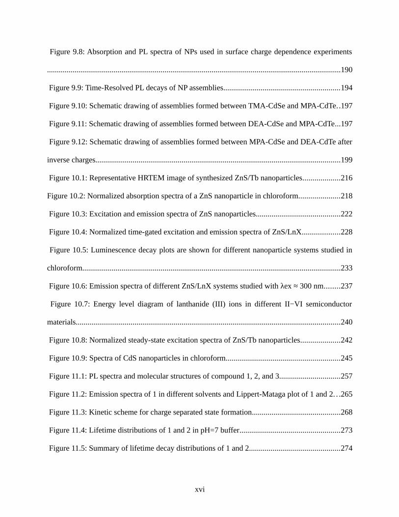
Figure 9.8: Absorption and PL spectra of NPs used in surface charge dependence experiments
......................................................................................................................................................190
Figure 9.9: Time-Resolved PL decays of NP assemblies...........................................................194
Figure 9.10: Schematic drawing of assemblies formed between TMA-CdSe and MPA-CdTe..197
Figure 9.11: Schematic drawing of assemblies formed between DEA-CdSe and MPA-CdTe...197
Figure 9.12: Schematic drawing of assemblies formed between MPA-CdSe and DEA-CdTe after
inverse charges.............................................................................................................................199
Figure 10.1: Representative HRTEM image of synthesized ZnS/Tb nanoparticles...................216
Figure 10.2: Normalized absorption spectra of a ZnS nanoparticle in chloroform.....................218
Figure 10.3: Excitation and emission spectra of ZnS nanoparticles...........................................222
Figure 10.4: Normalized time-gated excitation and emission spectra of ZnS/LnX...................228
Figure 10.5: Luminescence decay plots are shown for different nanoparticle systems studied in
chloroform....................................................................................................................................233
Figure 10.6: Emission spectra of different ZnS/LnX systems studied with λex ≈ 300 nm........237
Figure 10.7: Energy level diagram of lanthanide (III) ions in different II−VI semiconductor
materials.......................................................................................................................................240
Figure 10.8: Normalized steady-state excitation spectra of ZnS/Tb nanoparticles....................242
Figure 10.9: Spectra of CdS nanoparticles in chloroform..........................................................245
Figure 11.1: PL spectra and molecular structures of compound 1, 2, and 3...............................257
Figure 11.2: Emission spectra of 1 in different solvents and Lippert-Mataga plot of 1 and 2. . .265
Figure 11.3: Kinetic scheme for charge separated state formation.............................................268
Figure 11.4: Lifetime distributions of 1 and 2 in pH=7 buffer...................................................273
Figure 11.5: Summary of lifetime decay distributions of 1 and 2..............................................274
xvi

Figure 11.6: Temperature dependence of the forward and back ET rate constants....................276
Figure 11.7: HOMO and LUMO molecular orbitals of two DBA molecules.............................285
xvii

LIST OF EQUATIONS
Equation 2.1....................................................................................................................................9
Equation 2.2....................................................................................................................................9
Equation 3.1..................................................................................................................................31
Equation 3.2..................................................................................................................................31
Equation 3.3..................................................................................................................................32
Equation 3.4..................................................................................................................................32
Equation 3.5..................................................................................................................................33
Equation 3.6..................................................................................................................................33
Equation 4.1..................................................................................................................................58
Equation 4.2..................................................................................................................................61
Equation 4.3..................................................................................................................................61
Equation 4.4..................................................................................................................................61
Equation 4.5..................................................................................................................................72
Equation 5.1..................................................................................................................................85
Equation 5.2..................................................................................................................................85
Equation 5.3..................................................................................................................................86
Equation 5.4..................................................................................................................................86
Equation 5.5..................................................................................................................................87
xviii

Equation 5.6..................................................................................................................................87
Equation 6.1................................................................................................................................104
Equation 6.2................................................................................................................................106
Equation 6.3................................................................................................................................107
Equation 6.4................................................................................................................................109
Equation 6.5................................................................................................................................110
Equation 6.6................................................................................................................................113
Equation 6.7................................................................................................................................114
Equation 6.8................................................................................................................................119
Equation 6.9................................................................................................................................125
Equation 6.10..............................................................................................................................125
Equation 6.11..............................................................................................................................128
Equation 6.12..............................................................................................................................130
Equation 6.13..............................................................................................................................130
Equation 6.14..............................................................................................................................131
Equation 7.1................................................................................................................................144
Equation 10.1..............................................................................................................................212
Equation 10.2..............................................................................................................................217
Equation 11.1..............................................................................................................................254
Equation 11.2..............................................................................................................................263
Equation 11.3..............................................................................................................................270
Equation 11.4..............................................................................................................................270
Equation 11.5..............................................................................................................................271
xix

Equation 11.6..............................................................................................................................271
Equation 11.7..............................................................................................................................275
Equation 11.8..............................................................................................................................277
Equation 11.9..............................................................................................................................280
xx

PREFACE
Acknowledgements
I consider myself extremely fortunate to have received my undergraduate and graduate
education at the University of Pittsburgh. I would like to thank the Department of Chemistry for
all of the support I received throughout my graduate career.
I am truly grateful for the many people that have made this work possible. I would like to
thank David Waldeck for his excellent mentorship and support. Dave is an exceptional scientist,
and my development has benefited immensely from his scientific knowledge. I am indebted to
Gilbert Walker for the support and encouragement he provided during my early graduate
training. Additionally I would like to thank the members of my dissertation committee, Hrvoje
Petek and Geoffrey Hutchison, for their feedback, assistance and generously-donated time.
Many thanks to all the current and former members of the Waldeck laboratory for their
camaraderie and support. I greatly value the broad and deep knowledge this community
possesses. I would especially like to thank Brittney Graff for her exceptional collaboration and
expertise. I greatly appreciate her incredible kindness and her friendship. Special thanks to
Prasun Mukherjee for his technical guidance and insight. Thanks also to Emil Wierzbinski for his
insight and unique perspective.
xxi

Many thanks to the staff of the Department of Chemistry, the Dietrich School Machine
Shop, and the Peterson Institute for Nanoscience and Engineering. Special thanks to Jay Auses
for his advocacy and encouragement.
I dedicate this work to my family. I would like to thank my wife and best friend, Layla
Banihashemi, and my wonderful parents, Robert and Cindy Lamont, for everything they have
done to make this achievement possible. I profoundly appreciate their unwavering
encouragement, multifaceted support and steady guidance.
xxii
1.0 INTRODUCTION
This thesis discusses research focused on the analysis and characterization of nanoscale systems.
These studies are organized into three sections based on the research topic and methodology:
Part I describes research using scanning probe microscopy, Part II describes research using
photonic crystals and Part III describes research using spectroscopy. A brief description of the
studies contained in each part follows.
Scope of Part I: Scanning Probe Microscopy:
Chapter 3 discusses our work using apertureless scanning near-field optical microscopy
to study the optical properties of an isolated subwavelength slit in a gold film. Due to the highly
scattering nature of the probe and the sample, near-field images contained significant
interference fringe artifacts. A model was developed to explain the origin of this imaging artifact.
In Chapter 4 atomic force microscopy and a three point bending model are used to
explore the mechanical properties of individual multiwall boron nitride nanotubes. A force
mapping technique is used to collect force curves from various locations along the length of the
nanotube. A discussion of the relationship between tube diameter and bending moduli is
included.
1

Scope of Part II: Studies of Photonic Crystals
Chapter 6 describes the fabrication and characterization of a photonic crystal material that
utilizes electrostatic colloidal crystal array self assembly to form a highly ordered, non closed
packed template. This template is then filled with a hydrogel, which is then cross-linked to form
a soft photonic crystal. Silica is then condensed within this soft crystal matrix and after thermal
treatment an inverse silica photonic crystal material is created.
In Chapter 7 we have developed a novel, simple and efficient approach to rapidly
fabricate large-area 2D particle arrays on water surfaces. These arrays can easily be transferred
onto various substrates and functionalized for chemical sensing applications. The degree of
ordering of 2D arrays decreases with the particle size. This may be due to the fact that arrays
created with the smaller particles are less mechanically stable and may have been disturbed
during handling.
Scope of Part III: Spectroscopy Studies.
In Chapter 9 we use fluorescence quenching and fluorescence lifetime measurements to
study electron transfer in aggregates of cadmium selenide and cadmium telluride nanoparticles.
Electron transfer-induced fluorescence quenching was found to depend on interparticle distance,
the energetic alignment of the nanoparticle valence and conduction bands, and the direction of
the electric field between the nanoparticles created by their surface charges.
Chapter 10 features our work using the electronic structure of zinc sulfide semiconductor
nanoparticles to sensitize the luminescence of Tb3+ and Eu3+ lanthanide cations. A semiempirical
model is used to discuss lanthanide ion sensitization in terms of an energy and charge transfer
between trap sites.
2

Chapter 11 presents our recent work studying photo-induced electron transfer between
donor and acceptor moieties attached to a cleft-forming bridge. Here, two different bis-peptide
scaffold molecules were used as molecular bridges, which control the spatial position of the
electron donor and acceptor groups. Both of these scaffolds form solvent-accessible clefts,
allowing us to investigate solvent mediated electron tunneling through non-bonded contacts.
3
2.0 SCANNING PROBE MICROSCOPY
INTRODUCTION
2.1 PAST, PRESENT, AND FUTURE OF NANOSCOPY.
After Abbe's treatment of the diffraction limit was published, we have taken up the challenge to
develop robust and easy to use super-resolution imaging techniques. These efforts have lead to
the development of several mature high spatial resolution techniques such as electron
microscopy and atomic force microscopies. In recent decades researchers have developed
methods for subwavelength spatial resolution in optical microscopy. Below I provide a brief
review of the history of microscopy development with enhanced detail on the proximal probe
methods, force microscopy and near-field scanning microscopy, that are used in Chapters 3 and 4
4

2.2 OPTICAL MICROSCOPY
The first optical microscope was developed in 1595 by Hans Janssen, a Dutch eyeglasses
polisher. It extended optical observation to the world of micrometer scaled materials. Then,
microscopy development stagnated for nearly a hundred years until 1675, when Antonij van
Leeuwnehoek discovered how to construct high power simple lenses and began developing
microscopy systems commercially. In the late seventeenth century Jan Swammerdam and Robert
Hooke built the first multilens microscopes capable of producing optical magnification of several
hundred times. This advance allowed exploration of micron-scale details and observation of the
“invisible worlds” of bacteria and cells.
By the late nineteenth century, advancements in the fields of photonic and material
science facilitated the design and construction of aberration-corrected, compound-lens systems
and microscope instrumentation capable of sub-micron resolution.[1] In 1872, with the support
of Carl Zeiss, Ernst Abbe commenced research into the mass production of compound objective
lenses. These efforts revealed the fundamental relationship between wavelength and diffraction
limited resolution.
2.3 ELECTRON MICROSCOPY
At the end of the nineteenth century and early twentieth century the discovery of the electron and
the development of quantum mechanics provided the fundamental insights needed to develop the
“electron microscope”. In 1933 Ernst Ruska developed an electron microscope capable of 50 nm
5
resolution. In the 1950s lattice scale resolutions of ~ 1 nm were achieved, and in the 1970s
atomic resolution was demonstrated for heavy atoms such a thorium or gold. There development
coincided with the rise in solid state materials research. Maturation of electron microscopy
continued in the 1980s and 1990s, and commercial instrumentation capable of sub-nanometer
resolution proliferated. Advancements in aberration correction of electron optics has further
extended the resolution limit to sub-angstrom length scales. [5]
2.4 SCANNING PROBE MICROSCOPY
In 1980, adaptations of SEM technologies stimulated the development of probe based
microscopy techniques. [7] In probe based microscopies, a probe or detector is moved from
point to point scanning a grid along the surface of a sample. Typically, the probe is regulated to
maintain a near surface distance separation between the probe and surface. The family of
techniques which use this scanning mechanism are called scanning probe microscopies (SPM).
The first kind of SPM, the scanning tunneling microscope (STM) was developed in 1981/1982.
In STM the probe/surface distance is regulated by measurement of the electron tunneling current
between an atomically sharp metal probe and a conductive surface. In atomic force microscopy
(AFM) a mechanical probe is used to measure the force between a nanoscale tip and the surface.
In scanning near-field optical microscopy (SNOM) an optical detector and nanoscale sized
aperture can be used to image an optical near-field with a lateral resolution approaching 20 nm.
In all of these methods a near surface interaction mechanism results in a detectable signal which
is processed to produce an image of a display interface.
6
2.5 MOTIVATION FOR MICROSCOPY DEVELOPMENT
Using the cellphone as an example, it is readily apparent that with each successive product
generation feature sizes are trending smaller and smaller. Consequently the critical dimensions of
the intrinsic design in silicon based structures have become smaller than the wavelengths of
visible light. Additionally, with each generation, the number density and architectural
complexity of the fundamental elements used to construct higher-level systems has increased. As
the critical dimensions of individual components of an emerging technology continue to shrink,
characterization at subwavelength length scales becomes an increasingly desired capability, and
non-conventional microscopy technology will continue to grow in the coming decades.
Classically, microscopy was used for morphological inspections; however today the
challenge of characterizing nanoscale materials and devices has imposed significantly larger
demands. Due to its flexibility and broadly ranging contrast motifs, optical microscopy is
ubiquitous in nearly every branch of science and applied technology. The critical dimension of
biological cells, large biological molecules and many engineered nanostructured materials occurs
on length scales ranging from 1 nanometer to 1 micron. The major challenge of optical
instrumentation when applied to nano-scale systems stems from the diffraction limit. The
characteristics of a microscope suited to nanoscale characterization include sub-100 nm
resolution, high chemical specificity, operation in ambient conditions, and possible fluid based
observations. Additionally, microscope technology capable of observing the temporal dynamics
of scientifically interesting processes is desirable.
7
Advancements in the fields of photonics and opto-electronics have relied on the ability to
observe and characterize electromagnetic fields on nanometer length scales. In many applications
it is necessary to conduct quantitative topographical analysis while simultaneously performing
electrical, thermal, or optical characterization. Material properties, doping profiles, electrostatic
potentials, static electric dipoles, thermal conductivity, stress, forces and light fields must be
detected on micro and and nanometer length scales.
The resolution of optical microscopy is limited by the wavelength dependent resolution
limit. In SPM, resolution is limited primarily by the probe size and signal to noise ratio. A
fundamental requirement for all high resolution SPM techniques is the localized nature of the
interaction mechanism between the probe and surface; the probe must interrogate the surface
under near-field conditions. The requirements of near-field control can be explained by exploring
the classical diffraction limited resolution.
2.6 SUPER-RESOLUTION FRAMEWORK
2.6.1 Limitations of Optics
Light is unable to be confined by a conventional optical system to a linear dimension
significantly smaller the λ/2; referred to as the diffraction limit. This is commonly explained as
an extension of Heisenberg's uncertainty principle to the positional uncertainty of a photon with a
known momentum; [4] which in one dimension is
8
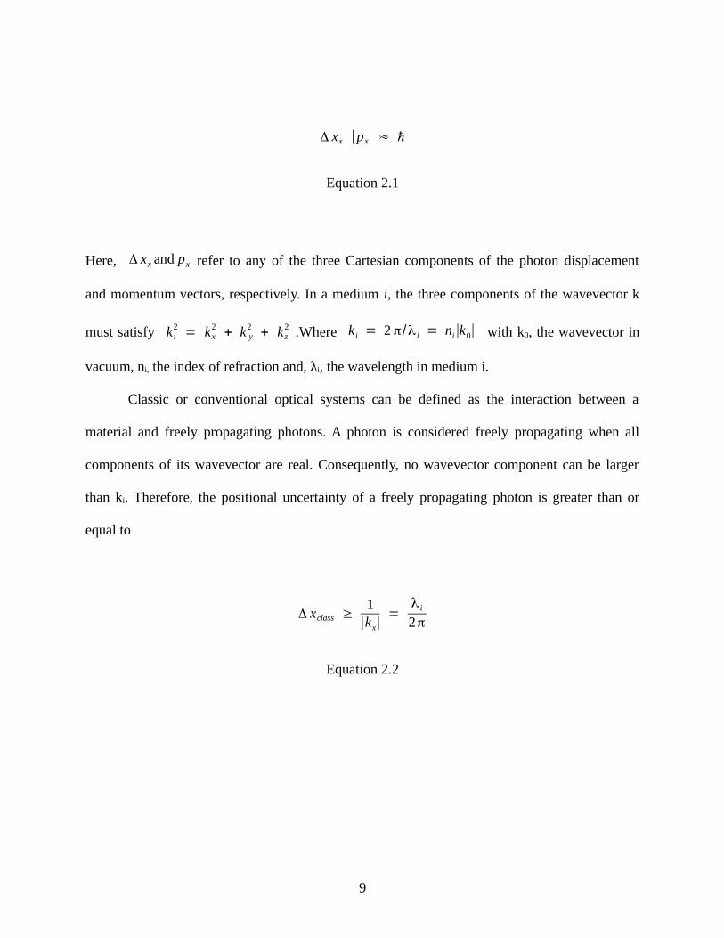
Here, Δ xx and px refer to any of the three Cartesian components of the photon displacement
and momentum vectors, respectively. In a medium i, the three components of the wavevector k
must satisfy k i2= kx
2+ k y
2+ kz
2 .Where k i = 2 π/λ i = ni|k0| with k0, the wavevector in
vacuum, ni, the index of refraction and, λi, the wavelength in medium i.
Classic or conventional optical systems can be defined as the interaction between a
material and freely propagating photons. A photon is considered freely propagating when all
components of its wavevector are real. Consequently, no wavevector component can be larger
than ki. Therefore, the positional uncertainty of a freely propagating photon is greater than or
equal to
9
Δ xx |px| ≈ ℏ
Equation 2.1
Δ xclass ≥1|kx|
=λ i
2π
Equation 2.2
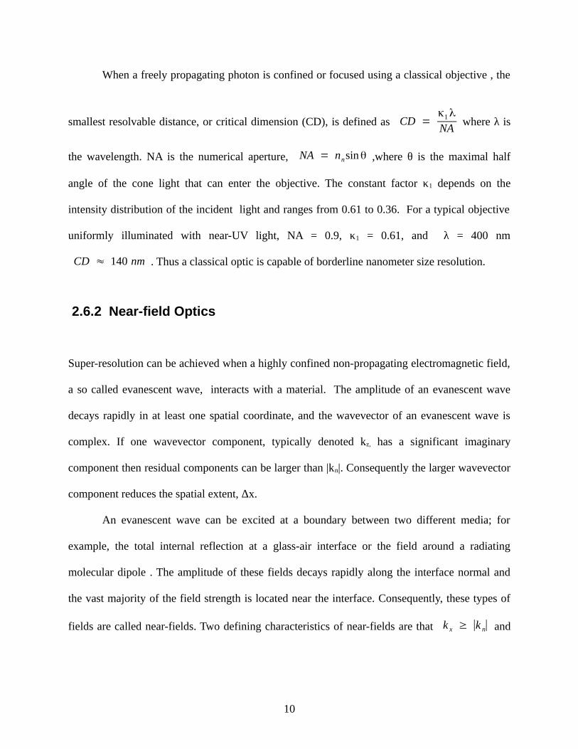
When a freely propagating photon is confined or focused using a classical objective , the
smallest resolvable distance, or critical dimension (CD), is defined as CD =κ1λ
NAwhere λ is
the wavelength. NA is the numerical aperture, NA = nnsinθ ,where θ is the maximal half
angle of the cone light that can enter the objective. The constant factor κ1 depends on the
intensity distribution of the incident light and ranges from 0.61 to 0.36. For a typical objective
uniformly illuminated with near-UV light, NA = 0.9, κ1 = 0.61, and λ = 400 nm
CD ≈ 140 nm . Thus a classical optic is capable of borderline nanometer size resolution.
2.6.2 Near-field Optics
Super-resolution can be achieved when a highly confined non-propagating electromagnetic field,
a so called evanescent wave, interacts with a material. The amplitude of an evanescent wave
decays rapidly in at least one spatial coordinate, and the wavevector of an evanescent wave is
complex. If one wavevector component, typically denoted kz, has a significant imaginary
component then residual components can be larger than |kn|. Consequently the larger wavevector
component reduces the spatial extent, Δx.
An evanescent wave can be excited at a boundary between two different media; for
example, the total internal reflection at a glass-air interface or the field around a radiating
molecular dipole . The amplitude of these fields decays rapidly along the interface normal and
the vast majority of the field strength is located near the interface. Consequently, these types of
fields are called near-fields. Two defining characteristics of near-fields are that k x ≥ |k n| and
10

ε > (8πc)|S| . The first relation is the previously described wavevector equality, and the
second relation shows that the energy density, ε, is greater than the time-averaged flow of
radiation through a volume element determined by the Poynting vector, S. The latter expression
is an equality for freely propagating waves.
2.7 SPECIFIC SPM TECHNIQUES.
Centuries of research has produced rich insights into the fundamental principles which govern
the interaction between electromagnetic fields and matter. Application of this knowledge has
allowed the development of a diverse range of spectroscopic techniques, and highly selective
techniques have emerged which are capable of interrogating a sample to provide information on
the elemental composition, chemical and molecular organization, and higher level structural
information. In the fields of localized probe-based microscopy, a wide array of techniques have
been developed.
2.8 FORCE-DISTANCE CURVES
Static or contact mode atomic force microscopy (AFM) is used to measure the mechanical
properties of a sample and is a well-developed branch of AFM. In contact mode AFM, a
mechanical cantilever probe is scanned above a sample while a detector sensitive to probe
deflection is used to measure the tip-sample force. This method can probe both attractive and
11
repulsive forces. Contact mode AFM is typically operated in the repulsive regime, i.e., the
cantilever is in contact with the surface and is deflected away from the surface. However, static
mode AFM can be operated in both the repulsive and attractive regimes. Static mode is in
reference to the fact that the cantilever is not undergoing dynamic oscillating motion.
The standard application of contact AFM is imaging of surface topography using a
constant force imaging modality. The tip is in direct contact with surface and the tip-surface
interaction is principally a strongly repulsive interaction. Detection of cantilever deflection and a
tip-sample interaction force setpoint are used to parameterize an electronic feedback loop used to
maintain a constant force between the tip and sample. If the spring constant of the probe is
significantly lower than the effective spring constant of the sample atomic bonds, direct
determination of the height of the surface is possible. The contact zone between tip and sample is
typically understood to consist of many atoms; a contact diameter in the range of 1-10 nm is
typical. Long-range attractive tip-sample forces can be imaged using a constant height scanning
motif. For example, if a ferromagnetic probe is used, then magnetic forces domain can be sensed
from the cantilever deflection observed in constant height mode imaging. Friction Force
microscopy is an another static mode AFM technique. By scanning the cantilever sidewise with
respect to the cantilever length in constant-force contact mode, the lateral forces caused by
torsional bending of the cantilever can be detected. Using this signal, local variations in surface
friction can be resolved with nanometer resolution.
Force-distance curves are measured by monotonically decreasing the probe-sample
separation while the cantilever deflection is monitored. It is desirable to obtain the tip-sample
force, Fts(d), as a function of tip-sample distance, d. What is principally measured during the
12
collection of a force distance curve is the deflection of the cantilever tip, z tip, as a function of the
z-position of the sample. Althought the ztip is proportional to Fts(d), the z-position of the sample is
a convolution of the z-motion and the cantilever deflection.
Mechanical properties, such as sample elasticity or maximum tip-sample adhesion force
are readily measured using force-distance curves. Additionally, when imaging samples that are
sensitive to the applied tip-sample force, such as soft biological samples, a force-distance curve
conducted at pre-selected points enables selection of a force setpoint that does not unnecessarily
wear and degrade sample integrity.
2.9 APERTURELESS NEAR-FIELD OPTICAL MICROSCOPY
In the original scanning near-field optical microscope (SNOM), the aperture-based SNOM, the
optical diffraction limit is surpassed by forcing light through the metallic aperture of an optical
fiber-like probe under near-field conditions. By definition, near-field conditions require the probe
to be positioned in close proximity to the surface where near-fields, optical or otherwise, have
significant amplitude. As has been stated previously, the resolution of the optical near-field
scanning probe techniques is limited by the diameter of the probe. Unfortunately, the probe
diameter also limits signal-to-noise as the aperture size shrinks and ultimately reduces the light
throughput. In aperture-based NSOM, the metalized, tapered glass geometry of the probe must
balance miniaturization of the probe dimensions against the photon throughput limitations
imposed by the waveguide cutoff effect.
13

Apetureless near-field scanning optical microscopy (ANSOM) circumvent the aperture-
size paradox by leveraging well-known mechanisms of optical field enhancement. Typically, a
strongly scattering sharp probe, such as an AFM tip, is placed in the focus of a laser beam
allowing field confinement effects to act as the basis of the ultra resolution mechanism. The
nano-optical field in the near-field region of the probe apex can be strongly enhanced due to
localized surface plasmon resonances or to geometric considerations such as lightning rod and
antenna effects.
In general, two classes of ANSOM have emerged. One type is scatter type microscopy (s-
SNOM), in which a strongly scattering tip is either polarized by a surface near-field or polarizes
a surface near-field.[3] In this method the tip scatters the optical near-field, converting it into a
propagating optical signal which can be detected by traditional optical schemes. The second type
is tip enhanced microscopy, where a tip enhanced field is used to locally excite a material by a
variety of optical mechanisms.[6] Mechanisms include: tip enhanced Raman scattering, tip-
enhanced harmonic generation, and tip-enhanced fluorescence. More recently, s-SNOM probes
in which single metal particles are attached to dielectric tips have emerged. [2] This probe
morphology is both significantly more robust and mechanically superior than the high aspect
ratio tip previously used in s-SNOM.
The ANSOM technique used in the studies contained in this thesis are based on sharp tip
light scattering. Again, this technique has no wavelength based resolution limit; resolution is
nearly entirely determined by the probe radius. Probes with 20 nm radii are common and 10 nm
lateral resolutions have been demonstrated.
14
2.10 FUTURE OF SCANNING PROBE MICROSCOPY (SPM)
Central to all SPM techniques is the use of a mechanical tip. A probe located in the near-field of
a sample can sense a diverse spectrum of interaction mechanisms. Simultaneous high resolution
measurement of near-field interaction mechanisms and topography is a major advantage of SPM.
However, SPM techniques have not been fully developed into user-friendly and robust systems,
and are typically limited in scan speed and field of view. Consequently significant efforts need
to be made in:
• The use of multi-probe systems. Multi-probe techniques will increase sample acquisition speed
and interaction volumes. By using an array of tips, it would be possible to sense different
sample properties simultaneously.
• The development of probes which join both sensor and actuator functionality. Possible
examples would include nanoscalpels or nanopipettes. Nanoscale detector arrays will allow a
diverse range of surface properties to be assessed.
• The integration of SPM into complementary microscopy techniques, such as classical optical
microscopes. Integration of SPM, focused ion beam and SEM in a single system would
provide characterization and fabrication possibilities relevant to a wide range of fields.
15

2.11 BIBLIOGRAPHY
[1] Hughes, A. (1956). Studies in the history of microscopy. 2. the later history of the achromatic microscope, Journal of the Royal Microscopical Society 76 : 47-60.
[2] Kalkbrenner, T.; Håkanson, U.; Schädle, A.; Burger, S.; Henkel, C. and Sandoghdar, V. (2005). Optical microscopy via spectral modifications of a nanoantenna, Physical review letters 95 : 200801.
[3] Knoll, B. and Keilmann, F. (1999). Near-field probing of vibrational absorption for chemical microscopy, Nature 399 : 134-137.
[4] Novotny, L. and Hecht, B., 2012. Principles of nano-optics. Cambridge University Press, Cambridge, UK;New York;.
[5] Tendeloo, G. V.; Van Dyck, D. and Pennycook, S. J., 2012. Handbook of nanoscopy. Wiley-VCH, Weinheim, Germany.
[6] Wessel, J. (1985). Surface-enhanced optical microscopy, JOSA B 2 : 1538-1541.
[7] Yablon, D. G., 2013. Scanning probe microscopy for industrial applications: nanomechanical characterization. John Wiley & Sons, Hoboken, New Jersey.
[8] Zayats, A. V. and Richards David, P., 2009. Nano-optics and near-field optical microscopy. Artech House, Boston;London;.
16
3.0 OBSERVATION AND ANALYSIS OF LOCALIZED
OPTICAL SCATTERING WITH NON-PASSIVE PROBES
Author contribution: The author of this dissertation was responsible for all the experiments and
prepared the manuscript.
3.1 INTRODUCTION
Nanophotonics have demonstrated promise in a range of applications from integrated optical
circuits to medical diagnostics.[12; 13; 19; 55; 72; 77; 79; 84] Often, only a
small set of simple, subwavelength structural elements such as concentric circles, slit apertures,
and two dimensional aperture arrays are utilized to construct complex nanophotonic devices.
[12; 13; 17; 19; 24; 46; 47; 56] The increasing sophistication of nanophotonics
depends on an acute understanding of the interaction between electromagnetic radiation and
these subwavelength optical elements. Direct observation of this interaction is possible with the
use of a near-field scanning microscope. Near-field scanning microscopy is capable of resolving
electromagnetic phenomenon at length scales below the diffraction limit.[3; 5; 23; 27;
29; 31; 32; 35-38; 42; 43; 58; 66; 68; 78; 81; 86] However, several
17
well documented experimental challenges, convolute the signal response of near-field
microscopes.[8; 23; 29; 35; 42; 54; 58; 66] In this work, transmission mode
apertureless near-field scanning optical microscopy is employed to study localized optical
scattering above a subwavelength aperture. This document will address complexities arising
from the interaction of propagating radiation with a polarizable probe-sample interface.
The term scanning near-field optical microscope (NSOM) is used to describe members of
a family of instruments capable of resolving electromagnetic field distributions at length scales
significantly smaller than the diffraction limit. The maximum resolution of traditional optical
microscopes utilizing diffraction limited optics approaches λ/2, where λ is the wavelength of
illumination.[67] NSOM studies regularly demonstrate resolutions of λ/10 and λ/60 resolution
has been reported.[61]
The NSOM was first proposed in 1928 by E.H. Synge.[74] In a brief series of papers
and private correspondences exploring the feasibility of sub-wavelength resolution, Synge
proposed a mechanism of image formation using an optical probe consisting of a sub-wavelength
circular aperture in an opaque screen or a quartz cone with a metal coating everywhere except
the apex. Illumination of these sub-wavelength apertures generates an electromagnetic near-field
containing high spatial frequency components. Placing a sample surface into the generated near-
field facilitates scattering of high spatial frequency fields by sub-wavelength size surface
elements. Scanning the aperture in a plane parallel to the sample surface and collecting scattered
light with diffractive optics generates a super-resolved image. Spatial resolution is due to the
localized nature of the electromagnetic near-field. Efficient near-field to far-field conversion is
possible only when the separation between aperture and sample is less than the wavelength of the
incident field. When optical frequency illumination sources are used, nanometer scale resolution
18

may be obtained; however, distance regulation on the order of several 10s of angstroms is
required. The significant technological challenges imposed by nanometer scale scanning resulted
in a significant delay before Synge’s hypothesis was verified at optical frequencies. By 1984,
rapid development of piezoelectric crystal fabrication and scanning probe microscopy (SPM)
techniques such as scanning tunneling microscopy and atomic force microscopy (AFM)
facilitated experimental verification of NSOM in the visible spectrum.[61] More recently,
several research groups have obtained sub-wavelength resolved images by scattering high spatial
frequency fields with a subwavelength spherical probe.[7; 32; 86] Near-field scanning
techniques based on this approach are generally referred to as apertureless NSOM or ANSOM.
Several review articles focusing on aperture based NSOM [10; 16], ANSOM [31; 33;
58], and optical near-field theories [21; 60] demonstrate the development this field.
ANSOM overcomes several significant experimental limitations of aperture based
NSOM such as:
• Skin depth limited resolution
• In visible spectrum NSOM, maximum resolution approaches 20 nm due to the skin depth of
metals used to define the aperture boundary.
• Low signal sensitivity
• Small signal levels are due to inherently small light throughput of the aperture.
• Low incident power
• Near-field illumination intensity is limited by thermal damage mechanisms present at probe
apertures
• Waveguide cut off
19

• NSOM probes are typically constructed by from elongated optical waveguides.
Consequently, the utility of aperture NSOM is limited to wavelengths below the cut-off
frequency.[3; 9; 23; 25-29; 32-34; 54; 65; 85]
In ANSOM, near-field resolution is proportional to the spatial profile of the probe. The
radius of curvature at the apex of commercially available SPM probes commonly approach 5 nm.
ANSOM signal sensitivity can be enhanced by utilizing probe materials with large scattering or
absorption cross section. Metal coated probes have radius of curvature approaching 25nm. A
single ANSOM system may be utilized across broad spectral range.[29] The widespread
availability of commercial probes and probe positioning equipment significantly enhances the
accessibility of ANSOM as a common laboratory instrument.
As with all scanning probe technologies, the key physical principles involved are
localized in the region surrounding the probe. Of primary importance is the physics of probe-
sample optical coupling. In ANSOM experiments, sensitivity and resolution critically depend on
the ability of the probe-sample systems to localize and scatter electromagnetic fields with large
spatial wavevectors, ksp. Typically, an ANSOM probe is placed between one and several hundred
nanometers above the sample surface. At this length scale, theoretical calculations predict
enhancement of incident electromagnetic fields at optical frequencies for many materials.
Additional field enhancement is expected for systems which support surface active
electromagnetic resonance modes such as plasmons or phonons.[4; 30; 40; 63] Also, the
“lightning rod effect,” present in all geometrically constrained conductive systems, plays a role
in localized field enhancement.[11; 18; 50; 62]
20
Theoretical probe-sample coupling studies have been reported using a multitude of
techniques. These techniques include the multiple-multipole method [11; 53; 56; 63], the
Green dyadic technique[21; 22; 40; 59], the Finite Difference Time Doman [51] , and
rigorous electromagnetic treatments [6; 15; 62; 78] .
A primary challenge of ANSOM experiments arises from the need to isolate true optical
near-field signals, which contributes a small fraction to the total collected signal. Background
contributions from light reflected, scattered, or diffracted by nearby sample structures often
masks the localized probe-sample coupling and diminishes resolution. Two techniques, Lock-in
amplification [43; 78] and high harmonic demodulation [29; 39; 42; 70] are often
used to overcome this issue. These techniques may be implemented via harmonic modulation of
the probe sample separation. In ANSOM experiments, probe-sample distances are frequently
regulated by an AFM controller capable of performing non-contact or “tapping mode” (TM)
imaging [10; 64].
This work reports the characterization of near-field optical properties of elementary
structures. Apertureless scanning near-field optical microscopy (ANSOM) enables observation of
optical properties below the diffraction limit; however, data collected by this technique may
contain more than near-field contributions. In this work, transmission mode ANSOM is used to
study optical properties of an isolated subwavelength slit. Constant-height mode ANSOM images
reveal fringe patterns on both sides of a slit aperture. Fringe patterns are sensitive to the relative
positions of the ANSOM detection optics and the slit. Fringes result from a superposition of
probe scattered fields and the average wavevector of collected light. Analysis confirms the
existence of two families of scattered fields which are directed parallel to the sample plane and
21

propagate in opposite directions away from the slit. Data collected using different probe
geometries reveal the existence of a homodyning field comprised of fields transmitted through
the slit and scattered by the ANSOM probe body.
3.2 EXPERIMENTAL DETAILS
3.2.1 Deposition of Metal Film
An Electron-beam evaporation system (Thermionics model VE 180) was used to evaporate a
200nm thick Au film over a 5 nm layer of Ti on a quartz substrate. Prior to metal film deposition,
the substrate was cleaned in argon plasma.
3.2.2 Fabrication of Nanoslits
A focused ion/electron dual beam system (JEOL model SMI-3050SE) was used to mill apertures
into the metal film. An ion beam with 100 pA current was used. The minimum ion dose required
to completely mill through the metal film was determined by milling and cross-sectioning
several test structures in a manner similar to that recently reported.[57]
22
3.2.3 Near-field Microscopy
In order to study sub-wavelength resolved optical fields localized near the surface of isolated
apertures, an ANSOM was designed and constructed. The ANSOM was constructed by
integrating a sample illumination pathway and a homebuilt optical microscope into a commercial
SPM platform (Veeco Instruments, Dimension 3100). A brief description of the experimental
apparatus follows.
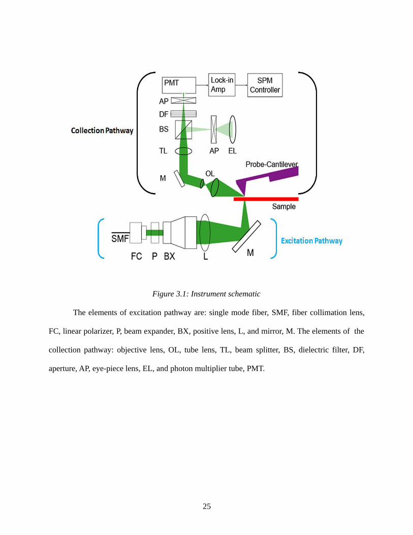
Direct backside illumination of sample structures was achieved with a sample excitation
pathway and a custom SPM sample stage (Figure 3.1). A single mode, polarization maintaining
optical fiber coupled 532 nm light from frequency doubled Nd:YVO4 laser into the excitation
pathway. Fiber optic output was collimated by an aspherical lens and passed through a linear
polarizer. Incident field polarization angle was set by rotating the major axes of the fiber and the
polarizer. The electric component of the incident field was polarized perpendicular to the long
axis of the slit. A reversed telescope expanded the collimated beam diameter to match the input
iris of a condenser lens. A 45 degree mirror directed the focused Gaussian beam onto the
backside of the patterned metal film. A portion of the fields transmitted and diffracted by the slit
aperture were scattered by an oscillating probe and collected using 10x long working distance
objective lens, NA = .23, elevated approximately 15 degrees above the x-y sample plane. The
objective was focused onto the SPM probe/nanoaperture interaction zone. A dielectric filter
separated incident illumination and 670 nm wavelength SPM feedback illumination. An
adjustable aperture placed in a confocal plane helped limit collected scattering to a region several
microns wide centered near the probe apex. Light passing through the aperture impinged onto a
photon multiplier tube (Hamamatsu 1P28). PMT signals were passed to an impendence matched
23

input of a lock-in amplifier (Stanford Research SR844). Cantilever-probe oscillation frequencies,
obtained from the SPM controller electronics, provided the lock-in reference signal.
Demodulated optical signals were routed to the SPM controller, synchronized to SPM
topography and stored.
24
25
Figure 3.1: Instrument schematic
The elements of excitation pathway are: single mode fiber, SMF, fiber collimation lens,
FC, linear polarizer, P, beam expander, BX, positive lens, L, and mirror, M. The elements of the
collection pathway: objective lens, OL, tube lens, TL, beam splitter, BS, dielectric filter, DF,
aperture, AP, eye-piece lens, EL, and photon multiplier tube, PMT.

ANSOM images were collected by laterally scanning a SPM probe regulated by TM
feedback. In order to minimize optical-topographical coupling, ANSOM data was collected at a
constant height above the average sample plane. [42] PtIr5 coated conductive SPM probes
with an approximate force constant between 42-45 N/m, were used in all studies. Peak to center
probe oscillation amplitude was set to approximately 85nm. Two different apertureless probe
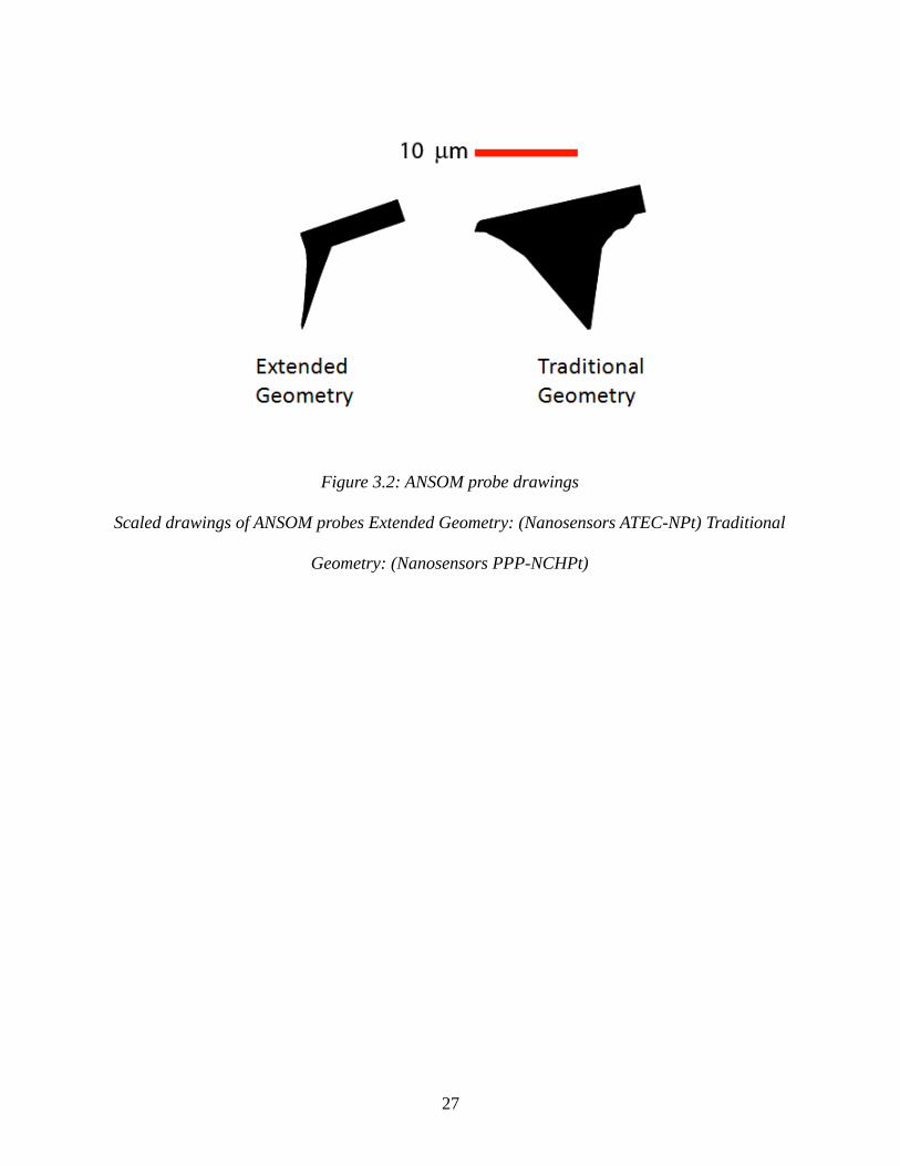
geometries were utilized in this study. Scaled drawings of the traditional geometry (Nanosensors
PPP-NCHPt) and extended geometry (Nanosensors ATEC-NPt) probes used in this study are
depicted in (Figure 3.2).
26
27
Figure 3.2: ANSOM probe drawings
Scaled drawings of ANSOM probes Extended Geometry: (Nanosensors ATEC-NPt) Traditional
Geometry: (Nanosensors PPP-NCHPt)

3.3 RESULTS AND DISCUSSION
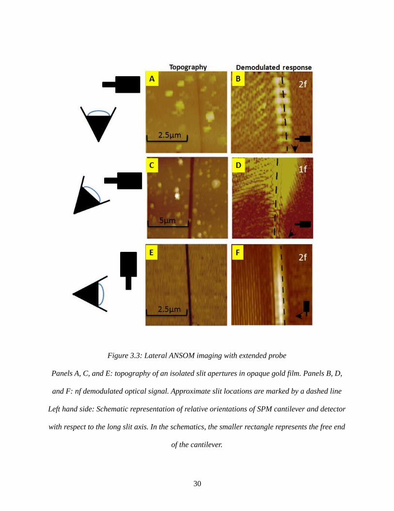
3.3.1 Lateral ANSOM Images of a Single Metallic Nanoslit
We present three cases where changes in the relative orientations of the detector and probe-
cantilever system with respect to a slit aperture affect fringe patterns observed in ANSOM
images. In (Figure 3.3), panels A, C, and E display topography of an isolated slit aperture in
opaque gold film. Panels B, D, and F display constant height n f demodulated optical signals.
Approximate slit locations are marked by a dashed line. On the left hand side of this figure,
relative orientations of the SPM cantilever and detector with respect to the long slit axis are
represented schematically. In the schematics, the smaller rectangle represents the free end of the
cantilever.
In the first case, (Figure 3.3 A, B) the detector is parallel to the slit, looking down the
long slit axis, and tilted 15degrees above the sample plane. The fringe pattern observed in the 2f
demodulated optical signal makes angles of +/- 45 degrees from the long slit axis, with the
fringes on either side of the slit being perpendicular to each other. The demodulated optical
image shows a clear asymmetry in the field amplitudes on each side of the slit, with the fringes
on the left side being far more pronounced than those on the right. Preliminary results, discussed
in a subsequent section, suggest that this asymmetry arises from the cantilever’s orientation with
respect to the slit.
28
In the second case, (Figure 3.3 C, D) the slit remains in roughly the same orientation as
the first case, but the detector is now rotated clockwise by 45 degrees. The fringe pattern
observed in the 1f demodulated signal also appears to rotate clockwise relative to the first case,
with the fringes on either side remaining mutually orthogonal. Again, asymmetric intensity
distribution on either side of the slit is observed. However in this case, the gain on the detector
was increased making the fringes on the right hand side more apparent and in turn causing
detector saturation in higher intensity regions.
In the third case, (Figure 3.3 E, F), the sample and SPM scan angle are rotated 90 degrees
in the laboratory frame. These rotations produce qualitatively similar topography as compared to
the previous cases, but the key difference here being the slit is now oriented perpendicular to the
detector. Fringing is exclusively observed on one side of the slit.
29
30
Figure 3.3: Lateral ANSOM imaging with extended probe
Panels A, C, and E: topography of an isolated slit apertures in opaque gold film. Panels B, D,
and F: nf demodulated optical signal. Approximate slit locations are marked by a dashed line
Left hand side: Schematic representation of relative orientations of SPM cantilever and detector
with respect to the long slit axis. In the schematics, the smaller rectangle represents the free end
of the cantilever.
3.3.2 Model: Superposition of Background and Probe Scattered
Fields
In this section a model based on the approach of Aubert [5] is expanded and utilized to explain
interference patterns observed in lateral ANSOM images. This model accurately predicts
observed fringe periodicity and two-dimensional interference profiles.
Illumination of a stationary nanoslit milled in an optically thick metal screen leads to
diffraction causing a static background field. When losses due to specular scattering by the metal
film and material absorption are neglected this field can be expressed as
Ediff =|Ediff|exp (i φ diff )
Equation 3.1
where φdiff is the phase of the diffracted reference field. A conductive spherical probe
scanned a distance z above the x-y sample plane scatters a portion of the diffracted field. The
field scattered by a harmonically oscillating probe is given by
Et =|E t|exp (iφ t (x , y , t))
Equation 3.2
31
where φt is the position-sensitive phase of the scattered field. Field perturbations due to probe
motion along the z-axis may be neglected if the probe is smaller than the incident wavelength
and the distance between the sample and probe is constant [42]. Setting the reference signal of
a lock-in amplifier to the probe oscillation frequency facilitates detection of probe modulated
fields. Elimination of non-modulated intensity products of ( Et+ Ediff )2 allows the intensity to be
expressed as
I ( x , y , t )=|Et|2+2|Ediff E t|cos (φt(x , y)+φdiff )
Equation 3.3
Theoretical [2; 14; 20; 41; 42; 44; 45; 48; 49; 52; 69; 75; 76;
80; 82] and experimental [1; 2; 20; 73; 80; 83] studies have suggested that the
edges of a sub-wavelength slit transform incident fields into transmitted fields containing
wavevector components parallel to the metal film output surface. In this case, transmitted fields
propagate away from the center of the slit, and the plane containing the long slit axis and the z-
axis forms a plane of symmetry. φt may be expressed as
φt (x , y )=k diff ∙ (x X+ y Y )−kdet ∙ ( x X+ y Y )
Equation 3.4
32
where kdiff is the wavevector of the diffracted portion of the transmitted field, and kdet is
the average wavevector admitted by the objective lens. X and Y are Cartesian unit vectors
which describe the sample plane. Only the components of the kdiff and kdet parallel to the sample
surface are included in Equation 3.4. In order to account for the proposed diffraction symmetry,
Equation 3.4 is re-expressed as
φ t (x , y )= (−1)ζ k diff [ x cos (θs−π2)+ y sin(θs−
π2)]−kdet⋅( x X+ y Y )
Equation 3.5
with
ζ = 0 if angle(x , y )<θs
1 if angle(x , y )>θs
Equation 3.6
The function “angle(x,y)” returns the angle from the x-axis to a line containing the origin
and the probe location. Probe coordinates directly overlapping the slit aperture are neglected.
Inserting Equation 3.5 into Equation 3.3 permits calculation of two dimensional, probe-position
dependent interference plots.
This model predicts that the direction of the fringe pattern can be controlled by either
rotating the detector relative to the diffracted field, or vice versa. Namely, it is the direction of
the average detected wavevector, kdet, relative to the diffracted wavevector, kdiff, that determines
33
the angle of the fringes through Equation 3.5. In order for the fringes on the left and right to
remain orthogonal to each other during rotation of the detector, they must result from the
superposition of wavevectors with identical magnitudes.
Simulated phases corresponding to the three case geometries discussed were calculated
and are presented in (Figure 3.4 B, D, F). The directions of kdet and kdiff used in these simulations
are indicated by white vectors. Simulated interference patterns are consistent with the collected
demodulated optical scattering images shown in (Figure 3.4 A, C, E). Simulated fringe patterns
were calculated by assuming diffracted wavevectors possess significant projections along plane
of the metal film and, on each side of the aperture, diffracted fields propagate in opposite
directions. In the first two cases, panels A-B and C-D, fringes on either side of the slit are
perpendicular to each other. In the third case (Figure 3.4 E, F), where the slit is perpendicular to
the detector, the model predicts the absence of fringes, right hand side of panel F, due to
antiparallel alignment of detected wavevectors.
34
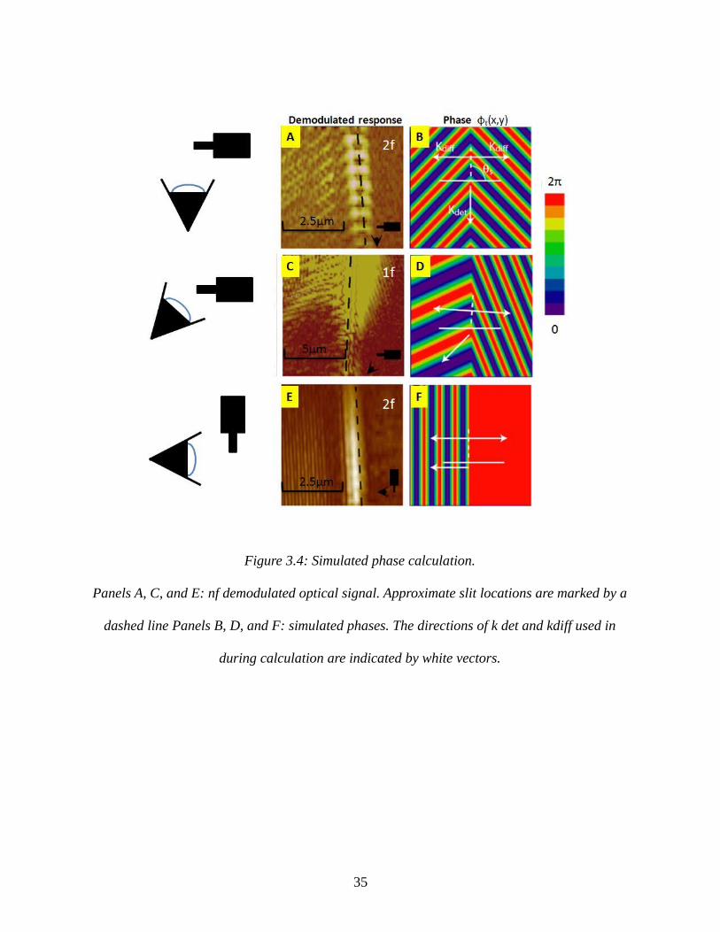
35
Figure 3.4: Simulated phase calculation.
Panels A, C, and E: nf demodulated optical signal. Approximate slit locations are marked by a
dashed line Panels B, D, and F: simulated phases. The directions of k det and kdiff used in
during calculation are indicated by white vectors.

This model fails to address origins of the asymmetry observed in the measured field
intensities on the two sides of the slit. This is because the interference model only accounts for
probe position and does not consider complex probe shape. A comparison of ANSOM images
collected with different styles of SPM probe geometries sheds light upon the origin of
asymmetric intensity.
ANSOM images presented in (Figure 3.5) were collected with traditional geometry
probes whereas the images contained in (Figure 3.4) were collected using extended geometry
probes. When a traditional probe is scanned on the right side of the slit, propagating light
transmitted directly through the apertures is reflected off of the base of the probe and the end of
the cantilever, creating a strong self-homodyning field [71]. In panel B of (Figure 3.5), this
constructive interference results in the high intensity vertical band located to the right of the slit.
On the other hand, when the probe is scanned over the left side of the slit, the transmitted field is
reflected weakly off of the base of the cantilever resulting in a smaller homodyned field.
Increasing detector gain allows observation of scattered field on the left side (data not shown) at
the expense of detector saturation. A comparison of the adjacent scattering surfaces available
when a probe is located on left and right hand sides of the slit is illustrated in (Figure 3.6).
36

37
Figure 3.5: ANSOM imaging with traditional probe
Panel A: topography signal Panel B: 1f demodulated optical signal Panel C: 2f demodulated
optical signal In these images, the relative orientation of SPM cantilever and detector with
respect to the long slit axis is comparable to the experimental geometry depicted in (Figure 8
A,B).
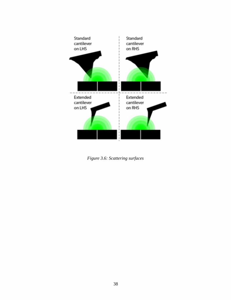
38
Figure 3.6: Scattering surfaces
Replacement of a traditional geometry probe with an extended geometry probe requires
an increase in the detector gain. In the images collected with the extended probe, (Figure 3.4),
fringes are predominantly observed left of the slit. Additional increases in detector gain allow
observation of fringes on the right side while saturating the detector elsewhere. When the
extended probe is on the left side, reflection of transmitted fields is qualitatively similar to the
situation in which the traditional probe is located left of the slit. Compared to traditional probes,
extended probes posses smaller surface area which may explain the increased detector gain.
Extended probe bodies weakly scatter the transmitted fields and produce a relatively weak self-
homodyning field.
When the extended probe is located right the slit, there is a low probability that the
cantilever body or tip base can scatter transmitted light, and detector gain must be significantly
increased to observe fringing right of the slit. For traditional tips located right of the aperture,
portions of tip base and cantilever body protrude towards the slit. This may be the cause of the
high intensity strip observed right of the slit in (Figure 3.5 B).
At 2f demodulation, (Figure 3.5 C), fringe patterns were diminished and intensity more
localized near slit edges than in the 1f demodulation image (Figure 3.5 B). 2f demodulated
signals are more sensitive to surface bound fields [29]; this suggests a majority of the light
exiting the slit apertures is weakly bound to the sample surface.
The experimentally observed interference originates from variations in optical path length
between the probe and detector. The existence of fringes in regions several wavelengths away
from the aperture edges suggests the presence of freely propagating background fields. The ratio
of scattered far-fields to scattered near-fields, e.g. fields localized along the edges of the slit, is
large. Consequently, resolution of near-fields launched and scattered by the subwavelength
39

dimensionality of this aperture requires a higher degree of far-field discrimination than was
achieved in this study. Improvements in near-field to far-field scattering ratio can be obtained
several ways. Demodulation at frequencies greater than 2f would result in images containing
higher concentration of localized fields; however, advantages of higher harmonic demodulation
are partially offset by decreases in overall signal intensity. Because the slit aperture utilized in
this study was not strictly sub-wavelength, a non-negligible portion of incident field was able to
propagate through the aperture. Fabrication of apertures with larger depth to width aspect ratios,
possible with lower ion beam currents, or illumination with longer wavelength incident fields
would significantly decrease contributions of this field to the total signal. Additionally, with the
probe’s apex near the surface, a large number of scattering centers along the base of the tip and
cantilever body exist outside of the near-field intensity region. The scattering contributions of
these centers likely originate in the far-field and do not enhance image resolution. The surface of
an ideally suited probe would be optically passive at every except at the apex. Selective etching
or deposition of conductive SPM probes may provide additional signal to noise enhancement.
3.4 SUMMARY AND CONCLUSIONS
We demonstrated ANSOM images of a nanoslit aperture contain interference fringes which result
from superposition of the average detected wavevector and components of the field scattered by
the nanoslit. Analysis confirms that such a slit generates two scattered orders launched
perpendicular to the slit. Furthermore, fringe patterns can be controlled by changing the
orientation of the slit, and thus the direction of the two scattered orders, with respect to the
40

detector or vice versa. The model originally developed by Aubert et al. was extended to account
for the two scattered orders present in our system. The resulting calculated fields agreed well
with the ANSOM data in several different detector/slit orientations.
Additionally, probe geometry and probe position relative to the slit strongly affect the
magnitude of self-homodyning fields exhibited in ANSOM images. For a single slit aperture,
sources of homodyning fields include a propagating field transmitted through the slit and
reflected by the probe base and/or cantilever body. Sensitivity of self-homodyne amplification to
probe geometry suggests that portions of the probe base and cantilever body scatter significant
transmitted optical fields.
41
3.5 BIBLIOGRAPHY
[1] Aigouy, L.; Lalanne, P.; Hugonin, J. P.; Julie, G.; Mathet, V. and Mortier, M. (2007). Near-Field analysis of surface waves launched at nanoslit apertures, Physical Review Letters 98 : 153902/1-153902/4.
[2] Akarca-Biyikli, S. S.; Bulu, I. and Ozbay, E. (2004). Enhanced transmission of microwave radiation in one-dimensional metallic gratings with subwavelength aperture, Applied Physics Letters 85 : 1098-1100.
[3] Akhremitchev, B. B.; Pollack, S. and Walker, G. C. (2001). Apertureless scanning near-field infrared microscopy of a rough polymeric surface, Langmuir 17 : 2774-2781.
[4] Ashino, M. and Ohtsu, M. (1998). Fabrication and evaluation of a localized plasmon resonance probe for near-field optical microscopy/spectroscopy, Applied Physics Letters 72 : 1299-1301.
[5] Aubert, S.; Bruyant, A.; Blaize, S.; Bachelot, R.; Lerondel, G.; Hudlet, S. and Royer, P. (2003). Analysis of the interferometric effect of the background light in apertureless scanning near-field optical microscopy, Journal of the Optical Society of America B 20 : 2117-2124.
[6] Averbukh, I. S.; Chernobrod, B. M.; Sedletsky, O. A. and Prior, Y. (2000). Coherent near field optical microscopy, Optics Communications 174 : 33-41.
[7] Bachelot, R.; Gleyzes, P. and Boccara, A. C. (1995). Near-field optical microscope based on local perturbation of a diffraction spot, Opt. Lett 20 : 1924-1926.
[8] Barchiesi, D. (2006). Scanning near-field optical data contrast measurement: a tomographylike near-field reconstruction, Appl Opt FIELD Full Journal Title:Applied optics 45 : 7597-601.
[9] Bek, A.; Vogelgesang, R. and Kern, K. (2006). Apertureless scanning near field optical microscope with sub-10 nm resolution, Review of Scientific Instruments 77 : 043703.
[10] Betzig, E. and Trautman, J. K. (1992). Near-field optics: microscopy, spectroscopy, and surface modification beyond the diffraction limit, Science (Washington, DC, United States) 257 : 189-95.
[11] Bohn, J. L.; Nesbitt, D. J. and Gallagher, A. (2001). Field enhancement in apertureless near-field scanning optical microscopy, J. Opt. Soc. Am. A 18 : 2998-3006.
42
[12] Bonod, N.; Popov, E.; Li, L. and Chernov, B. (2007). Unidirectional excitation of surface plasmons by slanted gratings, Optics Express 15 : 11427-11432.
[13] Bozhevolnyi, S. I.; Volkov, V. S.; Devaux, E.; Laluet, J.-Y. and Ebbesen, T. W. (2006). Channel plasmon subwavelength waveguide components including interferometers and ring resonators, Nature (London, United Kingdom) 440 : 508-511.
[14] Bravo-Abad, J.; Martín-Moreno, L. and García-Vidal, F. J. (2004). Transmission properties of a single metallic slit: From the subwavelength regime to the geometrical-optics limit, Physical Review E 69 : 26601.
[15] Calander, N. and Willander, M. (2002). Theory of surface-plasmon resonance optical-field enhancement at prolate spheroids, Journal of Applied Physics 92 : 4878-4884.
[16] Dunn, R. C. (1999). Near-Field scanning optical microscopy, Chemical Reviews (Washington, D. C.) 99 : 2891-2927.
[17] Egorov, D.; Dennis, B. S.; Blumberg, G. and Haftel, M. I. (2004). Two-dimensional control of surface plasmons and directional beaming from arrays of subwavelength apertures, Phys. Rev. B 70 : 033404.
[18] Furukawa, H. and Kawata, S. (1996). Analysis of image formation in a near-field scanning optical microscope: effects of multiple scattering, Optics Communications 132 : 170-178.
[19] Gan, Q.; Guo, B.; Song, G.; Chen, L.; Fu, Z.; Ding, Y. J. and Bartoli, F. J. (2007). Plasmonic surface-wave splitter, Applied Physics Letters 90 : 161130/1-161130/3.
[20] Garcia-Vidal, F. J.; Lezec, H. J.; Ebbesen, T. W. and Martin-Moreno, L. (2003). Multiple paths to enhance optical transmission through a subwavelength slit, Phys. Rev. Lett. 90 : 213901.
[21] Girard, C. and Dereux, A. (1996). Near-field optics theories, Reports on Progress in Physics 59 : 657-699.
[22] Girard, C.; Martin, O. J. F. and Dereux, A. (1995). Molecular lifetime changes induced by nanometer scale optical fields, Physical Review Letters 75 : 3098.
[23] Gomez, L.; Bachelot, R.; Bouhelier, A.; Wiederrecht, G. P.; Chang, S.-h.; Gray, S. K.; Hua, F.; Jeon, S.; Rogers, J. A.; Castro, M. E.; Blaize, S.; Stefanon, I.; Lerondel, G. and Royer, P. (2006). Apertureless scanning near-field optical microscopy: a comparison between homodyne and heterodyne approaches, Journal of the Optical Society of America B: Optical Physics 23 : 823-833.
[24] Gonzalez, M. U.; Weeber, J. C.; Baudrion, A. L.; Dereux, A.; Stepanov, A. L.; Krenn, J. R.; Devaux, E. and Ebbesen, T. W. (2006). Design, near-field characterization, and modeling of 45 degree surface-plasmon Bragg mirrors, Physical Review B: Condensed Matter and Materials Physics 73 : 155416/1-155416/13.
43
[25] Hayazawa, N.; Inouye, Y. and Kawata, S. (1999). Evanescent field excitation and measurement of dye fluorescence in a metallic probe near-field scanning optical microscope, Journal of Microscopy (Oxford) 194 : 472-476.
[26] Hayazawa, N.; Inouye, Y.; Sekkat, Z. and Kawata, S. (2000). Metallized tip amplification of near-field Raman scattering, Optics Communications 183 : 333-336.
[27] Hecht, B.; Bielefeldt, H.; Inouye, Y. and Pohl, D. W. (1997). Facts and artifacts in near-field optical microscopy, Journal of Applied Physics 81 : 2492-2498.
[28] Hillenbrand, R. and Keilmann, F. (2002). Material-specific mapping of metal/semiconductor/dielectric nanosystems at 10 nm resolution by backscattering near-field optical microscopy, Applied Physics Letters 80 : 25-27.
[29] Hillenbrand, R.; Knoll, B. and Keilmann, F. (2001). Pure optical contrast in scattering-type scanning near-field microscopy, Journal of Microscopy (Oxford, United Kingdom) 202 : 77-83.
[30] Hillenbrand, R.; Taubner, T. and Keilmann, F. (2002). Phonon-enhanced light-matter interaction at the nanometre scale, Nature (London, United Kingdom) 418 : 159-162.
[31] Inouye, Y. (2001). Apertureless metallic probes for near-field microscopy, Topics in Applied Physics 81 : 29-48.
[32] Inouye, Y. and Kawata, S. (1994). Near-field scanning optical microscope with a metallic probe tip, Opt. Lett 19 : 159-161.
[33] Kawata, S. (2001). Near-field microscope probes utilizing surface plasmon polaritons, Topics in Applied Physics 81 : 15-27.
[34] Kawata, S. and Inouye, Y. (1995). Scanning probe optical microscopy using a metallic probe tip, Ultramicroscopy 57 : 313.
[35] Keilmann, F. (2004). Scattering-type near-field optical microscopy, Journal of Electron Microscopy 53 : 187-192.
[36] Kim, Z. H.; Liu, B. and Leone, S. R. (2005). Nanometer-scale optical imaging of epitaxially grown GaN and InN islands using apertureless near-field microscopy, Journal of Physical Chemistry B 109 : 8503-8508.
[37] Knoll, B. and Keilmann, F. (1999). Near-field probing of vibrational absorption for chemical microscopy, Nature (London) 399 : 134-137.
[38] Knoll, B. and Keilmann, F. (2000). Enhanced dielectric contrast in scattering-type scanning near-field optical microscopy, Optics Communications 182 : 321-328.
[39] Konopsky, V. N. (2000). Operation of scanning plasmon near-field microscope with gold and silver tips in tapping mode: demonstration of subtip resolution, Optics Communications 185 : 83-93.
44

[40] Kottmann, J. P.; Martin, O. J. F.; Smith, D. R. and Schultz, S. (2001). Dramatic localized electromagnetic enhancement in plasmon resonant nanowires, Chemical Physics Letters 341 : 1-6.
[41] Kukhlevsky, S. V.; Mechler, M.; Samek, O. and Janssens, K. (2006). Analytical model of the enhanced light transmission through subwavelength metal slits: Green’s function formalism versus Rayleigh’s expansion, Applied Physics B: Lasers and Optics 84 : 19-24.
[42] Labardi, M.; Patane, S. and Allegrini, M. (2000). Artifact-free near-field optical imaging by apertureless microscopy, Applied Physics Letters 77 : 621-623.
[43] Laddada, R.; Benrezzak, S.; Adam, P. M.; Viardot, G.; Bijeon, J. L. and Royer, P. (1999). Detection of an evanescent field scattered by silicon tips in an apertureless scanning near-field optical microscope, European Physical Journal: Applied Physics 6 : 171-178.
[44] Lalanne, P.; Hugonin, J. P. and Rodier, J. C. (2005). Theory of surface plasmon generation at nanoslit apertures, Physical Review Letters 95 : 263902.
[45] Lalanne, P.; Hugonin, J. P. and Rodier, J. C. (2006). Approximate model for surface-plasmon generation at slit apertures, J. Opt. Soc. Am. A 23 : 1608-1615.
[46] Laux, E.; Genet, C.; Skauli, T. and Ebbesen, T. W. (2008). Plasmonic photon sorters for spectral and polarimetric imaging, Nat Photon 2 : 161-164.
[47] Lezec, H. J. (2002). Beaming light from a subwavelength aperture, Science 297 : 820.
[48] Lezec, H. J. and Thio, T. (2004). Diffracted evanescent wave model for enhanced and suppressed optical transmission through subwavelength hole arrays, OPTICS EXPRESS 12 : 3629-3651.
[49] Lindberg, J.; Lindfors, K.; Setälä, T.; Kaivola, M. and Friberg, A. (2004). Spectral analysis of resonant transmission of light through a single sub-wavelength slit, Opt. Express 12 : 623-632.
[50] Martin, O. J. F. and Girard, C. (1997). Controlling and tuning strong optical field gradients at a local probe microscope tip apex, Applied Physics Letters 70 : 705-707.
[51] Martin, Y. C.; Hamann, H. F. and Wickramasinghe, H. K. (2001). Strength of the electric field in apertureless near-field optical microscopy, Journal of Applied Physics 89 : 5774.
[52] Mechler, M.; Samek, O. and Kukhlevsky, S. V. (2007). Enhanced transmission and reflection of few-cycle pulses by a single slit, Physical Review Letters 98 : 163901-4.
[53] Novotny, L. (1996). Single molecule fluorescence in inhomogeneous environments, Applied Physics Letters 69 : 3806-3808.
[54] Novotny, L. and Stranick, S. J. (2006). Near-field optical microscopy and spectroscopy with pointed probes, Annual Review of Physical Chemistry 57 : 303-331.
45

[55] Ohtsu, M.; Kobayashi, K.; Kawazoe, T.; Sangu, S. and Yatsui, T. (2002). Nanophotonics: Design, fabrication, and operation of nanometric devices using optical near fields, IEEE Journal of Selected Topics in Quantum Electronics 8 : 839-862.
[56] Pacifici, D.; Lezec, H. J. and Atwater, H. A. (2007). All-optical modulation by plasmonic excitation of CdSe quantum dots, Nat Photon 1 : 402-406.
[57] Pang, Y.; Genet, C. and Ebbesen, T. W. (2007). Optical transmission through subwavelength slit apertures in metallic films, Optics Communications 280 : 10-15.
[58] Patanè, S.; Gucciardi, P. G.; Labardi, M. and Allegrini, M. (2004). Apertureless near-field optical microscopy, RIVISTA DEL NUOVO CIMENTO 27.
[59] Pieruccini, M.; Savasta, S.; Girlanda, R.; Iotti, R. C. and Rossi, F. (2003). Near-field light emission from nano- and micrometric complex structures, Applied Physics Letters 83 : 2480-2482.
[60] Pohl, D. W. (2001). Near-field optics and the surface plasmon polariton, Topics in Applied Physics 81 : 1-13.
[61] Pohl, D. W.; Denk, W. and Lanz, M. (1984). Optical stethoscopy: Image recording with resolution lambda/20, Applied Physics Letters 44 : 651-653.
[62] Porto, J. A.; Carminati, R. and Greffet, J. J. (2000). Theory of electromagnetic field imaging and spectroscopy in scanning near-field optical microscopy, Journal of Applied Physics 88 : 4845-4850.
[63] Porto, J. A.; Johansson, P.; Apell, S. P. and López-Ríos, T. (2003). Resonance shift effects in apertureless scanning near-field optical microscopy, Physical Review B 67 : 085409.
[64] Putman, C. A. J.; Van der Werf, K. O.; De Grooth, B. G.; Van Hulst, N. F. and Greve, J. (1994). Tapping mode atomic force microscopy in liquid, Applied Physics Letters 64 : 2454-2456.
[65] Raschke, M. B.; Molina, L.; Elsaesser, T.; Kim, D. H.; Knoll, W. and Hinrichs, K. (2005). Apertureless Near-Field Vibrational Imaging of Block-Copolymer Nanostructures with Ultrahigh Spatial Resolution, CHEMPHYSCHEM-WEINHEIM- 6 : 2197.
[66] Rasmussen, A. and Deckert, V. (2005). New dimension in nano-imaging: breaking through the diffraction limit with scanning near-field optical microscopy, Analytical and Bioanalytical Chemistry 381 : 165-172.
[67] Saleh, B. E. A. and Teich, M. C., 1991. Fundamentals of Photonics. John Wiley & Sons, Inc., .
[68] Sasaki, H. and Sasaki, Y. (2006). Imaging of refractive index change by the reflection-mode scattering-type scanning near-field optical microscope: Simulation and observations, Journal of Applied Physics 85 : 2026-2030.
46

[69] Schouten, H. F.; Visser, T. D.; Lenstra, D. and Blok, H. (2003). Light transmission through a subwavelength slit: Waveguiding and optical vortices, Physical Review E 67 : 036608.
[70] Stark, R. W. and Heckl, W. M. (2003). Higher harmonics imaging in tapping-mode atomic-force microscopy, Review of Scientific Instruments 74 : 5111-5114.
[71] Stebounova, L.; Akhremitchev, B. B. and Walker, G. C. (2003). Enhancement of the weak scattered signal in apertureless near-field scanning infrared microscopy, Review of Scientific Instruments 74 : 3670-3674.
[72] Stuart, D. A.; Haes, A. J.; Yonzon, C. R.; Hicks, E. M. and Van Duyne, R. P. (2005). Biological applications of localised surface plasmonic phenomenae, Nanobiotechnology, IEE Proceedings - 152 : 13-32.
[73] Suckling, J. R.; Sambles, J. R. and Lawrence, C. R. (2005). Remarkable zeroth-order resonant transmission of microwaves through a single subwavelength metal slit, Physical Review Letters 95 : 187407-4.
[74] Synge, E. H. (1928). A suggested method for extending microscopic resolution into the ultra-microscopic region, Phil. Mag 6 : 1.
[75] Takakura, Y. (2001). Optical resonance in a narrow slit in a thick metallic screen, Phys. Rev. Lett. 86 : 5601.
[76] Thomas, D. A. and Hughes, H. P. (2004). Enhanced optical transmission through a subwavelength 1D aperture, Solid State Communications 129 : 519-524.
[77] Volkov, V. S.; Bozhevolnyi, S. I.; Devaux, E.; Laluet, J.-Y. and Ebbesen, T. W. (2007). Wavelength selective nanophotonic components utilizing channel plasmon polaritons, Nano Letters 7 : 880-884.
[78] Walford, J. N.; Porto, J. A.; Carminati, R.; Greffet, J. J.; Adam, P. M.; Hudlet, S.; Bijeon, J. L.; Stashkevich, A. and Royer, P. (2001). Influence of tip modulation on image formation in scanning near-field optical microscopy, Journal of Applied Physics 89 : 5159-5169.
[79] Weeber, J.-C.; Lacroute, Y.; Dereux, A.; Devaux, E.; Ebbesen, T.; Girard, C.; Gonzalez, M. U. and Baudrion, A.-L. (2004). Near-field characterization of Bragg mirrors engraved in surface plasmon waveguides, Physical Review B: Condensed Matter and Materials Physics 70 : 235406/1-235406/12.
[80] Wei, P.-K.; Chou, H.-L. and Fann, W.-S. (2002). Optical near field in nanometallic slits, Opt. Express 10 : 1418-1424.
[81] Wurtz, G.; Bachelot, R. and Royer, P. (1999). Imaging a GaAlAs laser diode in operation using apertureless scanning near-field optical microscopy, Eur. Phys. J. AP 5 : 269-275.
[82] Xie, Y.; Zakharian, A. R.; Moloney, J. V. and Mansuripur, M. (2004). Transmission of light through slit apertures in metallic films, Opt. Express 12 : 6106.
47

[83] Yang, F. and Sambles, J. R. (2002). Resonant Transmission of Microwaves through a Narrow Metallic Slit, Physical Review Letters 89 : 063901.
[84] Yin, L.; Vlasko-Vlasov, V. K.; Pearson, J.; Hiller, J. M.; Hua, J.; Welp, U.; Brown, D. E. and Kimball, C. W. (2005). Subwavelength focusing and guiding of surface plasmons, Nano Letters 5 : 1399-1402.
[85] Zenhausern, F.; Martin, Y. and Wickramasinghe, H. K. (1995). Scanning interferometric apertureless microscopy: Optical imaging at 10 angstrom resolution, Science 269 : 1083.
[86] Zenhausern, F.; O’Boyle, M. P. and Wickramasinghe, H. K. (1994). Apertureless near-field optical microscope, Applied Physics Letters 65 : 1623-1625.
48

4.0 DIAMETER-DEPENDENT BENDING MODULUS OF
INDIVIDUAL MULTIWALL BORON NITRIDE
NANOTUBES
List of authors: Adrienne E. Tanur, Jiesheng Wang, Arava L. M. Reddy, Daniel N. Lamont,
Yoke Khin Yap, and Gilbert C. Walker
Author contribution: The author of this dissertation contributed to the characterization of the
boron nitride nanotubes, providing interpretation of the results and preparation of the manuscript.
This work has been published as J. Phys. Chem. B 2013, 117, 4618
4.1 INTRODUCTION
Boron nitride nanotubes (BNNTs), first predicted in 1994 [5; 51] and synthesized in 1995,
[12] have attracted increasing attention in recent years due to their unusual properties.
Although structurally similar to carbon nanotubes (CNTs), BNNTs have significantly different
optical and electronic properties. BNNTs are much more insulating than CNTs, with a band gap
of 5–6 eV which is largely independent of tube chirality or diameter.[5] Theoretical studies
49
have indicated that the axial Young’s modulus of single wall BNNTs (SWBNNTs) is of the same
order as that of carbon nanotubes ( 1 TPa).∼ [28; 65] BNNTs’ mechanical properties,
together with their high aspect ratio, high thermal conductivity,[4] optical transparency,
electrically insulating character, and high resistance to oxidation (up to 1100 °C),[10] make
them ideal fillers for technologically relevant composite materials such as seals and
encapsulants[3; 11; 49; 70] and biomaterials.[36] In addition, BNNTs show promise
for a diverse range of other applications, including hydrogen storage,[44; 50] targeted drug
delivery,[15] and optoelectronic devices such as lasers and light emitting diodes.[32; 39]
For BNNTs to be successfully employed in the aforementioned applications, a better
understanding of their mechanical properties is required. This is particularly important for
applications which rely on the mechanical properties of individual tubes, such as resonators and
sensors,[14] and microtubule mimics.[47] In contrast to CNTs, only a handful of
experimental studies have been conducted on BNNTs to determine their Young’s modulus.
Chopra and Zettl[13] used the resonance technique of Treacy et al.[64] to determine that an
arc-discharge multiwall BNNT (MWBNNT) (3.5 nm outer diameter) had a modulus of 1.22∼
TPa. Electric-field-induced resonance experiments by Suryavanshi et al.[61] yielded moduli of
505–1031 GPa for a set of 18 tubes, with outer diameters ranging from 34 to 94 nm. Golberg et
al.[23] determined moduli of 0.5–0.6 TPa (40 and 100 nm outer diameter tubes) via in situ
bending experiments using an atomic force microscope (AFM) setup within a transmission
electron microscope (TEM). Using a similar setup, Ghassemi et al.[22] measured five
MWBNNTs with outer diameters of 38–51 nm, and found that the average modulus was 0.5∼
TPa. Depending on the choice of shell thickness, the Young’s modulus of a 1.9 nm diameter
50
SWBNNT was found to range from 0.87 to 1.11 TPa.[1] The wide range of moduli observed
indicates a need for further study in order to elucidate the influence of factors such as the
synthesis technique, nanotube structure, and morphology on the Young’s modulus.
Three-point bending tests conducted with AFM have been used to characterize the
modulus of a variety of high aspect ratio structures, including CNTs,[38; 52; 54]
nanowires,[45; 67] and electrospun polymers.[59] Typically, the nanotubes or wires are
deposited onto a stiff substrate with a topographical pattern, such as polished porous Al2O3
membranes or Si gratings patterned with trenches. The tubes occasionally lie over pores or
trenches, and the midpoint of the suspended portion is subjected to a downward force applied by
the AFM tip. Force–displacement curves are obtained, and the bending modulus can be
calculated directly from the slope of the force curve together with the geometrical parameters of
the tube’s diameter and suspended length. In most studies, the supported beam ends are assumed
to have clamped boundary conditions due to the adhesion between the nanomaterial and the
substrate. However, this assumption can be unfounded and can be a source of systematic error in
the determination of the bending modulus. Other beam end boundary conditions include simply
supported and mixed support in which one end is clamped and the other end is simply supported.
Depending on the support conditions, the solution of the Euler–Bernoulli beam equation takes on
different forms, yielding different expressions for the bending modulus. The appropriate
boundary conditions for an individual tube can be determined if multiple locations along the
length of the suspended tube are probed. This allows for a more accurate determination of the
modulus value, as demonstrated by Shanmugham et al.,[57] Chen et al.,[9] Kluge et al.,
[35] and Gangadean et al.[20]
51

In this study, we use AFM to measure the bending modulus EB of MWBNNTs
synthesized by a growth-vapor-trapping chemical vapor deposition (GVT-CVD) technique.[37]
A force mapping technique is used in order to collect force curves from various locations along
the length of the suspended tube. We show that for our sample the majority of tubes possess
simply supported ends instead of clamped ends. On the basis of these boundary conditions, we
calculate the bending moduli for tubes of various diameters, and we present a discussion about
the diameter dependence that is observed.
4.2 EXPERIMENTAL METHODS
MWBNNTs were synthesized via the growth-vapor-trapping chemical vapor deposition
technique previously described by Lee and co-workers.[37] The MWBNNTs were collected on
Si substrates and sonicated in ethanol to form a MWBNNT suspension.
The MWBNNTs were characterized with scanning electron microscopy (SEM), low and
high resolution transmission electron microscopy (TEM, HR-TEM), and Fourier transform
infrared spectroscopy (FTIR). The morphology of the as-synthesized MWBNNTs was
characterized with SEM (S-4700, Hitachi, Japan). For the TEM measurements, the MWBNNT
suspension was dropped onto a holey carbon TEM grid and allowed to dry. Bright-field low
resolution TEM images were acquired at 30 kV, 17.5 μA emission current (S-5200, Hitachi,
Japan). Bright-field HR-TEM images were acquired at 200 kV, 39 μA emission current (HD-
2000, Hitachi, Japan). FTIR spectra were taken using an attenuated total internal reflection
(ATR) setup. The MWBNNT suspension was dropped onto a ZnSe ATR crystal and allowed to
52
dry. For comparison purposes, hexagonal boron nitride (h-BN) nanoparticles (MK-hBN-N70,
MK Impex Canada, Mississauga, Ontario) were also characterized by FTIR. Spectra were
recorded on a FTIR spectrometer (Spectrum BX, Perkin-Elmer, Waltham, MA) at a resolution of
1 cm–1.
For the AFM sample preparation, the MWBNNT suspension was dropped onto clean Si
substrates patterned with trenches 400 nm wide and 200 nm deep (LightSmyth Technologies,
Eugene OR) and was allowed to dry. AFM height images of the tubes on the patterned substrate
were acquired in air under ambient conditions using AC (intermittent contact) mode (MFP-3D,
Asylum Research, Santa Barbara CA). Si probes (NCH, Nano World, Neuchâtel Switzerland)
with tip radii of 20 nm were used. The optical lever sensitivity of the cantilevers was calibrated∼
by acquiring force curves in contact mode on a clean Si substrate. The spring constant of each
cantilever used was determined by the thermal method and found to range from 33 to 46 N/m.
[30] A discussion of the applicability of the thermal method for high spring constant
cantilevers is presented in the Supporting Information. AFM force maps (typically 2 μm × 0.5
μm with 32 × 16 points) were obtained of MWBNNTs spanning trenches. A force curve (applied
force F versus tip–sample separation) was collected at each point on the map. The force curves
corresponding to the points along the suspended portion of the tube (as determined from the
height map and the force curves themselves) were analyzed to extract the effective tube stiffness,
keff, by a linear fit to the slope of the force curve. A more detailed description of the force
mapping method is given in the Supporting Information.
53
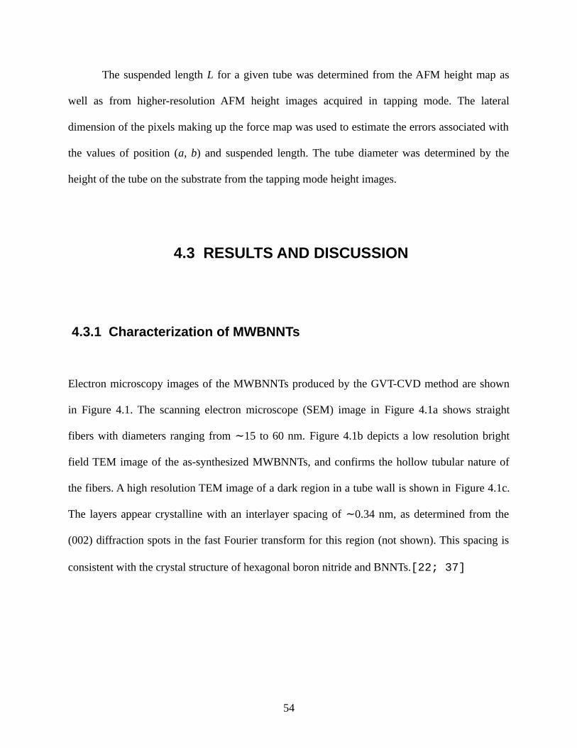
The suspended length L for a given tube was determined from the AFM height map as
well as from higher-resolution AFM height images acquired in tapping mode. The lateral
dimension of the pixels making up the force map was used to estimate the errors associated with
the values of position (a, b) and suspended length. The tube diameter was determined by the
height of the tube on the substrate from the tapping mode height images.
4.3 RESULTS AND DISCUSSION
4.3.1 Characterization of MWBNNTs
Electron microscopy images of the MWBNNTs produced by the GVT-CVD method are shown
in Figure 4.1. The scanning electron microscope (SEM) image in Figure 4.1a shows straight
fibers with diameters ranging from 15 to 60 nm. ∼ Figure 4.1b depicts a low resolution bright
field TEM image of the as-synthesized MWBNNTs, and confirms the hollow tubular nature of
the fibers. A high resolution TEM image of a dark region in a tube wall is shown in Figure 4.1c.
The layers appear crystalline with an interlayer spacing of 0.34 nm, as determined from the∼
(002) diffraction spots in the fast Fourier transform for this region (not shown). This spacing is
consistent with the crystal structure of hexagonal boron nitride and BNNTs.[22; 37]
54
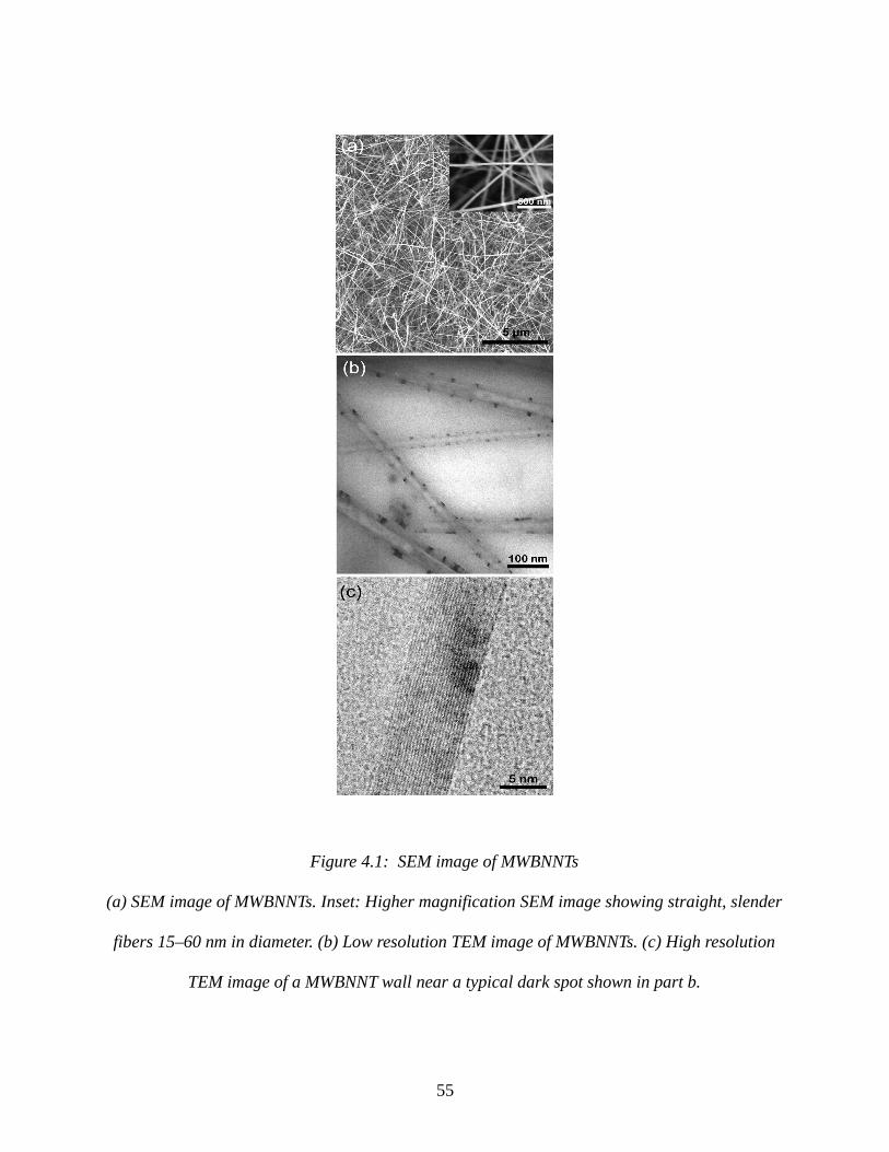
55
Figure 4.1: SEM image of MWBNNTs
(a) SEM image of MWBNNTs. Inset: Higher magnification SEM image showing straight, slender
fibers 15–60 nm in diameter. (b) Low resolution TEM image of MWBNNTs. (c) High resolution
TEM image of a MWBNNT wall near a typical dark spot shown in part b.
The FTIR spectrum of the MWBNNTs is shown in Figure 4.2. For comparison, the
spectrum for commercially available hexagonal BN (h-BN) nanoparticles is also given. The
broadness of the h-BN peaks is likely due to due to both size distribution as well as defects
within the crystal structure, predominantly on the edges of the nanoparticles. The MWBNNT
spectrum exhibits peaks at 1368 and 1510 cm∼ ∼ –1, which correspond to the in-plane transverse
optical (TO) and longitudinal optical (LO) E1u modes of h-BN. The TO E1u mode is a stretching
mode along the tube axis, while the LO E1u mode is a stretching mode along the tube
circumference. A weak feature at around 800 cm–1 is shown enlarged in the inset ofFigure 4.2. A
shoulder is visible at 819 cm∼ –1 and a peak at 806 cm∼ –1. These spectral features correspond to
the out-of-plane TO and LO A2u modes of h-BN. [22; 68]
56
57
Figure 4.2: FTIR spectrum of MWBNNTs
. FTIR spectrum of MWBNNTs (blue line). The FTIR spectrum of h-BN nanoparticles (red line)
is also shown for comparison.
4.3.2 AFM Three-Point Bending
In three-point bending experiments, slender wires can be modeled as an elastic string (pure
stretching), a stiff beam (pure bending), or a combination of the two. Heidelberg et al.[27]
presented a generalized approximation for these behaviors, in which a force F is applied to the
midpoint of the suspended wire and the wire ends are assumed to be clamped:
In the above expression, δ is the deflection of the wire, EB is the bending modulus, A is the cross-
sectional area of the wire, and I is the second moment of area. At small displacements, the wire
undergoes pure bending which is described by the first linear term. At large displacements, axial
tensile stresses are induced as the wire stretches which are described by the cubic second term (F
δ∝ 3). In this study, only pure bending is considered because the experiments are conducted
within the small deflection regime, in which the maximum deflection does not exceed the radius
of the wire.
To model the MWBNNTs in this study as stiff beams undergoing pure bending, Euler–
Bernoulli beam theory was employed. It should be noted that this theory assumes a
homogeneous isotropic material, which is not the case for multiwall nanotubes. Nevertheless,
58
F center=192 EB I
L3 δcenter(1+ A24 I
δcenter2 )
Equation 4.1
simulations indicate that this approximation offers an adequate description of nanotube bending
mechanics prior to buckling.[31] As a result, this approach has been widely used in AFM
bending experiments on nanowires and nanotubes.[38; 45; 52; 54; 59] Unique
solutions to the beam equation depend on the boundary conditions of the beam ends, which can
be considered to be clamped (no deflection or slope at beam end) or simply supported (no
deflection or bending moment at beam end). Beam schematics are presented in Figure 4.3, which
summarize the three models considered in this work: simply supported beam model (a, SSBM),
double clamped beam model (b, DCBM), and mixed support beam model (c, MSBM).[29]
59
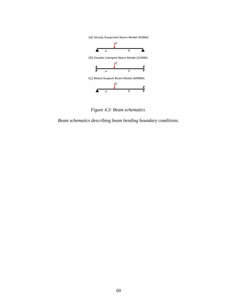
60
Figure 4.3: Beam schematics
Beam schematics describing beam bending boundary conditions.

The corresponding equations are as follows:
SSBM: F =3 L EB I
a2b2 δ
Equation 4.2
DCBM: F =3 L3 EB I
a3b3 δ
Equation 4.3
MSBM: F =12 L3 EB I
a2 b3(3 L+a)
δ
Equation 4.4
In these equations, L is the suspended length of the beam and a and b are the suspended lengths
on both sides of the applied force F, where a + b = L. I, the second moment of area, is taken to be
I = πD4/64 which is defined for a solid cylindrical wire with a circular cross section, where D is
the diameter. Hence, in this approximation of the multiwall nanotube beam, only the outer
diameter is taken into account and not the inner diameter. In order to determine the appropriate
boundary conditions for each tube, the AFM tip is used to apply a force at different positions
61
along the suspended tube, not just at the midpoint. Therefore, AFM force curves (plots of F
versus the tip–sample separation (=beam deflection, δ)) are collected at multiple locations along
the tube. The linear slope of a force curve directly yields the effective tube stiffness, keff= F/δ.
The boundary conditions for the tube are determined by plotting keff versus the position along the
tube (a/L) and performing fits to the various beam models (Equations 4.2-4.4). The bending
modulus EB is then determined using the appropriate beam model.
Figure 4.4 shows SEM (a) and AFM images (b–d) of suspended MWBNNTs on patterned
Si trenches (400 nm wide and 200 nm deep). An AFM height image of a typical MWBNNT
spanning a trench is shown in Figure 4.4b. The height image is subsequently divided up into
pixels (typically 32 × 16 or 64 × 32) by the AFM software, and force curves are collected at each
point (pixel) during the force mapping procedure. The corresponding AFM height map image
illustrating the spatial location (x, y) of each of the force measurements is shown in Figure 4.4c.
The height in each pixel is determined from the Z range distance at which the tip first engages
the sample during the extend portion of the force curve. Figure 4.4d shows the AFM height
image of the MWBNNT after the force map was performed, and its similarity to Figure 4.4b
indicates that the tube did not shift or deform as a result of the force measurements. Typical force
curves collected from different locations on a MWBNNT are shown in Figure 4.5. The red dotted
line corresponds to a force curve obtained from a location where the tube is supported by the Si
substrate (red “x” in Figure 4.4c, illustrative purpose only), while the blue solid line corresponds
to a force curve obtained from a position where the tube is suspended over a trench (blue “x” in
Figure 4.4c, illustrative purpose only). The slope of the blue solid line in Figure 4.5 is equivalent
to keff, as shown
62

63
Figure 4.4: SEM image of MWBNNTs
(a) SEM image of MWBNNTs on patterned Si substrate. (b) AFM height image before force
mapping was performed. (c) Height map image corresponding to a force map acquired at a
deflection trigger of 1 nm. (d) AFM height image after a force map was acquired.

64
Figure 4.5: Force curve
(Red dotted line) Force curve obtained from a point on a tube supported by substrate. (Blue solid
line) Force curve obtained from a point on a tube suspended over a trench.
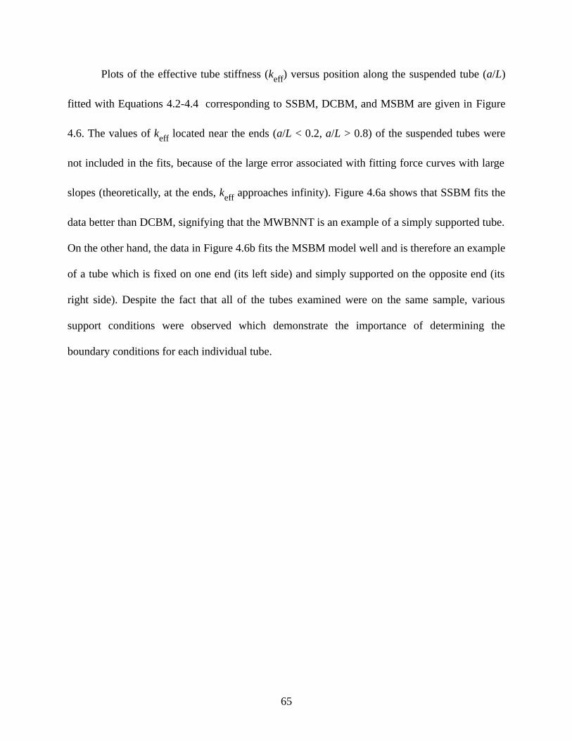
Plots of the effective tube stiffness (keff) versus position along the suspended tube (a/L)
fitted with Equations 4.2-4.4 corresponding to SSBM, DCBM, and MSBM are given in Figure
4.6. The values of keff located near the ends (a/L < 0.2, a/L > 0.8) of the suspended tubes were
not included in the fits, because of the large error associated with fitting force curves with large
slopes (theoretically, at the ends, keff approaches infinity). Figure 4.6a shows that SSBM fits the
data better than DCBM, signifying that the MWBNNT is an example of a simply supported tube.
On the other hand, the data in Figure 4.6b fits the MSBM model well and is therefore an example
of a tube which is fixed on one end (its left side) and simply supported on the opposite end (its
right side). Despite the fact that all of the tubes examined were on the same sample, various
support conditions were observed which demonstrate the importance of determining the
boundary conditions for each individual tube.
65
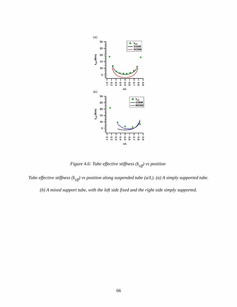
66
Figure 4.6: Tube effective stiffness (keff) vs position
Tube effective stiffness (keff) vs position along suspended tube (a/L). (a) A simply supported tube.
(b) A mixed support tube, with the left side fixed and the right side simply supported.
4.3.3 Elastic Properties
The bending moduli EB determined for 20 tubes with diameters ranging from 18 to 55 nm are
shown in Figure 4.7. EB ranged from 100 ± 20 to 1800 ± 300 GPa, with an average of 760 ± 30
GPa. The error in EB was determined via error propagation, using an error of 10% for the tube
outer diameter D, half the lateral pixel width in the force map for the tube length L and lengths
on each side of the loading position (a, b), and an error of 20% for the effective spring constant
of the tube keff.
It is worth noting that there is the possibility that the calculated bending moduli may be
underestimated due to inaccurate assumptions about the cross-sectional geometry. The nanotubes
were approximated to be solid wires, with a solid circular cross section. This model was chosen
because it was not possible for us to determine the inner diameter of the nanotubes we probed
with AFM, given that we deposited the tubes on a substrate that is not amenable to TEM
analysis. A more accurate model would be a hollow cylinder, with an inner diameter Di and an
outer diameter Do, which results in a second moment of area expression of I = π/64(Do4 – Di
4).
Modeling the tube as a solid wire as opposed to a hollow cylinder underestimates the modulus;
however, in the most extreme case (i.e., very large diameter tube with only a few walls), the
underestimation is on the order of 30%. On the basis of the range of Di/Do ratios observed in
TEM data for 24 tubes in the same MWBNNT production batch as the tubes used in the bending
experiments (presented in the Supporting Information), the underestimation is closer to 10% for
our particular sample.
67

The Young’s modulus of nanotubes and nanowires made of homogeneous isotropic
materials such as B and B4C are typically comparable to the Young’s modulus of the bulk
material.[18; 40; 62] However, for highly anisotropic nanomaterials including CNTs and
BNNTs, the Young’s modulus should theoretically approach an upper limit defined by the in-
plane elastic constant of graphite and h-BN, respectively, which exceeds the Young’s moduli of
the bulk materials by 2 orders of magnitude.[28; 56] For h-BN single crystals, this constant
was measured to be c11 = 811 GPa,[6] while, for single crystal graphite, c11 = 1109 GPa.[28;
56] These measurements correlate well with various theoretical calculations.[24; 46] This
limit is expected to apply to MWBNNTs as well, because the modulus depends mainly on
intrawall bonds. Simulations suggest that the Young’s modulus of a MWCNT is slightly higher
than that of a SWCNT, for the same outer diameter, due to the effect of interwall van der Waals
forces in MWCNTs.[42]
From the plot of EB versus tube outer diameter shown in Figure 4.7, it is evident that
there is a decreasing trend for the bending modulus with increasing tube diameter. The average
EB of the MWBNNTs studied in the present investigation matches the c11 elastic constant of h-
BN quite closely; however, the origin of the wide range of bending moduli and the diameter
dependence requires further analysis.
68

69
Figure 4.7: Bending modulus vs tube outer diameter.
Bending modulus vs tube outer diameter. The beam model used for calculating EB is denoted by
black (SSBM), blue (MSBM), and red (DCBM).
In experimental studies of multiwall nanotubes, a wide range of modulus values has been
measured. For MWCNTs, Treacy et al.[64] were first to show that CNTs have Young’s moduli
in the TPa range, using a thermal excitation method. They found that arc-discharge MWCNTs
with outer diameters ranging from 5.4 to 24.8 nm had Young’s moduli of 0.4 to 4.15 TPa. A
number of other studies have also produced Young’s moduli in the TPa range, for arc-discharge
MWCNTs.[48; 52; 54; 69] Within these studies, despite the focus on the 1 TPa∼
measurements as validation of the superior mechanical properties of CNTs, there are many
instances of tubes with lower moduli, on the order of tens to hundreds of GPa. In the work of
Salvetat et al.,[54] catalytic CVD MWCNTs were also studied and found to have an average
modulus of 27 GPa, which is dramatically lower than the average modulus of 810 GPa measured
for arc-discharge MWCNTs. Additional studies also observe lower moduli for catalytic CVD and
pyrolytic MWCNTs, in certain cases as low as tens of GPa.[19; 21; 43] Typically,
catalytic CVD and pyrolysis synthesis methods produce tubes with defective structures
compared with the highly crystalline tubes synthesized by arc-discharge. While point defects do
not affect the modulus by more than a few percent,[55] extended defects can cause the modulus
to drop by as much as 2 orders of magnitude.[21; 54]
In some studies, within sample sets of nanotubes produced under the same conditions, the
modulus is observed to drop with increasing tube diameter. This diameter dependence can be
attributed to three possibilities, namely, the probing of an elastic rippling mode in bending
experiments,[48] the presence of defects,[38; 43] or shear effects. Because of the highly
anisotropic nature of the BNNTs, we do not consider surface stress effects which are known to
give rise to diameter dependent moduli in relatively isotropic nanowires and nanotubes.[16]
Due to the linearity of the force curves obtained in the present study, it is unlikely that rippling
70
modes are the cause of the low moduli measurements observed for larger tubes. Although it was
not rare to acquire force curves which exhibited kinks, potentially due to tube buckling or tip
slipping events, fits were only made to the initial linear portion of the force curves (for
deflections less than 10 nm) after contact. In terms of defects, the low resolution TEM image
(Figure 4.1b) shows long, straight nanotubes with uniform diameters. The high resolution TEM
image (Figure 4.1c) shows that the dark spots present in the tube walls in Figure 4.1b are
crystalline. The MWBNNTs do not appear to exhibit the type of pronounced structural defects
that were found to affect the modulus of catalytic or pyrolytic MWCNTs, as discussed above. In
beam bending experiments, shear must always be considered for short, stocky beams—those
which have a length-to-diameter ratio of L/D < 10. The length-to-diameter ratio L/D was
measured to be greater than 10 for all tubes in this study, which indicates that, if shear effects are
present, they are not a result of the experimental geometry. Rather, they can be an indication of a
material’s anisotropy.[33; 38]
If shear effects are present, then the bending modulus is not equivalent to the Young’s
modulus. In order to determine whether the Young’s modulus of the MWBNNTs is diameter
dependent, the contribution of shear deflection to the total deflection in the bending experiment
must be quantified. This approach follows Salvetat and co-workers’ bending and shear analysis
of single-wall CNT ropes.[53]
The bending modulus is related to the Young’s modulus EY and the shear modulus G
using the following relationship, determined by Timoshenko beam theory:[34; 38; 53;
63]
71

1EB
=1E y
+γf s
G ( D2
L2 )
Equation 4.5
In this expression, fs is a shape factor which has a value of 10/9 for a cylindrical beam and γ is a
shear term coefficient with values of 3, 1.715, and 0.75 for DCBM, MSBM, and SSBM,
respectively. The Timoshenko beam theory converges to the Euler–Bernoulli beam theory when
the beam is rigid in shear (G → ∞). In this case, the bending modulus is equal to the Young
modulus and is not diameter dependent (which is not the case here). EY and G in our case can be
estimated by plotting 1/EB against (D2/L2), as shown in Figure 4.8. A linear fit weight by the error
in 1/EB was obatined for a trimmed sata set of 16 tubes. The shear coefficient was taken as γ =
1.152, determined by the number of tubes exhibiting each type of boundary condition (16 tubes
total = 12 simply supported tubes + 2 mixed support tubes + 2 doubly clamped tubes). EY and G
were determined to be 1800 ± 300 and 7 ± 1 GPa, respectively. The expected shear modulus for a
MWBNNT should be on the order of several hundred GPa, based on the calculations for
MWCNTs[42; 58] which find that GMWCNT 500 GPa. This value is on the order of the∼
intralayer shear modulus. However, the value of G that we determined for MWBNNTs is much
lower than this, and is close to the value of the c44 elastic constant of h-BN, c44 = 7.7 ± 5,
measured by Bosak et al.[6] This elastic constant is equivalent to the interlayer shear modulus
72

of h-BN, and describes the shear between basal planes. In the case of the MWBNNT structure,
this corresponds to shearing between tube walls, which can only occur if there are discontinuities
due to the presence of extended defects within the tube walls.e
73

74
Figure 4.8: Determination of the Young’s modulus and shear modulus
Determination of the Young’s modulus and shear modulus via a fit to a plot of 1/EB vs (D/L)2.
The beam model used for calculating 1/EB is denoted by black (SSBM), blue (MSBM), and red
(DCBM). The equation used for the fit is 1/EB= 1/EY+ 1.139fs/G (D2/L2).

Although no extensive defects are apparent from the TEM characterization of the
MWBNNTs, as discussed above, the dark spots within the tube walls in the low resolution TEM
image (Figure 4.1b) and their somewhat regular pattern within a given tube warrant additional
consideration. A detailed electron diffraction study by Celik-Aktas et al.[7] determined that the
dark spots can be attributed to a helical nanotube structure in which the tube is comprised of two
or more helices (each comprised of multiple walls) which wrap to form the entire nanotube. In
this structure, the dark spots correspond to a strongly diffracting helix, which is locally highly
crystalline. The highly crystalline regions are joined together by line defects which result in a
faceted helix. The lighter regions of the tube wall form the other helix, which possesses the
conventional nested coaxial cylindrical structure expected for multiwall nanotubes. On the basis
of this multihelix nanotube structure, it is conceivable that the line defects within the faceted
helix as well as the interface between faceted and cylindrical helices make interwall shearing a
possibility. Therefore, as our analysis of the bending data suggests, shear cannot be ignored in
the calculation of the elastic modulus, and shear effects arise from nanotube anisotropy (G ≪
EY) and the presence of defects within the nanotubes, and not from the experimental geometry.
Our finding that the shear modulus of MWBNNTs is orders of magnitude smaller than
the Young’s modulus indicates that the existing theoretical models are not sufficient in predicting
the mechanical properties of such extremely anisotropic structures, particularly when structural
defects are present.[42] Experiments performed on MWCNTs support this assertion. Guhados
et al.[25] determined that EY = 350 ± 110 GPa and G = 1.4 ± 0.3 GPa for 13 MWCNTs grown
by a CVD method, while Wei et al.[66] found that EY ranged from 300 to 900 GPa while G
ranged from 30 to 800 MPa, for a sample of eight tubes. Both studies attribute the low shear
modulus to defects in the structure of the nanotubes. There are several possible benefits of
75
having a low shear modulus: (1) Taking advantage of its high melting temperature, the shear
modulus of MWBNNTs cast within metals or ceramics would enable damping of vibrations. This
could result in quieter, more durable materials.[2; 17; 60] (2) Local distortions allowed due
to the low shear modulus could enable MWBNNTs to adapt to local structure variations while
maintaining rigidity on long length scales (longitudinal distortions), imparting toughness to
otherwise brittle composite materials.[69] (3) The mutual compensation of shear modulus and
Young’s modulus, whereby tubes of different diameters have similar bending stiffness, could
allow for lower purity BNNT materials in BNNT coated interfaces for release applications.[26;
41] (4) With a shear modulus on the order of the value for h-BN, MWBNNTs can be used as a
high-temperature solid lubricant additive in industrially relevant composites. [8] The
nanotube structures would have the added advantages of enabling more efficient heat transport
on longitudinal length scales,[4] and increasing the wear resistance of the composite due to
reinforcement of the matrix.[71]
4.4 CONCLUSIONS
The bending modulus of individual multiwall boron nitride nanotubes (MWBNNTs) was
measured via AFM bending experiments. Boundary conditions for the beam bending model were
determined by using a force mapping technique. MWBNNTs were found to have excellent
mechanical properties, with an average bending modulus of 760 ± 30 GPa, which is consistent
with the theoretically predicted value for BNNTs. Shear effects were found to be non-negligible,
and the Young’s modulus and shear modulus were determined to be 1800 ± 300 and 7 ± 1 GPa,
76

respectively. The experimental geometry and the dimensions of the nanotubes were not major
contributors to the shear effects; rather, it is likely that interwall shearing occurred between
crystalline and faceted cylindrical helices in these MWBNNTs.
77

4.5 BIBLIOGRAPHY
[1] Arenal, R.; Golberg, D.; Wang, M.-S.; Xu, Z. and Loiseau, A. (2011). , Nanotechnology 22 : 265704.
[2] Balani, K. and Agarwal, A. (2008). , J. Appl. Phys. 104 : 063517.
[3] Bando, Y.; Golberg, D.; Tang, C.; Terao, T. and Zhi, C. Y. (2010). , Pure Appl. Chem. 82 : 2175.
[4] Bando, Y.; Golberg, D.; Tang, C.; Zhang, J.; Ding, X.; Fan, S. and Liu, C. (2006). , J. Phys. Chem. B 110 : 10354.
[5] Blase, X. (1994). , Europhys. Lett. 28 : 335.
[6] Bosak, A.; Serrano, J.; Krisch, M.; Watanabe, K.; Taniguchi, T. and Kanda, H. (2006). , Phys. Rev. B 73 : 041402.
[7] Celik-Aktas, A.; Zuo, J. M.; Stubbins, J. F.; Tang, C. C. and Bando, Y. (2005). , Acta Crystallogr., Sect. A 61 : 533.
[8] Chen, W.; Gao, Y.; Chen, C. and Xing, J. (2010). , Wear 269 : 241.
[9] Chen, Y.; Dorgan, B. L.; McIlroy, D. N. and Aston, D. E. (2006). , J. Appl. Phys. 100 : 104301.
[10] Chen, Y.; Zou, J.; Campbell, S. J. and Caer, G. L. (2004). , Appl. Phys. Lett. 84 : 2430.
[11] Choi, S. R.; Bansal, N. P. and Garg, A. (2007). , Mater. Sci. Eng., A 460-461 : 509.
[12] Chopra, N. G.; Luyken, R. J.; Cherrey, K.; Crespi, V. H.; Cohen, M. L.; Louie, S. G. and Zettl, A. (1995). , Science 269 : 966.
[13] Chopra, N. G. and Zettl, A. (1998). , Solid State Commun. 105 : 297.
[14] Chowdhury, R. and Adhikari, S. (2011). , IEEE Trans. Nanotechnol. 10 : 659.
[15] Ciofani, G.; Raffa, V.; Yu, J.; Chen, Y.; Obata, Y.; Takeoka, S.; Menciassi, A. and Cuschieri, A. (2009). , Curr. Nanosci. 5 : 33.
[16] Cuenot, S.; Frétigny, C.; Demoustier-Champagne, S. and Nysten, B. (2004). , Phys. Rev. B 69 : 165410.
78

[17] Deng, C. F.; Wang, D. Z.; Zhang, X. X. and Ma, Y. X. (2007). , Mater. Lett. 61 : 3229.
[18] Ding, W.; Calabri, L.; Chen, X.; Kohlhaas, K. M. and Ruoff, R. S. (2006). , Compos. Sci. Technol. 66 : 1112.
[19] Gaillard, J.; Skove, M. and Rao, A. M. (2005). , Appl. Phys. Lett. 86 : 233109.
[20] Gangadean, D.; David, N. M.; Brian, E. F. and Aston, D. E. (2010). , Nanotechnology 21 : 225704.
[21] Gao, R. P.; Wang, Z. L.; Bai, Z. G.; de Heer, W. A.; Dai, L. M. and Gao, M. (2000). , Phys. Rev. Lett. 85 : 622.
[22] Ghassemi, H. M.; Lee, C. H.; Yap, Y. K. and Yassar, R. S. (2010). , J. Appl. Phys. 108 : 024314.
[23] Golberg, D.; Costa, P. M. F. J.; Lourie, O.; Mitome, M.; Bai, X.; Kurashima, K.; Zhi, C.; Tang, C. and Bando, Y. (2007). , Nano Lett. 7 : 2146.
[24] Green, J. F.; Bolland, T. K. and Bolland, J. W. (1976). , J. Chem. Phys. 64 : 656.
[25] Guhados, G.; Wan, W.; Sun, X. and Hutter, J. L. (2007). , J. Appl. Phys. 101 : 033514.
[26] Haubner, R.; Wilhelm, M.; Weissenbacher, R.; Lux, B. and Jansen, M., 2002. High Performance Non-Oxide Ceramics II. , .
[27] Heidelberg, A.; Ngo, L. T.; Wu, B.; Phillips, M. A.; Sharma, S.; Kamins, T. I.; Sader, J. E. and Boland, J. J. (2006). , Nano Lett. 6 : 1101.
[28] Hernandez, E.; Goze, C.; Bernier, P. and Rubio, A. (1999). , Appl. Phys. A: Mater. Sci. Process. 68 : 287.
[29] Hsu, T. H., 1988. Structural Engineering and Applied Mechanics Data Handbook. , .
[30] Hutter, J. L. and Bechhoefer, J. (1993). , Rev. Sci. Instrum. 64 : 1868.
[31] Iijima, S.; Brabec, C.; Maiti, A. and Bernholc, J. (1996). , J. Chem. Phys. 104 : 2089.
[32] Jaffrennou, P.; Barjon, J.; Lauret, J. S.; Maguer, A.; Golberg, D.; Attal-Tretout, B.; Ducastelle, F. and Loiseau, A. (2007). , Phys. Status Solidi B 244 : 4147.
[33] Kaplan-Ashiri, I.; Cohen, S. R.; Apter, N.; Wang, Y.; Seifert, G.; Wagner, H. D. and Tenne, R. (2007). , J. Phys. Chem. C 111 : 8432.
[34] Kis, A.; Mihailovic, D.; Remskar, M.; Mrzel, A.; Jesih, A.; Piwonski, I.; Kulik, A. J.; Benoit, W. and Forro, L. (2003). , Adv. Mater. 15 : 733.
[35] Kluge, D.; Abraham, F.; Schmidt, S.; Schmidt, H.-W. and Fery, A. (2010). , Langmuir 26 : 3020.
79

[36] Lahiri, D.; Singh, V.; Benaduce, A. P.; Seal, S.; Kos, L. and Agarwal, A. (2011). , J. Mech. Behav. Biomed. Mater. 4 : 44.
[37] Lee, C. H.; Wang, J. S.; Kayatsha, V. K.; Huang, J. Y. and Yap, Y. K. (2008). , Nanotechnology 19 : 455605.
[38] Lee, K.; Lukić, B.; Magrez, A.; Seo, J. W.; Briggs, G. A. D.; Kulik, A. J. and Forró, L. (2007). , Nano Lett. 7 : 1598.
[39] Li, L. H.; Chen, Y.; Lin, M. Y.; Glushenkov, A. M.; Cheng, B. M. and Yu, J. (2010). , Appl. Phys. Lett. 97 : 141104.
[40] Lin, C.-H.; Ni, H.; Wang, X.; Chang, M.; Chao, Y. J.; Deka, J. R. and Li, X. (2010). , Small 6 : 927.
[41] Lipp, A.; Schwetz, K. A. and Hunold, K. (1989). , J. Eur. Ceram. Soc. 5 : 3.
[42] Lu, J. P. (1997). , Phys. Rev. Lett. 79 : 1297.
[43] Lukic, B.; Forro, L.; Seo, J. W.; Bacsa, R. R.; Delpeux, S.; Beguin, F.; Bister, G.; Fonseca, A.; Nagy, J. B. and Kis, A. (2005). , Nano Lett. 5 : 2074.
[44] Ma, R. Z.; Bando, Y.; Zhu, H. W.; Sato, T.; Xu, C. L. and Wu, D. H. (2002). , J. Am. Chem. Soc. 124 : 7672.
[45] Ni, H.; Li, X. D. and Gao, H. S. (2006). , Appl. Phys. Lett. 88 : 043108.
[46] Ohba, N.; Miwa, K.; Nagasako, N. and Fukumoto, A. (2001). , Phys. Rev. B 63 : 115207.
[47] Pampaloni, F. and Florin, E.-L. (2008). , Trends Biotechnol. 26 : 302.
[48] Poncharal, P.; Wang, Z. L.; Ugarte, D. and de Heer, W. A. (1999). , Science 283 : 1513.
[49] Ravichandran, J.; Manoj, A. G.; Liu, J.; Manna, I. and Carroll, D. L. (2008). , Nanotechnology 19 : 085712.
[50] Reddy, A. L. M.; Tanur, A. E. and Walker, G. C. (2010). , Int. J. Hydrogen Energy 35 : 4138.
[51] Rubio, A.; Corkill, J. L. and Cohen, M. L. (1994). , Phys. Rev. B 49 : 5081.
[52] Salvetat, J. P.; Bonard, J. M.; Thomson, N. H.; Kulik, A. J.; Forro, L.; Benoit, W. and Zuppiroli, L. (1999). , Appl. Phys. A: Mater. Sci. Process. 69 : 255.
[53] Salvetat, J. P.; Briggs, G. A. D.; Bonard, J. M.; Bacsa, R. R.; Kulik, A. J.; Stockli, T.; Burnham, N. A. and Forro, L. (1999). , Phys. Rev. Lett. 82 : 944.
[54] Salvetat, J. P.; Kulik, A. J.; Bonard, J. M.; Briggs, G. A. D.; Stockli, T.; Metenier, K.; Bonnamy, S.; Beguin, F.; Burnham, N. A. and Forro, L. (1999). , Adv. Mater. 11 : 161.
80

[55] Sammalkorpi, M.; Krasheninnikov, A.; Kuronen, A.; Nordlund, K. and Kaski, K. (2004). , Phys. Rev. B 70 : 245416.
[56] Santosh, M.; Maiti, P. K. and Sood, A. K. (2009). , J. Nanosci. Nanotechnol. 9 : 5425.
[57] Shanmugham, S.; Jeong, J.; Alkhateeb, A. and Aston, D. E. (2005). , Langmuir 21 : 10214.
[58] Shen, L. and Li, J. (2005). , Phys. Rev. B 71 : 035412.
[59] Shin, M. K.; Kim, S. I.; Kim, S. J.; Kim, S. K.; Lee, H. and Spinks, G. M. (2006). , Appl. Phys. Lett. 89 : 231929.
[60] Sueyoshi, H.; Rochman, N. T. and Kawano, S. (2003). , J. Alloys Compd. 355 : 120.
[61] Suryavanshi, A. P.; Yu, M. F.; Wen, J. G.; Tang, C. C. and Bando, Y. (2004). , Appl. Phys. Lett. 84 : 2527.
[62] Tao, X.; Dong, L.; Wang, X.; Zhang, W.; Nelson, B. J. and Li, X. (2010). , Adv. Mater. 22 : 2055.
[63] Timoshenko, S., 1955. Strength of materials. , .
[64] Treacy, M. M. J.; Ebbesen, T. W. and Gibson, J. M. (1996). , Nature 381 : 678.
[65] Verma, V.; Jindal, V. K. and Dharamvir, K. (2007). , Nanotechnology 18 : 435711.
[66] Wei, X.-L.; Liu, Y.; Chen, Q.; Wang, M.-S. and Peng, L.-M. (2008). , Adv. Funct. Mater. 18 : 1555.
[67] Wen, B. M.; Sader, J. E. and Boland, J. J. (2008). , Phys. Rev. Lett. 101 : 175502.
[68] Wirtz, L. and Rubio, A. (2003). , IEEE Trans. Nanotechnol. 2 : 341.
[69] Wong, E. W.; Sheehan, P. E. and Lieber, C. M. (1997). , Science 277 : 1971.
[70] Zhi, C. Y.; Bando, Y.; Wang, W. L. L.; Tang, C. C. C.; Kuwahara, H. and Golberg, D. (2008). , J. Nanomater. : 642036.
[71] Zhou, S.-m.; Zhang, X.-b.; Ding, Z.-p.; Min, C.-y.; Xu, G.-l. and Zhu, W.-m. (2007). , Composites, Part A 38 : 301.
81

5.0 PHOTONIC CRYSTALS INTRODUCTION
Advances in imaging, communication, sensing and other applications have been driven over the
past fifty years through advances in laser technology, non-linear optics and imaging optics.
However, advances in nanoscale optics and nanophotonics have yet to have their full impact on
society. The foundational science underling nanophotonics in particular, plasmonics and photonic
crystals, has been laid in the past few decades. [3; 5; 6]
Photonic crystals, which are discussed in this section, are commonly defined as a class of
materials which possess significantly strong periodic modulation of refractive index on the order
of the optical wavelength, typically 100 to 1000 nm. These materials exhibit wavelength
selective light reflection and other diffraction related phenomena arising from a photonic band
gap. A photon band gap is the range of photon energies for which light cannot propagate in a
material. Photonic crystals have been designed with photonic band gaps that prohibit photon
propagation in one or more wavelength bands.
The origin of a photonic crystal’s properties can be understood by consideration of the
light wave’s interference in the material. In analogy to the interference of electron waves and
electron band gap theory explaining many of the electrical properties of semiconductors,
periodicity is responsibly for the photonic band gap effect. Below I explain how this effect arises
for a one-dimensional photonic bandgap. The two and three dimensional photonic band gap
82

materials, which are described in Chapters 6 and 7, can be understood by extending the one-
dimensional Bragg refraction framework to include Bragg diffraction of waves propagating in
any direction.
83
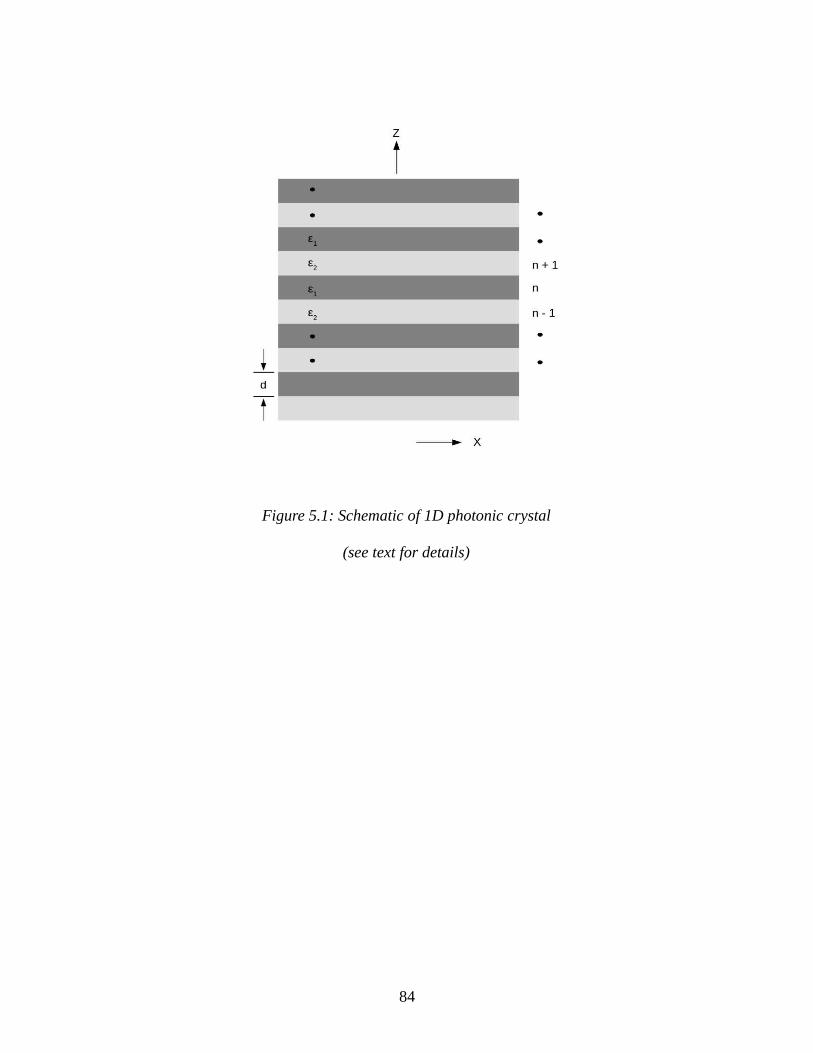
84
Figure 5.1: Schematic of 1D photonic crystal
(see text for details)
5.1 THE PHOTONIC BAND GAP
Consider a system composed of an infinite number of planar layers of thickness d; assume that
the layers are oriented perpendicular to the z direction, and that the dielectric constant of the
layers alternates between the values ε1 and ε2, ( see Figure 5.1). The optical wavevector inside
the material is given by k = (kx, ky, kz). In addition, consider the system non-magnetic, μ1 = μ2 =
1 and, lossless. In this approximation, two classes of electronic field modes can be defined, TE
modes, where the electric field vector is parallel to the layer boundaries, and TM modes, where
the magnetic field vector is parallel to the layer boundaries. Using the typical separation of
variables method allows the TE and TM modes to be expressed by,
TE : E(r ) = E(z )ei (k x x+k y y)nx
Equation 5.1
TM : H (r ) = H (z)e i(kx x+ ky y )nx
Equation 5.2
85
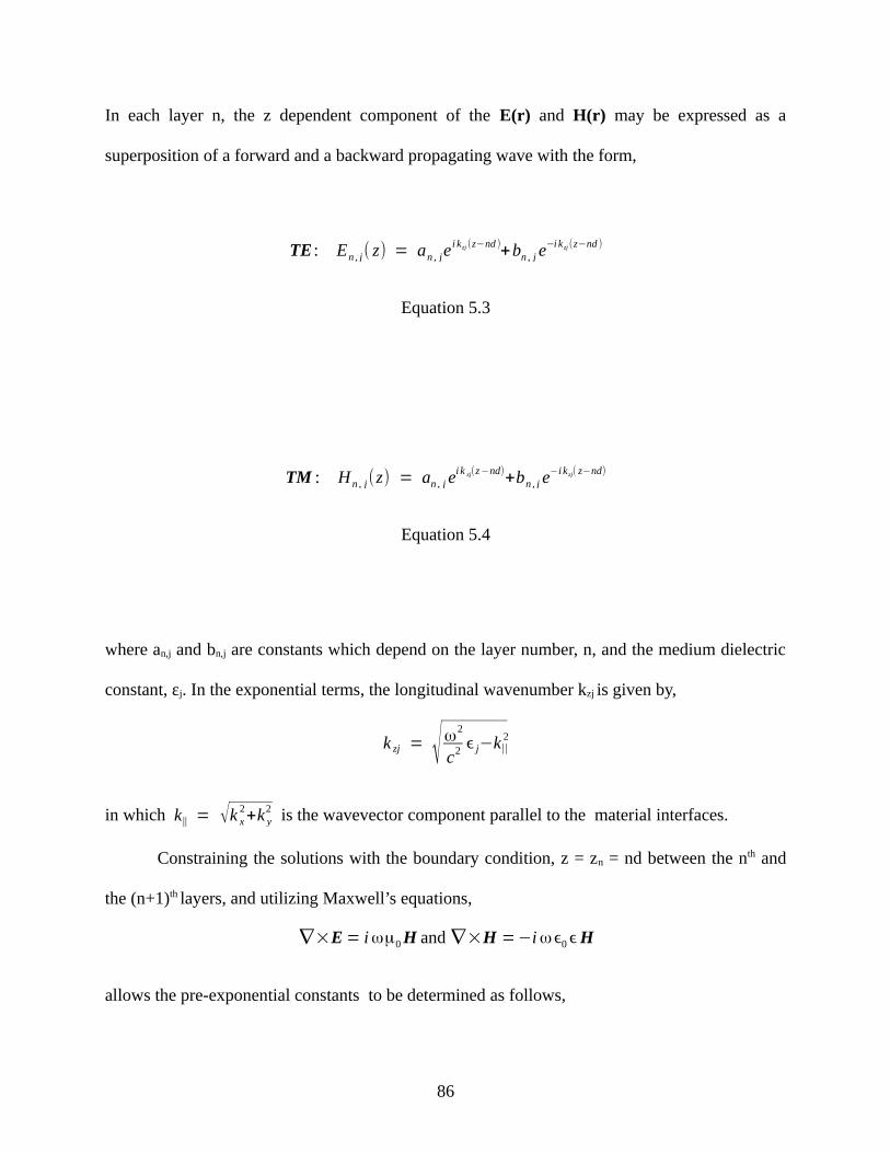
In each layer n, the z dependent component of the E(r) and H(r) may be expressed as a
superposition of a forward and a backward propagating wave with the form,
TE : En , j( z) = an , jei k zj (z−nd )
+bn , j e−i k zj (z−nd )
Equation 5.3
TM : H n , j(z) = an , j ei k zj(z−nd)
+bn , j e−i k zj( z−nd)
Equation 5.4
where an,j and bn,j are constants which depend on the layer number, n, and the medium dielectric
constant, εj. In the exponential terms, the longitudinal wavenumber kzj is given by,
k zj = √ω2
c2 ϵ j−k||2
in which k|| = √k x2+k y
2 is the wavevector component parallel to the material interfaces.
Constraining the solutions with the boundary condition, z = zn = nd between the nth and
the (n+1)th layers, and utilizing Maxwell’s equations,
∇×E= iωμ0 H and ∇×H =−iωϵ0ϵH
allows the pre-exponential constants to be determined as follows,
86
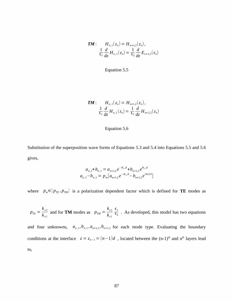
TM : H n ,1(zn)= H n+1,2(zn) ,1ϵ1
ddz
H n , 1(zn)=1ϵ2
ddz
En+1,2(zn)
Equation 5.5
TM : Hn , 1( zn)= Hn+1,2(zn) ,1ϵ1
ddz
H n, 1(zn)=1ϵ2
ddz
Hn+1,2(zn)
Equation 5.6
Substitution of the superposition wave forms of Equations 5.3 and 5.4 into Equations 5.5 and 5.6
gives,
an ,1+bn , 1= an+1,2 e−ikz 2d+bn+1,2 eik z 2 d
an , 1−bn ,1= pm[an+1,2 e−ik z2 d−bn+1,2 e i kz2d
]
where pm∈pTE , pTM is a polarization dependent factor which is defined for TE modes as
pTE =k z2
k z1and for TM modes as pTM =
kz2
kz1
ϵ1ϵ2
. As developed, this model has two equations
and four unknowns, an , 1, bn,1 , an+1,2 , bn+1,2 for each mode type. Evaluating the boundary
conditions at the interface z = zn−1= (n−1)d , located between the (n-1)th and nth layers lead
to,
87
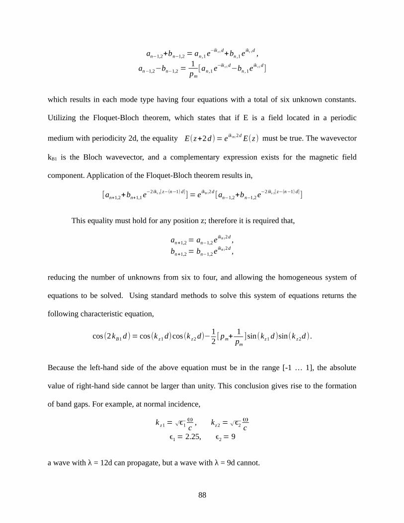
an−1,2+bn−1,2 = an ,1 e−ik z 1 d+bn ,1 e ikz 1d ,
an−1,2−bn−1,2 =1pm
[an ,1 e−ik z 1 d−bn , 1e ik z1 d
]
which results in each mode type having four equations with a total of six unknown constants.
Utilizing the Floquet-Bloch theorem, which states that if E is a field located in a periodic
medium with periodicity 2d, the equality E(z+2d )= e ik B1 2d E(z ) must be true. The wavevector
kB1 is the Bloch wavevector, and a complementary expression exists for the magnetic field
component. Application of the Floquet-Bloch theorem results in,
[an+1,2+bn+1,1 e−2 ikz 2[ z−(n−1) d]] = e ikB 12d
[an−1,2+bn−1,2 e−2 ikz 2[ z−(n−1) d]]
This equality must hold for any position z; therefore it is required that,
an+1,2= an−1,2 e ikB 12d ,
bn+1,2= bn−1,2 e ikB 12d ,
reducing the number of unknowns from six to four, and allowing the homogeneous system of
equations to be solved. Using standard methods to solve this system of equations returns the
following characteristic equation,
cos (2kB1 d )= cos (k z1 d)cos (k z2 d)−12[ pm+
1pm
]sin(kz1 d )sin(k z2d ) .
Because the left-hand side of the above equation must be in the range [-1 … 1], the absolute
value of right-hand side cannot be larger than unity. This conclusion gives rise to the formation
of band gaps. For example, at normal incidence,
k z 1= √ϵ1ωc
, kz 2 = √ϵ2ωc
ϵ1= 2.25, ϵ2= 9
a wave with λ = 12d can propagate, but a wave with λ = 9d cannot.
88
5.2 DEFECTS AND DISORDER IN PHOTONIC CRYSTALS
When defects or disorder interrupt the dielectric periodicity of photonic crystals the photonic
band gap can be affected, and even destroyed. Photons with energies within the photonic band
gap cannot propagate through photonic crystals. Research efforts have been conducted on
photonic crystal waveguide structures created by the introduction of line defects into a two
dimensional photonic crystal.[1; 2; 4; 6] When a line of defects are introduced, photons with
frequencies within the band gap can propagate through the crystal using the line defect as a
waveguide. This approach has been used to create waveguide structures capable of guiding light
around sharp bends via narrow channels with minimal losses. Photonic crystal-based
waveguides provide a basis for the construction of photonic circuitry components. Tactical
introduction of defects in photonic crystals can be used to localize or guide light; i.e., selective
destruction of photonic crystal order is often desirable. Thus understanding and quantifying
defects and disorder in a photonic band gap material is important.
Disorder in photonic crystals degrades the magnitude and increases the width of Bragg
diffraction peaks. Fabrication of photonic crystals with well-defined band gaps requires highly
ordered and long-range crystal structures. The optical properties of photonic crystals are most
often characterized using UV-Vis spectroscopy and refractometry. Angle-resolved, UV-Vis
measurements of photonic crystals enable comparison to theoretically predicted Bragg
diffraction. Electron microscopies are typically used to assess crystal morphology and allow
quantification of crystal ordering.
89
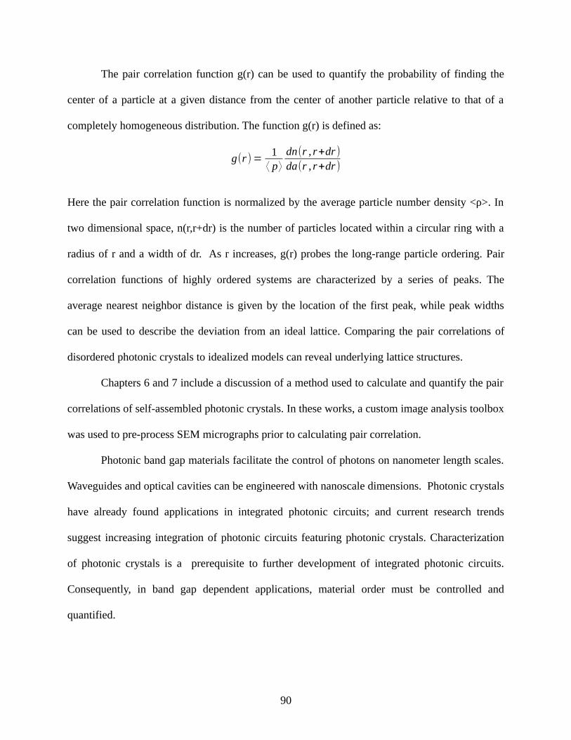
The pair correlation function g(r) can be used to quantify the probability of finding the
center of a particle at a given distance from the center of another particle relative to that of a
completely homogeneous distribution. The function g(r) is defined as:
g(r )=1⟨ p⟩
dn(r , r+dr )da(r , r+dr )
Here the pair correlation function is normalized by the average particle number density <ρ>. In
two dimensional space, n(r,r+dr) is the number of particles located within a circular ring with a
radius of r and a width of dr. As r increases, g(r) probes the long-range particle ordering. Pair
correlation functions of highly ordered systems are characterized by a series of peaks. The
average nearest neighbor distance is given by the location of the first peak, while peak widths
can be used to describe the deviation from an ideal lattice. Comparing the pair correlations of
disordered photonic crystals to idealized models can reveal underlying lattice structures.
Chapters 6 and 7 include a discussion of a method used to calculate and quantify the pair
correlations of self-assembled photonic crystals. In these works, a custom image analysis toolbox
was used to pre-process SEM micrographs prior to calculating pair correlation.
Photonic band gap materials facilitate the control of photons on nanometer length scales.
Waveguides and optical cavities can be engineered with nanoscale dimensions. Photonic crystals
have already found applications in integrated photonic circuits; and current research trends
suggest increasing integration of photonic circuits featuring photonic crystals. Characterization
of photonic crystals is a prerequisite to further development of integrated photonic circuits.
Consequently, in band gap dependent applications, material order must be controlled and
quantified.
90
5.3 BIBLIOGRAPHY
[1] Baba, T.; Fukaya, N. and Yonekura, J. (1999). Observation of light propagation in photonic crystal optical waveguides with bends, ELECTRONICS LETTERS-IEE 35 : 654-654.
[2] Busch, K.; Lölkes, S.; Wehrspohn, R. B. and Föll, H. (2004). Photonic crystals, New York: Willey : 241-247.
[3] Di Bartolo, B.; Collins, J. and Silvestri, L., 2013. Nano-optics for enhancing light-matter interactions on a molecular scale: plasmonics, photonic materials and sub-wavelength resolution. Springer, Dordrecht.
[4] Joannopoulos, J. D.; Johnson, S. G.; Winn, J. N. and Meade, R. D., 2011. Photonic crystals: molding the flow of light. Princeton university press, .
[5] Novotny, L. and Hecht, B., 2012. Principles of nano-optics. Cambridge University Press, Cambridge, UK;New York;.
[6] Soukoulis, C. M., 2012. Photonic crystals and light localization in the 21st century. Springer Science & Business Media, .
91
6.0 CHARGE STABILIZED CRYSTALLINE COLLOIDAL
ARRAYS AS TEMPLATES FOR FABRICATION OF
NON-CLOSE-PACKED INVERTED PHOTONIC
CRYSTALS
Author list: Justin J. Bohn, Matti Ben-Moshe, Alexander Tikhonov, Dan Qu, Daniel N. Lamont,
and Sanford A. Asher
Author contribution: The author of this dissertation was responsible for characterizing the
degree of order of the photonic crystals, providing interpretation of the results and contributing
to the preparation of the manuscript. This work has been publish as Journal of Colloid and
Interface Science 2010, 344, 298
6.1 INTRODUCTION
The last two decades has seen the emergence of the important field of photonic crystals. The
name photonic crystals was coined to describe materials which control light propagation through
periodic variations in their optical dielectric constants.[29; 31; 72]
92
Photonic crystal materials are of major technological significance in areas such as optical
computing and communications where photonic devices are being developed to replace
electronic devices.[3; 27; 29; 30; 40; 49; 61] Photonic crystal materials also offer
the possibility to fabricate complete 3-D photonic bandgap materials which exclude
electromagnetic radiation (including the vacuum field) within its finite spectral bandgap.[10;
48] Phenomena such as spontaneous emission are suppressed in these materials.[47; 72]
Lithography is the most straightforward method to fabricate two and three dimensional
photonic crystal materials for photonic applications.[1; 14-17; 26; 38; 50; 60] This
top down fabrication methodology is highly successful in fabricating complex photonic crystal
materials. These fabricated structures are extremely useful in demonstrating proof of concept for
photonic crystal devices. However, lithographic processes are expensive, and this cost is likely to
prevent commercialization of many photonic crystal devices.
Thus, much of the recent work in photonic crystal fabrication has utilized colloidal
particle self assembly. The utility of colloidal particle self assembly is evident from the photonic
crystal materials found in nature. For example, earth mined opals are photonic crystals formed
from the close packed self assembly of silica colloidal particles.[56] The first work fabricating
artificial opals used gravity sedimentation to obtain photonic crystal periodic structures.[19;
44; 63]
Much of the recent colloidal particle self assembly work has emphasized methods that
form close packed photonic crystal materials. These methods utilize variances of vertical
colloidal particle deposition methods.[28; 36; 64; 67; 73] Surprisingly, many of these
close packed assembly methods claim formation of fcc crystals[25; 37; 59; 63] which
require that the self assembly select for the fcc crystal form, rather than the random stacked
93

crystal forms, which would normally result from simple hard sphere interparticle interactions;
the fcc crystal assembly process requires long range interparticle interactions that select for fcc
ABCABC layer packing.
A major limitation of close packed photonic crystal systems is that their ordering, and
therefore their photonic crystal properties depend upon the colloidal particle size polydispersity.
Clearly, increasing size polydispersity will degrade ordering.[55] Further, charge
polydispersity will degrade ordering to the extent that electrostatic interactions are involved in
the close packing mechanism. Disorder in the photonic crystals degrade the magnitude and
increase the widths of the Bragg diffraction peaks.[39; 55; 62]
Fabrication of a complete 3-D photonic bandgap material requires specific crystal
structures and a very large periodic variation in its optical dielectric constant. The most
straightforward approach to forming a complete 3-D photonic bandgap crystal would utilize an
inverse opal fcc crystal structure that requires a minimum refractive index ratio of 2.8.[12] The
inverse opal structure is formed within an fcc photonic crystal by infiltrating an fcc photonic
crystal structure with a high refractive index material, and then removing the original fcc
spheres, leaving an inverse fcc lattice of air holes with a refractive index of n=1.
Optimization of the inverse opal crystal structure would permit decreasing the required
refractive index modulation. For example, it was recently found that an inverted non close
packed fcc lattice shows a wider photonic band gap (10 %) than does a close packed inverted fcc
crystal structure with the same lattice constant.[20; 23]
94
The recent work which has attempted to generate non close packed photonic crystals has
utilized thermal sintering and etching of close packed colloidal crystals.[21; 42; 43] This
work has also employed conformally backfilling[23; 35; 45] these close packed colloidal
crystals. It should be noted that the resulting photonic crystal materials retain the disorder present
in the original close packed crystals.
In the work here we demonstrate a straightforward method to form non close-packed
highly ordered fcc direct and inverse opal silica photonic crystals materials. We show that size
and charge polydispersity has surprisingly little impact on ordering for colloidal particle systems
that are formed through electrostatic self assembly. Our group has utilized the high ordering of
electrostatically self assembled crystalline colloidal array (CCA) photonic crystal materials since
the mid-1980’s. [4; 5; 7; 13; 22]
More recently we polymerized a hydrogel around electrostatically self assembled CCA to
form a polymerized CCA (PCCA). This PCCA is a responsive photonic crystal material[8]
which proved useful for chemical sensing [24; 34; 52; 58; 65; 70], as well as for
sensing temperature.[54; 66] We also developed magnetically responsive superparamagnetic
and ferrimagnetic photonic crystal materials [68; 69; 71], as well as, photonic crystals that
respond to light as optical switching materials.[6; 32; 33; 41; 51]
Electrostatic CCA self assembly relies on the electrostatic repulsions between colloidal
particles of like charge. For the systems used here the colloidal particle surface groups are strong
acid sulfonic acids which ionize in aqueous environments. For low ionic strength aqueous
solutions the electrostatic interactions are large and occur over long distances (~1 µm) which
enable formation of macroscopic fcc CCA crystals. The ordering appears superior to that which
95
can occur for close packed crystals because the soft electrostatic potentials avoid glass formation,
they allow crystal annealing and they should ameliorate the disorder penalty for particle size and
charge polydispersity.
Here we describe the fabrication of new highly ordered photonic crystal materials that
utilize electrostatic CCA self assembly to form a highly ordered template. We then form a soft
photonic crystal material where we lightly crosslink a hydrogel around the CCA template. We
then condense solid silica within the PCCA hydrogel. This allows us to control the photonic
crystal periodicity independently from the diameter of the colloidal particles making up the fcc
crystal. This also allows us to tune the form of the dielectric constant modulation of the photonic
crystal separate from its periodicity. We also demonstrate that we can remove the organic
polymer and form an inverse opal structure. Thus, we can independently vary the periodicity and
the silica wall thickness.
We show that our simple, electrostatic self assembly process gives rise to a photonic
crystal with higher ordering compared to typical close-packed photonic crystal structure. We use
DLVO theory to model interparticle interactions to gain insight into why electrostatic self
assembly results in high order.
96
6.2 EXPERIMENTAL METHODS
6.2.1 Materials
2, 2-diethoxyacetophenone (DEAP, 98%, Acros Organics), polyethylene glycol dimethacrylate
200 (Polysciences Inc.), 2-hydroxyethyl acrylate (98%, Polysciences Inc.), diethylene glycol
(Sigma), anhydrous ethyl alcohol (Pharmco Inc.) and tetraethyl ortho silicate (TEOS, Fluka)
were used as received. Figure 6.1 shows our synthetic scheme for fabricating an inverted
photonic crystal (IPC) structure by using a CCA template.
97
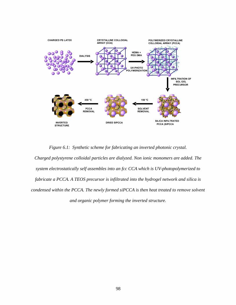
98
Figure 6.1: Synthetic scheme for fabricating an inverted photonic crystal.
Charged polystyrene colloidal particles are dialyzed. Non ionic monomers are added. The
system electrostatically self assembles into an fcc CCA which is UV-photopolymerized to
fabricate a PCCA. A TEOS precursor is infiltrated into the hydrogel network and silica is
condensed within the PCCA. The newly formed siPCCA is then heat treated to remove solvent
and organic polymer forming the inverted structure.

6.2.2 Preparation of PCCA
The highly-charged, non-cross-linked, monodisperse polystyrene colloids (Figure 6.1) used to
fabricate the siPCCA were prepared by emulsion polymerization.[53] The colloidal particle
size as measured by TEM is 180 nm ± 4nm. The colloidal particles were cleaned by dialysis
against deionized water followed by shaking with mixed bed ion-exchange resin (Bio-Rad
AG501-X8 (D)) In a typical PCCA recipe 2,2-hydroxyethyl methacrylate (6 g, 4.6×10⁻² mol,
Polysciences) and polyethylene glycol dimethacrylate (0.174 g, 5.3×10⁻⁴ mol, Polysciences)
were mixed together in a 2 dram vial. Aluminum oxide was added to remove the inhibitor
contained in the monomer solutions. The solutions were centrifuged for 5 min to remove the
aluminum oxide. 0.5 g of the deinhibited monomer solution supernatant was added to 2 g of the
cleaned, highly charged colloidal particle dispersion.
The resulting mixture was shaken for 30 sec. 10% diethoxyacetophenone (DEAP; 10 µL,
3.84 µmol; Aldrich) was added to the mixture which was then vortexed for 30 sec. The mixture
was injected between two quartz plates separated by a 125 µm Parafilm spacer. UV-
photopolymerization was performed by using two UV mercury lamps (Black Ray) for 13 min.
The PCCA film was removed from the quartz cell and equilibrated in a deionized water bath.
99

6.2.3 Infiltration of Sol-gel Precursor
A silica sol-gel precursor solution was prepared using a 1:1:3 molar ratio of TEOS/EtOH/water
adjusted to a pH of 2 with concentrated HCl. The fabricated PCCA film template was immersed
into two ml of the precursor solution.
Polymerization and condensation of the TEOS occurred around and within the PCCA
hydrogel matrix over the course of 5 days, generating an alcogel within the PCCA template. The
silica network was allowed to age and strengthen for an additional five days before further
processing.
6.2.4 Solvent Removal
The silica sol-gel infiltrated PCCA was solvent-exchanged for one week in ethanol. This ethanol-
containing, silica-infiltrated PCCA (siPCCA) was then heated at 85 °C for 1 day, followed by
heating to 150 °C for 5 hrs to remove all solvent.
6.2.5 Polymer Removal
After solvent removal, the temperature was increased to 250 °C and held for 6 hours to melt the
polystyrene colloidal particles as shown in iFigure 6.2. Higher temperature treatment at 450 °C
removed all organic polymer materials, leaving behind only the infiltrated silica.[57] Upon
firing the sample cracked into small fragments consisting of monoliths approximately 2 mm on a
side.
100

6.2.6 Physical Measurements
Transmission electron microscopy was used to measure particle size. We used a Phillips FEG
XL-30 FESEM operating in the ranges of 10–50 KeV to image the inverted structures.
Diffraction spectra were obtained at room temperature using an Ocean Optics USB2000
spectrophotometer with a six-around-one reflectance probe. Solvent refractive indices were
measured by using a Bausch & Lomb refractometer.
101
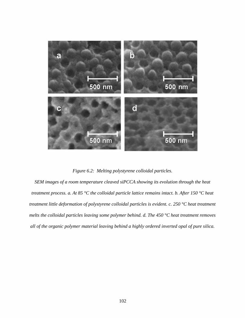
102
Figure 6.2: Melting polystyrene colloidal particles.
SEM images of a room temperature cleaved siPCCA showing its evolution through the heat
treatment process. a. At 85 °C the colloidal particle lattice remains intact. b. After 150 °C heat
treatment little deformation of polystyrene colloidal particles is evident. c. 250 °C heat treatment
melts the colloidal particles leaving some polymer behind. d. The 450 °C heat treatment removes
all of the organic polymer material leaving behind a highly ordered inverted opal of pure silica.

6.3 RESULTS AND DISCUSSION
6.3.1 Photonic Crystal Structure
Figure 6.2 shows four positions on a cleaved (111) surface of a silica filled PCCA (siPCCA)
sample at room temperature after heat treatments at 85 °C, 150 °C, 250 °C, and 450 °C. This
siPCCA was formed as shown in Figure 6.1 by polymerizing a hydrogel around a CCA, which
self-assembled due to the electrostatic repulsions between colloidal particles. The CCA generally
forms as a face centered cubic (fcc) lattice with a spacing determined by the particle number
density.
The hydrogel polymerizes around the fcc lattice without altering the CCA order. TEOS
was then infiltrated and condensed into the PCCA. Figure 6.2 a and bshow that the PCCA
colloidal lattice remains intact upon condensation of silica within the PCCA hydrogel matrix.
Some polystyrene particles have fallen out of the surface which proves that the PCCA hydrogel
embeds the CCA lattice and does not covalently attach to the colloidal particles.
Figure 6.2c shows the siPCCA after heat treatment at 250 °C, which exceeds the 240 °C
melting point of the non-cross-linked polystyrene.[74] The colloidal particles appear to have
significantly melted, leaving holes in the surface. The siPCCA at this stage turned brown
indicating that polymer degradation occurred. Energy dispersive x-ray analysis of the wall space
shows both silicon and carbon peaks indicating the presence of both organic material and the
infused silica.
103
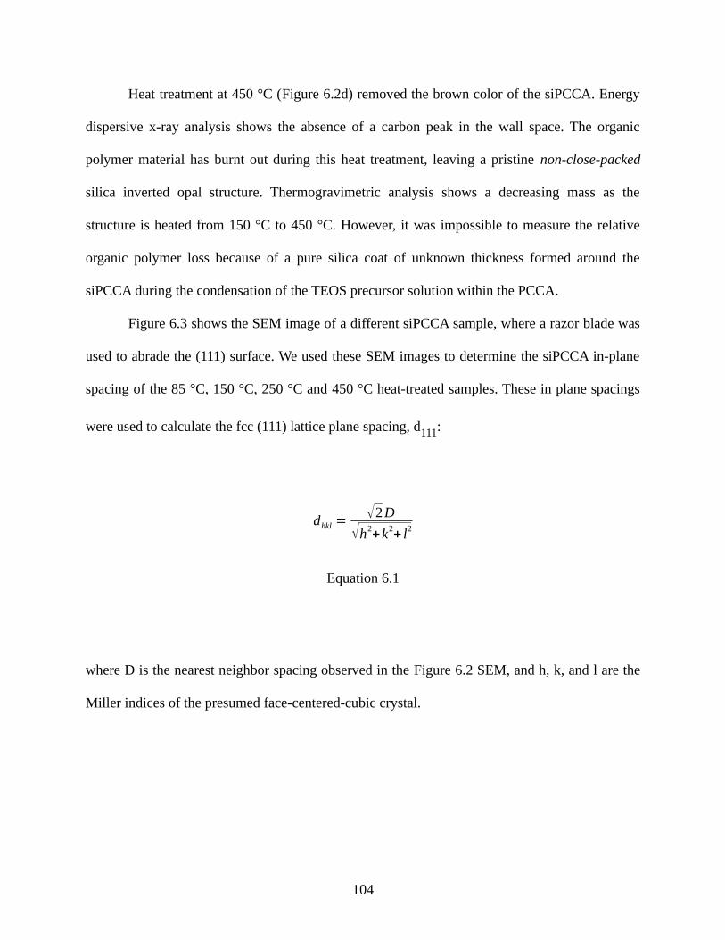
Heat treatment at 450 °C (Figure 6.2d) removed the brown color of the siPCCA. Energy
dispersive x-ray analysis shows the absence of a carbon peak in the wall space. The organic
polymer material has burnt out during this heat treatment, leaving a pristine non-close-packed
silica inverted opal structure. Thermogravimetric analysis shows a decreasing mass as the
structure is heated from 150 °C to 450 °C. However, it was impossible to measure the relative
organic polymer loss because of a pure silica coat of unknown thickness formed around the
siPCCA during the condensation of the TEOS precursor solution within the PCCA.
Figure 6.3 shows the SEM image of a different siPCCA sample, where a razor blade was
used to abrade the (111) surface. We used these SEM images to determine the siPCCA in-plane
spacing of the 85 °C, 150 °C, 250 °C and 450 °C heat-treated samples. These in plane spacings
were used to calculate the fcc (111) lattice plane spacing, d111:
where D is the nearest neighbor spacing observed in the Figure 6.2 SEM, and h, k, and l are the
Miller indices of the presumed face-centered-cubic crystal.
104
dhkl =√2 D
√h2+k2
+ l2
Equation 6.1
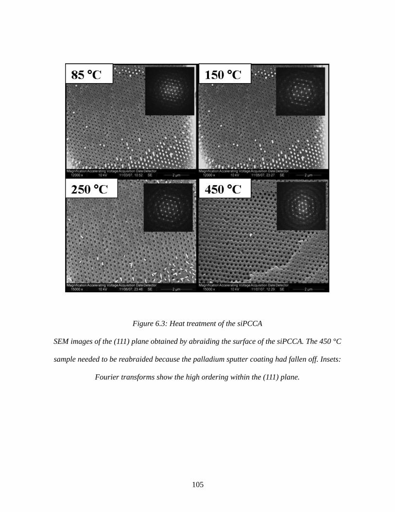
105
Figure 6.3: Heat treatment of the siPCCA
SEM images of the (111) plane obtained by abraiding the surface of the siPCCA. The 450 °C
sample needed to be reabraided because the palladium sputter coating had fallen off. Insets:
Fourier transforms show the high ordering within the (111) plane.
Abrasion of the siPCCA sample removes the silica coat as well as latex spheres. The
SEM derived (111) lattice plane spacing for the 85 °C and 150 °C heated samples were
essentially identical at 245±4 nm and 245±4 nm (mean ± SD) which indicates no decrease in
lattice constant upon heating. A slight decrease was calculated for the (111) lattice plane spacing
for the 250 °C (238±4 nm) and 450 °C (224±5 nm) heat treated samples. The ordering and
interparticle spacing which originated from the electrostatic formation of the original CCA
lattice, which was rigidified by formation of the PCCA and was set by the silica condensation, is
maintained throughout the heat treatment process.
Figure 6.4 shows the room temperature spectrum of the 180° back diffracted light for
light incident normal to the (111) surface of the heat treated siPCCA sample. The diffraction of
the siPCCA blue-shifts as the treatment temperature increases above 150 °C. Bragg’s law
(Equation 6.2) indicates that at a constant incident glancing angle a decrease in diffraction
wavelength requires a decrease in the average material refractive index, navg, or the d111 lattice
plane spacing, or both
where m is the order of diffraction, λ is the diffracted wavelength in air and θ is the glancing
angle of incidence. The average refractive index, navg, is approximately equal to the refractive
indices of the components, ni, weighted by their volume fractions, φi.
106
mλ = 2 d111navgsinθ
Equation 6.2

Substituting the SEM calculated d111 and the diffracted wavelength in Bragg’s law we can
calculate navg for each treated sample (Table 1). Clearly, the average refractive index decreases at
heat treatments of greater than 150 °C, indicating removal of the organic material.
107
navg =∑ n iφ i
Equation 6.3
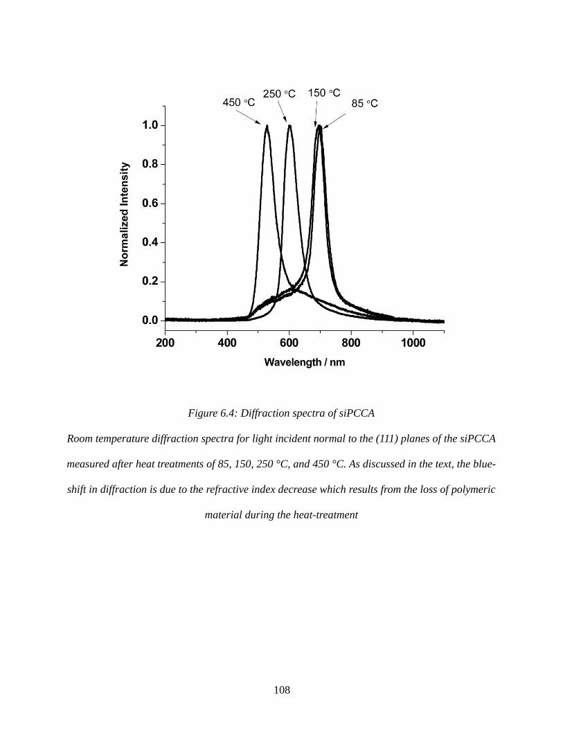
108
Figure 6.4: Diffraction spectra of siPCCA
Room temperature diffraction spectra for light incident normal to the (111) planes of the siPCCA
measured after heat treatments of 85, 150, 250 °C, and 450 °C. As discussed in the text, the blue-
shift in diffraction is due to the refractive index decrease which results from the loss of polymeric
material during the heat-treatment
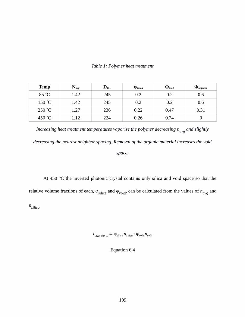
At 450 °C the inverted photonic crystal contains only silica and void space so that the
relative volume fractions of each, φsilica and φvoid, can be calculated from the values of navg and
nsilica
109
navg 450o C = φ silica nsilica+φ void nvoid
Equation 6.4
Table 1: Polymer heat treatment
Temp Navg D111 φsilica Φvoid Φorganic
85 ˚C 1.42 245 0.2 0.2 0.6
150 ˚C 1.42 245 0.2 0.2 0.6
250 ˚C 1.27 236 0.22 0.47 0.31
450 ˚C 1.12 224 0.26 0.74 0
Increasing heat treatment temperatures vaporize the polymer decreasing navg and slightly
decreasing the nearest neighbor spacing. Removal of the organic material increases the void
space.
The refractive index of silica in the inverted photonic crystal was determined by infusing
solvents[11] into the 450 °C pure silica sample in order to refractive index match the silica
which causes the diffraction to disappear (Figure 6.5a). For this experiment, an inverted siPCCA
was heat treated to 450 °C and the diffraction from a single region was monitored. We infused
the solvents for 24 hrs to achieve equilibrium. The diffraction disappears upon infiltration of
chloroform indicating that nsilica~1.45, the refractive index of CHCl3. Thus, using Equation 6.4,
we calculate φsilica = 26% for the 450 °C heat treated sample, giving a void volume fraction of
φvoid = 0.74.
Table 1 shows that navg decreases for the 250 °C sample, indicating loss of organic
polymer. Given a constant φsilica we can calculate the polymer and void volume fraction for all
of the samples by using Equation 6.5.
110
navg = φ silicansilica+φ void nvoid+φ polymer npolymer
Equation 6.5

111
Figure 6.5: Void volume of siPCCA
Study of void volume of siPCCA. a. Diffraction spectra obtained from the 450 °C heat treated
siPCCA in air and with solvent infiltrations of methanol, ethanol, chloroform, and toluene. b.
Linear best fit of the diffraction maxima of the 450 °C solvent infiltration data of a versus
solvent refractive index. c. SEM image showing wall porosity of siPCCA after 450 °C heat
treatment. d. Diffraction dependence on solvent refractive index for 250 °C heat treated sample

By assuming that the remaining polymer composition is identical to that of the original
PCCA we can estimate a volume average polymer refractive index, npolymer ~ 1.55. Table 1
shows that the 85 °C heat treated siPCCA has a ϕpolymer=0.6, which is ~50% greater than that of
the originally prepared PCCA. This occurs because, although the original PCCA swells after
exposure to the silica precursor solution, it then dramatically shrinks as the silica condenses
within the PCCA.
Table 1 shows that there is no loss of polymer for the 150 °C heat treated sample, but
almost half of the polymer is lost for the 250 °C heat treated sample. We calculate that the void
volume fraction of 20 % of the 85 and 150 °C heat treated samples almost doubles for the 250 °C
heat treated sample. The void volume fraction maximizes at 74% for the 250 °C heat treated
sample. It should be noted that we find a 20 % void volume fraction for the 85 °C heat treated
sample that results from evaporation of the solvent in the original silica condensed siPCCA. The
increased silica volume fraction for the 250 °C heat treated sample results from the volume
decrease of the siPCCA evident from the observed SEM decreased in-plane spacing as discussed
above. Our calculations of the volume fractions at the lower heat treatment temperatures took
cognizance of the calculated decrease in the (111) lattice plane spacing calculated from the SEM
data. We account for the change in silica volume fraction through the proportionality φsilicaV=φ
′silicaV′, where V is the original siPCCA volume and φ´silica and V´ are the silica volume fraction
and unit cell volume after heat treatment.
112
We can independently determine ϕsilica at 450 °C from a plot of the dependence of the
diffraction wavelength for normal incidence upon the refractive index of the infiltrated solvent
(Figure 6.5b). The slope of Equation 6.6 can be used to calculate ϕvoid and the intercept to
calculate ϕsilica.
Utilizing the derived (111) lattice plane spacing and the slope we determined a silica
filling fraction of φsilica = 17%, indicating a lower φsilica than calculated from the excellent
assumption that the diffraction wavelength in air can be simply related to the average siPCCA
refractive index given the SEM determined lattice spacing.
We conclude that the decreased slope calculated from Equation 6.6 results from sealed
voids which are inaccessible to the solvent. The SEM in Figure 6.5c shows the complex
morphology of the walls of the siPCCA. Obviously, the silica has condensed as particles which
are closely packed. It would not be surprising that part of the voids would be sealed off from
solvent infiltration.
To calculate the void volume inaccessible to solvent we can rewrite
113
λ = 2 d111 nsilicaφ silica+2 d111nsolvent φ void
Equation 6.6

where the total void volume is partitioned into inaccessible and accessible voids. From this
expression we calculate a 9% unfillable void space located in the silica wall space giving the
silica wall a ~35% porosity.
Figure 6.5d shows the results of solvent infiltrations into the 250 °C heat treated siPCCA
where some, but not all, of the polymer was removed. The diffraction spectrum in air is broad
and not symmetric and shows shoulders on both sides indicating a relatively inhomogeneous
siPCCA, in contrast to that of the Figure 6.5a 450 °C heat treated siPCCA. Infiltration of
methanol results in a very complex bandshape indicating a variable accessibility into this
siPCCA. In contrast, the bandshapes of the ethanol, isopropanol and water infiltrations are more
symmetric which indicates a chemical selectivity for solvent accessibility in the presence of
organic polymers. Peculiarly, the largest red-shift in diffraction results from methanol (shoulder),
which has the lowest refractive index. Obviously, there is some interesting interfacial chemical
selectivity present.
114
λ = 2 d111 nsilicaφ silica+2d111nsolvent φ accvoid+2 d111nairφ inaccvoid
Equation 6.7

6.3.2 Wall Spacing and Periodicity of siPCCA, Surface Morphology
The use of CCA electrostatic self-assembly enables the fabrication of fcc photonic crystal
materials where the nearest neighbor spacing can be defined independently of the interparticle
spacing. For inverse opal fcc crystals this allows us to independently control the fcc sphere void
spacing and the wall thickness as shown in Figure 6.6a and b which show two different siPCCA’s
made from identical colloidal particles, but where the lattice constant is varied by changing the
CCA particle number density. The decreased particle number density increases the wall thickness
and the silica wall volume fraction.
115
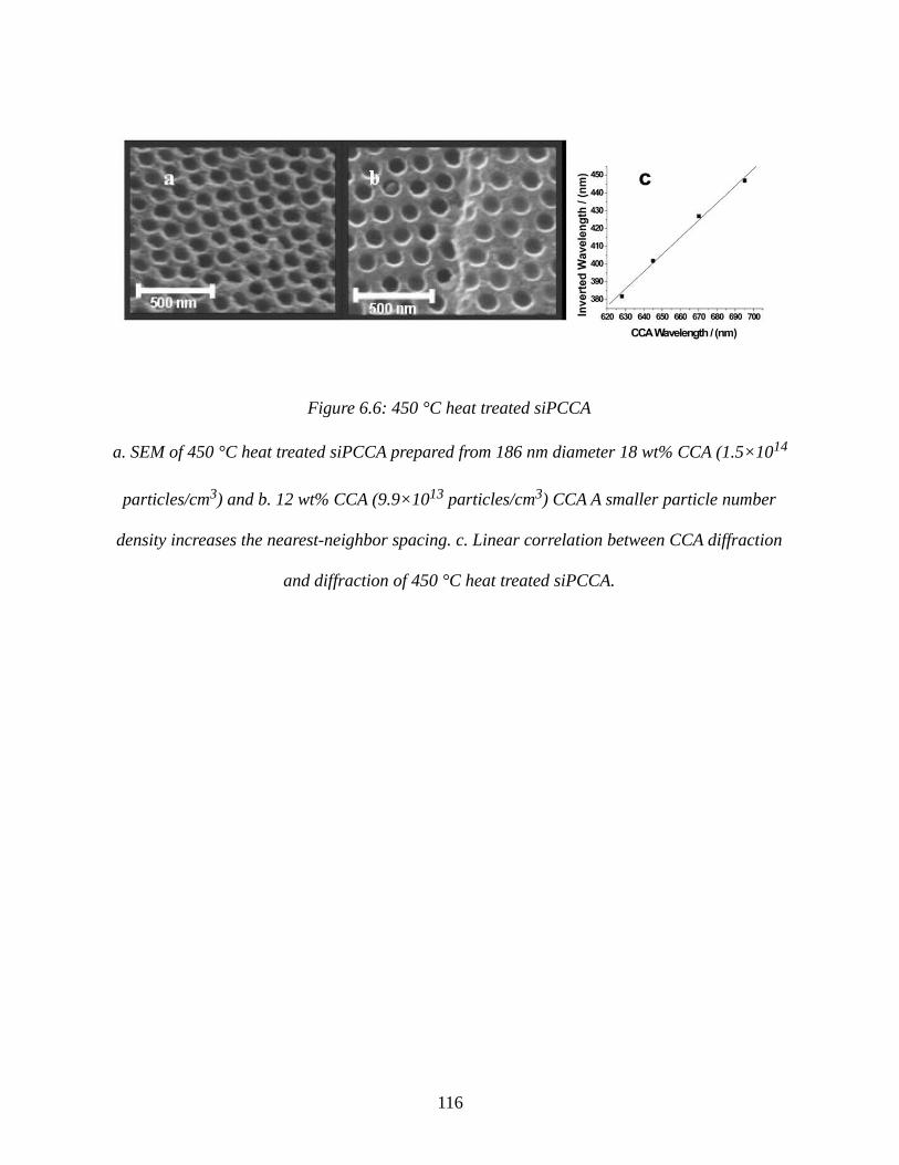
116
Figure 6.6: 450 °C heat treated siPCCA
a. SEM of 450 °C heat treated siPCCA prepared from 186 nm diameter 18 wt% CCA (1.5×10¹⁴
particles/cm3) and b. 12 wt% CCA (9.9×10¹³ particles/cm3) CCA A smaller particle number
density increases the nearest-neighbor spacing. c. Linear correlation between CCA diffraction
and diffraction of 450 °C heat treated siPCCA.
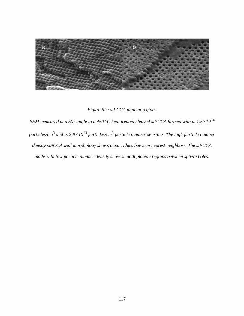
117
Figure 6.7: siPCCA plateau regions
SEM measured at a 50° angle to a 450 °C heat treated cleaved siPCCA formed with a. 1.5×10¹⁴
particles/cm3 and b. 9.9×10¹³ particles/cm3 particle number densities. The high particle number
density siPCCA wall morphology shows clear ridges between nearest neighbors. The siPCCA
made with low particle number density show smooth plateau regions between sphere holes.

Figure 6.6c, which demonstrates proportionality between the CCA diffraction and that of
the 450 °C heat treated siPCCA demonstrates that the original template CCA determines the
inverted siPCCA structure and spacing. In summary, the results above demonstrate that we have
developed a simple scalable, inexpensive process to create highly ordered photonic crystal
materials. We use electrostatically stabilized CCA as a template to form highly ordered siPCCA
and inverse opal silica photonic crystals, where the spacing and wall thickness can be
independently varied.
The Figure 6.7 SEM of inverted siPCCA inverse opal samples at high and low particle
density show clear differences in morphology of the cleaved surfaces. In contrast to the low
particle density surface which has plateaus between holes, the high particle number density
surface shows ridges between the originally close packed particles giving a hexagonal array of
bowl shaped cavities which may prove useful for future applications.
6.3.3 Ordering
As shown in the SEM photographs above and in Figure 6.8 the siPCCA and the inverse opal
photonic crystal materials are highly ordered over long ranges. Figure 6.8 shows an siPCCA
cleaved mainly along the 100 plane surfaces. The ordering of the SEM visually suggests high
order, possibly higher than that of the more typically studied close packed photonic crystal
materials made from colloidal particles with similar particle size monodispersities. The presumed
increased ordering of the siPCCA compared to close packed photonic crystals is expected from
the superior ordering of the original CCA template. The ordering of the CCA derives from soft
electrostatic repulsions between colloidal particles. Because of the soft repulsive interactions,
118
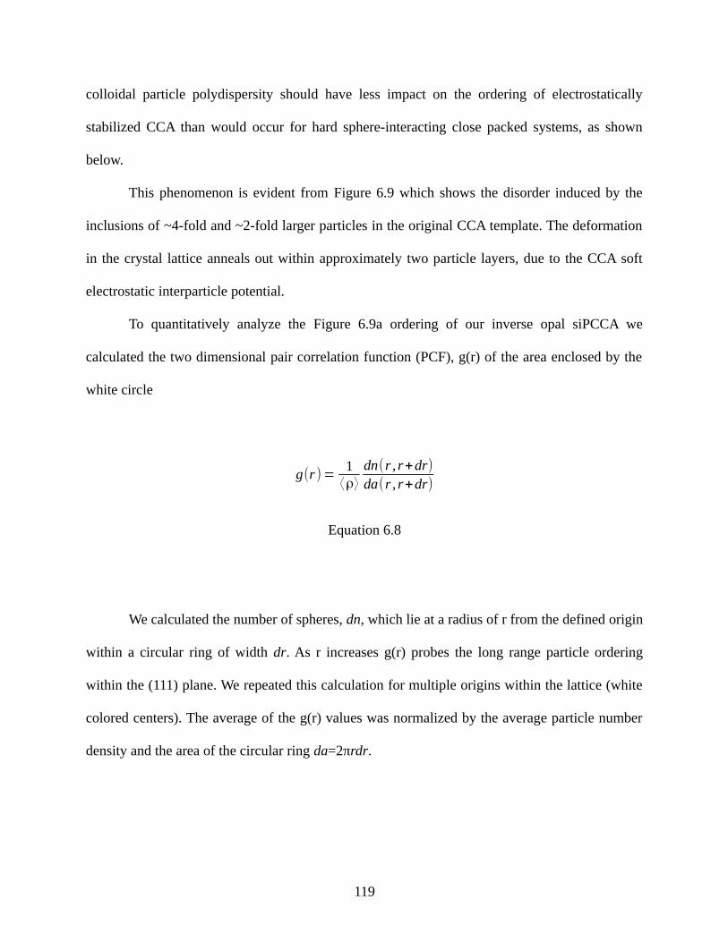
colloidal particle polydispersity should have less impact on the ordering of electrostatically
stabilized CCA than would occur for hard sphere-interacting close packed systems, as shown
below.
This phenomenon is evident from Figure 6.9 which shows the disorder induced by the
inclusions of ~4-fold and ~2-fold larger particles in the original CCA template. The deformation
in the crystal lattice anneals out within approximately two particle layers, due to the CCA soft
electrostatic interparticle potential.
To quantitatively analyze the Figure 6.9a ordering of our inverse opal siPCCA we
calculated the two dimensional pair correlation function (PCF), g(r) of the area enclosed by the
white circle
We calculated the number of spheres, dn, which lie at a radius of r from the defined origin
within a circular ring of width dr. As r increases g(r) probes the long range particle ordering
within the (111) plane. We repeated this calculation for multiple origins within the lattice (white
colored centers). The average of the g(r) values was normalized by the average particle number
density and the area of the circular ring da=2πrdr.
119
g(r )=1⟨ρ⟩
dn(r , r+dr)da(r , r+dr)
Equation 6.8

For well ordered crystals g(r) will be large for r values corresponding to multiples of the
in-plane (111) lattice constants. In contrast, g(r) will be small for intermediate r values. Colvin et
al recently showed highly ordered photonic crystal lattices generate g(r) showing many peaks
over large values of r which clearly indicate good long range ordering.[55]
120
121
Figure 6.8: siPCCA 100 planes
SEM of cleaved cross-section of low particle density siPCCA showing exposed 100 planes.
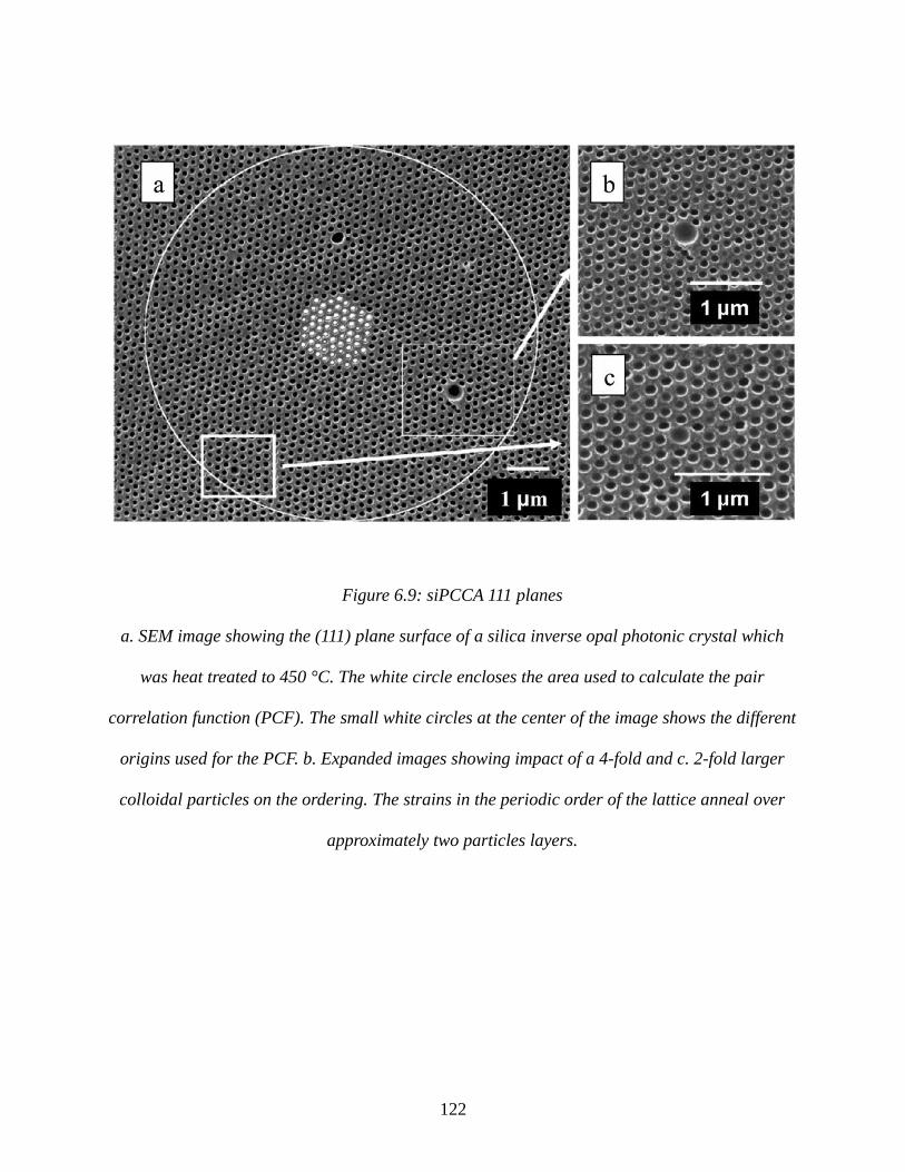
122
Figure 6.9: siPCCA 111 planes
a. SEM image showing the (111) plane surface of a silica inverse opal photonic crystal which
was heat treated to 450 °C. The white circle encloses the area used to calculate the pair
correlation function (PCF). The small white circles at the center of the image shows the different
origins used for the PCF. b. Expanded images showing impact of a 4-fold and c. 2-fold larger
colloidal particles on the ordering. The strains in the periodic order of the lattice anneal over
approximately two particles layers.
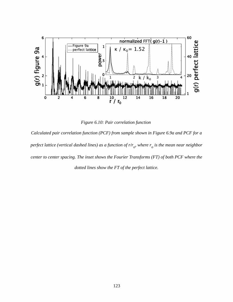
123
Figure 6.10: Pair correlation function
Calculated pair correlation function (PCF) from sample shown in Figure 6.9a and PCF for a
perfect lattice (vertical dashed lines) as a function of r/ro, where ro is the mean near neighbor
center to center spacing. The inset shows the Fourier Transforms (FT) of both PCF where the
dotted lines show the FT of the perfect lattice.
Figure 6.10 compares g(r) for the Figure 6.9a area within the white circle to g(r) of a
perfect (111) plane with the same average in-plane spacing and area. g(r) shows peaks out to r/ro
> 20 that coincide with those calculated for a perfect lattice, however, the g(r) siPCCA peak
amplitudes are smaller indicating a decreased ordering compared to the perfect lattice. The
Figure 6.10 inset shows the FT of g(r)-1 for the Figure 6.9 image. We calculate that κ/ κo = 1.52
demonstrating that our siPCCA is highly ordered. This high order occurs in spite of the presence
of multiple point defects. This ordering which results from simple CCA self assembly favorably
compares very favorably to the ordering found for convective self-assembled close-packed
photonic crystals.[55] Rengarajan et al [55] samples formed by convective self assembly of
3 to 4 % colloidal size distributions have average κ/ κo ~ 1.5, a value essentially identical to what
we obtained through electrostatic self assembly of the template.
We can qualitatively understand the decreased impact of particle polydispersity on CCA
ordering compared to that of close-packed particles by examining the interparticle repulsive
interactions. At present the electrostatic interaction between charged particles is modeled by
using DLVO theory.[9] We are aware that this is only a rough approximation since it is well
known that DLVO theory fails to describe particle repulsion for particles with high charge.[46]
Further the effective particle charge must be renormalized to significantly decrease the charge
density so that DLVO theory can successfully model electrostatic interactions for real colloidal
dispersions.[2]
The DLVO interaction potential, UDLVO(r) between particles with different sizes and
charges is:
124

where Z*1 and Z*
2 are the renormalized charges on two particles of radius a1 and a2. e is the
fundamental electronic charge, ε is the static dielectric constant of the medium and r is the
interparticle separation distance.[18] The Debye length, 1/κ, is given by
where kB is Boltzmann’s constant, np is the particle number density and ni is the ionic impurity
concentration. We presume that the system contains no added impurities, so that ni = 0. For the
discussion below we assume that a 10% variation in a single particle diameter and/or single
particle charge results in a negligible change in the Debye length of the system.
125
U DLVO(r) =Z1
* Z2* e2
ϵ[e
κa1
1+κa1 ][eκ a2
1+κ a2] e−κr
r
Equation 6.9
1/κ = √ 4π e2
ϵk BT[np Z*+ni]
Equation 6.10

The discussion below assumes a nominal colloidal particle diameter of 130 nm and a
renormalized charge of Z=1000. This charge renormalization corrects for extra charge screening
not included in DLVO theory. We choose for discussion a CCA nearest neighbor distance of 250
nm between particles, giving a particle number density of 1.613×10¹⁴ particles/cm3. We
calculate 1/κ for our system to be 10.4 nm.
Figure 6.11 shows that for this distance separation there is a negligible difference in the
DLVO potential in response to a 10 % increase in particle charge. Thus, changes in particle
charge must negligibly impact the CCA ordering at these nearest-neighbor distances.
126
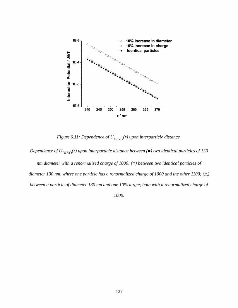
127
Figure 6.11: Dependence of UDLVO(r) upon interparticle distance
Dependence of UDLVO(r) upon interparticle distance between () two identical particles of 130
nm diameter with a renormalized charge of 1000; () between two identical particles of
diameter 130 nm, where one particle has a renormalized charge of 1000 and the other 1100; ( )
between a particle of diameter 130 nm and one 10% larger, both with a renormalized charge of
1000.

In contrast, Figure 6.11 shows that DLVO theory predicts a ~10 % increase in repulsive
interactions with a 10 % increase in the particle diameter. However, the porential energy
difference at the same interparticel spacing of 250nm is quite small, ~ 2 x 10⁻³ kBT per particle
This soft electrostatic repulsive potential prevents defect particles from significantly
impacting CCA ordering. We can roughly model the change which occurs in the interparticle
spacing brought on by a single defect particle with a 10 % increased particle diameter by
modeling the forces in a one dimensional array of particles that spans the characteristic photonic
crystal macroscopic size (Figure 6.12). We calculate the forces between particles, neglecting all
but nearest neighbor interactions, from the derivative of the DLVO potential with respect to
interparticle distance, r.
We assume a linear array of N particles. We compare the distance between particles for
an array of N identical particles which is x= L/ (N+1). When a single particle is replaced with a
defect particle having a 10% increase in diameter the particles expand around the defect particle
and contract around the other particles until the forces balance. This would result in a negligible
average particle spacing decrease for the other particles since this spacing difference would be
distributed over the other particles in the array.
128
F(r) =0 Z1 e Z2 e
ϵ [ eκ a1
1+κa1][ eκ a2
1+κa2][ 1+κ r
r2 ]e−k r
Equation 6.11

129
Figure 6.12: Model for response of one dimensional array of N particles to a single defect
particle
Model for response of one dimensional array of N particles to a single defect particle of
increased diameter. The N particles are arrayed along a cell of length L. In the top array the
particle diameters are identical and the system self assembles such that the spacings between
particles are identical at x = L / (N +1). In the bottom array one particle is replaced with a
particle of larger diameter. The distance between the larger diameter particle and the adjacent
particle is x1 = x + δ, while the distance between the other identical particles is x2 = L-2x1 /
(N−1). δ is determined by the equilibrium between forces.
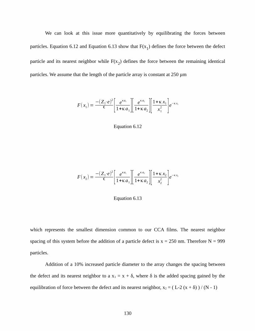
We can look at this issue more quantitatively by equilibrating the forces between
particles. Equation 6.12 and Equation 6.13 show that F(x1) defines the force between the defect
particle and its nearest neighbor while F(x2) defines the force between the remaining identical
particles. We assume that the length of the particle array is constant at 250 µm
which represents the smallest dimension common to our CCA films. The nearest neighbor
spacing of this system before the addition of a particle defect is x = 250 nm. Therefore N = 999
particles.
Addition of a 10% increased particle diameter to the array changes the spacing between
the defect and its nearest neighbor to a x1 = x + δ, where δ is the added spacing gained by the
equilibration of force between the defect and its nearest neighbor, x2 = ( L-2 (x + δ) ) / (N - 1)
130
F( x1)=−(Z1⋅e)2
ϵ [ eκa1
1+κa1][ eκ a2
1+κa2][1+κ x1
x12 ]e−κ x1
Equation 6.12
F( x2)=−(Z1⋅e)
2
ϵ [ eκa1
1+κa1][ eκ a2
1+κa2][1+κ x2
x22 ]e−κ x2
Equation 6.13
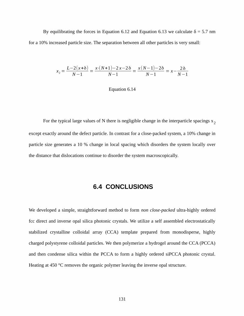
By equilibrating the forces in Equation 6.12 and Equation 6.13 we calculate δ = 5.7 nm
for a 10% increased particle size. The separation between all other particles is very small:
For the typical large values of N there is negligible change in the interparticle spacings x2
except exactly around the defect particle. In contrast for a close-packed system, a 10% change in
particle size generates a 10 % change in local spacing which disorders the system locally over
the distance that dislocations continue to disorder the system macroscopically.
6.4 CONCLUSIONS
We developed a simple, straightforward method to form non close-packed ultra-highly ordered
fcc direct and inverse opal silica photonic crystals. We utilize a self assembled electrostatically
stabilized crystalline colloidal array (CCA) template prepared from monodisperse, highly
charged polystyrene colloidal particles. We then polymerize a hydrogel around the CCA (PCCA)
and then condense silica within the PCCA to form a highly ordered siPCCA photonic crystal.
Heating at 450 °C removes the organic polymer leaving the inverse opal structure.
131
x2=L−2(x+δ)
N−1=
x⋅(N+1)−2 x−2δN−1
=x (N−1)−2δ
N−1= x−
2δN−1
Equation 6.14

This approach allows us to independently control the photonic crystal periodicity and size
of the basis of the fcc unit cell. We select the fcc lattice constant by defining the particle number
density of this electrostatically self assembled structure. Thus, we independently control the
spacing between particles. The particle diameter used determines the wall spacing of the inverse
opal photonic crystal and determines the shape of the photonic crystal dielectric constant
modulation. This allows us to optimize the diffraction of our photonic crystal structures.
These fcc photonic crystals simply and spontaneously self assemble due to their soft
electrostatic repulsion potentials. They show ordering as good or possibly better than close-
packed photonic crystals formed by convective assembly. We show that colloidal particle size
polydispersity has less impact on photonic crystal electrostatic ordering than occurs for ordering
of close-packed crystals. Point defect induced crystal strains in electrostatically stabilized CCA
anneal within ~two particle layers. We also show that charge polydispersity has only a small
impact on crystal ordering and that the strains due to defect particles of different charge also
anneal out over ~two particle layers.
132

6.5 BIBLIOGRAPHY
[1] Akahane, Y.; Asano, T.; Song, B.-S. and Noda, S. (2003). High-Q photonic nanocavity in a two-dimensional photonic crystal, Nature 425 : 944-947.
[2] Alexander, S.; Chaikin, P.; Grant, P.; Morales, G.; Pincus, P. and Hone, D. (1984). Charge renormalization, osmostic pressure, and bulk modulus of colloidal crystals: Theory, The Journal of Chemical Physics 80 : 5776-5781.
[3] Arsenault, A.; Fournier-Bidoz, S.; Hatton, B.; Míguez, H.; Tétreault, N.; Vekris, E.; Wong, S.; Yang, S.; Kitaev, V. and Ozin, G. (2004). Towards the synthetic all-optical computer: Science fiction or reality?, Journal of Materials Chemistry 14 : 781-794.
[4] Asher, S. (1986). US Patent 4,627,689.
[5] Asher, S. (1994). US Patent 5,281,370.
[6] Asher, S. (1995). US Patent 5,452,123.
[7] Asher, S.; Flaugh, P. and Washinger, G. (1986). Crystalline colloidal Bragg diffraction devices: The basis for a new generation of Raman instrumentation, Spectroscopy 1.
[8] Asher, S.; Holtz, J.; Liu, L. and Wu, Z. (1994). Self-assembly motif for creating submicron periodic materials. Polymerized crystalline colloidal arrays, Journal of the American Chemical Society 116 : 4997-4998.
[9] Belloni, L. (2000). Colloidal interactions, Journal of Physics Condensed Matter 12 : R549-R587.
[10] Blanco, A.; Chomski, E.; Grabtchak, S.; Ibisate, M.; John, S.; Leonard, S.; Lopez, C.; Meseguer, F.; Miguez, H.; Mondla, J.; Ozin, G.; Toader, O. and Van Driel, H. (2000). Large-scale synthesis of a silicon photonic crystal with a complete three-dimensional bandgap near 1.5 micrometres, Nature 405 : 437-440.
[11] Blanford, C.; Schroden, R.; Al-Daous, M. and Stein, A. (2001). Tuning solvent-dependent color changes of three-dimensionally ordered macroporous (3DOM) materials through compositional and geometric modifications, Advanced Materials 13 : 26-29.
[12] Busch, K. and John, S. (1998). Photonic band gap formation in certain self-organizing systems, Physical Review E - Statistical Physics, Plasmas, Fluids, and Related Interdisciplinary Topics 58 : 3896-3908.
133
[13] Carlson, R. J. and Asher, S. A. (1984). Characterization of optical diffraction and crystal structure in monodisperse polystyrene colloids., Applied Spectroscopy 38 : 297-304.
[14] Cheng, C. and Scherer, A. (1995). Fabrication of photonic band-gap crystals, Journal of Vacuum Science and Technology B: Microelectronics and Nanometer Structures 13 : 2696-2700.
[15] Chow, E.; Lin, S.; Johnson, S.; Villeneuve, P.; Joannopoulos, J.; Wendt, J.; Vawter, G.; Zubrzycki, W.; Hou, H. and Alleman, A. (2000). Three-dimensional control of light in a two-dimensional photonic crystal slab, Nature 407 : 983-986.
[16] Christodoulides, D.; Lederer, F. and Silberberg, Y. (2003). Discretizing light behaviour in linear and nonlinear waveguide lattices, Nature 424 : 817-823.
[17] Chutinan, A.; John, S. and Toader, O. (2003). Diffractionless flow of light in all-optical microchips, Physical Review Letters 90 : 123901/1-123901/4.
[18] Crocker, J. and Grier, D. (1996). When like charges attract: The effects of geometrical confinement on long-range colloidal interactions, Physical Review Letters 77 : 1897-1900.
[19] Davis, K.; Russel, W. and Glantschnig, W. (1991). Settling suspensions of colloidal silica: Observations and X-ray measurements, Journal of the Chemical Society, Faraday Transactions 87 : 411-424.
[20] Doosje, M.; Hoenders, B. and Knoester, J. (2000). Photonic bandgap optimization in inverted fee photonic crystals, Journal of the Optical Society of America B: Optical Physics 17 : 600-606.
[21] Fenollosa, R. and Meseguer, F. (2003). Non-close-packed artificial opals, Advanced Materials 15 : 1282-1285.
[22] Flaugh, P. L.; O'Donnell, S. E. and Asher, S. A. (1984). Development of a new optical wavelength rejection filter: Demonstration of its utility in raman spectroscopy., Applied Spectroscopy 38 : 847-850.
[23] Graugnard, E.; King, J.; Gaillot, D. and Summers, C. (2006). Sacrificial-layer atomic layer deposition for fabrication of non-close-packed inverse-opal photonic crystals, Advanced Functional Materials 16 : 1187-1196.
[24] Holtz, J. and Asher, S. (1997). Polymerized colloidal crystal hydrogel films as intelligent chemical sensing materials, Nature 389 : 829-832.
[25] Hoogenboom, J.; Derks, D.; Vergeer, P. and Van Blaaderen, A. (2002). Stacking faults in colloidal crystals grown by sedimentation, Journal of Chemical Physics 117 : 11320-11328.
[26] Imada, M.; Chutinan, A.; Noda, S. and Mochizuki, M. (2002). Multidirectionally distributed feedback photonic crystal lasers, Physical Review B - Condensed Matter and Materials Physics 65 : 1953061-1953068.
134
[27] Imada, M.; Lee, L.; Okano, M.; Kawashima, S. and Noda, S. (2006). Development of three-dimensional photonic-crystal waveguides at optical-communication wavelengths, Applied Physics Letters 88.
[28] Jiang, P.; Bertone, J.; Hwang, K. and Colvin, V. (1999). Single-crystal colloidal multilayers of controlled thickness, Chemistry of Materials 11 : 2132-2140.
[29] Joannopoulos, J.; Meade, R. and Winn, J. (1995). , Photonic crystals: Molding the flow of light .
[30] Joannopoulos, J.; Villeneuve, P. and Fan, S. (1997). Photonic crystals: Putting a new twist on light, Nature 386 : 143-149.
[31] John, S. (1987). Strong localization of photons in certain disordered dielectric superlattices, Physical Review Letters 58 : 2486-2489.
[32] Kesavamoorthy, G. and Asher, S. (1997). Optically nonlinear Bragg diffracting nanosecond optical switches, Physical Review Letters 78 : 3860-3863.
[33] Kesavamoorthy, R.; Super, M. and Asher, S. (1992). Nanosecond photothermal dynamics in colloidal suspension, Journal of Applied Physics 71 : 1116-1123.
[34] Kimble, K.; Walker, J.; Finegold, D. and Asher, S. (2006). Progress toward the development of a point-of-care photonic crystal ammonia sensor, Analytical and Bioanalytical Chemistry 385 : 678-685.
[35] King, J.; Galliot, D.; Graugnard, E. and Summers, C. (2006). Conformally back-filled, non-close-packed inverse-opal photonic crystals, Advanced Materials 18 : 1063-1067.
[36] Kitaev, V. and Ozin, G. (2003). Self-assembled surface patterns of binary colloidal crystals, Advanced Materials 15 : 75-78.
[37] Koh, Y. and Wong, C. (2006). In situ monitoring of structural changes during colloidal self-assembly, Langmuir 22 : 897-900.
[38] Krauss, T.; Song, Y.; Thoms, S.; Wilkinson, C. and DelaRue, R. (1994). Fabrication of 2-D photonic bandgap structures in GaAs/AlGaAs, Electronics Letters 30 : 1444-1446.
[39] Li, Z.-Y. and Zhang, Z.-Q. (2000). Fragility of photonic band gaps in inverse-opal photonic crystals, Physical Review B - Condensed Matter and Materials Physics 62 : 1516-1519.
[40] López, C. (2003). Materials aspects of photonic crystals, Advanced Materials 15 : 1679-1704.
[41] Maurer, M.; Lednev, I. and Asher, S. (2005). Photoswitchable spirobenzopyran-based photochemically controlled photonic crystals, Advanced Functional Materials 15 : 1401-1406.
[42] Meseguer, F. (2005). Colloidal crystals as photonic crystals, Colloids and Surfaces A: Physicochemical and Engineering Aspects 270-271 : 1-7.
135

[43] Meseguer, F. and Fenollosa, R. (2005). Non-close packed colloidal crystals, Journal of Materials Chemistry 15 : 4577-4580.
[44] Míguez, H.; López, C.; Meseguer, F.; Blanco, A.; Vázquez, L.; Mayoral, R.; Ocaña, M.; Fornés, V. and Mifsud, A. (1997). Photonic crystal properties of packed submicrometric SiO2 spheres, Applied Physics Letters 71 : 1148-1150.
[45] Míguez, H.; Tétreault, N.; Yang, S.; Kitaev, V. and Ozin, G. (2003). A new synthetic approach to silicon colloidal photonic crystals with a novel topology and an omni-directional photonic bandgap: Micromolding in Inverse Silica Opal (MISO), Advanced Materials 15 : 597-600.
[46] Naji, A.; Jungblut, S.; Moreira, A. and Netz, R. (2005). Electrostatic interactions in strongly coupled soft matter, Physica A: Statistical Mechanics and its Applications 352 : 131-170.
[47] Noda, S.; Fujita, M. and Asano, T. (2007). Spontaneous-emission control by photonic crystals and nanocavities, Nature Photonics 1 : 449-458.
[48] Noda, S.; Tomoda, K.; Yamamoto, N. and Chutinan, A. (2000). Full three-dimensional photonic bandgap crystals at near-infrared wavelengths, Science 289 : 604-606.
[49] Norris, D. (2007). Photonic crystals: A view of the future, Nature Materials 6 : 177-178.
[50] Painter, O.; Lee, R.; Scherer, A.; Yariv, A.; O'Brien, J.; Dapkus, P. and Kim, I. (1999). Two-dimensional photonic band-gap defect mode laser, Science 284 : 1819-1821.
[51] Pan, G.; Kesavamoorthy, R. and Asher, S. (1998). Nanosecond switchable polymerized crystalline colloidal array bragg diffracting materials, Journal of the American Chemical Society 120 : 6525-6530.
[52] Reese, C.; Baltusavich, M.; Keim, J. and Asher, S. (2001). Development of an intelligent polymerized crystalline colloidal array colorimetric reagent, Analytical Chemistry 73 : 5038-5042.
[53] Reese, C.; Guerrero, C.; Weissman, J.; Lee, K. and Asher, S. (2000). Synthesis of highly charged, monodisperse polystyrene colloidal particles for the fabrication of photonic crystals, Journal of Colloid and Interface Science 232 : 76-80.
[54] Reese, C.; Mikhonin, A.; Kamenjicki, M.; Tikhonov, A. and Asher, S. (2004). Nanogel nanosecond photonic crystal optical switching, Journal of the American Chemical Society 126 : 1493-1496.
[55] Rengarajan, R.; Mittleman, D.; Rich, C. and Colvin, V. (2005). Effect of disorder on the optical properties of colloidal crystals, Physical Review E - Statistical, Nonlinear, and Soft Matter Physics 71.
[56] Sanders, J. (1964). Colour of precious opal, Nature 204 : 1151-1153.
136
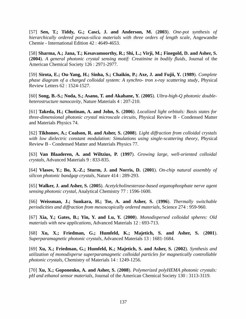
[57] Sen, T.; Tiddy, G.; Casci, J. and Anderson, M. (2003). One-pot synthesis of hierarchically ordered porous-silica materials with three orders of length scale, Angewandte Chemie - International Edition 42 : 4649-4653.
[58] Sharma, A.; Jana, T.; Kesavamoorthy, R.; Shi, L.; Virji, M.; Finegold, D. and Asher, S. (2004). A general photonic crystal sensing motif: Creatinine in bodily fluids, Journal of the American Chemical Society 126 : 2971-2977.
[59] Sirota, E.; Ou-Yang, H.; Sinha, S.; Chaikin, P.; Axe, J. and Fujii, Y. (1989). Complete phase diagram of a charged colloidal system: A synchro- tron x-ray scattering study, Physical Review Letters 62 : 1524-1527.
[60] Song, B.-S.; Noda, S.; Asano, T. and Akahane, Y. (2005). Ultra-high-Q photonic double-heterostructure nanocavity, Nature Materials 4 : 207-210.
[61] Takeda, H.; Chutinan, A. and John, S. (2006). Localized light orbitals: Basis states for three-dimensional photonic crystal microscale circuits, Physical Review B - Condensed Matter and Materials Physics 74.
[62] Tikhonov, A.; Coalson, R. and Asher, S. (2008). Light diffraction from colloidal crystals with low dielectric constant modulation: Simulations using single-scattering theory, Physical Review B - Condensed Matter and Materials Physics 77.
[63] Van Blaaderen, A. and Wiltzius, P. (1997). Growing large, well-oriented colloidal crystals, Advanced Materials 9 : 833-835.
[64] Vlasov, Y.; Bo, X.-Z.; Sturm, J. and Norris, D. (2001). On-chip natural assembly of silicon photonic bandgap crystals, Nature 414 : 289-293.
[65] Walker, J. and Asher, S. (2005). Acetylcholinesterase-based organophosphate nerve agent sensing photonic crystal, Analytical Chemistry 77 : 1596-1600.
[66] Weissman, J.; Sunkara, H.; Tse, A. and Asher, S. (1996). Thermally switchable periodicities and diffraction from mesoscopically ordered materials, Science 274 : 959-960.
[67] Xia, Y.; Gates, B.; Yin, Y. and Lu, Y. (2000). Monodispersed colloidal spheres: Old materials with new applications, Advanced Materials 12 : 693-713.
[68] Xu, X.; Friedman, G.; Humfeld, K.; Majetich, S. and Asher, S. (2001). Superparamagnetic photonic crystals, Advanced Materials 13 : 1681-1684.
[69] Xu, X.; Friedman, G.; Humfeld, K.; Majetich, S. and Asher, S. (2002). Synthesis and utilization of monodisperse superparamagnetic colloidal particles for magnetically controllable photonic crystals, Chemistry of Materials 14 : 1249-1256.
[70] Xu, X.; Goponenko, A. and Asher, S. (2008). Polymerized polyHEMA photonic crystals: pH and ethanol sensor materials, Journal of the American Chemical Society 130 : 3113-3119.
137

[71] Xu, X.; Majetich, S. and Asher, S. (2002). Mesoscopic monodisperse ferromagnetic colloids enable magnetically controlled photonic crystals, Journal of the American Chemical Society 124 : 13864-13868.
[72] Yablonovitch, E. (1987). , J. Phys., Colloq. C5.
[73] Zheng, Z.; Liu, X.; Luo, Y.; Cheng, B.; Zhang, D.; Meng, Q. and Wang, Y. (2007). Pressure controlled self-assembly of high quality three-dimensional colloidal photonic crystals, Applied Physics Letters 90.
[74] Dean, J. A. (Ed.), 1973. Lange's Handbook of Chemistry. McGraw-Hill, .
138

7.0 FABRICATION OF LARGE-AREA TWO-
DIMENSIONAL COLLOIDAL CRYSTALS
Author list: Jian-Tao Zhang, Luling Wang, Daniel N. Lamont, Sachin S. Velankar, and Sanford
A. Asher
Author Contribution: The author of this dissertation was responsible for characterizing the
degree of order of the photonic crystals, providing interpretation of the results and contributing
to the preparation of the manuscript. This work has been published as Angew Chem. Int. ed.
2012, 51, 6117
7.1 INTRODUCTION
Two-dimensional crystalline colloidal arrays (CCAs) have numerous applications, such as
photonic crystal materials and sensors[11-13; 22; 23; 26; 28; 29]. Recently,
numerous methods have been developed to prepare well-ordered 2D assemblies.[4; 6-8;
10; 24; 25] , These methods include spin coating, [6] dip coating,[7] and
electrophoretic deposition [24] of colloidal particles on planar substrates to form 2D
nanoparticle arrays. Particle assembly at interfaces can also be used to form 2D CCA
139

monolayers.[4; 8; 10; 25] 2D particle arrays have previously been prepared on water
surfaces.[9; 14; 17; 19; 27] For example, Giersig and co-workers reported on the self-
assembly of polystyrene (PS) latex particles on a water surface by applying a particle suspension
to a clean silicon wafer, immersing the silicon wafer in water, and then consolidating the particle
array by addition of surfactant. Through this method a few square centimeter 2D arrays were
obtained.[19] Retsch et al. used a similar approach to prepare close-packed 2D colloidal
crystals by floating and re-depositing colloidal monolayers at the air/water interface.[17] Qi
and co-workers modified this approach by dropping an aqueous ethanol particle suspension onto
a solid substrate that was surrounded by water. [9] The dispersion spread on the water surface,
resulting in monolayer 2D films up to about 16 cm2 in the area.[9] Pan et al. developed a
method to fabricate close-packed monolayer arrays of latex particles on a stirred water surface.
Then they transferred the arrays onto a substrate.[14] The maximum sizes of the 2D array
developed by the above methods appear limited to tens of square centimeters. There is a need to
develop methods to prepare 2D arrays of larger sizes.
For example, Jeong et al. reported a method to form large-area 2D arrays based on a
wire-wound rod coating method.[5] Recently, Vogel et al. presented a method to produce
close-packed monolayers by using a glass slide to add colloid suspensions to the air–water
interface. Close-packed monolayer patches crystallize upon spreading of an ethanolic PS colloid
dispersion. Upon further addition of colloid, the patches eventually assemble into a monolayer
covering the complete water surface.[21] Our group fabricated large 2D arrays by spreading
alcohol/water solutions of colloidal particles on top of mercury surfaces.[30; 31] We
obtained well-ordered 2D arrays by self-assembly of colloidal particles on mercury as the solvent
140

evaporated. These 2D arrays could easily be attached to hydrogel films.[30; 31] Although
this method was very successful in preparing large-area 2D arrays, the use of mercury as a
substrate is undesirable because of its toxicity.
Here, we report on fast fabrication of large 2D arrays of colloidal particles at the air/water
interface by a needle tip flow method. The preparation of the 2D monolayer CCAs by this
approach is illustrated in Figure 7.1a. The tip of a sharpened injection needle was positioned to
be just in contact with the water surface. The suspension was slowly and smoothly layered onto
the top of the water surface to form monolayer particle arrays. The spreading force of the
suspension drives the freshly formed particle array radially away from the needle tip to the outer
edge of the dish. A beautiful continuous 2D array monolayer filled the entire water surface
(>280 cm 2 in the current study, Equation 7.1b) in 2 min. The area of the resulting 2D arrays was
as large as the area of the water surface used. Many 2D array applications will benefit from the
ability to prepare large-area 2D arrays.
141
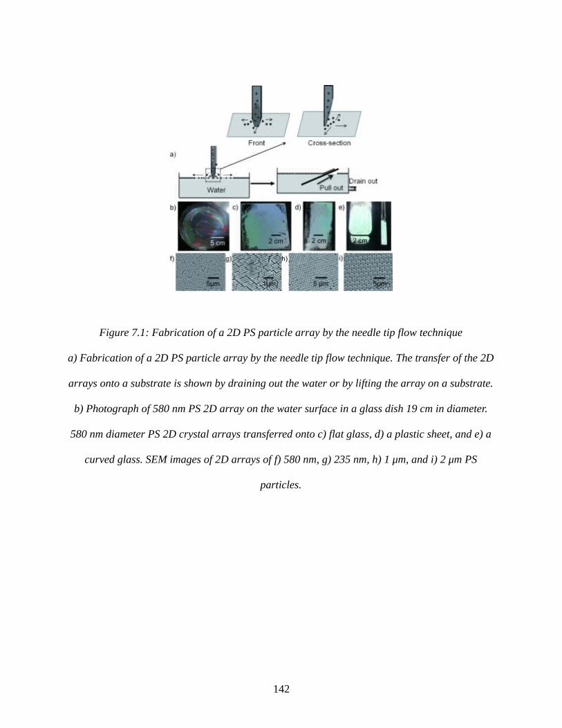
142
Figure 7.1: Fabrication of a 2D PS particle array by the needle tip flow technique
a) Fabrication of a 2D PS particle array by the needle tip flow technique. The transfer of the 2D
arrays onto a substrate is shown by draining out the water or by lifting the array on a substrate.
b) Photograph of 580 nm PS 2D array on the water surface in a glass dish 19 cm in diameter.
580 nm diameter PS 2D crystal arrays transferred onto c) flat glass, d) a plastic sheet, and e) a
curved glass. SEM images of 2D arrays of f) 580 nm, g) 235 nm, h) 1 μm, and i) 2 μm PS
particles.

7.2 RESULTS AND DISCUSSION
The spreading of the particle suspension uses the Marangoni effect in which a surface tension
gradient causes the liquid surface to be pushed away from the regions of low surface tension. In
the present case the Marangoni flow induced by adding the alcohol-containing colloidal
dispersion onto the water surface causes the colloidal particle dispersion to rapidly spread
outwards, thus covering the surface with particles.[3; 20]
The position of the needle tip is critically important for the formation of a 2D array on the
water surface. The contact of the needle tip with the water surface forms a meniscus structure
along the needle tip wall (Figure 7.1a). This meniscus damps the vertical flow forces to prevent
breaking of the water surface to enable the layering of the colloid dispersion on the water
surface.
As shown in Figure 7.1a we can transfer the floating 2D array onto a substrate by either
draining the water and settling the 2D array on the substrate, or by lifting the substrate and
depositing the 2D array on the substrate. Figure 7.1c-e show examples of 580 nm diameter PS
2D crystal arrays transferred onto a flat glass slide, a flat plastic sheet, and curved glass
substrates. Scanning electron microscopy (SEM) images show that the 2D arrays are hexagonally
close-packed. The arrays form hexagonal multi-domains of areas larger than 20 μm 2 (Figure
7.1f). Figure 7.1g, h, and i shows SEM images of 2D PS arrays with particle sizes ranging from
235 nm to 2 μm.
143
We conducted a quantitative analysis of the ordering of the 2D arrays shown in the SEM
images (Figure 7.1) by calculating the 2D pair correlation function, g(r) [1; 2; 16] , given in
Equation 7.1,
where a is the shell area and n(r,r+dr) is the number of particles that lie within the shell
considered. A SEM micrograph was first converted into a binary image, and then the MATLAB
image processing toolbox was used to locate the centroid of each particle. The bulk particle
density was calculated by dividing the total number of particles by the area of the polygon
formed by the particles inside the edges of the image boundaries. The curves of g(r) were
calculated between r=0.05 R0 to r=30 R0 using shell thicknesses of 0.016 R0, where R0 is the
particle radius and r is the distance from the origin of the radial distribution function and g(r) is
the calculated distance. To properly accommodate particles near the boundaries, a sub-routine
was used to determine the fraction of each g(r) integration shell within the image boundaries.
As previously reported, [2; 16] ,a quantitative measure of ordering is obtained from
the ratio of the full width at half maximum (FWHM), κ, of the first peak in the Fourier transform
of the function g(r)−1 to that of a perfectly ordered array, κ0. The ratio of κ/κ0=1 indicates a 2D
colloidal crystal that is essentially perfect in 2D structural ordering, whereas κ/κ0≤1.5 suggests a
144
g(r )=1⟨ p⟩
dn(r , r+dr )da(r , r+dr )
Equation 7.1

very highly ordered 2D structure; κ/κ0>1.5 indicates significant disordering.[16] Each SEM
image was measured against a perfect array with comparable period, image resolution, and
number of particles.
As shown in Figure 7.2a, g(r) shows a series of broad peaks that coincide with those
calculated for a perfect array. The peak intensities of g(r) decrease with the shell radius, r/2 R0,
which indicates that the 2D ordering decreases over long distances. The 2 and 1 μm PS arrays
exhibit significant correlation beyond the tenth normalized distance, r/2 R0. For the 235 nm PS
array, the correlation is not evident for r/2 R0>5. The κ/κ0 values, calculated for 2 μm, 1 μm, 580
nm and 235 nm PS arrays, are 1.01, 1.32, 1.70, and 2.59, respectively ( Figure 7.2b), which
indicates that the 2 μm PS array is nearly perfectly ordered, and the 1 μm array is highly ordered.
The ordering of 2D arrays decreases with the particle size. This is probably due to the fact
that the thinner particle arrays are less robust. The ordering of the small size particle 2D arrays
may have been disturbed by sample handling.
145

146
Figure 7.2: Pair correlation function.
a) Curves of g(r) calculated for 235 nm, 580 nm, 1 μm, and 2 μm PS particle arrays shown in
Figure 7.1. Horizontal black lines indicate g(r)=1. b) Single-sided power spectra Fourier
transforms (FT) of g(r) compared to FT of the corresponding perfectly ordered arrays. The
power spectra were scaled to have identical maxima at f/f0=1.

We modified our method to form 2D arrays on thin water films with the needle tip flow
technique (Figure 7.3a). After removing the water layer between the 2D array and the substrate,
the 2D array can be easily transferred onto a substrate. Figure 7.3 b and c shows photographs of
the 580 nm PS 2D arrays prepared on top of a glass and a plastic sheet. SEM images show that
the arrangement of 2D particles was also hexagonally close-packed and consisted of multi-
domains (Figure 7.3 d and e ), which are similar to the morphology of the 2D arrays prepared on
bulk water and then transferred onto substrates (Figure 7.1f).
147
Figure 7.3: Fabrication with substrate transfer
a) Fabrication of a 2D array on a flat substrate coated with a thin layer of water. Photographs
of thus prepared 2D 580 nm PS arrays on b) a glass and c) a plastic sheet. SEM images of 580
nm PS 2D arrays on d) a glass and e) a plastic sheet.

Using this approach, we fabricated 2D array patterns that contained patches of particles
of different sizes (Figure 7.4). We prepared a 490 nm PS 2D array patch first through the needle
tip flow method (Figure 7.4a) and then we used a dispersion of larger PS particles of 580 nm in
diameter to form a patch with a larger spacing in the middle (Figure 7.4b). These two particle
arrays display different diffraction colors (Figure 7.4d). We can imagine writing patterns of 2D
arrays for particular applications in displays, for chemical separations, and sensing.
148
Figure 7.4: Fabrication with two particle diameters.
Fabrication of a 2D array pattern formed with patches of two different particle diameters. a)
Spreading of a first particle array on water. b) Spreading of a second particle array. c) Resulting
2D array patterns on water. d) Visually observed diffraction of transferred 2D array pattern on a
glass substrate.
Our 2D particle arrays on substrates can be further functionalized and used for sensing
applications to visually detect analytes. As shown in Figure 7.5a we fabricated a thin hydrogel
film of 2D particles for pH sensing by depositing chitosan (CS, 2 wt %) that is dissolved in a 1
wt % acetic acid aqueous solution on a 2D particle array on a glass slide. We then evaporated the
solvents, washed the CS film with a 0.4 M aqueous NaOH solution to neutralize the acid, and
cross-linked the hydrogel in 0.5 wt % glutaraldehyde solution for 10 s. After washing with water,
we obtained a pH-sensitive 2D PS array hydrogel film (Figure 7.5b). Figure 7.5c shows the SEM
image of the 2D particles embedded in the dried CS hydrogel film.
We measured the diffraction in the Littrow configuration by using a six around one
reflection probe where we excite with white light the surrounding six fibers and collect the
diffracted light with the central fiber. The angle between the probe and the normal to the 2D
array sensor was about 32°. Figure 7.5d shows the diffraction spectrum of the 2D array CS films
at pH 7 (in pure water) and at pH 5 (in 2-( N-morpholino)ethanesulfonic acid, MES buffer
solution). At pH 7 diffraction is observed at 535 nm, whereas at pH 5 diffraction occurs at 645
nm. The CS hydrogel swells because of the protonation of its NH2 groups at pH 5. [18] The
CS hydrogel film swelling increases the particle lattice spacing of the 2D array, which red-shifts
the diffracted light. Figure 7.5e shows a photograph of the 2D array CS hydrogel film sensors on
a mirror surface that reflects the diffracted light.[31] The photograph clearly shows the green
and red colors of the diffracted light.
149
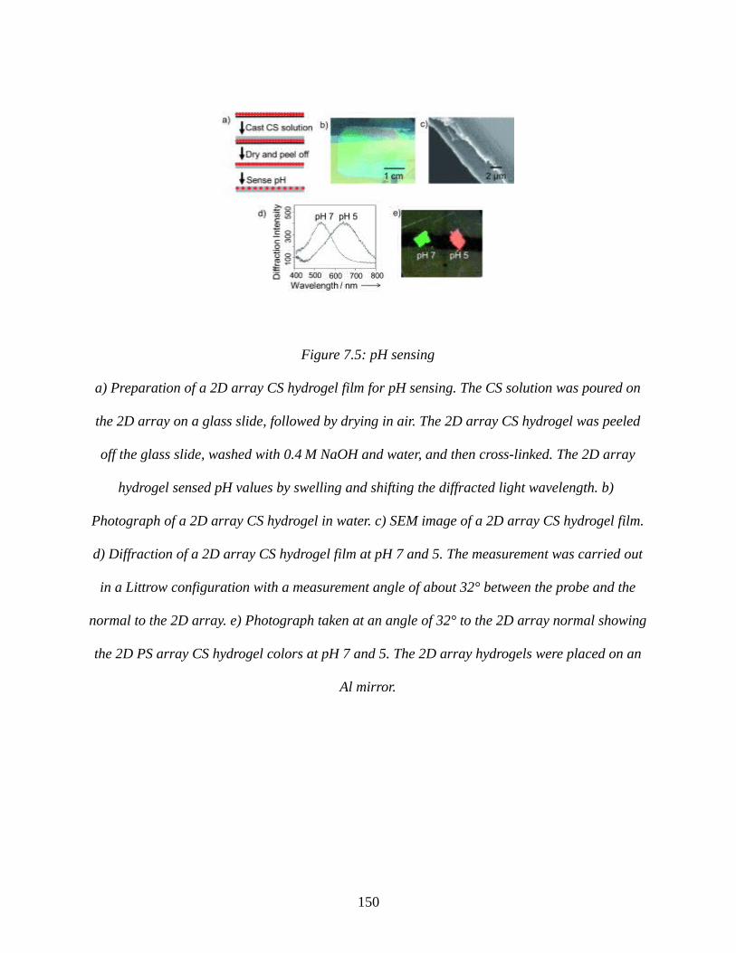
150
Figure 7.5: pH sensing
a) Preparation of a 2D array CS hydrogel film for pH sensing. The CS solution was poured on
the 2D array on a glass slide, followed by drying in air. The 2D array CS hydrogel was peeled
off the glass slide, washed with 0.4 M NaOH and water, and then cross-linked. The 2D array
hydrogel sensed pH values by swelling and shifting the diffracted light wavelength. b)
Photograph of a 2D array CS hydrogel in water. c) SEM image of a 2D array CS hydrogel film.
d) Diffraction of a 2D array CS hydrogel film at pH 7 and 5. The measurement was carried out
in a Littrow configuration with a measurement angle of about 32° between the probe and the
normal to the 2D array. e) Photograph taken at an angle of 32° to the 2D array normal showing
the 2D PS array CS hydrogel colors at pH 7 and 5. The 2D array hydrogels were placed on an
Al mirror.

In conclusion, we have developed a novel, simple, and efficient approach to rapidly
fabricate large-area 2D particle arrays on water surfaces. These arrays can easily be transferred
onto various substrates and functionalized for chemical sensing applications.
7.3 EXPERIMENTAL SECTION
Polystyrene (PS) particles with diameters of 490 and 580 nm were synthesized according to a
previously reported method.[15] The concentrations of 490 nm PS and 580 nm PS are 15 and
20 wt %, respectively, in water. The PS dispersion and propanol were mixed at a ratio of 2:1 in
volume and the mixture was vortexed for 1 min. Then the PS suspension was layered onto a
water surface using a syringe pump (Razel A99-FM, Razel Scientific Instruments, Inc.). To
transfer the 2D array onto a substrate, we lifted up the pre-placed substrate or drained the water
in the container.
The arrangement and morphology of the array was observed by using a scanning electron
microscope (SEM, Joel JSM6390LV) after sputter coating a thin layer of Au. Diffraction
measurements were conducted at a fixed angle using an Ocean Optics USB2000-UV-VIS
spectrometer, a LS-1 Tungsten Halogen Light Source and an R-series Fiber Optic Reflection
Probe. The hydrogels were equilibrated in water (pH 7) or in MES buffer solution (pH 5) and
then were put onto an Al glass mirror for diffraction measurements. The measurement was
carried out in the Littrow configuration with a measurement angle of about 32° between the
probe and the normal to the 2D array.
151

7.4 BIBLIOGRAPHY
[1] Allen, S. and Thomas, E., (1999). The Structure of Materials. Wiley.
[2] Bohn, J.; Ben-Moshe, M.; Tikhonov, A.; Qu, D.; Lamont, D. and Asher, S. (2010). Charge stabilized crystalline colloidal arrays as templates for fabrication of non-close-packed inverted photonic crystals, Journal of Colloid and Interface Science 344 : 298-307.
[3] Cai, Y. and Zhang Newby, B.-M. (2010). Polymeric microstructure arrays consequence of Marangoni flow-induced water droplets, Applied Physics A: Materials Science and Processing 100 : 1221-1229.
[4] Dimitrov, A.; Dushkin, G.; Yoshimura, H. and Nagayama, K. (1994). Observations of latex particle two-dimensional-crystal nucleation in wetting films on mercury, glass, and mica, Langmuir 10 : 432-440.
[5] Jeong, S.; Hu, L.; Lee, H.; Garnett, E.; Choi, J. and Cui, Y. (2010). Fast and scalable printing of large area monolayer nanoparticles for nanotexturing applications, Nano Letters 10 : 2989-2994.
[6] Jiang, P. and McFarland, M. (2004). Large-scale fabrication of wafer-size colloidal crystals, macroporous polymers and nanocomposites by spin-coating, Journal of the American Chemical Society 126 : 13778-13786.
[7] Kim, M.; Im, S. and Park, O. (2005). Fabrication and structural analysis of binary colloidal crystals with two-dimensional superlattices, Advanced Materials 17 : 2501-2505.
[8] Kondo, M.; Shinozaki, K.; Bergstroem, L. and Mizutani, N. (1995). Preparation of colloidal monolayers of alkoxylated silica particles at the air-liquid interface, Langmuir 11 : 394-397.
[9] Li, C.; Hong, G. and Qi, L. (2010). Nanosphere lithography at the gas/liquid interface: A general approach toward free-standing high-quality nanonets, Chemistry of Materials 22 : 476-481.
[10] Li, C.; Hong, G.; Wang, P.; Yu, D. and Qi, L. (2009). Wet chemical approaches to patterned arrays of well-aligned ZnO nanopillars assisted by monolayer colloidal crystals, Chemistry of Materials 21 : 891-897.
[11] Li, F.; Josephson, D. and Stein, A. (2011). Colloidal assembly: The road from particles to colloidal molecules and crystals, Angewandte Chemie - International Edition 50 : 360-388.
152

[12] Li, F.; Josephson, D. and Stein, A. (2011). , Angew. Chem. 123 : 378-409.
[13] Li, Y.; Koshizaki, N. and Cai, W. (2011). Periodic one-dimensional nanostructured arrays based on colloidal templates, applications, and devices, Coordination Chemistry Reviews 255 : 357-373.
[14] Pan, F.; Zhang, J.; Cai, C. and Wang, T. (2006). Rapid fabrication of large-area colloidal crystal monolayers by a vortical surface method, Langmuir 22 : 7101-7104.
[15] Reese, C. and Asher, S. (2002). Emulsifier-free emulsion polymerization produces highly charged, monodisperse particles for near infrared photonic crystals, Journal of Colloid and Interface Science 248 : 41-46.
[16] Rengarajan, R.; Mittleman, D.; Rich, C. and Colvin, V. (2005). Effect of disorder on the optical properties of colloidal crystals, Physical Review E - Statistical, Nonlinear, and Soft Matter Physics 71.
[17] Retsch, M.; Zhou, Z.; Rivera, S.; Kappl, M.; Zhao, X.; Jonas, U. and Qin, L. (2009). Fabrication of large-area, transferable colloidal monolayers utilizing self-assembly at the air/water interface, Macromolecular Chemistry and Physics 210 : 230-241.
[18] Ruel-Gariépy, E. and Leroux, J. (2006). 12. In: (Ed.), Chitosan: A Natural Polycation with Multiple Applications, American Chemical Society.
[19] Rybczynski, J.; Ebels, U. and Giersig, M. (2003). Large-scale, 2D arrays of magnetic nanoparticles, Colloids and Surfaces A: Physicochemical and Engineering Aspects 219 : 1-6.
[20] Scriven, L. and Sternling, C. (1960). The Marangoni effects, Nature 187 : 186-188.
[21] Vogel, N.; Goerres, S.; Landfester, K. and Weiss, C. (2011). A convenient method to produce close- and non-close-packed monolayers using direct assembly at the air-water interface and subsequent plasma-induced size reduction, Macromolecular Chemistry and Physics 212 : 1719-1734.
[22] Xia, D.; Ku, Z.; Lee, S. and Brueck, S. (2011). Nanostructures and functional materials fabricated by interferometric lithography, Advanced Materials 23 : 147-179.
[23] Xia, Y.; Gates, B.; Yin, Y. and Lu, Y. (2000). Monodispersed colloidal spheres: Old materials with new applications, Advanced Materials 12 : 693-713.
[24] Xie, R. and Liu, X.-Y. (2008). Electrically directed on-chip reversible patterning of two-dimensional tunable colloidal structures, Advanced Functional Materials 18 : 802-809.
[25] Yamaki, M.; Matsubara, K. and Nagayama, K. (1993). A thin liquid layer on the surface of mercury as a matrix of a flow-mediated two-dimensional assembly of proteins, Langmuir 9 : 3154-3158.
[26] Yang, S.-M.; Jang, S.; Choi, D.-G.; Kim, S. and Yu, H. (2006). Nanomachining by colloidal lithography, Small 2 : 458-475.
153

[27] Yu, J.; Yan, Q. and Shen, D. (2010). Co-self-assembly of binary colloidal crystals at the air - Water interface, ACS Applied Materials and Interfaces 2 : 1922-1926.
[28] Zhang, J.; Li, Y.; Zhang, X. and Yang, B. (2010). Colloidal self-assembly meets nanofabrication: From two-dimensional colloidal crystals to nanostructure arrays, Advanced Materials 22 : 4249-4269.
[29] Zhang, J. and Yang, B. (2010). Patterning colloidal crystals and nanostructure arrays by soft lithography, Advanced Functional Materials 20 : 3411-3424.
[30] Zhang, J.-T.; Wang, L.; Chao, X. and Asher, S. (2011). Periodicity-controlled two-dimensional crystalline colloidal arrays, Langmuir 27 : 15230-15235.
[31] Zhang, J.-T.; Wang, L.; Luo, J.; Tikhonov, A.; Kornienko, N. and Asher, S. (2011). 2-D array photonic crystal sensing motif, Journal of the American Chemical Society 133 : 9152-9155.
154
8.0 SPECTROSCOPY INTRODUCTION
8.1 INTRODUCTION
Fluorescence spectroscopy and related techniques are pervasive in many branches of science and
are applicable to many different types of chemical systems. Fluorescence measurements can
provide a wide range of information and insight into molecular processes, including solvent-
solute interaction, and the energetics of donor-acceptor systems. Steady-state and time-resolved
spectroscopy play a principle role in the investigations included in Chapters 9, 10 and 11. This
chapter presents a brief framework of the fundamental principles of fluorescence spectroscopy.
155
8.2 STEADY-STATE AND TIME-RESOLVED
FLUORESCENCE
Fluorescence measurements can be classified into a steady-state and time-resolved dichotomy. In
steady-state techniques a sample is illuminated with a constant illumination source and emission
intensity as a function of wavelength or spectrum, is detected. In time-resolved measurements a
pulsed light source allows the decay of fluorescence intensity to be recorded. Because
fluorescence processes typically occur on the nanosecond time scale, high-speed detection
systems and timing electronics are required in time-resolved measurements.
As noted by Lakowicz [2], steady-state observation records an average of the time-
resolved phenomena over the intensity decay of a sample, and much of the molecular
information is lost during this averaging process. However, many characteristics of a fluorophore
can be deduced from features in the steady-state fluorescence. For example, the sensitivity of a
fluorophore to solvent polarity can be determined from the Stoke shifts, which are more
pronounced in polar solvents.
Time-resolved measurements provide many types of molecular information. For example,
macromolecules can exist in more than a single conformation, and the decay time of a bound
probe may depend on conformation, with different decay times indicating different
conformations. When energy transfer is possible, the relative orientations of energy donors and
acceptors can be inferred.
156
8.3 FLUORESCENCE LIFETIMES AND QUANTUM YIELDS
The fluorescence lifetime and quantum yield are arguably the two most important characteristic
parameters for any type of fluorophore. The quantum yield is defined as the number of photons
emitted versus the number of photons absorbed; consequently, the brightest fluorophores have
quantum yields that approach unity. The fluorescence lifetime is a measure of the amount of time
a molecule spends in an excited state before returning to a ground state. Generally, fluorescence
lifetimes are on the order of 10 ns. Fluorescence emission is a stochastic process and can be
characterized by a radiate rate constant, Γ. The quantum yield and lifetime can be modified by
nonradiative processes, knr, that affect the overall lifetime and quantum yield.
In fluorescence experiments the number of excited molecules, n(t), is not directly
measured, but rather fluorescence intensity, which is proportional to n(t), is recorded. Assuming
the most elementary case, in which excited state decay processes are first order in the population
of the excited state, the decay of the excited state population is given by
dn (t)dt
= (Γ+knr)n (t)
Assuming that Γ and knr are time independent rate constants, the population of excited state
molecules, n(t), decays as n(t )= exp (−t / τ) where τ is the fluorescent lifetime and is given by
τ = (Γ+knr)−1 . Because the excited state decay is proportional to the intensity, we can write
I (t)= I 0 exp(−t / τ) , where I0 is the intensity at time 0. For a single exponential decay, the
157
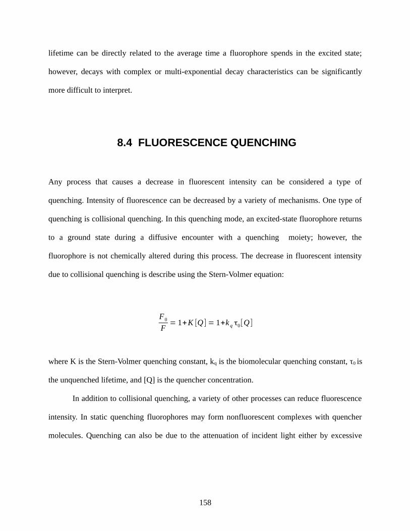
lifetime can be directly related to the average time a fluorophore spends in the excited state;
however, decays with complex or multi-exponential decay characteristics can be significantly
more difficult to interpret.
8.4 FLUORESCENCE QUENCHING
Any process that causes a decrease in fluorescent intensity can be considered a type of
quenching. Intensity of fluorescence can be decreased by a variety of mechanisms. One type of
quenching is collisional quenching. In this quenching mode, an excited-state fluorophore returns
to a ground state during a diffusive encounter with a quenching moiety; however, the
fluorophore is not chemically altered during this process. The decrease in fluorescent intensity
due to collisional quenching is describe using the Stern-Volmer equation:
F0
F= 1+K [Q ] = 1+k q τ0[Q ]
where K is the Stern-Volmer quenching constant, kq is the biomolecular quenching constant, τ0 is
the unquenched lifetime, and [Q] is the quencher concentration.
In addition to collisional quenching, a variety of other processes can reduce fluorescence
intensity. In static quenching fluorophores may form nonfluorescent complexes with quencher
molecules. Quenching can also be due to the attenuation of incident light either by excessive
158

fluorophore concentration or the presence of an additional absorbing moiety. Additionally,
excited state reaction, molecular rearrangements and energy transfer are other mechanisms that
produce quenching.
Static and dynamic quenching require the fluorophore and quencher to be in direct
physical contact. In collisional quenching, contact between a quencher and a fluorophore in an
excited state returns the fluorophore to the ground state via a non-radiative process. In static
quenching a nonfluorescent complex is formed between a quencher and fluorophore. Excited
state stabilization due to the formation of charge-transfer complexes has been studied
extensively. Nonpolar solvents can enhance fluorescent emission intensity from excited charge-
transfer complexes called an exciplexs. In a polar solvent, exciplex emission is quenched due to
stabilization of the exciplex, which lowers the excited state energy. Model systems in which an
electron donor and electron acceptor are connected by a molecular bridge have been particularly
useful in understanding the dynamics of charge transfer. In Chapter 11 synthetic control of
stereo-centers allows modification of the donor-acceptor geometry in order to explore the role
solvents play in an electron transfer reaction.
8.5 RESONANCE ENERGY TRANSFER
In contrast to dynamic quenching and complex formation, which require close proximity
between a fluorophore and a quenching moiety, resonance energy transfer (RET) is a through-
space interaction that can occur over longer distances. RET mechanisms decrease intensity of a
“donor” chromophore by transferring excited state energy to an “acceptor” moiety, which would
then undergo its own excited state relaxation processes. This process intrinsically involves an
159

excited state. A prerequisite of RET is some degree of spectral overlap between the emission
spectrum of an energy donor and the absorption spectrum of an energy acceptor. There is no
intermediate photon in RET. Donor photons do not participate in RET, as this process is not
dependent on the absorption of donor photons by the acceptor. The rate of energy transfer, kt,
between donor and acceptor is determined by the donor-acceptor spectral overlap and distance.
The rate is described by
k t =1τd (
R0
r )6
where r is the donor to acceptor distance, R0 is the Förster distance, and τd is the lifetime of the
donor in the absence of energy transfer. Förster distances typically range from 15 to 60 Å and are
determined, in part, by the spectral overlap. The extent of donor quenching can be used to
determine donor to acceptor distance.
8.6 TIME-RESOLVED LIFETIME MEASUREMENTS
Time-resolved measurements frequently provide information that is not available in steady-state
measurements. An often cited example is RET between a donor-accept system in which the
donor emission is observed to be quenched 50%. It is impossible to tell from the steady-state
spectra if this level of quenching is due to half of the donor being completely quenched, all of the
donor being quenched 50%, or some combination of these two extremes. These cases are easily
distinguished by measurement of the donor lifetime. The time-resolved measurements presented
160

in the following works (Chapters 9, 10 and 11) are based on the time-domain method. In this
method a short pulse of light, significantly shorter than the fluorescent lifetimes to be measured,
is used to excite a sample. The time-dependent intensity profile is measured using fast photon
counting electronics, which are synchronized to the excitation pulse. Fluorophores emit at
random times during the intensity decay. Some fluorophores emit quickly following the
excitation pulse while others emit after a significantly longer time delay. The intensity decay is
formed by collecting a statistical average of many photon emissions. Fitting the intensity decay
to an exponential allows determination of the excited state lifetime. However, care must be taken
when interpreting intensity decays that exhibit multi-exponential decay, as the amplitude and
lifetime fitting parameters are interconnected with many possible solutions capable of
satisfactorily fitting experimental data .
When conducting time-resolved fluorescence measurements, significant effort must be
made in the fitting of intensity decay to lifetime models. Elucidation of this point is facilitated by
examining the nature of the time-resolved intensity signal.
8.6.1 Intensity Decay Laws
Since the 1970s, maturation of time-resolved fluorescence techniques has included numerous
methods of data analysis. An early analysis method that is still widely used today is the nonlinear
least squares procedure (NLLS). In NLLS the level of consistency of a model function, typically
composed of 1-3 exponentially decaying components, to experimental data is quantified. If the
model function is found to be satisfactorily consistent with the experimental data, best estimates
161
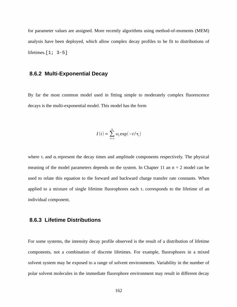
for parameter values are assigned. More recently algorithms using method-of-moments (MEM)
analysis have been deployed, which allow complex decay profiles to be fit to distributions of
lifetimes.[1; 3-5]
8.6.2 Multi-Exponential Decay
By far the most common model used in fitting simple to moderately complex fluorescence
decays is the multi-exponential model. This model has the form
I (t)=∑i=1
n
αi exp(−t / τi)
where τi and αi represent the decay times and amplitude components respectively. The physical
meaning of the model parameters depends on the system. In Chapter 11 an n = 2 model can be
used to relate this equation to the forward and backward charge transfer rate constants. When
applied to a mixture of single lifetime fluorophores each τ i corresponds to the lifetime of an
individual component.
8.6.3 Lifetime Distributions
For some systems, the intensity decay profile observed is the result of a distribution of lifetime
components, not a combination of discrete lifetimes. For example, fluorophores in a mixed
solvent system may be exposed to a range of solvent environments. Variability in the number of
polar solvent molecules in the immediate fluorophore environment may result in different decay
162
intensities. Additionally, due to the uncertainty in estimated parameter values, NLLS is not suited
to the analysis of multi-exponential decays containing closely spaced decay times. As is
demonstrated in Chapter 11, lifetime distribution fitting procedures can be used to partially
recover these closely spaced lifetimes.
8.7 APPLICATION OF FLUORESCENCE
Lanthanide metal ions display well-defined spectral emission lines that have long emission
lifetimes in aqueous solutions. The lanthanide emission results from nominally forbidden
transitions from the 4f orbitals; consequently, the emissive rate is very low, resulting in long
emission lifetimes typically in the range of 0.5 to 3 ms, and absorption coefficients are very low,
less than 10 M-1cm-1. Despite these limitations lanthanides are attractive fluorophores for
detection applications because the lanthanide emission has an extremely narrow line spectral
profile. In most applications, the low absorption cross-section requires lanthanides to be
complexed with some type of sensitizer. In Chapter 10 we show that ZnS nanoparticles can act as
an excitation antenna for a variety of different lanthanides that can be doped into the material.
Inorganic semiconductor nanoparticles (NP) exhibit a range of interesting material
characteristics. The bandgap can be tuned by varying the NP size. The net charge and solubility
can be modified by exchanging the surface capping ligands used to stabilize the inorganic core of
the NP. In Chapter 9, by studying the fluorescence quenching, we show that the direction of the
electric field created by electrostatic assemblies of oppositely charged cadmium selenide and
cadmium telluride nanoparticles can significantly alter the rate of photo-induced charge transfer
between the donor and acceptor nanoparticles.
163

In Chapter 11, photo-induced electron transfer is studied using bis-peptide molecules as
semi-rigid donor-bridge-acceptor scaffolds. Here, the importance of electron tunneling through
non-bonded contact is examined using steady-state fluorescence and lifetime distribution
analysis.
164

8.8 BIBLIOGRAPHY
[1] Dudewicz, E. J. and Van Der Meulen, E. C. (1981). Entropy-based tests of uniformity, Journal of the American Statistical Association 76 : 967-974.
[2] Lakowicz, J. R., 2007. Principles of Fluorescence Spectroscopy. Springer US, .
[3] Livesey, A. and Brochon, J. (1987). Analyzing the distribution of decay constants in pulse-fluorimetry using the maximum entropy method, Biophysical Journal 52 : 693.
[4] Merola, F.; Rigler, R.; Holmgren, A. and Brochon, J. C. (1989). Picosecond tryptophan fluorescence of thioredoxin: evidence for discrete species in slow exchange, Biochemistry 28 : 3383-3398.
[5] Vincent, M.; Brochon, J. C.; Merola, F.; Jordi, W. and Gallay, J. (1988). Nanosecond dynamics of horse heart apocytochrome c in aqueous solution as studied by time-resolved fluorescence of the single tryptophan residue (Trp-59), Biochemistry 27 : 8752-8761.
165
9.0 ELECTRON TRANSFER AND FLUORESCENCE
QUENCHING OF NANOPARTICLE ASSEMBLIES
Author list: Mingyan Wu, Prasun Mukherjee, Daniel N. Lamont and David H. Waldeck
Author contribution: The author of this dissertation contributed to the photophysical
characterization of the assemblies, interpretation of the results and the preparation of the
manuscript. This work has been published as J. Phys. Chem. C 2010 114, 5751
9.1 INTRODUCTION
Motivated by the increasing worldwide demand for clean energy resources, an effort is
being made to develop relatively cheap and highly efficient solar cells.[7; 33] Bulk
heterojunction (BHJ) solar cells, which are formed by the nanoscale phase separation of organic
materials, are one promising new platform for the development of low-cost photovoltaic (PV)
technology;[25; 51; 77] however, the power conversion efficiency of BHJ solar cells is
low compared to that of silicon-based p−n junction solar cells. The highest certified efficiency
for BHJ solar cells is now in the range of 6−7%, whereas the suggested maximum efficiency is in
the range of 10−12%.[22; 61] Improved efficiencies should be realized by better optimizing
166
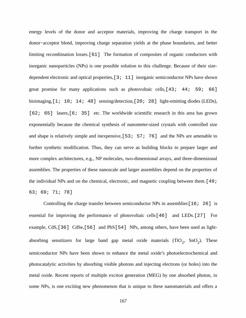
energy levels of the donor and acceptor materials, improving the charge transport in the
donor−acceptor blend, improving charge separation yields at the phase boundaries, and better
limiting recombination losses.[61] The formation of composites of organic conductors with
inorganic nanoparticles (NPs) is one possible solution to this challenge. Because of their size-
dependent electronic and optical properties,[3; 11] inorganic semiconductor NPs have shown
great promise for many applications such as photovoltaic cells,[43; 44; 59; 66]
bioimaging,[1; 10; 14; 48] sensing/detection,[20; 28] light-emitting diodes (LEDs),
[62; 65] lasers,[6; 35] etc. The worldwide scientific research in this area has grown
exponentially because the chemical synthesis of nanometer-sized crystals with controlled size
and shape is relatively simple and inexpensive,[53; 57; 76] and the NPs are amenable to
further synthetic modification. Thus, they can serve as building blocks to prepare larger and
more complex architectures, e.g., NP molecules, two-dimensional arrays, and three-dimensional
assemblies. The properties of these nanoscale and larger assemblies depend on the properties of
the individual NPs and on the chemical, electronic, and magnetic coupling between them.[49;
63; 69; 71; 78]
Controlling the charge transfer between semiconductor NPs in assemblies[16; 26] is
essential for improving the performance of photovoltaic cells[46] and LEDs.[27] For
example, CdS,[36] CdSe,[56] and PbS[54] NPs, among others, have been used as light-
absorbing sensitizers for large band gap metal oxide materials (TiO2, SnO2). These
semiconductor NPs have been shown to enhance the metal oxide’s photoelectrochemical and
photocatalytic activities by absorbing visible photons and injecting electrons (or holes) into the
metal oxide. Recent reports of multiple exciton generation (MEG) by one absorbed photon, in
some NPs, is one exciting new phenomenon that is unique to these nanomaterials and offers a
167
mechanism for dramatically improving the efficiency of NP-based solar cells.[18; 60]
Efficient charge transfer requires strong electronic coupling between the semiconductor NPs and
the metal oxide, and efficient charge separation requires favorable energetics (band alignment) to
inhibit back electron transfer.[21; 47; 50; 70; 74] Generally, closely packed
assemblies of NPs may be obtained in different ways, covalently or noncovalently, including
drop-casting,[5; 49] Langmuir methods,[24] cross-linking precipitation,[12; 38] and
stepwise self-assembly.[9; 41] The exploitation of electrostatic interactions has proved to be
a simple, effective approach for generating organized assemblies of charged NPs,[23; 31]
and this latter approach is used here.
Interfacial photoinduced charge transfer to metal NPs[32; 80] or dye/chromophore
molecules to semiconductor NPs has been extensively investigated.[26; 58; 64] Except for
the previously mentioned sensitization of TiO2 by NPs,[36; 54; 56] core−shell materials,
[34] and nanorod heterostructure materials,[17; 42] the charge transfer between
semiconductor NPs has drawn little attention, especially CdSe and CdTe, which are otherwise
extensively studied. Recently, Gross et al. studied the charge separation between thioglycolic
acid (TGA) capped CdTe and CdSe NP aggregates, achieved by the incorporation of divalent
Ca2+ ions between them.[23] Like that work, this study investigates charge transfer between
CdSe and CdTe NPs that have a type II band alignment. Instead of inducing association of
similarly charged NPs with divalent Ca2+ ions, the charge transfer assembly is formed by the
spontaneous self-assembly of the two oppositely charged NPs and can be manipulated by
variation of their surface charge. The NP compositions and sizes are chosen so that energy
transfer quenching is minimized and the charge transfer can be followed by the
168

photoluminescence (PL) quenching and lifetime shortening of the CdTe NPs by the CdSe NPs.
The magnitude of the PL quenching and lifetime shortening was found to depend on the
interparticle distance, relative NP sizes, and direction of the electric field created by the surface
charges.
9.2 EXPERIMENTAL DETAILS
9.2.1 Materials and Methods
Selenium powder (99.999%), tellurium powder (99.999%), cadmium chloride (CdCl2; 99%),
sodium borohydride (NaBH4; 98%), hexadecylamine (HDA; 99%), trioctylphosphine (TOP;
97%), trioctylphosphine oxide (TOPO; 90%), CdO (99.999%), 3-mercaptopropionic acid (MPA;
97%), N,N-dimethyl-2-aminoethanethiol hydrochloride (DEA; 95%), N,N,N-trimethyl-1-
dodecylammonium chloride (TDA; 99%), and N,N,N-trimethyl-2-aminoethane chloride (CEA;
99%) were purchased from Aldrich. N,N,N-trimethyl(11-mercaptoundecyl)ammonium chloride
(TMA; 98%) was purchased from ProChimia Surfaces (www.prochimia.com). See Figure 9.1 for
the structures of these compounds. All reagents and solvents were used as received. Water used
in all experiments was purified by a Barnstead Nanopure system, and its resistance was 18.2
MΩ-cm at 25 °C.
169
9.2.2 CdSe NP Synthesis and Ligand Exchange
TOPO-capped CdSe nanoparticles were prepared in a manner similar to a previously published
procedure.[53; 55] For a typical synthesis of CdSe nanoparticles, 0.0514 g (0.40 mmol) of
CdO, 0.1929 g (0.80 mmol) of HDA, and 3.8668 g (10.0 mmol) of TOPO were loaded into a 25
mL three-neck round-bottom flask. The mixture was heated to 300 °C under an Ar flow until
CdO was dissolved. A selenium stock solution (0.0787 g/1.0 mmol of selenium powder dissolved
in 4 mL of TOP) was then swiftly injected into the reaction flask. After the injection,
nanocrystals were allowed to grow at 280 °C until they reached the desired size. Highly
luminescent TOPO-capped CdSe NPs in a nonaqueous medium can be readily transferred to
water by the following procedure.[52; 68] About 20 mg of freshly prepared CdSe
nanocrystals was precipitated from toluene solution by adding methanol and then isolated by
centrifugation. The collected NPs were redissolved in chloroform. For preparing TMA-CdSe
170
Figure 9.1: Abbreviations, definitions, and structures

NPs, 2 mg of TMA was dissolved in 3 mL of chloroform and then added to the TOPO-CdSe
solution and the resulting solution stirred at room temperature in the dark for 1 h. The TMA-
CdSe NPs were gradually precipitated out of solution and then redispersed in water, providing a
clear homogeneous dispersion of NPs. The dispersion was purified by using three cycles of
concentration/dilution with an Ultrafree centrifugal filtration device (Millipore, MWCO 10,000).
These procedures should eliminate soluble organics and excess free ligands from the solution and
provide homogeneous aggregate-free NP dispersions that are ready for further use. To obtain
DEA-CdSe NPs, 50 mg of DEA was dissolved in 50 μL of water and added into the TOPO-CdSe
chloroform solution and the resulting solution stirred at room temperature in the dark for 1 h. The
surface-modified CdSe NPs were transferred into water and subsequently purified in a manner
similar to that used for the TMA-CdSe NPs. For preparing MPA-CdSe NPs, 20 mg of TOPO-
CdSe NPs and 100 μL of MPA were added into 3 mL of DMF. The mixture was heated to 60∼
°C in an oil bath for 2 h under an inert atmosphere to get a clear solution. Potassium tert-
butoxide ( 2 wt %) in DMF was added into the mixture to precipitate MPA-CdSe NPs. The∼
obtained CdSe NPs were collected by centrifugation and purified by ultrafiltration.
9.2.3 CdTe NP Synthesis
CdTe NPs were synthesized in aqueous solution, as described in a previously published
procedure.[57; 75] The surface charges were controlled to be either negative, by using MPA
as the capping ligand, or positive, by using DEA as the capping ligand. For example, MPA-CdTe
NPs, typically, were prepared as follows. First, 50.8 mg (0.4 mmol) of tellurium powder and 37.8
mg (1 mmol) of NaBH4 were loaded into a 25 mL two-necked flask and connected to a Schlenk
171
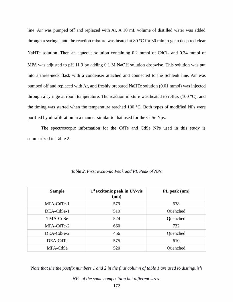
line. Air was pumped off and replaced with Ar. A 10 mL volume of distilled water was added
through a syringe, and the reaction mixture was heated at 80 °C for 30 min to get a deep red clear
NaHTe solution. Then an aqueous solution containing 0.2 mmol of CdCl2 and 0.34 mmol of
MPA was adjusted to pH 11.9 by adding 0.1 M NaOH solution dropwise. This solution was put
into a three-neck flask with a condenser attached and connected to the Schlenk line. Air was
pumped off and replaced with Ar, and freshly prepared NaHTe solution (0.01 mmol) was injected
through a syringe at room temperature. The reaction mixture was heated to reflux (100 °C), and
the timing was started when the temperature reached 100 °C. Both types of modified NPs were
purified by ultrafiltration in a manner similar to that used for the CdSe Nps.
The spectroscopic information for the CdTe and CdSe NPs used in this study is
summarized in Table 2.
172
Table 2: First excitonic Peak and PL Peak of NPs
Sample 1st excitonic peak in UV-vis
(nm)PL peak (nm)
MPA-CdTe-1 579 638
DEA-CdSe-1 519 Quenched
TMA-CdSe 524 Quenched
MPA-CdTe-2 660 732
DEA-CdSe-2 456 Quenched
DEA-CdTe 575 610
MPA-CdSe 520 Quenched
Note that the the postfix numbers 1 and 2 in the first column of table 1 are used to distinguish
NPs of the same composition but different sizes.

9.2.4 Steady-State Spectroscopy
Steady-state absorption spectra were measured on an Agilent 8453 spectrometer, and the steady-
state emission spectra were measured on a Horiba J-Y Fluoromax 3 fluorescence
spectrophotometer.
9.2.5 Time-Dependent Fluorescence Spectroscopy
The time-resolved fluorescence data were collected using the time-correlated single photon
counting (TCSPC) method.[39] The instrument response function was measured using a
sample of colloidal BaSO4. The samples were excited at 440 nm using a diode laser (PIL043,
ALS GmbH) and/or a 585 nm synchronously pumped dye laser at a 1 MHz repetition rate, and
6000 counts in the peak channel were collected for each sample. Experiments were also
performed with a 300 kHz repetition rate. Lifetime values were found to be nearly identical to
those collected at a 1 MHz repetition rate in all the systems studied. The fluorescence decay
curves were fit to a sum of exponentials by a convolution and compare method using IBH-DAS6
analysis software.[40]
173
9.2.6 Dynamic Light Scattering (DLS) and ζ Potential Measurements
DLS measurements were performed at room temperature in a 90° geometry and analyzed by
using particle sizing software with a 532 nm laser (Brookhaven Instrument Co.). The
electrophoretic mobility measurements were performed on the same instrument at room
temperature with an electrical field strength of 10 V/cm by using a Zeta Plus ζ potential analyzer.
9.3 RESULTS AND DISCUSSION
9.3.1 Formation of Aggregates Through Electrostatic Interaction
As shown in Figure 9.2, MPA-capped CdTe NPs in water show a first excitonic peak at 579 nm
(implying a size of about 3.5 nm in diameter[12] and the corresponding PL peak occurs at 638
nm (excitation wavelength at 400 nm). TOPO-capped CdSe NPs, which do not dissolve in water,
show a first excitonic peak at 518 nm in toluene (implying a size of about 2.5 nm in diameter)
and a corresponding photoluminescence peak at 531 nm.[12] After ligand exchange with TMA
or DEA, the CdSe NPs can be completely transferred into water and the absorbance maximum
shifts from 518 to 524 nm for TMA and from 518 to 519 nm for DEA. Other than this shift, the
spectra do not change significantly. The photoluminescence of the TMA-CdSe and the DEA-
CdSe NPs in water is strongly quenched, as compared to that for the TOPO-capped NPs in
toluene. The quenching is attributed to trapping states created during the ligand exchange process
174
of CdSe NPs with thiol molecules, as has been reported previously.[2] The absorption
spectrum of CdSe shows a very small overlap with the photoluminescence spectrum of the CdTe,
so that electronic energy transfer from the CdTe NPs to the CdSe NPs is negligible (see the
Supporting Information [75]).
175

176
Figure 9.2: Absorption and PL spectra of MPA-capped CdTe and TMA-capped CdSe NPs
Representative absorption and PL spectra of MPA-capped CdTe and TMA-capped CdSe NPs
used in this work: from left to right, CdSe absorbance in water after ligand exchange with TMA
(−−−), CdTe absorption in water (---), CdTe fluorescence in water (—). The quenched CdSe PL
is not shown.
Because of mutual electrostatic attraction, the negatively charged MPA-CdTe NPs and
positively charged TMA-CdSe NPs are expected to form aggregates under the appropriate
electrolyte solution conditions. The pKa value of DEA is about 10.5, so that the DEA-capped
CdSe is expected to be positively charged in aerated water (pH 6.6), and it can electrostatically
interact with the negatively charged MPA-CdTe. The aggregation was quantified by titrating the
positively charged TMA- or DEA-capped CdSe NPs into aqueous solutions of negatively
charged MPA-capped CdTe NPs, for which the CdTe final concentration was fixed at 0.9 × 10⁻⁶
M. Absorption spectra of these solutions show excitonic peaks of both CdSe and CdTe NPs and
are a superposition of the individual nanoparticle spectra, indicating that the electronic
transitions of the NPs remain isolated on the individual particles after mixing. DLS experiments
confirmed the presence of aggregates upon addition of TMA-CdSe (or DEA-CdSe) NPs to the
CdTe NP solutions. With increasing concentration of CdSe, the average diameters of the
aggregates grew from below 10 nm to on the order of 100 nm and reached a size on the order of
1−2 μm as the molar ratio of CdSe to CdTe approached 0.5 for the larger TMA-CdSe NPs and 1
for the smaller DEA-CdSe NPs. With a further increase in the concentration of positively
charged CdSe NPs, the aggregate size decreases to about 100 nm. See the Supporting
Information [75] for these data in tabular form.
ζ potential measurements (Figure 9.3) corroborate the DLS results. The initial ζ potential
for a solution of negatively charged MPA-CdTe NPs was about −21 mV. As the concentration of
TMA-CdSe NPs increased the ζ potential increased to about +1.1 mV at a CdSe/CdTe molar
ratio of 0.5 and then to about +28 mV at a molar ratio of 3. The addition of DEA-CdSe NPs to
CdTe NP solutions causes a similar trend but has a less sharp transition and asymptotes toward a
smaller positive potential.
177
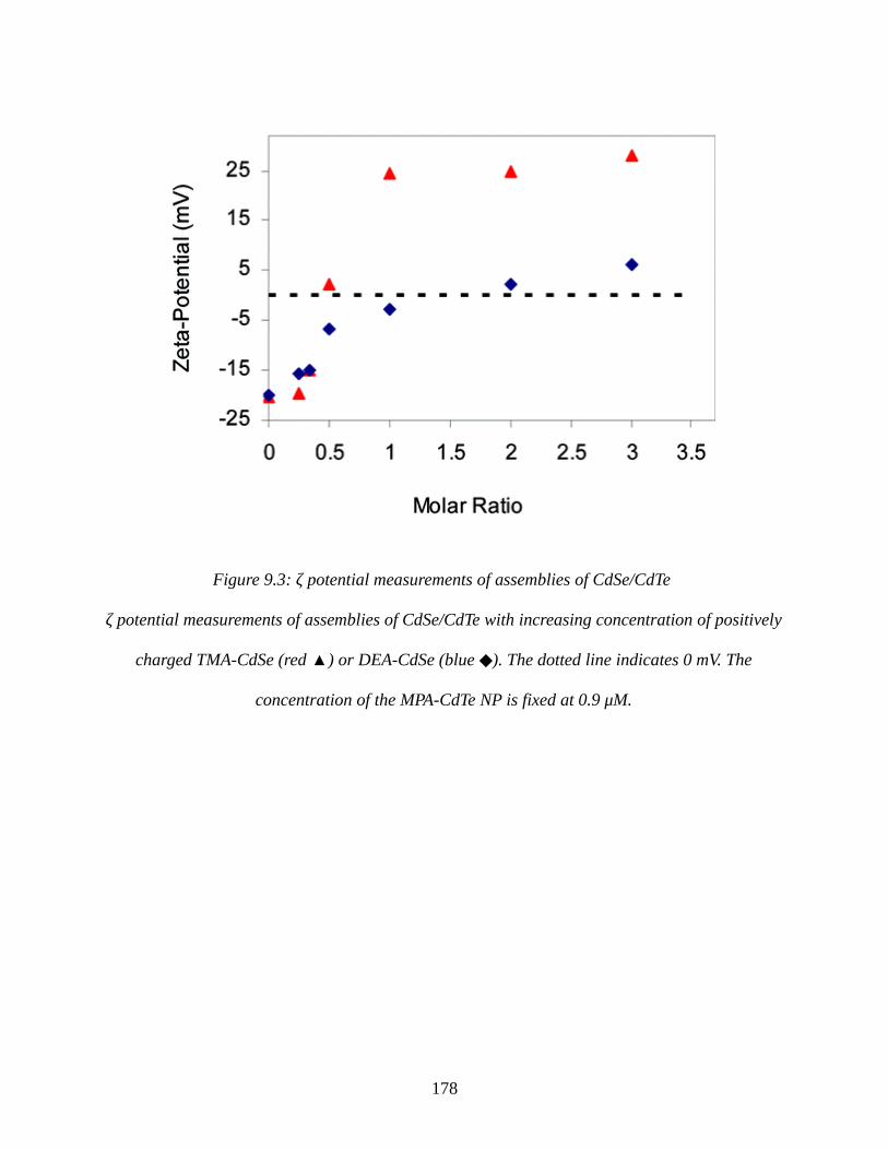
178
Figure 9.3: ζ potential measurements of assemblies of CdSe/CdTe
ζ potential measurements of assemblies of CdSe/CdTe with increasing concentration of positively
charged TMA-CdSe (red ) or DEA-CdSe (blue ). The dotted line indicates 0 mV. The
concentration of the MPA-CdTe NP is fixed at 0.9 μM.
These data indicate that as the proportion of positively charged TMA-CdSe NPs to
negatively charged MPA-CdTe NPs increases, aggregates form in the solution and the ζ potential
approaches zero. The concentration at which the aggregates are close to being neutral
corresponds to the concentration at which DLS gave the largest sizes. As the CdSe NP
concentration increases beyond this “isoelectric” point, the size decreases again because the
aggregates again have a net charge (albeit of opposite sign) that acts to inhibit the stability of
large aggregates. At a molar ratio of 3, the DLS results give an effective diameter of 130 nm∼
for the TMA-CdSe aggregates and 80 nm for the DEA-CdSe aggregates. The sharper ζ∼
potential change that is observed for TMA-CdSe may occur because more TMA ligands can be
loaded onto the CdSe NP surface as compared to DEA (because the longer TMA ligands reduce
electrostatic repulsion between neighboring ligands). This explanation can be rationalized from
the ζ potential values of pure TMA-CdSe NP solutions, +27 mV, and pure DEA-CdSe NP
solutions, about +13 mV.
9.3.2 Aggregation-Induced Self-Quenching Due to Interparticle
Interaction
Although the poor spectral overlap inhibits energy transfer quenching of CdTe NPs by CdSe
NPs, self-quenching of CdTe NPs can occur. Self-quenching is well-known for NP systems
where assembly in solution or the formation of a solid NP film from solution takes place, and it
can be attributed to electronic energy transfer from the smaller NPs to the larger NPs in the NP
size distribution.[15; 30; 37; 67] For a self-quenching NP solution, a red shift and
quenching of the photoluminescence can be observed as the NPs aggregate. To test for the
179
importance of self-quenching, the surfactant TDA, which has a positive headgroup and a length
similar to that of the TMA coating on the CdSe NPs, was titrated with a solution of the
negatively charged MPA-CdTe NPs. A 0.9 × 10⁻⁶ M solution of MPA-CdTe NPs in water
exhibits a strong photoluminescence peak around 638 nm; as TDA surfactant is added to the
solution, the emission peak red shifts to 672 nm. Furthermore, the photoluminescence intensity
quenches by a factor of 2 as the TDA/CdTe molar ratio increases from 0 to about 1 (assuming
there are about 350 MPA ligands per CdTe NP) and is saturated at this value for higher molar
ratios (see Figure 9.4b).[45] See the Supporting Information [75] for PL spectra. A similar
phenomenon is observed if the CdTe NP solution is titrated with TMA-capped CdSe NPs; the
emission’s peak wavelength red shifts and saturates at a value of 665 nm at high molar ratios (see
Figure 9.4a). We note that the red shift first appears to reach 671 nm at an intermediate mole
ratio (1:3 and 1:2 CdSe/CdTe) and then blue shifts back to 665 nm for a CdSe/CdTe molar ratio
of 3. Figure 9.4b shows that the final photoluminescence intensity quenches by a factor of about
2. The similarity of the red shift and PL quenching of the CdTe emission by the TMA-CdSe NPs
and TDA molecules indicates that the changes observed in the emission spectra arise from the
same self-quenching mechanism and is caused by interparticle interactions between CdTe NPs.
[15; 30; 37; 67] Other than driving the aggregation of CdTe NPs, the presence of TMA-
CdSe NPs does not provide a significant new nonradiative pathway for quenching.
180
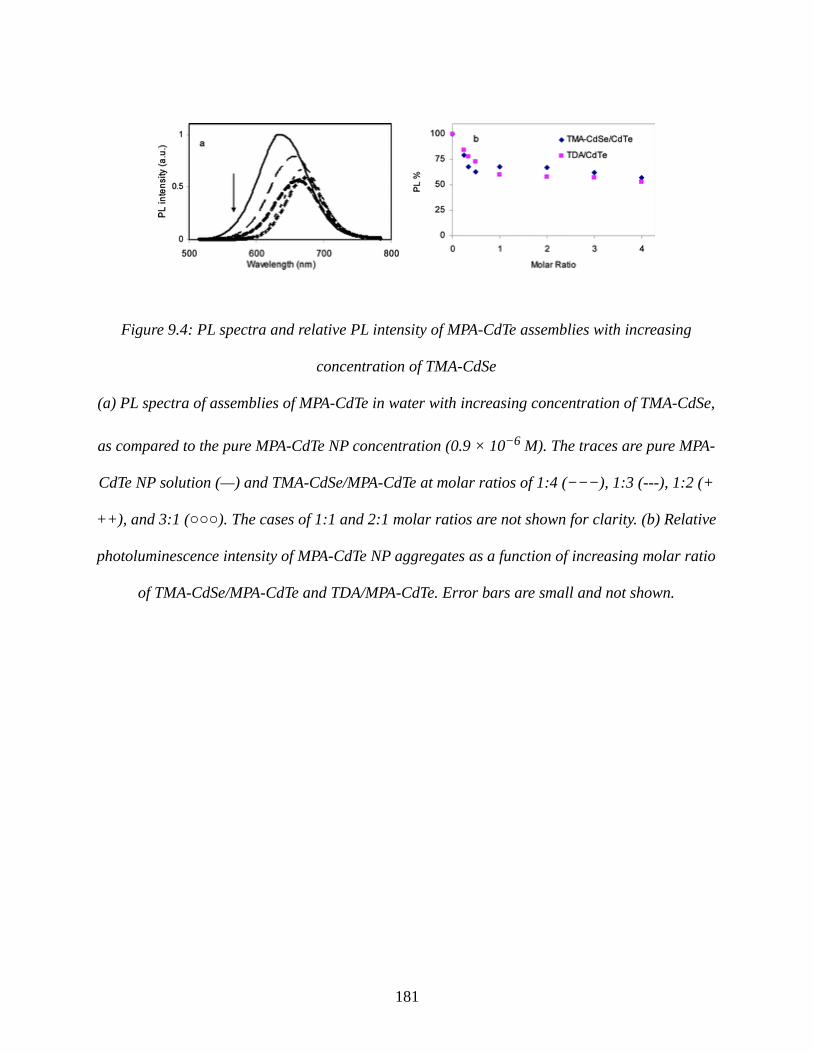
181
Figure 9.4: PL spectra and relative PL intensity of MPA-CdTe assemblies with increasing
concentration of TMA-CdSe
(a) PL spectra of assemblies of MPA-CdTe in water with increasing concentration of TMA-CdSe,
as compared to the pure MPA-CdTe NP concentration (0.9 × 10⁻⁶ M). The traces are pure MPA-
CdTe NP solution (—) and TMA-CdSe/MPA-CdTe at molar ratios of 1:4 (−−−), 1:3 (---), 1:2 (+
++), and 3:1 (). The cases of 1:1 and 2:1 molar ratios are not shown for clarity. (b) Relative
photoluminescence intensity of MPA-CdTe NP aggregates as a function of increasing molar ratio
of TMA-CdSe/MPA-CdTe and TDA/MPA-CdTe. Error bars are small and not shown.
9.3.3 Charge Transfer Process from CdTe to CdSe NPs
As shown above, the TMA-CdSe NPs, with their 11-methylene-thick surface coating, behave as
a surfactant that induces aggregation and self-quenching (a factor of 2) of the MPA-CdTe NPs.
Here we explore how the photoluminescence quenching of the MPA-CdTe NPs depends on the
thickness of the organic surface coating of the CdSe NPs, the relative energetics of the NPs, and
the direction of the interparticle electric field.
9.3.4 Interparticle Distance Dependence
In contrast to the weak (<50%) photoluminescence quenching of the MPA-CdTe NPs by TMA-
CdSe NPs, aggregates of MPA-CdTe NPs with DEA-CdSe NPs (containing only two
methylenes) give rise to a very significant (>98%) quenching (see Figure 9.5). For a molar ratio
of DEA-CdSe to MPA-CdTe that is less than 1, the PL intensity is quenched by about 30−40%
and the peak position is only slightly red-shifted. As the molar ratio increases to 2, the PL
intensity is quenched by more than 75% and the peak red shifts to 665 nm, and when the molar
ratio increases to 3 or larger, the PL intensity is quenched by more than 90% and the peak
emission wavelength shifts back to 656 nm.
182
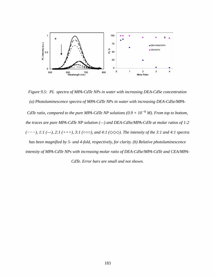
183
Figure 9.5: PL spectra of MPA-CdTe NPs in water with increasing DEA-CdSe concentration
(a) Photoluminescence spectra of MPA-CdTe NPs in water with increasing DEA-CdSe/MPA-
CdTe ratio, compared to the pure MPA-CdTe NP solutions (0.9 × 10⁻⁶ M). From top to bottom,
the traces are pure MPA-CdTe NP solution (—) and DEA-CdSe/MPA-CdTe at molar ratios of 1:2
(−−−), 1:1 (---), 2:1 (+++), 3:1 (), and 4:1 ( ). The intensity of the 3:1 and 4:1 spectra
has been magnified by 5- and 4-fold, respectively, for clarity. (b) Relative photoluminescence
intensity of MPA-CdTe NPs with increasing molar ratio of DEA-CdSe/MPA-CdTe and CEA/MPA-
CdTe. Error bars are small and not shown.

The quenching of MPA-CdTe NP photoluminescence by DEA-CdSe NPs was found to be
reversible. If 0.5 M NaCl was added to a solution of MPA-CdTe NPs, the PL peak remained in
the same spectral position as the original peak and a small amount of quenching ( 30%) was∼
observed (Figure 9.6a). Subsequent addition of DEA-CdSe NPs, to create a molar ratio of 4:1
with MPA-CdTe, did not induce more significant changes. Similarly if a high concentration of
NaCl is added into a solution of DEA-CdSe/MPA-CdTe, the emission’s peak wavelength blue
shifts back to the original CdTe peak position and the PL intensity recovers to the value found for
a NaCl containing solution of MPA-CdTe. These results imply that the NPs do not degrade upon
DEA-CdSe addition, nor do they cluster nonspecifically as a result of a high ionic strength of the
solution. In addition, this experiment confirms that the close proximity of DEA-CdSe is driven
by electrostatic attraction and is required for efficient photoluminescence quenching.
184
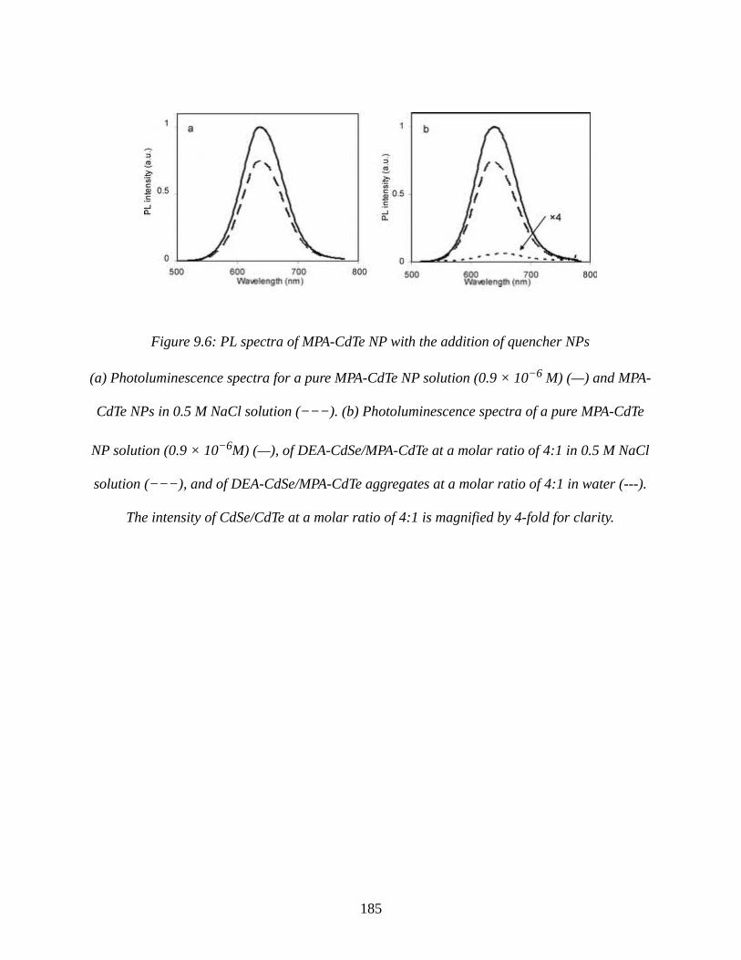
185
Figure 9.6: PL spectra of MPA-CdTe NP with the addition of quencher NPs
(a) Photoluminescence spectra for a pure MPA-CdTe NP solution (0.9 × 10⁻⁶ M) (—) and MPA-
CdTe NPs in 0.5 M NaCl solution (−−−). (b) Photoluminescence spectra of a pure MPA-CdTe
NP solution (0.9 × 10⁻⁶M) (—), of DEA-CdSe/MPA-CdTe at a molar ratio of 4:1 in 0.5 M NaCl
solution (−−−), and of DEA-CdSe/MPA-CdTe aggregates at a molar ratio of 4:1 in water (---).
The intensity of CdSe/CdTe at a molar ratio of 4:1 is magnified by 4-fold for clarity.
As a control experiment MPA-CdTe NPs were titrated by CEA, which has a chain length
similar to that of DEA and a positive headgroup like that of DEA. This experiment showed that
the photoluminescence spectra of CEA/MPA-CdTe do not change significantly (see the
Supporting Information [75]). A plot of the relative PL intensities of DEA-CdSe/MPA-CdTe
NPs and CEA/MPA-CdTe NPs (see Figure 9.5b) reveals the dramatic difference in quenching
efficiencies. The extent of aggregation and ζ potential changes in CEA/MPA-CdTe NP solutions
are very small. Clearly, the DEA-CdSe NPs are necessary to observe significant PL quenching,
and CEA molecules do not play a role in either inducing the aggregates or PL quenching.
In another control experiment the dendrimer PAMAM 2G (Dendritech, Inc.), which has
no visible chromophore, was used to induce aggregates of MPA-CdTe NPs. PAMAM 2G is 2.9
nm in diameter and has 16 NH2 surface groups which should be protonated in water at pH 6.6.
For a molar ratio of 3:1 (PAMAM 2G/MPA-CdTe), aggregates of several hundreds of
nanometers diameter were formed and the accompanying ζ potential changed from −21 to +36
mV. The PL peak red shifts to 670 nm, and the intensity quenches by 30−40% (see the UV−vis∼
and PL spectra in the Supporting Information [75]).
These experiments indicate that the DEA-CdSe NPs both enhance aggregate formation,
as evidenced by a more significant red shift in PL than the case of CEA ligands only, and cause
much stronger quenching, as compared to the PAMAM-2G dendrimer systems, which induce
aggregates of a size similar to those found for DEA-CdSe. The red shift for the DEA-
CdSe/MPA-CdTe NP solution is less than that observed for the TMA-CdSe/MPA-CdTe NP
solution (TMA-CdSe/MPA-CdTe red-shifted from 638 to 665 nm, and DEA-CdSe/MPA-CdTe
red-shifted from 638 to 656 nm), which indicates less self-quenching of MPA-CdTe NPs even
though they may be closer together, on average. Thus, the enhanced quenching of the MPA-CdTe
186
NP photoluminescence and its weaker spectral shift indicate that a new nonradiative pathway is
created by the proximity of DEA-CdSe NPs and that this nonradiative pathway is more rapid
than the self-quenching of the MPA-CdTe Nps.
We postulate that electron transfer from the MPA-CdTe to the DEA-CdSe NPs is the new
nonradiative relaxation pathway, i.e., quenching mechanism. This mechanism is postulated
because of the staggered type II band gap alignment of the CdTe and CdSe NPs, in which both
the conduction band and the valence band of CdTe NPs are energetically higher than the
corresponding band positions of the CdSe NPs (Figure 9.7 a). In the DEA-CdSe/MPA-CdTe NP
assemblies, a lower bound on the interparticle distance is determined by the length of the capping
ligand molecules and is close to 1 nm, so that the excited electrons from the conduction band of
CdTe can tunnel through the organic ligand barrier to the conduction band of the CdSe. In
agreement with the data, this mechanism predicts a much weaker quenching for the TMA-
CdSe/MPA-CdTe aggregates than that of DEA-CdSe/MPA-CdTe because of the longer distance
(ca. 2 nm) between the NPs in the aggregates (compare Figure 9.4 and Figure 9.5)
187
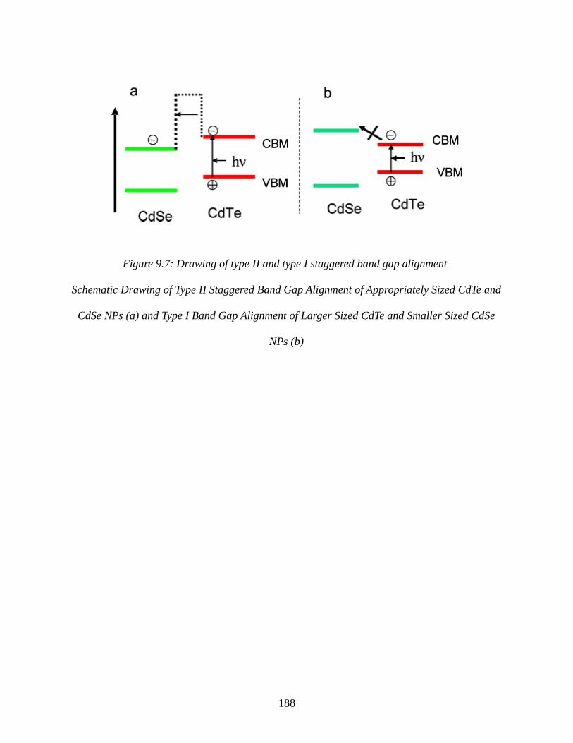
188
Figure 9.7: Drawing of type II and type I staggered band gap alignment
Schematic Drawing of Type II Staggered Band Gap Alignment of Appropriately Sized CdTe and
CdSe NPs (a) and Type I Band Gap Alignment of Larger Sized CdTe and Smaller Sized CdSe
NPs (b)
9.3.5 Surface Charge Dependence
The type II band alignment in Figure 9.7a implies that the electron transfer mechanism places an
extra negative charge on the CdSe NP and a consequent extra positive charge on the CdTe NP.
Given that the CdSe NP surface is positively charged and the CdTe NP surface is negatively
charged, the net charge separation between the two types of NPs is decreased by the electron
transfer. In contrast, one might expect that the transfer of an electron to a negatively charged
CdSe NP from a positively charged CdTe NP might be less facile because of the increase in
electrostatic energy, i.e., more net charge separation. This aspect of the electron transfer
quenching mechanism was explored by switching the capping ligands and thereby changing the
sign of the NP surface charges. DEA-CdTe NPs were synthesized by using a protocol similar to
that for the MPA-CdTe NP preparation, and the size was controlled in a similar manner.[19;
81] The first excitonic peak of the DEA-CdTe NPs occurs near 575 nm, and the
photoluminescence peak occurs near 610 nm. The MPA-CdSe NPs were prepared from the same
TOPO-CdSe NPs that have their first excitonic peak at 518 nm; upon ligand exchange with MPA
it shifted to 520 nm (see Figure 9.8).
189

190
Figure 9.8: Absorption and PL spectra of NPs used in surface charge dependence experiments
Representative absorption and photoluminescence spectra of DEA-CdTe and MPA-CdSe NPs
used in surface charge dependence experiments: from left to right, MPA-CdSe NP absorbance in
water (−−−), DEA-CdTe NP absorbance in water (---), and DEA-CdTe fluorescence in water
(—).
A solution of MPA-CdSe and DEA-CdTe at a molar ratio of 3:1 showed both excitonic
peaks of CdTe and CdSe NPs in absorption spectra but did not show a significant quenching
effect, as compared to a solution of DEA-CdTe (the PL spectrum of the assembly is similar and
not shown). DLS experiments gave aggregate sizes of several tens of nanometers, and ζ potential
measurements showed that the potential changed from about +14 mV for the original DEA-CdTe
to about −8 mV for MPA-CdSe/DEA-CdTe at a molar ratio of 3:1. Thus, the aggregation
properties are similar to those for the other aggregate type (negatively charged CdTe and
positively charged CdSe). The inefficient self-quenching of DEA-CdTe compared to the MPA-
CdTe systems may reflect the narrower size distribution of interaction energies (fwhm = 1652
cm−1for DEA-CdTe as opposed to 2038 cm−1 for MPA-CdTe; see the Supporting Information
[75]) as well as the shortening of the average fluorescence lifetime (14.1 ns for DEA-CdSe as
compared to 39.0 ns for MPA-CdTe). These findings show that the direction of the interparticle
electric field changes the photoluminescence quenching efficiency; a finding that is consistent
with charge transfer but not with energy transfer.
9.3.6 Kinetic Measurements
Time-resolved photoluminescence measurements, using the TCSPC method, were performed to
validate the steady-state measurements and quantify the relevant time scales for the quenching. A
diode laser at 440 nm and a dye laser at 585 nm were used as excitation sources, and the
emission was collected at the PL peak wavelength. None of the samples showed an excitation
wavelength dependence; therefore, only lifetime parameters from the 585 nm excitation are
presented here (Table 3 and Figure 9.9). Studies were performed for samples with molar ratios at
191
which the most pronounced difference in steady-state photoluminescence measurements were
observed. Table 3 summarizes the findings by presenting the parameters for a best fit of the data
to a sum of exponentials; the quantity τ is the average lifetime. ⟨ ⟩
The lifetime data corroborate the steady-state emission data. The photoluminescence
decay of the pure MPA-CdTe NP solution could be fit by a biexponential decay law with decay
times that are tens of nanoseconds, giving an average lifetime of 39.0 ns. This value is consistent
with typical thiol-capped CdTe NP emission lifetimes reported in the literature.[57; 76; 79]
Typically, the shorter lifetime is attributed to the intrinsic recombination of initially populated
core states, and the longer lifetime reflects the charge trapping kinetics of surface states via a
delayed fluorescence mechanism.[4; 8; 13; 29; 72; 73] The amplitude a2 of the
longer lifetime component accounts for nearly 80% of the total PL decay and indicates good
surface reconstruction with few recombination centers created during the sample growth process.
[72; 79] The TDA/MPA-CdTe and TMA-CdSe/MPA-CdTe NP solutions showed very
similar PL decay characteristics with an average lifetime of 24 ns. As discussed above these
solutions show steady-state emission quenching of about a factor of 2, and it is attributed to
aggregation-induced self-quenching of the CdTe NPs; the ratio of average lifetimes is consistent
with the steady-state PL measurement. The decay parameters show that both time constants
decrease but only by 10−20%. In contrast, the DEA-CdSe/MPA-CdTe solution showed a
dramatic lifetime shortening for both components with an average lifetime of 3.8 ns. This
observation is consistent with the steady-state studies and strongly suggests that interparticle
separation in the aggregates changes the relative importance of nonradiative decay pathways.
192

Lastly, a solution of MPA-CdSe/DEA-CdTe which inverts the NP surface charges, hence the sign
of the interparticle electric field, has an average lifetime similar to that of the pure solution of
DEA-CdTe. These data corroborate the steady-state measurements and their interpretation.
193

194
Figure 9.9: Time-Resolved PL decays of NP assemblies
(a) Representative time-resolved PL decays of MPA-CdTe, TMA-CdSe/MPA-CdTe at a 3:1 molar
ratio, and DEA-CdSe/MPA-CdTe at a 3:1 molar ratio in water. (b) Representative time-resolved
PL decays of MPA-CdTe, DEA-CdTe, and MPA-CdSe/DEA-CdTe at a 3:1 molar ratio in water.
The MPA-CdTe data were included in both panels for better comparison.
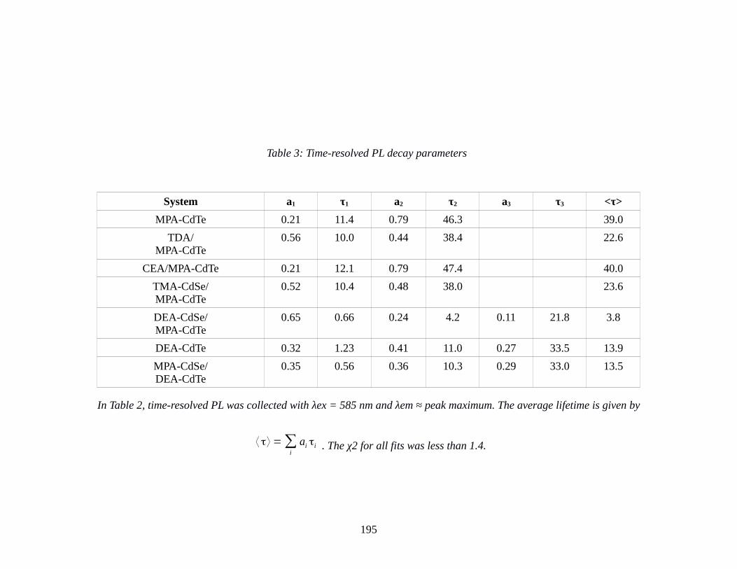
195
Table 3: Time-resolved PL decay parameters
System a1 τ1 a2 τ2 a3 τ3 <τ>
MPA-CdTe 0.21 11.4 0.79 46.3 39.0
TDA/MPA-CdTe
0.56 10.0 0.44 38.4 22.6
CEA/MPA-CdTe 0.21 12.1 0.79 47.4 40.0
TMA-CdSe/MPA-CdTe
0.52 10.4 0.48 38.0 23.6
DEA-CdSe/MPA-CdTe
0.65 0.66 0.24 4.2 0.11 21.8 3.8
DEA-CdTe 0.32 1.23 0.41 11.0 0.27 33.5 13.9
MPA-CdSe/DEA-CdTe
0.35 0.56 0.36 10.3 0.29 33.0 13.5
In Table 2, time-resolved PL was collected with λex = 585 nm and λem ≈ peak maximum. The average lifetime is given by
⟨ τ⟩ =∑i
ai τi . The χ2 for all fits was less than 1.4.
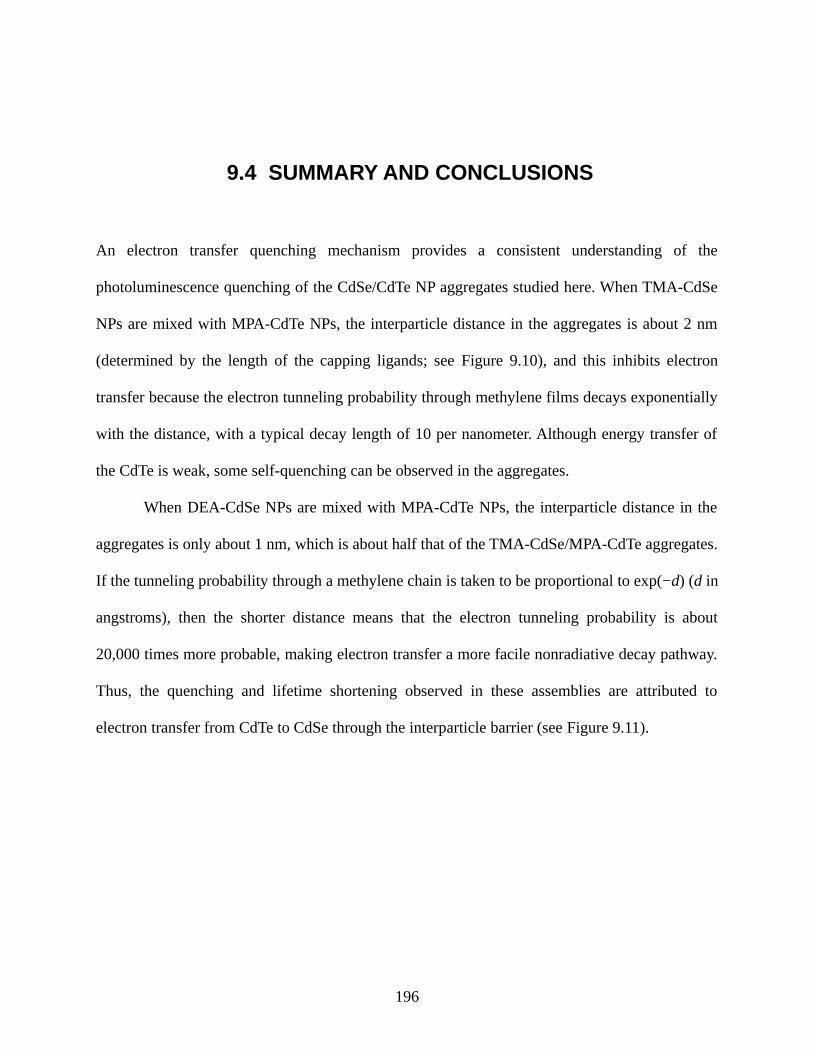
9.4 SUMMARY AND CONCLUSIONS
An electron transfer quenching mechanism provides a consistent understanding of the
photoluminescence quenching of the CdSe/CdTe NP aggregates studied here. When TMA-CdSe
NPs are mixed with MPA-CdTe NPs, the interparticle distance in the aggregates is about 2 nm
(determined by the length of the capping ligands; see Figure 9.10), and this inhibits electron
transfer because the electron tunneling probability through methylene films decays exponentially
with the distance, with a typical decay length of 10 per nanometer. Although energy transfer of
the CdTe is weak, some self-quenching can be observed in the aggregates.
When DEA-CdSe NPs are mixed with MPA-CdTe NPs, the interparticle distance in the
aggregates is only about 1 nm, which is about half that of the TMA-CdSe/MPA-CdTe aggregates.
If the tunneling probability through a methylene chain is taken to be proportional to exp(−d) (d in
angstroms), then the shorter distance means that the electron tunneling probability is about
20,000 times more probable, making electron transfer a more facile nonradiative decay pathway.
Thus, the quenching and lifetime shortening observed in these assemblies are attributed to
electron transfer from CdTe to CdSe through the interparticle barrier (see Figure 9.11).
196
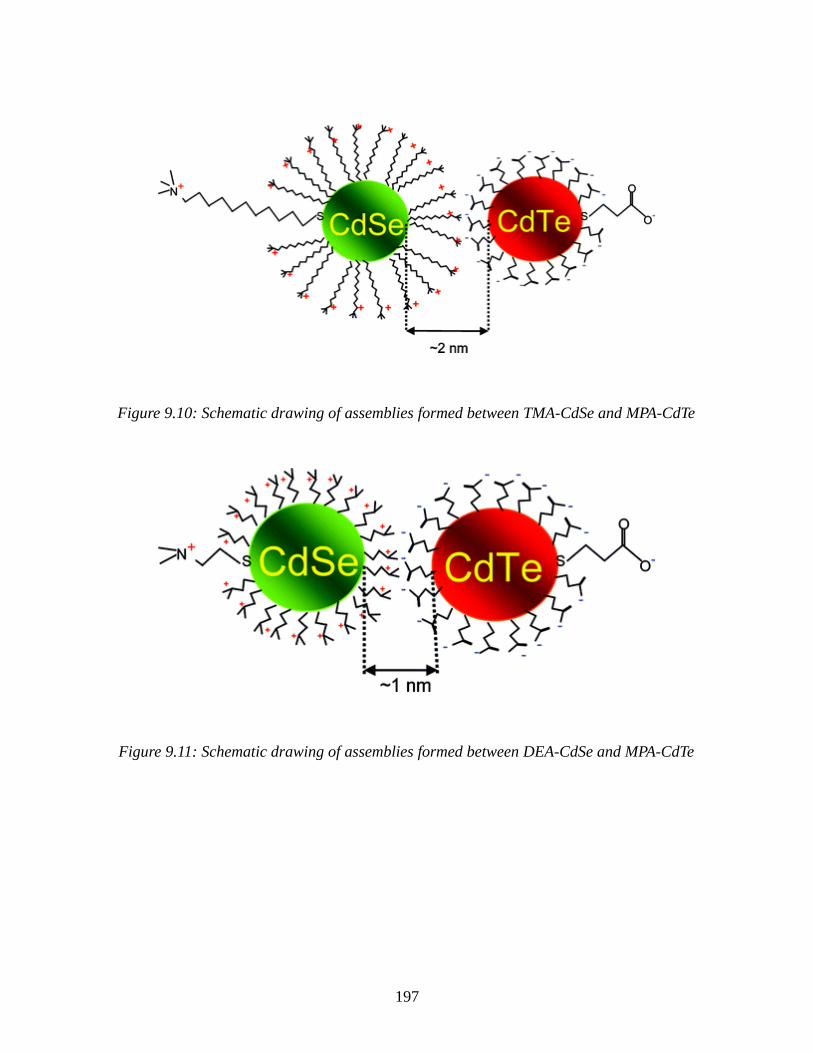
197
Figure 9.10: Schematic drawing of assemblies formed between TMA-CdSe and MPA-CdTe
Figure 9.11: Schematic drawing of assemblies formed between DEA-CdSe and MPA-CdTe
The assignment of the quenching mechanism to electron transfer was supported by
studies that inverted the surface charge on the NPs in the aggregates; in particular, CdTe was
capped with positively charged DEA, and CdSe was capped with negatively charged MPA. Thus,
the direction of the electric field between the two types of NPs was inverted (see Figure 9.12).
Although the optical properties and the aggregation properties of the NPs did not change
significantly with this change in surface ligand, the photoluminescence quenching of their
aggregates changed dramatically. Whether the change in rate with the field direction is caused by
a change in the tunneling probability and/or the relative energetics of the donor and accepting
states of the NPs is not yet known.
In conclusion, this study demonstrates that electron transfer and photoluminescence
quenching in CdSe/CdTe NP assemblies can be controlled through the interparticle distance,
energetics, electric field created by the surface capping group, and particle size. Time-resolved
studies indicate that the electron transfer process may involve surface-localized states. The
inhibition of electron transfer by the interparticle electric field is significant and may provide an
avenue for inhibiting back electron transfer. These findings should be useful for understanding
and controlling charge transfer in nanocrystal-based solar cells.
198
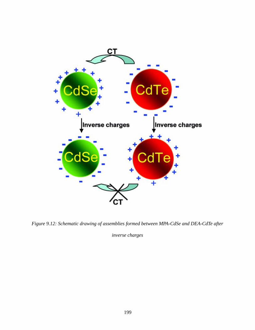
199
Figure 9.12: Schematic drawing of assemblies formed between MPA-CdSe and DEA-CdTe after
inverse charges

9.5 BIBLIOGRAPHY
[1] Akerman M., E.; Chan W. C., W.; Laakkonen, P.; Bhatia S., N. and Ruoslahti, E. (2002). , Proc. Natl. Acad. Sci. U.S.A. 99 : 12617.
[2] Aldana, J.; Wang Y., A. and Peng, X. (2001). , J. Am. Chem. Soc. 123 : 8844.
[3] Alivisatos A., P. (1996). , Science 271 : 933.
[4] Alivisatos A., P.; Harris A., L.; Levinos N., J.; Steigerwald M., L. and Brus L., E. (1988). , J. Chem. Phys. 89 : 4001.
[5] Andres R., P.; Bielefeld J., D.; Henderson J., I.; Janes D., B.; Kolagunta V., R.; Kubiak C., P.; Mahoney W., J. and Osifchin R., G. (1996). , Science 273 : 1690.
[6] Artemyev, M.; Woggon, U.; Wannemacher, R.; Jaschinski, H. and Langbein, W. (2001). , Nano Lett. 1 : 309.
[7] Barnham K. W., J.; Mazzer, M. and Clive, B. (2006). , Nat. Mater. 5 : 161.
[8] Bawendi M., G.; Carroll P., J.; Wilson W., L. and Brus L., E. (1992). , J. Chem. Phys. 96 : 946.
[9] Bethell D. B., M.; Schiffrin D., J. and Kiely, C. (1996). , J. Electroanal. Chem. 409 : 137.
[10] Bruchez, M.; Moronne, M.; Gin, P.; Weiss, S. and Alivisatos P., A. (1998). , Science 281 : 2013.
[11] Brus L., E. (1986). , J. Chem. Phys. 90 : 2555.
[12] Brust, M.; Schiffrin D., J.; Bethell, D. and Kiely C., J. (1995). , Adv. Mater. 7 : 795.
[13] Byrne S., J.; Corr S., A.; Rakovich T., Y.; Gun’ko Y., K.; Rakovich Y., P.; Donegan J., F.; Mitchell, S. and Volkov, Y. (2006). , J. Mater. Chem. 16 : 2896.
[14] Chan W. C., W. and Nie, S. (1998). , Science 281 : 2016.
[15] Crooker S., A.; Hollingsworth J., A.; Tretiak, S. and Klimov V., I. (2002). , Phys. Rev. Lett. 89 : 186802/1.
[16] Dimitrijevic N., M.; Saponjic Z., V.; Rabatic B., M. and Rajh, T. (2005). , J. Am. Chem. Soc. 127 : 1344.
200

[17] Dooley C., J.; Dimitrov S., D. and Fiebig, T. (2008). , J. Phys. Chem. C 112 : 12074.
[18] Ellingson R., J.; Beard M., C.; Johnson J., C.; Yu, P.; Micic O., I.; Nozik A., J.; Shabaev, A. and Efros A., L. (2005). , Nano Lett. 5 : 865.
[19] Gaponik, N.; Talapin D., V.; Rogach A., L.; Hoppe, K.; Shevchenko E., V.; Kornowski, A.; Eychmu1ller, A. and Weller, H. (2002). , J. Phys. Chem. B 106 : 7177.
[20] Goldman E., R.; Clapp A., R.; Anderson G., P.; Uyeda H., T.; Mauro J., M.; Medintz I., L. and Mattoussi, H. (2004). , Anal. Chem. 76 : 684.
[21] Gopidas K., R.; Bohorquez, M. and Kamat P., V. (1990). , J. Phys. Chem. 94 : 6435.
[22] Green M., A.; Emery, K.; King D., L.; Igari, S. and Warta, W. (2001). , Prog. Photovoltaics 9 : 287.
[23] Gross, D.; Susha A., S.; Klar T., A.; Como E., D.; Rogach A., L. and Feldmann, J. (2008). , Nano Lett. 8 : 1482.
[24] Heath J., R.; Knobler C., M. and Leff D., V. (1997). , J. Phys. Chem. B 101 : 189.
[25] Huynh W., U.; Dittmer J., K. and Alivisatos A., P. (2002). , Science 295 : 2425.
[26] Issac, A.; Jin, S. and Lian, T. (2008). , J. Am. Chem. Soc. 130 : 11280.
[27] J.-W., H. and Bai S., J. (2005). , Nanotechnology 16 : 1406.
[28] Jin W., J.; Fernandez-Arguelles M., T.; Costa-Fernandez J., M.; Pereiro, R. and Sanz-Medel, A. (2005). , Chem. Commun. : 883.
[29] Jones, M.; Lo S., S. and Scholes G., D. (2009). , Proc. Natl. Acad. Sci. U.S.A. 106 : 3011.
[30] Kagan C., R.; Murray C., B.; Nirmal, M. and Bawendi M., G. (1996). , Phys. Rev. Lett. 76 : 1517.
[31] Kalsin A., M.; Fialkowski, M.; Paszewski, M.; Smoukov S., K.; Bishop K. J., M. and Grzybowski B., A. (2006). , Science 312 : 420.
[32] Kamat P., V. (2002). , J. Phys. Chem. B 106 : 7729.
[33] Kamat P., V. (2007). , J. Phys. Chem. C 111 : 2834.
[34] Kim, S.; Fisher, B.; H.-J., E. and Bawendi, M. (2003). , J. Am. Chem. Soc. 125 : 11466.
[35] Klimov V., I.; Mikhailovsky A., A.; Xu, S.; Malko, A.; Hollingsworth J., A.; Leatherdale C., A.; Eisler H., J. and Bawendi M., G. (2000). , Science 290 : 314.
[36] Kohtani, S.; Kudo, A. and Sakata, T. (1993). , Chem. Phys. Lett. 206 : 166.
201

[37] Koole, R.; Liljeroth, P.; De Mello Donega, C.; Vanmaekelbergh, D. and Meijerink, A. (2006). , J. Am. Chem. Soc. 128 : 10436.
[38] Leibowitz F., L.; Zheng, W.; Maye M., M. and Zhong C., J. (1999). , Anal. Chem. 71 : 5076.
[39] Liu, M.; Kaur, P.; Waldeck D., H.; Xue, C. and Liu, H. (2005). , Langmuir 21 : 1687.
[40] Liu, M.; Waldeck D., H.; Oliver A., M.; Head N., J. and Paddon-Row M., N. (2004). , J. Am. Chem. Soc. 126 : 10778.
[41] Liu, Y.; Wang, Y. and Claus R., O. (1998). , Chem. Phys. Lett. 298 : 315.
[42] Lo S., S.; Khan, Y.; Jones, M. and Scholes G., D. (2009). , J. Chem. Phys. 131 : 084714.
[43] Mahawela, P.; Jeedigunta, S.; Vakkalanka, S.; Ferekides C., S. and Morel D., L. (2005). , Thin Solid Films 466 : 480.
[44] Maheshwari, V. and Saraf R., F. (2006). , Science 312 : 1501.
[45] Mayilo, S.; Hilhorst, J.; Susha A., S.; Hohl, C.; Franzl, T.; Klar T., A.; Rogach A., L. and Feldmann, J. (2008). , J. Phys. Chem. C 112 : 14589.
[46] McFarland E., W. and Tang, J. (2003). , Nature 421 : 616.
[47] Mews, A.; Kadavanich A., V.; Banin, U. and Alivisatos A., P. (1996). , Phys. Rev. B 53 : 13242.
[48] Michalet, X.; Pinaud F., F.; Bentolila L., A.; Tsay J., M.; Doose, S.; Li J., J.; Sundaresan, G.; Wu A., M.; Gambhir S., S. and Weiss, S. (2005). , Science 307 : 538.
[49] Murray C., B.; Kagan C., R. and Bawendi M., G. (2000). , Annu. Rev. Mater. Sci. 30 : 545.
[50] Nasr, C.; Hotchandani, S.; Kim W., Y.; Schmehl R., H. and Kamat P., V. (1997). , J. Phys. Chem. B 101 : 7480.
[51] Park S., H.; Roy, A.; Beaupré, S.; Cho, S.; Coates, N.; Moon J., S.; Moses, D.; Leclerc, M.; Lee, K. and Heeger A., J. (2009). , Nat. Photon 3 : 297.
[52] Pathak, S.; Choi S., K.; Arnheim, N. and Thompson M., E. (2001). , J. Am. Chem. Soc. 123 : 4103.
[53] Peng Z., A. and Peng, X. (2001). , J. Am. Chem. Soc. 123 : 183.
[54] Plass, R.; Pelet, S.; Krueger, J.; Gratzel, M. and Bach, U. (2002). , J. Phys. Chem. B 106 : 7578.
[55] Qu, L.; Peng Z., A. and Peng, X. (2001). , Nano Lett. 1 : 333.
202

[56] Robel, I.; Subramanian, V.; Kuno, M. and Kamat P., V. (2006). , J. Am. Chem. Soc. 128 : 2385.
[57] Rogach A., L.; Franzl, T.; Klar T., A.; Feldmann, J.; Gaponik, N.; Lesnyak, V.; Shavel, A.; Eychmuller, A.; Rakovich Y., P. and Donegan J., F. (2007). , J. Phys. Chem. C 111 : 14628.
[58] S.-C., C.; Tachikawa, T.; Fujitsuka, M. and Majima, T. (2008). , J. Phys. Chem. C 112 : 19625.
[59] Sapsford K., E.; Medintz I., L.; Golden J., P.; Deschamps J., R.; Uyeda H., T. and Mattoussi, H. (2004). , Langmuir 20 : 7720.
[60] Schaller R., D.; Sykora, M.; Pietryga J., M. and Klimov V., I. (2006). , Nano Lett. 6 : 424.
[61] Scharber M., C.; Muhlbacher, D.; Koppe, M.; Denk, P.; Waldauf, C.; Heeger A., J. and Brabec C., J. (2006). , Adv. Mater. 18 : 789.
[62] Schlamp M., C.; Peng X., G. and Alivisatos A., P. (1997). , J. Appl. Phys. 82 : 5837.
[63] Skolnick M., S. and Mowbray D., J. (2004). , Annu. Rev. Mater. Res. 34 : 181.
[64] Sudeep P., K.; Takechi, K. and Kamat P., V. (2007). , J. Phys. Chem. C 111 : 488.
[65] Sundar V., C.; Lee, J.; Heine J., R.; Bawendi M., G. and Jensen K., F. (2000). , Adv. Mater. 12 : 1102.
[66] Talapin D., V. and Murray C., B. (2005). , Science 310 : 86.
[67] Tang, Z.; Zhang, Z.; Wang, Y.; Glotzer S., C. and Kotov N., A. (2006). , Science 314 : 274.
[68] Uyeda H., T.; Medintz I., L.; Jaiswal J., K.; Simon S., M. and Mattoussi, H. (2005). , J. Am. Chem. Soc. 127 : 3870.
[69] Vanmaekelbergh, D.I. and Liljeroth, P. (2005). , Chem. Soc. Rev. 34 : 299.
[70] Vinodgopal, K.; Bedja, I. and Kamat P., V. (1996). , Chem. Mater. 8 : 2180.
[71] Wang, L.; Rastelli, A.; Kiravittaya, S.; Benyoucef, M. and Schmidt O., G. (2009). , Adv. Mater. 21 : 2601.
[72] Wang, X.; Qu, L.; Zhang, J.; Peng, X. and Xiao, M. (2003). , Nano Lett. 3 : 1103.
[73] Wehrenberg B., L.; Wang, C. and Guyot-Sionnest P., J. (2002). , J. Phys. Chem. B 106 : 10634.
[74] Willner, I. and Eichen, Y. (1987). , J. Am. Chem. Soc. 109 : 6862.
203

[75] Wu, M.; Mukherjee, P.; Lamont, D. N. and Waldeck, D. H. (2010). Electron Transfer and Fluorescence Quenching of Nanoparticle Assemblies, The Journal of Physical Chemistry C 114 : 5751-5759.
[76] Wuister S., F.; Swart, I.; Van Driel, F.; Hickey S., G. and De Mello Donega, C. (2003). , Nano Lett. 3 : 503.
[77] Yu, G.; Gao, J.; Hemmelen J., C.; Wudl, F. and Heeger A., J. (1995). , Science 270 : 1789.
[78] Zabet-Khosousi, A. and A.-A., D. (2008). , Chem. Rev. 108 : 4072.
[79] Zhao, K.; Li, J.; Wang, H.; Zhuang, J. and Yang, W. (2007). , J. Phys. Chem. C 111 : 5618.
[80] Zhou, Q.; Li, X.; Fan, Q.; Zhang, X. and Zheng, J. (2006). , Angew. Chem., Int. Ed. 45 : 3970.
[81] Zou, L.; Gu, Z.; Zhang, N.; Zhang, Y.; Fang, Z.; Zhu, W. and Zhong, X. (2008). , J. Mater. Chem. 18 : 2807.
204
10.0 LANTHANIDE SENSITIZATION IN II−VI
SEMICONDUCTOR MATERIALS: A CASE STUDY
WITH TERBIUM(III) AND EUROPIUM(III) IN ZINC
SULFIDE NANOPARTICLES
Author list: Prasun Mukherjee, Chad M. Shade, Adrienne M. Yingling, Daniel N. Lamont,
David H. Waldeck, and Stéphane Petoud
Author contribution: The author of this dissertation contributed to the photophysical
characterization of the nanoparticles, interpretation of the results and the preparation of the
manuscript. This work has been published as J. Phys. Chem. A 2011 115, 4031
10.1 INTRODUCTION
Historically, luminescent lanthanides have been extensively used as phosphors, and more
recently, they have attracted interest as a new class of luminescent probes and sensors for
biological applications.[5; 9; 35; 49; 50; 61; 74] Lanthanides have a number of
luminescence properties that make them an attractive alternative to organic fluorophores in
205
bioanalytical applications and biological imaging. Whereas typical organic fluorophores are
prone to photobleaching mechanisms, lanthanide luminescence is highly resistant to
photobleaching and, hence, allows longer experiment times or their repetition. The sharp atom
like lanthanide emission bands and the negligible overlap between the bands of different
lanthanide ions makes them promising candidates for multiplex biological assays through
spectral discrimination or for barcode types of applications.[81] Moreover, the long lanthanide
luminescence lifetimes (millisecond time range for lanthanide emitting in the visible) allows
their signal to be distinguished from the background autofluorescence of biological media
(nanosecond time range) through temporal discrimination for improved detection sensitivity.
A major requirement for the use of lanthanides as biological imaging agents is the
detection sensitivity they can provide, which includes the emission of a sufficient number of
photons to obtain good detection sensitivity. The direct excitation of lanthanides is inefficient
because most of the interesting f−f transitions are Laporte-forbidden.[10; 29] As a
consequence, the molar extinction coefficients of lanthanide ions are very low[11] (≤10 M−1
cm−1, as opposed to 104−105 M−1 cm−1 for typical organic fluorophores). The low number of
absorbed photons will result in a low number of emitted photons. To overcome this limitation,
the concept of sensitization through an antenna effect has been established.[2; 4; 7; 17;
41; 42; 50; 53; 63; 64; 83; 84] In this process, photons from the excitation light
are absorbed by a chromophore with high extinction coefficient that transfers the energy to the
accepting levels of the lanthanide ions, thus creating a high population of electronically excited
lanthanide ions and enhancing the amount of luminescent photons. In addition to efficient energy
pumping by this antenna effect, it is also important to prevent the quenching of lanthanide ion
206
excited states by nonradiative energy transfer to the overtones of high frequency vibrational
modes, such as −OH, −NH, and −CH.[3] For applications under biological conditions, it is
especially important to protect the lanthanide ions from water molecules.
Semiconductor nanoparticles that contain lanthanide ions are advantageous for biological
applications over the undoped nanoparticles because the sharp emission signal corresponding to
each lanthanide ion has a unique spectroscopic signature for spectral identification and
unambiguous identification. Depending on the lanthanide cations, there is a broad choice of
emission wavelength throughout the entire visible and near-IR spectral regions. The near-IR
luminescence of lanthanide cations is of special benefit for biological applications because (i)
there is an absence of native autofluorescence of tissues in the near−IR region; therefore, a good
signal-to-noise ratio is obtained for more sensitive detection, and (ii) near-IR photons can cross
significant depths of tissues for potential noninvasive investigation.
Recently, Chengelis et al. reported on the incorporation of terbium ions (Tb3+) in CdSe
nanoparticles.[19] Although Tb3+ luminescence sensitization was observed for the CdSe/Tb3+
system, its emission was obscured by the more intense CdSe bandgap emission in steady-state
mode, and a time-gated method was required to specifically identify the Tb3+ luminescence.
From the excitation spectrum, collected upon monitoring the 545 nm centered Tb3+ emission
signal, it is evident that part of the excitation energy is transferred from the CdSe nanoparticle
states to the accepting energy levels of Tb3+ ions, demonstrating that the electronic structure of
the nanoparticle can act as an antenna.
207
Although the CdSe/Tb3+ system demonstrates the use of the nanoparticles as an antenna,
it has intrinsic limitations; namely, the efficiency of CdSe in sensitizing Tb3+ luminescence was
low, and the Cd and Se components of the nanoparticles are toxic, thus limiting their
applicability for studying biological systems and for diagnostic purposes. To overcome these two
drawbacks, we have created a ZnS/Tb3+ nanoparticle system, in which the individual
constituents are nontoxic or less toxic and more environmentally friendly. Moreover, because the
bulk band gap of ZnS is larger than that of CdSe (3.6 eV as opposed to 1.7 eV),[66] the
electronic structure of ZnS is expected to sensitize lanthanides more efficiently than CdSe
because it ensures a more favorable match of lanthanide acceptor energy levels with respect to
the nanoparticle donating energy levels.[27]
This work reports results on ZnS nanoparticles containing three different lanthanides: two
visible-emitting lanthanides, Tb3+ and Eu3+ in ZnS nanoparticles, and corresponding control
experiments with Gd3+ (which does not have accepting electronic levels in the relevant energy
range). ZnS nanoparticle systems without lanthanides were also studied for comparison. Both
steady-state and time-resolved luminescence measurements demonstrate that ZnS acts as an
efficient antenna to sensitize Tb3+ and Eu3+ luminescence. A comparison with other II−VI
materials (namely, Tb3+ incorporated in CdSe, CdS, and ZnSe) is made to elucidate the energy
transfer mechanism between the lanthanide and the nanoparticle host.
Understanding the mechanism of lanthanide luminescence sensitization is of main
importance for controlling the performance and properties of novel optical materials. Because
lanthanide ions behave as hard acids, they bind strongly to hard bases, following the preference
order O > N > S. Various researchers have devoted considerable effort to understanding and
208
exploiting the mechanisms for the luminescence sensitization of lanthanide ions in
semiconductor materials. Some of the discussed mechanisms are based on a defect-related Auger
transition model,[1; 31; 86] a resonant energy transfer model,[44] bound exciton models,
[53; 79] and shallow donor (or acceptor) models.[34] It is generally believed that exciton
recombination plays a key role in the luminescence sensitization of lanthanide cations.
Although a number of researchers have discussed lanthanide luminescence in bulk
semiconductors[18; 32; 33; 39; 43; 58; 59; 69-72] and semiconductor
nanoparticles,[6; 13; 14; 21; 28; 36; 37; 57; 60; 67; 68; 80; 85] the
mechanism of lanthanide luminescence sensitization is still not fully elucidated and does not
allow the synthesis of lanthanide-based nanomaterials with predictable properties. The
mechanism of Tb3+ luminescence sensitization in bulk ZnS has attracted considerable attention.
For example, Anderson[2] finds that the process includes (a) a donor level related to Tb3+
[6s25d1] that lies 0.4 eV below the conduction band (the 4f8 levels were assumed to be located
somewhere below the valence band), (b) a hole trap that lies 1.02 eV above the valence band
(assumed to be a copper-related site),[40; 47] and (c) that the excitation of the 4f8 electronic
system occurs during recombination of the electron−hole pair in these traps. Although these
efforts provide a useful framework for the current studies, the luminescence sensitization of Tb3+
and Eu3+ in ZnS nanoparticles is not well understood. Previous studies have been limited by an
inability to identify the location of lanthanide ground and excited states with respect to the
valence and conduction bands of the semiconductor materials. In this work, the nature of
sensitization in the ZnS nanoparticles is discussed in light of the model proposed by Dorenbos,
[22-27] for the relative energetics of the lanthanide ions in the host semiconductor.
209
10.2 MATERIALS AND METHODS
10.2.1 Chemicals
Trioctylphosphine [TOP] (90%), zinc stearate (tech.), octadecene (90% tech.), and tetracosane
(99%) were purchased from Sigma-Aldrich-Fluka, St. Louis, MO. Chloroform was purchased
from J. T. Baker, Phillipsburg, NJ. Sulfur, toluene, and methanol were purchased from Fisher
Scientific, Pittsburgh, PA. Terbium(III) nitrate (99.9%) was purchased from Strem, europium(III)
nitrate (99.99%) was purchased from Aldrich, and gadolinium(III) nitrate (99.99%) was
purchased from Alfa Aesar, Ward Hill, MA. In all cases, hydrated lanthanide salts were used. n-
Hexane and 1-octanol were purchased from Acros, and ethyl acetate was purchased from EMD,
Gibbstown, NJ. Argon gas was purchased from Valley National, Pittsburgh, PA. All chemicals
were used as purchased without purification, except toluene, which was distilled over sodium
under nitrogen.
10.2.2 Nanoparticle Synthesis
All ZnS nanoparticle systems were synthesized using a noncoordinating solvent system
consisting of octadecene and tetracosane. Zinc stearate and lanthanide nitrate salts were used as
cation precursors, and elemental sulfur served as the anion precursor. Tetracosane (4.0 g),
octadecene (3.0 mL), and 0.68 mmol of zinc stearate were loaded into a three-neck, round-
bottom flask and heated to 350 °C while stirring under nitrogen. The lanthanide stock solution
210
(0.12 mmol lanthanide nitrate dissolved in a combination of octadecene and trioctylphosphine
oxide) was injected after approximately 2 h of heating and allowed to stir within the reaction∼
mixture for at least 30 min. The sulfur stock solution (sulfur powder dissolved in octadecene)
was injected 1 h after the lanthanide stock solution. The reaction temperature was then∼
decreased to between 270 and 300 °C for the duration of nanocrystal growth. Aliquots of sample
were removed at varying growth times. The resulting nanoparticles were then redispersed in an
appropriate solvent for spectroscopic analysis.
ZnS nanoparticles without lanthanides incorporated were prepared using the methods
described above; however, the zinc stearate precursor was increased to 0.80 mmol, and the
lanthanide stock solution preparation was omitted.
10.2.3 Steady-State Optical Measurements
Steady-state absorption spectra were obtained on an Agilent 8453 UV−visible spectrophotometer
with 1 nm resolution. Steady-state excitation and emission spectra were recorded using a Jobin
Yvon Horiba Fluorolog-322 with a 5 nm bandpass; spectra were corrected for excitation and
emission (lamp, detector, and monochromator). A 1 cm path length quartz cuvette was used for
the measurements. All measurements were performed at room temperature.
10.2.4 Quantum Yields
Absorption spectra were recorded on either a Perkin-Elmer Lambda 9 Spectrometer coupled to a
personal computer using software supplied by Perkin-Elmer or on an Agilent 8453 UV−visible
spectrophotometer. Quantum yields were recorded by the relative method using references.
211

Steady-state luminescence quantum yields were measured using quinine sulfate reference
solution (solvent H2SO4 1 N, Φ = 0.546).[48] Time-gated luminescence quantum yields were
measured using [Tb(H22IAM)] reference solution (solvent water, Φ = 0.59).[55] Spectra were
corrected for the instrumental response.
The quantum yields were calculated using the following Equation 10.1:
where the subscript r stands for the reference, and x, for the sample; A is the absorbance at the
excitation wavelength, I is the intensity of the excitation light at the same wavelength, η is the
refractive index (η = 1.333 in water, η = 1.496 in toluene, η = 1.446 in chloroform), and D is the
measured integrated luminescence intensity. ZnS systems (λex = 315, 320, and 325 nm) were
measured in chloroform, whereas ZnSe (λex = 315, 320, and 325 nm) and CdSe (λex = 300, 305,
and 310 nm) systems were measured in toluene.
Lanthanide-centered quantum yields for ZnSe/Ln3+ and CdSe/Ln3+ were collected with
the fluorometer in time-gated mode, whereas the contribution from lanthanide-centered emission
was discriminated spectrally from the overall quantum yield. For the ZnS/Ln3+ systems,
calculations were performed by integrating the narrow emission bands arising from the
lanthanide cations in steady-state mode.
212
Φx
Φr=
Ar (λr)I (λ r)ηx2 D x
A x (λx ) I (λx)ηr2 Dr
Equation 10.1
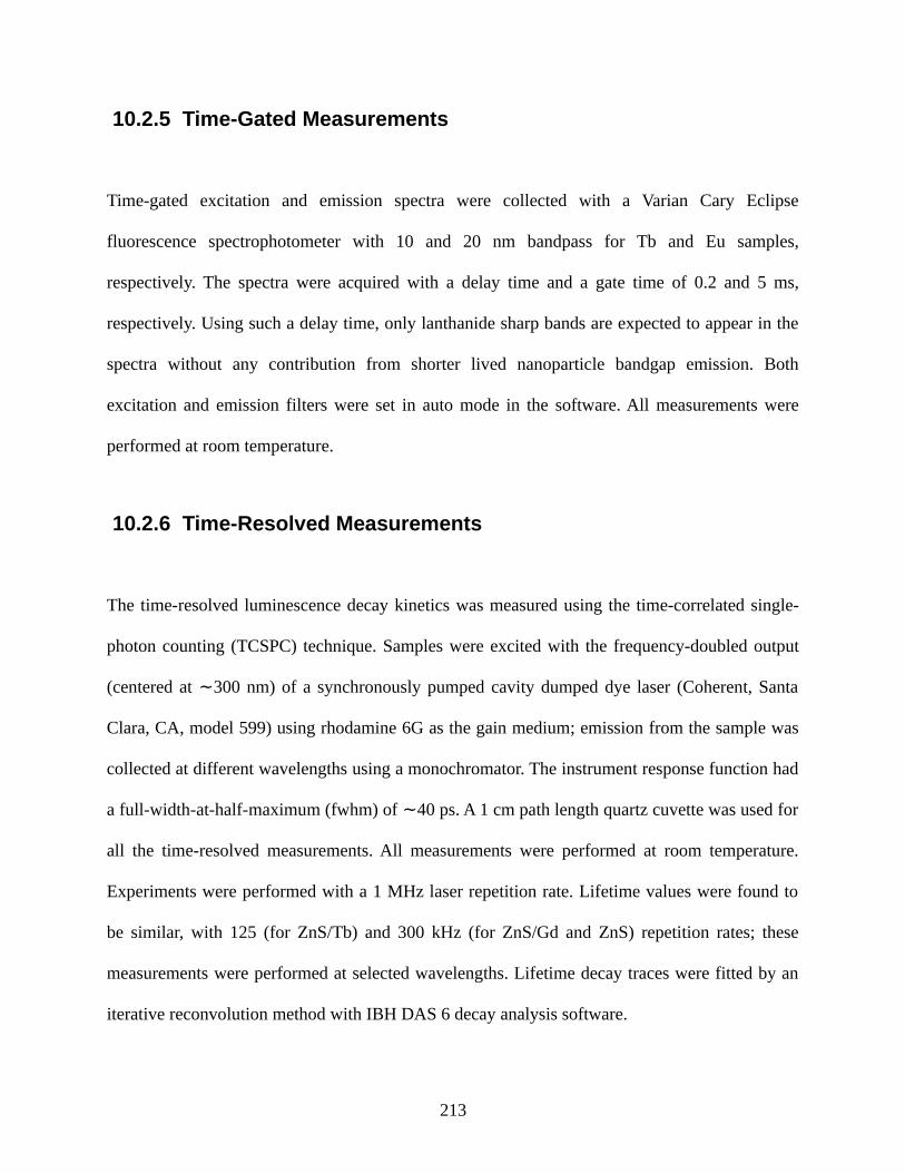
10.2.5 Time-Gated Measurements
Time-gated excitation and emission spectra were collected with a Varian Cary Eclipse
fluorescence spectrophotometer with 10 and 20 nm bandpass for Tb and Eu samples,
respectively. The spectra were acquired with a delay time and a gate time of 0.2 and 5 ms,
respectively. Using such a delay time, only lanthanide sharp bands are expected to appear in the
spectra without any contribution from shorter lived nanoparticle bandgap emission. Both
excitation and emission filters were set in auto mode in the software. All measurements were
performed at room temperature.
10.2.6 Time-Resolved Measurements
The time-resolved luminescence decay kinetics was measured using the time-correlated single-
photon counting (TCSPC) technique. Samples were excited with the frequency-doubled output
(centered at 300 nm) of a synchronously pumped cavity dumped dye laser (Coherent, Santa∼
Clara, CA, model 599) using rhodamine 6G as the gain medium; emission from the sample was
collected at different wavelengths using a monochromator. The instrument response function had
a full-width-at-half-maximum (fwhm) of 40 ps. A 1 cm path length quartz cuvette was used for∼
all the time-resolved measurements. All measurements were performed at room temperature.
Experiments were performed with a 1 MHz laser repetition rate. Lifetime values were found to
be similar, with 125 (for ZnS/Tb) and 300 kHz (for ZnS/Gd and ZnS) repetition rates; these
measurements were performed at selected wavelengths. Lifetime decay traces were fitted by an
iterative reconvolution method with IBH DAS 6 decay analysis software.
213
The Tb3+ and Eu3+ luminescence lifetime measurements were performed by excitation of
solutions in 1 mm quartz cells (NSG Precision Cells, Inc., Farmingdale, NY) using either a
Xenon flash lamp or a Nd:YAG Continuum Powerlite 8100 laser (354 nm, third harmonic) as the
excitation source. Emission was collected at a right angle to the excitation beam, and
wavelengths were selected by means of the Spex FL1005 double monochromator or a Spectral
Products CM 110 1/8 m monochromator. The signal was monitored by a Hamamatsu R928
photomultiplier tube coupled to a 500 MHz bandpass digital oscilloscope (Tektronix TDS 620B).
Signals from >500 flashes were collected and averaged. Luminescence lifetimes were averaged
using samples from several different batches. Luminescence decay curves were imported into
Origin 7.0 and analyzed using the Advanced Fitting Tool.
10.3 RESULTS AND DISCUSSION
10.3.1 HRTEM Imaging
High-resolution transmission electron microscopy (HRTEM) images were obtained using a
JEOL-2100 CF instrument operating between 120 kV and 200 kV. A representative TEM image
is shown in Figure 10.1. The size distribution of ZnS:Tb nanoparticles was calculated using
Image J software and found to be 3.3 ± 0.4 nm in average diameter. Both the stoichiometry
(lanthanide-to-zinc ratio) and the location of the lanthanides in the nanoparticles are not yet fully
214

quantified. These data will be reported in a more comprehensive future study that will address
the stoichiometry and the relative importance of the lanthanide locations, on the surface or in the
bulk of the nanoparticles.
215
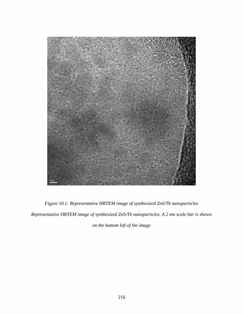
216
Figure 10.1: Representative HRTEM image of synthesized ZnS/Tb nanoparticles
Representative HRTEM image of synthesized ZnS/Tb nanoparticles. A 2 nm scale bar is shown
on the bottom left of the image
10.3.2 Absorption Spectra
Representative absorption spectra of ZnS nanoparticles dissolved in chloroform are shown in
Figure 10.2 for two different growth times. The absorption spectra reveal characteristic bands
centered at 290 and 360 nm. The band with an apparent maximum at 290 nm shows a∼ ∼ ∼
small dependence on growth time and is attributed to the lowest energy exciton band of the
nanoparticle. The 360 nm band is probably associated with a transition involving a trap state.∼
The assignment of the 290 nm band is corroborated by a simple estimation of the nanoparticle∼
band gap using a method proposed by Brus [8] (Equation 10.2), and found to be 4.2 eV,∼
corresponding to a 290 nm band gap transition. In this model, the change in bandgap with∼
nanoparticle size is given by
assuming Eg(bulk) = 3.6 eV, R = 1.65 nm (see above), me = 0.25 m0, mh = 0.59 m0 and ε = 8.3.
The effective mass and dielectric constant values were adopted from the work by Murphy and
co-workers.[65] We assign the long wavelength tail to the contribution from various surface
states of the nanoparticles (vide infra).
217
Eg(nano)≈ Eg(bulk)+ℏ
2π
2
2R2 [ 1me
+1
mh ]−1.8 e2
ϵR
Equation 10.2
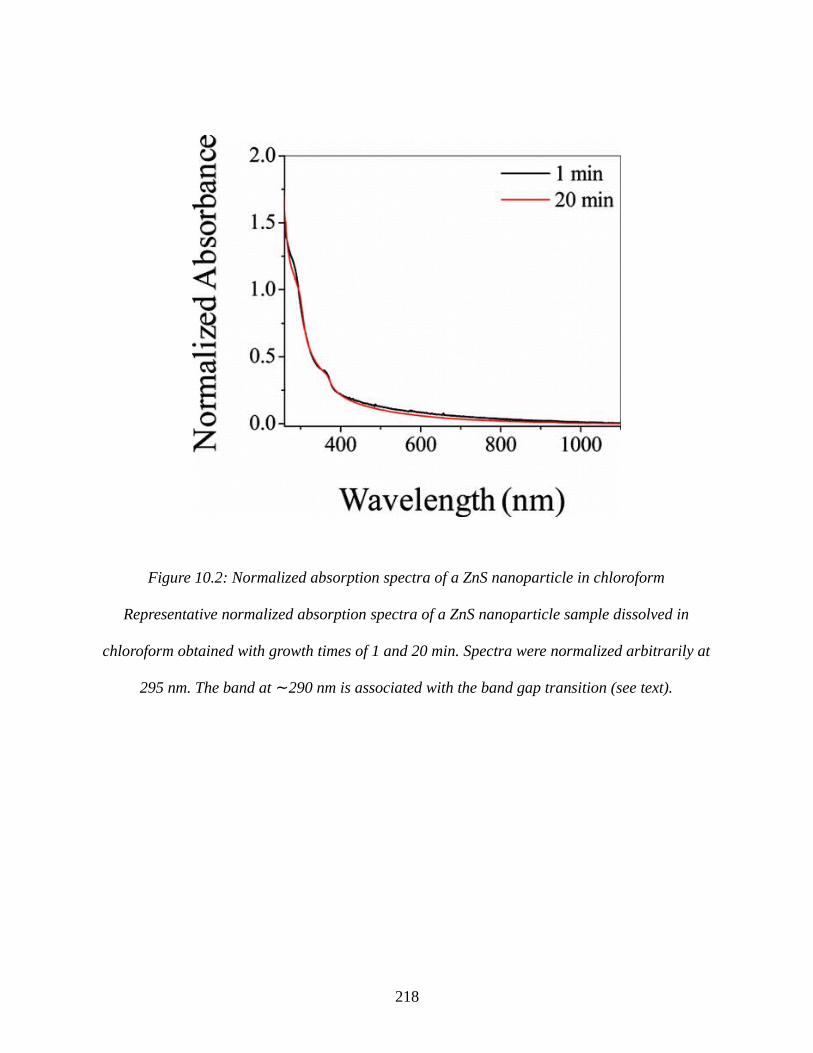
218
Figure 10.2: Normalized absorption spectra of a ZnS nanoparticle in chloroform
Representative normalized absorption spectra of a ZnS nanoparticle sample dissolved in
chloroform obtained with growth times of 1 and 20 min. Spectra were normalized arbitrarily at
295 nm. The band at 290 nm is associated with the band gap transition (see text).∼

Figure 10.3 shows steady-state luminescence excitation and emission spectra for the
lanthanide incorporated ZnS nanoparticles and for undoped ZnS nanoparticles (NP) without
lanthanide ions, in CHCl3. The spectra correspond to 20 min NP growth time; the spectra∼
corresponding to the analysis of the samples obtained after 1 min growth times are similar.
10.3.3 ZnS/Tb Spectra
Figure 10.3B shows emission spectra for ZnS/Tb. For λex = 300 nm, λem bands were identified at
410 (ZnS band), 490, 545, 585, and 620 nm (Tb∼ 3+ sharp bands); for λex = 375 nm, λem bands
were assigned at 455 (ZnS band), 490 (weak Tb∼ 3+ band), and 545 nm (Tb3+ band); and for λex
= 440 nm, a λem band was assigned at 510 nm (ZnS band). An excitation wavelength∼
dependence (red edge effect) is observed, that is, with an increase in λex, the emission band
position shifts toward the red.
The excitation spectra (Figure 10.3A) also depend on λem. For λem = 410 nm (ZnS
emission), the λex bands were identified at 260 and 350 nm; for λ∼ em = 450 nm (ZnS emission),
the λex bands were assigned at 270 and 375 nm; and for λ∼ em = 545 nm (Tb3+ emission), a broad
λex feature appeared. To examine whether this wavelength dependence reflects size heterogeneity
of the sample, efforts were made to improve the sample’s size distribution. Thus, centrifugation
was performed at 20 000 rpm for 2 h, a chemical purification by solvent precipitation method
(see Supporting Information [51] ) was used, and the nanoparticle samples were dialyzed.
None of these three methods yielded any noticeable change in the excitation wavelength-
dependent behavior. On the basis of these studies, the excitation wavelength-dependent emission
spectra are taken to reflect the energy distribution of surface states on the nanoparticles.
219
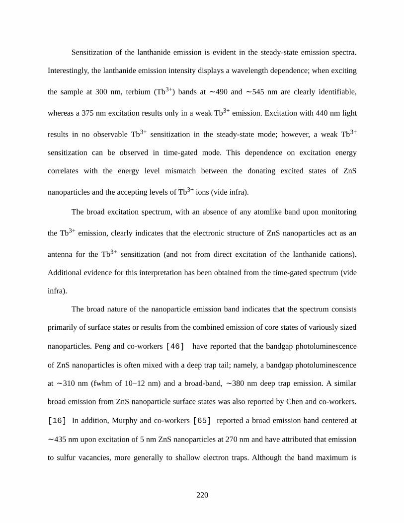
Sensitization of the lanthanide emission is evident in the steady-state emission spectra.
Interestingly, the lanthanide emission intensity displays a wavelength dependence; when exciting
the sample at 300 nm, terbium (Tb3+) bands at 490 and 545 nm are clearly identifiable,∼ ∼
whereas a 375 nm excitation results only in a weak Tb3+ emission. Excitation with 440 nm light
results in no observable Tb3+ sensitization in the steady-state mode; however, a weak Tb3+
sensitization can be observed in time-gated mode. This dependence on excitation energy
correlates with the energy level mismatch between the donating excited states of ZnS
nanoparticles and the accepting levels of Tb3+ ions (vide infra).
The broad excitation spectrum, with an absence of any atomlike band upon monitoring
the Tb3+ emission, clearly indicates that the electronic structure of ZnS nanoparticles act as an
antenna for the Tb3+ sensitization (and not from direct excitation of the lanthanide cations).
Additional evidence for this interpretation has been obtained from the time-gated spectrum (vide
infra).
The broad nature of the nanoparticle emission band indicates that the spectrum consists
primarily of surface states or results from the combined emission of core states of variously sized
nanoparticles. Peng and co-workers [46] have reported that the bandgap photoluminescence
of ZnS nanoparticles is often mixed with a deep trap tail; namely, a bandgap photoluminescence
at 310 nm (fwhm of 10−12 nm) and a broad-band, 380 nm deep trap emission. A similar∼ ∼
broad emission from ZnS nanoparticle surface states was also reported by Chen and co-workers.
[16] In addition, Murphy and co-workers [65] reported a broad emission band centered at
435 nm upon excitation of 5 nm ZnS nanoparticles at 270 nm and have attributed that emission∼
to sulfur vacancies, more generally to shallow electron traps. Although the band maximum is
220

somewhat shifted, this reported blue emission is qualitatively similar to that observed in this
study while exciting the sample at 300 nm. Although the chemical nature of the surface states∼
remains unclear, it seems evident that they play a significant role in broadening the emission
spectrum. The observation that 1 and 20 min growth time samples have identical emission
spectra indicates that the surface state distribution does not change with the growth time for the
synthetic parameters that were utilized here.
221
222
Figure 10.3: Excitation and emission spectra of ZnS nanoparticles
(Left panel) Normalized excitation spectra for λem = 410 nm (black), 450 nm (red), and 545 nm
(blue) (only for ZnS/Tb); and 620 nm (blue) (only for ZnS/Eu). (Right panel) Normalized
emission spectra for λex = 300 nm (black), 375 nm (red), and 440 nm (blue). All of the spectra
are taken in chloroform.
10.3.4 ZnS/Eu Spectra
Figure 10.3D shows the steady-state emission spectra for ZnS/Eu3+. For λex = 300 nm, a λem
band was assigned at 460 nm (ZnS band); for λ∼ ex = 375 nm, a λem band was found at 455 nm∼
(ZnS band); and for λex = 440 nm, a λem band was found at 510 nm (ZnS band). These∼
materials also display a red edge effect. Although this observation is qualitatively similar to the
spectral change observed for the ZnS/Tb samples, some differences are evident; in particular, the
emission spectrum for λex = 300 nm has an emission band maximum similar to that for the
spectrum with λex = 375 nm. The absence of broad emission with band maximum centered at
520 nm upon exciting the sample at 300 nm indicates that the samples under investigation in∼ ∼
the present work do not have significant emission from Eu2+ (see ref [30] for more details).
Here, we wish to comment on the presence of Eu2+ in the ZnS/Eu samples. While
working on an extensive tabulation of charge transfer energies to Eu3+ in different inorganic
materials, Dorenbos could not find any literature information of this data in sulfides.[24] In a
previous study, Blasse et al. concluded that for systems in which ECT (Eu3+) < 2.5 eV, Eu3+ is
not the stable valence state (Mater. Chem. Phys. 1987, 16, 237−252). The unavailability of this
parameter value was taken to be an indication that Eu2+ is the stable valence state for Eu
compounds where ECT < EF, EF being the Fermi energy level.[24] However, the possibility of
the existence of the Eu3+ state in sulfides could not be excluded.[24] The luminescence from
223
Eu3+ ions in sulfide systems is known.[28; 36; 57; 67; 68; 80; 85] The absence
of broad emission with band maximum centered at 520 nm upon exciting the sample at 300∼ ∼
nm indicates that the samples under investigation in the present work do not display a spectral
contribution from Eu2+. With λex = 260 nm, Chen and coworkers have reported a broad emission
of Eu2+ in ZnS/Eu2+ nanoparticles with the band maximum located at 530 nm and assigned it∼
to the allowed 4f65d−4f7 transition.[15] A similar broad Eu2+ emission was also observed by
Shu-Man and co-workers in Eu-doped ZnS nanoparticles with a band maximum located at 520∼
nm (Chin. Phys. Lett. 2000, 17, 609−611).
Figure 10.3C shows the excitation spectra for ZnS/Eu3+. For λem = 410 nm (ZnS
emission), λex bands were identified at 255, 270, and 350 nm; for λ∼ em = 450 nm (ZnS
emission), λex bands were assigned at 260 and 370 nm; and for λ∼ em = 620 nm (attributed to
Eu3+ emission), a λex band appeared at 360 nm, with a broad excitation band centered at 510∼ ∼
nm (assigned to a charge transfer transition from anion valence band to Eu3+ ions; vide infra).
The luminescence signal from the Eu3+ is not clearly evident in the steady-state spectra;
however, it becomes prominent in time-gated mode (vide infra). Qualitatively, the less intense
Eu3+ emission indicates that the ZnS nanoparticles are less efficient in sensitizing Eu3+, as
compared with the corresponding Tb3+ system. The broad band located on the emission spectrum
probably reflects the contribution from surface states, as was discussed previously for ZnS/Tb
samples. Similar to the observation found in ZnS/Tb system, no shift in band positions was
observed in the emission spectra for 1 and 24 min growth time samples, suggesting that the
surface states play an important role.
224
10.3.5 ZnS/Gd Spectra
Figure 10.3E and F shows the excitation and emission spectra of ZnS/Gd. Other than the lack of
Tb3+ emission bands, the nanoparticle spectra recorded on ZnS/Gd samples (exclusive of the
ions 4f emission bands) were found to be very similar to those recorded for the ZnS/Tb samples
in terms of band positions, excitation wavelength dependence and broadness of the spectra,
indicating that luminescence sensitization of Tb3+ has a negligible impact on the nanoparticle
emission in ZnS/Tb samples.
10.3.6 ZnS Spectra
Figure 10.3G and H shows the excitation and emission spectra of ZnS. These spectra show an
excitation wavelength dependence (red edge effect) that is similar to that observed for the
ZnS/Tb and ZnS/Gd samples, indicating that the red edge effect arises from an intrinsic property
of the ZnS nanoparticles and is not caused by the lanthanide ion. The broad nature of
nanoparticle emission indicates that the spectrum is strongly influenced by the surface states, as
are the samples in which lanthanide ions are incorporated in the nanoparticle.
225
10.3.7 Time-Gated Excitation and Emission Spectra
Representative time-gated excitation and emission spectra of ZnS/Tb (1 min growth time) and
ZnS/Eu (24 min growth time) nanoparticle samples in CHCl3 are shown in Figure 10.4. The
attempt to collect spectra for the ZnS/Gd and the ZnS nanoparticles under the same conditions
showed only the background signal.
These spectra reveal that the electronic levels of ZnS nanoparticles can be used to
sensitize the Tb3+ and Eu3+ emission. Sharp lanthanide emission bands were clearly visible for
both the ZnS/Tb and the ZnS/Eu samples. For the ZnS/Tb sample, the bands with apparent
maxima at 490, 545, 585, and 620 nm were assigned to transitions from 5D4 to 7F6, 7F5, 7F4, and
7F3, respectively. For the ZnS/Eu sample, the bands at 590, 616, and 696 nm were assigned to
transitions from 5D0 to 7F1, 7F2, and 7F4 respectively.
The excitation spectra, recorded upon monitoring the lanthanide emission, reveal a broad
excitation spectrum that is similar to the one recorded for the ZnS nanoparticles upon monitoring
their emission at either 410 or 450 nm. These results imply that the same energy route is used to
sensitize emission of the ZnS and lanthanide emission, proceeding by energy transfer from the
electronic states of the ZnS to the accepting levels of Tb3+ or Eu3+. This conclusion is confirmed
by the absence of sharp intraconfigurational f−f bands in the excitation spectra, which would
indicate direct excitation of lanthanide ions. It is important to note that the energy transfer from
the 4f−5d excitation band of Tb3+ and the charge transfer band of Eu3+ are broad excitation
bands and may contribute to the excitation spectrum. The 4f−5d excitation band in Tb3+ arises at
226

4.8 eV,∼ [23] and for Eu3+ (in sulfide compounds), the charge transfer band from the anion
valence band to Eu3+ occurs at 2.2 eV.∼ [26] Although excitation at higher energies cannot rule
out the possibility of some partial energy transfer from the Tb3+ 4f−5d excitation band, the
strongest Tb3+ and Eu3+ luminescence arises from exciting the sample in the 280−350 nm
window and argues in favor of the ZnS bandgap excitation being the dominant excitation
pathway. However, the luminescence of Tb3+ decreases more sharply with increasing wavelength
than does that of Eu3+ (vide infra, see Figure 10.7 and Table 4S of the Supporting Information
[51] ), suggesting that the charge transfer excitation from the anion valence band to Eu3+ can
also play a role in the Eu3+ sensitization. It is important to appreciate that the charge transfer
band in Eu3+ is weak, and its contribution alone cannot account for the sensitization; in
particular, that arising from exciting the sample at higher energies.
227
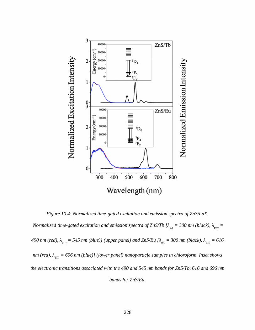
228
Figure 10.4: Normalized time-gated excitation and emission spectra of ZnS/LnX
Normalized time-gated excitation and emission spectra of ZnS/Tb [λex = 300 nm (black), λem =
490 nm (red), λem = 545 nm (blue)] (upper panel) and ZnS/Eu [λex = 300 nm (black), λem = 616
nm (red), λem = 696 nm (blue)] (lower panel) nanoparticle samples in chloroform. Inset shows
the electronic transitions associated with the 490 and 545 nm bands for ZnS/Tb, 616 and 696 nm
bands for ZnS/Eu.

10.3.8 ZnS Luminescence Lifetime Measurements
Luminescence lifetime parameters for the different systems studied are summarized in Table 1S
(see Supporting Information [51] ). Table 1S shows values for all parameters in a sum of three
exponentials varied in the fitting procedure. To see any obvious trend in the individual lifetime
components, the decay data were also fit to a sum of exponentials with lifetime components
fixed and varying only the amplitudes (Table 2S; see Supporting Information [51] ). This
procedure gives rise to somewhat lesser quality fits, as judged by the relative χ2 value being
higher; however, they are adequate and reveal a clear relationship between lifetime components
in the different systems. Note that the average lifetime remains relatively unchanged while
varying all parameters versus fixing the lifetime components in the fitting procedure. Some
representative luminescence decays for 1 min growth time samples are shown in Figure 10.5.
10.3.9 ZnS/Tb Samples
The samples obtained with 1 and 20 min growth time behave similarly in terms of the decay
kinetics. The experimental lifetime decays were typically fitted with the sum of three decaying
exponentials, with a subnanosecond component that comprises 60% of the emission; a 2−3 ns∼
component with 30% contribution; and the longest time component ( 10 ns), with an∼ ∼
amplitude of ≤ 10%. The average lifetime increases continuously with increasing λ∼ em, which
indicates that the emission band shifts with time. Attempts were made to monitor the Tb3+
emission by lowering the repetition rate to 100 kHz and increasing the full time window to 5∼
229
microseconds; in all cases, only the ZnS emission was significant, and no longer time
component, which might be related to the Tb3+ emission, was observed. At all wavelengths, only
the ZnS emission is important. Long-lived Tb3+ emission appears as a baseline, as shown in the
left panel in Figure 10.5 at 545 nm.
10.3.10 ZnS/Eu Samples
ZnS/Eu behaves differently compared with all other systems. Namely, the longer lifetimes are
more dominant in this sample, and the amplitude of the subnanosecond component is much
lower. This result suggests that a different energy transfer mechanism may take place. Balandin
and co-workers [20] used a theoretical investigation of ZnO quantum dots to predict an
increase in the radiative lifetime for a surface-bound ionized acceptor-exciton complex, as
compared with the lifetimes of confined excitons and surface-bound ionized donor-exciton
complexes. Such a type of complex would give rise to an increase in quantum yield. A
comparison of the overall quantum yield of ZnS/Eu3+ (0.27 ± 0.02) to that of ZnS/Tb3+ (0.12 ±
0.03) corroborates this conclusion. The lack of a long-lived baseline in the ZnS/Eu sample, as
compared with the ZnS/Tb sample, reflects the decreased luminescence of the Eu3+ bands in the
steady-state spectra (Figure 10.3D).
230
10.3.11 ZnS/Gd Samples
Because of an energy level mismatch between the donating energy levels of the nanoparticles
and the Gd3+ accepting levels, no Gd3+ luminescence is observed. The fact that the ZnS/Gd3+
sample’s nanoparticle emission is very similar to the ZnS emission of the ZnS/Tb3+ shows that
the ZnS properties are not sensitive to the presence and nature of the lanthanide cations.
10.3.12 ZnS Samples
The average lifetime of the ZnS sample is comparable to that of the corresponding value in the
presence of Tb3+ and Gd3+. The ZnS sample’s emission lifetime depends on λem in a fashion that
is similar to that found for the lanthanide-containing nanoparticles. Thus, the emission
wavelength dependence appears to be an intrinsic property of the nanoparticles and is not
associated with the presence of lanthanide ions (Tb3+, Eu3+, and Gd3+) in the system. The origin
of the shift might be caused by decays from different donor−acceptor pairs that vary in distance;
that is, close pairs emit with faster lifetime at higher energy, and the distant pairs emit at lower
energy.[20]
231
10.3.13 Lanthanide Ion Luminescence Lifetime Measurements
The luminescence lifetimes of the lanthanide cations were recorded using a low repetition rate
Nd:YAG laser-based setup. Experimental luminescence signals were fitted best by a
biexponential decay for Tb3+ and Eu3+. For ZnS/Tb3+, the luminescence lifetime values were
found to be 0.92 ± 0.01 and 2.50 ± 0.06 ms, whereas, for ZnS/Eu3+, the corresponding values
were 2.0 ± 0.01 and 3.6 ± 0.2 ms. The lifetimes for the Tb3+ emission band are similar to those
observed for CdSe/Tb3+ in a previous study.[19] Two components could arise from different
locations of the lanthanide ions in the nanoparticles; for example, Tb3+ in the core of the ZnS
nanoparticles may be better protected and have a longer luminescence lifetime, whereas the
shorter lifetime component may originate from the surface-located Tb3+, which experiences
more solvent quenching. Examples of lifetime values for molecular complexes with well-
protected Tb3+ and Eu3+ cation coordination sites are 1.3 and 0.78 ms, respectively.[56] The
longer lifetime values recorded in the nanoparticle samples suggest that the lanthanide ions are
better protected from quenching through vibrations located in solvent (and in the organic
sensitizer for molecular complexes) when in the nanoparticles, as was reported previously by
Chengelis et al. for CdSe/Tb3+.[19]
232
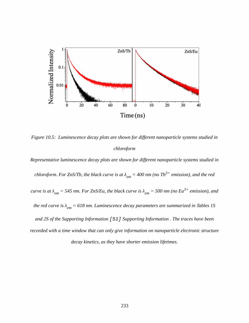
233
Figure 10.5: Luminescence decay plots are shown for different nanoparticle systems studied in
chloroform
Representative luminescence decay plots are shown for different nanoparticle systems studied in
chloroform. For ZnS/Tb, the black curve is at λem = 400 nm (no Tb3+ emission), and the red
curve is at λem = 545 nm. For ZnS/Eu, the black curve is λem = 500 nm (no Eu3+ emission), and
the red curve is λem = 618 nm. Luminescence decay parameters are summarized in Tables 1S
and 2S of the Supporting Information [51] Supporting Information . The traces have been
recorded with a time window that can only give information on nanoparticle electronic structure
decay kinetics, as they have shorter emission lifetimes.
10.3.14 A Mechanism for Sensitization of Lanthanide Luminescence
This section considers the possibility of Förster (dipole−dipole interaction) and Dexter (exchange
interaction) electronic energy transfer mechanisms in the studied systems, but argues that a
different mechanism operates.
The rate of energy transfer under the Förster formulation depends on (a) the spectral
overlap of donor and acceptor (JF), (b) the donor luminescence quantum yield, (c) the donor
luminescence lifetime, (d) the relative orientation of donor and acceptor transition dipoles, and
(e) the distance between donor and acceptor. Most of the lanthanide transitions (dipolar electric)
are formally forbidden and, thus, have a low oscillator strength and a low energy transfer rate by
the Förster mechanism. The Förster overlap integral is JF 10∼ −19−10−20 M−1 cm3 for the
systems studied here, whereas the typical value of JF for organic fluorophores is on the order of
10−13−10−15 M−1 cm3.[82] Assuming a ΦD = 0.2, one calculates an R0 of 2.5 Å for a∼
lanthanide, which should be compared with a value of R0 = 25 Å for a typical organic
fluorophore. The ratio of the rate of energy transfer for organic fluoropohores in comparison with
the ZnS/Tb3+ nanoparticle samples is 10∼ 6. On the basis of this estimate, we conclude that the
Förster mechanism is less likely to play a significant role in the energy transfer process for the
systems investigated in the present study. More straightforward evidence against the operation of
the Förster energy transfer mechanism can be established from a comparison of JF and R0 values
in the different systems studied (see Table 3S in the Supporting Information [51] ). The Förster
234
model predicts that the Eu3+ sensitization should be larger than Tb3+ in ZnS nanoparticles for a
given distance, by 3 times; in contrast, the experiments show that Tb∼ 3+ is at least 2-fold more
luminescent than Eu3+ (vide infra). In addition, a comparison of the host nanoparticles (ZnS,
ZnSe, CdS, CdSe) indicates that the rate of energy transfer to Tb3+ should be very similar in ZnS
and CdS; however, experiments demonstrate that ZnS is more efficient than CdS in sensitizing
Tb3+ luminescence (Figure 10.6). It has been assumed that both the nanoparticles have similar
luminescence lifetime in absence of acceptors and Tb3+ resides at almost equal distance from the
nanoparticle sensitizing center.
The rate of energy transfer for the Dexter formulation depends on (a) the spectral overlap
of donor emission and acceptor absorption (JD) and (b) the electronic coupling factor. The
Dexter mechanism can account for energy transfer involving forbidden transitions. The fact that
the calculated JD values are very similar in the different systems indicates that the experimental
trend in energy transfer rates among the different nanoparticles can only be explained by a
concomitant change in the electronic coupling parameter. Although this possibility cannot be
excluded, it seems unlikely. Thus, it seems that both the Förster and Dexter energy transfer
mechanisms play a negligible role in the energy transfer mechanism of the studied systems.
A number of other plausible mechanisms for luminescence sensitization in rare earth ions
in semiconductors have been proposed. For example, Klik et al., in the context of InP/Yb3+,
[42] rationalized Yb3+ sensitization in InP by this mechanism: (a) excitation of the
semiconductor from the valence band to conduction band; (b) capturing of a free electron at a
Yb3+ related trap; (c) generation of an electron−hole pair on the trap; and (d) nonradiative
235
recombination of electron−hole pair to excite the Yb3+, thus generating the Yb3+ emission. This
model was based on earlier studies by Palm et al.,[53] Takahei and co-workers,[73; 82]
Thonke et al.,[78] and Needels et al.[52] In molecular systems, Lazarides et al. has
discussed a redox-based energy transfer mechanism in the context of molecular d−f complexes.
[45] Mechanisms of this type require a detailed knowledge of the dopant energy levels in the
host semiconductor.
Although much has been discussed about the lanthanide sensitization in semiconductor
materials, considerably less is known about the energy level positions of lanthanide ions in the
host material.[54; 62; 75-77] The location of dopant ion energy levels with respect to
the valence and conduction bands of the host lattice is of extreme importance because it is useful
for predicting the luminescence properties and the charge trapping and detrapping kinetics.
Recently, Dorenbos [22-27] addressed the problem of locating lanthanide impurity levels in a
host crystal semiempirically and developed a model that relies on three host dependent
parameters: (a) the charge transfer energy from the anion valence band to Eu3+, (b) the redshift
of the first 4f to 5d transition in appropriate lanthanide ions, and (c) the band gap of the
semiconductor material. The fundamental assumptions in this method are that the binding
energies of the 4f electrons follow a universal trend and that the charge transfer energy between
the anion valence band and Eu3+ is equal to the energy gap between the valence band of the host
material and the ground state of Eu2+. Once the Eu2+ ground state energy level is assigned, all
other energy levels can be predicted according to the trend in binding energies.
236
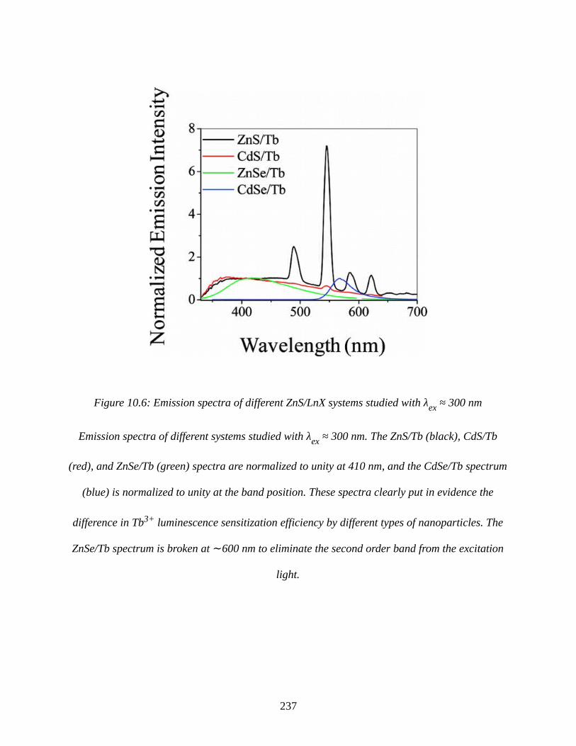
237
Figure 10.6: Emission spectra of different ZnS/LnX systems studied with λex ≈ 300 nm
Emission spectra of different systems studied with λex ≈ 300 nm. The ZnS/Tb (black), CdS/Tb
(red), and ZnSe/Tb (green) spectra are normalized to unity at 410 nm, and the CdSe/Tb spectrum
(blue) is normalized to unity at the band position. These spectra clearly put in evidence the
difference in Tb3+ luminescence sensitization efficiency by different types of nanoparticles. The
ZnSe/Tb spectrum is broken at 600 nm to eliminate the second order band from the excitation∼
light.
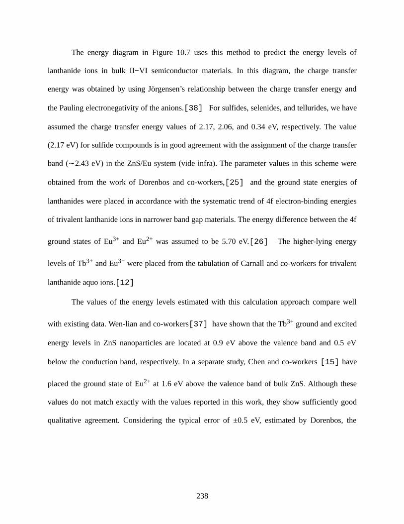
The energy diagram in Figure 10.7 uses this method to predict the energy levels of
lanthanide ions in bulk II−VI semiconductor materials. In this diagram, the charge transfer
energy was obtained by using Jörgensen’s relationship between the charge transfer energy and
the Pauling electronegativity of the anions.[38] For sulfides, selenides, and tellurides, we have
assumed the charge transfer energy values of 2.17, 2.06, and 0.34 eV, respectively. The value
(2.17 eV) for sulfide compounds is in good agreement with the assignment of the charge transfer
band ( 2.43 eV) in the ZnS/Eu system (vide infra). The parameter values in this scheme were∼
obtained from the work of Dorenbos and co-workers,[25] and the ground state energies of
lanthanides were placed in accordance with the systematic trend of 4f electron-binding energies
of trivalent lanthanide ions in narrower band gap materials. The energy difference between the 4f
ground states of Eu3+ and Eu2+ was assumed to be 5.70 eV.[26] The higher-lying energy
levels of Tb3+ and Eu3+ were placed from the tabulation of Carnall and co-workers for trivalent
lanthanide aquo ions.[12]
The values of the energy levels estimated with this calculation approach compare well
with existing data. Wen-lian and co-workers[37] have shown that the Tb3+ ground and excited
energy levels in ZnS nanoparticles are located at 0.9 eV above the valence band and 0.5 eV
below the conduction band, respectively. In a separate study, Chen and co-workers [15] have
placed the ground state of Eu2+ at 1.6 eV above the valence band of bulk ZnS. Although these
values do not match exactly with the values reported in this work, they show sufficiently good
qualitative agreement. Considering the typical error of ±0.5 eV, estimated by Dorenbos, the
238

agreement with the available literature is reasonable. It has to be noted that as long as any
systematic error in assigning these energy level values is relatively constant, it should not change
the conclusions discussed here.
239
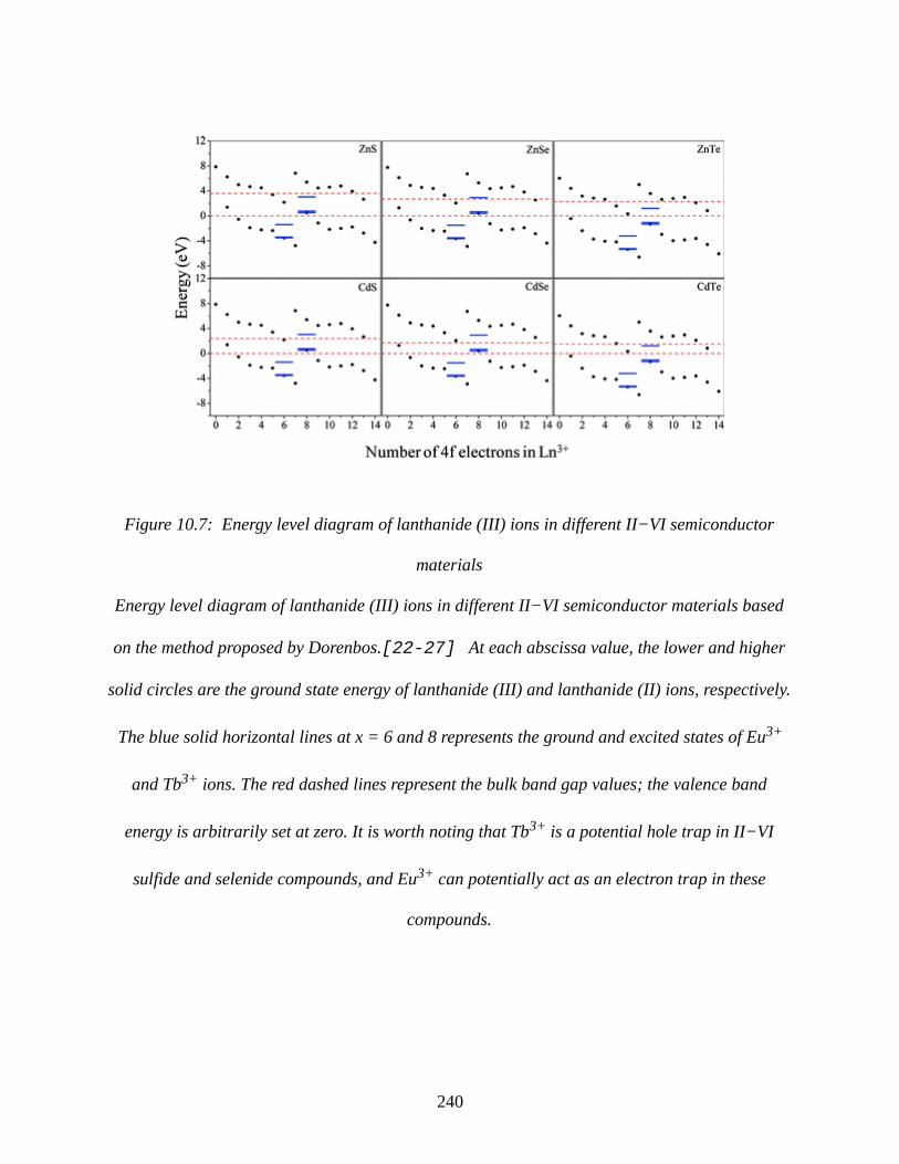
240
Figure 10.7: Energy level diagram of lanthanide (III) ions in different II−VI semiconductor
materials
Energy level diagram of lanthanide (III) ions in different II−VI semiconductor materials based
on the method proposed by Dorenbos.[22-27] At each abscissa value, the lower and higher
solid circles are the ground state energy of lanthanide (III) and lanthanide (II) ions, respectively.
The blue solid horizontal lines at x = 6 and 8 represents the ground and excited states of Eu3+
and Tb3+ ions. The red dashed lines represent the bulk band gap values; the valence band
energy is arbitrarily set at zero. It is worth noting that Tb3+ is a potential hole trap in II−VI
sulfide and selenide compounds, and Eu3+ can potentially act as an electron trap in these
compounds.

To determine the charge transfer energy from the anion valence band to Eu3+, the
excitation spectra of ZnS/Tb and ZnS/Eu were compared (see Figure 10.8). The band at 510∼
nm is assigned to a charge transfer band of Eu3+ in the ZnS/Eu system. Note that the red-shifted
emission spectrum for ZnS/Eu systems with λex = 300 nm could arise from its charge transfer
nature. Circumstantial evidence for this assignment in the ZnS/Eu system comes from a
comparison of Tb3+ and Eu3+ emission intensities with different excitation wavelengths (see
Table 4S in the Supporting Information [51] ). While the intensity of the Tb3+ luminescence
decreases sharply when exciting the sample with lower energy than the bandgap of the ZnS
nanoparticles, the situation is different for the ZnS/Eu system. Considerable luminescence
intensity was observed from Eu3+ in ZnS nanoparticles, even while exciting the sample at longer
wavelength values. Although this observation does not directly prove the existence of a charge
transfer band in the ZnS/Eu system, it strongly suggests that some energy level located lower
than the bandgap of ZnS nanoparticles exists, and it is involved in the sensitization of Eu3+ in the
ZnS doped nanoaparticles.
241
242
Figure 10.8: Normalized steady-state excitation spectra of ZnS/Tb nanoparticles
Normalized steady-state excitation spectra of ZnS/Tb nanoparticles with λem = 545 (black) and
620 nm (red). The green and blue curves are the corresponding spectra for ZnS/Eu
nanoparticles. Spectra are normalized arbitrarily to the maximum intensity
Several features of the energy level diagram in Figure 10.7 are noteworthy:
1. Both the ground and excited states of Tb3+ lie within the band gap of bulk ZnS, an effect
that should be more pronounced in nanoparticles because of the quantum confinement
and, hence, a higher band gap ( 4.2 eV as opposed to 3.6 eV for bulk material). This∼
indicates that the Tb3+ can potentially act as a hole trap in ZnS. Moreover, it suggests that
the excited electron in the 5D4 level of Tb3+ does not undergo ready autoionization. These
two conditions result in the enhancement of the Tb3+ luminescence in ZnS. It is generally
believed that the luminescence efficiency of lanthanide ions is increased when their 3+
levels act as trap states.[73]
2. The 5D4 level of Tb3+ lies above the conduction band of CdSe so that autoionization of
the Tb3+* should be efficient, thereby decreasing its luminescence efficiency.
Experimentally, the ZnS/Tb3+ emission is much stronger than the CdSe/Tb3+ emission,
for which the overall quantum yields of ZnS/Tb3+ and CdSe/Tb3+ are 0.12 ± 0.03 and
0.025 ± 0.001, respectively, whereas the Tb3+ contribution to the overall quantum yield
were found to be 0.05 ± 0.01 and 0.000 015 ± 0.000 003. It should also be noted that the
time-gated mode is required to observe the Tb3+ emission in CdSe/Tb3+,[19] whereas
they were readily observable in steady-state mode for ZnS/Tb3+ luminescence.
3. The energy level locations of Eu3+ are qualitatively different from Tb3+ in ZnS, because
both the ground and excited states of Eu3+ lie below the valence band of ZnS. It is
important to note that the ground state of Eu2+ lies within the band gap of ZnS, which
243

makes the system a potential electron trap. On the basis of these considerations, Eu3+ can
be brought to the excited state by two possible pathways: (1) a bandgap transition of the
ZnS host and (2) a ZnS valence band to Eu2+ ground state transition. Our observations
are consistent with either of these mechanisms.
4. ZnS should be more efficient than ZnSe in sensitizing Tb3+ luminescence because as the
excited energy level of Tb3+ lies close to the conduction band of ZnSe, the excited
electrons face a competitive nonradiative path of autoionization. To test this hypothesis,
ZnSe/Tb nanoparticles were prepared. The measured Tb3+ lanthanide-centered quantum
yield value for ZnSe/Tb is 0.000 18 ± 0.000 07 as compared with 0.05 ± 0.01 for ZnS/Tb
system, validating this prediction.
5. On the basis of the energy level diagrams, CdS should be more efficient in sensitizing
Tb3+ luminescence than is CdSe, but similar or less efficient than ZnS. To check this
prediction, experiments with the CdS/Tb system were undertaken. Results from these
experiments are shown in Figure 10.9. Sharp Tb3+ bands are clearly visible at 490 and
545 nm. Interestingly, a band shift in the time-gated excitation spectra with the growth
time of nanoparticles is evident and attributed to the effect of quantum confinement. This
shift unequivocally points toward the presence of an antenna effect for the Tb3+
sensitization. Moreover, on the basis of the ratio of bandgaps and Tb3+ emission
intensities, it is apparent that the ZnS is more efficient than CdS in sensitizing Tb3+
luminescence, which is consistent with the prediction based on the energy level diagrams.
The ratio of ZnS bandgap emission to the Tb3+ luminescence at 545 nm in ZnS and∼
CdS was found to be 1:10:1.4.
244
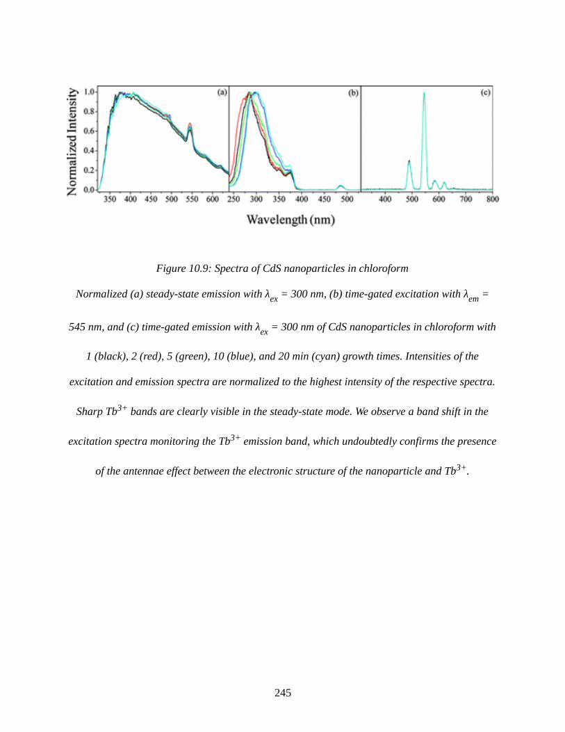
245
Figure 10.9: Spectra of CdS nanoparticles in chloroform
Normalized (a) steady-state emission with λex = 300 nm, (b) time-gated excitation with λem =
545 nm, and (c) time-gated emission with λex = 300 nm of CdS nanoparticles in chloroform with
1 (black), 2 (red), 5 (green), 10 (blue), and 20 min (cyan) growth times. Intensities of the
excitation and emission spectra are normalized to the highest intensity of the respective spectra.
Sharp Tb3+ bands are clearly visible in the steady-state mode. We observe a band shift in the
excitation spectra monitoring the Tb3+ emission band, which undoubtedly confirms the presence
of the antennae effect between the electronic structure of the nanoparticle and Tb3+.
10.4 CONCLUSION
An efficient and less toxic luminescent lanthanide system, consisting of ZnS nanoparticles with
incorporated lanthanide ions, has been established. Efficient sensitization was observed for both
the ZnS/Tb3+ and the ZnS/Eu3+ systems. The ZnS/Tb3+ nanoparticles appear to be more efficient
lanthanide-based emitters, with lanthanide-centered quantum yield values for ZnS/Tb3+ and
ZnS/Eu3+ being 0.05 ± 0.01 and 0.000 13 ± 0.000 04, respectively. Excitation spectra, while
monitoring the lanthanide emission, clearly reveal that ZnS nanoparticles act as an antenna to
sensitize the lanthanide luminescence in these systems. Moreover, the absence of observable
sharp bands in the excitation spectra indicate that direct excitation of lanthanides has a negligible
contribution to the overall sensitization mechanism. These systems represent a significant
improvement over the originally proposed system CdSe/Tb3+ in their efficiency for lanthanide
luminescence sensitization.
The mechanism of lanthanide luminescence sensitization in II−VI semiconductor
materials can be rationalized by a semiempirical method proposed by Dorenbos and co-workers.
Energy level diagrams indicate that in ZnS, Tb3+ can act as a potential hole trap and provide a
dramatic increase in sensitization efficiency because its energy levels lie between the
nanoparticle band edges. The mechanism of Eu3+ luminescence sensitization, on the other hand,
follows a different type of mechanism. In ZnS, Eu3+ can act as a potential electron trap; hence,
the sensitization can be achieved either by direct bandgap excitation or by a valence band to
246

Eu2+ transition. Either mechanism can explain the experimental observations in the ZnS/Eu
system. A comparison of lanthanide efficiency in ZnS nanoparticles is made with respect to other
II−VI materials. Emphasis is given to Tb3+-doped ZnSe and CdS nanoparticles, both being less
efficient than the ZnS nanoparticles in sensitizing the Tb3+ luminescence, which is consistent
with the predictions based on the energy level positions.
247

10.5 BIBLIOGRAPHY
[1] Abiko, Y.; Nakayama, N.; Akimoto, K. and Yao, T. (2002). , Phys. Status Solidi, B 229 : 339.
[2] Anderson, W. W. (1964). , Phys. Rev. 136 : A556.
[3] Beeby, A.; Clarkson, I. M.; Dickins, R. S.; Faulkner, S.; Parker, D.; Royle, L.; de Sousa, A. S.; Williams, J. A. G. and Woods, M. (1999). , J. Chem. Soc., Perkin Trans. 2 : 493.
[4] Bhargava, R. N. (1996). , J. Lumin. 70 : 85.
[5] Binnemans, K. (2009). , Chem. Rev. 109 : 4283.
[6] Bol, A. A.; van Beek, R. and Meijerink, A. (2002). , Chem. Mater. 14 : 1121.
[7] Brennan, J. D.; Capretta, A.; Yong, K.; Gerritsma, D.; Flora, K. K. and Jones, A. (2002). , Photochem. Photobiol. 75 : 117.
[8] Brus, L. E. (1984). , J. Chem. Phys. 80 : 4403.
[9] Bünzli, J.-C. G. (2010). , Chem. Rev. 110 : 2729.
[10] Bünzli, J.-C. G. and Piguet, C. (2005). , Chem. Soc. Rev. 34 : 1048.
[11] Carnall, W. T. and Fields, P. R., 1967. Lanthanide/Actinide Chemistry. American Chemical Society, .
[12] Carnall, W. T.; Fields, P. R. and Rajnak, K. (1968). , J. Chem. Phys. 49 : 4450.
[13] Chen, L.; Zhang, J.; Lu, S.; Ren, X. and Wang, X. (2005). , Chem. Phys. Lett. 409 : 144.
[14] Chen, W.; Joly, A. G.; Malm, J.-O. and Bovin, J.-O. (2004). , J. Appl. Phys. 95 : 667.
[15] Chen, W.; Malm, J.-O.; Zwiller, V.; Huang, Y.; Liu, S.; Wallenberg, R.; Bovin, J.-O. and Samuelson, L. (2000). , Phys. Rev. B 61 : 11021.
[16] Chen, W.; Wang, Z.; Lin, Z. and Lin, L. (1997). , J. Appl. Phys. 82 : 3111.
[17] Chen, Y. and Lu, Z. (2007). , Anal. Chim. Acta 587 : 180.
[18] Chen, Y. S.; Burgiel, J. C. and Kahng, D. (1970). , J. Electrochem. Soc.: Solid State Science 117 : 794.
248

[19] Chengelis, D. A.; Yingling, A. M.; Badger, P. D.; Shade, C. M. and Petoud, S. (2005). , J. Am. Chem. Soc. 127 : 16752.
[20] Chestnoy, N.; Harris, T. D.; Hull, R. and Brus, L. E. (1986). , J. Phys. Chem. 90 : 3393.
[21] Dong, L.; Liu, Y.; Zhuo, Y. and Chu, Y. (2010). , Eur. J. Inorg. Chem. : 2504.
[22] Dorenbos, P. (2003). , J. Phys.: Condens. Matter 15 : 8417.
[23] Dorenbos, P. (2004). , J. Lumin. 108 : 301.
[24] Dorenbos, P. (2005). , J. Lumin. 111 : 89.
[25] Dorenbos, P. (2009). , J. Alloys Compd. 488 : 568.
[26] Dorenbos, P. and van der Kolk, E. (2006). , Appl. Phys. Lett. 89 : 061122-1−061122-3.
[27] Dorenbos, P. and van der Kolk, E. (2008). , Opt. Mater. 30 : 1052.
[28] Ehrhart, G.; Capoen, B.; Robbe, O.; Beclin, F.; Boy, P.; Turrell, S. and Bouazaoui, M. (2008). , Opt. Mater. 30 : 1595.
[29] Eliseeva, S. V. and Bünzli, J.-C. G. (2010). , Chem. Soc. Rev. 39 : 189.
[30] Fonoberov, V. A. and Balandin, A. A. (2004). , Appl. Phys. Lett. 85 : 5971.
[31] Fuhs, W.; Ulber, I.; Weiser, G.; Bresler, M. S.; Gusev, O. B.; Kuznetsov, A. N.; Kudoyarova, V. K.; Terukov, E. I. and Yassievich, I. N. (1997). , Phys. Rev. B 56 : 9545.
[32] Godlewski, M.; Światek, K. and Monemar, B. (1994). , J. Lumin. 58 : 303.
[33] Godlewski, M.; Zakrzewski, A. J. and Ivanov, V. Y. (2000). , J. Alloys Compd. 300−301 : 23.
[34] Gregorkiewicz, T.; Thao, D. T. X.; Langer, J. M.; Bekman, H. H. P. T.; Bresler, M. S.; Michel, J. and Kimerling, L. C. (2000). , Phys. Rev. B 61 : 5369.
[35] Hildebrandt, N. and Löhmannsröben, H.-G. (2007). , Curr. Chem. Biol. 1 : 167.
[36] Hou, S.; Yuen, Y.; Mao, H.; Wang, J. and Zhu, Z. (2009). , J. Phys. D: Appl. Phys. 42 : 215105.
[37] Jing-hua, N.; Rui-nian, H.; Wen-lian, L.; Ming-tao, L. and Tian-zhi, Y. (2006). , J. Phys. D: Appl. Phys. 39 : 2357.
[38] Jörgensen, C. K., 1971. Modern Aspects of Ligand Field Theory. , .
[39] Kahng, D. (1968). , Appl. Phys. Lett. 13 : 210.
[40] Kallmann, H. and Luchner, K. (1961). , Phys. Rev. 123 : 2013.
249

[41] Kim, Y. H.; Baek, N. S. and Kim, H. K. (2006). , Chem. Phys. Chem. 7 : 213.
[42] Klik, M. A. J.; Gregorkiewicz, T.; Bradley, I. V. and Wells, J.-P. R. (2002). , Phys. Rev. Lett. 89 : 227401-1−227401-4.
[43] Krupka, D. C. (1972). , J. Appl. Phys. 43 : 476.
[44] Kühne, H.; Weiser, G.; Terukov, E. I.; Kusnetsov, A. N. and Kudoyarova, V. K. (1999). , J. Appl. Phys. 86 : 896.
[45] Lazarides, T.; Tart, N. M.; Sykes, D.; Faulkner, S.; Barbieri, A. and Ward, M. D. (2009). , Dalton Trans. : 3971.
[46] Li, L. S.; Pradhan, N.; Wang, Y. and Peng, X. (2004). , Nano Lett. 4 : 2261.
[47] Luchner, K. M.; Kallmann, H. P.; Kramer, B. and Wachter, P. (1963). , Phys. Rev. 129 : 593.
[48] Meech, S. R. and Phillips, D. C. (1983). , J. Photochem. 23 : 229.
[49] Montgomery, C. P.; Murray, B. S.; New, E. J.; Pal, R. and Parker, D. (2009). , Acc. Chem. Res. 42 : 925.
[50] Moore, E. G.; Samuel, A. P. S. and Raymond, K. N. (2009). , Acc. Chem. Res. 42 : 542.
[51] Mukherjee, P.; Shade, C. M.; Yingling, A. M.; Lamont, D. N.; Waldeck, D. H. and Petoud, S. (2011). Lanthanide sensitization in II−VI semiconductor materials: A case study with Terbium(III) and Europium(III) in zinc sulfide nanoparticles, The Journal of Physical Chemistry A 115 : 4031-4041.
[52] Needels, M.; Schlüter, M. and Lannoo, M. (1993). , Phys. Rev. B 47 : 15533.
[53] Palm, J.; Gan, F.; Zheng, B.; Michel, J. and Kimerling, L. C. (1996). , Phys. Rev. B 54 : 17603.
[54] Pedrini, C.; Bouttet, D.; Dujardin, C.; Belsky, A.; Vasil’ev, A.; Dorenbos, P. and van Eijk, C. W. E., 1996. Proc. Int. Conf. Inorg. Scintillators,.
[55] Petoud, S.; Cohen, S. M.; Bünzli, J.-C. G. and Raymond, K. N. (2003). , J. Am. Chem. Soc. 125 : 13324.
[56] Petoud, S.; Muller, G.; Moore, E. G.; Xu, J.; Sokolnicki, J.; Riehl, J. P.; Le, U. N.; Cohen, S. M. and Raymond, K. N. (2007). , J. Am. Chem. Soc. 129 : 77.
[57] Planelles-Aragó, J.; Julián-López, B.; Cordoncillo, E.; Escribano, P.; Pellé, F.; Viana, B. and Sanchez, C. (2008). , J. Mater. Chem. 18 : 5193.
[58] Przybylinska, H. and Godlewski, M. (1987). , Phys. Rev. B 36 : 1677.
250

[59] Przybylińska, H.; Świ tek, K.; St por, A.; Suchocki, A. and Godlewski, M.aa aa (1989). , Phys. Rev. B 40 : 1748.
[60] Qu, S. C.; Zhou, W. H.; Liu, F. Q.; Chen, N. F.; Wang, Z. G.; Pan, H. Y. and Yu, D. P. (2002). , Appl. Phys. Lett. 80 : 3605.
[61] Richardson, F. S. (1982). , Chem. Rev. 82 : 541.
[62] Sato, S. (1976). , J. Phys. Soc. Jpn. 41 : 913.
[63] Sato, S. and Wada, M. (1970). , Bull. Chem. Soc. Jpn. 43 : 1955.
[64] Sivakumar, S.; van Veggel, F. C. J. M. and Raudsepp, M. (2007). , Chem. Phys. Chem. 8 : 1677.
[65] Sooklal, K.; Cullum, B. S.; Angel, S. M. and Murphy, C. J. (1996). , J. Phys. Chem. 100 : 4551.
[66] Streetman, B. G. and Banerjee, S., 2000. Solid State Electronic Devices. , .
[67] Sun, L.; Yan, C.; Liu, C.; Liao, C.; Li, D. and Yu, J. (1998). , J. Alloys Compd. 275−277 : 234.
[68] Sun, X. L.; Zhang, G. L.; Tang, G. Q. and Chen, W. J. (1999). , Chin. Chem. Lett. 10 : 807.
[69] Światek, K. and Godlewski, M. (1990). , Appl. Phys. Lett. 56 : 2192.
[70] Świ tek, K.; Godlewski, M. and Hommel, D.aa (1990). , Phys. Rev. B 42 : 3628.
[71] Światek, K.; Suchocki, A. and Godlewski, M. (1990). , Appl. Phys. Lett. 56 : 195.
[72] Światek, K.; Suchocki, A.; Przybylinska, H. and Godlewski, M. (1990). , J. Cryst. Growth 101 : 435.
[73] Takahei, K.; Taguchi, A.; Nakagome, H.; Uwai, K. and Whitney, P. S. (1989). , J. Appl. Phys. 66 : 4941.
[74] Thibon, A. and Pierre, V. C. (2009). , Anal. Bioanal. Chem. 394 : 107.
[75] Thiel, C. W.; Cruguel, H.; Sun, Y.; Lapeyre, G. J.; Macfarlane, R. M.; Equall, R. W. and Cone, R. L. (2001). , J. Lumin. 94/95 : 1.
[76] Thiel, C. W.; Cruguel, H.; Wu, H.; Sun, Y.; Lapeyre, G. J.; Cone, R. L.; Equall, R. W. and Macfarlane, R. M. (2001). , Phys. Rev. B 64 : 085107-1−085107-13.
[77] Thiel, C. W.; Sun, Y. and Cone, R. L. (2002). , J. Mod. Opt. 49 : 2399.
[78] Thonke, K.; Pressel, K.; Bohnert, G.; Stapor, A.; Weber, J.; Moser, M.; Molassioti, A.; Hangleiter, A. and Scholz, F. (1990). , Sernicond. Sci. Technol. 5 : 1124.
251

[79] Tsimperidis, I.; Gregorkiewicz, T.; Bekman, H. H. P. T. and Langerak, C. J. G. M. (1998). , Phys. Rev. Lett. 81 : 4748.
[80] Wang, L.; Xu, X. and Yuan, X. (2010). , J. Lumin. 130 : 137.
[81] White, K. A.; Chengelis, D. A.; Gogick, K. A.; Stehman, J.; Rosi, N. L. and Petoud, S. (2009). , J. Am. Chem. Soc. 131 : 18069.
[82] Whitney, P. S.; Uwai, K.; Nakagome, H. and Takahei, K. (1988). , Appl. Phys. Lett. 53 : 2074.
[83] Xueyuan, C.; Wenqin, L.; Yongsheng, L. and Guokui, L. (2007). , J. Rare Earths 25 : 515.
[84] Yang, C.; Fu, L.-M.; Wang, Y.; Zhang, J.-P.; Wong, W.-T.; Ai, X.-C.; Qiao, Y.-F.; Zou, B.-S. and Gui, L.-L. (2004). , Angew. Chem., Int. Ed. 43 : 5010.
[85] Yang, H.; Yu, L.; Shen, L. and Wang, L. (2004). , Mater. Lett. 58 : 1172.
[86] Yassievich, I.; Bresler, M. and Gusev, O. (1998). , J. Non-Cryst. Solids 226 : 192.
252
11.0 THROUGH SOLVENT TUNNELING IN DONOR-
BRIDGE-ACCEPTOR MOLECULES CONTAINING A
MOLECULAR CLEFT
Author list: Brittney M Graff, Daniel N. Lamont, Matthew F. L. Parker, Brian P. Bloom,
Christian E. Schafmeister, and David H. Waldeck
Author contribution: The author of this dissertation contributed to the photophysical
characterization of the molecules, interpretation of the results and the preparation of the
manuscript. The author was responsible for the quantum chemistry simulations. This work has
been published at J. Phys. Chem. A 2016, 120, 6004
11.1 INTRODUCTION
Electron-transfer (ET) reactions are essential to many chemical and biological transformations. A
nonzero electronic coupling |V| between an electron donor (D) and acceptor (A) unit is a
prerequisite for electron-transfer reactions. As detailed by Marcus and others, [18] the
strength of the electronic coupling is generally used to categorize ET reactions into a strong
coupling or adiabatic charge-transfer regime for which |V| > > kT, an intermediate regime for
253
which |V| is comparable to kT, and a weak coupling/ nonadiabatic regime for which |V| < kT; the
latter is relevant to the systems discussed herein. In the nonadiabatic limit the ET rate constant
may be written as
where FCWDS is the Franck-Condon factor, which contains parameters related to molecular
structure and environmental variables. The electronic coupling magnitude may be mediated by
covalent and/or noncovalent interactions and depends on the electronic features of the medium
through which the electron tunnels. Although often weaker than bond-mediated coupling
pathways, electron-transfer involving solvent molecules in the electron tunneling pathway is
likely to play an important role for intermolecular electron transfer reactions; consequently, the
solvent’s electronic structure can play an important role in the ET kinetics.
Over the past three decades the study of well-defined synthetic donor-bridge-acceptor
(DBA) systems has led to a better understanding of ET mechanisms and kinetics in nonpolar
solvents. Investigations of conformationally restricted linear DBA molecules [12; 16; 32;
34; 43] have demonstrated the distance dependence of bond-mediated coupling. Analogous
studies with cleft containing molecules have demonstrated electron tunneling through non-
bonded contacts. For C-shaped DBA molecules, in which the D and A units are separated by a
solvent-accessible cleft;[8; 30; 35; 45] such coupling appears to be strongest when a
single solvent molecule occupies the cleft. The dependence of |V| on the molecular orbital
254
k ET=2 πℏ
∙|V|2∙ FCWDS
Equation 11.1
energetics of the solvent molecule involved in the electron tunneling event has been studied
using both C-shaped DBA molecules [30] and U-shaped DBA systems, for which a pendant
group is fixed inside the cleft.[6; 31] The U-shaped systems have been used to tune the
electronic coupling from the weak (nonadiabatic) limit to the strong (adiabatic) limit and to
examine the important role played by solvent dynamics. [7; 25] DBA systems, which
demonstrate the influence of macromolecular structural fluctuations on ET rates, have been
studied as well.[2; 3; 37] The studies reported here are distinguished from these earlier
studies by examining solvent mediated coupling in water and polar solvents.
While early studies examined through solvent coupling in frozen media,
conformationally restricted DBA systems provide a way to examine solvent mediated ET in fluid
media. The use of rigid C-shaped molecules facilitates the study of solvent-mediated electron
transfer by limiting the conformational freedom of the D and A moieties. In many rigid DBA
systems, the rate of the DBA systems’ structural fluctuations that might affect |V| is fast
compared to ket; so that an average value for |V|2 can be used to describe the electronic coupling.
In a previous study,[8] the shape of a DBA bis-amino acid oligomer was tailored to produce a
well-defined cleft with a line-of-site donor-acceptor distance that was just large enough to
accommodate a single water molecule. The observed electron-transfer rate constant in water was
significantly higher than in DMSO and was attributed to water molecule(s) in the cleft between
the donor and acceptor to mediate the electronic coupling.
This study explores how the photoinduced ET rates of two rigid C-shaped DBA bis-
amino acid oligomers are affected by polar solvents. The two compounds have similar donor
and acceptor groups but different topologies caused by chiral inversions of two bridge
stereocenters. The DBA system D-SSS-A, 1, forms a molecular cleft with a distance of about 6
255
Å between the donor and acceptor; whereas the D-RSS-A, 2, molecule has a more open and
flexible cleft (see Figure 11.1 for a molecular structure). These two molecules are similar to the
DBA systems reported in a previous study [8], but they display different cleft properties and
redox energetics by variation of the acceptor unit. The bis-amino acid bridge units and electron
donor moiety, dimethylaniline (DMA), are unchanged from the earlier study. The acceptor unit
is attached to the bridge, via a carboxamide moiety, however a methylacetamide substitution is
made at the C-6 of the pyrene in an attempt to shift the reaction energetics and modulate the
properties of the cleft. This feature allows the reaction Gibbs energy to be extracted from the
kinetic data directly and to examine how cleft site polarity affects the solvent mediated electron
transfer.
256

257
Figure 11.1: PL spectra and molecular structures of compound 1, 2, and 3
The figure shows photoluminescence (PL) spectra for aqueous solutions of 1 (A), 2 (B), and 3 (C) at
excitation wavelengths of 330 nm (dotted), 375 nm (solid), and 400 nm (dashed). Molecular structures for
1, 2, and 3 are shown in the upper portion of each panel. The spectra have been OD corrected and the
emission intensity has been scaled for convenience; note that the relative magnitudes of the emission
intensity between the panels are accurately reflected by the intensity scale.
11.2 EXPERIMENTAL
11.2.1 Synthesis
Compounds 1, 2, and 3 were prepared using a solid phase peptide chemistry utilizing a 2-
chlorotrityl chloride resin similar to that which is described in Chakrabarti et. al.[8] Due to
the hydrophilic nature of the compounds, they were liberated from the resin with all protecting
groups intact and purified using HPLC, followed by deprotection and subsequent HPLC
purification. The final compounds were assessed for identity and purity using NMR and LCMS
techniques. The functional pyrene carboxylic acid used to make compounds 1-4 was synthesized
in 5 synthetic steps and isolated from a mixture of regioisomers. The regiochemistry of the
isomer was confirmed using 2D-NMR (See section S3 of the Supplemental Information). All
other components used to assemble compounds 1-4 were obtained from commercial sources or
have been previously described.6 Compound 4 was prepared using standard solution phase
acylation conditions from the same pyrene precursor. See section S1 of the Supplemental
Information for more detail on the synthesis and molecule characterization.
Fmoc-Lys(Boc)-OH and Fmoc-Gly-OH were purchased from Novabiochem. O-(7-
azabenzo-triazole-1-yl)-N, N,N’N’-tetramethyluronium hexafluorophosphate (HATU) and 2-
Chlorotrityl chloride resin were purchased from Genscript. Hexafluoro-2-propanol was
purchased from Oakwood. All other reagents were purchased from Sigma Aldrich.
258

An ISCO CombiFlash Companion was utilized to perform flash chromatography. The
cartridges were filled with Bodman 32-63 D grade silica gel. A Waters Xterra MS C18 column
(3.5 um packing, 4.6 mm x 100 mm) was utilized with a Hewlett-Packard Series 1200 for HPLC-
MS analysis. The solvent system of acetonitrile/water (0.1% formic acid) had a flow rate of 0.8
mL/min. A Waters Xterra column (5um packing, 19 mm X 100 mm) was utilized with the Varian
Prostar Prep HPLC system to carry out preparatory scale HPLC purification. The solvent system
of acetonitrile/water (0.1% formic acid) had a flow rate of 12 mL/min. A Bruker 500 MHz NMR
was utilized to perform NMR experiments. The chemical shifts (δ) reported are relative to the
residual solvent peak of the solvent utilized; either DMSO-d6 or CDCl3. HRESIQTOFMS (high
resolution quadrupole time of flight mass spectrometry) analysis was performed at Ohio State
University.
11.2.2 Photophysics
Water used in all experiments was purified by a Barnstead Nanopure system, and its resistance
was 18.2 MΩ-cm at 25 °C. Dimethyl sulfoxide (99.9+ %), n-methyl-2-pyrrolidone (99.5 %),
chloroform (99.8 %), 3-methyl-1-butanol (98+ %), 1-butanol (99.8 %), 1-propanol (99.7 %),
ethanol (99.5 %), methanol (99.8 %), citric acid monohydrate (99.0+ %), and sodium phosphate
dibasic (99.95 %) were purchased from Aldrich and used without further purification. Samples of
1-3 were readily soluble in DMSO, NMP, methanol, ethanol, and propanol and 4 was readily
soluble in chloroform and DMSO. Samples of 1-3 were sonicated and heated to 40 °C for two
hours to increase solubility in butanol and 3-methyl-1-butanol.
259
Samples of 1, 2, 3, and 4 were characterized via absorption and steady-state fluorescence
spectroscopy. UV-Vis spectra were collected on a model 8453 Agilent spectrometer and
fluorescence spectra were collected on a JY-Horiba Fluoromax-3 spectrofluorometer.
Fluorescence spectra were collected at various excitation wavelengths, with 0.34 mm slits and a
0.1 s integration time.
Solutions of 1, 2, 3, and 4 were prepared with an optical density of approximately 0.25 at
the absorption peak maximum. All of the solutions, aside from the aqueous solutions, were
prepared with molecular sieves in the cuvette. Each solution was freeze-pump-thawed a
minimum of three times. The samples were back-filled with argon to reduce evaporation at the
higher experimental temperatures and kept moderately above atmosphere by a balloon filled with
argon. A temperature cell was constructed from aluminum and controlled using a NESLAB RTE-
110 chiller.
Time resolved fluorescence measurements of 1, 2, 3, and 4 were measured using the time
correlated single photon counting (TSCPC) technique with a PicoHarp 300 TCSPC module
(PicoQuant GmbH).[44] The samples were excited at 375 nm using a picosecond diode laser
(PiL037) at a 1 MHz repetition rate. All measurements were made at the magic angle
polarization geometry. The data were collected until a maximum count of 20,000 was observed
at the peak channel. The instrument response function was measured using colloidal BaSO4, in
every case the instrument response function had a full-width-at-half-maximum of ≤96 ps.
Emission from the samples was collected on the red side of the emission maximum. The decay
curves were fit to a distribution of lifetimes by a convolution and compare method using
Edinburgh Instruments fluorescence analysis software technology (FAST).[29]
260
11.3 RESULTS
11.3.1 Photophysical Model
The donor-bridge-acceptor oligomers in this study form an intramolecular exciplex in polar
solvents. The formation of this exciplex is described by a photophysical model that involves a
locally excited state and a charge separated state. This model is used to analyze the kinetics and
calculate an electron transfer rate.
Figure 11.1 depicts the steady state emission spectra of 1, 2, and 3. Clearly, the spectra of
1 and 2 display a second red-shifted emission that becomes more prominent as the excitation
shifts to the red; whereas compound 3 does not. Because 1 and 2 both have the donor
(dimethylaniline, DMA) present, but 3 does not, the second red-shifted emission is assigned to
the formation of a charge separated state (intramolecular exciplex). While the absorbance spectra
of 1-3 appear to be the same on the red edge, the excitation spectra show a weak tail on the red
edge of the excitation, when the emission is monitored at 525 nm, as compared to 450 nm.
Figure S1 depicts these two excitation spectra for a solution of 1 in pH 7 buffer. When exciting
at 375 nm (wavelength used in the kinetic studies) the emission from the ‘red’ species is a small
fraction of that observed from the locally excited state; nonetheless both emissions are accounted
for in the analysis.
In an effort to confirm exciplex formation, studies were performed to examine the lower
energy emission peaks observed in 1 and 2 and rule out excimer formation. Pyrene is known to
readily form excimers in solution when the concentration of pyrene is high enough.[17; 36]
261

Thus, to confirm or exclude excimer formation, 1 and 3 in pH 7 buffer were monitored over a
concentration range of 2.3 x 10⁻⁵ M to 2.2 x 10⁻⁶ M (see Figure S2). The shape of both the
absorbance and emission spectra of 3 did not change with concentration and no red-shifted
emission was observed, even in the most concentrated sample of 3. In contrast, sample 1
displayed a red-shifted emission over the entire concentration range. The intensity of this red-
shifted emission did not increase in intensity, nor in proportion to that of the blue (pyrene
monomer) emission, at higher concentrations. These data indicate that the red-shifted emission
arises from an intramolecular process and is not associated with excimer formation or solute
aggregation.
In order to explore whether the red-shifted emission is consistent with charge transfer
interactions between the pyrene (acceptor) unit’s excited state and the dimethylaniline (DMA)
unit (donor), DMA was added to solutions of 3 and to solutions of the N-(6-(pyrrolidine-1-
carbonyl)pyren-1-yl)acetamide, denoted 4 (see Figure S3 for the molecular structure) If the
charge transfer interaction between the DMA and the pyrene excited state is strong enough, then
an intermolecular exciplex can be formed at high enough DMA concentrations.[9; 11; 13;
28] Literature suggests that an exciplex should form when the DMA and pyrene, or similar
systems, are in close proximity to one another (approximately between 3 and 8 Å).[4; 24;
33; 41; 42] For deoxygenated solutions of 4 in chloroform (5.6 x 10⁻⁶ M) an exciplex
emission is clearly evident for DMA concentrations in excess of 2.6 x 10⁻⁴ M (Figure S4). In
contrast, DMSO solutions of 4 yielded no resolvable red emission, presumably because the
stabilized exciplex is able to dissociate into a solvent separated ion pair, thus quenching the
exciplex emission. Note that the excitation spectra for the monomer emission and the exciplex
emission are similar, indicating that any ground state association of the pyrene and DMA (Figure
262
S1) is weak. These data support the assignment of the red-shifted emission in compounds 1 and 2
to the formation of a charge separated state (or intramolecular exciplex); the red tail observed in
the excitation spectrum, monitored at 525 nm, suggests that a small percentage of the solution’s
ensemble of DMA/pyrene conformations may exist in an ‘exciplex-like’ geometry.
Another feature that supports the formation of a charge separated state is the red shift of
the emission peak position (Figure 11.2A) with solvent polarity.[24] Donor-acceptor systems
were studied in a series of alcohols, and Figure 11.2B shows a Lippert-Mataga plot made from
these data, namely a plot of the solvatochromic spectral shift, ∆υ, versus the Pekar factor Δf.
[22; 28] Δf provides a measure of the solvent polarity and is defined by Equation 11.2
[22]
where ε is the static dielectric constant and n is the refractive index of the solvent. The plot
reveals a roughly linear correlation between the spectral shift and the solvent polarity.[21;
22; 39] The Lippert-Mataga slope can be used to calculate the dipole moment of the donor
acceptor system assuming that there is a sphere encompassing the donor and acceptor moieties.
If one assumes a 9.2 Å and 8.5 Å radius spherical cavity for 1 and 2 respectively,[23] then the
slopes of 19100 cm-1 and 37000 cm-1 from this plot give an effective dipole moment of 38 D for
263
∆ f=ε−1
2 ε+1−
n2−1
2n2+1
Equation 11.2

1 and 43 D for 2. This approximation is not always accurate; however the differences between
the encompassing ellipsoid and sphere are moderate for 1 and 2 (Supplemental Section 7); vide
infra.
264
265
Figure 11.2: Emission spectra of 1 in different solvents and Lippert-Mataga plot of 1 and 2
Panel A shows emission spectra (optical density corrected) of 1 in a variety of different solvents - 3-
methyl-1-butanol (black), butanol (red), propanol (green), ethanol (blue), and pH 7 buffer (cyan) . In
panel B a Lippert-Mataga plot is shown for 1 and 2 in a series of normal alcohols. An analysis of the
correlation between solvent polarity and the emission band red-shift is consistent with a 38 D dipole
moment for 1 and a 43 D dipole moment for 2; see text for details.

The red-edge emission from 1 is consistent with th e formation of an intramolecular
exciplex. The featureless charge transfer band is red-shifted from the pyrene locally excited (LE)
state’s emission. The intensity and existence of the charge transfer emission relative to the LE
state emission is dependent on the presence and concentration of donor (dimethylaniline) when
the donor and acceptor are free in solution. When the donor and acceptor are attached as in 1 or
2, the charge transfer emission is not enhanced relative to the LE state emission by increasing the
concentration, which indicates that the charge transfer emission results from intramolecular
donor-acceptor interactions. Furthermore, the second emission red-shifts (charge separated state
becomes more stable) with solvent polarity.
Interestingly, the charge transfer emission peak of 1 is most prominent in water (Figure
11.2A). In a traditional exciplex reaction scheme, the excited state complex, or contact ion pair,
is stabilized as the solvent polarity increases;[14; 21; 22; 27] and it eventually
dissociates. For the intramolecular case ion pair dissociation does not occur; rather, the molecule
can undergo back electron transfer to the locally excited state or it can relax back to the ground
electronic state by either radiative or nonradiative relaxation (Figure 11.3). The charge separated
(CS) state is stabilized by solvent polarity (ie., the emission redshifts with increasing solvent
polarity). As the CS state energy becomes lower in energy than the locally excited (LE) state, the
probability of back electron transfer to the LE state decreases. Thus, stabilization of the CS state
relative to the LE state can increase the CS state’s quantum yield of emission because the back
electron transfer to the LE state is slower; however, the stabilization of the CS state decreases the
energy gap to the ground electronic state and increases the internal conversion rate. The balance
of these competing effects determines the polarity at which the CS state’s emission will be the
266

strongest. The kinetic scheme shown in Figure 11.3 is consistent with the spectral data and can
be used to rationalize the excited state photophysics; below it is used to extract rate constants
from the excited state decay law.
267
268
Figure 11.3: Kinetic scheme for charge separated state formation
The diagram depicts the kinetic scheme for the intramolecular exciplex, charge separated state (CS),
formation.
11.3.2 Kinetic Analysis
The time-correlated single photon counting method was used to measure the fluorescence
intensity decay of molecules 1, 2, and 3 in aqueous buffer at pH=7, dimethylsulfoxide (DMSO),
and N-methylpyrrolidone (NMP). All samples were excited by 375-nm radiation. Fluorescence
decay profiles were fit using the discrete component analysis, and the distribution of lifetime
algorithms provided by the Edinburgh Instruments FAST™ software package. Fluorescence
decay profiles of 1 and 2, which were collected at the steady-state LE fluorescence emission
maximum, produced discrete exponential fits of three or more distinct components, and lifetime
distributions with complex shape. This behavior has been attributed to interactions arising from
the bridge pendant groups that are added for solubility purposes (see Supplemental Information,
section 6). When the observed fluorescence emission band was red-shifted from the LE emission
maximum towards the CS emission, the lifetime distributions displayed a bimodal character and
a discrete component analysis consisting of two exponential terms could be used. In addition,
single mode lifetime distributions were observed for the bridge-acceptor only compound, 3. For
these reasons the observation window was chosen to be 525 nm.
The kinetic scheme proposed in (Equation 11.3) assumes that the photo-excitation of the
modified pyrene carboxamide acceptor populates the LE state, the initial population of the CS
state is zero, and the observed fluorescence signal arises from a combination of LE → S0 and CS
→ S0 radiative emission. In this scheme kfor is the forward electron-transfer rate constant, kback is
the backward or reverse electron transfer rate constant, and krec is the rate constant for
recombination from the CS state to the ground electronic state. The difference between the
assumptions of this model and of the model reported in previous works, [30; 35; 45] , is
269
the observation of fluorescence originating from two states (see Section S3 of Supplementary
Information). Solving the differential equations for this kinetic model, a decay law with a double
exponential form is obtained
where a+ is the fraction of fluorescence decaying with the fast rate constant k+ , k- is the rate
constant of the slow fluorescence decay, α is the fraction of fluorescence arising from LE → S0
emission, and β is the fraction from the CS → S0. The parameters in this decay law can be used
to obtain the primary rate constants
270
k for=(a+ (k+−k -)+k-−kf )[ αα−β ]
Equation 11.4
I (t)= I (0) [a+exp(−k - t)+(1−a+)exp(−k - t)]
Equation 11.3
and
The intrinsic fluorescence decay rate kf is the decay rate given by the control molecule, the
bridge-acceptor compound 3, for which the electron transfer pathway is not possible.
In order to relate the predicted decay law to the observed lifetime distributions, a
distribution fitting protocol was developed. This protocol splits a bimodal distribution into a
short-time distribution and a long-time distribution, and it calculates the distribution statistics
used to parametrize the predicted decay law. Two kinds of bimodal distributions were observed
for the data (see Figure 11.4). In the first kind, the short-time and long-time distributions are
clearly separated. The well separated short-time distributions typically demonstrate a constant
positive slope from its onset to 90% of the maximum amplitude value, and a segment of constant
negative slope after the maximum amplitude followed by an exponentially decreasing segment.
Well separated distributions were observed for molecule 1 at temperatures below 333 K. In the
second kind of distribution, the short-time and long-time distribution components overlap with
271
kback=(k+−k-)
2−[2 ∙ (k for+k f )− (k++k- ) ]
2
4 k for
Equation 11.5
krec=k++k-−k f−k for−kback
Equation 11.6

each other. Here the two segments of constant slope near the amplitude maximum were used to
isolate the short-time and long-time distributions. After separation of the two distribution
components, normalized distribution amplitudes were used to weight the sampling of each
distribution. Short and long time distributions were sampled 1000 times and the 25th, 50th, and
75th percentiles were calculated. The 50th percentile value of the short and long time distributions
were used to determine k+ and k-, respectively, see Figure 11.5.
272
273
Figure 11.4: Lifetime distributions of 1 and 2 in pH=7 buffer
The top panel shows the lifetime distribution for 1 in pH=7 buffer, and the bottom panel shows
the lifetime distribution for 2 in pH=7 buffer. In each case the lifetime distributions could be
separated into short-time (solid lines) and long-time (dashed lines) components.
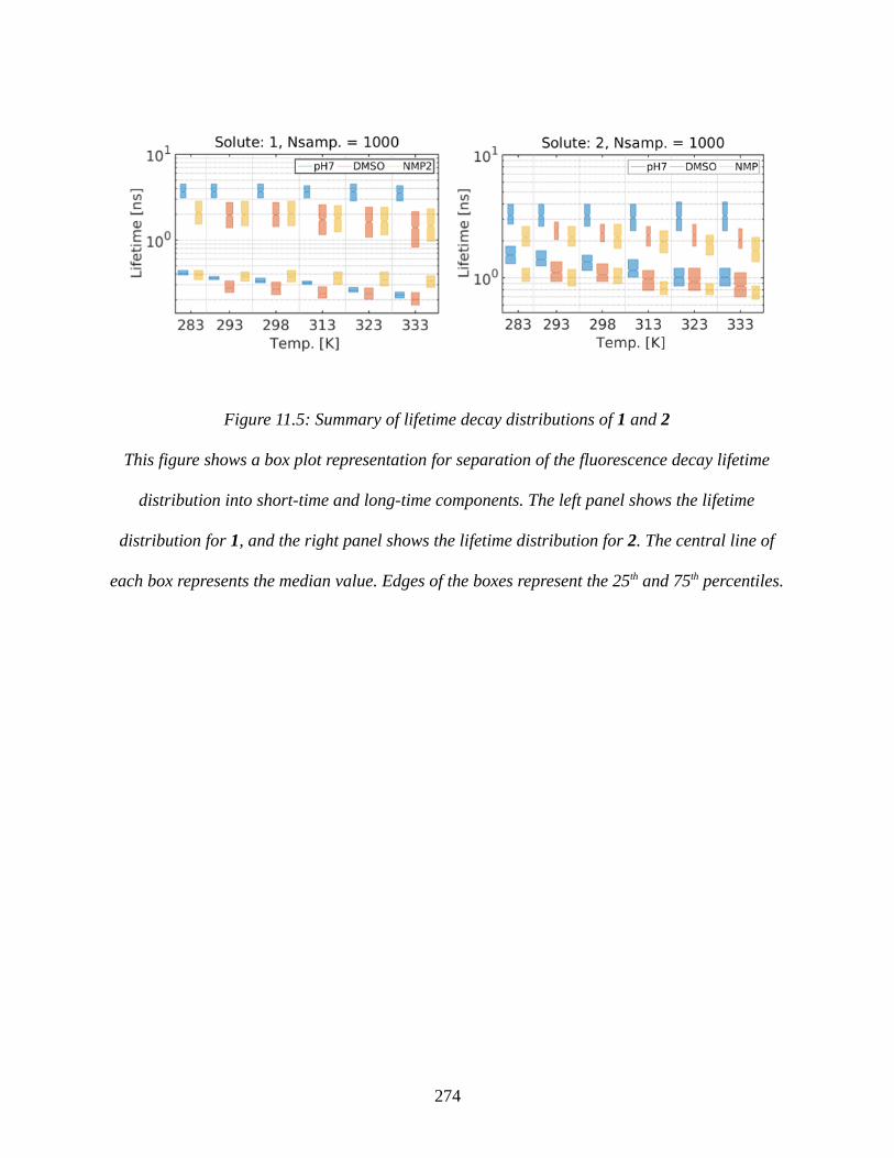
274
Figure 11.5: Summary of lifetime decay distributions of 1 and 2
This figure shows a box plot representation for separation of the fluorescence decay lifetime
distribution into short-time and long-time components. The left panel shows the lifetime
distribution for 1, and the right panel shows the lifetime distribution for 2. The central line of
each box represents the median value. Edges of the boxes represent the 25th and 75th percentiles.

The temperature dependence of the forward and backward electron transfer rate constants
are shown in Equation 11.6. Because of the double exponential character of the excited state
decay law, it is possible to determine the reaction Gibbs energy directly from the rate constants
as described in Equation 11.7; see Table 4. The free energy of the LE → CS reaction, ΔrG , is
given by
Figure S5 plots the reaction free energy as a function of temperature and shows that the
dependence on temperature is very weak. In fact, the free energies observed over the temperature
range in each solvent are smaller than the spread in the k+ and k- caused by the inherent width of
the lifetime distributions. In Table 4 ΔrG values for each solvent are reported at T = 298 K.
275
ΔrG=−RT ln( k for
kback)
Equation 11.7
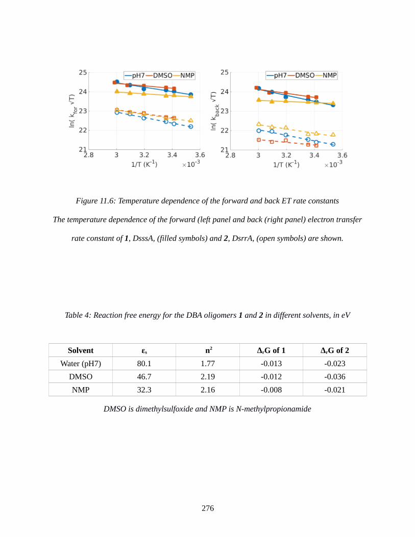
276
Figure 11.6: Temperature dependence of the forward and back ET rate constants
The temperature dependence of the forward (left panel and back (right panel) electron transfer
rate constant of 1, DsssA, (filled symbols) and 2, DsrrA, (open symbols) are shown.
Table 4: Reaction free energy for the DBA oligomers 1 and 2 in different solvents, in eV
Solvent εs n2 ΔrG of 1 ΔrG of 2
Water (pH7) 80.1 1.77 -0.013 -0.023
DMSO 46.7 2.19 -0.012 -0.036
NMP 32.3 2.16 -0.008 -0.021
DMSO is dimethylsulfoxide and NMP is N-methylpropionamide
11.3.3 Electron Transfer Rate Analysis
The electron transfer rate constant analysis used a semi-classical version of the Marcus
expression.[1; 15; 18; 40; 45] For a single effective quantum mode, the rate constant
kET can be written as
where kB is the Boltzmann’s constant, |V| is the electronic coupling matrix element, ΔrG is the
reaction free-energy, λs is the outer-sphere or solvent reorganization energy, ν is the frequency of
the effective quantized vibrational mode, and S is the Huang-Rhys factor given as the ratio of the
inner-sphere reorganization energy, λv, to the quantized mode energy spacing, λv /hν . The hν
term refers to the energy of a single effective quantized mode associated with the electron
transfer reaction; it is specific to the solute vibrational manifold and is not very sensitive to
solvent and temperature. Thus, hν and λv are fixed at values appropriate for the donor and
acceptor, and they are not changed as the bridge, solvent, and temperature change.
The lines of best fit in Figure 11.6 represent fits to the semi-classical electron-transfer
rate equation (Equation 11.8). The data reveal that the forward (and backward) electron transfer
rate for 1 in the three solvents are significantly higher than that of 2 in the same three solvents.
277
k ET =2 πℏ|V|2
1
√4π λs k B T∑n=0
∞
e−S( Sn
n!)exp(−(λ s+Δr G+nh ν)2
4λ s k BT )
Equation 11.8

Given that 1 and 2 have the same donor and acceptor units and the two bridges are diastereomers
of one another, the difference in the electron transfer rate occurs because of the different spatial
positioning of the donor and acceptor with respect to each other. In this analysis, 1400 cm-1 was
used as the value for the single effective quantized mode and 0.30 eV for the inner-sphere
reorganization energy. These values are the same as those used in previous work on donor-
bridge-acceptor systems having the same donor and a similar acceptor group; note that this
frequency value is typical of that for carbon-carbon stretching frequencies in aromatic ring
systems.[1; 8; 20] While roughly the same values for hν and λv were assumed as in
Chakrabarti, et. al.[8], these values may have some variation because the pyrene moiety was
modified in this set of experiments. Although an error in the internal reorganization energy
affects the absolute magnitude of the electronic coupling that is extracted from fits to the
semiclassical equation (Equation 11.8), the relative values of the coupling for the same solute in
different solvents is not sensitive to the choice of internal reorganization energy.[20] Note that
the redox potential of the pyrene is changed by the amide modification, and it is expected to
decrease the reduction potential of pyrene.[10; 19]
278
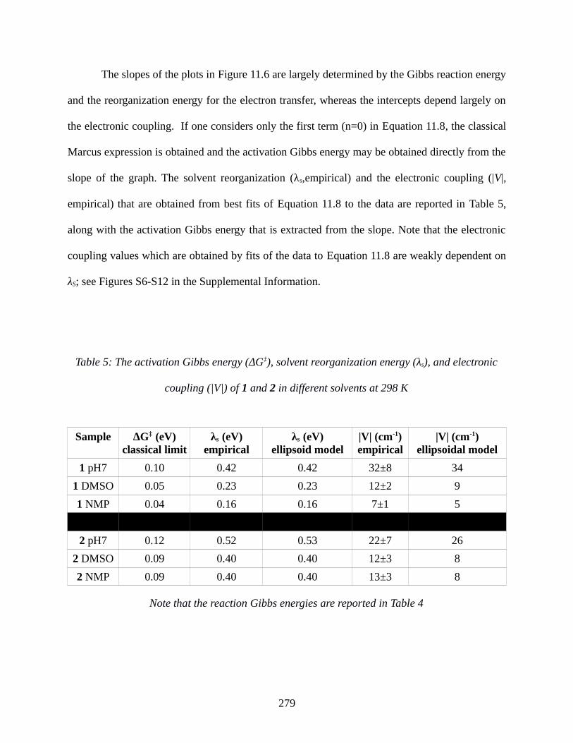
The slopes of the plots in Figure 11.6 are largely determined by the Gibbs reaction energy
and the reorganization energy for the electron transfer, whereas the intercepts depend largely on
the electronic coupling. If one considers only the first term (n=0) in Equation 11.8, the classical
Marcus expression is obtained and the activation Gibbs energy may be obtained directly from the
slope of the graph. The solvent reorganization (λs,empirical) and the electronic coupling (|V|,
empirical) that are obtained from best fits of Equation 11.8 to the data are reported in Table 5,
along with the activation Gibbs energy that is extracted from the slope. Note that the electronic
coupling values which are obtained by fits of the data to Equation 11.8 are weakly dependent on
λS; see Figures S6-S12 in the Supplemental Information.
279
Table 5: The activation Gibbs energy (ΔG‡), solvent reorganization energy (λs), and electronic
coupling (|V|) of 1 and 2 in different solvents at 298 K
Sample ΔG‡ (eV)classical limit
λs (eV)empirical
λs (eV)ellipsoid model
|V| (cm-1)empirical
|V| (cm-1)ellipsoidal model
1 pH7 0.10 0.42 0.42 32±8 34
1 DMSO 0.05 0.23 0.23 12±2 9
1 NMP 0.04 0.16 0.16 7±1 5
2 pH7 0.12 0.52 0.53 22±7 26
2 DMSO 0.09 0.40 0.40 12±3 8
2 NMP 0.09 0.40 0.40 13±3 8
Note that the reaction Gibbs energies are reported in Table 4
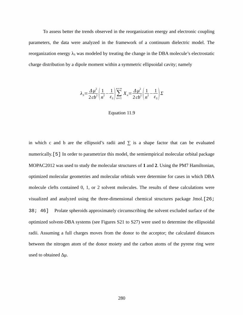
To assess better the trends observed in the reorganization energy and electronic coupling
parameters, the data were analyzed in the framework of a continuum dielectric model. The
reorganization energy λS was modeled by treating the change in the DBA molecule’s electrostatic
charge distribution by a dipole moment within a symmetric ellipsoidal cavity; namely
in which c and b are the ellipsoid’s radii and ∑ is a shape factor that can be evaluated
numerically.[5] In order to parametrize this model, the semiempirical molecular orbital package
MOPAC2012 was used to study the molecular structures of 1 and 2. Using the PM7 Hamiltonian,
optimized molecular geometries and molecular orbitals were determine for cases in which DBA
molecule clefts contained 0, 1, or 2 solvent molecules. The results of these calculations were
visualized and analyzed using the three-dimensional chemical structures package Jmol.[26;
38; 46] Prolate spheroids approximately circumscribing the solvent excluded surface of the
optimized solvent-DBA systems (see Figures S21 to S27) were used to determine the ellipsoidal
radii. Assuming a full charges moves from the donor to the acceptor; the calculated distances
between the nitrogen atom of the donor moiety and the carbon atoms of the pyrene ring were
used to obtained Δμ.
280
λS=Δ μ2
2 cb2 ( 1n2−
1εS)∑n=1
n=∞
Xn=Δ μ2
2 cb2 ( 1n2−
1εS)Σ
Equation 11.9
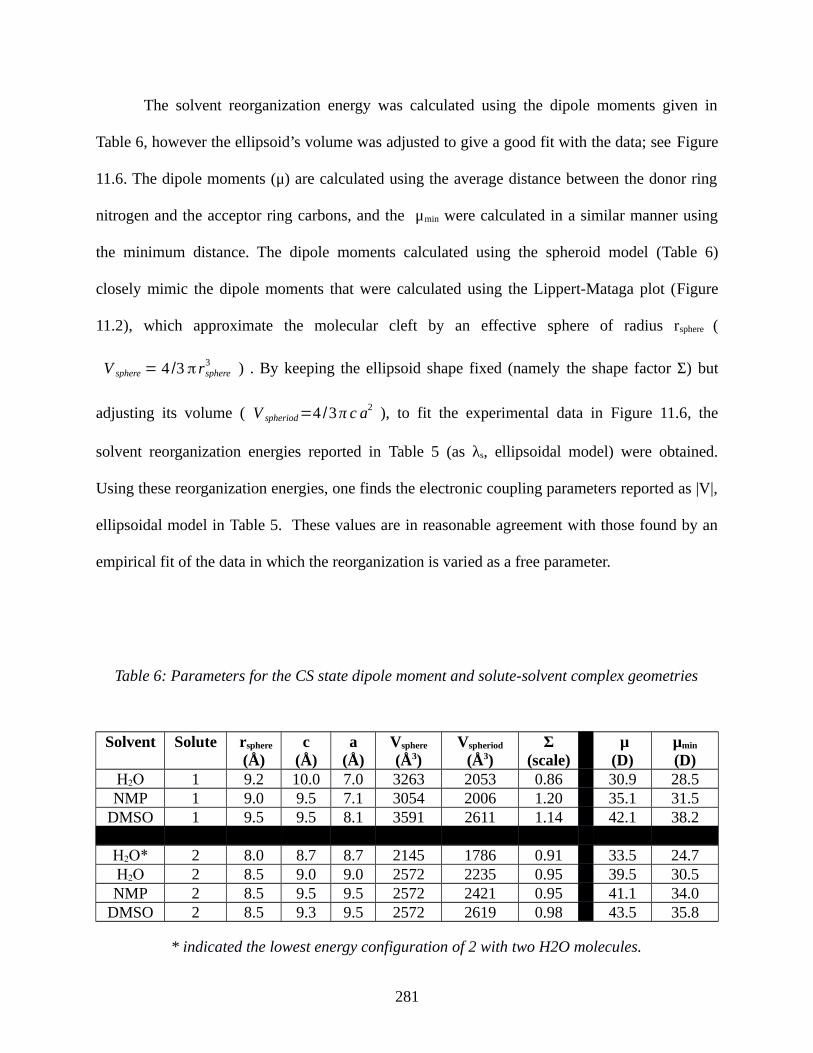
The solvent reorganization energy was calculated using the dipole moments given in
Table 6, however the ellipsoid’s volume was adjusted to give a good fit with the data; see Figure
11.6. The dipole moments (μ) are calculated using the average distance between the donor ring
nitrogen and the acceptor ring carbons, and the μmin were calculated in a similar manner using
the minimum distance. The dipole moments calculated using the spheroid model (Table 6)
closely mimic the dipole moments that were calculated using the Lippert-Mataga plot (Figure
11.2), which approximate the molecular cleft by an effective sphere of radius rsphere (
V sphere = 4 /3 π rsphere3 ) . By keeping the ellipsoid shape fixed (namely the shape factor Σ) but
adjusting its volume ( V spheriod=4 /3π c a2 ), to fit the experimental data in Figure 11.6, the
solvent reorganization energies reported in Table 5 (as λs, ellipsoidal model) were obtained.
Using these reorganization energies, one finds the electronic coupling parameters reported as |V|,
ellipsoidal model in Table 5. These values are in reasonable agreement with those found by an
empirical fit of the data in which the reorganization is varied as a free parameter.
281
Table 6: Parameters for the CS state dipole moment and solute-solvent complex geometries
Solvent Solute rsphere
(Å)c
(Å)a
(Å)Vsphere
(Å3)Vspheriod
(Å3)Σ
(scale) μ
(D)μmin
(D)H2O 1 9.2 10.0 7.0 3263 2053 0.86 30.9 28.5NMP 1 9.0 9.5 7.1 3054 2006 1.20 35.1 31.5
DMSO 1 9.5 9.5 8.1 3591 2611 1.14 42.1 38.2
H2O* 2 8.0 8.7 8.7 2145 1786 0.91 33.5 24.7H2O 2 8.5 9.0 9.0 2572 2235 0.95 39.5 30.5NMP 2 8.5 9.5 9.5 2572 2421 0.95 41.1 34.0
DMSO 2 8.5 9.3 9.5 2572 2619 0.98 43.5 35.8
* indicated the lowest energy configuration of 2 with two H2O molecules.
Note that the scaling factor Σ for 1 in water is quite different from the scaling factor for
solute 1 in the other solvents (NMP and DMSO) and the “loose-cleft” forming systems, 2, in all
solvents. Water has the most interaction with the cleft, as suggested by the electron transfer data.
The solvent water facilitates electron transfer most efficiently in DBA solute 1, as indicated by
the large coupling parameter (see Table 5). Because water has the most interaction with the cleft,
particularly in 1, the scaling factor is less predictable. In system 2 multiple waters can fit into the
cleft, thus an individual water molecule does not have as significant interaction with the cleft.
11.4 DISCUSSION
These studies build on the earlier work of Chakrabarti et. al.,[8] by investigating an amide
substituted acceptor unit which can interact favorably with a hydrogen bonding solvent. The
donor unit used in both systems is the same. Although amide modification has a small effect on
the overall molecular volume, the cleft size changes somewhat with the solvent type, vide infra.
In addition, amide modification causes a red-shift in the absorption spectrum, decreases the
excited stated lifetime, and alters the energetics of the electron transfer reaction. In particular, the
ΔrG for the amide modified pyrene system is significantly smaller than that of the unmodified
pyrene system. This decrease in the ΔrG facilitates the equilibrium between the locally excited
state and the charge separated state and allows for a significant charge transfer emission to be
observed; in contrast to the unsubstituted case of Chakrabarti et. al. for which no charge transfer
emission could be seen.
282
The time resolved fluorescence of 1 and 2 was collected at the red edge of the emission
spectrum because it displayed a double exponential decay law. The decay law at more blue
emission wavelengths had a third component, which was traced to a direct interaction between
the solubilizing lysine groups on the bridge and the acceptor (see Supplemental Information).
The red edge emission arises from both the locally excited state and the charge separated state;
however this could be modeled quantitatively in the kinetic scheme for the reaction. This kinetic
scheme, shown in Figure 11.3, was used to extract the ΔrG for the reaction directly from the
kinetic data.
The ΔrG values for 1 and 2 are significantly different from the ΔrG that were used to
model the electron transfer for the corresponding donor-bridge structure and unsubstituted
pyrene acceptor, which were reported to be -0.66 eV and -0.54 eV in water.[8] Most of the
shift in the ΔrG arises from the amide functionality that has been added to the pyrene. This fact
was confirmed by performing ultraviolet photoelectron spectra (UPS) of the bridge-acceptor
molecules (see Figure S14), and it is supported by literature data on similar systems.[10; 20]
The ΔrG for 1 and 2 are the same within experimental error; in contrast the ‘tight’ and ‘loose’
cleft molecules reported on by Chakrabarti [8] differed by 0.1 eV. These facts support a view
that the amide modification changes both the intrinsic reduction potential of the acceptor and the
solvation of the acceptor, as compared to the unsubstituted pyrene system. The amide
substitution may open the cleft and reduce the hydrophobic interaction between the donor and
acceptor; potentially, allowing it to incorporate multiple solvent molecules.
This view of the cleft is consistent with the difference in solvent reorganization energy
found for this system as compared to that reported by Chakrabarti [8] for the unsubstituted
case. In the unsubstituted case, the π-π and hydrophobic interactions control the solvation
283
environment of the cleft, so that a large solvent reorganization occurs upon formation of the
charge separated state. For DBA systems 1 and 2 the cleft environment is already somewhat
polar. Note that the reaction Gibbs energy and reorganization parameters in the semi-classical
equation are highly coupled, and Chakarabarti [8] was unable to experimentally determine ΔrG
in the donor-bridge-acceptor system; hence the absolute difference in the reorganization energies
should not be interpreted too strictly.
In order to examine the features of the molecular cleft more quantitatively, quantum
chemistry (PM7) simulations of 1 and 2 with solvent were performed. These calculations
showed that the cleft in 1 and 2 was able to adapt to the size of the solvent molecules studied
(water, DMSO, and NMP). For the case of DMSO and NMP (see SI) only one solvent molecule
was able to fit in the cleft of 2, and similarly only one solvent molecule could fit in the cleft of 1.
The contact surfaces and the donor to acceptor distances for these cleft/solvent systems were
similar, and this finding is compatible with the similar reorganization energies and electronic
couplings reported for these systems.
284
285
Figure 11.7: HOMO and LUMO molecular orbitals of two DBA molecules
Frontier HOMO(orange/grey) and LUMO(yellow/green) molecular orbitals are shown for the
two DBA molecules with water. In panel A the entire DBA structure is displayed. Panel C shows
a plot of the distance between the nitrogen atom of the donor and the carbon atoms of the pyrene
ring at the optimized geometry. The expanded view in panels (B) and (D) the lysine moieties
have been removed to facilitate observation of the DBA cleft region. The interaction surface of
the solvent molecules is shown, as well.
Simulations of 1 and 2 with water solvent were performed for both one and two solvent
molecules in the cleft (see Figure 11.7 and SI). For both solutes the cleft could accommodate one
water molecule; however the loose cleft (2) had a better van der Waals contact with two water
molecules present than with one. Panel 7b shows the energy minimum for two water molecules
in the cleft of 2 and panel 7d shows the energy minimum for two water molecules in the cleft of
1. The tight cleft does not let the water molecules fill it, whereas the loose cleft does. Panel 7c
shows plots of the distance between the donor N atom and the different C atoms of the pyrene
acceptor for the tight cleft (1) with one and two water molecules and the loose cleft (2) with two
water molecules; note that the loose cleft with one water molecule had no clear energetic
minimum. Note that the tight cleft’s distances change only slightly in accommodating more than
one water molecule, and that these distances range from 6 to 7 Å depending on ring location. In
contrast the loose cleft shows a broader range of distances (5 to 9 Å) and it has some regions of
the ring closer to the donor N. These data underscore the different cleft geometries, yet are
consistent with the similar electronic couplings that are found for water. Namely, the electron
tunneling is controlled by distance and although the loose cleft has a small area of the acceptor
placed closer to the donor, most of it is farther from the donor than the distances for the tight
cleft. The calculations show that the contact interaction with the solvent controls the donor to
acceptor distance. Although 2 has a few 5Å contact interactions, its average contact distance is 7
Å; whereas molecule 1 has an average of 6.4 Å. The net result appears to be a similar coupling
for the two cases.
286
electronic coupling would be higher for the case of water than the other cases, in agreement with
the fits to the data; see Table 5. NMP and DMSO both facilitate electron transfer, however the
rate constant is smaller because the donor to acceptor distance is larger and hence it has a smaller
electronic coupling. Because the cleft spacings are similar for 1 and 2 with DMSO and NMP, the
electronic couplings are found to be similar. Thus, the ability of the cleft to accommodate
different sizes and numbers of solvent molecules gives rise to a behavior that is more rich than
that found for the strictly hydrophobic donor-acceptor system reported by Chakrabarti.[8]
11.5 CONCLUSION
The amide substitution on the pyrene in the donor-bridge-acceptor system changes both the
reaction Gibbs energy for the photoinduced electron transfer and the hydrophilicity of the
molecular cleft. The less negative ΔrG allows one to observe the charge separated emission,
under appropriate solvent conditions as compared to the system reported earlier for the
unsubstituted pyrene. The increased hydrophilicity of the cleft impacts its ability to
accommodate solvent and change the interaction between the donor (DMA) and acceptor
(pyrene). As with the earlier study for the unsubstituted pyrene acceptor, in which water was able
to lodge in the cleft and mediate the electron tunneling, the amide substituted pyrene forms a
cleft that can accommodate water molecules. In contrast to the earlier study, the cleft for 1 and 2
appears to be able to accommodate larger solvent molecules (and multiple water molecules).
This feature suggests that substitution of the pyrene ring might be used to tune the cleft’s
solvation characteristics and the size of the tunneling gap.
287

11.6 BIBLIOGRAPHY
[1] Barbara, P. F.; Meyer, T. J. and Ratner, M. A. (1996). Contemporary issues in electron transfer research, The Journal of Physical Chemistry 100 : 13148-13168.
[2] Beratan, D. N.; Skourtis, S. S.; Balabin, I. A.; Balaeff, A.; Keinan, S.; Venkatramani, R. and Xiao, D. (2009). Steering electrons on moving pathways, Accounts of chemical research 42 : 1669-1678.
[3] Bingo l, B.; Durrell, A. C.; Keller, G. E.; Palmer, J. H.; Grubbs, R. H. and Gray, H. B. (2012). Electron Transfer Triggered by Optical Excitation of Phenothiazine-tris (meta-phenylene-ethynylene)-(tricarbonyl)(bpy)(py) rhenium (I), The Journal of Physical Chemistry B 117 : 4177-4182.
[4] Borsarelli, C. D.; Cosa, J. J. and Previtali, C. M. (1992). Exciplex formation between pyrene derivatives and N, N-dimethylaniline in aerosol OT reversed micelles, Langmuir 8 : 1070-1075.
[5] Brunschwig, B. S.; Ehrenson, S. and Sutin, N. (1986). Solvent reorganization in optical and thermal electron-transfer processes, J. Phys. Chem. 90 : 3657–3668.
[6] Chakrabarti, S.; Liu, M.; Waldeck, D. H.; Oliver, A. M. and Paddon-Row, M. N. (2007). Competing electron-transfer pathways in hydrocarbon frameworks: Short-circuiting through-bond coupling by nonbonded contacts in rigid U-shaped norbornylogous systems containing a cavity-bound aromatic pendant group, Journal of the American Chemical Society 129 : 3247-3256.
[7] Chakrabarti, S.; Liu, M.; Waldeck, D. H.; Oliver, A. M. and Paddon-Row, M. N. (2009). Solvent dynamical effects on electron transfer in U-shaped donor-bridge-acceptor molecules, The Journal of Physical Chemistry A 113 : 1040-1048.
[8] Chakrabarti, S.; Parker, M. F.; Morgan, C. W.; Schafmeister, C. E. and Waldeck, D. H. (2009). Experimental evidence for water mediated electron transfer through bis-amino acid donor- bridge- acceptor oligomers, Journal of the American Chemical Society 131 : 2044-2045.
[9] Douglas, K.; Bichenkova, E. and Sardarian, A. (2003). US Patent US 20030108892 A1.
[10] Feldman, K. S.; Hester, D. K. and Golbeck, J. H. (2007). A relationship between amide hydrogen bond strength and quinone reduction potential: Implications for photosystem I and bacterial reaction center quinone function, Bioorganic & medicinal chemistry letters 17 : 4891-4894.
288

[11] Gilbert, A. and Baggott, J. E., 1991. Essentials of molecular photochemistry. Wiley-Blackwel, .
[12] Gilbert, M. and Albinsson, B. (2015). Photoinduced charge and energy transfer in molecular wires, Chemical Society Reviews 44 : 845-862.
[13] Gordon, M. and Ware, W., 1975. The Exciplex. Academic Press Inc., .
[14] Gould, I. R.; Ege, D.; Moser, J. E. and Farid, S. (1990). Efficiencies of photoinduced electron-transfer reactions: role of the Marcus inverted region in return electron transfer within geminate radical-ion pairs, Journal of the American Chemical Society 112 : 4290-4301.
[15] Gratzel, M., 1989. Heterogeneous photochemical electron transfer. CRC Press, .
[16] Gu, Y.; Kumar, K.; Lin, Z.; Read, I.; Zimmt, M. and Waldeck, D. (1997). Studies into the character of electronic coupling in electron transfer reactions, Journal of Photochemistry and Photobiology A: Chemistry 105 : 189-196.
[17] Haedler, A. T.; Misslitz, H.; Buehlmeyer, C.; Albuquerque, R. Q.; Köhler, A. and Schmidt, H.-W. (2013). Controlling the pi-stacking behavior of pyrene derivatives: Influence of H-bonding and steric effects in different states of aggregation, ChemPhysChem 14 : 1818-1829.
[18] Jortner, J. and Bixon, M.Prigogine, I. & Rice, S. A. (Ed.), 1999. Electron Transfer -- From Isolated Molecules to Biomolecules, Part 1 and Part 2. John Wiley & Sons Inc, .
[19] Kerr, C. E.; Mitchell, C. D.; Headrick, J.; Eaton, B. E. and Netzel, T. L. (2000). Synthesis and photophysics of a 1-Pyrenyl substituted 2'-Deoxyuridine-5-Carboxamide nucleoside: Electron transfer products as CIS INDO/S excited states, The Journal of Physical Chemistry B 104 : 1637-1650.
[20] Kumar, K.; Kurnikov, I. V.; Beratan, D. N.; Waldeck, D. H. and Zimmt, M. B. (1998). Use of modern electron transfer theories to determine electronic coupling matrix elements in intramolecular systems, The Journal of Physical Chemistry A 102 : 5529-5541.
[21] Kuzmin, M. G. (1993). Exciplex mechanism of the fluorescence quenching in polar media, Pure and applied chemistry 65 : 1653-1658.
[22] Lakowicz, J. R., 2007. Principles of Fluorescence Spectroscopy. Springer US, .
[23] These radii were calculated using the circumscribed sphere (Figures S21 and S24).
[24] Lewis, F. D. (1979). Formation and reactions of stilbene exciplexes, Accounts of Chemical Research 12 : 152-158.
[25] Liu, M.; Ito, N.; Maroncelli, M.; Waldeck, D. H.; Oliver, A. M. and Paddon-Row, M. N. (2005). Solvent friction effect on intramolecular electron transfer, Journal of the American Chemical Society 127 : 17867-17876.
289
[26] Maia, J. D. C.; Carvalho, G. A. U.; Mangueira, C. P.; Santana, S. R.; Cabral, L. A. F. and Rocha, G. B. (2012). GPU linear algebra libraries and GPGPU programming for accelerating MOPAC semiempirical quantum chemistry calculations, J. Chem. Theory Comput. 8 : 3072-3081.
[27] Marcus, R. (1989). Relation between charge transfer absorption and fluorescence spectra and the inverted region, The Journal of Physical Chemistry 93 : 3078-3086.
[28] Mataga, N. and Kubota, T., 1970. Molecular Interaction and Electronic Spectra. Marcel Dekker Inc., .
[29] McGuinness, C. D.; Nishimura, M. K.; Keszenman-Pereyra, D.; Dickinson, P.; Campbell, C. J.; Bachmann, T. T.; Ghazal, P. and Crain, J. (2010). Detection of single nucleotide polymorphisms using a DNA Holliday junction nanoswitch – a high-throughput fluorescence lifetime assay, Molecular BioSystems 6 : 386-390.
[30] Nadeau, J. M.; Liu, M.; Waldeck, D. H. and Zimmt, M. B. (2003). Hole transfer in a C-shaped molecule: Conformational freedom versus solvent-mediated coupling, Journal of the American Chemical Society 125 : 15964-15973.
[31] Napper, A. M.; Head, N. J.; Oliver, A. M.; Shephard, M. J.; Paddon-Row, M. N.; Read, I. and Waldeck, D. H. (2002). Use of U-shaped donor-bridge-acceptor molecules to study electron tunneling through nonbonded contacts, Journal of the American Chemical Society 124 : 10171-10181.
[32] Natali, M.; Campagna, S. and Scandola, F. (2014). Photoinduced electron transfer across molecular bridges: electron-and hole-transfer superexchange pathways, Chemical Society Reviews 43 : 4005-4018.
[33] Okada, T.; Fujita, T.; Kubota, M.; Masaki, S.; Mataga, N.; Ide, R.; Sakata, Y. and Misumi, S. (1972). Intramolecular electron donor-acceptor interactions in the excited state of (anthracene)-(CH 2) n-(N, N-dimethylaniline) systems, Chemical Physics Letters 14 : 563-568.
[34] Paddon-Row, M. N. (2003). Orbital interactions and long-range electron transfer, Advances in Physical Organic Chemistry 38 : 1-85.
[35] Read, I.; Napper, A.; Kaplan, R.; Zimmt, M. and Waldeck, D. (1999). Solvent-mediated electronic coupling: The role of solvent placement, Journal of the American Chemical Society 121 : 10976-10986.
[36] Reis e Sousa, A.; Castanheira, E.; Fedorov, A. and Martinho, J. (1998). Polystyrene cyclization using pyrene excimer formation. Effect of geminate pairs in good solvents, The Journal of Physical Chemistry A 102 : 6406-6411.
[37] Skourtis, S. S.; Waldeck, D. H. and Beratan, D. N. (2010). Fluctuations in biological and bioinspired electron-transfer reactions, Annual review of physical chemistry 61 : 461.
[38] MOPAC2012, Version 15.229L, Stewart James, J. P., Web: HTTP://OpenMOPAC.net
290
[39] Van Haver, P.; Helsen, N.; Depaemelaere, S.; Van der Auweraer, M. and De Schryver, F. (1991). The influence of solvent polarity of the nonradiative decay of exciplexes, Journal of the American Chemical Society 113 : 6849-6857.
[40] Van Voorhis, T.; Kowalczyk, T.; Kaduk, B.; Wang, L.-P.; Cheng, C.-L. and Wu, Q. (2010). The diabatic picture of electron transfer, reaction barriers, and molecular dynamics, Annual review of physical chemistry 61 : 149-170.
[41] Verhoeven, J.; Scherer, T. and Willemse, R. (1993). Solvent effects on the structure of fluorescent'exciplexes' in rigidly-, flexibly-, and nonbridged donor-acceptor systems, Pure and applied chemistry 65 : 1717-1722.
[42] Verhoeven, J. W. (1990). Electron transport via saturated hydrocarbon bridges:'exciplex'emission from flexible, rigid and semiflexible bichromophores, Pure and Applied Chemistry 62 : 1585-1596.
[43] Weiss, E. A.; Wasielewski, M. R. and Ratner, M. A. (2005). Molecules as wires: Molecule-assisted movement of charge and energy, Top. Curr. Chem 257 : 103-133.
[44] Yin, X.; Kong, J.; De Leon, A.; Li, Y.; Ma, Z.; Wierzbinski, E.; Achim, C. and Waldeck, D. H. (2014). Luminescence quenching by photoinduced charge transfer between metal complexes in peptide nucleic acids, The Journal of Physical Chemistry B 118 : 9037-9045.
[45] Zimmt, M. and Waldeck, D. (2003). Exposing solvent's roles in electron transfer reactions: Tunneling pathway and solvation, The Journal of Physical Chemistry A 107 : 3580-3597.
[46] JSmol: an open-source HTML5 viewer for chemical structures in 3D., Web: http://wiki.jmol.org/index.php/JSmol
291

12.0 CONCLUSIONS
A brief description of the conclusions of the studies contained within this thesis are described
below.
Conclusions of Part I: Scanning Probe Microscopy:
In Chapter 3, we demonstrated ANSOM images of a nanoslit aperture containing
interference fringes, which result from superposition of the average detected wavevector and
components of the field scattered by the nanoslit. Analysis confirms that such a slit generates two
scattered orders launched perpendicular to the slit. Furthermore, fringe patterns can be controlled
by changing the orientation of the slit, and thus, the direction of the two scattered orders with
respect to the detector or vice versa. The model originally developed by Aubert et al. was
extended to account for the two scattered orders present in our system. The resulting calculated
fields agreed well with the ANSOM data in several different detector-slit orientations.
Additionally, probe geometry and probe position relative to the slit strongly affect the
magnitude of self-homodyning fields exhibited in ANSOM images. For a single slit aperture,
sources of homodyning fields include a propagating field transmitted through the slit and
reflected by the probe base and/or cantilever body. Sensitivity of self-homodyne amplification to
probe geometry suggests that portions of the probe base and cantilever body scatter significant
transmitted optical fields.
292

In Chapter 4 the bending modulus of individual multiwall boron nitride nanotubes
(MWBNNTs) was measured via AFM bending experiments. Boundary conditions for the beam-
bending model were determined by using a force mapping technique. MWBNNTs were found to
have excellent mechanical properties with an average bending modulus of 760 ± 30 GPa, which
is consistent with the theoretically predicted value for BNNTs. Shear effects were found to be
non-negligible, and the Young’s modulus and shear modulus were determined to be 1800 ± 300
and 7 ± 1 GPa, respectively. The experimental geometry and the dimensions of the nanotubes
were not major contributing factors to the shear effects; rather, it is likely that interwall shearing
occurred between crystalline and faceted cylindrical helices in these MWBNNTs.
Conclusions of Part II: Studies of Photonic Crystals
In Chapter 6 we developed a simple, straightforward method to form non close-packed
ultra-highly-ordered, face centered cubic (fcc) direct and inverse opal silica photonic crystals,
which allowed us to independently control the photonic crystal periodicity and size of the basis
of the fcc unit cell. We selected the fcc lattice constant by defining the particle number density of
this electrostatically self assembled structure. Thus, we independently control the spacing
between particles. The particle diameter used determines the wall spacing of the inverse opal
photonic crystal and determines the shape of the photonic crystal dielectric constant modulation.
This allows us to optimize the diffraction of our photonic crystal structures.
These fcc photonic crystals simply and spontaneously self assemble due to their soft
electrostatic repulsion potentials. They showed ordering as good or possibly better than close-
packed photonic crystals formed by convective assembly. We showed that colloidal particle size
polydispersity has less impact on photonic crystal electrostatic ordering than occured for
ordering of close-packed crystals. Point defect induced crystal strains in electrostatically
293

stabilized CCA anneal within approximately two particle layers. We also showed that charge
polydispersity has only a small impact on crystal ordering and that the strains due to defect
particles of different charge also anneal out over approximately two particle layers.
In Chapter 7 we developed a novel, simple, and efficient approach to rapidly fabricate
large-area 2-D particle arrays on water surfaces. These arrays can easily be transferred onto
various substrates and functionalized for chemical-sensing applications. We demonstrated that
the ordering of 2-D arrays decreases with the particle size.
Conclusions of Part III: Spectroscopy Studies.
In Chapter 9 we demonstrated that electron transfer and photoluminescence quenching in
cadmium selenide / cadmium telluride NP assemblies can be controlled through the interparticle
distance, energetics, electric field created by the surface capping group, and particle size. Time-
resolved studies indicated that the electron transfer process may involve surface-localized states.
The inhibition of electron transfer by the interparticle electric field was significant and may
provide an avenue for inhibiting back electron transfer. These findings should be useful for
understanding and controlling charge transfer in nanocrystal-based solar cells.
In Chapter 10 efficient sensitization was observed for both the ZnS/Tb3+ and the
ZnS/Eu3+ systems. The ZnS/Tb3+ nanoparticles appear to be more efficient lanthanide-based
emitters, with lanthanide-centered quantum yield values for ZnS/Tb3+ and ZnS/Eu3+ being 0.05
± 0.01 and 0.000 13 ± 0.000 04, respectively. ZnS nanoparticles acted as an antenna to sensitize
the lanthanide luminescence in these systems. Moreover, the absence of observable sharp bands
in the excitation spectra indicated that direct excitation of lanthanides has a negligible
contribution to the overall sensitization mechanism.
294
The mechanism of lanthanide luminescence sensitization in II−VI semiconductor
materials can be rationalized by a semiempirical method proposed by Dorenbos and colleagues.
Energy level diagrams indicate that in ZnS, Tb3+ can act as a potential hole trap and provide a
dramatic increase in sensitization efficiency because its energy levels lie between the
nanoparticle band edges. The mechanism of Eu3+ luminescence sensitization on the other hand,
follows a different type of mechanism. In ZnS, Eu3+ can act as a potential electron trap; hence,
the sensitization can be achieved either by direct bandgap excitation or by a valence band to
Eu2+ transition.
In Chapter 11 the amide substitution on the pyrene in the donor-bridge-acceptor system
changed both the reaction Gibbs energy for the photoinduced electron transfer and the
hydrophilicity of the molecular cleft. The less negative ΔrG allows one to observe the charge
separated emission, under appropriate solvent conditions as compared to the system reported
earlier for the unsubstituted pyrene. The increased hydrophilicity of the cleft impacts its ability
to accommodate solvent and change the interaction between the donor (DMA) and acceptor
(pyrene). As with the earlier study for the unsubstituted pyrene acceptor in which water was able
to lodge in the cleft and mediate the electron tunneling, the amide substituted pyrene formed a
cleft that can accommodate water molecules. In contrast to the earlier study, the molecular clefts
appeared to be able to accommodate larger solvent molecules (and multiple water molecules).
This feature suggests that substitution of the pyrene ring might be used to tune the cleft’s
solvation characteristics and the size of the tunneling gap.
295