Embed Size (px)
Citation preview
7/30/2019 Chapter1_Integrated-Circuit Logic Family
http://slidepdf.com/reader/full/chapter1integrated-circuit-logic-family 1/52
BKTP.HCM
2010
dc e
Chapter 1INTERGRATED-CIRCUIT
LOGIC FAMILIES
Faculty of Computer Science and Engineering
Department of Computer Engineering
©2010, CE Department
7/30/2019 Chapter1_Integrated-Circuit Logic Family
http://slidepdf.com/reader/full/chapter1integrated-circuit-logic-family 2/52
2010
dc e
Outline
• Digital IC Terminology• TTL Logic Family
• MOS Technology• Open-Collector/Open-Drain Ouputs
• Tristate (Three-State) Logic Outputs
• IC Interfacing
©2010, CE Department 2
7/30/2019 Chapter1_Integrated-Circuit Logic Family
http://slidepdf.com/reader/full/chapter1integrated-circuit-logic-family 3/52
2010
dc e
3 ©2010, CE Department
Digital IC Terminology
7/30/2019 Chapter1_Integrated-Circuit Logic Family
http://slidepdf.com/reader/full/chapter1integrated-circuit-logic-family 4/52
2010
dc e
4 ©2010, CE Department
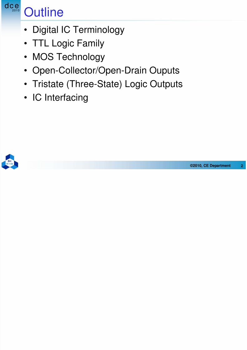
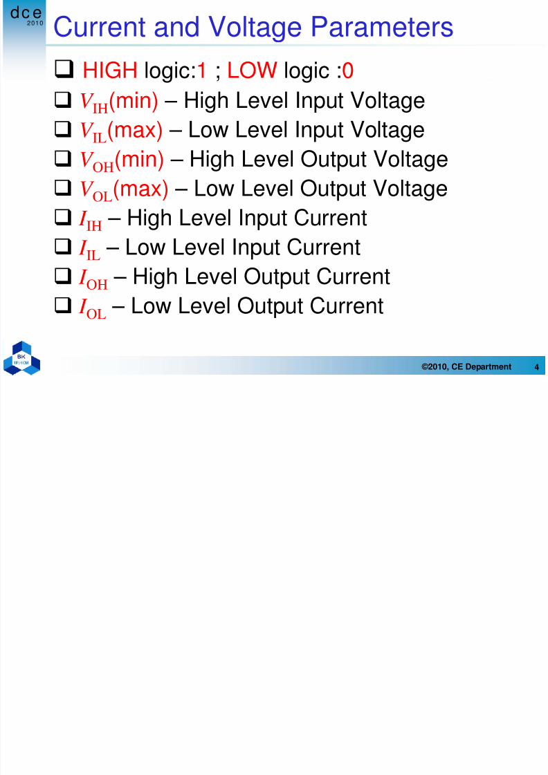
Current and Voltage Parameters
HIGH logic:1 ; LOW logic :0 V IH(min) – High Level Input Voltage
V IL(max) – Low Level Input Voltage V OH(min) – High Level Output Voltage
V OL(max) – Low Level Output Voltage
I IH – High Level Input Current
I IL – Low Level Input Current
I OH – High Level Output Current
I OL – Low Level Output Current
7/30/2019 Chapter1_Integrated-Circuit Logic Family
http://slidepdf.com/reader/full/chapter1integrated-circuit-logic-family 5/52
2010
dc e
5 ©2010, CE Department
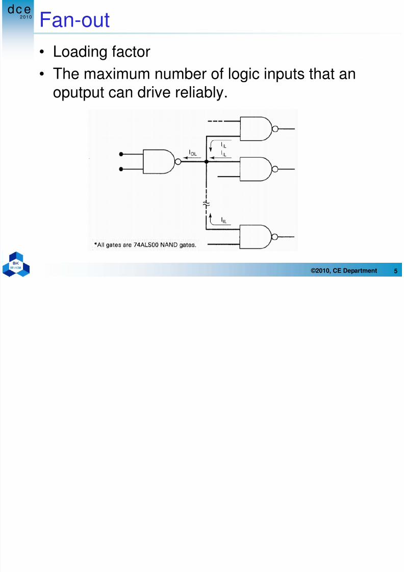
Fan-out
• Loading factor
• The maximum number of logic inputs that an
oputput can drive reliably.
7/30/2019 Chapter1_Integrated-Circuit Logic Family
http://slidepdf.com/reader/full/chapter1integrated-circuit-logic-family 6/52
2010
dc e
6 ©2010, CE Department
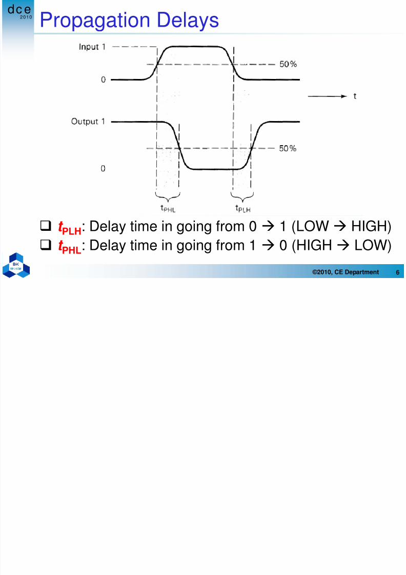
Propagation Delays
t PLH: Delay time in going from 0 Æ 1 (LOWÆ HIGH)
t PHL: Delay time in going from 1 Æ 0 (HIGHÆ LOW)
7/30/2019 Chapter1_Integrated-Circuit Logic Family
http://slidepdf.com/reader/full/chapter1integrated-circuit-logic-family 7/52
2010
dc e
7 ©2010, CE Department
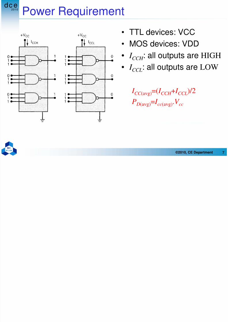
Power Requirement
• TTL devices: VCC
• MOS devices: VDD
• I CCH : all outputs are HIGH• I CCL: all outputs are LOW
I CC (avg)=( I CCH + I CCL)/2
P D(avg)= I cc(avg).V cc
7/30/2019 Chapter1_Integrated-Circuit Logic Family
http://slidepdf.com/reader/full/chapter1integrated-circuit-logic-family 8/52
2010
dc e
8 ©2010, CE Department
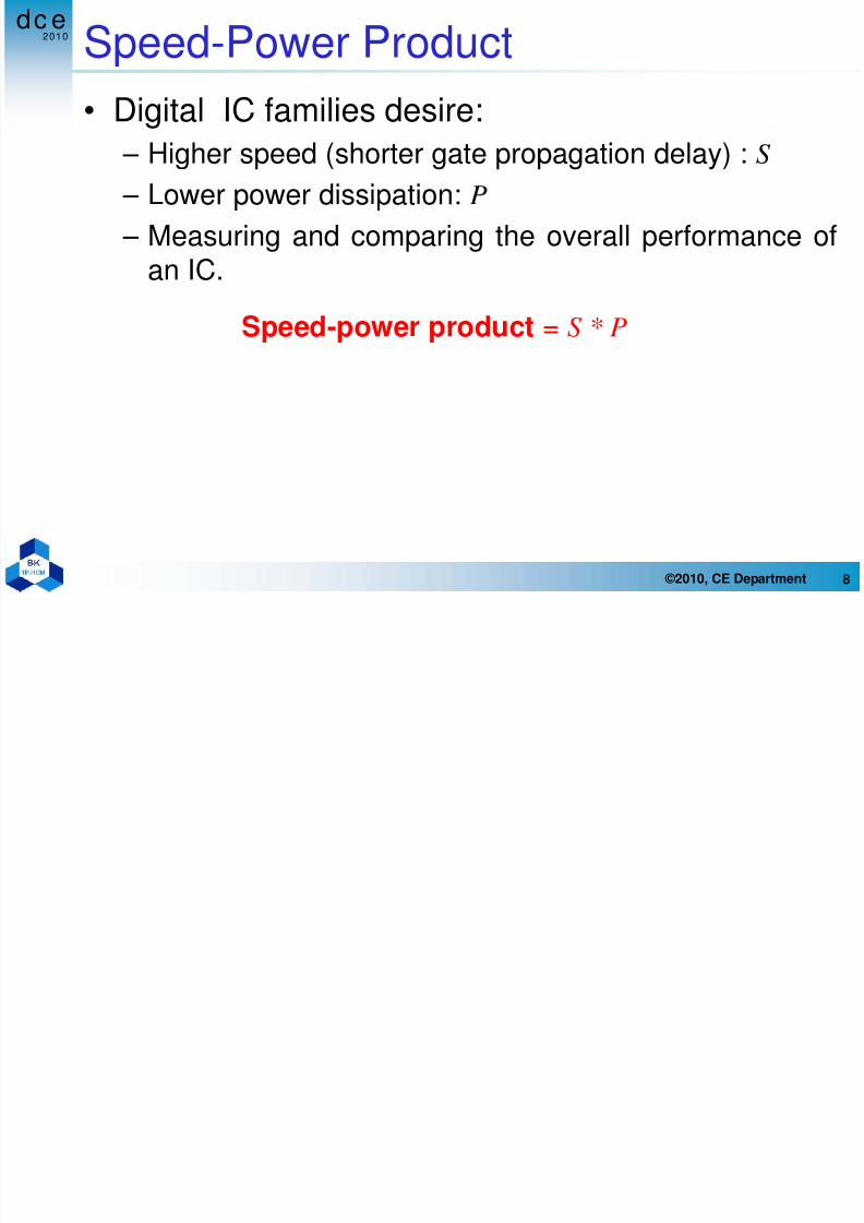
Speed-Power Product
• Digital IC families desire: – Higher speed (shorter gate propagation delay) : S
– Lower power dissipation: P – Measuring and comparing the overall performance of
an IC.
Speed-power product = S * P
d
7/30/2019 Chapter1_Integrated-Circuit Logic Family
http://slidepdf.com/reader/full/chapter1integrated-circuit-logic-family 9/52
2010
dc e
9 ©2010, CE Department
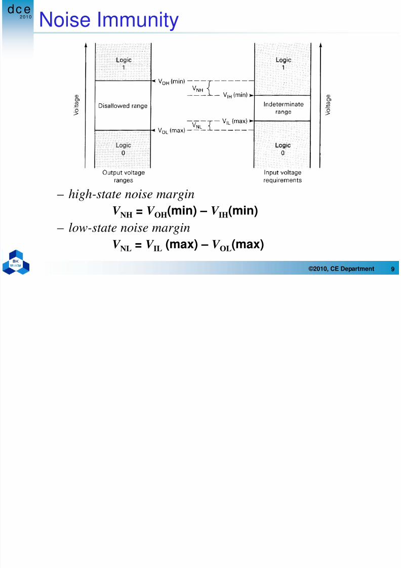
Noise Immunity
– high-state noise marginV NH
= V OH
(min) – V IH
(min)
– low-state noise margin
V NL = V IL (max) – V OL(max)
d
7/30/2019 Chapter1_Integrated-Circuit Logic Family
http://slidepdf.com/reader/full/chapter1integrated-circuit-logic-family 10/52
2010
dc e
10 ©2010, CE Department
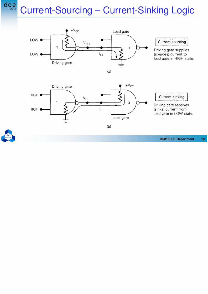
Current-Sourcing – Current-Sinking Logic
d
7/30/2019 Chapter1_Integrated-Circuit Logic Family
http://slidepdf.com/reader/full/chapter1integrated-circuit-logic-family 11/52
2010
dc e
11 ©2010, CE Department
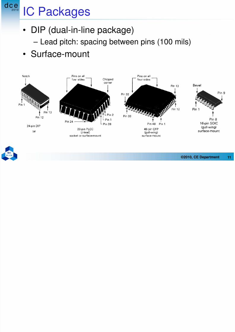
IC Packages
• DIP (dual-in-line package) – Lead pitch: spacing between pins (100 mils)
• Surface-mount
dc e
7/30/2019 Chapter1_Integrated-Circuit Logic Family
http://slidepdf.com/reader/full/chapter1integrated-circuit-logic-family 12/52
2010
dc e
12 ©2010, CE Department
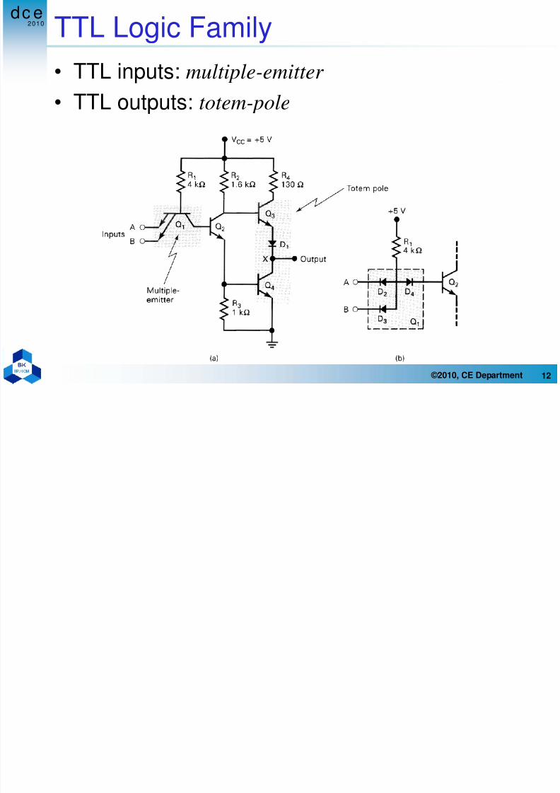
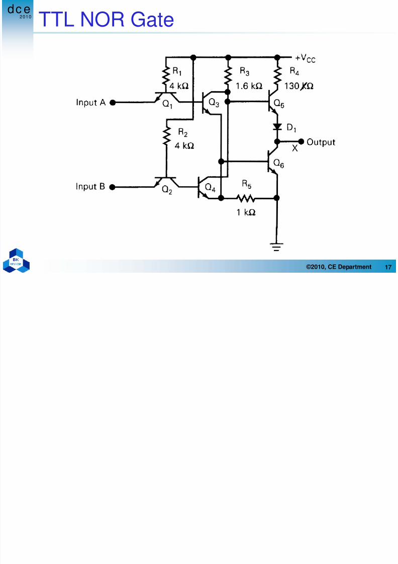
TTL Logic Family
• TTL inputs: multiple-emitter
• TTL outputs: totem-pole
7/30/2019 Chapter1_Integrated-Circuit Logic Family
http://slidepdf.com/reader/full/chapter1integrated-circuit-logic-family 13/52
dc e
7/30/2019 Chapter1_Integrated-Circuit Logic Family
http://slidepdf.com/reader/full/chapter1integrated-circuit-logic-family 14/52
2010
dc e
14 ©2010, CE Department
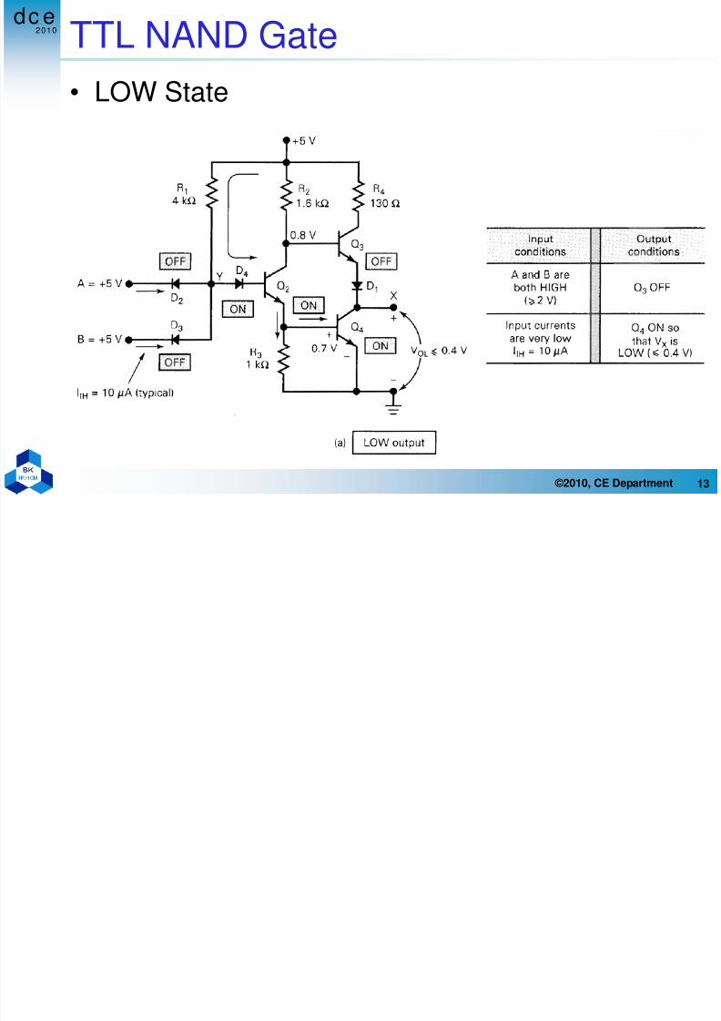
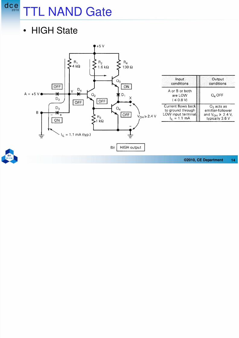
TTL NAND Gate
• HIGH State
dc e
7/30/2019 Chapter1_Integrated-Circuit Logic Family
http://slidepdf.com/reader/full/chapter1integrated-circuit-logic-family 15/52
2010
dc e
15 ©2010, CE Department
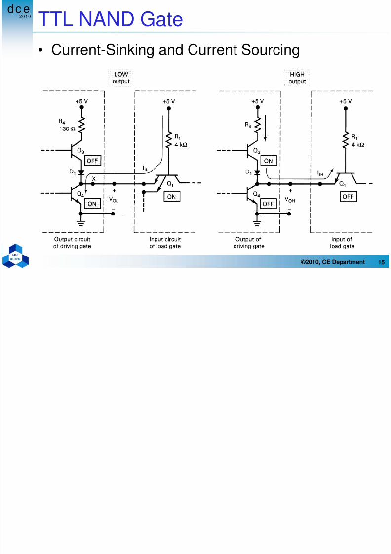
TTL NAND Gate
• Current-Sinking and Current Sourcing
dc e
7/30/2019 Chapter1_Integrated-Circuit Logic Family
http://slidepdf.com/reader/full/chapter1integrated-circuit-logic-family 16/52
2010
dc e
16 ©2010, CE Department
TTL NAND Gate
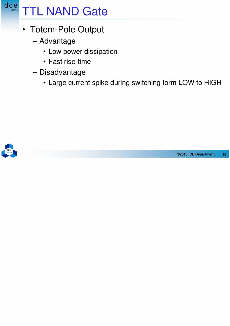
• Totem-Pole Output – Advantage
• Low power dissipation
• Fast rise-time
– Disadvantage
• Large current spike during switching form LOW to HIGH
7/30/2019 Chapter1_Integrated-Circuit Logic Family
http://slidepdf.com/reader/full/chapter1integrated-circuit-logic-family 17/52
dc e
7/30/2019 Chapter1_Integrated-Circuit Logic Family
http://slidepdf.com/reader/full/chapter1integrated-circuit-logic-family 18/52
2010
dc e
18 ©2010, CE Department
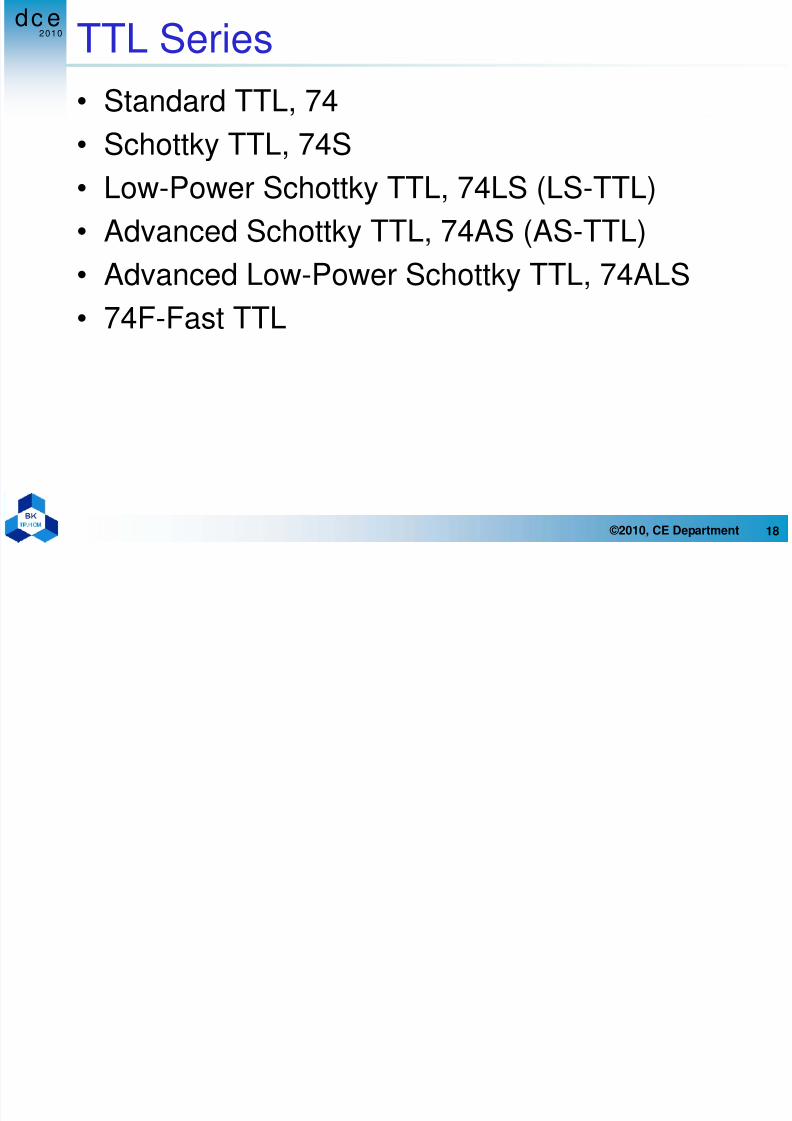
TTL Series
• Standard TTL, 74• Schottky TTL, 74S
• Low-Power Schottky TTL, 74LS (LS-TTL)• Advanced Schottky TTL, 74AS (AS-TTL)
• Advanced Low-Power Schottky TTL, 74ALS• 74F-Fast TTL
dc e
TTL D Sh
7/30/2019 Chapter1_Integrated-Circuit Logic Family
http://slidepdf.com/reader/full/chapter1integrated-circuit-logic-family 19/52
2010
dc e
19 ©2010, CE Department
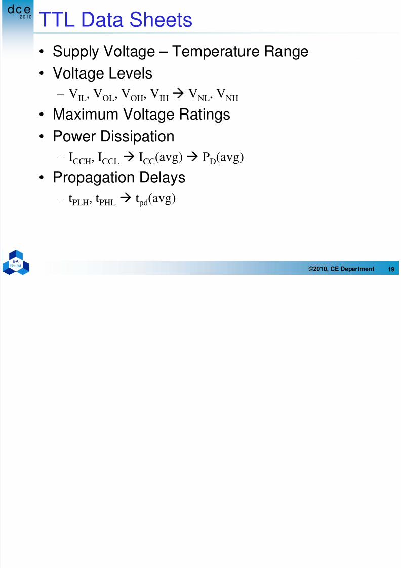
TTL Data Sheets
• Supply Voltage – Temperature Range• Voltage Levels
– VIL, VOL, VOH, VIHÆ
VNL, VNH
• Maximum Voltage Ratings
• Power Dissipation
– ICCH, ICCLÆ ICC(avg)Æ PD(avg)
• Propagation Delays
– tPLH, tPHLÆ tpd(avg)
dc e
TTL D Sh
7/30/2019 Chapter1_Integrated-Circuit Logic Family
http://slidepdf.com/reader/full/chapter1integrated-circuit-logic-family 20/52
2010
dc e
20 ©2010, CE Department
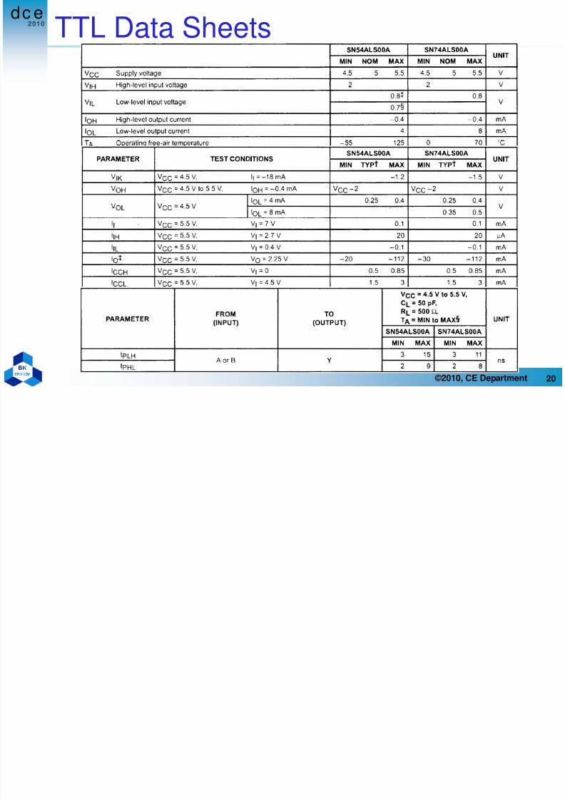
TTL Data Sheets
dc e
TTL D t Sh t
7/30/2019 Chapter1_Integrated-Circuit Logic Family
http://slidepdf.com/reader/full/chapter1integrated-circuit-logic-family 21/52
2010
dc e
21 ©2010, CE Department
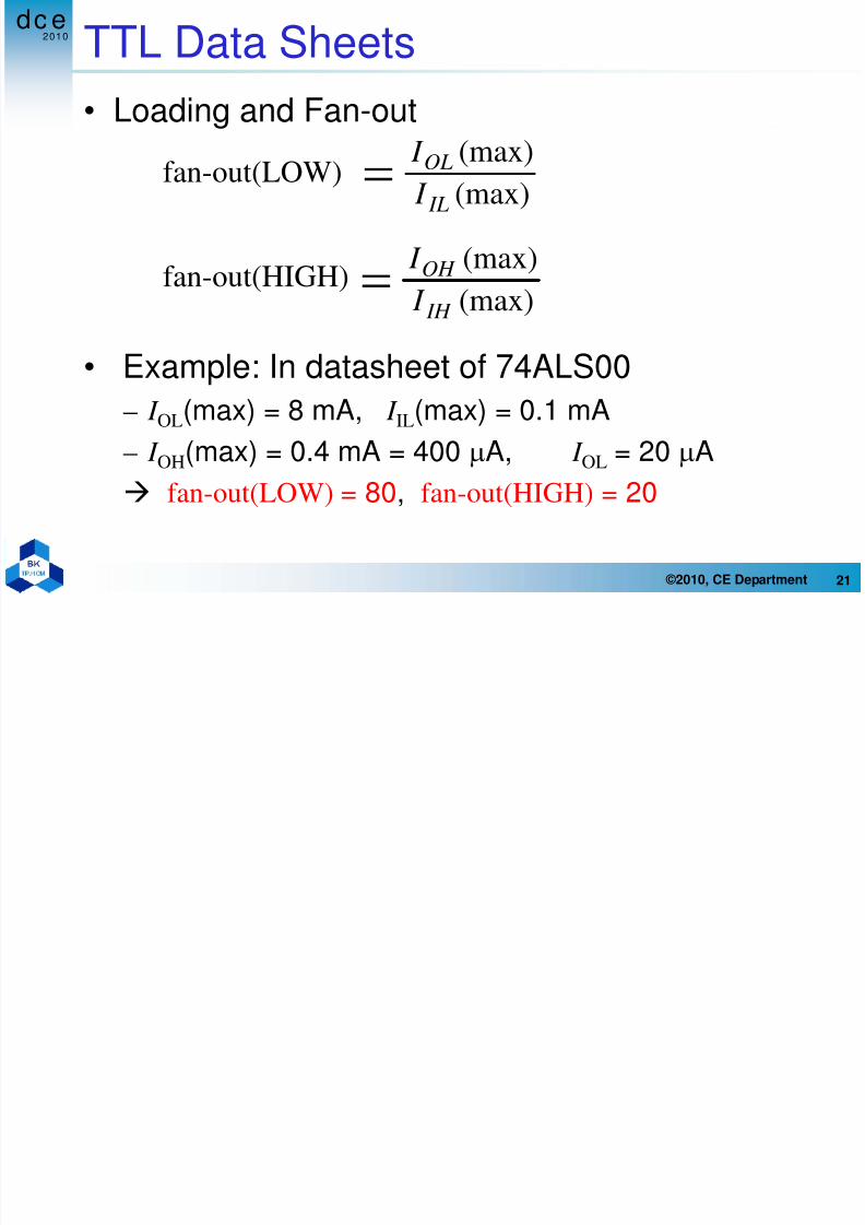
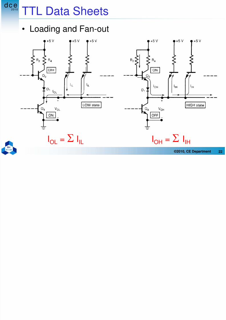
TTL Data Sheets
• Loading and Fan-out
fan-out(LOW)
fan-out(HIGH)
• Example: In datasheet of 74ALS00
– I OL(max) = 8 mA, I IL(max) = 0.1 mA– I OH(max) = 0.4 mA = 400 μA, I OL = 20 μA
Æ fan-out(LOW) = 80, fan-out(HIGH) = 20
(max)
(max)
IL
OL
I
I =
(max)
(max)
IH
OH
I
I =
dc e
TTL D t Sh t
7/30/2019 Chapter1_Integrated-Circuit Logic Family
http://slidepdf.com/reader/full/chapter1integrated-circuit-logic-family 22/52
2010
22 ©2010, CE Department
TTL Data Sheets
• Loading and Fan-out
IOL = Σ IIL IOH = Σ IIH
dc e
Oth TTL Ch t i ti
7/30/2019 Chapter1_Integrated-Circuit Logic Family
http://slidepdf.com/reader/full/chapter1integrated-circuit-logic-family 23/52
2010
23 ©2010, CE Department
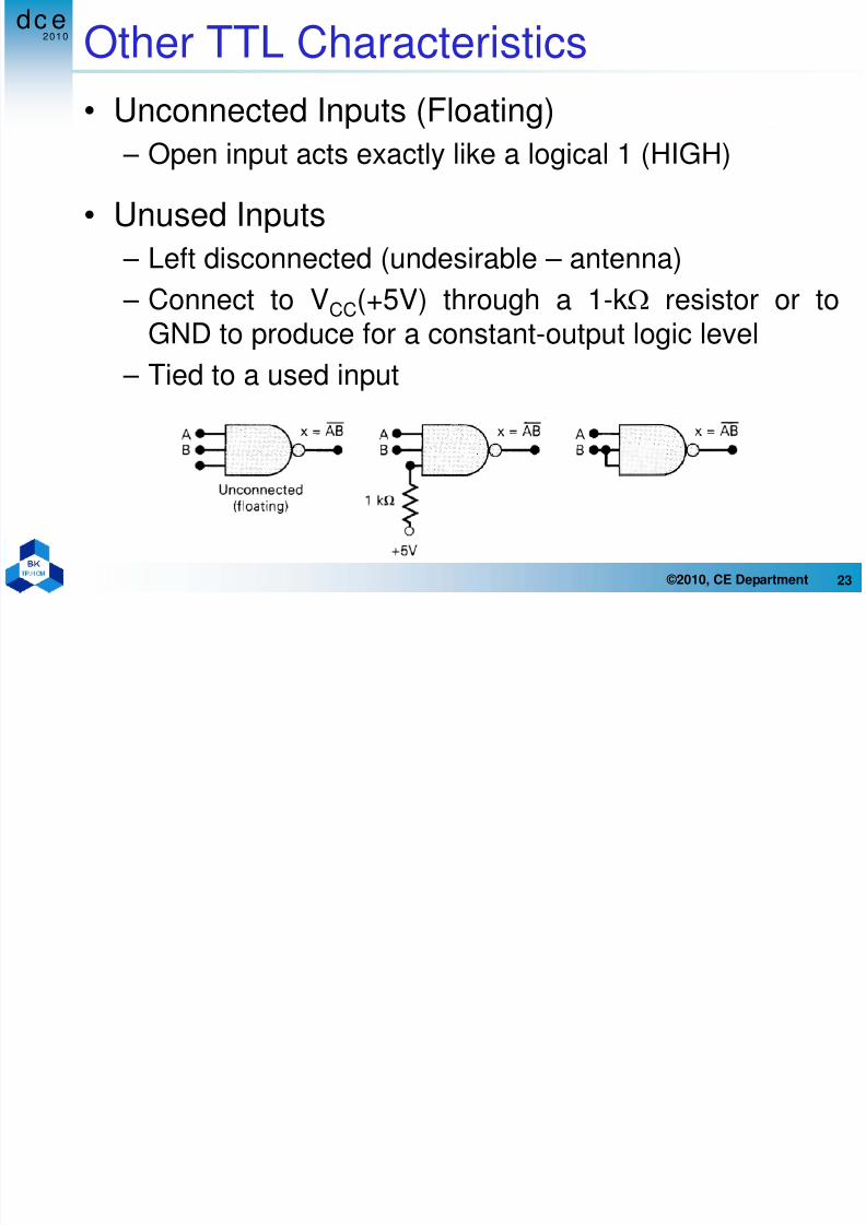
Other TTL Characteristics
• Unconnected Inputs (Floating) – Open input acts exactly like a logical 1 (HIGH)
• Unused Inputs – Left disconnected (undesirable – antenna)
– Connect to VCC
(+5V) through a 1-kΩ resistor or toGND to produce for a constant-output logic level
– Tied to a used input
2010
dc e
Oth TTL Ch t i ti
7/30/2019 Chapter1_Integrated-Circuit Logic Family
http://slidepdf.com/reader/full/chapter1integrated-circuit-logic-family 24/52
2010
24 ©2010, CE Department
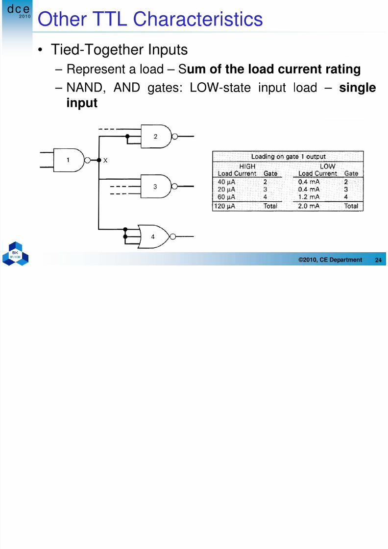
Other TTL Characteristics
• Tied-Together Inputs – Represent a load – Sum of the load current rating
– NAND, AND gates: LOW-state input load – singleinput
2010
dc e
Other TTL Characteristics
7/30/2019 Chapter1_Integrated-Circuit Logic Family
http://slidepdf.com/reader/full/chapter1integrated-circuit-logic-family 25/52
2010
25 ©2010, CE Department
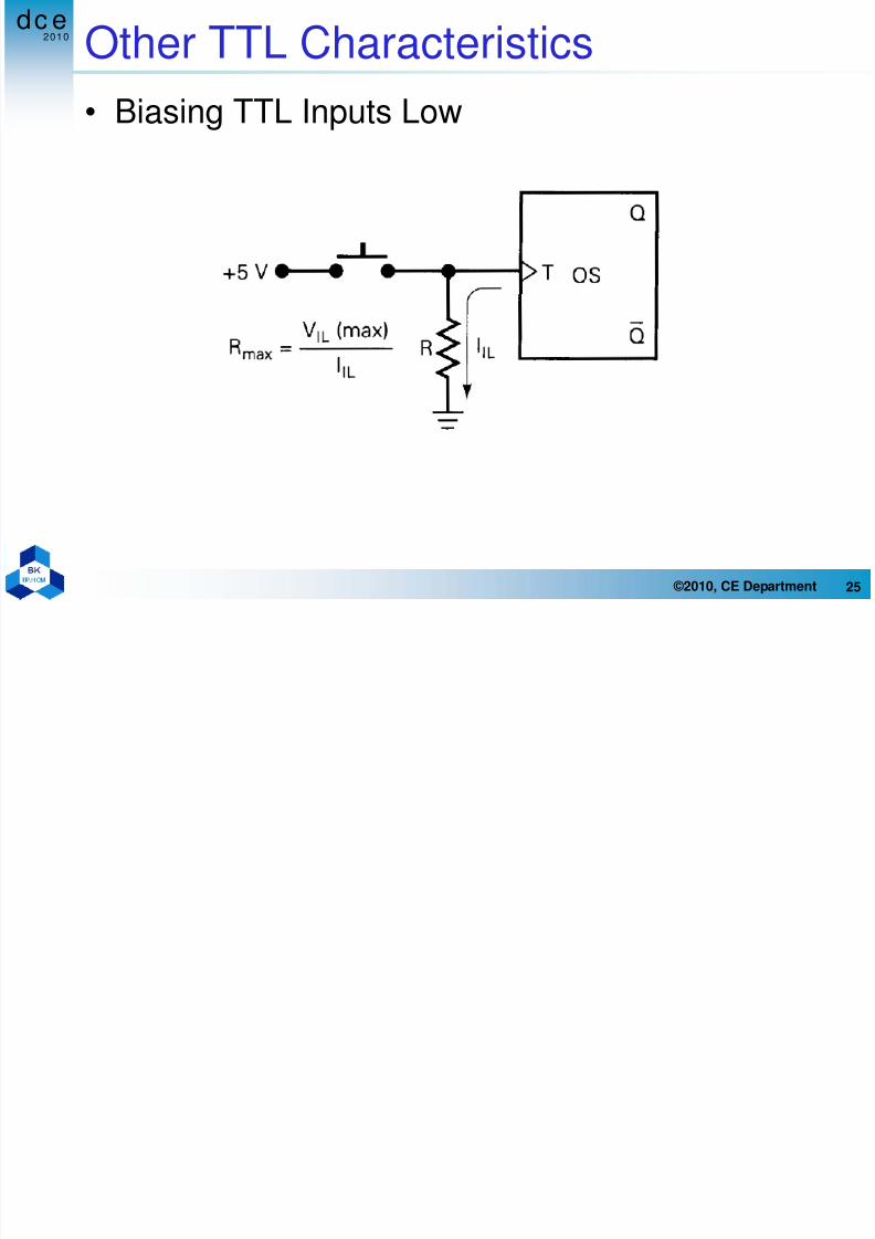
Other TTL Characteristics
• Biasing TTL Inputs Low
2010
dc e
Other TTL Characteristics
7/30/2019 Chapter1_Integrated-Circuit Logic Family
http://slidepdf.com/reader/full/chapter1integrated-circuit-logic-family 26/52
2010
26 ©2010, CE Department
Other TTL Characteristics
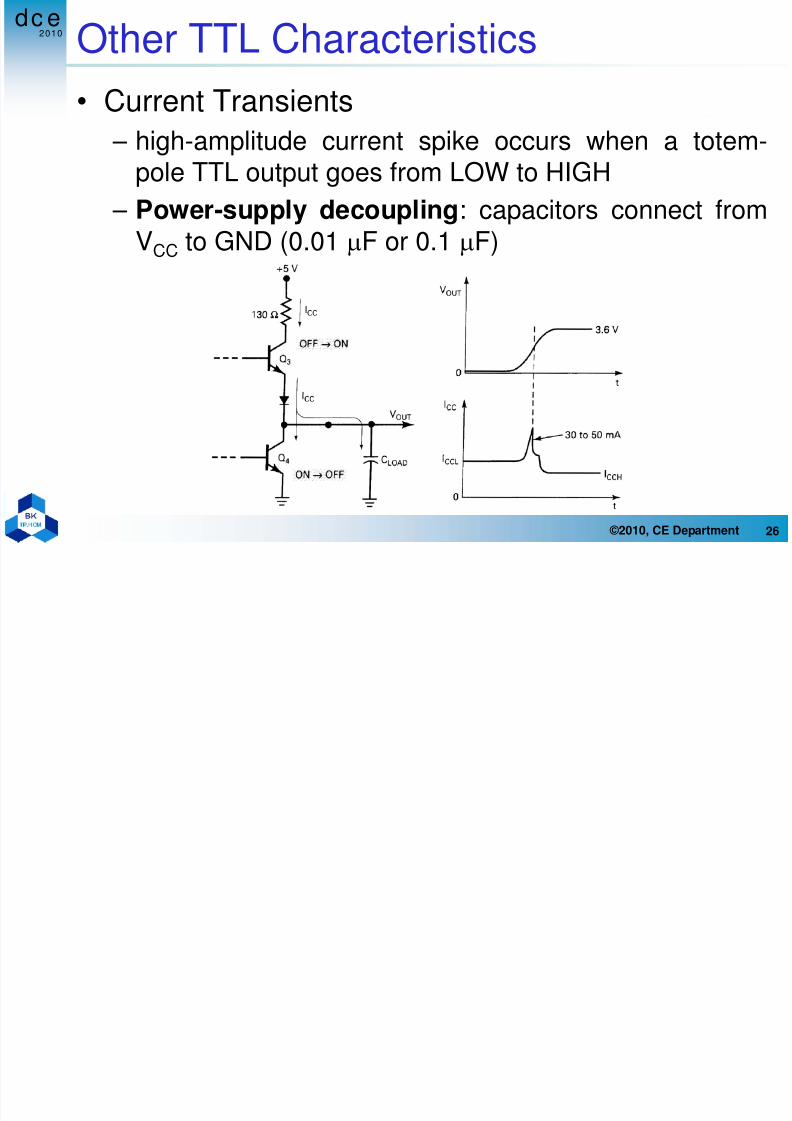
• Current Transients – high-amplitude current spike occurs when a totem-
pole TTL output goes from LOW to HIGH
– Power-supply decoupling: capacitors connect from
VCC to GND (0.01 μF or 0.1 μF)
2010
dc e
MOSFET
7/30/2019 Chapter1_Integrated-Circuit Logic Family
http://slidepdf.com/reader/full/chapter1integrated-circuit-logic-family 27/52
2010
27 ©2010, CE Department
MOSFET
• Metal-oxide-semiconductor field-effect transistor.• Advantage
– Simple, inexpensive to fabricate – Small, little power consumption
– Suited for complex ICs
– Faster than 74, 74LS, 74ALS TTL Series
• Disadvantage
– susceptibility to static-electricity damage
2010
dc e
Enhancement MOSFET
7/30/2019 Chapter1_Integrated-Circuit Logic Family
http://slidepdf.com/reader/full/chapter1integrated-circuit-logic-family 28/52
2010
28 ©2010, CE Department
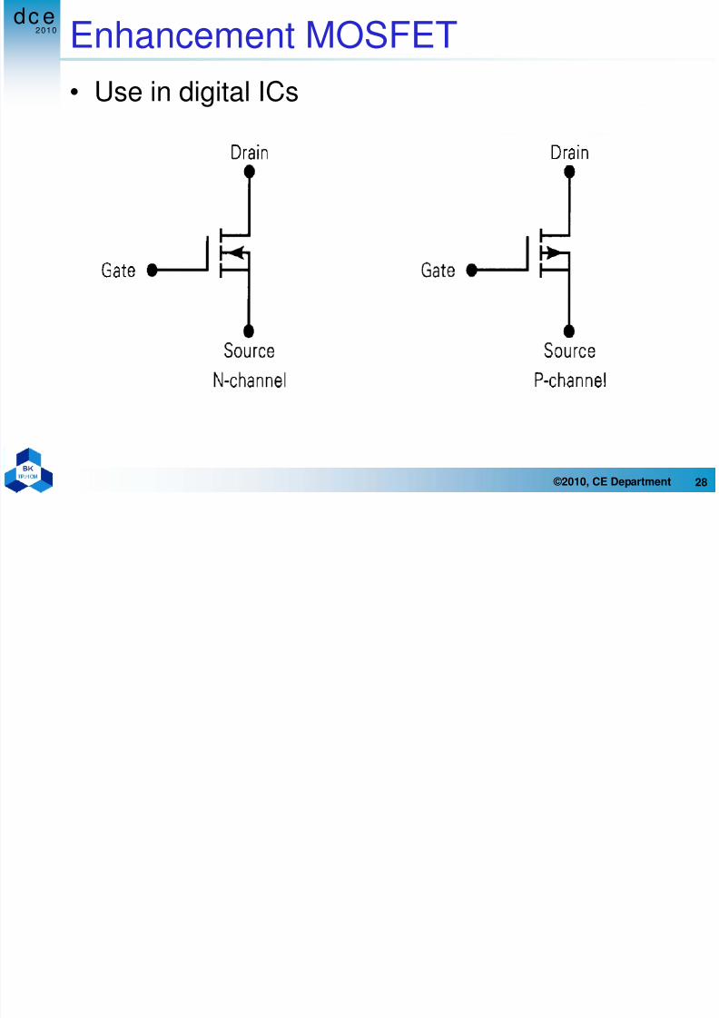
Enhancement MOSFET
• Use in digital ICs
2010
dc e
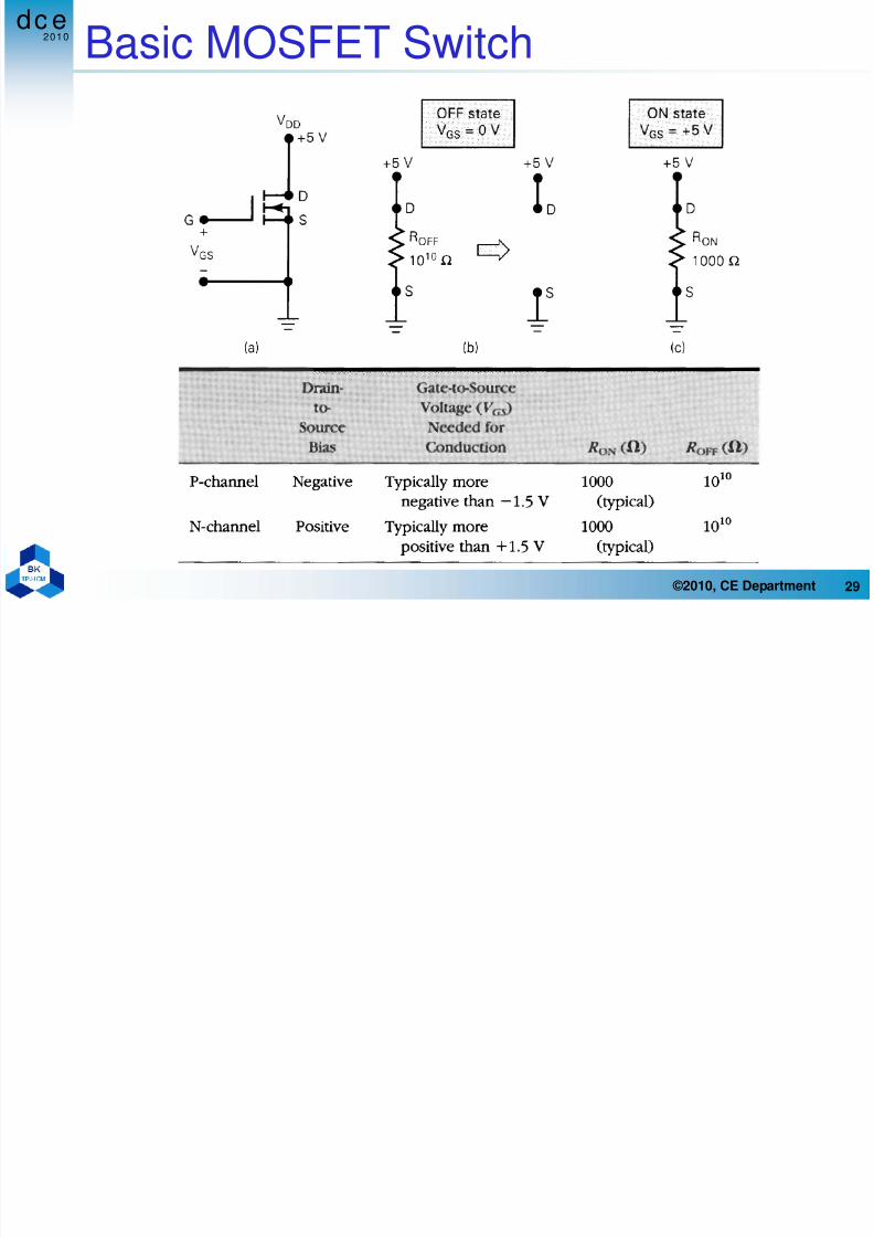
Basic MOSFET Switch
7/30/2019 Chapter1_Integrated-Circuit Logic Family
http://slidepdf.com/reader/full/chapter1integrated-circuit-logic-family 29/52
29 ©2010, CE Department
Basic MOSFET Switch
2010
dc e
Digital MOSFET Circuit
7/30/2019 Chapter1_Integrated-Circuit Logic Family
http://slidepdf.com/reader/full/chapter1integrated-circuit-logic-family 30/52
30 ©2010, CE Department
Digital MOSFET Circuit
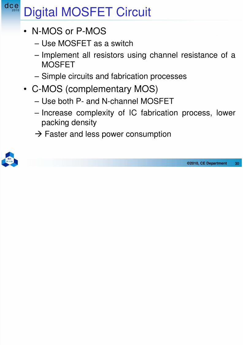
• N-MOS or P-MOS – Use MOSFET as a switch
– Implement all resistors using channel resistance of aMOSFET
– Simple circuits and fabrication processes
• C-MOS (complementary MOS) – Use both P- and N-channel MOSFET
– Increase complexity of IC fabrication process, lower
packing density
Æ Faster and less power consumption
2010
dc e
N MOS Inverter
7/30/2019 Chapter1_Integrated-Circuit Logic Family
http://slidepdf.com/reader/full/chapter1integrated-circuit-logic-family 31/52
31 ©2010, CE Department
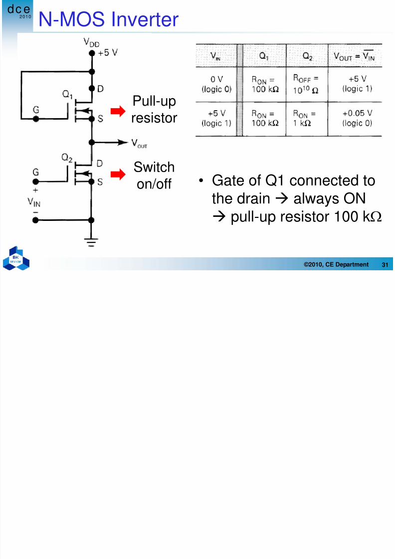
N-MOS Inverter
• Gate of Q1 connected to
the drainÆ always ONÆ pull-up resistor 100 kΩ
Pull-upresistor
Switchon/off
2010
dc e
Complementary MOS Logic
7/30/2019 Chapter1_Integrated-Circuit Logic Family
http://slidepdf.com/reader/full/chapter1integrated-circuit-logic-family 32/52
32 ©2010, CE Department
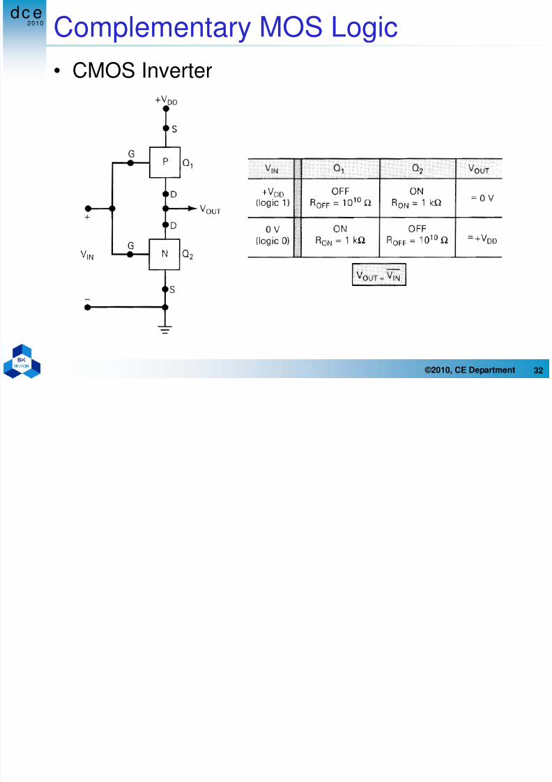
Complementary MOS Logic
• CMOS Inverter
2010
dc e
Complementary MOS Logic
7/30/2019 Chapter1_Integrated-Circuit Logic Family
http://slidepdf.com/reader/full/chapter1integrated-circuit-logic-family 33/52
33 ©2010, CE Department
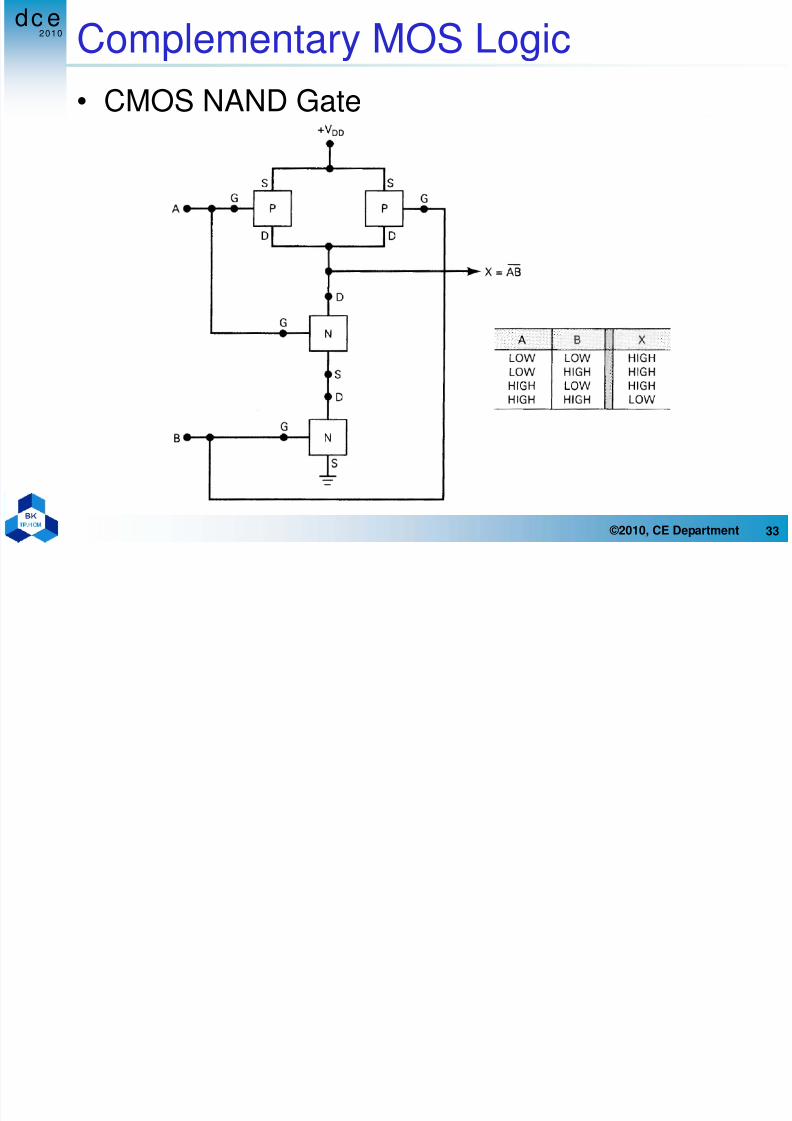
Complementary MOS Logic
• CMOS NAND Gate
2010
dc e
Complementary MOS Logic
7/30/2019 Chapter1_Integrated-Circuit Logic Family
http://slidepdf.com/reader/full/chapter1integrated-circuit-logic-family 34/52
34 ©2010, CE Department
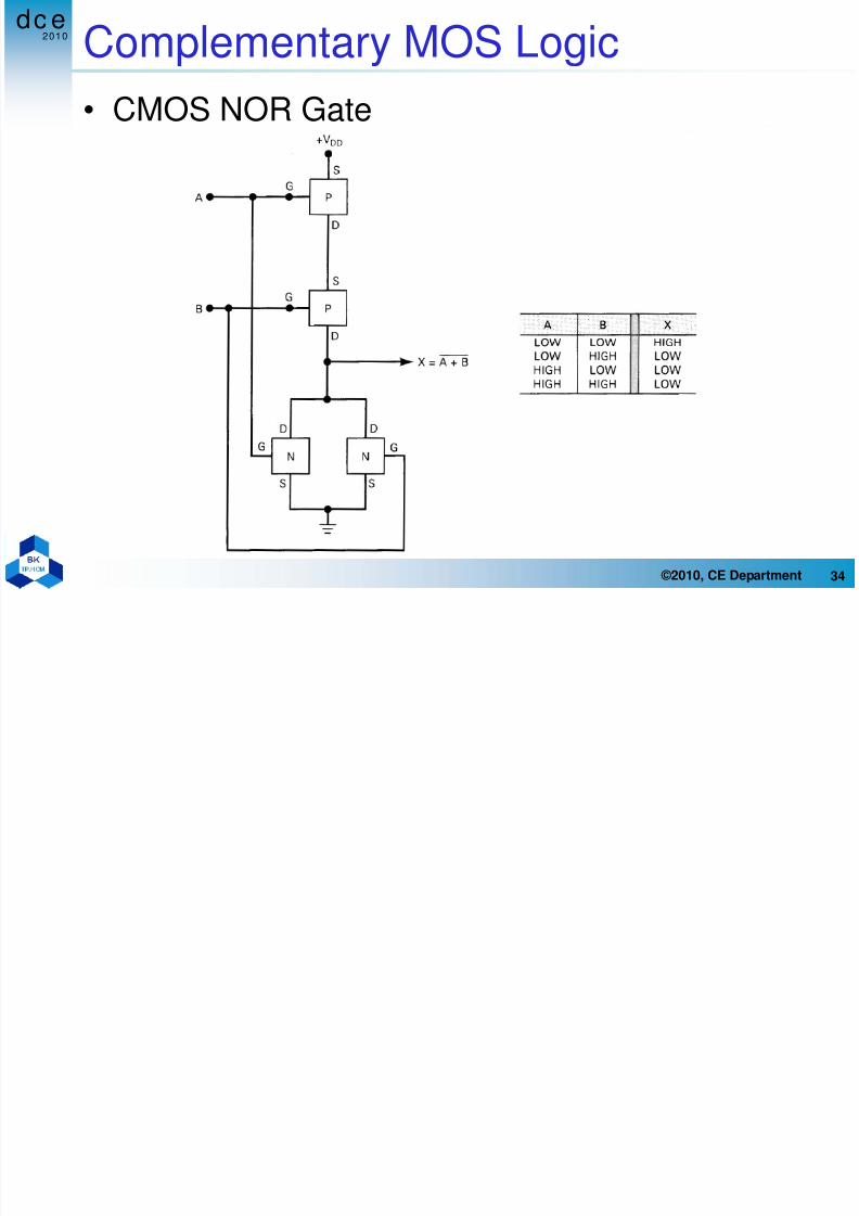
Complementary MOS Logic
• CMOS NOR Gate
2010
dc e
CMOS Series
7/30/2019 Chapter1_Integrated-Circuit Logic Family
http://slidepdf.com/reader/full/chapter1integrated-circuit-logic-family 35/52
35 ©2010, CE Department
CMOS Series
• 4000/14000 Series• 74C Series
• 74HC/HCT (High-Speed CMOS )• 74AC/ACT ( Advanced CMOS )
• 74AHC/74AHCT ( Advanced High-Speed CMOS )
• BICMOS 5-Volt Logic
2010
dc e
Low-Voltage Technology
7/30/2019 Chapter1_Integrated-Circuit Logic Family
http://slidepdf.com/reader/full/chapter1integrated-circuit-logic-family 36/52
36 ©2010, CE Department
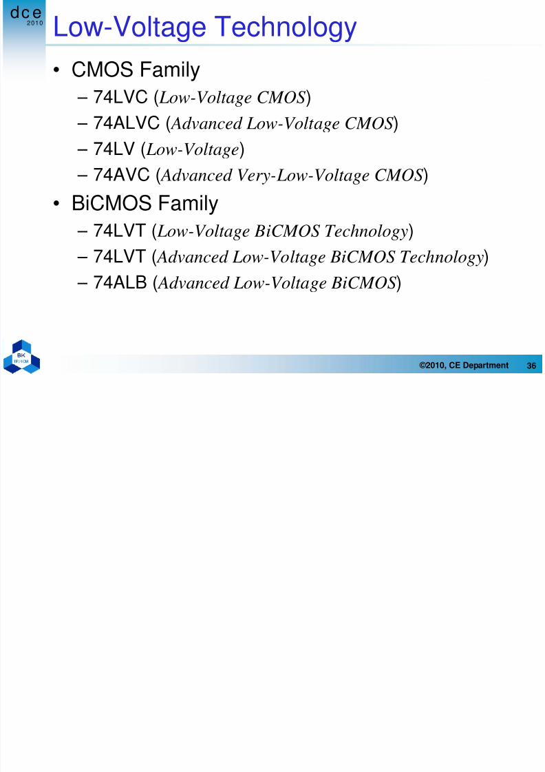
Low Voltage Technology
• CMOS Family – 74LVC ( Low-Voltage CMOS )
– 74ALVC ( Advanced Low-Voltage CMOS )
– 74LV ( Low-Voltage)
– 74AVC ( Advanced Very-Low-Voltage CMOS )
• BiCMOS Family – 74LVT ( Low-Voltage BiCMOS Technology)
– 74LVT ( Advanced Low-Voltage BiCMOS Technology)
– 74ALB ( Advanced Low-Voltage BiCMOS )
2010
dc e
CMOS Characteristics (1)
7/30/2019 Chapter1_Integrated-Circuit Logic Family
http://slidepdf.com/reader/full/chapter1integrated-circuit-logic-family 37/52
37 ©2010, CE Department
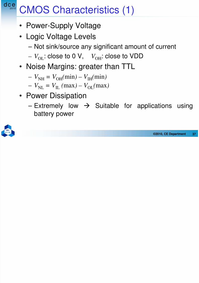
CMOS Characteristics (1)
• Power-Supply Voltage• Logic Voltage Levels
– Not sink/source any significant amount of current
– V OL: close to 0 V, V OH: close to VDD
• Noise Margins: greater than TTL
– V NH = V OH(min) – V IH(min)
– V NL = V IL (max) – V OL(max)
• Power Dissipation – Extremely low Æ Suitable for applications using
battery power
2010
dc e
CMOS Characteristics (2)
7/30/2019 Chapter1_Integrated-Circuit Logic Family
http://slidepdf.com/reader/full/chapter1integrated-circuit-logic-family 38/52
38 ©2010, CE Department
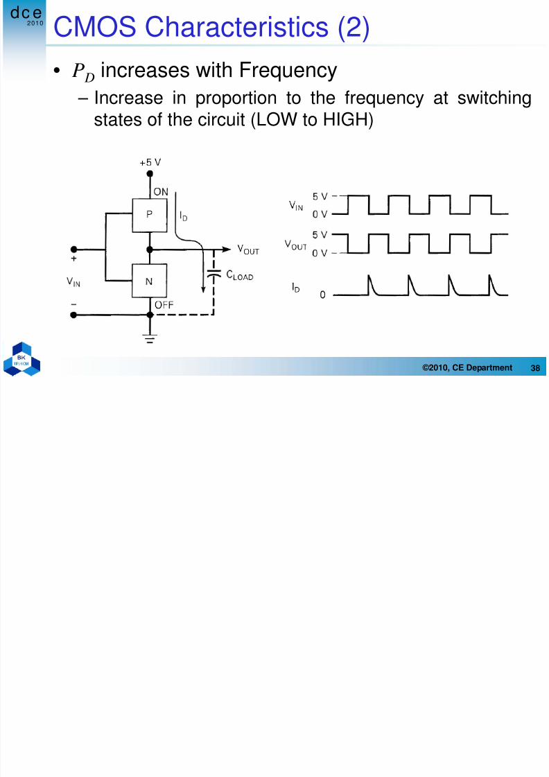
CMOS Characteristics (2)
• P D increases with Frequency – Increase in proportion to the frequency at switching
states of the circuit (LOW to HIGH)
2010
dc e
CMOS Characteristics (3)
7/30/2019 Chapter1_Integrated-Circuit Logic Family
http://slidepdf.com/reader/full/chapter1integrated-circuit-logic-family 39/52
39 ©2010, CE Department
CMOS Characteristics (3)
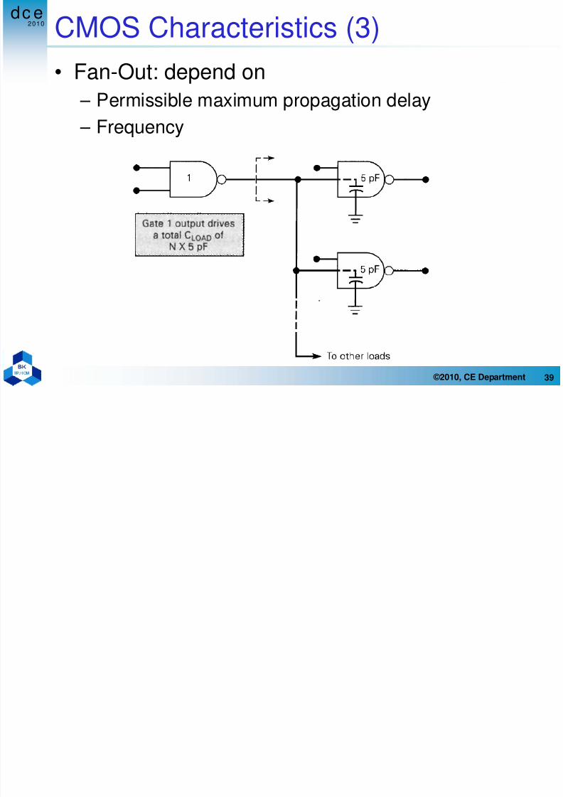
• Fan-Out: depend on – Permissible maximum propagation delay
– Frequency
2010
dc e
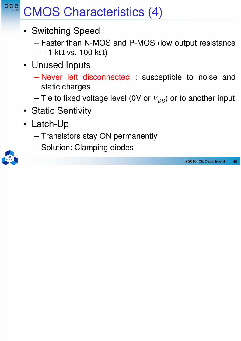
CMOS Characteristics (4)
7/30/2019 Chapter1_Integrated-Circuit Logic Family
http://slidepdf.com/reader/full/chapter1integrated-circuit-logic-family 40/52
40 ©2010, CE Department
CMOS Characteristics (4)
• Switching Speed – Faster than N-MOS and P-MOS (low output resistance
– 1 kΩ vs. 100 kΩ)
• Unused Inputs
– Never left disconnected : susceptible to noise and
static charges – Tie to fixed voltage level (0V or V DD) or to another input
• Static Sentivity
• Latch-Up
– Transistors stay ON permanently
– Solution: Clamping diodes
2010
dc e
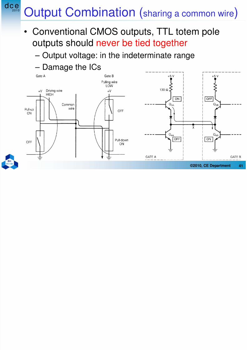
Output Combination (sharing a common wire)
7/30/2019 Chapter1_Integrated-Circuit Logic Family
http://slidepdf.com/reader/full/chapter1integrated-circuit-logic-family 41/52
41 ©2010, CE Department
Output Co b at o ( g )
• Conventional CMOS outputs, TTL totem poleoutputs should never be tied together
– Output voltage: in the indeterminate range
– Damage the ICs
2010
dc e
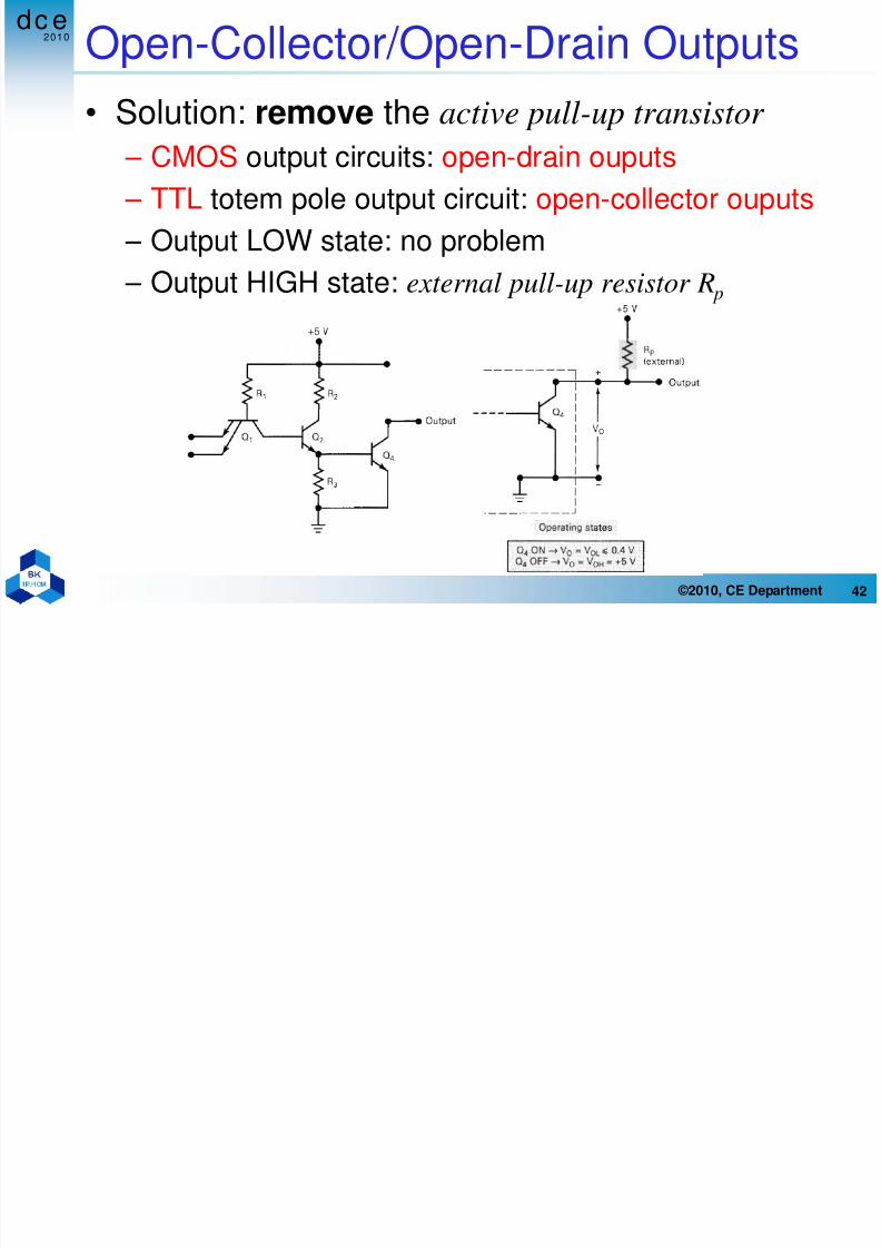
Open-Collector/Open-Drain Outputs
7/30/2019 Chapter1_Integrated-Circuit Logic Family
http://slidepdf.com/reader/full/chapter1integrated-circuit-logic-family 42/52
42 ©2010, CE Department
p p p
• Solution: remove the active pull-up transistor – CMOS output circuits: open-drain ouputs
– TTL totem pole output circuit: open-collector ouputs
– Output LOW state: no problem
– Output HIGH state: external pull-up resistor R p
2010
dc e
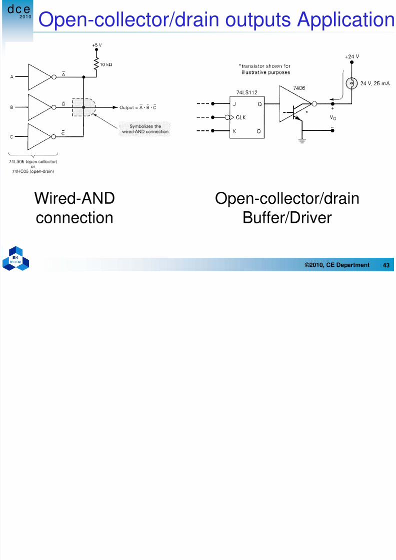
Open-collector/drain outputs Application
7/30/2019 Chapter1_Integrated-Circuit Logic Family
http://slidepdf.com/reader/full/chapter1integrated-circuit-logic-family 43/52
43 ©2010, CE Department
p p pp
Wired-ANDconnection
Open-collector/drainBuffer/Driver
2010
dc e
Tristate (Three-State) Logic Ouputs
7/30/2019 Chapter1_Integrated-Circuit Logic Family
http://slidepdf.com/reader/full/chapter1integrated-circuit-logic-family 44/52
44 ©2010, CE Department
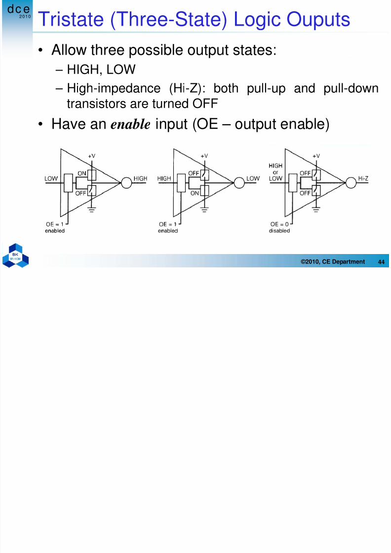
( ) g p
• Allow three possible output states: – HIGH, LOW
– High-impedance (Hi-Z): both pull-up and pull-down
transistors are turned OFF
• Have an enable input (OE – output enable)
2010
dc e
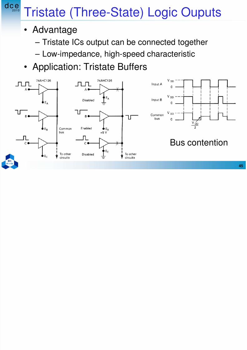
Tristate (Three-State) Logic Ouputs
7/30/2019 Chapter1_Integrated-Circuit Logic Family
http://slidepdf.com/reader/full/chapter1integrated-circuit-logic-family 45/52
45
( ) g p
• Advantage – Tristate ICs output can be connected together
– Low-impedance, high-speed characteristic
• Application: Tristate Buffers
Bus contention
2010dc e
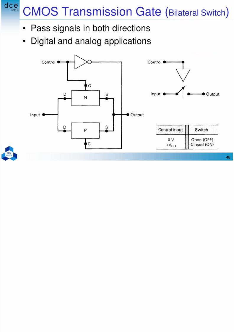
CMOS Transmission Gate (Bilateral Switch)
7/30/2019 Chapter1_Integrated-Circuit Logic Family
http://slidepdf.com/reader/full/chapter1integrated-circuit-logic-family 46/52
46
( )
• Pass signals in both directions• Digital and analog applications
2010dc e
IC Interfacing
7/30/2019 Chapter1_Integrated-Circuit Logic Family
http://slidepdf.com/reader/full/chapter1integrated-circuit-logic-family 47/52
47
• Connecting the output(s) to the input(s) ofdifferent electrical charateristic systems.
• Take advange of the strong points of each IC
family – High-speed, greater output current/voltage capability,
high frequency
• Concerned problems
– Fan-out
– Voltage and current parameters
2010dc e
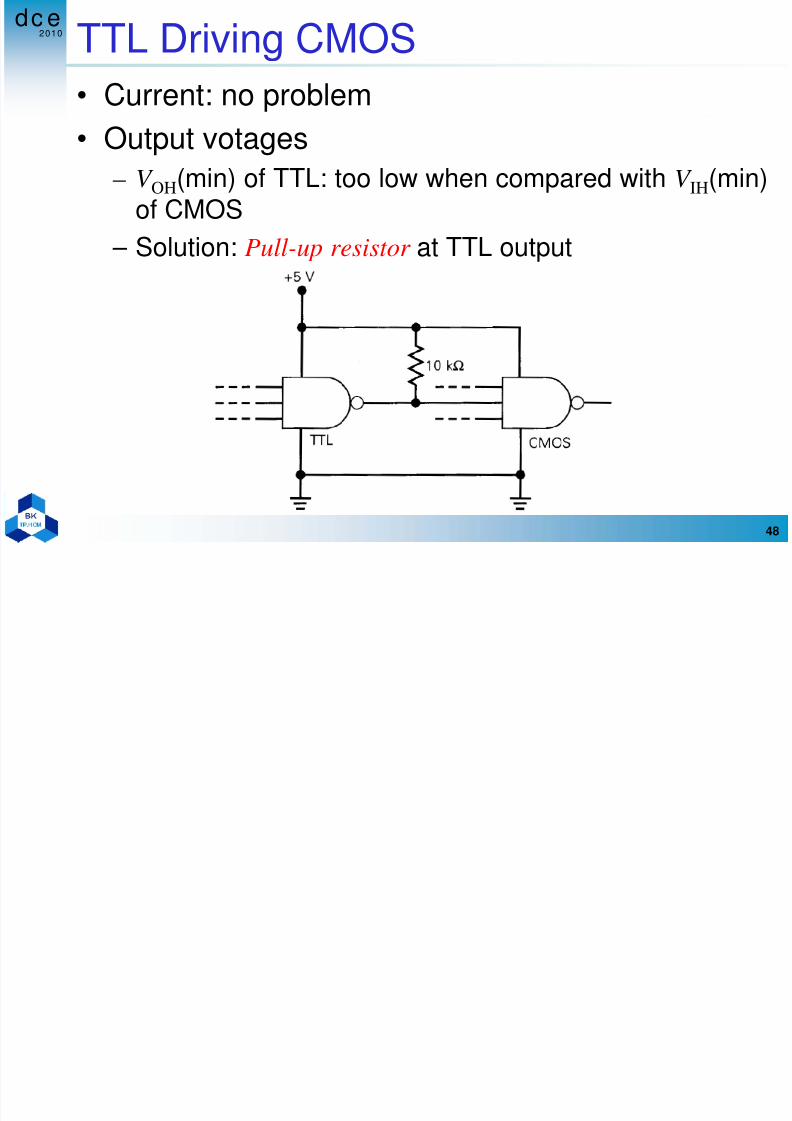
TTL Driving CMOS
7/30/2019 Chapter1_Integrated-Circuit Logic Family
http://slidepdf.com/reader/full/chapter1integrated-circuit-logic-family 48/52
48
• Current: no problem• Output votages
– V OH(min) of TTL: too low when compared with V IH(min)
of CMOS
– Solution: Pull-up resistor at TTL output
2010dc e
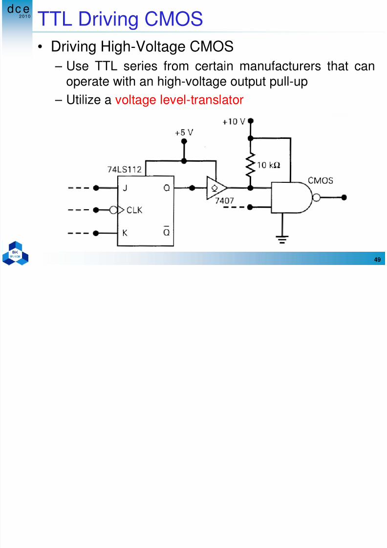
TTL Driving CMOS
7/30/2019 Chapter1_Integrated-Circuit Logic Family
http://slidepdf.com/reader/full/chapter1integrated-circuit-logic-family 49/52
49
• Driving High-Voltage CMOS – Use TTL series from certain manufacturers that can
operate with an high-voltage output pull-up
– Utilize a voltage level-translator
2010dc e
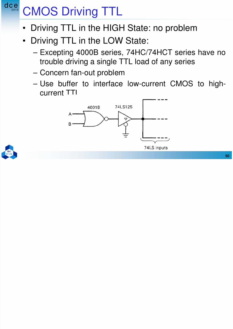
CMOS Driving TTL
7/30/2019 Chapter1_Integrated-Circuit Logic Family
http://slidepdf.com/reader/full/chapter1integrated-circuit-logic-family 50/52
50
• Driving TTL in the HIGH State: no problem• Driving TTL in the LOW State:
– Excepting 4000B series, 74HC/74HCT series have no
trouble driving a single TTL load of any series
– Concern fan-out problem
– Use buffer to interface low-current CMOS to high-current TTL
2010dc e
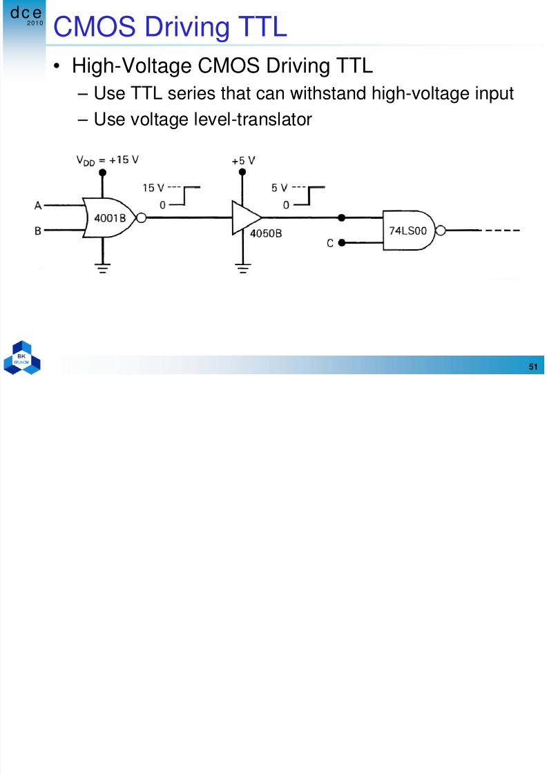
CMOS Driving TTL
7/30/2019 Chapter1_Integrated-Circuit Logic Family
http://slidepdf.com/reader/full/chapter1integrated-circuit-logic-family 51/52
51
• High-Voltage CMOS Driving TTL – Use TTL series that can withstand high-voltage input
– Use voltage level-translator
2010dc e
Reference
7/30/2019 Chapter1_Integrated-Circuit Logic Family
http://slidepdf.com/reader/full/chapter1integrated-circuit-logic-family 52/52
52
• Chapter 8, Digital System – Principles andApplications, Ronald J.Tocci, Neal S. Widmer