Embed Size (px)
Citation preview

Chapter 9Digital Signal Processing
with Xilinx FPGAs
Yin-Tsung Hwang
The materials are largely based on the Xilinx Seminar Notes presented by Bruce Newgard
2
Configurable Hardware DSP Solutions Introduction to digital filters Distributed Arithmetic (DA) DA FIR filter example 8 Tap Slice High speed FIR filter Low speed FIR filter IIR bi-quad filter correlator Summary

Digital Filter Basics
4
Introduction to Digital Filters Key component in many DSP applications
channel equalization, echo cancellation
digital vs analog filters programmability better frequency response
Classifications Finite Impulse Response (FIR) filter
Infinite Impulse Response (IIR) filter
1
0
)()(M
kk knxcny
1
0 1
)()()(M
k
N
ppk pnybknxcny

5
Finite Impulse Response Filter
ck: filter coefficients (constants) x(n): input at time instance n y(n): output at time instance n M: filter tap order
M could be as large as 1000
a series of multiply and accumulate operations No. of MAC operations /sec = sampling frequency
filter tap order
)1()1()(
)()(
110
1
0
Mnxcnxcnxc
knxcny
M
M
kk
6
High Pass Filter Example
0 10 20 30 40 50 60 70-0.2
-0.15
-0.1
-0.05
0
0.05
0.1
0.15
0.2
0.25
n
|h(n
)|
coefficients
-2 -1.5 -1 -0.5 0 0.5 1
-1
-0.5
0
0.5
1
Real part
Ima
gin
ary
pa
rt
0 1000 2000 3000 4000 5000 6000 7000 8000 9000-60
-50
-40
-30
-20
-10
0
frequency
de
cib
els
Magnitude Response in dB
Ws=1500Hz Wp=4000HzSampling freq. : 5KHzTap order : 67filter type :HPF filter(FIR)

7
Low Pass Filter Example
Wp=1500Hz Ws=3000HzSample_freq=5KHzTap order=67filter type : LPF filter(FIR)
0 10 20 30 40 50 60 70-0.02
0
0.02
0.04
0.06
0.08
0.1
n
|h(n
)|coefficient
-2 -1.5 -1 -0.5 0 0.5 1
-1
-0.5
0
0.5
1
Real part
Ima
gin
ary
pa
rt
0 0 .5 1 1 .5 2 2 .5
x 104
-140
-120
-100
-80
-60
-40
-20
0
20
frequency
de
cib
els
Magn itude Response in dB
8
Basic FIR Filter Block Diagram

9
FIR Implementation Using Programmable DSP Processor
Software solution
1 parallel multiplier, accumulator
Time sharing through micro-coding
relative low sample rate
multiple chip solution
no migration path
complex real time programmingFor each sample data word
For each tapMultiply c(i) times x(i)Add result to accumulator
Distributed Arithmetic Basics

11
2’s Complement Multiplication
12
A Series of Multiply & Add
×
+
+
×
+
+
×
+
coefficient Input sampleWeighted
partial product
multiply result
+final result
Parallel multiplier
accumulator

13
Distributed Arithmetic Approach (1)
+ + + +
LSB MSBLSB+1
+final result
partial sumCan be implementedby a look up table
Accumulator + shifter
14
Distributed Arithmetic Approach (2) x x x x3,3 0,0 3,2 0,0 3,1 0,0 3,0 0,0a a a a
Sum Sum Sum Sum SumSum
x x x x2,3 1,0 2,2 1,0 2,1 1,0 2,0 1,0a a a a x x x x1,3 2,0 2,2 2,0 1,1 2,0 1,0 2,0a a a a x x x x0,3 3,0 0,2 3,0 3,1 0,0 3,0 0,0a a a a
x x x x3,3 0,1 3,2 0,1 3,1 0,1 3,0 0,1a a a a x x x x2,3 1,1 2,2 1,1 2,1 1,1 2,0 1,1a a a a x x x x1,3 2,1 1,2 2,1 1,1 2,1 1,0 2,1a a a a x x x x0,3 3,1 0,2 3,1 0,1 3,1 0,0 3,1a a a a
Sum Sum Sum Sum SumSum x x x x3,3 0,2 3,2 0,2 3,1 0,2 3,0 0,2a a a a x x x x2,3 1,2 2,2 1,2 2,1 1,2 2,0 1,2a a a a x x x x1,3 2,2 1,2 2,2 1,1 2,2 1,0 2,2a a a a x x x x0,3 3,2 0,2 3,2 0,1 3,2 0,0 3,2a a a a
x x x x3,3 0,3 3,2 0,3 3,1 0,3 3,0 0,3a a a a
Sum Sum Sum Sum SumSum
x x x x2,3 1,3 2,2 1,3 2,1 1,3 2,0 1,3a a a a x x x x1,3 2,3 1,2 2,3 1,1 2,3 1,0 2,3a a a a x x x x0,3 3,3 0,2 3,3 0,1 3,3 0,0 3,3a a a a
Sum Sum Sum Sum SumSum
SumSum Sum Sum SumSumSumSum Sum Sum SumSum
SumSum Sum Sum SumSumSumSum Sum Sum SumSum
+1
+1
+1
+1
1
1
1
1
P 0P 1P 2P 3P 4P 5P 6P 7P 8P 9
Need a 4-operandparallel adder
Need a scalingaccumulator

15
DA One-Tap FIR Filter Reduces to multiply a variable x(n) with a constant c0
16
DA Two-Tap FIR Filter

17
DA Three-Tap FIR Filter
Look up table implementation can be both faster and area efficient than a multi-operand adder
18
Recall XC4000X Family
4028EX* 4036EX* 4044EX 4052XL 4062XL 4085XL 40125XV4028EX* 4036EX* 4044EX 4052XL 4062XL 4085XL 40125XV
Typ Logic Gates
Typ System Gates(Logic + Select -
RAM)
Avail RAM bits
Number CLBs
Flip-Flops
I/O
Supply Voltage
Packages:
Typ Logic Gates
Typ System Gates(Logic + Select -
RAM)
Avail RAM bits
Number CLBs
Flip-Flops
I/O
Supply Voltage
Packages:
56,000 72,000 90,000 110,000 130,000 175,000 250,000
32,768 41,472 51,200 61,952 73,728 100,352 157,968
1,024 1,296 1,600 1,936 2,304 3,136 4,6242,560 3,168 3,840 4,576 5,376 7,168 10,336256 288 320 352 384 448 544
HQ208 HQ208 HQ208HQ240 HQ240 HQ240 HQ240 HQ240HQ304 HQ304 HQ304 HQ304 HQ304 BG352 BG352 BG352 BG352 BG352
BG432 BG432 BG432 BG432BG560 BG560 BG560 BG560
PG299 PG411 PG411 PG411 PG475 PG559 PG599
* 30% of CLBsas RAM
28,000 36,000 44,000 52,000 62,000 85,000 125,000
5/3 5/3 5/3 3 3 3 2.5

The Development of a Distributed Arithmetic FIR Filter
10 bit 10 tap XC4000E Family example
20
DA FIR Filter Design in XC 4000E
10-Tap 10-bit example
• N clocks per sample word• Fast clock• No multiplier required• Embedded hardware solution• LUT holds coefficients & Mult.

21
LUT Size in DA FIR Design• Look up table scales exponentially• 10-tap 10-bit needs 210×10 bits• need to reduce the LUT size• take advantages of linear phasesymmetrical FIR filter
22
10-Tap 10-Bit Symmetrical FIR Filter

23
Look Up Table Implementation
Holds all partial products
LUT is as wide as coefficient
use MEMGEN to generate LUT
32×10 memory
Look UpTable
A0
A1
A2
A3
A4
320 bits
DATA10
24
Serial Time Skew Buffer
Sample data word size = Nfilter tap size = k
• one N-bit shift register per tap• use XC4000E RAM to build
shift register• one 16-bit shift register per
1/2 CLB
Using FFs10-bit 10-tap50 CLBs
Using FFs10-bit 10-tap50 CLBs
Using RAMs10-bit 10-tap10 CLBs
Using RAMs10-bit 10-tap10 CLBs
Shift register implemented in RAM

25
Bit Serial Adder
Distributed arithmetic lookup table
26

27
1‘s Complementer MSB has negative
weighting inverts data on the last
cycle 2 bits per CLB
28
Scaling Accumulator
Adds data to 1/2*(SUMOUT)
2 bits per CLB
needs N+1 bits
double precision with an extra shift register
can use LogiBlox for RPM
10-bit 10-tap linear phase FIR filter
29
30
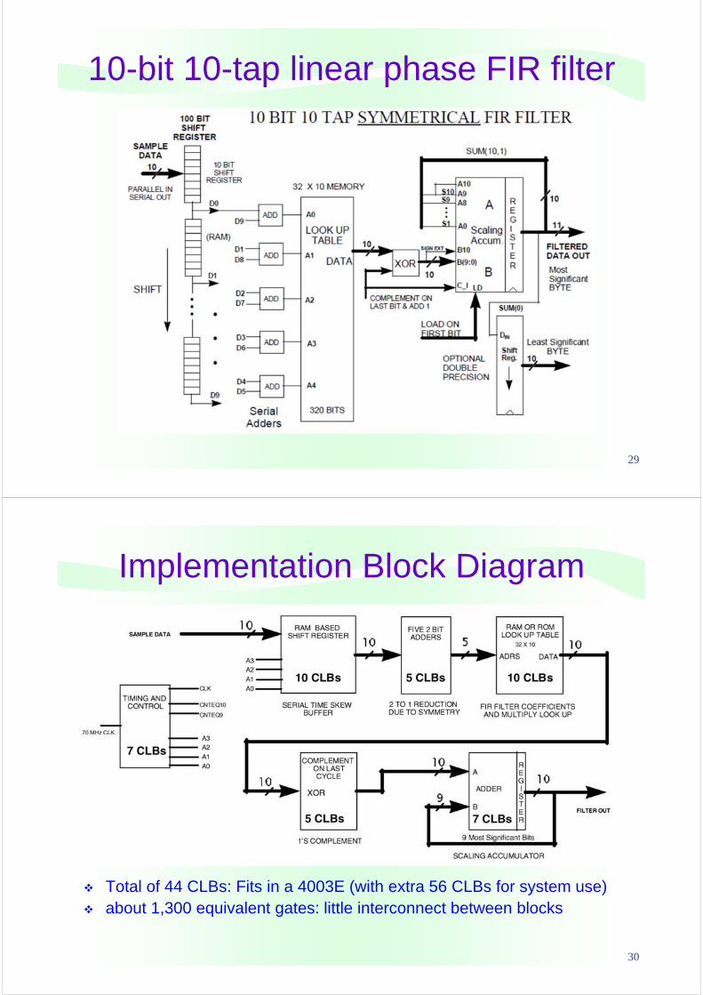
Implementation Block Diagram
Total of 44 CLBs: Fits in a 4003E (with extra 56 CLBs for system use) about 1,300 equivalent gates: little interconnect between blocks

31
Performance No. of 10-tap 10-bit sym. FIR per 4000E device
XC4000part
4003E 4005E 4006E 4008E 4010E 4013E 4020E 4025E
Number ofinstances
2 4 5 7 9 11 15 22
FIR 10B10T macro can be clocked at 70 MHz
10 bit word requires 11 clocks 10 bit sample word rate is 6.4
MHz
word sizesample rate
6 8 10 12 14 16
10.0 7.8 6.4 5.4 4.7 4.1
bitsMHz
32
Double Rate DA FIR Filter (1)
Process 2 bits per clock # of clocks = (N/2)+1

33
Double Rate DA FIR Filter (2)
two taps require 4-input LUT without symmetry
four taps require 4-input LUT with symmetrical FIR
time skew buffer is twice as many CLBs
twice the data word sample rate
both LUTs are the same
Designing large multi-tap filter Xilinx 8-tap FIR filter SLICE building blocks
34

Issue: LUT scales exponentially
35
32-tap FIR filter using 8-tap slices
36

8-tap FIR filter slice building blocks
37
8-tap FIR filter slice
38

8-tap FIR filter slice
39
Very high speed sampling rates
Multiple parallel multipliers
40

Multiply variable with a constant
41
Multiply variable with a constant (1)
42

Multiply variable with a constant (2)
43
High speed parallel FIR filter
44

Fully parallel distributed arithmetic
45
8-tap parallel DA slice (1)
46

8-tap parallel DA slice (2) Support sampling rates 50 ~ 70 Msps Data and coefficient sizes are independent of each
other 8-bit data, 8-bit coefficient require 122 CLBs per 8-
tap slice 16-tap, 8-bit filter requires 250 CLBs 32-tap, 8-bit filter requires 508 CLBs
47
CLB count for 8-tap PDA slice
Approximate number of XC4000 CLBs48

Serial sequential architecture
• Efficient CLB counts• Large number of taps• Moderate sampling rates• Non-symmetric filter OK
49
Lower sampling rate applications
Serial sequential architecture
50

Serial sequential FIR filter (1)
51
Serial sequential FIR filter (2)
52

Serial sequential FIR filter (3)
53
64-tap serial sequential FIR filter
54

Serial sequential FIR filter designs
55
Size estimate
Serial sequential FIR filter designs
56
Speed estimate

8-bit word FIR filter structures
57
FIR filter implementation options
58
8-bit word example

12-bit word FIR filter structures
59
FIR filter implementation options
60
12-bit word example

IIR Filter Designs
61
Bi-quad IIR filter – direct form
62
(lowest quantization noise)

IIR filter – bi-quad implementation
Requires 32-deep LUT 2 parallel to serial converters 60 CLBs for 16-bit word
63
64
IIR filter – bi-quad implementation

Correlator design
65
Using LUTs for correlator design Any n-stage correlator can be decomposed into
(n/4) 4-stage correlators LUTs contain all possible outputs for each 4-stage
correlation Example: correlation pattern = 1011
Store 4h at address 13h in LUT (4 bit matches) Store 3h at addresses 3, F, 9, A in LUT (1 bit error)
Bit rate can exceed 120MHz (XC 3100A)
66

Correlator LUT example
67
Input search pattern= 1101
16-stage correlator using LUT
68

Summary
70
Xilinx v.s. DSP Processor When does it make senses to use FPGAs?
High to medium sample rate systems
small word lengths
lots of taps
fast correlators
single chip solution required
low cost migration path (HardWire)
incremental cost of DSP chip
DSP application specific chips
Design Once !

71
XDSP FPGA Applications
Signal Synthesis
Modulation / Demodulation
Fast Fourier Transforms
Neural Networks
Video Signal Processing (2D, 3D Filters)
and more …….
72
Possibilities
An alternative to software DSP processor solution
existing 4000E/EX are efficient at signal processing
system level application specific solution on a single chip
standard product configurable solution
automatic migration path to a lower cost high volume solution