Embed Size (px)
Citation preview

DELIVERING HIGHEST SYSTEM PERFORMANCE WHILE REDUCING POWER CONSUMPTION
Enabling Tomorrow’s Innovations
The Xilinx Virtex®-7 Family of FPGAs breaks through previous physical limits to enable tomorrow’s innovations. A combination of ultra high-end bandwidth and capacity boosts system performance to address the most complex system requirements. The uncompromised performance is delivered as the foundation of a programmable platform, with the versatility to maximize differentiation in today’s competitive markets.
Unprecedented Throughput
With up to 96 advanced serial transceivers, the Virtex-7 FPGAs enable designers to build breakthrough bandwidth into next-generation communications solutions. The advanced throughput enables unprecedented advancements for network infrastructure, including the only single-FPGA solution for Nx100G and 400G optical networking.
New Milestones in Performance
Virtex-7 FPGAs deliver up to 2 million logic cells and more than 5TMACS DSP throughput. These resources enable massively parallel data processing architectures that perform more work with each clock cycle. With up to 88 advanced serial transceivers, Virtex-7 FPGAs offer more than 4Tbps of serial bandwidth. These capabilities enable new levels of processing performance for advanced RADAR, high-performance computing, and advanced medical imaging systems.
Exceeding Moore’s Law
Xilinx pioneered SSI technology to achieve increases in capacity and performance that exceed the pace of Moore’s Law. As a result, Virtex-7 FPGAs offer more than 3.5 times the capacity of the previous generation. Combined with the family’s memory, DSP, and I/O resources, Virtex-7 devices establish new performance benchmarks.
Low Power by Design
Industry-leading 28nm HPL process technology achieves the optimum balance of performance and power for these-next generation FPGAs. Architectural enhancements further reduce I/O power consumption while increasing bandwidth. And intelligent clock-gating algorithms in Xilinx design tool software further reduce active power consumption.
The Challenge: Insatiable Bandwidth Demand
• Implementing advanced serial connectivity standards for next-generation networks
• Increasing data processing performance
• Getting products to market faster
• Meeting restricted power budgets
The Solution: Xilinx Virtex-7 FPGAs
• 16 x 28 Gb/s transceivers to create a single-chip FPGA solution for 400G line cards
• Up to 2M logic cell capacity for building massively parallel high-performance circuits enabled by stacked-silicon interconnect (SSI) technology
• Up to 6.7TMACS throughput enabled by advanced DSP slice architecture
• The power of programmability for rapid development, integration, and deployment
• EasyPath™-7 devices, for flexible and risk-free cost reduction
• Reduced power enabled by new 28nm High-Performance, Low-Power (HPL) process, architectural enhancements, and advanced software
VIRTEX-7 FPGAS
THE XILINX VIRTEX-7 FPGA FAMILY: UNLEASHING PERFORMANCE AND INNOVATION WITH HIGH-DENSITY, LOW-POWER 28NM TECHNOLOGY
FPGA FAMILY

VIRTEX-7 FPGASFPGA FAMILY
The Strength of a Scalable Optimized Architecture
All 7 series FPGA families leverage the Xilinx scalable, optimized architecture to protect IP investments and make it easy to migrate 6 series designs. With common elements including logic fabric, block RAM, DSP engines, clocking, Analog Mixed Signal (AMS) capability, and more, the scalable, optimized architecture also facilitates rapid retargeting within the 7 series. For design migrations and new projects alike, the Virtex-7 architecture dramatically reduces development times and lets designers focus on product differentiation.
Key Capabilities Overview
Take Innovation to the Next Level with Highest-Capacity FPGAs• SSI technology delivers 2 million logic cells, 85Mb block RAM, and 3,600
DSP48E1 slices for new possibilities of integration and performance
• 28nm high- metal gate (HKMG) HPL process reduces core power by 50%
• 0.9V core voltage option for even lower power
Choose Between Three Varieties of Low-Power Serial Transceivers• 12.5 Gb/s GTX transceivers for broad support of mainstream serial protocols
• 13.1 Gb/s GTH transceivers support the 25% overhead for FEC standards for proprietary interfaces and full 10GBASE-KR compliance
• 28.05 Gb/s GTZ transceivers support next-generation optics
• Obtain assured compliance with popular standards such as 10/40/100G Ethernet, PCI Express®, OC-48, XAUI, SRIO, and HD-SDI
Achieve Your Performance Targets Easily• Gain a 2x performance improvement: the parallelism of the FPGA
architecture enables more work with each clock cycle to deliver higher performance with lower power
– Up to 56 12.5 Gb/s transceivers
– Up to 96 13.1 Gb/s transceivers
– Up to 16 28 Gb/s transceivers
– Up to 2 million logic cell capacity enabled by SSI technology
– Up to 85Mb block RAM for high-bandwidth data buffering
– Up to 5.3TMACS signal processing performance enabled by 3,600 DSP48E1 slices
• Implement 1.6 Gb/s LVDS interfaces with enhanced SelectIO™ technology that reduces I/O power by up to 50%
• Build up to eight 72-bit interfaces for DDR3 memory (up to 1,866 Mbps)
• Interface to legacy devices with 3.3V-capable I/O
• Meet the most stringent timing requirements with powerful clock management tiles (CMTs) that combine a phase-locked loop (PLL) and a mixed-mode clock manager (MMCM) for high precision and low jitter clocking
Bring Your Product to Market Faster• Achieve maximum FPGA performance with ISE® Design Suite 13
• Design faster and reduce risk with pre-verified IP cores
• Debug logic and serial interfaces quickly with the real-time verification capabilities of ChipScope™ Pro tools
• Vivado™ Design Suite
Highest capacity and bandwidth enable the next generation of line cards to address the insatiable demand for more bandwidth.
• Be first to market with 400GE line cards with Virtex-7 HT FPGAs, the only devices to support 400G serial interfaces to CFP2 and QSFP2 modules with 16 x 28 Gb/s GTZ transceivers
• Create a 2x100G OTU4 transponder/line card by integrating two OTU-4 interfaces, Framer/MAC, Mapper and FEC/EFEC in a single Virtex-7 XT FPGA for reduced board space, power, and cost
• Build cost-reduced 100GE line cards to upgrade existing infrastructure with FPGAs that consume 50% less power and enable complex packet processing and traffic management
• Build a flexible, single-FPGA, 100G OTN muxponder/transponder/ODU switching implementation that replaces multiple ASSPs, reduces cost by 60%, and reduces power by 50%
• Fifth-generation partial reconfiguration enables cost-effective solutions in smaller FPGAs and flexible field upgrades to support evolving standards
4x 100GCFP2
orCustomOptics
GTZ 4x100GMAC User Logic 2x300G
Interlaken
48-72Up to 12.5 Gb/s
16 @ 25.7 Gb/s
x4 PCIe x4 PCIe
NPUor
ASICGTH
Virtex-7 FPGA7VH870T
WIRED COMMUNICATIONS: 100G-400G LINE CARDS
Maximizing Productivity with Targeted Design Platforms

VIRTEX-7 FPGASFPGA FAMILY
Virtex-7 FPGABridge FPGA Virtex-7 FPGA
Compute FPGA (n)
Virtex-7 FPGACompute FPGA (1)
ParallelizedProcessing Logic
Networked Data Source
DDR3
DDR3
DDR3
DDR3
CPUInterface
Logic
DDR Controllers
DD
RC
ontr
olle
rsD
DR
Con
trol
lers
DDR3 DDR3
CPU Interface(PCIe or OPI)
Full-Width QPI:20 lanes
plus clock laneor PCIe Gen 3x8
GTH
GTH
10GE
GTH
PC
Ie o
r O
PI
GTH
GTH
GTH
GTH
Aurora
Aurora
GTH
GTH
Aurora
ParallelizedProcessing Logic
Aurora
Aur
ora
HIGH-PERFORMANCE COMPUTING SYSTEMS
Virtex-7 FPGAs enable flexible, scalable, customized high-performance computing solutions for scientific, oil and gas, financial, aerospace and defense, communications, networking, and life science applications.
• Create FPGA-based HPC platforms and in-socket accelerators
• Up to 2M logic cell capacity for massively parallel processing
• Thousands of DSP48E slices for fixed- and floating-point acceleration
• Up to 64.8Mb of integrated Block RAM to move operand and result data at Tbps bandwidths
• Support for multiple DDR3 memory subsystems for high-bandwidth data buffering
• Up to 96 high-speed serial transceivers in a single device for processor and inter-FPGA communication; PCIe Gen3 support offers additional CPU interface options
• Enhanced support for QPI for low-latency, cache-coherent, high-bandwidth CPU interfaces
• 10GE support for advanced network interfaces
Virtex-7 FPGA
PCIeGEN3
InterfaceSUMMATION BLOCK – Σ
TimingClockSync
Clock
AdaptiveBeam
Weights
DDC
PhaseShift
ADC
AdaptiveBeam
Weights
PhaseShift
DDC
ADC
AdaptiveBeam
Weights
DDC
PhaseShift
ADC
AdaptiveBeam
Weights
PhaseShift
DDC
ADC
AdaptiveBeam
Weights
DDC
PhaseShift
ADC
AdaptiveBeam
Weights
PhaseShift
DDC
ADC
AdaptiveBeam
Weights
DDC
PhaseShift
ADC
AdaptiveBeam
Weights
PhaseShift
DDC
ADC
AdaptiveBeam
Weights
DDC
PhaseShift
ADC
AdaptiveBeam
Weights
PhaseShift
DDC
ADC
AdaptiveBeam
Weights
DDC
PhaseShift
ADC
AdaptiveBeam
Weights
PhaseShift
DDC
ADC
SUMMATION BLOCK – Σ
AdaptiveBeam
Weights
DDC
PhaseShift
ADC
AdaptiveBeam
Weights
PhaseShift
DDC
ADC
AdaptiveBeam
Weights
DDC
PhaseShift
ADC
AdaptiveBeam
Weights
PhaseShift
DDC
ADC
AdaptiveBeam
Weights
DDC
PhaseShift
ADC
AdaptiveBeam
Weights
PhaseShift
DDC
ADC
AdaptiveBeam
Weights
DDC
PhaseShift
ADC
AdaptiveBeam
Weights
PhaseShift
DDC
ADC
AdaptiveBeam
Weights
DDC
PhaseShift
ADC
AdaptiveBeam
Weights
PhaseShift
DDC
ADC
AdaptiveBeam
Weights
DDC
PhaseShift
ADC
AdaptiveBeam
Weights
PhaseShift
DDC
ADC
8-16 bit
8-16 bit
GTH
GTH
GTH
GTH
GTH
GTH
GTH
GTHI Q
I Q
I Q
I Q
I Q
I Q
I Q
I Q
I Q
I Q
I Q
I Q
I Q
I Q
I Q
I Q
I Q
I Q
I Q
I Q
I Q
I Q
I Q
I Q
RADAR
Virtex-7 FPGAs reduce size, weight, power, and cost (SWaP-C) for airborne/vehicular-based radar systems. A single board with three Virtex-7 980XT FPGAs implementing a 64-channel beamformer enables portable form factor with:
• Board area reduction with high-capacity FPGAs that support 24 channels per device
• Up to a 50% power reduction compared to previous-generation FPGA
• Virtex-7 FPGA-based Targeted Design Platforms enable a superior fixed-point DSP solution
• Up to 987 GFLOPS in a single Virtex-7 980XT FPGA
• Synfora or AutoESL C-to-FPGA software
• IP for FIR, FFT, CIC, DDS, DDC, DUC, and more
• Superior security and anti-tamper with 256-bit AES and authentication, volatile and non-volatile keying, and on-chip environmental monitoring
Corporate Headquarters
Xilinx, Inc.2100 Logic DriveSan Jose, CA 95124USATel: 408-559-7778www.xilinx.com
Europe
Xilinx EuropeOne Logic DriveCitywest Business CampusSaggart, County DublinIrelandTel: +353-1-464-0311www.xilinx.com
Japan
Xilinx K.K.Art Village Osaki Central Tower 4F1-2-2 Osaki, Shinagawa-kuTokyo 141-0032 JapanTel: +81-3-6744-7777japan.xilinx.com
Asia Pacific Pte. Ltd.
Xilinx, Asia Pacific5 Changi Business ParkSingapore 486040Tel: +65-6407-3000www.xilinx.com
© Copyright 2012 Xilinx, Inc. XILINX, the Xilinx logo, Virtex, Spartan, ISE and other designated brands included herein are trademarks of Xilinx in the United States and other countries. All other trademarks are the property of their respective owners.
Printed in the U.S.A. PN 2484-4
VIRTEX-7 FPGASFPGA FAMILY
Take the NEXT STEPDownload the latest version of ISE Design Suite tools at www.xilinx.com/ise or the Vivado Design Suite at www.xilinx.com/vivado
For more information visit: www.xilinx.com/virtex7
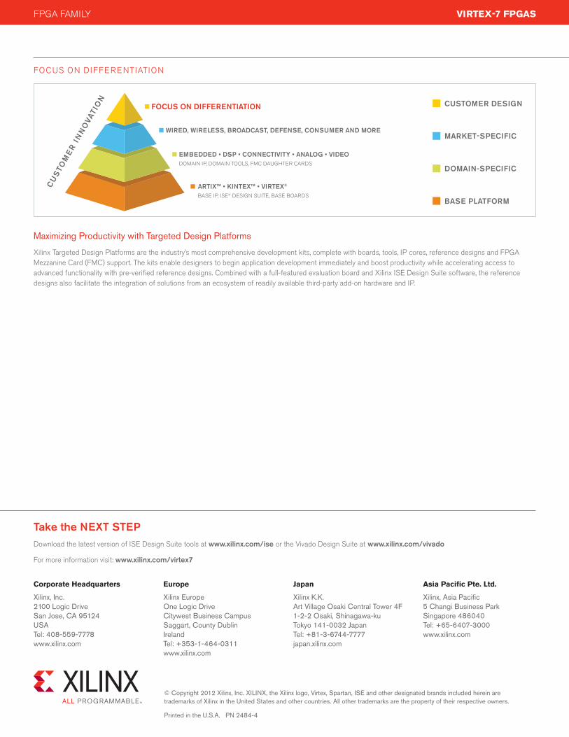
EMBEDDED • DSP • CONNECTIVITY • ANALOG • VIDEODOMAIN IP, DOMAIN TOOLS, FMC DAUGHTER CARDS
ARTIX™ • KINTEX™ • VIRTEX®
BASE IP, ISE® DESIGN SUITE, BASE BOARDS
FOCUS ON DIFFERENTIATION
WIRED, WIRELESS, BROADCAST, DEFENSE, CONSUMER AND MORE
CUSTOMER DESIGN
MARKET-SPECIFIC
DOMAIN-SPECIFIC
BASE PLATFORM
CU
STO
ME
R I
NN
OVA
TIO
N
FOCUS ON DIFFERENTIATION
Maximizing Productivity with Targeted Design Platforms
Xilinx Targeted Design Platforms are the industry’s most comprehensive development kits, complete with boards, tools, IP cores, reference designs and FPGA Mezzanine Card (FMC) support. The kits enable designers to begin application development immediately and boost productivity while accelerating access to advanced functionality with pre-verified reference designs. Combined with a full-featured evaluation board and Xilinx ISE Design Suite software, the reference designs also facilitate the integration of solutions from an ecosystem of readily available third-party add-on hardware and IP.