Embed Size (px)
Citation preview

Chapter 8 − Datapaths Page 1 of 21
Principles of Digital Logic Design Enoch Hwang Last updated 3/3/2003 10:06 AM
Table of Content Table of Content ........................................................................................................................................................... 1 8 Datapaths............................................................................................................................................................... 2
8.1 General Datapath........................................................................................................................................... 3 8.2 Using a General Datapath ............................................................................................................................. 4 8.3 Timing Issues ................................................................................................................................................ 5 8.4 A More Complex Datapath ........................................................................................................................... 8 8.5 VHDL for the Complex Datapath ............................................................................................................... 10 8.6 Dedicated Datapath ..................................................................................................................................... 15 8.7 VHDL for a Dedicated Datapath................................................................................................................. 18 Index ....................................................................................................................................................................... 21

Chapter 8 − Datapaths Page 2 of 21
Principles of Digital Logic Design Enoch Hwang Last updated 3/3/2003 10:06 AM
ControlSignals
StatusSignals
01s y
'0'
DataInputs
DataOutputs
Datapath
ALU
registerff
OutputLogicNext-
stateLogic
ControlInputs
ControlOutputs
StateMemory
register
Control unit
ff
8 Datapaths
So far, we have learned how to design functional units for performing single simple operations such as the ALU for adding two numbers or the comparator for comparing two values. The next logical question to ask is how do we design a circuit for performing more complex operations or operations that involve multiple steps? For example, how do we design a circuit for adding four numbers or a circuit for adding a million numbers? For adding four numbers, we can connect three adders together, but for adding a million numbers, we really don’t want to connect a million minus one adders together. Instead, we want a circuit with just one adder but use it a million times. A datapath circuit allows us to do just that, that is, operations involving multiple steps.
In this chapter, we will look at the design of the datapath. You recall that the datapath is the second main part of a microprocessor. The datapath is responsible for the manipulation of data. It includes (1) functional units such as adders, shifters, multipliers, ALUs, and comparators, (2) registers and other memory elements for the temporary storage of data, and (3) buses and multiplexers for the transfer of data between the different components in the datapath. External data can be entered into the datapath through the data input lines. Results from the computation are provided through the data output lines.
In order for the datapath to function correctly, appropriate control signals must be asserted at the right time. Control signals are needed for all the select and control lines for all the components used in the datapath. This includes all the select lines for multiplexers, ALU and other functional units having multiple operations, all the read/write enable signals for registers and register files, address lines for register files, and enable signals for tri-state buffers. The operation of the datapath is determined by which control signals are asserted and at what time. In a microprocessor, these control signals are generated by the control unit.
In return, the datapath needs to supply status signals back to the control unit in order for it to operate correctly. These status signals are usually from the output of comparators. The comparator tests for a given logical condition between two values. These values can be obtained either from memory elements, directly from the output of functional units, or hardwired as constants. These status signals provide input information for the control unit to determine what operation to perform next. For example, in a conditional loop situation, the status signal will tell the control unit whether to repeat or exit the loop.
Since the datapath performs all the functional operations of a microprocessor, and the microprocessor is for solving problems, therefore the datapath must be able to perform all the operations required to solve the given problem. For example, if the problem requires the addition of two numbers, the datapath, therefore, must contain an adder. If the problem requires the storage of three temporary variables, the datapath must have three registers. However, even with these requirements, there are still many options as to what is actually implemented in the datapath. For example, an adder can be implemented as just a single adder circuit, or as part of the ALU. Registers can be separate register units or combined in a register file. Furthermore, two temporary variables can share the same register if they are not needed at the same time.
Datapath design is also referred to as the register-transfer level (RTL) design. In the register-transfer level design, we look at how data is transferred from one register to another or back to the same register. If the same data is written back to a register without any modifications, then nothing has been accomplished. So before writing the data to a register, the data passes through one or more functional units and gets modified. The time from the reading of the data to the modifying of the data by functional units and finally to the writing of the data back to a register must all happen within one clock cycle.
When designing a datapath to solve a certain problem, there are two methods that can be used. You can start with a general datapath and see if it contains all of the required functional units and enough registers for the problem at hand. Or you can first look at the problem and determine what functional units and how many registers are

Chapter 8 − Datapaths Page 3 of 21
Principles of Digital Logic Design Enoch Hwang Last updated 3/3/2003 10:06 AM
needed, and then create a dedicated or custom datapath just for solving this one problem. We will first look at general datapaths and how to use them and then we will look at the design of dedicated or custom datapaths.
8.1 General Datapath Figure 1 (a) shows an example of a simple general datapath. It contains one functional unit, the ALU, and one
register for storing data. The input to the A operand of the ALU can be either an external input or the constant ‘1’ as selected by the multiplexer select signal line IE. The B operand of the ALU is always from the content of the register. The operation of the ALU is determined by the three control lines ALU2, ALU1, and ALU0, as defined in Figure 1 (b). The design of the ALU was discussed in section 5.2. The register provides a load capability for loading the output of the ALU into the register. The register can also be reset to zero by asserting the Clear signal line. The content of the register can be passed to the external output by asserting the output enable line OE of the tri-state buffer. We assume here that the buses for transferring the data between components are eight bits wide. All the control lines, of course, are one bit.
6
Input
mux01
0
LoadClear Register
2
Clk
543
'1'
IE
OE
1
ALU0
ALU1
ALU2
A B
Output
(a)
Figure 1. A simple datapath: (a) circuit; (b) ALU operations.
There are seven control lines (number 0 to 6) for controlling the operations of this simple datapath. Various operations can be performed by this simple datapath by asserting or de-asserting these control signals at different times. These control lines are grouped together to form what is called a control word. One operation of the datapath, therefore, is determined by the values set in one control word, and will take one clock cycle to perform. By combining multiple control words together in a certain sequence, the datapath will perform the specified operations in the order given.
For example, to load a value from the external input to the register, we would set the control word as follows
IE ALU2 ALU1 ALU0 Load Clear OE Control line 6 5-3 2 1 0 Value set 1 000 (pass) 1 0 0
By setting IE = 1, we select the external input to pass through the mux. From Figure 1 (b), we see that setting the ALU control lines ALU2, ALU1, and ALU0 to 000 selects the pass through operation. Finally, setting Load = 1
ALU2 ALU1 ALU0 Operation 0 0 0 Pass through A 0 0 1 A AND B 0 1 0 A OR B 0 1 1 NOT A 1 0 0 A + B 1 0 1 A – B 1 1 0 A + 1 1 1 1 A – 1
(b)
Chapter 8 − Datapaths Page 4 of 21
Principles of Digital Logic Design Enoch Hwang Last updated 3/3/2003 10:06 AM
loads the value from the output of the ALU into the register. Thus, we have stored the input value into the register. We do not want to output the value from the register so OE is set to 0.
Note that the writing of the register occurs at the next active edge of the clock. Thus, the new value is not available to be read from the register until the next clock cycle. If we had set OE to 1 in the above control word, we would be reading the register in the current clock cycle and thus outputting the original value found in the register rather then the new value that was just entered in.
8.2 Using a General Datapath A general datapath, such as the one described in the previous section, can be used to solve various problems as
long as it has all of the required functional units and has enough registers for storing all the temporary data. The idea of using a general datapath is that we can use a “ready made” circuit to solve a given problem without having to modify it. The trade off is a time versus space issue. On one hand, we do not need the extra time to design a custom or dedicated datapath. On the other hand, the general datapath may contain more features than what the problem requires, so it not only increases the size of the circuit, but also consumes more power. The following example shows how we can use the general datapath from the previous section to solve a problem.
Example 8.1
To see how a datapath is used to perform a computation, let us write the control words for the datapath of Figure 1 (a) to generate and output the numbers from 1 to 10. The algorithm for doing this is shown in Figure 2 (a).
To translate this algorithm to control words for our datapath, we need to look at all the instructions in the algorithm that performs data operations (since this is what the datapath is responsible for); namely, lines 1, 3 and 4. Line 2 is not a data operation instruction but rather a control instruction, even though it reads the value of i. The condition is evaluated by the datapath and a status signal (telling whether the condition is true or false) is generated and sent to the control unit. Depending on this status signal, the control unit will decide whether or not to loop again. The control words for the three instructions are shown in Figure 2 (b).
Figure 2. Generate and output the numbers from 1 to 10: (a) algorithm; (b) control words for the datapath in Figure 1 (a) using three control words.
Control word 1 initializes i to 0. The register in the datapath is used to store the value of i. Since the register has a Clear feature, we can assert this Clear signal to zero the register. The ALU is not needed in this operation so it doesn’t matter what the inputs to the ALU are, or the operation that is selected for the ALU to perform. Hence, the four control lines IE (for selecting the input), and ALU2, ALU1, and ALU0 (for selecting the ALU operation) are all set to ×’s (“don’t cares”). Load is de-asserted because we don’t need to store the output of the ALU to the register. At this time, we also do not want to output the value from the register, so the output control line OE is also de-asserted.
1 i = 02 while (i < 10){3 i = i + 14 output i5 }
(a)
Control IE ALU2 ALU1 ALU0 Load Clear OE Word Instruction 6 5-3 2 1 0
1 i = 0 × ××× 0 1 0 2 i = i + 1 0 100 (add) 1 0 0 3 output i × ××× 0 0 1
(b)

Chapter 8 − Datapaths Page 5 of 21
Principles of Digital Logic Design Enoch Hwang Last updated 3/3/2003 10:06 AM
Control word 2 increments i, so we need to add a one to the value that is stored in the register. Although, the ALU has an increment operation, we cannot use it because the ALU was designed such that the operation increments the A operand rather then the B operand (see Figure 1 (b)), and our datapath is connected such that the output of the register goes to the B operand. Now, we can modify the ALU to have an increment B operation, or we can modify the datapath so that the output of the register can be routed to the A operand of the ALU. However, both of these solutions require the modifications of the datapath, and this defeats the purpose of using a general datapath. Instead, what we can do is to use the ALU add (100) operation to increment the value stored in the register by one. We can get a one to the A operand by setting IE to 0 since the 0 input line of the mux is tied to the constant ‘1’. The B operand will have the register value. Finally, we need to load the result of the ALU back into the register so the Load line is asserted.
Control word 3 outputs the incremented value. Again, we don’t care about the inputs to the ALU and the operation of the ALU, so there is no new value to load into the register. We definitely do not want to clear the register. We simply want to output the value from the register, so we just assert OE by setting it to a 1.
Note that control words 2 and 3 must be executed ten times in order to output the ten numbers. The while loop in the algorithm is implemented in the control unit and we will see in the next chapter how it is done.
The simulation trace of the control words is shown in Figure 3. Notice that two cycles are needed for each count – the first cycle for control word 2 and the second cycle for control word 3. These two cycles are repeated ten times for the ten numbers. For example, at 500ns (at beginning of the first of the two clock cycles), Load = 1 and OE = 0. The current content of the register is 1. Since OE = 0, so the output is Z. At 700ns (the beginning of the second of the two clock cycles), the register is updated with the value 2. Load is de-asserted and OE is asserted, and the number 2 is outputted. ♦
The simulation trace shown in Figure 3 for example 8.1 was obtained by manually asserting and de-asserting the datapath control signals at each clock cycle. This is only because we wanted to test out the datapath and we have not yet constructed the control unit for generating these control signals. What we really need to do is to construct the control unit based on the control words from Figure 2 (b). The control unit will generate the appropriate control signals for the datapath for each clock cycle.
The control unit will also have to determine whether to repeat control words 2 and 3 in the loop, or to terminate. In order for the control unit to know this, we must add a comparator to the output of the register in the datapath to test whether the count is ten or not. The output of this comparator is the status signal that the datapath sends to the control unit.
In the following chapters, you will learn how to construct the control unit and then combine it with the datapath together to form a microprocessor. The resulting microprocessor from example 8.1, of course, will do nothing more than just count from 1 to 10. But with this microprocessor, you wouldn’t have to manually control the datapath control signals as you did in the example.
8.3 Timing Issues One control word is executed in one clock cycle. In one clock cycle, data from a register is first read, then it
passes through functional units and gets modified, and finally it is written back to a register. In example 8.1, two control words are needed for the addition and the output operations. Control word 2 does the addition and writing of the result into the register. Referring to Figure 4, we see that during this clock cycle for control word 2, the operations start with the constant ‘1’ passing down through the mux, follow by the ALU performing the addition. The resulting value from the addition is written to the register at the beginning of the next clock cycle. Recall that this is how the D flip-flop from section 6.7 was constructed – a new value gets latched into the flip-flop at the active edge of the clock. Therefore, the value that is available at the output of the register in the current clock cycle is still the value before the load, which is the value before the increment. If we assert the OE signal in the same clock cycle to output the register value as shown in control word 2 of Figure 5, the output value would be the value before the increment and not the result from after the increment. Because of this, example 8.1 uses control word 3, starting at the next clock cycle, to do the output of the new value.
Performing both a read and a write from/to the same register in the same control word, i.e. same clock cycle, do not create any signal conflict because the reading occurs immediately in the current clock cycle and is getting the original value that is in the register. The writing occurs at the beginning of the next clock cycle after the reading.

Chapter 8 − Datapaths Page 6 of 21
Principles of Digital Logic Design Enoch Hwang Last updated 3/3/2003 10:06 AM
Figure 3. Simulation trace for using three control words as shown in Figure 2(b).
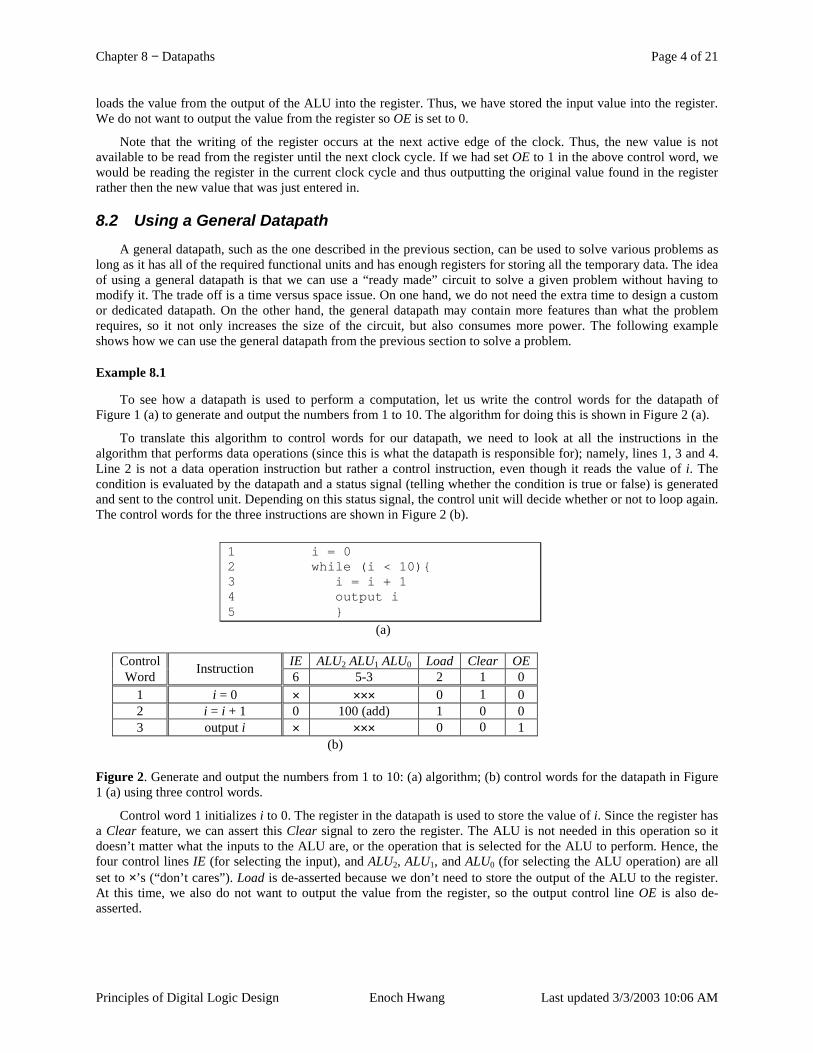
Figure 6 shows the simulation trace for the control words of Figure 5 where the increment and output are both done in control word 2. There are two main differences between this simulation trace and the one from Figure 3. The first is that each count now only requires one clock cycle rather than two. As a result, the time to count to ten is about half (2.4µs versus 4.0µs). The second thing is that the first output value is a zero and not a one as it should be. The first time that control word 2 executes is the clock cycle between 100ns and 300ns. The incremented value (1) does not get written into the register until at 300ns. So when OE is asserted before 300ns, the output value is 0.
We certainly like the fact that it only requires half the time, but outputting a zero at the beginning is not what we wanted. There are several possible solutions, one of which is shown in Figure 7 and Figure 8. OE is not asserted in control word 2 which is executed only once at the start. Subsequent executions of control word 3 will have OE asserted together with the addition and this one we will repeat ten times.
clock signal
Start of controlword 2.
Start of controlword 3.Write register withALU result
Constant '1' passesthrough mux. ALU performs A+B
one clock cycle
Readregister
Figure 4. Read and write timings for a control word.
Control IE ALU2 ALU1 ALU0 Load Clear OE Word Instruction 6 5-3 2 1 0
1 i = 0 × ××× 0 1 0 2 i = i + 1 & output i 0 100 (add) 1 0 1
Figure 5. Counting algorithm using two control words for the datapath in Figure 1(a).
Chapter 8 − Datapaths Page 7 of 21
Principles of Digital Logic Design Enoch Hwang Last updated 3/3/2003 10:06 AM
Figure 6. Simulation trace for using the two control words from Figure 5.
Control IE ALU2 ALU1 ALU0 Load Clear OE Word Instruction 6 5-3 2 1 0
1 i = 0 × ××× 0 1 0 2 i = i + 1 0 100 (add) 1 0 0 3 i = i + 1 & output i 0 100 (add) 1 0 1
Figure 7. Optimized control words for the counting algorithm using the datapath in Figure 1(a).
Figure 8. Corrected simulation trace for using the two control words from Figure 5.

Chapter 8 − Datapaths Page 8 of 21
Principles of Digital Logic Design Enoch Hwang Last updated 3/3/2003 10:06 AM
8.4 A More Complex Datapath When a particular general datapath does not contain all the functional units and/or registers needed to perform
all the required operations specified in the algorithm that you are trying to solve, then you need to select a more complex datapath. When working with general datapaths, the goal is to find the simplest and smallest one that matches the requirements of the problem as close as possible. Example 8.2 shows the need for selecting a more complex datapath.
Example 8.2
As another example, let us use the simple datapath of Figure 1 (a) to generate and add the numbers from n down to 1 where n is an input number, and output the sum of these numbers. The algorithm for doing this is shown in Figure 9 (a). The algorithm requires the use of two variables, n for the input that counts down to zero, and sum for adding up the total. This means that we need two registers in the datapath, unless we want the user to enter the numbers from n down to 1 manually and just use the one register to store the sum. Thus, we conclude that the datapath of Figure 1 (a) cannot be used to implement this algorithm. ♦
In order to implement the algorithm of Figure 9 (a) we need a slightly more complex datapath that includes at least two registers. One possible datapath is shown in Figure 10 (a). The main difference between this datapath and the previous one is that a register file (RF) with four locations is used instead of having just one register. The register file, as discussed in section 7.2, has one write port and two read ports. To access a particular port, the enable line for that port must be asserted and the address for the location set up. The designated lines are WE for write enable, RAE for read A enable, and RBE for read B enable, WA for the write address, RAA for the read A address, and RBA for the read B address. The read ports A and B can be read simultaneously, and they are connected to the two input operands A and B of the ALU respectively. The result of the ALU is passed through a shifter whose operation is specified in Figure 10 (c). Although the shifter is not needed by the algorithm of Figure 9 (a), it is available in this datapath. The output of the shifter is routed back to the register file via the mux or it can be outputted externally by enabling the tri-state buffer. The datapath width is again assumed to be eight bits wide.
1 sum = 02 input n3 while (n ≠ 0){4 sum = sum + n5 n = n - 16 }7 output sum
(a)
Control IE WE WA1,0 RAE RAA1,0 RBE RBA1,0 ALU2,1,0 SH1,0 OE Word Instruction 15 14 13-12 11 10-9 8 7-6 5-3 2-1 0
1 sum = 0 0 1 00 1 00 1 00 101 (subtract) 00 0 2 input n 1 1 01 0 ×× 0 ×× ××× ×× 0 3 sum = sum + n 0 1 00 1 00 1 01 100 (add) 00 0 4 n = n - 1 0 1 01 1 01 0 ×× 111 (decrement) 00 0 5 output sum × 0 ×× 1 00 0 ×× 000 (pass) 00 1
(b) Figure 9. Generate and sum the numbers from n down to 1: (a) algorithm; (b) control words for the datapath in Figure 10.

Chapter 8 − Datapaths Page 9 of 21
Principles of Digital Logic Design Enoch Hwang Last updated 3/3/2003 10:06 AM
ALU0
ALU1
ALU2
A B
15
Input
mux01
WEWA 4x8
RFRAERAA
RBERBA
1413-12
1110-9
87-6
Clk
543
0
IE
OE
ShifterSH1SH0
21
(a)
Figure 10. Complex datapath with register file: (a) circuit; (b) ALU operations; (c) Shifter operations.
Example 8.3
The summation algorithm of Figure 9 (a) can be implemented using the datapath in Figure 10. The control words for manipulating the datapath are shown in Figure 9(b).
Control word 1 initializes sum to 0 by performing a subtraction where the two operands are the same. The location of the register file (RF) used for the two operands is arbitrary because it doesn’t matter what the value is as long as both operands get the same value. We use RF location 0 to store the value of variable sum. Thus, we assert all three RF enable lines and set the RF write address to location 0 and the two RF read addresses also to location 0. The shifter is not needed, so the pass through operation is selected. All the operations specified by a control word are performed within one clock cycle. The timing for the operations of this control word is as follows. At the active edge of the clock, the FSM enters the state for this control word. The appropriate control signals for this control word to the datapath are asserted. Data from RF location 0 is read for both ports and passed to the ALU. Recall that the register file is constructed such that the data from reading a port is available immediately and does not have to wait until the next active clock edge. Since both the ALU and the Shifter are combinational circuits, they will operate within the same clock cycle. The result is written back to RF location 0 at the next active clock edge. Thus, the updated or new value in RF location 0 is not available until the beginning of the next clock cycle.
Control word 2 inputs the value n and stores it in RF location 1. To read from the input, we set IE = 1. To write n into RF location 1 we set WE = 1 and WA = 01. Both the ALU and the shifter are not used in this control word so their select lines are set to don’t cares.
Control word 3 reads sum through port A by setting RAE = 1 and RAA1,0 = 00, and n through port B by setting RBE = 1 and RBA1,0 = 01. These two numbers are added together by setting the ALU select lines to 100. The result of the addition passes through the shifter and the mux, and is written back to RF location 00.
Control word 4 decrements n by 1 by using the decrement operation of the ALU (111). From RF location 01, n is read through port A and passes to the A operand of the ALU. The result is written back to RF location 1.
ALU2 ALU1 ALU0 Operation 0 0 0 Pass through A 0 0 1 A AND B 0 1 0 A OR B 0 1 1 NOT A 1 0 0 A + B 1 0 1 A – B 1 1 0 A + 1 1 1 1 A – 1
(b)
SH1 SH0 Operation 0 0 Pass through 0 1 Shift left and fill with 0 1 0 Shift right and fill with 0 1 1 Rotate right
(c)

Chapter 8 − Datapaths Page 10 of 21
Principles of Digital Logic Design Enoch Hwang Last updated 3/3/2003 10:06 AM
Control word 5 outputs the result that is stored in sum by reading from RF location 0 via port A and passing it through the ALU and shifter. OE is asserted to enable the tri-state buffer for the output.
For the algorithm to be executed automatically, the looping of the control words 3 and 4 must be controlled by the control unit. A comparator that tests for the condition (n ≠ 0) is added to the datapath. This comparator generates the status signal (of whether the condition (n ≠ 0) is true or false) for the control unit to decide whether to repeat the loop or not.
The simulation trace of the control words is shown in Figure 11. Again, the datapath control signals are manually set until n (RF1) reaches 0 at which point OE is asserted and the summation value 55 appears on the output. ♦
Figure 11. Simulation trace for the summation problem control words of Figure 9(b).
8.5 VHDL for the Complex Datapath In modeling the datapath using VHDL, we need to work at the structural level. First, all the components used in
the datapath must be described individually. It doesn’t matter whether they are written at the behavioral, dataflow, or structural level. These components are then connected together in an enclosing module using the structural level method.
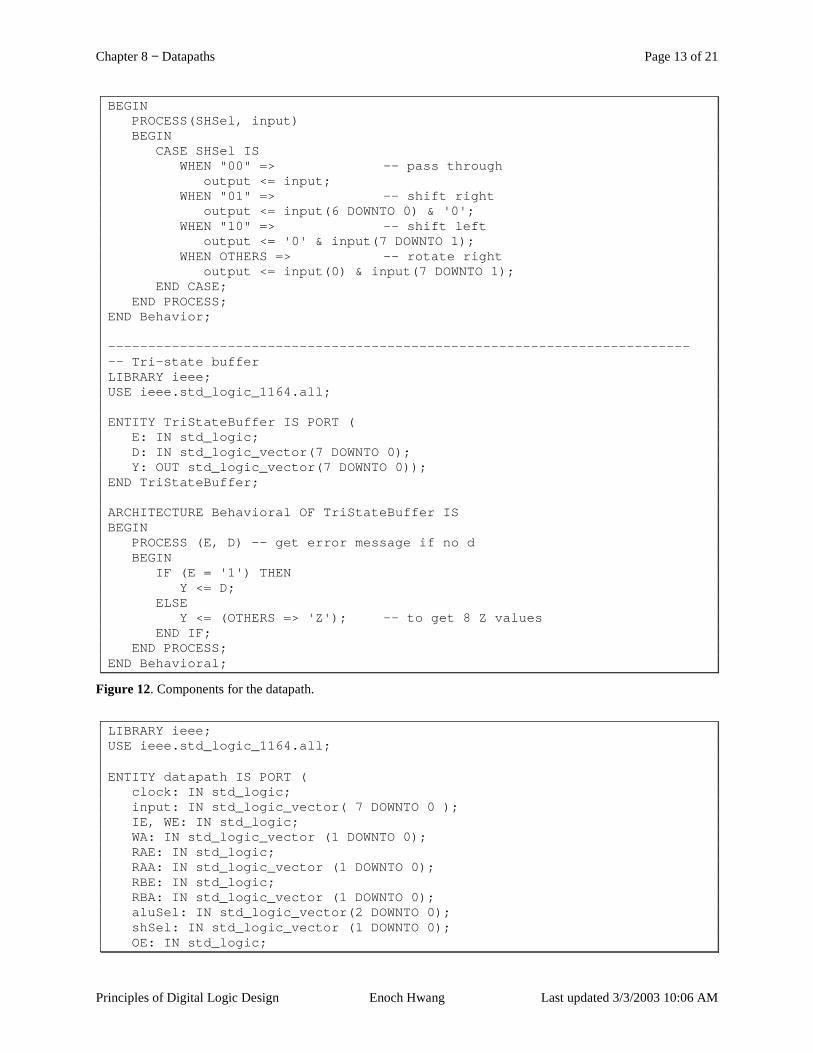
Figure 12 and Figure 13 contain the complete VHDL code for modeling the complex datapath circuit from Figure 10. Figure 12 lists the definitions for all the components used in the datapath. The detail constructions of these components are discussed in previous chapters. Figure 13 shows the enclosing module that combines these components together to form the datapath.
-- 2-to-1 MUXLIBRARY ieee;USE ieee.std_logic_1164.all;
ENTITY mux2 IS PORT (S: IN std_logic; -- select lineD1, D0: IN std_logic_vector(7 downto 0); -- data bus inputY: OUT std_logic_vector(7 downto 0)); -- data bus output
END mux2;

Chapter 8 − Datapaths Page 11 of 21
Principles of Digital Logic Design Enoch Hwang Last updated 3/3/2003 10:06 AM
ARCHITECTURE Behavioral OF mux2 ISBEGIN
PROCESS(S, D1, D0)BEGIN
IF(S = '0' )THENY <= D0;
ELSEY <= D1;
END IF;END PROCESS;
END Behavioral;
--------------------------------------------------------------------------- Register FileLIBRARY ieee;USE ieee.std_logic_1164.all;USE ieee.std_logic_unsigned.all;--USE ieee.std_logic_arith.all;
ENTITY regfile IS PORT (clk: IN std_logic; --clockWE: IN std_logic; --write enableWA: IN std_logic_vector(1 DOWNTO 0); --write addressinput: IN std_logic_vector(7 DOWNTO 0); --inputRAE: IN std_logic; --read enable ports A & BRAA: IN std_logic_vector(1 DOWNTO 0); --read address port A & BRBE: IN std_logic; --read enable ports A & BRBA: IN std_logic_vector(1 DOWNTO 0); --read address port A & BAout, Bout: OUT std_logic_vector(7 DOWNTO 0)); --output port A & B
END regfile;
ARCHITECTURE Behavioral OF regfile ISSUBTYPE reg IS std_logic_vector(7 DOWNTO 0);TYPE regArray IS array(0 TO 3) OF reg;SIGNAL RF: regArray; --register file contents
BEGINWritePort: PROCESS (clk)BEGIN
IF (clk'EVENT AND clk = '1') THENIF (WE = '1') THEN
RF(CONV_INTEGER(WA)) <= input;END IF;
END IF;END PROCESS;
ReadPortA: PROCESS (RAE, RAA)BEGIN
IF (RAE = '1') thenAout <= RF(CONV_INTEGER(RAA)); -- convert bit VECTOR to integer
ELSEAout <= (others => 'Z');
END IF;END PROCESS;
ReadPortB: PROCESS (RBE, RBA)BEGIN
IF (RBE = '1') then
Chapter 8 − Datapaths Page 12 of 21
Principles of Digital Logic Design Enoch Hwang Last updated 3/3/2003 10:06 AM
Bout <= RF(CONV_INTEGER(RBA)); -- convert bit VECTOR to integerELSE
Bout <= (others => 'Z');END IF;
END PROCESS;END Behavioral;
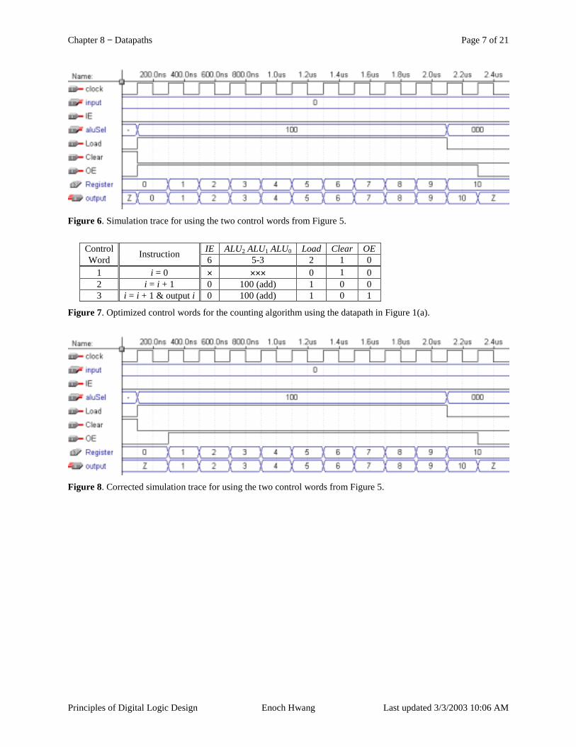
--------------------------------------------------------------------------- ALULIBRARY ieee;USE ieee.std_logic_1164.all;-- need the following to perform arithmetics on std_logic_vectorsUSE ieee.std_logic_unsigned.all;
ENTITY alu IS PORT (ALUSel: IN std_logic_vector(2 DOWNTO 0); -- select for operationsA, B: IN std_logic_vector(7 DOWNTO 0); -- input operandsF: OUT std_logic_vector(7 DOWNTO 0)); -- output
END alu;
ARCHITECTURE Behavior OF alu ISBEGIN
PROCESS(ALUSel, A, B)BEGIN
CASE ALUSel ISWHEN "000" => -- pass A through
F <= A;WHEN "001" => -- AND
F <= A AND B;WHEN "010" => -- OR
F <= A OR B;WHEN "011" => -- NOT
F <= NOT A;WHEN "100" => -- add
F <= A + B;WHEN "101" => -- subtract
F <= A - B;WHEN "110" => -- increment
F <= A + 1;WHEN others => -- decrement
F <= A - 1;END CASE;
END PROCESS;END Behavior;
--------------------------------------------------------------------------- ShifterLIBRARY ieee;USE ieee.std_logic_1164.all;
ENTITY shifter IS PORT (SHSel: IN std_logic_vector(1 DOWNTO 0); -- select for operationsinput: IN std_logic_vector(7 DOWNTO 0); -- input operandsoutput: OUT std_logic_vector(7 DOWNTO 0)); -- output
END shifter;
ARCHITECTURE Behavior OF shifter IS
Chapter 8 − Datapaths Page 13 of 21
Principles of Digital Logic Design Enoch Hwang Last updated 3/3/2003 10:06 AM
BEGINPROCESS(SHSel, input)BEGIN
CASE SHSel ISWHEN "00" => -- pass through
output <= input;WHEN "01" => -- shift right
output <= input(6 DOWNTO 0) & '0';WHEN "10" => -- shift left
output <= '0' & input(7 DOWNTO 1);WHEN OTHERS => -- rotate right
output <= input(0) & input(7 DOWNTO 1);END CASE;
END PROCESS;END Behavior;
--------------------------------------------------------------------------- Tri-state bufferLIBRARY ieee;USE ieee.std_logic_1164.all;
ENTITY TriStateBuffer IS PORT (E: IN std_logic;D: IN std_logic_vector(7 DOWNTO 0);Y: OUT std_logic_vector(7 DOWNTO 0));
END TriStateBuffer;
ARCHITECTURE Behavioral OF TriStateBuffer ISBEGIN
PROCESS (E, D) -- get error message if no dBEGIN
IF (E = '1') THENY <= D;
ELSEY <= (OTHERS => 'Z'); -- to get 8 Z values
END IF;END PROCESS;
END Behavioral;
Figure 12. Components for the datapath.
LIBRARY ieee;USE ieee.std_logic_1164.all;
ENTITY datapath IS PORT (clock: IN std_logic;input: IN std_logic_vector( 7 DOWNTO 0 );IE, WE: IN std_logic;WA: IN std_logic_vector (1 DOWNTO 0);RAE: IN std_logic;RAA: IN std_logic_vector (1 DOWNTO 0);RBE: IN std_logic;RBA: IN std_logic_vector (1 DOWNTO 0);aluSel: IN std_logic_vector(2 DOWNTO 0);shSel: IN std_logic_vector (1 DOWNTO 0);OE: IN std_logic;

Chapter 8 − Datapaths Page 14 of 21
Principles of Digital Logic Design Enoch Hwang Last updated 3/3/2003 10:06 AM
output: OUT std_logic_vector(7 DOWNTO 0));END datapath;
ARCHITECTURE Structural OF datapath IS
COMPONENT mux2 PORT (S: IN std_logic; -- select linesD1, D0: IN std_logic_vector(7 DOWNTO 0); -- data bus inputY: OUT std_logic_vector(7 DOWNTO 0)); -- data bus output
END COMPONENT;
COMPONENT regfile PORT (clk: IN std_logic; --clockWE: IN std_logic; --write enableWA: IN std_logic_vector(1 DOWNTO 0); --write addressinput: IN std_logic_vector(7 DOWNTO 0); --inputRAE: IN std_logic; --read enable ports A & BRAA: IN std_logic_vector(1 DOWNTO 0); --read address port A & BRBE: IN std_logic; --read enable ports A & BRBA: IN std_logic_vector(1 DOWNTO 0); --read address port A & BAout, Bout: OUT std_logic_vector(7 DOWNTO 0)); --output port A & B
END COMPONENT;
COMPONENT alu PORT (ALUSel: IN std_logic_vector(2 DOWNTO 0); -- select for operationsA, B: IN std_logic_vector(7 DOWNTO 0); -- input operandsF: OUT std_logic_vector(7 DOWNTO 0)); -- output
END COMPONENT;
COMPONENT shifter PORT (SHSel: IN std_logic_vector(1 DOWNTO 0); -- select for operationsinput: IN std_logic_vector(7 DOWNTO 0); -- input operandsoutput: OUT std_logic_vector(7 DOWNTO 0)); -- output
END COMPONENT;
COMPONENT tristatebuffer PORT (E: IN std_logic;D: IN std_logic_vector(7 downto 0);Y: OUT std_logic_vector(7 downto 0));
END COMPONENT;
SIGNAL muxout, rfAout, rfBout: std_logic_vector( 7 DOWNTO 0 );SIGNAL aluout, shiftout, tristateout: std_logic_vector( 7 DOWNTO 0 );
BEGIN-- doing structural modeling here
U0: mux2 PORT MAP( IE, input, shiftout, muxout );U1: regfile PORT MAP(clock,WE,WA,muxout,RAE,RAA,RBE,RBA,rfAout,rfBout );U2: alu PORT MAP( ALUsel, rfAout, rfBout, aluout );U3: shifter PORT MAP(SHSel,aluout,shiftout);U4: tristatebuffer PORT MAP(OE, shiftout, tristateout);output <= tristateout;
END Structural;
Figure 13. Datapath constructed at the structural level.
Chapter 8 − Datapaths Page 15 of 21
Principles of Digital Logic Design Enoch Hwang Last updated 3/3/2003 10:06 AM
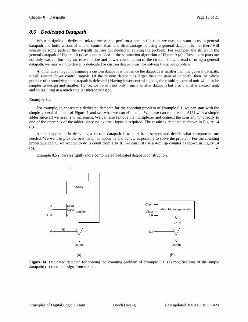
8.6 Dedicated Datapath When designing a dedicated microprocessor to perform a certain function, we may not want to use a general
datapath and build a control unit to control that. The disadvantage of using a general datapath is that there will usually be some parts in the datapath that are not needed in solving the problem. For example, the shifter in the general datapath of Figure 10 (a) was not needed in the summation algorithm of Figure 9 (a). These extra parts are not only wasted, but they increase the size and power consumption of the circuit. Thus, instead of using a general datapath, we may want to design a dedicated or custom datapath just for solving the given problem.
Another advantage in designing a custom datapath is that since the datapath is smaller than the general datapath, it will require fewer control signals. (If the custom datapath is larger than the general datapath, then the whole purpose of customizing the datapath is defeated.) Having fewer control signals, the resulting control unit will also be simpler to design and smaller. Hence, we benefit not only from a smaller datapath but also a smaller control unit, and so resulting in a much smaller microprocessor.
Example 8.4
For example, to construct a dedicated datapath for the counting problem of Example 8.1, we can start with the simple general datapath of Figure 1 and see what we can eliminate. Well, we can replace the ALU with a simple adder since all we need is to increment. We can also remove the multiplexer and connect the constant ‘1’ directly to one of the operands of the adder, since no external input is required. The resulting datapath is shown in Figure 14 (a).
Another approach in designing a custom datapath is to start from scratch and decide what components are needed. We want to pick the best match components and as few as possible to solve the problem. For the counting problem, since all we wanted to do is count from 1 to 10, we can just use a 4-bit up counter as shown in Figure 14 (b). ♦
Example 8.5 shows a slightly more complicated dedicated datapath construction.
0
LoadClear Register
2
Clk
'1'
OE
1
Output
Adder
ClkClear
4-bit binary up counter
Q
4
Count
OE
Output
(a) (b)
Figure 14. Dedicated datapath for solving the counting problem of Example 9.1: (a) modifications of the simple datapath; (b) custom design from scratch.

Chapter 8 − Datapaths Page 16 of 21
Principles of Digital Logic Design Enoch Hwang Last updated 3/3/2003 10:06 AM
Example 8.5
This example designs a dedicated datapath for evaluating the factorial of n. The factorial of n is defined to be the product of 1 × 2 × 3 × … × n. Figure 15 shows the algorithm for solving the factorial of n where n is a user input number.
From analyzing the algorithm, we conclude that the following registers and functional units are needed in the datapath:
• One register for storing the variable product. • One down counter with parallel load for storing the variable n and for decrementing n. The parallel load
feature will allow for the input of n. • One multiply functional unit. • One greater-than-one comparator for returning the status signal to the control unit. • A tri-state buffer for output.
Having decided on what components are needed in the datapath, we need to connect them together so that the functional units will get the correct data, and the outputs from the functional units will be stored in the correct register.
The complete custom datapath is shown in Figure 16. For example, in line 4 of the algorithm, one operand of the multiply function is the product and the other operand is n. Hence, the output of the register where product is stored is connected to one input of the multiply unit. Since n is stored in the counter, therefore, the output of the counter is connected to the second input of the multiply unit. The result of the multiply is assigned back into the variable product. Thus, in the datapath, we needed a connection from the output of the multiply functional unit back to the input of the register where product is stored. However, we cannot make this connection directly because we also need to load the constant 1 into this register as required by line 2 of the algorithm. So a 2-to-1 multiplexer is used to select whether the constant 1 or the output from the multiply unit gets stored in the register. The down counter allows for the execution of line 5. Since the counter also serves as the register for the variable n, we don’t need an extra register. The parallel load feature of the counter allows the execution of line 1. The tri-state buffer, connected to the output of the product register, is needed for the final output of the result. Finally, the comparator generates the status signal for the condition n > 1 to the control unit. One input to the comparator comes from the counter where n is stored and the other input is the constant 1. ♦
1 input n2 product = 13 while n > 14 product = product * n5 n = n – 16 output product
Figure 15 Algorithm for solving the factorial of n.

Chapter 8 − Datapaths Page 17 of 21
Principles of Digital Logic Design Enoch Hwang Last updated 3/3/2003 10:06 AM
*>
"1"
01s y
"1"Input
n > 1
Output
Done
Done
Count
Load
down counteralso for storing n
register forstoring product
Figure 16. Dedicated datapath for solving the factorial of n problem.
When designing a datapath, all the components in the datapath do not have to be interconnected. The datapath can consist of two or more totally disjoint circuits as portray in Example 8.6.
Example 8.6
In this example, we want to construct a custom datapath for solving the following problem:
Input an 8-bit number. Output a 1 if the number has the same number of 0’s and 1’s, otherwise, output a 0. e.g. the number 10111011 will produce a 0 output, whereas, the number 10100011 will produce a 1 output.
The algorithm for solving the problem is shown in Figure 17.
input ncountbit = 0 // for counting the number of zero and one bitscounteight = 0 // for looping eight times
while counteight ≠ 8 {if LSB(n) = 1 // least significant bit of n
countbit = countbit + 1else
countbit = countbit - 1n = n >> 1 // shift n right one bitcounteight = counteight + 1;}
if countbit = 0 thenoutput 1
elseoutput 0
assert Done
Figure 17. Algorithm for solving the problem in Example 8.6.
The functional units and registers required by the custom datapath are as follows:

Chapter 8 − Datapaths Page 18 of 21
Principles of Digital Logic Design Enoch Hwang Last updated 3/3/2003 10:06 AM
• A shifter with parallel load register for storing n. • One 4-bit up/down counter for countbit. • One 3-bit down counter for counteight. • A “not equal to 8” comparator for looping eight times. • An “equal to 0” comparator for testing with countbit.
The schematic for the datapath is shown in Figure 18. Notice that there are no connections between the shifter and the counter. These two forms two completely separate circuits.
To extract the least significant bit of n and test whether it is equal to a 1 or not, we only have to connect to the least significant bit of the shifter and no active component is necessary. To test for counteight ≠ 8, we use a 4-input NAND gate with the least three significant input bits inverted. When the counteight is equal to eight, the NAND gate outputs a 0, which serves as the ending loop condition. Whether the 1 is actually outputted will depend on whether the tri-state buffer is enabled or not. When the control unit asserts the OutDone line to enable the tri-state buffer, this 1 signal can also serve as the Done signal to inform the external user that the computation is completed. In other words, when the Done signal is asserted, the output value is the result of the computation.
shifter withload
countercountbit
Output
OutDone
LSB = 1
DownClear
Input
Done
LoadShift
LSB
Count
Clock
countercounteightDown
Clear
Count
Clock
counteight ≠ 8
Figure 18. The custom datapath for Example 8.6.
8.7 VHDL for a Dedicated Datapath Fig show the VHDL code for the dedicated datapath of Figure 18.
LIBRARY ieee;USE ieee.std_logic_1164.ALL;USE ieee.std_logic_arith.ALL;
ENTITY Datapath IS PORT (Clock: IN STD_LOGIC;
-- primary datapath inputInput: IN STD_LOGIC_VECTOR(7 DOWNTO 0);

Chapter 8 − Datapaths Page 19 of 21
Principles of Digital Logic Design Enoch Hwang Last updated 3/3/2003 10:06 AM
-- control signalsShift: IN STD_LOGIC;Load: IN STD_LOGIC;Countbit: IN STD_LOGIC;Down: IN STD_LOGIC;Counteight: IN STD_LOGIC;Clear: IN STD_LOGIC;Done: IN STD_LOGIC;
-- status signalsEq8: OUT STD_LOGIC;LSBeg1: OUT STD_LOGIC;
-- primary datapath outputOutput: OUT STD_LOGIC);
END Datapath;
ARCHITECTURE Structural OF Datapath ISCOMPONENT shiftreg PORT (
Clock: IN STD_LOGIC;SHSel: IN STD_LOGIC_VECTOR(1 DOWNTO 0);D: IN STD_LOGIC_VECTOR(7 DOWNTO 0);Q: OUT STD_LOGIC_VECTOR(7 DOWNTO 0));
END COMPONENT;
COMPONENT counter PORT (Clock: IN STD_LOGIC;Clear: IN STD_LOGIC;Count: IN STD_LOGIC;Down: IN STD_LOGIC;Q: OUT INTEGER RANGE 0 TO 15);
END COMPONENT;
SIGNAL SHSel: STD_LOGIC_VECTOR(1 DOWNTO 0);SIGNAL ShiftOut: STD_LOGIC_VECTOR(7 DOWNTO 0);SIGNAL CountbitOut: INTEGER RANGE 0 TO 15;SIGNAL CounteightOut: INTEGER RANGE 0 TO 15;SIGNAL Equal: STD_LOGIC;SIGNAL Up: STD_LOGIC;
BEGIN
SHSel <= Shift & Load;U0: shiftreg PORT MAP(Clock,SHSel,Input,ShiftOut);LSBeg1 <= ShiftOut(0);
-- counter for countbitU1: counter PORT MAP(Clock,Clear,Countbit,Down,CountbitOut);Equal <= '1' WHEN CountbitOut = 0 ELSE '0';Output <= Equal WHEN Done = '1' ELSE 'Z';
-- counter for counteightUp <= '0';U2: counter PORT MAP(Clock,Clear,Counteight,Up,CounteightOut);Eq8 <= '1' WHEN CounteightOut = 8 ELSE '0';
END Structural;
Figure 19. VHDL code for the datapath of Example 8.6, Figure 18.

Chapter 8 − Datapaths Page 20 of 21
Principles of Digital Logic Design Enoch Hwang Last updated 3/3/2003 10:06 AM

Chapter 8 − Datapaths Page 21 of 21
Principles of Digital Logic Design Enoch Hwang Last updated 3/3/2003 10:06 AM
Index
C
Control signal, 2, 3 Control word, 3 Custom datapath, 15
D
Datapath, 2 timing issues, 5
Dedicated datapath, 15
G
General datapath, 3
using a, 4
R
Register transfer level, 2 RTL. See Register transfer level.
S
Status signal, 2, 5
T
Timing issues, 5