Embed Size (px)
Citation preview
Chapter 7: BJT Transistor Modeling
Robert BoylestadDigital Electronics
Copyright ©2002 by Pearson Education, Inc.Upper Saddle River, New Jersey 07458
All rights reserved.
Slide 1
Robert BoylestadDigital Electronics
Copyright ©2002 by Pearson Education, Inc.Upper Saddle River, New Jersey 07458
All rights reserved.
Transistor Modeling
A model is an equivalent circuit that represents the AC characteristics of the transistor.It uses circuit elements that approximate the behavior of the transistor.
There are 2 models commonly used in small signal AC analysis of a transistor:
• re model• hybrid equivalent model
Slide 2
Robert BoylestadDigital Electronics
Copyright ©2002 by Pearson Education, Inc.Upper Saddle River, New Jersey 07458
All rights reserved.
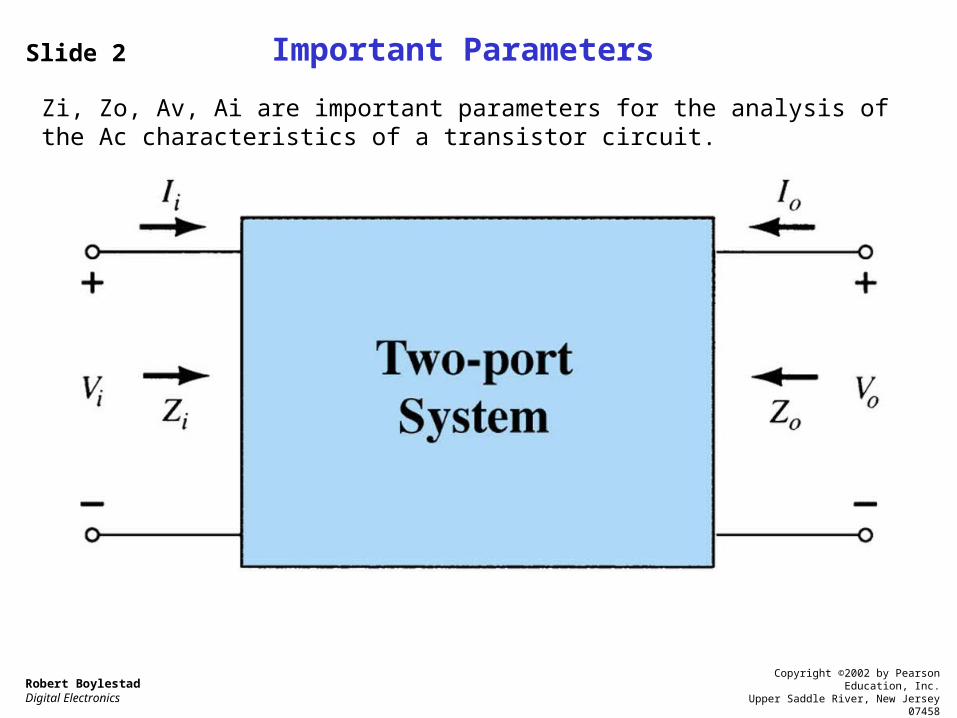
Important Parameters
Zi, Zo, Av, Ai are important parameters for the analysis of the Ac characteristics of a transistor circuit.
Slide 3
Robert BoylestadDigital Electronics
Copyright ©2002 by Pearson Education, Inc.Upper Saddle River, New Jersey 07458
All rights reserved.
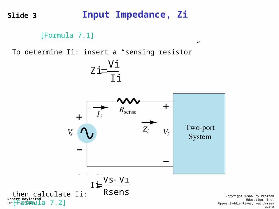
Input Impedance, Zi[Formula
7.1]
To determine Ii: insert a “sensing resistor”
then calculate Ii: [Formula 7.2]
Ii
ViZi
Rsense
ViVsIi
Slide 4
Robert BoylestadDigital Electronics
Copyright ©2002 by Pearson Education, Inc.Upper Saddle River, New Jersey 07458
All rights reserved.
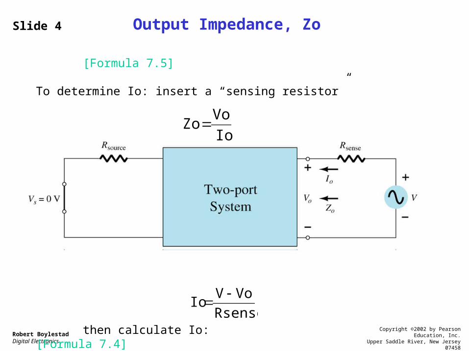
Output Impedance, Zo
[Formula 7.5]
To determine Io: insert a “sensing resistor”
then calculate Io: [Formula 7.4]
Io
VoZo
Rsense
VoVIo
Slide 5
Robert BoylestadDigital Electronics
Copyright ©2002 by Pearson Education, Inc.Upper Saddle River, New Jersey 07458
All rights reserved.
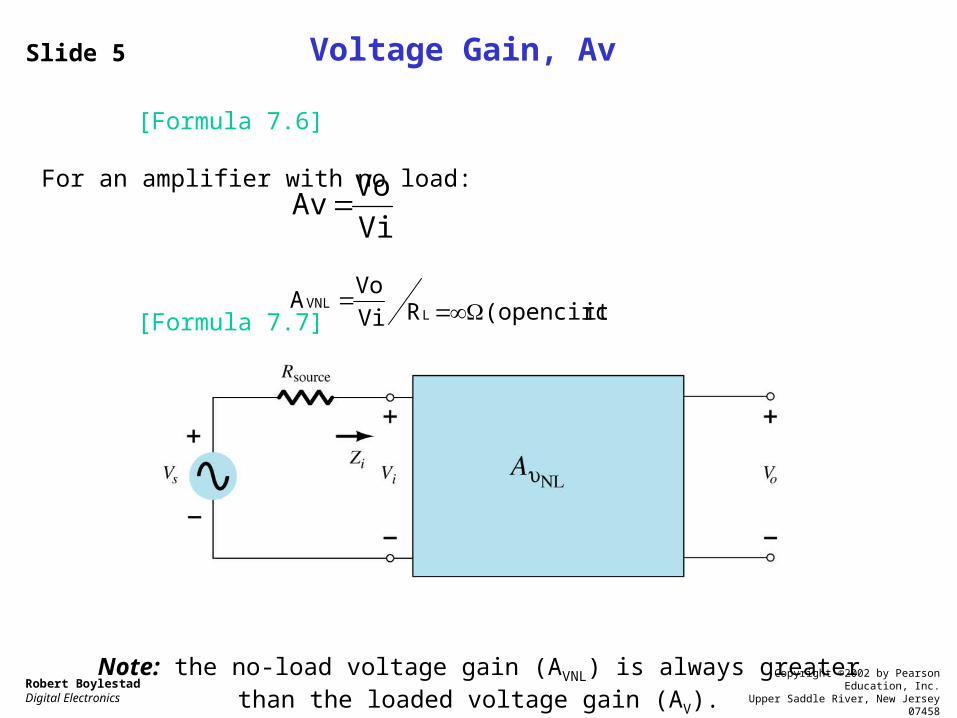
Voltage Gain, Av[Formula
7.6]
For an amplifier with no load:
[Formula 7.7]
Note: the no-load voltage gain (AVNL) is always greaterthan the loaded voltage gain (AV).
Vi
VoAv
it)(opencircuRVi
VoA
LVNL
Slide 6
Robert BoylestadDigital Electronics
Copyright ©2002 by Pearson Education, Inc.Upper Saddle River, New Jersey 07458
All rights reserved.
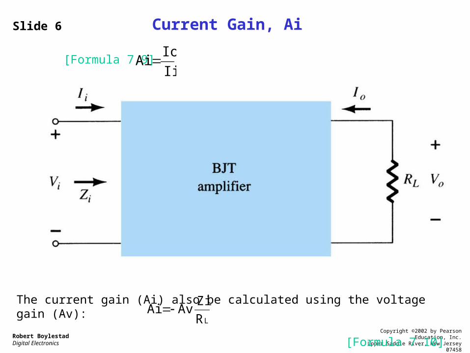
Current Gain, Ai[Formula
7.9]
The current gain (Ai) also be calculated using the voltage gain (Av):
[Formula 7.10]
Ii
IoAi
LR
ZiAvAi
Slide 7
Robert BoylestadDigital Electronics
Copyright ©2002 by Pearson Education, Inc.Upper Saddle River, New Jersey 07458
All rights reserved.
Phase Relationship
The phase relationship between input and output depends on the amplifier configuration circuit.
Common – Emitter ~ 180 degrees
Common - Base ~ 0 degrees
Common – Collector ~ 0 degrees
Slide 8
Robert BoylestadDigital Electronics
Copyright ©2002 by Pearson Education, Inc.Upper Saddle River, New Jersey 07458
All rights reserved.
re Transistor Model
BJTs are basically current controlled devices, therefore the re model uses a diode and a current source to duplicate the behavior of the transistor.
One disadvantage to this model is its sensitivity to the DC level. This model is designed for specific circuit conditions.
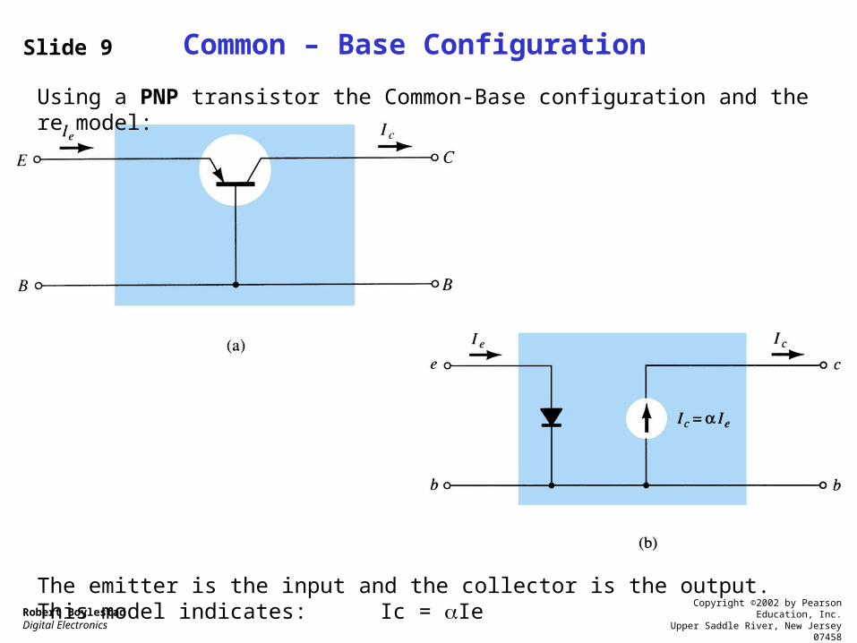
Using a PNP transistor the Common-Base configuration and the re model:
The emitter is the input and the collector is the output.This model indicates: Ic = Ie
Slide 9
Robert BoylestadDigital Electronics
Copyright ©2002 by Pearson Education, Inc.Upper Saddle River, New Jersey 07458
All rights reserved.
Common – Base Configuration
Slide 10
Robert BoylestadDigital Electronics
Copyright ©2002 by Pearson Education, Inc.Upper Saddle River, New Jersey 07458
All rights reserved.
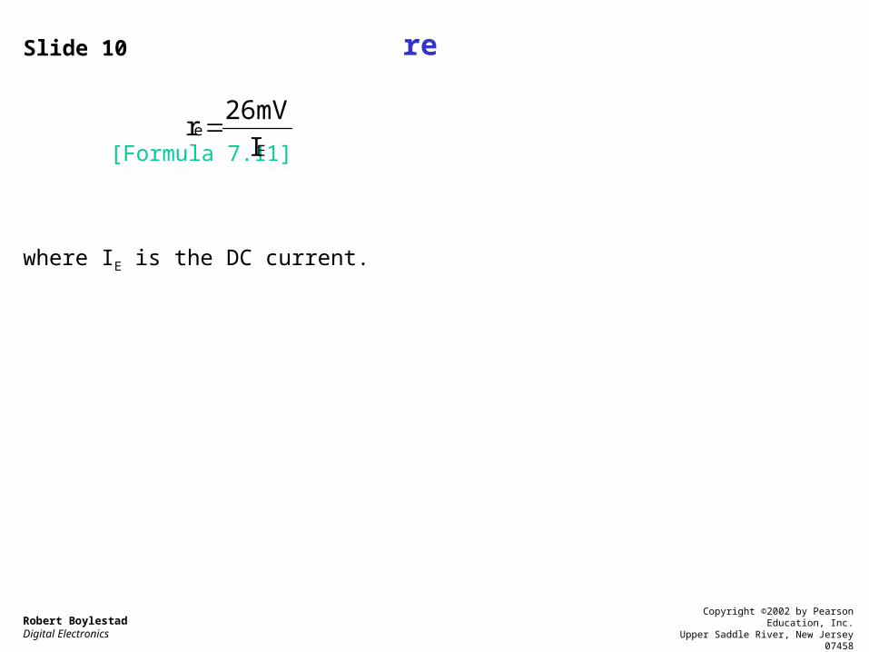
re
[Formula 7.11]
where IE is the DC current.
Ee
I
26mVr
Slide 11
Robert BoylestadDigital Electronics
Copyright ©2002 by Pearson Education, Inc.Upper Saddle River, New Jersey 07458
All rights reserved.
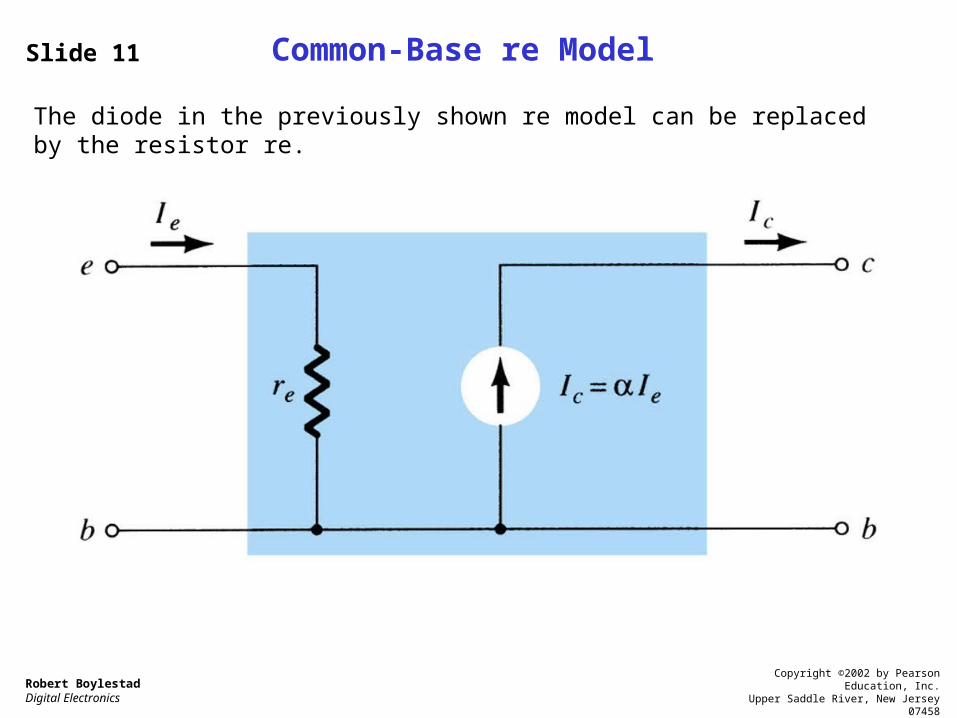
Common-Base re Model
The diode in the previously shown re model can be replaced by the resistor re.
Slide 12
Robert BoylestadDigital Electronics
Copyright ©2002 by Pearson Education, Inc.Upper Saddle River, New Jersey 07458
All rights reserved.
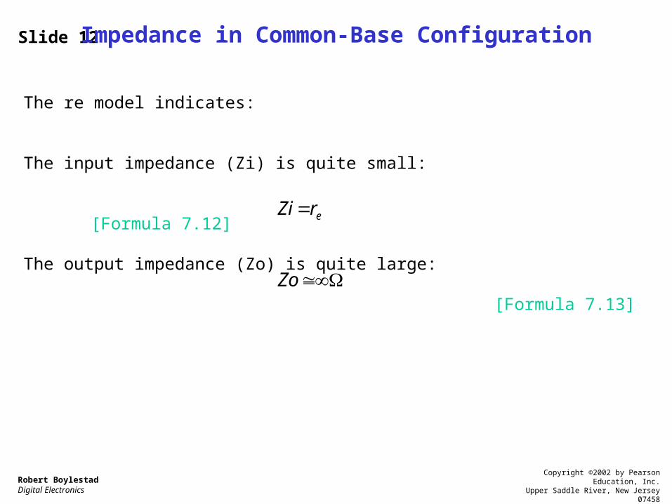
Impedance in Common-Base Configuration
The re model indicates:
The input impedance (Zi) is quite small:
[Formula 7.12]
The output impedance (Zo) is quite large:
[Formula 7.13]
erZi
Zo
Slide 13
Robert BoylestadDigital Electronics
Copyright ©2002 by Pearson Education, Inc.Upper Saddle River, New Jersey 07458
All rights reserved.
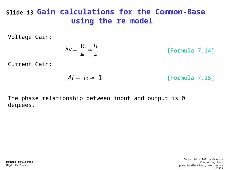
Gain calculations for the Common-Base using the re model
Voltage Gain:
[Formula 7.14]
Current Gain:
[Formula 7.15]
The phase relationship between input and output is 0 degrees.
e
L
e
L
r
R
r
RAv
1 Ai
Slide 14
Robert BoylestadDigital Electronics
Copyright ©2002 by Pearson Education, Inc.Upper Saddle River, New Jersey 07458
All rights reserved.
NPN Common-Base Configuration
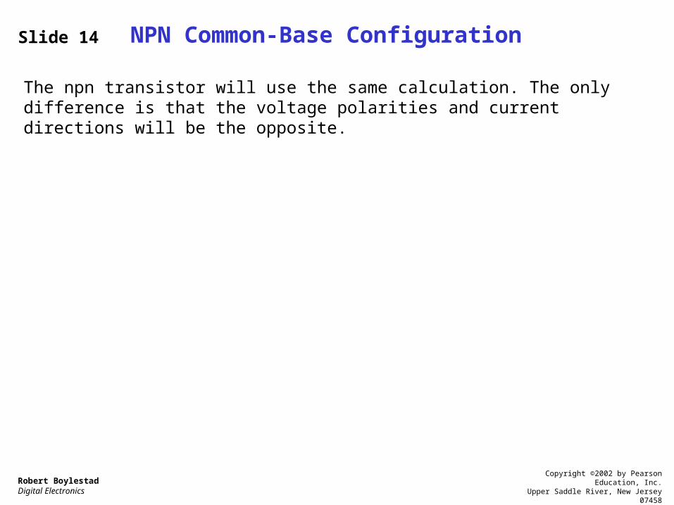
The npn transistor will use the same calculation. The only difference is that the voltage polarities and current directions will be the opposite.
Slide 15
Robert BoylestadDigital Electronics
Copyright ©2002 by Pearson Education, Inc.Upper Saddle River, New Jersey 07458
All rights reserved.
Common-Emitter Configuration
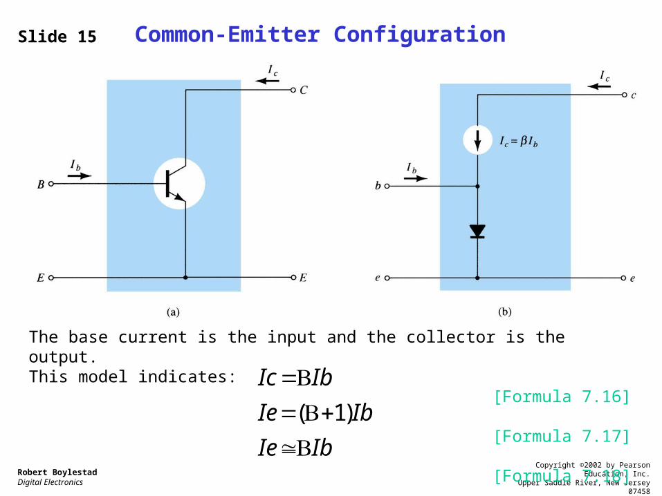
The base current is the input and the collector is the output.This model indicates:
[Formula 7.16]
[Formula 7.17]
[Formula 7.18]IbIe
IbIe
IbIc
)1(
Slide 16
Robert BoylestadDigital Electronics
Copyright ©2002 by Pearson Education, Inc.Upper Saddle River, New Jersey 07458
All rights reserved.
Impedance in Common-Emitter Configuration
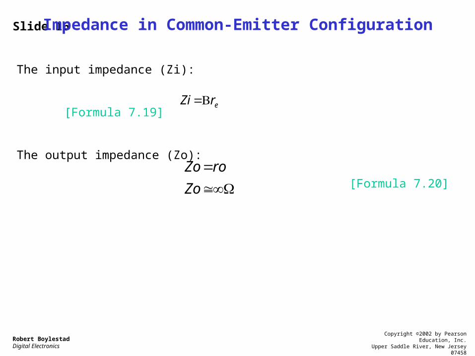
The input impedance (Zi):
[Formula 7.19]
The output impedance (Zo):
[Formula 7.20]
erZi
Zo
roZo
Slide 17
Robert BoylestadDigital Electronics
Copyright ©2002 by Pearson Education, Inc.Upper Saddle River, New Jersey 07458
All rights reserved.
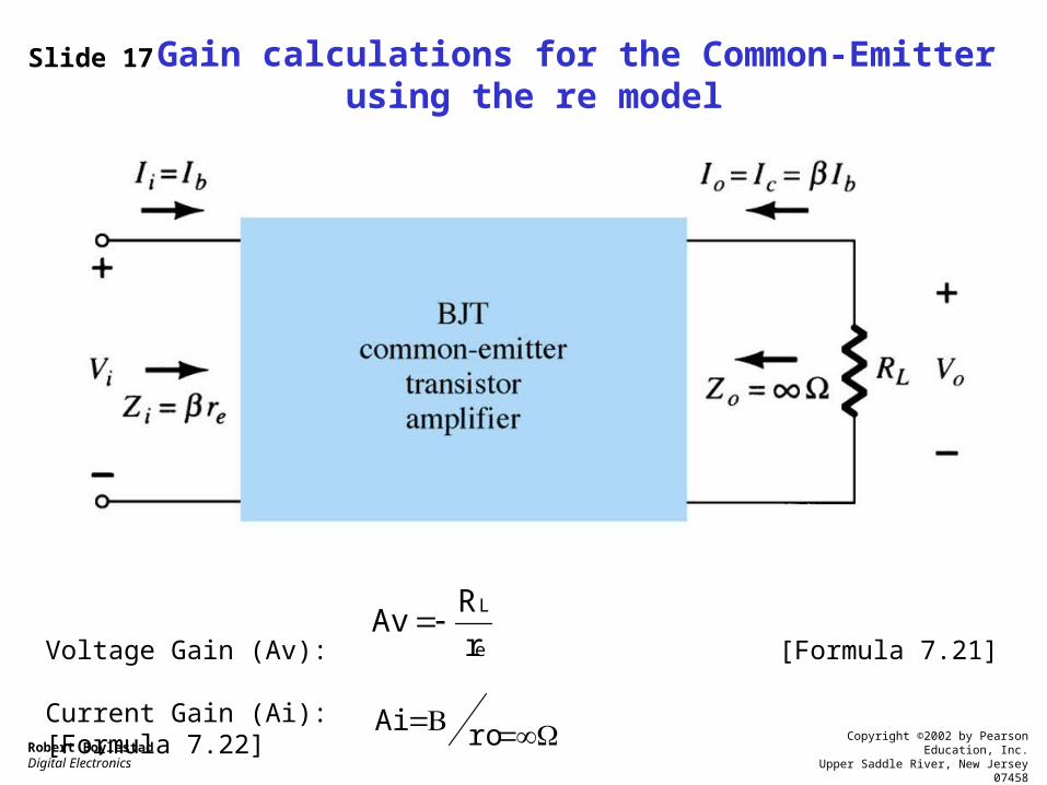
Gain calculations for the Common-Emitter using the re model
Voltage Gain (Av): [Formula 7.21]
Current Gain (Ai): [Formula 7.22]
e
L
r
RAv
roAi
Slide 18
Robert BoylestadDigital Electronics
Copyright ©2002 by Pearson Education, Inc.Upper Saddle River, New Jersey 07458
All rights reserved.
Common-Collector Configuration
The Common-Emitter Model is used for Common-Collector.
Slide 19
Robert BoylestadDigital Electronics
Copyright ©2002 by Pearson Education, Inc.Upper Saddle River, New Jersey 07458
All rights reserved.
Hybrid Equivalent Model
The hybrid parameters: hie, hre, hfe, hoe are developed and used to model the transistor. These parameters can be found in a specification sheet for a transistor.
Slide 20
Robert BoylestadDigital Electronics
Copyright ©2002 by Pearson Education, Inc.Upper Saddle River, New Jersey 07458
All rights reserved.
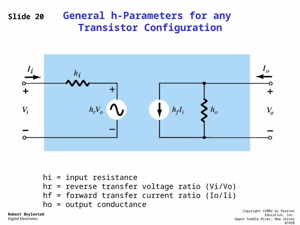
General h-Parameters for any Transistor Configuration
hi = input resistancehr = reverse transfer voltage ratio (Vi/Vo)hf = forward transfer current ratio (Io/Ii)ho = output conductance
Slide 21
Robert BoylestadDigital Electronics
Copyright ©2002 by Pearson Education, Inc.Upper Saddle River, New Jersey 07458
All rights reserved.
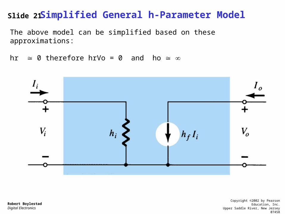
Simplified General h-Parameter Model
The above model can be simplified based on these approximations:
hr 0 therefore hrVo = 0 and ho
Slide 22
Robert BoylestadDigital Electronics
Copyright ©2002 by Pearson Education, Inc.Upper Saddle River, New Jersey 07458
All rights reserved.
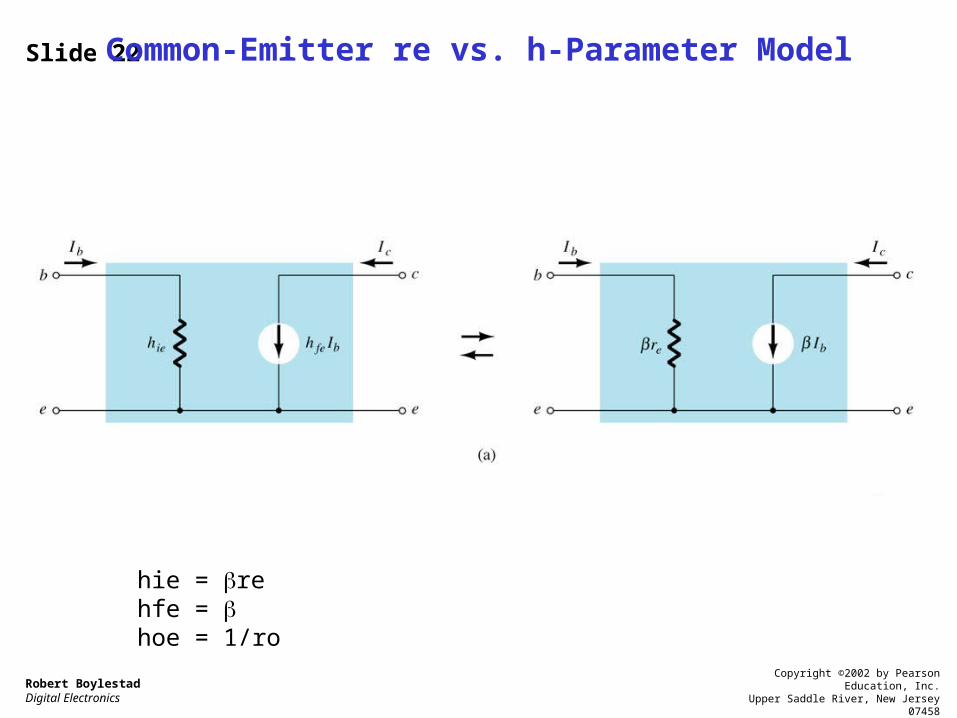
Common-Emitter re vs. h-Parameter Model
hie = rehfe = hoe = 1/ro
Slide 23
Robert BoylestadDigital Electronics
Copyright ©2002 by Pearson Education, Inc.Upper Saddle River, New Jersey 07458
All rights reserved.
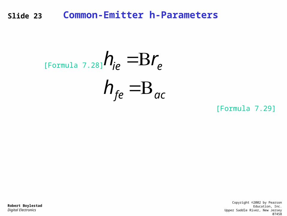
Common-Emitter h-Parameters
[Formula 7.28]
[Formula 7.29]
acfe
eie
h
rh
Slide 24
Robert BoylestadDigital Electronics
Copyright ©2002 by Pearson Education, Inc.Upper Saddle River, New Jersey 07458
All rights reserved.
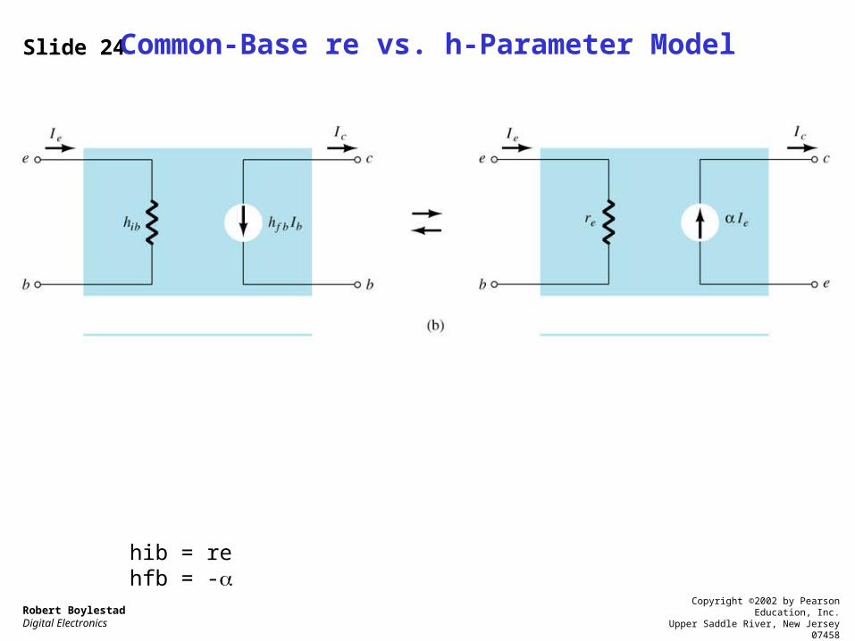
Common-Base re vs. h-Parameter Model
hib = rehfb = -
Slide 25
Robert BoylestadDigital Electronics
Copyright ©2002 by Pearson Education, Inc.Upper Saddle River, New Jersey 07458
All rights reserved.
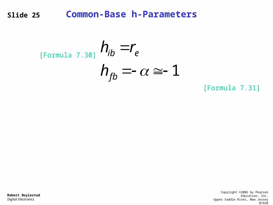
Common-Base h-Parameters
[Formula 7.30]
[Formula 7.31]
1
fb
eib
h
rh


![Various BJT Amplifiers (H.18)€¦ · Based [1] Floyd, Electronic Devices 7th ed [2] Cook, [2] en.wikipedia.org References Robert Boylestad & Louis Nashelsky Electronic Devices and](https://img.pdfslide.us/doc/110x75/5eaafe4ee4f4fa645422645b/various-bjt-ampliiers-h18-based-1-floyd-electronic-devices-7th-ed-2-cook.jpg)