Embed Size (px)
Citation preview
1
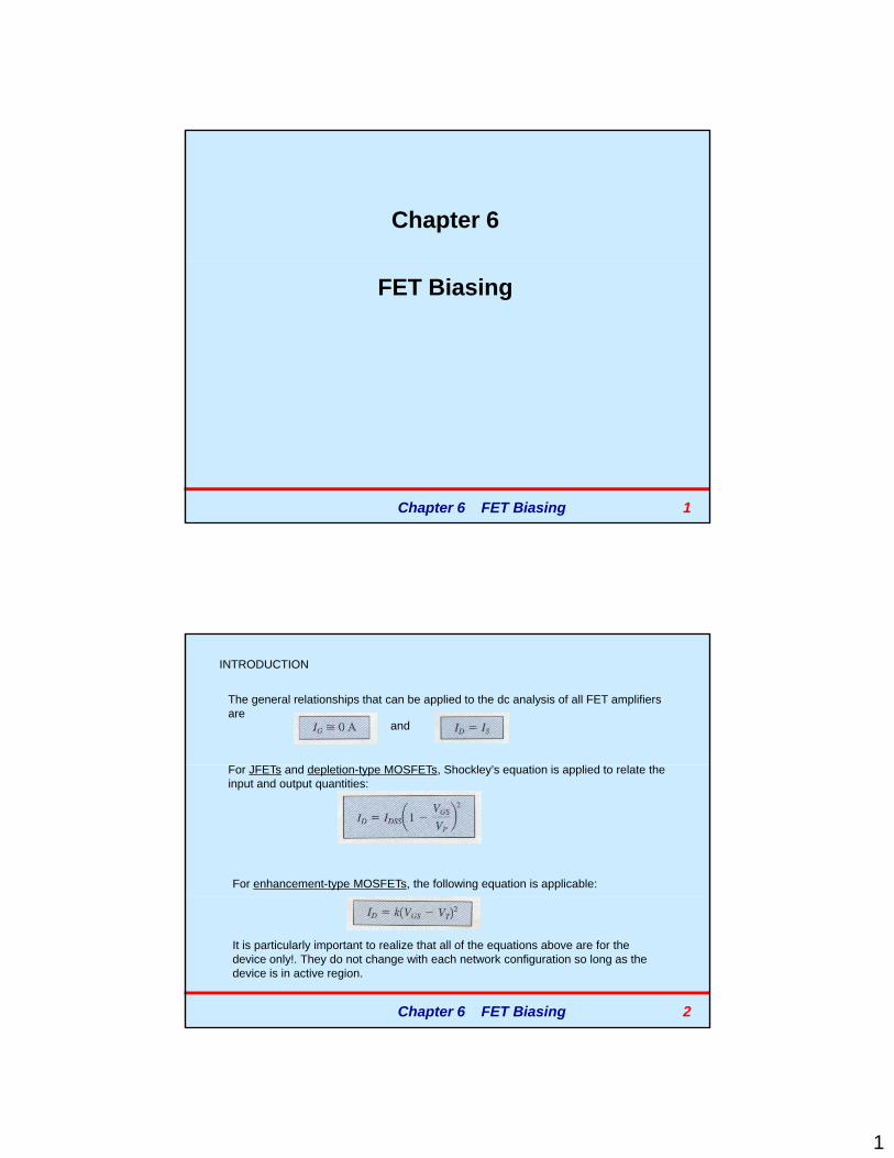
Chapter 6
FET Biasing
Chapter 6 FET Biasing 1
INTRODUCTION
The general relationships that can be applied to the dc analysis of all FET amplifiersare
and
For JFETs and depletion-type MOSFETs, Shockley’s equation is applied to relate theinput and output quantities:
For enhancement-type MOSFETs, the following equation is applicable:
It is particularly important to realize that all of the equations above are for the device only!. They do not change with each network configuration so long as the device is in active region.
Chapter 6 FET Biasing 2
2
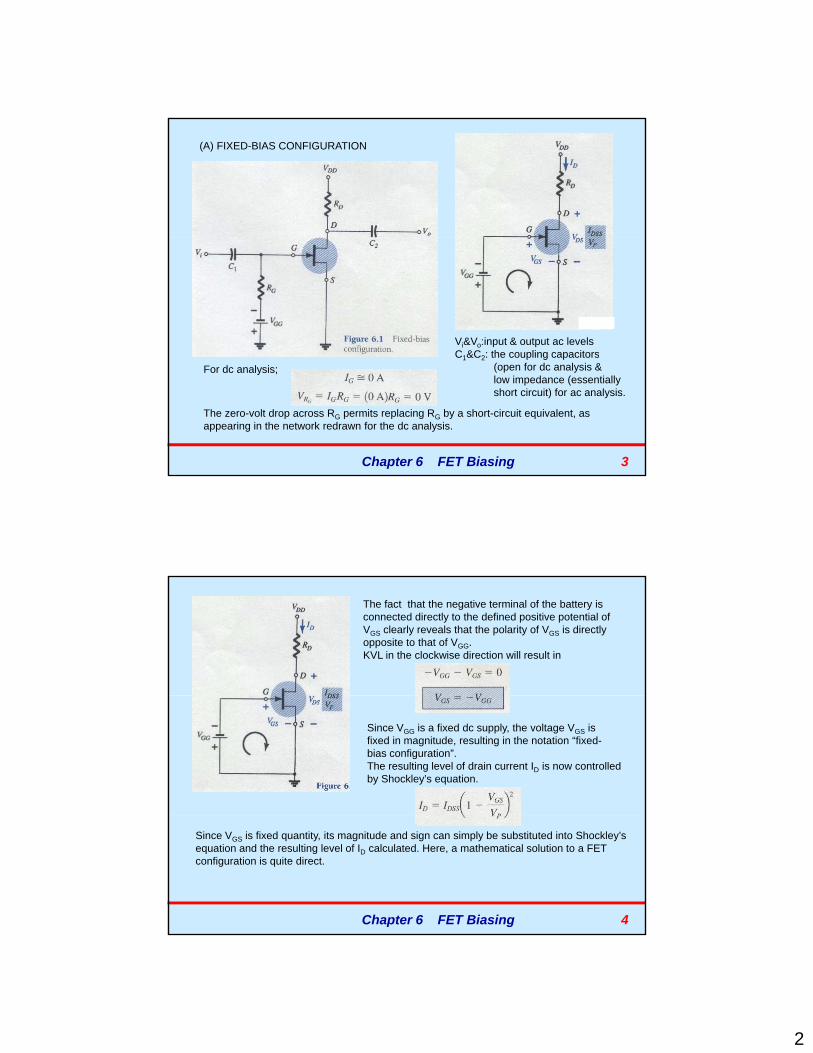
(A) FIXED-BIAS CONFIGURATION
Vi&Vo:input & output ac levelsC1&C2: the coupling capacitors
Chapter 6 FET Biasing 3
For dc analysis;
The zero-volt drop across RG permits replacing RG by a short-circuit equivalent, asappearing in the network redrawn for the dc analysis.
C1&C2: the coupling capacitors(open for dc analysis &low impedance (essentiallyshort circuit) for ac analysis.
The fact that the negative terminal of the battery isconnected directly to the defined positive potential ofVGS clearly reveals that the polarity of VGS is directlyopposite to that of VGG.KVL in the clockwise direction will result in
Since VGG is a fixed dc supply, the voltage VGS isfixed in magnitude, resulting in the notation “fixed-bias configuration”.The resulting level of drain current ID is now controlledby Shockley’s equation.
Chapter 6 FET Biasing 4
Since VGS is fixed quantity, its magnitude and sign can simply be substituted into Shockley’sequation and the resulting level of ID calculated. Here, a mathematical solution to a FETconfiguration is quite direct.
3
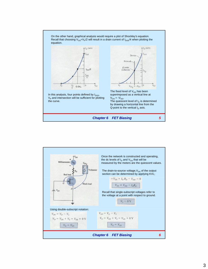
On the other hand, graphical analysis would require a plot of Shockley’s equation.Recall that choosing VGS=VP/2 will result in a drain current of IDSS/4 when plotting theequation.
IDSS/2
O.3VP
The fixed level of V has been
Chapter 6 FET Biasing 5
In this analysis, four points defined by IDSS,VP and intersection will be sufficient for plottingthe curve.
The fixed level of VGS has beensuperimposed as a vertical line at VGS = -VGG.The quiescent level of ID is determinedby drawing a horizontal line from theQ-point to the vertical ID axis.
Once the network is constructed and operating,the dc levels of ID and VGS that will be measured by the meters are the quiescent values.
The drain-to-source voltage,VDS of the outputsection can be determined by applying KVL;
Recall that single-subscript voltages refer tothe voltage at a point with respect to ground.
Chapter 6 FET Biasing 6
Using double-subscript notation:
4
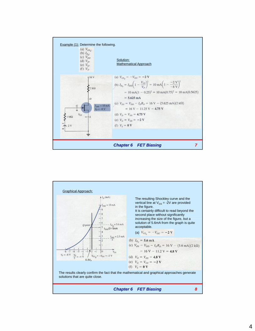
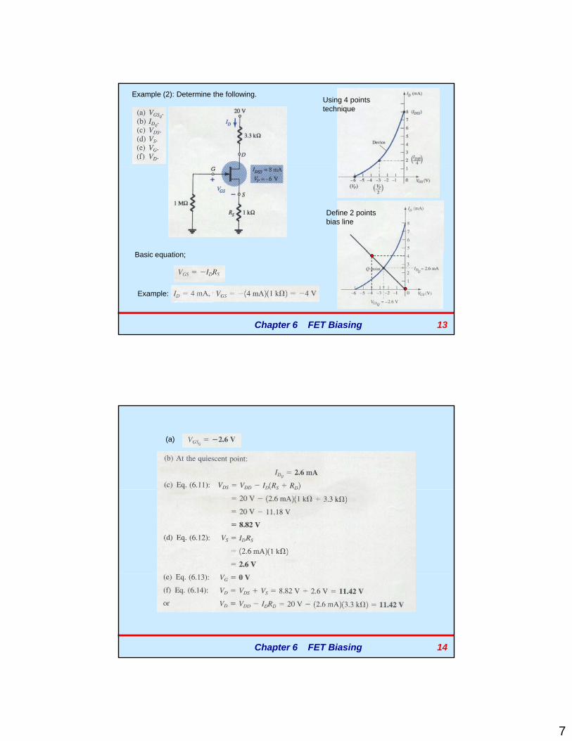
Example (1): Determine the following.
Solution:Mathematical Approach
Chapter 6 FET Biasing 7
Graphical Approach:
The resulting Shockley curve and thevertical line at VGS = -2V are providedin the figure.It is certainly difficult to read beyond thesecond place without significantlyincreasing the size of the figure but aincreasing the size of the figure, but asolution of 5.6mA from the graph is quiteacceptable.IDSS/2= 5mA
(a)
Chapter 6 FET Biasing 8
0.3VP
The results clearly confirm the fact that the mathematical and graphical approaches generatesolutions that are quite close.
5
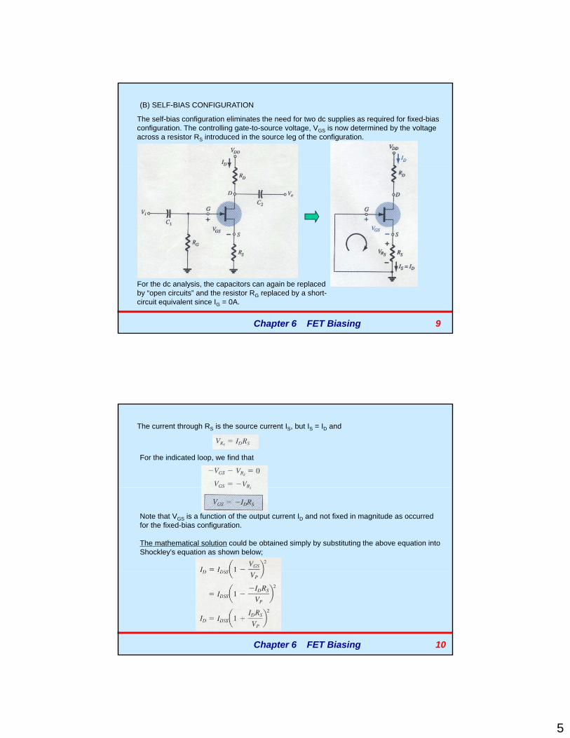
(B) SELF-BIAS CONFIGURATION
The self-bias configuration eliminates the need for two dc supplies as required for fixed-biasconfiguration. The controlling gate-to-source voltage, VGS is now determined by the voltageacross a resistor RS introduced in the source leg of the configuration.
Chapter 6 FET Biasing 9
For the dc analysis, the capacitors can again be replacedby “open circuits” and the resistor RG replaced by a short-circuit equivalent since IG = 0A.
The current through RS is the source current IS, but IS = ID and
For the indicated loop, we find that
Note that VGS is a function of the output current ID and not fixed in magnitude as occurredfor the fixed-bias configuration.
The mathematical solution could be obtained simply by substituting the above equation intoShockley’s equation as shown below;
Chapter 6 FET Biasing 10
6
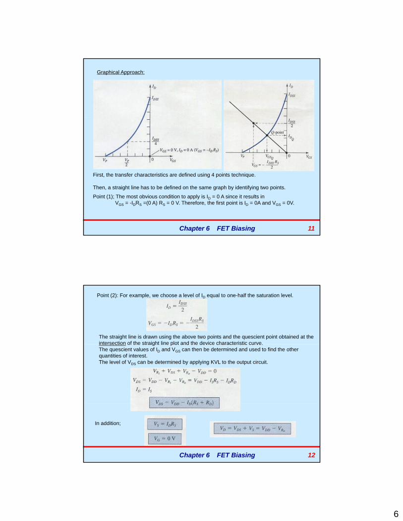
Graphical Approach:
First, the transfer characteristics are defined using 4 points technique.
Chapter 6 FET Biasing 11
st, t e t a s e c a acte st cs a e de ed us g po ts tec que
Then, a straight line has to be defined on the same graph by identifying two points.
Point (1); The most obvious condition to apply is ID = 0 A since it results inVGS = -IDRS =(0 A) RS = 0 V. Therefore, the first point is ID = 0A and VGS = 0V.
Point (2): For example, we choose a level of ID equal to one-half the saturation level.
The straight line is drawn using the above two points and the quescient point obtained at theintersection of the straight line plot and the device characteristic curveintersection of the straight line plot and the device characteristic curve.The quescient values of ID and VGS can then be determined and used to find the otherquantities of interest.The level of VDS can be determined by applying KVL to the output circuit.
Chapter 6 FET Biasing 12
In addition;
7
Example (2): Determine the following.Using 4 pointstechnique
Define 2 pointsbias line
Chapter 6 FET Biasing 13
Basic equation;
Example:
(a)
Chapter 6 FET Biasing 14
8
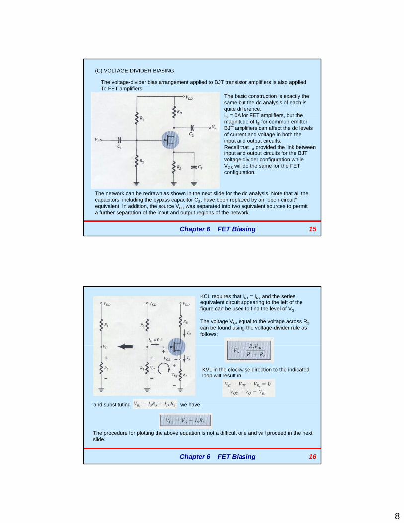
(C) VOLTAGE-DIVIDER BIASING
The voltage-divider bias arrangement applied to BJT transistor amplifiers is also appliedTo FET amplifiers.
The basic construction is exactly thesame but the dc analysis of each isquite difference.IG = 0A for FET amplifiers, but theG pmagnitude of IB for common-emitterBJT amplifiers can affect the dc levelsof current and voltage in both theinput and output circuits.Recall that IB provided the link betweeninput and output circuits for the BJTvoltage-divider configuration whileVGS will do the same for the FETconfiguration.
Chapter 6 FET Biasing 15
The network can be redrawn as shown in the next slide for the dc analysis. Note that all thecapacitors, including the bypass capacitor CS, have been replaced by an “open-circuit”equivalent. In addition, the source VDD was separated into two equivalent sources to permita further separation of the input and output regions of the network.
KCL requires that IR1 = IR2 and the seriesequivalent circuit appearing to the left of the figure can be used to find the level of VG.
The voltage VG, equal to the voltage across R2,can be found using the voltage-divider rule asfollows:
KVL in the clockwise direction to the indicatedloop will result in
and substituting we have
Chapter 6 FET Biasing 16
and substituting we have
The procedure for plotting the above equation is not a difficult one and will proceed in the nextslide.
9
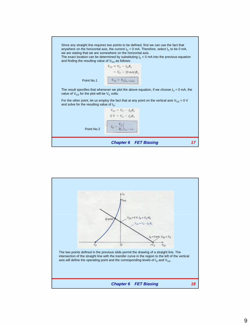
Since any straight line requires two points to be defined, first we can use the fact thatanywhere on the horizontal axis, the current ID = 0 mA. Therefore, select ID to be 0 mA,we are stating that we are somewhere on the horizontal axis.The exact location can be determined by substituting ID = 0 mA into the previous equationand finding the resulting value of VGS as follows:
The result specifies that whenever we plot the above equation, if we choose ID = 0 mA, thevalue of VGS for the plot will be VG volts.
Point No.1
For the other point, let us employ the fact that at any point on the vertical axis VGS = 0 Vand solve for the resulting value of ID:
Chapter 6 FET Biasing 17
Point No.2
The two points defined in the previous slide permit the drawing of a straight line The
Chapter 6 FET Biasing 18
The two points defined in the previous slide permit the drawing of a straight line. Theintersection of the straight line with the transfer curve in the region to the left of the verticalaxis will define the operating point and the corresponding levels of ID and VGS.
10
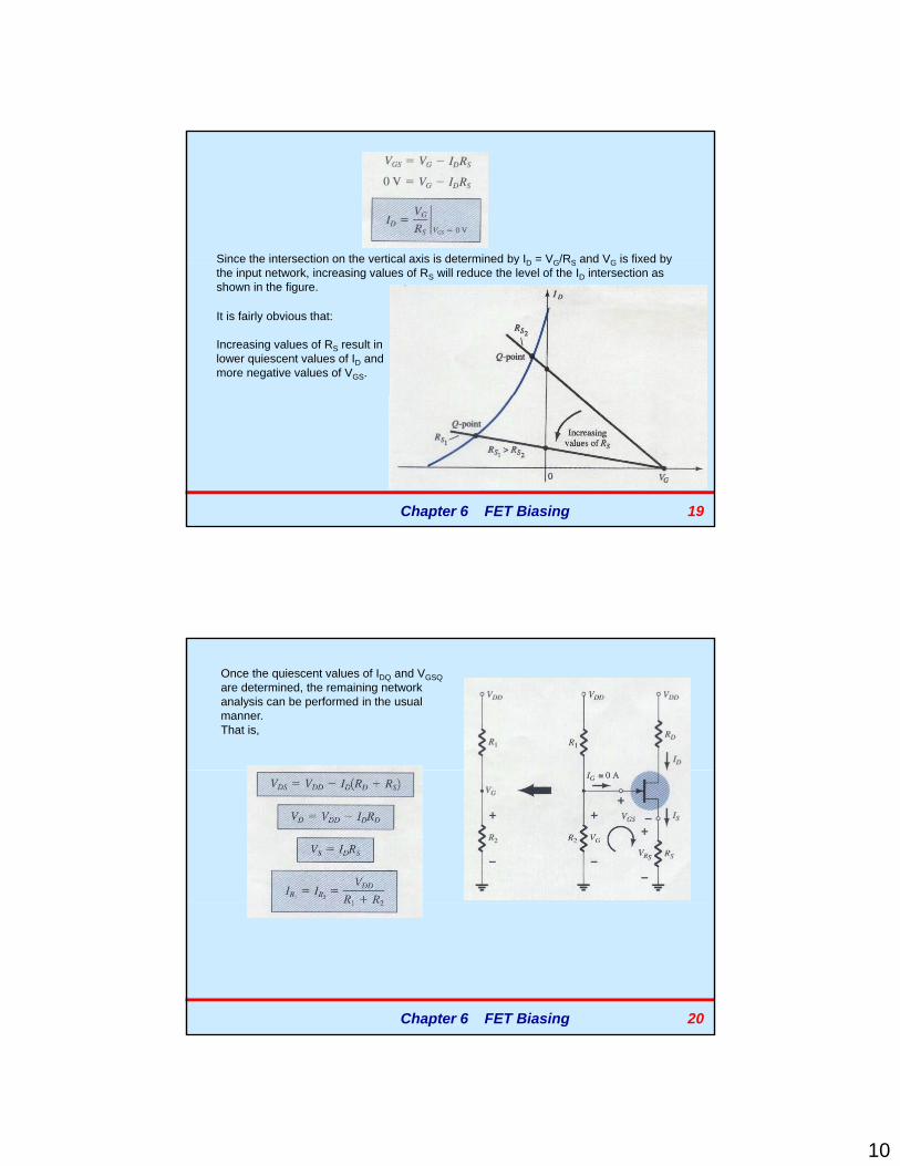
Since the intersection on the vertical axis is determined by ID = VG/RS and VG is fixed bySince the intersection on the vertical axis is determined by ID VG/RS and VG is fixed bythe input network, increasing values of RS will reduce the level of the ID intersection asshown in the figure.
It is fairly obvious that:
Increasing values of RS result inlower quiescent values of ID andmore negative values of VGS.
Chapter 6 FET Biasing 19
Once the quiescent values of IDQ and VGSQare determined, the remaining networkanalysis can be performed in the usualmanner.That is,
Chapter 6 FET Biasing 20
11
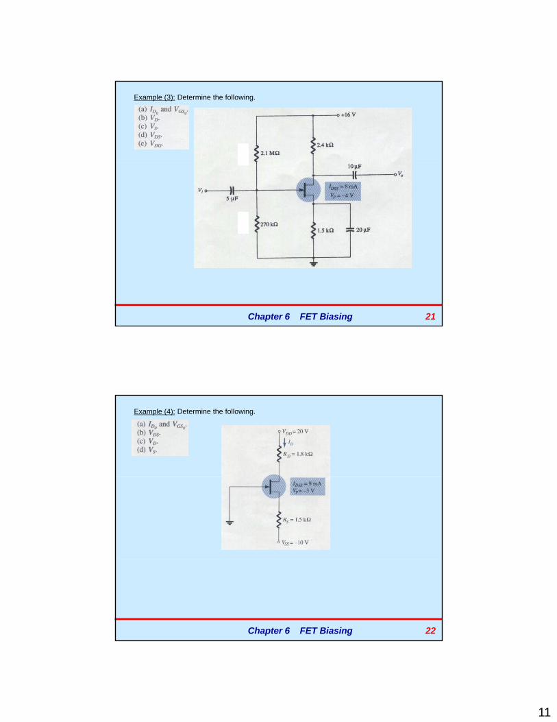
Example (3): Determine the following.
Chapter 6 FET Biasing 21
Example (4): Determine the following.
Chapter 6 FET Biasing 22
12
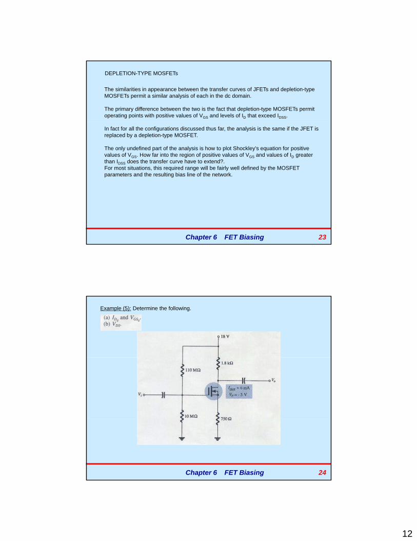
DEPLETION-TYPE MOSFETs
The similarities in appearance between the transfer curves of JFETs and depletion-typeMOSFETs permit a similar analysis of each in the dc domain.
The primary difference between the two is the fact that depletion-type MOSFETs permitoperating points with positive values of VGS and levels of ID that exceed IDSS.
In fact for all the configurations discussed thus far, the analysis is the same if the JFET isreplaced by a depletion-type MOSFET.
The only undefined part of the analysis is how to plot Shockley’s equation for positivevalues of VGS. How far into the region of positive values of VGS and values of ID greaterthan IDSS does the transfer curve have to extend?.For most situations, this required range will be fairly well defined by the MOSFETparameters and the resulting bias line of the network.
Chapter 6 FET Biasing 23
Example (5): Determine the following.
Chapter 6 FET Biasing 24
13
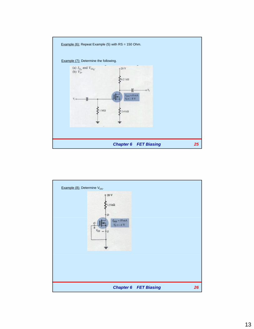
Example (6): Repeat Example (5) with RS = 150 Ohm.
Example (7): Determine the following.
Chapter 6 FET Biasing 25
Example (8): Determine VDS.
Chapter 6 FET Biasing 26
14
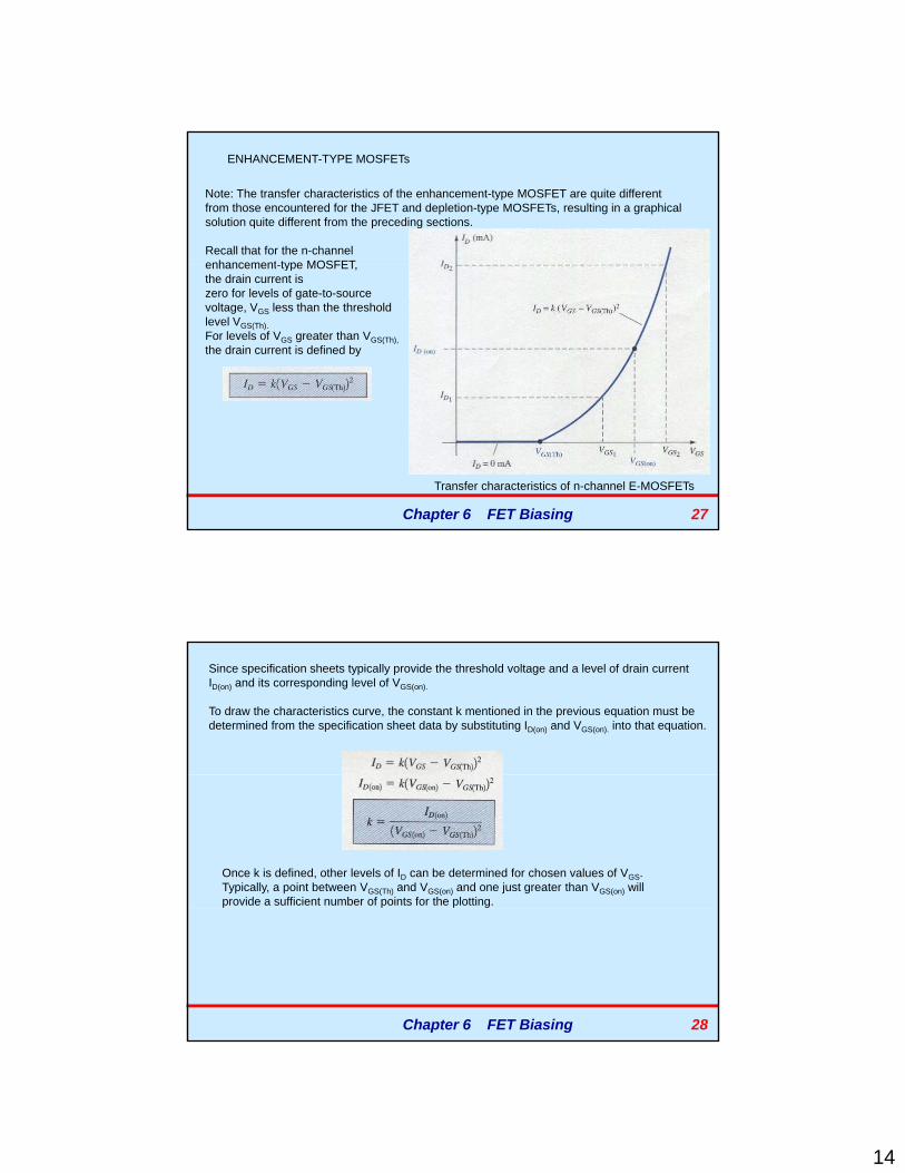
ENHANCEMENT-TYPE MOSFETs
Note: The transfer characteristics of the enhancement-type MOSFET are quite differentfrom those encountered for the JFET and depletion-type MOSFETs, resulting in a graphicalsolution quite different from the preceding sections.
Recall that for the n-channel enhancement type MOSFETenhancement-type MOSFET, the drain current is zero for levels of gate-to-source voltage, VGS less than the threshold level VGS(Th).For levels of VGS greater than VGS(Th),the drain current is defined by
Chapter 6 FET Biasing 27
Transfer characteristics of n-channel E-MOSFETs
Since specification sheets typically provide the threshold voltage and a level of drain currentID(on) and its corresponding level of VGS(on).
To draw the characteristics curve, the constant k mentioned in the previous equation must bedetermined from the specification sheet data by substituting ID(on) and VGS(on). into that equation.
Once k is defined, other levels of ID can be determined for chosen values of VGS.Typically, a point between VGS(Th) and VGS(on) and one just greater than VGS(on) willprovide a sufficient number of points for the plotting.
Chapter 6 FET Biasing 28
15
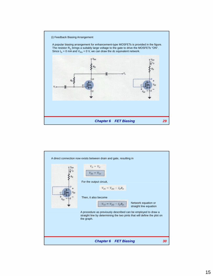
(i) Feedback Biasing Arrangement
A popular biasing arrangement for enhancement-type MOSFETs is provided in the figure.The resistor RG brings a suitably large voltage to the gate to drive the MOSFETs “ON”.Since IG = 0 mA and VRG = 0 V, we can draw the dc equivalent network.
Chapter 6 FET Biasing 29
A direct connection now exists between drain and gate, resulting in
For the output circuitFor the output circuit,
Then, it also become
A procedure as previously described can be employed to draw a
Network equation or straight line equation
Chapter 6 FET Biasing 30
straight line by determining the two pints that will define the plot onthe graph.
16
Substituting ID = 0 mA;
Substituting VGS = 0 V;
Chapter 6 FET Biasing 31
Example (9): Determine IDQ and VGSQ.
Chapter 6 FET Biasing 32
17
(ii) Voltage-Divider Biasing Arrangement
A second popular biasing arrangement for the enhancement-type MOSFETs.
The fact that IG = 0 mA results in the following equation for VGGas derived from the application of the voltage-divider rule.
Applying KVL around the indicated loop will result in
Chapter 6 FET Biasing 33
For the output section;Once IDQ and VGSQ are known, all the remainingquantities such as VDS,VD and VS can be determined.
Example (10): Determine IDQ , VGSQ.and VDS.
Chapter 6 FET Biasing 34