Embed Size (px)
Citation preview

Chapter 5: Verilog (Part 1)Based on the material presented in Chap. 4, there are a few observations about logic design that are
apparent. First, the size of logic circuitry can scale quickly to the point where it is difficult to design byhand. Second, the process of moving from a high-level description of how a circuit works (e.g., a truthtable) to a form that is ready to be implemented with real circuitry (e.g., a minimized logic diagram) isstraightforward and well-defined. Both of these observations motivate the use of computer aided design(CAD) tools to accomplish logic design. This chapter introduces hardware description languages (HDLs)as a means to describe digital circuitry using a text-based language. HDLs provide a means to describelarge digital systems without the need for schematics, which can become impractical in very largedesigns. HDLs have evolved to support logic simulation at different levels of abstraction. This providesdesigners the ability to begin designing and verifying functionality of large systems at a high level ofabstraction and postpone the details of the circuit implementation until later in the design cycle. Thisenables a top-down design approach that is scalable across different logic families. HDLs have alsoevolved to support automated synthesis, which allows the CAD tools to take a functional description of asystem (e.g., a truth table) and automatically create the gate level circuitry to be implemented in realhardware. This allows designers to focus their attention on designing the behavior of a system and notspend as much time performing the formal logic synthesis steps that were presented in Chap. 4. Theintent of this chapter is to introduce HDLs and their use in the modern digital design flow. This chapter willcover the basics of designing combinational logic in an HDL and also hierarchical design. The moreadvanced concepts of HDLs such as sequential logic design, high level abstraction, and test benchesare covered later so that the reader can get started quickly using HDLs to gain experience with thelanguages and design flow.
There are two dominant hardware description languages in use today. They are VHDL and Verilog.VHDL stands for very high speed integrated circuit hardware description language. Verilog is not anacronym but rather a trade name. The use of these two HDLs is split nearly equally within the digitaldesign industry. Once one language is learned it is simple to learn the other language, so the choice ofthe HDL to learn first is somewhat arbitrary. In this text, we will use Verilog to learn the concepts of anHDL. Verilog is more similar to the programming language C and less strict in its type casting than VHDL.Verilog is also widely used in custom integrated circuit design so there is a great deal of documentationand examples readily available online. The goal of this chapter is to provide an understanding of thebasic principles of hardware description languages.
Learning Outcomes—After completing this chapter, you will be able to:
5.1 Describe the role of hardware description languages in modern digital design.5.2 Describe the fundamentals of design abstraction in modern digital design.5.3 Describe the modern digital design flow based on hardware description languages.5.4 Describe the fundamental constructs of Verilog.5.5 Design a Verilog model for a combinational logic circuit using concurrent modeling
techniques (continuous signal assignment with logical operators and continuous signalassignment with conditional operators).
5.6 Design a Verilog model for a combinational logic circuit using a structural design approach(gate level primitives and user defined primitives).
5.7 Describe the role of a Verilog test bench.
# Springer International Publishing AG 2017B.J. LaMeres, Introduction to Logic Circuits & Logic Design with Verilog,DOI 10.1007/978-3-319-53883-9_5
141

5.1 History of Hardware Description Languages
The invention of the integrated circuit is most commonly credited to two individuals who filed patentson different variations of the same basic concept within six months of each other in 1959. Jack Kilby filedthe first patent on the integrated circuit in February of 1959 titled “Miniaturized Electronic Circuits” whileworking for Texas Instruments. Robert Noyce was the second to file a patent on the integrated circuit inJuly of 1959 titled “Semiconductor Device and Lead Structure” while at a company he cofounded calledFairchild Semiconductor. Kilby went on to win the Nobel Prize in Physics in 2000 for his invention, whileNoyce went on to cofound Intel Corporation in 1968 with Gordon Moore. In 1971, Intel introduced the firstsingle-chip microprocessor using integrated circuit technology, the Intel 4004. This microprocessor ICcontained 2300 transistors. This series of inventions launched the semiconductor industry, which wasthe driving force behind the growth of Silicon Valley, and led to 40 years of unprecedented advancementin technology that has impacted every aspect of the modern world.
Gordon Moore, cofounder of Intel, predicted in 1965 that the number of transistors on an integratedcircuit would double every two years. This prediction, now known asMoore’s Law, has held true since theinvention of the integrated circuit. As the number of transistors on an integrated circuit grew, so did thesize of the design and the functionality that could be implemented. Once the first microprocessor wasinvented in 1971, the capability of CAD tools increased rapidly enabling larger designs to be accom-plished. These larger designs, including newer microprocessors, enabled the CAD tools to become evenmore sophisticated and, in turn, yield even larger designs. The rapid expansion of electronic systemsbased on digital integrated circuits required that different manufacturers needed to produce designs thatwere compatible with each other. The adoption of logic family standards helped manufacturers ensuretheir parts would be compatible with other manufacturers at the physical layer (e.g., voltage and current);however, one challenge that was encountered by the industry was a way to document the complexbehavior of larger systems. The use of schematics to document large digital designs became toocumbersome and difficult to understand by anyone besides the designer. Word descriptions of thebehavior were easier to understand, but even this form of documentation became too voluminous tobe effective for the size of designs that were emerging. Simultaneously there was a need to beginsimulating the functionality of these large systems prior to fabrication to verify accuracy. Due to thecomplexity of these systems and the vast potential for design error, it became impractical to verify designaccuracy through prototyping.
In 1983, the US Department of Defense (DoD) sponsored a program to create a means to documentthe behavior of digital systems that could be used across all of its suppliers. This program was motivatedby a lack of adequate documentation for the functionality of application specific integrated circuits(ASICs) that were being supplied to the DoD. This lack of documentation was becoming a criticalissue as ASICs would come to the end of their life cycle and need to be replaced. With the lack of astandardized documentation approach, suppliers had difficulty reproducing equivalent parts to those thathad become obsolete. The DoD contracted three companies (Texas Instruments, IBM, and Intermetrics)to develop a standardized documentation tool that provided detailed information about both the interface(i.e., inputs and outputs) and the behavior of digital systems. The new tool was to be implemented in aformat similar to a programming language. Due to the nature of this type of language-based tool, it was anatural extension of the original project scope to include the ability to simulate the behavior of a digitalsystem. The simulation capability was desired to span multiple levels of abstraction to provide maximumflexibility. In 1985, the first version of this tool, called VHDL, was released. In order to gain widespreadadoption and ensure consistency of use across the industry, VHDL was turned over to the Institute ofElectrical and Electronic Engineers (IEEE) for standardization. IEEE is a professional association thatdefines a broad range of open technology standards. In 1987, IEEE released the first industry standardversion of VHDL. The release was titled IEEE 1076–1987. Feedback from the initial version resulted in amajor revision of the standard in 1993 titled IEEE 1076–1993. While many minor revisions have been
142 • Chapter 5: Verilog (Part 1)

made to the 1993 release, the 1076–1993 standard contains the vast majority of VHDL functionality inuse today. The most recent VHDL standard is IEEE 1076–2008.
Also in 1983, the Verilog HDL was developed by Automated Integrated Design Systems as a logicsimulation language. The development of Verilog took place completely independent from the VHDLproject. Automated Integrated Design Systems (renamed Gateway Design Automation in 1985) wasacquired by CAD tool vendorCadence Design Systems in 1990. In response to the popularity of Verilog’sintuitive programming and superior simulation support, and also to stay competitive with the emergingVHDL standard, Cadence made the Verilog HDL open to the public. IEEE once again developed theopen standard for this HDL, and in 1995 released the Verilog standard titled IEEE 1364–1995. Thisrelease has undergone numerous revisions with the most significant occurring in 2001. It is common torefer to the major releases as “Verilog 1995” and “Verilog 2001” instead of their official standard numbers.
The development of CAD tools to accomplish automated logic synthesis can be dated back to the1970’s when IBM began developing a series of practical synthesis engines that were used in the designof their mainframe computers; however, the main advancement in logic synthesis came with the foundingof a company called Synopsis in 1986. Synopsis was the first company to focus on logic synthesisdirectly from HDLs. This was a major contribution because designers were already using HDLs todescribe and simulate their digital systems, and now logic synthesis became integrated in the samedesign flow. Due to the complexity of synthesizing highly abstract functional descriptions, only lower-levels of abstraction that were thoroughly elaborated were initially able to be synthesized. As CAD toolcapability evolved, synthesis of higher levels of abstraction became possible, but even today not allfunctionality that can be described in an HDL can be synthesized.
The history of HDLs, their standardization, and the creation of the associated logic synthesis tools iskey to understanding the use and limitations of HDLs. HDLs were originally designed for documentationand behavioral simulation. Logic synthesis tools were developed independently and modified later towork with HDLs. This history provides some background into the most common pitfalls that beginningdigital designers encounter, that being that most any type of behavior can be described and simulated inan HDL, but only a subset of well-described functionality can be synthesized. Beginning digital designersare often plagued by issues related to designs that simulate perfectly but that will not synthesizecorrectly. In this book, an effort is made to introduce Verilog at a level that provides a reasonable amountof abstraction while preserving the ability to be synthesized. Figure 5.1 shows a timeline of some of themajor technology milestones that have occurred in the past 150 years in the field of digital logic andHDLs.
5.1 History of Hardware Description Languages • 143

CONCEPT CHECK
CC5.1 Why does Verilog support modeling techniques that aren’t synthesizable?
(A) There wasn’t enough funding available to develop synthesis capability as it all wentto the VHDL project.
(B) At the time Verilog was created, synthesis was deemed too difficult to implement.
(C) To allow Verilog to be used as a generic programming language.
(D) Verilog needs to support all steps in the modern digital design flow, some of whichare unsynthesizable such as test pattern generation and timing verification.
Fig. 5.1Major milestones in the advancement of Digital Logic and HDLs
144 • Chapter 5: Verilog (Part 1)

5.2 HDL Abstraction
HDLs were originally defined to be able to model behavior at multiple levels of abstraction.Abstraction is an important concept in engineering design because it allows us to specify how systemswill operate without getting consumed prematurely with implementation details. Also, by removing thedetails of the lower level implementation, simulations can be conducted in reasonable amounts of time tomodel the higher-level functionality. If a full computer system was simulated using detailed models forevery MOSFET, it would take an impracticable amount of time to complete. Figure 5.2 shows a graphicaldepiction of the different layers of abstraction in digital system design.
The highest level of abstraction is the system level. At this level, behavior of a system is describedby stating a set of broad specifications. An example of a design at this level is a specification such as “thecomputer system will perform 10 Tera Floating Point Operations per Second (10 TFLOPS) on double
Fig. 5.2Levels of design abstraction
5.2 HDL Abstraction • 145

precision data and consume no more than 100 Watts of power”. Notice that these specifications do notdictate the lower level details such as the type of logic family or the type of computer architecture to use.One level down from the system level is the algorithmic level. At this level, the specifications begin to bebroken down into sub-systems, each with an associated behavior that will accomplish a part of theprimary task. At this level, the example computer specifications might be broken down into sub-systemssuch as a central processing unit (CPU) to perform the computation and random access memory (RAM)to hold the inputs and outputs of the computation. One level down from the algorithmic level is theregister transfer level (RTL). At this level, the details of how data is moved between and withinsub-systems are described in addition to how the data is manipulated based on system inputs. Onelevel down from the RTL level is the gate level. At this level, the design is described using basic gates andregisters (or storage elements). The gate level is essentially a schematic (either graphically or text-based) that contains the components and connections that will implement the functionality from theabove levels of abstraction. One level down from the gate level is the circuit level. The circuit leveldescribes the operation of the basic gates and registers using transistors, wires and other electricalcomponents such as resistors and capacitors. Finally, the lowest level of design abstraction is thematerial level. This level describes how different materials are combined and shaped in order toimplement the transistors, devices and wires from the circuit level.
HDLs are designed to model behavior at all of these levels with the exception of the material level.While there is some capability to model circuit level behavior such as MOSFETs as ideal switches andpull-up/pull-down resistors, HDLs are not typically used at the circuit level. Another graphical depiction ofdesign abstraction is known as the Gajski and Kuhn’s Y-chart. A Y-chart depicts abstraction acrossthree different design domains: behavioral, structural and physical. Each of these design domainscontains levels of abstraction (i.e., system, algorithm, RTL, gate, and circuit). An example Y-chart isshown in Fig. 5.3.
146 • Chapter 5: Verilog (Part 1)

A Y-chart also depicts how the abstraction levels of different design domains are related to eachother. A top-down design flow can be visualized in a Y-chart by spiraling inward in a clockwise direction.Moving from the behavioral domain to the structural domain is the process of synthesis. Wheneversynthesis is performed, the resulting system should be compared with the prior behavioral description.This checking is called verification. The process of creating the physical circuitry corresponding to thestructural description is called implementation. The spiral continues down through the levels of abstrac-tion until the design is implemented at a level that the geometries representing circuit elements(transistors, wires, etc.) are ready to be fabricated in silicon. Figure 5.4 shows the top-down designprocess depicted as an inward spiral on the Y-chart.
Fig. 5.3Y-Chart of design abstraction
5.2 HDL Abstraction • 147

The Y-chart represents a formal approach for large digital systems. For large systems that aredesigned by teams of engineers, it is critical that a formal, top-down design process is followed toeliminate potentially costly design errors as the implementation is carried out at lower levels ofabstraction.
CONCEPT CHECK
CC5.2 Why is abstraction an essential part of engineering design?
(A) Without abstraction all schematics would be drawn at the transistor-level.
(B) Abstraction allows computer programs to aid in the design process.
(C) Abstraction allows the details of the implementation to be hidden while the higher-level systems are designed. Without abstraction, the details of the implementationwould overwhelm the designer.
(D) Abstraction allows analog circuit designers to include digital blocks in their systems.
Fig. 5.4Y-Chart illustrating top-down design approach
148 • Chapter 5: Verilog (Part 1)

5.3 The Modern Digital Design Flow
When performing a smaller design or the design of fully-contained sub-systems, the process can bebroken down into individual steps. These steps are shown in Fig. 5.5. This process is given genericallyand applies to both classical andmodern digital design. The distinction between classical and modern isthat modern digital design uses HDLs and automated CAD tools for simulation, synthesis, place androute, and verification.
This generic design process flow can be used across classical and modern digital design, althoughmodern digital design allows additional verification at each step using automated CAD tools. Figure 5.6shows how this flow is used in the classical design approach of a combinational logic circuit.
Fig. 5.5Generic digital design flow
5.3 The Modern Digital Design Flow • 149

The modern design flow based on HDLs includes the ability to simulate functionality at each step ofthe process. Functional simulations can be performed on the initial behavioral description of the system.At each step of the design process the functionality is described in more detail, ultimately moving towardthe fabrication step. At each level, the detailed information can be included in the simulation to verify thatthe functionality is still correct and that the design is still meeting the original specifications. Figure 5.7shows the modern digital design flow with the inclusion of simulation capability at each step.
Fig. 5.6Classical digital design flow
150 • Chapter 5: Verilog (Part 1)

CONCEPT CHECK
CC5.3 Why did digital designs move from schematic-entry to text-based HDLs?
(A) HDL models could be much larger by describing functionality in text similar totraditional programming language.
(B) Schematics required sophisticated graphics hardware to display correctly.
(C) Schematics symbols became too small as designs became larger.
(D) Text was easier to understand by a broader range of engineers.
Fig. 5.7Modern digital design flow
5.3 The Modern Digital Design Flow • 151

5.4 Verilog Constructs
Now we begin looking at the details of Verilog. The original Verilog standard (IEEE 1364) has beenupdated numerous times since its creation in 1995. The most significant update occurred in 2001, whichwas titled IEEE 1394–2001. In 2005 minor corrections and improvements were added to the standard,which resulted in IEEE 1394–2005. The constructs described in this book reflect the functionality in theIEEE 1394–2005 standard. The functionality of Verilog (e.g., operators, signal types, functions, etc.) isdefined within the Verilog standard, thus it is not necessary to explicitly state that a design is using theIEEE 1394 package because it is inherent in the use of Verilog. This chapter gives an overview of thebasic constructs of Verilog in order to model simple combinational logic circuits and begin gainingexperience with logic simulations. The more advanced constructs of Verilog are covered in Chap. 8with examples given throughout Chaps. 9, 10, 11, 12, and 13.
A Verilog design describes a single system in a single file. The file has the suffix *.v. Within the file,the system description is contained within a module. The module includes the interface to the system(i.e., the inputs and outputs) and the description of the behavior. Figure 5.8 shows a graphical depictionof a Verilog file.
Verilog is case sensitive. Also, each Verilog assignment, definition or declaration is terminated witha semicolon (;). As such, line wraps are allowed and do not signify the end of an assignment, definition ordeclaration. Line wraps can be used to make Verilog more readable. Comments in Verilog are supportedin two ways. The first way is called a line comment and is preceded with two slashes (i.e., //). Everythingafter the slashes is considered a comment until the end of the line. The second comment approach iscalled a block comment and begins with /* and ends with a */. Everything between /* and */ is considereda comment. A block comment can span multiple lines. All user-defined names in Verilog must start withan alphabetic letter, not a number. User-defined names are not allowed to be the same as any Verilogkeyword. This chapter contains many definitions of syntax in Verilog. The following notations will be usedthroughout the chapter when introducing new constructs.
bold ¼ Verilog keyword, use as is, case sensitive.
italics ¼ User-defined name, case sensitive.
<> ¼ A required characteristic such as a data type, input/output, etc.
Fig. 5.8The anatomy of a Verilog file
152 • Chapter 5: Verilog (Part 1)

5.4.1 Data Types
In Verilog, every signal, constant, variable and function must be assigned a data type. The IEEE1394–2005 standard provides a variety of pre-defined data types. Some data types are synthesizable,while others are only for modeling abstract behavior. The following are the most commonly used datatypes in the Verilog language.
5.4.1.1 Value Set
Verilog supports four basic values that a signal can take on: 0, 1, X, and Z. Most of the pre-defineddata types in Verilog store these values. A description of each value supported is given below.
Value Description
0 A logic zero, or false condition.
1 A logic one, or true condition.
x or X Unknown or uninitialized.
z or Z High impedance, tri-stated, or floating.
In Verilog, these values also have an associated strength. The strengths are used to resolve thevalue of a signal when it is driven by multiple sources. The names, syntax and relative strengths aregiven below.
Strength Description Strength level
supply1 Supply drive for VCC 7
supply0 Supply drive for VSS, or GND 7
strong1 Strong drive to logic one 6
strong0 Strong drive to logic zero 6
pull1 Medium drive to logic one 5
pull0 Medium drive to logic zero 5
large Large capacitive 4
weak1 Weak drive to logic one 3
weak0 Weak drive to logic zero 3
medium Medium capacitive 2
small Small capacitive 1
highz1 High impedance with weak pull-up to logic one 0
highz0 High impedance with weak pull-down to logic zero 0
When a signal is driven by multiple drivers, it will take on the value of the driver with the higheststrength. If the two drivers have the same strength, the value will be unknown. If the strength is notspecified, it will default to strong drive, or level 6.
5.4.1.2 Net Data Types
Every signal within Verilog must be associated with a data type. A net data type is one that modelsan interconnection (aka., a net) between components and can take on the values 0, 1, X, and Z. A signalwith a net data type must be driven at all times and updates its value when the driver value changes. Themost common synthesizable net data type in Verilog is the wire. The type wire will be used throughoutthis text. There are also a variety of other more advanced net data types that model complex digitalsystems with multiple drivers for the same net. The syntax and description for all Verilog net data typesare given below.
5.4 Verilog Constructs • 153

Type Description
wire A simple connection between components.
wor Wired-OR. If multiple drivers, their values are OR’d together.
wand Wired-AND’d. If multiple drivers, their values are AND’d together.
supply0 Used to model the VSS, (GND), power supply (supply strength inherent).
supply1 Used to model the VCC power supply (supply strength inherent).
tri Identical to wire. Used for readability for a net driven by multiple sources.
trior Identical to wor. Used for readability for nets driven by multiple sources.
triand Identical to wand. Used for readability for nets driven by multiple sources.
tri1 Pulls up to logic one when tri-stated.
tri0 Pulls down to logic zero when tri-stated.
trireg Holds last value when tri-stated (capacitance strength inherent).
Each of these net types can also have an associated drive strength. The strength is used indetermining the final value of the net when it is connected to multiple drivers.
5.4.1.3 Variable Data Types
Verilog also contains data types that model storage. These are called variable data types. A variabledata type can take on the values 0, 1, X, and Z, but does not have an associated strength. Variable datatypes will hold the value assigned to them until their next assignment. The syntax and description for theVerilog variable data types are given below.
Type Description
reg A variable that models logic storage. Can take on values 0, 1, X, and Z.
integer A 32-bit, 2’s complement variable representing whole numbers between�2,147,483,64810 to +2,147,483,647.
real A 64-bit, floating point variable representing real numbers between –(2.2x10�308)10to +(2.2x10308)10.
time An unsigned, 64-bit variable taking on values from 010 to +(9.2x10¹⁸).
realtime Same as time. Just used for readability.
5.4.1.4 Vectors
In Verilog, a vector is a one-dimensional array of elements. All of the net data types, in addition to thevariable type reg, can be used to form vectors. The syntax for defining a vector is as follows:
<type> [<MSB_index>:<LSB_index>] vector_name
While any range of indices can be used, it is common practice to have the LSB index start at zero.
Example:
wire [7:0] Sum; // This defines an 8-bit vector called “Sum” of type wire. The// MSB is given the index 7 while the LSB is given the index 0.
reg [15:0] Q; // This defines a 16-bit vector called “Q” of type reg.
Individual bits within the vector can be addressed using their index. Groups of bits can be accessedusing an index range.
Sum[0]; // This is the least significant bit of the vector “Sum” definedabove.
Q[15:8]; // This is the upper 8-bits of the 16-bit vector “Q” definedabove.
154 • Chapter 5: Verilog (Part 1)

5.4.1.5 Arrays
An array is a multi-dimensional array of elements. This can also be thought of as a “vector ofvectors”. Vectors within the array all have the same dimensions. To declare an array, the element typeand dimensions are defined first followed by the array name and its dimensions. It is common practice toplace the start index of the array on the left side of the “:”when defining its dimensions. The syntax for thecreation of an array is shown below.
<element_type> [<MSB_index>:<LSB_index>] array_name [<array_start_index>:<array_end_index>];
Example:
reg[7:0] Mem[0:4095]; // Defines an array of 4096, 8-bit vectors of type reg.integer A[1:100]; // Defines an array of 100 integers.
When accessing an array, the name of the array is given first, followed by the index of the element. Itis also possible to access an individual bit within an array by adding appending the index of element.
Example:
Mem[2]; // This is the 3rd element within the array named “Mem”.// This syntax represents an 8-bit vector of type reg.
Mem[2][7]; // This is the MSB of the 3rd element within the array named “Mem”.// This syntax represents a single bit of type reg.
A[2]; // This is the 2nd element within the array named “A”. Recall// that A was declared with a starting index of 1.// This syntax represents a 32-bit, signed integer.
5.4.1.6 Expressing Numbers Using Different Bases
If a number is simply entered into Verilog without identifying syntax, it is treated as an integer.However, Verilog supports defining numbers in other bases. Verilog also supports an optional bit sizeand sign of a number. When defining the value of arrays, the “_” can be inserted between numerals toimprove readability. The “_” is ignored by the Verilog compiler. Values of numbers can be entered ineither upper or lower case (i.e., z or Z, f or F, etc.). The syntax for specifying the base of a number is asfollows:
<size_in_bits>’<base><value>
Note that specifying the size is optional. If it is omitted, the number will default to a 32-bit vector withleading zeros added as necessary. The supported bases are as follows:
Syntax Description
‘b Unsigned binary
‘o Unsigned octal
‘d Unsigned decimal
‘h Unsigned hexadecimal
‘sb Signed binary
‘so Signed octal
‘sd Signed decimal
‘sh Signed hexadecimal
5.4 Verilog Constructs • 155

Example:
10 // This is treated as decimal 10, which is a 32-bit signed vector.4’b1111 // A 4-bit number with the value 11112.8’b1011_0000 // An 8-bit number with the value 101100002.8’hFF // An 8-bit number with the value 111111112.8’hff // An 8-bit number with the value 111111112.6’hA // A 6-bit number with the value 0010102. Note that leading zeros
// were added to make the value 6-bits.8’d7 // An 8-bit number with the value 000001112.32’d0 // A 32-bit number with the value 0000_000016.’b1111 // A 32-bit number with the value 0000_000F16.8’bZ // An 8-bit number with the value ZZZZ_ZZZZ.
5.4.1.7 Assigning Between Different Types
Verilog is said to be a weakly-typed (or loosely typed) language, meaning that it permitsassignments between different data types. This is as opposed to a strongly-typed language (such asVHDL) where signal assignments are only permitted between like types. The reason Verilog permitsassignment between different types is because it treats all of its types as just groups of bits. Whenassigning between different types, Verilog will automatically truncate or add leading bits as necessary tomake the assignment work. The following examples illustrate how Verilog handles a few assignmentsbetween different types. Assume that a variable called ABC_TB has been declared as type reg[2:0].
Example:
ABC_TB ¼ 2’b00; // ABC_TB will be assigned 3’b000. A leading bit is automaticallyadded.
ABC_TB ¼ 5; // ABC_TB will be assigned 3’b101. The integer is truncated to3-bits.
ABC_TB ¼ 8; // ABC_TB will be assigned 3’b000. The integer is truncated to3-bits.
5.4.2 The Module
All systems in Verilog are encapsulated inside of a module. Modules can include instantiations oflower-level modules in order to support hierarchical designs. The keywords module and endmodulesignify the beginning and end of the system description. When working on large designs, it is commonpractice to place each module in its own file with the same name.
module module_name (port_list); // Pre Verilog-2001// port_definitions// module_items
endmodule
or
module module_name (port_list and port_definitions); // Verilog-2001 and after// module_items
endmodule
5.4.2.1 Port Definitions
The first item within a module is its definition of the inputs and outputs, or ports. Each port needs tohave a user-defined name, a direction, and a type. The user-defined port names are case sensitive andmust begin an alphabetic character. The port directions are declared to be one of the three types: input,output, and inout. A port can take on any of the previously described data types, but only wires,
156 • Chapter 5: Verilog (Part 1)
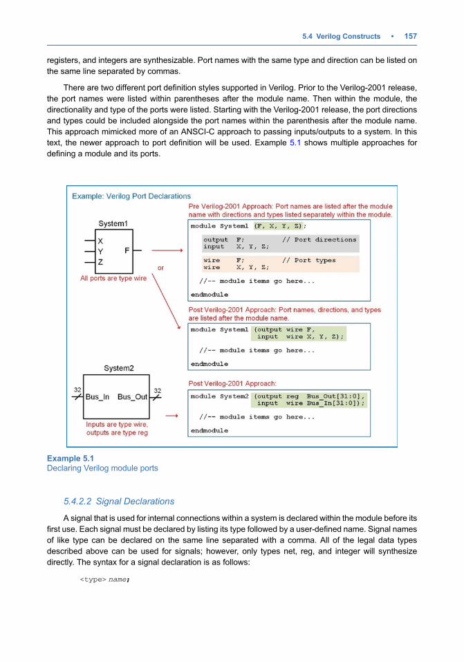
registers, and integers are synthesizable. Port names with the same type and direction can be listed onthe same line separated by commas.
There are two different port definition styles supported in Verilog. Prior to the Verilog-2001 release,the port names were listed within parentheses after the module name. Then within the module, thedirectionality and type of the ports were listed. Starting with the Verilog-2001 release, the port directionsand types could be included alongside the port names within the parenthesis after the module name.This approach mimicked more of an ANSCI-C approach to passing inputs/outputs to a system. In thistext, the newer approach to port definition will be used. Example 5.1 shows multiple approaches fordefining a module and its ports.
5.4.2.2 Signal Declarations
A signal that is used for internal connections within a system is declared within the module before itsfirst use. Each signal must be declared by listing its type followed by a user-defined name. Signal namesof like type can be declared on the same line separated with a comma. All of the legal data typesdescribed above can be used for signals; however, only types net, reg, and integer will synthesizedirectly. The syntax for a signal declaration is as follows:
<type> name;
Example 5.1Declaring Verilog module ports
5.4 Verilog Constructs • 157

Example:
wire node1; // declare a signal named “node1” of type wirereg Q2, Q1, Q0; // declare three signals named “Q2”, “Q1”, and “Q0”, all of
type regwire [63:0] bus1; // declare a 64-bit vector named “bus1” with all bits of
type wireinteger i,j; // declare two integers called “i” and “j”
Verilog supports a hierarchical design approach, thus signal names can be the same within asub-system as those at a higher level without conflict. Figure 5.9 shows an example of legal signalnaming in a hierarchical design.
5.4.2.3 Parameter Declarations
A parameter, or constant, is useful for representing a quantity that will be used multiple times in thearchitecture. The syntax for declaring a parameter is as follows:
parameter <type> constant_name ¼ <value>;
Note that the type is optional and can only be integer, time, real, or realtime. If a type is provided,the parameter will have the same properties as a variable of the same time. If the type is excluded, theparameter will take on the type of the value assigned to it.
Example:
parameter BUS_WIDTH ¼ 64;parameter NICKEL ¼ 8’b0000_0101;
Once declared, the constant name can be used throughout the module. The following exampleillustrates how we can use a constant to define the size of a vector. Notice that since we defined theconstant to be the actual width of the vector (i.e., 32-bits), we need to subtract one from its value whendefining the indices (i.e., [31:0]).
Example:
wire [BUS_WIDTH-1:0] BUS_A; // It is acceptable to add a “space”for readability
Fig. 5.9Verilog signals and systems
158 • Chapter 5: Verilog (Part 1)

5.4.2.4 Compiler Directives
A compiler directive provides additional information to the simulation tool on how to interpret theVerilog model. A compiler directive is placed before the module definition and is preceded with a backtick(i.e., `). Note that this is not an apostrophe. A few of the most commonly used compiler directives are asfollows:
Syntax Description
`timescale < unit>,<precision> Defines the timescale of the delay unit and its smallest precision
`include < filename> Includes additional files in the compilation
`define < macroname > <value> Declares a global constant
Example:
‘timescale 1ns/1ps // Declares the unit of time is 1 ns with a precision of 1ps.// The precision is the smallest amount that the time can// take on. For example, with this directive the number// 0.001 would be interpreted as 0.001 ns, or 1 ps.// However, the number 0.0001 would be interpreted as 0 since// it is smaller than the minimum precision value.
5.4.3 Verilog Operators
There are a variety of pre-defined operators in the Verilog standard. It is important to note thatoperators are defined to work on specific data types and that not all operators are synthesizable.
5.4.3.1 Assignment Operator
Verilog uses the equal sign (¼) to denote an assignment. The left-hand side (LHS) of the assign-ment is the target signal. The right-hand side (RHS) contains the input arguments and can contain bothsignals, constants, and operators.
Example:
F1 ¼ A; // F1 is assigned the signal AF2 ¼ 4’hAA; // F2 is an 8-bit vector and is assigned the value 101010102
5.4.3.2 Bitwise Logical Operators
Bitwise operators perform logic functions on individual bits. The inputs to the operation are singlebits and the output is a single bit. In the case where the inputs are vectors, each bit in the first vector isoperated on by the bit in the same position from the second vector. If the vectors are not the same length,the shorter vector is padded with leading zeros to make both lengths equal. Verilog contains the followingbitwise operators:
Syntax Operation
~ Negation
& AND
| OR
^ XOR
~^ or ^~ XNOR
<< Logical shift left (fill empty LSB location with zero)
>> Logical shift right (fill empty MSB location with zero)
5.4 Verilog Constructs • 159

Example:
~X // invert each bit in XX & Y // AND each bit of X with each bit of YX | Y // OR each bit of X with each bit of YX ^ Y // XOR each bit of X with each bit of YX ~^ Y // XNOR each bit of X with each bit of YX << 3 // Shift X left 3 times and fill with zerosY >> 2 // Shift Y right 2 times and fill with zeros
5.4.3.3 Reduction Logic Operators
A reduction operator is one that uses each bit of a vector as individual inputs into a logic operationand produces a single bit output. Verilog contains the following reduction logic operators.
Syntax Operation
& AND all bits in the vector together (1-bit result)
~& NAND all bits in the vector together (1-bit result)
| OR all bits in the vector together (1-bit result)
~| NOR all bits in the vector together (1-bit result)
^ XOR all bits in the vector together (1-bit result)
~^ or ^~ XNOR all bits in the vector together (1-bit result)
Example:
&X // AND all bits in vector X together~&X // NAND all bits in vector X together|X // OR all bits in vector X together~|X // NOR all bits in vector X together^X // XOR all bits in vector X together~^X // XNOR all bits in vector X together
5.4.3.4 Boolean Logic Operators
A Boolean logic operator is one that returns a value of TRUE (1) or FALSE (0) based on a logicoperation of the input operations. These operations are used in decision statements.
Syntax Operation
! Negation
&& AND
|| OR
Example:
!X // TRUE if all values in X are 0, FALSE otherwiseX && Y // TRUE if the bitwise AND of X and Y results in all ones, FALSE otherwiseX || Y // TRUE if the bitwise OR of X and Y results in all ones, FALSE otherwise
5.4.3.5 Relational Operators
A relational operator is one that returns a value of TRUE (1) or FALSE (0) based on a comparison oftwo inputs.
160 • Chapter 5: Verilog (Part 1)

Syntax Description
¼¼ Equality
!¼ Inequality
< Less than
> Greater than
<¼ Less than or equal
>¼ Greater than or equal
Example:
X ¼¼ Y // TRUE if X is equal to Y, FALSE otherwiseX !¼ Y // TRUE if X is not equal to Y, FALSE otherwiseX < Y // TRUE if X is less than Y, FALSE otherwiseX > Y // TRUE if X is greater than Y, FALSE otherwiseX <¼ Y // TRUE if X is less than or equal to Y, FALSE otherwiseX >¼ Y // TRUE if X is greater than or equal to Y, FALSE otherwise
5.4.3.6 Conditional Operators
Verilog contains a conditional operator that can be used to provide a more intuitive approach tomodeling logic statements. The keyword for the conditional operator is ? with the following syntax:
<target_net> ¼ <Boolean_condition> ? <true_assignment> : <false_assignment>;
This operator specifies a Boolean condition in which if evaluated TRUE, the true_assignment will beassigned to the target. If the Boolean condition is evaluated FALSE, the false_assignment portion of theoperator will be assigned to the target. The values in this assignment can be signals or logic values. TheBoolean condition can be any combination of the Boolean operators described above. Nested condi-tional operators can also be implemented by inserting subsequent conditional operators in place of thefalse_value.
Example:
F ¼ (A ¼¼ 1’b0) ? 1’b1 : 1’b0; // If A is a zero, F¼1, otherwise F¼0.This models an inverter.
F ¼ (sel ¼¼ 1’b0) ? A : B; // If sel is a zero, F¼A, otherwise F¼B.This models a selectable switch.
F ¼ ((A ¼¼ 1’b0) && (B ¼¼ 1’b0)) ? 1’b’0 : // Nested conditional statements.((A ¼¼ 1’b0) && (B ¼¼ 1’b1)) ? 1’b’1 : // This models an XOR gate.((A ¼¼ 1’b1) && (B ¼¼ 1’b0)) ? 1’b’1 :((A ¼¼ 1’b1) && (B ¼¼ 1’b1)) ? 1’b’0;
F ¼ ( !C && (!A || B) ) ? 1’b1 : 1’b0; // This models the logic expression// F ¼ C’�(A’+B).
5.4.3.7 Concatenation Operator
In Verilog, the curly brackets (i.e., {}) are used to concatenate multiple signals. The target of thisoperation must be the same size of the sum of the sizes of the input arguments.
5.4 Verilog Constructs • 161

Example:
Bus1[7:0] ¼ {Bus2[7:4], Bus3[3:0]}; // Assuming Bus1, Bus2, and Bus3 are all 8-bit// vectors, this operation takes the upper
4-bits of// Bus2, concatenates them with the lower
4-bits of// Bus3, and assigns the 8-bit combination
to Bus1.
BusC ¼ {BusA, BusB}; // If BusA and BusB are 4-bits, then BusC// must be 8-bits.
BusC[7:0] ¼ {4’b0000, BusA}; // This pads the 4-bit vector BusA with 4xleading
// zeros and assigns to the 8-bit vectorBusC.
5.4.3.8 Replication Operator
Verilog provides the ability to concatenate a vector with itself through the replication operator. Thisoperator uses double curly brackets (i.e., {{}}) and an integer indicating the number of replications to beperformed. The replication syntax is as follows:
{<number_of_replications>{<vector_name_to_be_replicated>}}
Example:
BusX¼ {4{Bus1}}; // This is equivalent to: BusX¼ {Bus1, Bus1, Bus1, Bus1};BusY ¼ {2{A,B}}; // This is equivalent to: BusY ¼ {A, B, A, B};BusZ ¼ {Bus1, {2{Bus2}}}; // This is equivalent to: BusZ ¼ {Bus1, Bus2, Bus2};
5.4.3.9 Numerical Operators
Verilog also provides a set of numerical operators as follows:
Syntax Operation
+ Addition
� Subtraction (when placed between arguments)
� 2’s complement negation (when placed in front of an argument)
* Multiplication
/ Division
% Modulus
** Raise to the power
<<< Shift to the left, fill with zeros
<<< Shift to the right, fill with sign bit
Example:
X + Y // Add X to YX - Y // Subtract Y from X-X // Take the two’s complement negation of XX * Y // Multiply X by YX / Y // Divide X by YX % Y // Modulus X/YX ** Y // Raise X to the power of YX <<< 3 // Shift X left 3 times, fill with zerosX >>> 2 // Shift X right 2 times, fill with sign bit
162 • Chapter 5: Verilog (Part 1)

Verilog will allow the use of these operators on arguments of different sizes, types and signs. Therules of the operations are as follows:
• If two vectors are of different sizes, the smaller vector is expanded to the size of the largervector.
– If the smaller vector is unsigned, it is padded with zeros.– If the smaller vector is signed, it is padded with the sign bit.
• If one of the arguments is real, then the arithmetic will take place using real numbers.
• If one of the arguments is unsigned, then all arguments will be treated as unsigned.
5.4.3.10 Operator Precedence
The following is the order of precedence of the Verilog operators:
Operators Precedence Notes
! ~ + � Highest Bitwise/Unary
{} {{}} Concatenation/Replication
() # No operation, just parenthesis
** Power
* / % Binary Multiply/Divide/Modulo
+ � # Binary Addition/Subtraction
<< >> <<< >>> Shift Operators
< <¼ > > ¼ Greater/Less than Comparisons
¼¼! ¼ # Equality/Inequality Comparisons
& ~ & AND/NAND Operators
^ ~^ XOR/XNOR Operators
| ~| # OR/NOR Operators
&& Boolean AND
|| Boolean OR
?: Lowest Conditional Operator
CONCEPT CHECK
CC5.4(a) What revision of Verilog added the ability to list the port names, types, and directions justonce after the module name?
(A) Verilog-1995.
(B) Verilog-2001.
(C) Verilog-2005.
(D) SystemVerilog.
CC5.4(b) What is the difference between types wire and reg?
(A) They are the same.
(B) The type wire is a simple interconnection while reg will hold the value of its lastassignment.
(C) The type wire is for scalars while the type reg is for vectors.
(D) Only wire is synthesizable.
5.4 Verilog Constructs • 163

5.5 Modeling Concurrent Functionality in Verilog
It is important to remember that Verilog is a hardware description language, not a programminglanguage. In a programming language, the lines of code are executed sequentially as they appear in thesource file. In Verilog, the lines of code represent the behavior of real hardware. Thus, the assignmentsare executed concurrently unless specifically noted otherwise.
5.5.1 Continuous Assignment
Verilog uses the keyword assign to denote a continuous signal assignment. After this keyword, anassignment is made using the ¼ symbol. The left-hand side (LHS) of the assignment is the target signaland must be a net type. The right hand side (RHS) contains the input arguments and can contain nets,regs, constants, and operators. A continuous assignment models combinational logic. Any change to theRHS of the expression will result in an update to the LHS target net.
Example:
assign F1 ¼ A; // F1 is updated anytime A changes, where A is a signalassign F2 ¼ 1’b0; // F2 is assigned the value 0assign F3 ¼ 4’hAA; // F3 is an 8-bit vector and is assigned the value 101010102
Each individual assignment will be executed concurrently and synthesized as separate logiccircuits. Consider the following example.
Example:
assign X ¼ A;assign Y ¼ B;assign Z ¼ C;
When simulated, these three lines of Verilog will make three separate signal assignments at theexact same time. This is different from a programming language that will first assign A to X, then B to Yand finally C to Z. In Verilog this functionality is identical to three separate wires. This description will bedirectly synthesized into three separate wires.
Below is another example of how continuous signal assignments in Verilog differ from a sequentiallyexecuted programming language.
Example:
assign A ¼ B;assign B ¼ C;
In a Verilog simulation, the signal assignments of C to B and B to A will take place at the same time.This means during synthesis, the signal B will be eliminated from the design since this functionalitydescribes two wires in series. Automated synthesis tools will eliminate this unnecessary signal name.This is not the same functionality that would result if this example was implemented as a sequentiallyexecuted computer program. A computer program would execute the assignment of B to A first, thenassign the value of C to B second. In this way, B represents a storage element that is passed to A beforeit is updated with C.
5.5.2 Continuous Assignment with Logical Operators
Each of the logical operators described in Sect. 5.4.3.2 can be used in conjunction with concurrentsignal assignments to create individual combinational logic circuits. Example 5.2 shows how to design aVerilog model of a combinational logic circuit using this approach.
164 • Chapter 5: Verilog (Part 1)

5.5.3 Continuous Assignment with Conditional Operators
Logical operators are good for describing the behavior of small circuits; however, in the priorexample we still needed to create the canonical sum of products logic expression by hand beforedescribing the functionality in Verilog. The true power of an HDL is when the behavior of the systemcan be described fully without requiring any hand design. The conditional operator allows us to describea continuous assignment using Boolean conditions that effect the values of the result. In this approach,we use the conditional operator (?) in conjunction with the continuous assignment keyword assign.Example 5.3 shows how to design a Verilog model of a combinational logic circuit using continuousassignment with conditional operators. Note that this example uses the same truth table as inExample 5.2 to illustrate a comparison between approaches.
Example 5.2Modeling combinational logic using continuous assignment with logical operators
5.5 Modeling Concurrent Functionality in Verilog • 165

In the prior example, the conditional operator was based on a truth table. Conditional operators canalso be used to model logic expressions. Example 5.4 shows how to design a Verilog model of acombinational logic circuit when the logic expression is already known. Note that this example againuses the same truth table as in Example 5.2 and Example 5.3 to illustrate a comparison betweenapproaches.
Example 5.3Modeling combinational logic using continuous assignment with conditional operators (1)
166 • Chapter 5: Verilog (Part 1)

5.5.4 Continuous Assignment with Delay
Verilog provides the ability to model gate delays when using a continuous assignment. The # is usedto indicate a delayed assignment. For combinational logic circuits, the delay can be specified for alltransitions, for rising and falling transitions separately, and for rising, falling, and transitions to the valueoff separately. A transition to off refers to a transition to Z. If only one delay parameter is specified, it isused to model all delays. If two delay parameters are specified, the first parameter is used for the risetime delay while the second is used to model the fall time delay. If three parameters are specified, thethird parameter is used to model the transition to off. Parenthesis are optional but recommended whenusing multiple delay parameters.
assign #(<del_all>) <target_net> ¼ <RHS_nets, operators, etc. . .>;assign #(<del_rise, del_fall>) <target_net>¼ <RHS_nets, operators, etc. . .>;assign #(<del_rise,del_fall,del_off>)<target_net>¼<RHS_nets,operators,etc. . .>;
Example:
assign #1 F ¼ A; // Delay of 1 on all transitions.assign #(2,3) F ¼ A; // Delay of 2 for rising transitions and 3 for falling.assign #(2,3,4) F ¼ A; // Delay of 2 for rising, 3 for falling, and 4 for offtransitions.
When using delay, it is typical to include the `timescale directive to provide the units of the delaybeing specified. Example 5.5 shows a graphical depiction of using delay with continuous assignmentswhen modeling combinational logic circuits.
Example 5.4Modeling combinational logic using continuous assignment with conditional operators (2)
5.5 Modeling Concurrent Functionality in Verilog • 167

Verilog also provides amechanism tomodel a range of delays that are selected by a switch set in theCAD compiler. There are three delays categories that can be specified:minimum, typical, andmaximum.The delays are separated by a “:”. The following is the syntax of how to use the delay range capability.
assign #(<min>:<typ>:<max>) <target_net> ¼ <RHS_nets, operators, etc.. . .>;
Example:
assign #(1:2:3) F ¼ A; // Specifying a range of delays for alltransitions.
assign #(1:1:2, 2:2:3) F ¼ A; // Specifying a range of delays for rising/falling.
assign #(1:1:2, 2:2:3, 4:4:5) F ¼ A; //Specifying a range of delays for eachtransition.
Example 5.5Modeling delay in continuous assignments
168 • Chapter 5: Verilog (Part 1)

The delay modeling capability in continuous assignment is designed to model the behavior of realcombinational logic with respect to short duration pulses. When a pulse is shorter than the delay of thecombinational logic gate, the pulse is ignored. Ignoring brief input pulses on the input accurately modelsthe behavior of on-chip gates. When the input pulse is faster than the delay of the gate, the output ofthe gate does not have time to respond. As a result, there will not be a logic change on the output. Thisis called inertial delay modeling and is the default behavior when using continuous assignments.Example 5.6 shows a graphical depiction of inertial delay behavior in Verilog.
CONCEPT CHECK
CC5.5(a) Why is concurrency such an important concept in HDLs?
(A) Concurrency is a feature of HDLs that can’t be modeled using schematics.
(B) Concurrency allows automated synthesis to be performed.
(C) Concurrency allows logic simulators to display useful system information.
(D) Concurrency is necessary to model real systems that operate in parallel.
CC5.5(b) Why does modeling combinational logic in its canonical form with continuous assignmentwith logical operators defeat the purpose of the modern digital design flow?
(A) It requires the designer to first create the circuit using the classical digital designapproach and then enter it into the HDL in a form that is essentially a text-basednetlist. This doesn’t take advantage of the abstraction capabilities andautomated synthesis in the modern flow.
(B) It cannot be synthesized because the order of precedence of the logicaloperators in Verilog doesn’t match the precedence defined in Boolean algebra.
(C) The circuit is in its simplest form so there is no work for the synthesizer to do.
(D) It doesn’t allow an else clause to cover the outputs for any remaining inputcodes not explicitly listed.
Example 5.6Inertial delay modeling when using continuous assignment
5.5 Modeling Concurrent Functionality in Verilog • 169

5.6 Structural Design and Hierarchy
Structural design in Verilog refers to including lower-level sub-systems within a higher-level modulein order to produce the desired functionality. This is called hierarchy, and is a good design practicebecause it enables design partitioning. A purely structural design will not contain any behavioralconstructs in the module such as signal assignments, but instead just contain the instantiation andinterconnections of other sub-systems. A sub-system in Verilog is simply another module that is called bya higher-level module. Each lower-level module that is called is executed concurrently by the callingmodule.
5.6.1 Lower-Level Module Instantiation
The term instantiation refers to the use or inclusion of a lower-level module within a system. InVerilog, the syntax for instantiating a lower-level module is as follows.
module_name <instance_identifier> (port mapping. . .);
The first portion of the instantiation is the module name that is being called. This must match thelower level module name exactly, including case. The second portion of the instantiation is an optionalinstance identifier. Instance identifier are useful when instantiating multiple instances of the same lower-level module. The final portion of the instantiation is the port mapping. There are two techniques toconnect signals to the ports of the lower-level module, explicit and positional.
5.6.1.1 Explicit Port Mapping
In explicit port mapping the names of the ports of the lower-level sub-system are provided along withthe signals they are being connected to. The lower-level port name is preceded with a period (.) while thesignal it is being connected is enclosed within parenthesis. The port connections can be listed in anyorder since the details of the connection (i.e., port name to signal name) are explicit. Each connection isseparated by a comma. The syntax for explicit port mapping is as follows:
module_name <instance identifier> (.port_name1(signal1), .port_name2(signal2),etc.);
Example 5.7 shows how to design a Verilog model of a hierarchical system that consists of twolower-level modules.
170 • Chapter 5: Verilog (Part 1)

5.6.1.2 Positional Port Mapping
In positional port mapping the names of the ports of the lower-level modules are not explicitly listed.Instead, the signals to be connected to the lower-level system are listed in the same order in which theports were defined in the sub-system. Each signal name is separated by a comma. This approachrequires less text to describe the connection, but can also lead to misconnections due to inadvertentmistakes in the signal order. The syntax for positional port mapping is as follows:
module_name : <instance_identifier> (signal1, signal2, etc.);
Example 5.8 shows how to create the same structural Verilog model as in Example 5.7, but usingpositional port mapping instead.
Example 5.7Verilog structural design using explicit port mapping
5.6 Structural Design and Hierarchy • 171

5.6.2 Gate Level Primitives
Verilog provides the ability to model basic logic functionality through the use of primitives. A primitiveis a logic operation that is simple enough that it doesn’t require explicit modeling. An example of thisbehavior can be a basic logic gate or even a truth table. Verilog provides a set of gate level primitives tomodel simple logic operations. These gate level primitives are not(), and(), nand(), or(), nor(), xor(), andxnor(). Each of these primitives are instantiated as lower-level sub-systems with positional portmapping. The port order for each primitive has the output listed first followed by the input(s). The outputand each of the inputs are scalars. Gate level primitives do not need to explicitly created as they areprovided as part of the Verilog standard. One of the benefits of using gate level primitives is that thenumber of inputs is easily scaled as each primitive can accommodate an increasing number of inputsautomatically. Furthermore, modeling using this approach essentially provides a gate-level netlist, so itrepresents a very low-level, detailed gate level implementation that is ready for technology mapping.Example 5.9 shows how to use gate level primitives to model the behavior of a combinational logiccircuit.
Example 5.8Verilog structural design using positional port mapping
172 • Chapter 5: Verilog (Part 1)

5.6.3 User-Defined Primitives
A user-defined primitive (UDP) is a system that describes the behavior of a low-level componentusing a logic table. This is very useful for creating combinational logic functionality that will be usednumerous times. UDPs are also useful for large truth tables where it is more convenient to list thefunctionality in table form. UDPs are lower-level sub-systems that are intended to be instantiated inhigher-level modules just like gate-level primitives, with the exception that the UPD needs to be createdin its own file. The syntax for a UDP is as follows:
primitive primitive_name (output output_name,input input_name1, input_name2, ...);
tablein1_val in2_val ... : out_val;in1_val in2_val ... : out_val;
:endtable
endprimitive
A UDPmust list its output(s) first in the port definition. It also does not require types to be defined forthe ports. For combinational logic UDPs, all ports are assumed to be of type wire. Example 5.10 showshow to design a user-defined primitive to implement a combinational logic circuit.
Example 5.9Modeling combinational logic circuits using gate level primitives
5.6 Structural Design and Hierarchy • 173

5.6.4 Adding Delay to Primitives
Delay can be added to primitives using the same approach as described in Sect. 5.5.4. The delay isinserted after the primitive name but before the instance name.
Example:
not #2 U0 (An, A); // Gate level primitive for an inverter with delayof 2.
and #3 U3 (m0, An, Bn, Cn); // Gate level primitive for an AND gate with delayof 3.
SystemX_UDP #1 U0 (F, A, B, C); // UDP with a delay of 1.
Example 5.10Modeling combinational logic circuits with a user-defined primitive
174 • Chapter 5: Verilog (Part 1)

CONCEPT CHECK
CC5.6 Does the use of lower-level sub-modules model concurrent functionality? Why?
(A) No. Since the lower-level behavior of the module being instantiated may containnon-concurrent behavior, it is not known what functionality will be modeled.
(B) Yes. The modules are treated like independent sub-systems whose behavior runsin parallel just as if separate parts were placed in a design.
5.7 Overview of Simulation Test Benches
One of the essential components of the modern digital design flow is verifying functionality throughsimulation. This simulation takes place at many levels of abstraction. For a system to be tested, thereneeds to be a mechanism to generate input patterns to drive the system and then observe the outputs toverify correct operation. The mechanism to do this in Verilog is called a test bench. A test bench is a file inVerilog that has no inputs or outputs. The test bench instantiates the system to be tested as a lower-levelmodule. The test bench generates the input conditions and drives them into the input ports of the systembeing tested. Verilog contains numerousmethods to generate stimulus patterns. Since a test benchwill notbe synthesized, very abstract behavioral modeling can be used to generate the inputs. The output of thesystem can be viewed as a waveform in a simulation tool. Verilog also has the ability to check the outputsagainst expected results and notify the user if differences occur. Figure 5.10 gives an overview of how testbenches are used in Verilog. The techniques to generate the stimulus patterns are covered in Chap. 8.
Fig. 5.10Overview of Verilog test benches
5.7 Overview of Simulation Test Benches • 175

CONCEPT CHECK
CC5.7 How can the output of a DUT be verified when it is connected to a signal that does not goanywhere?
(A) It can’t. The output must be routed to an output port on the test bench.
(B) The values of any dangling signal are automatically written to a text file.
(C) It is viewed in the logic simulator as either a waveform or text listing.
(D) It can’t. A signal that does not go anywhere will cause an error when the Verilog fileis compiled.
Summary
v Themodern digital design flow relies on com-puter aided engineering (CAE) and computeraided design (CAD) tools to manage the sizeand complexity of today’s digital designs.
v Hardware description languages (HDLs)allow the functionality of digital systems tobe entered using text. VHDL and Verilog arethe two most common HDLs in use today.
v In the 1980’s, two major HDLs emerged,VHDL and Verilog. VHDL was sponsored bythe Department of Defense while Verilog wasdriven by the commercial industry. Both werelater standardized by IEEE.
v The ability to automatically synthesize a logiccircuit from a Verilog behavioral descriptionbecame possible approximately 10 yearsafter the original definition of Verilog. Assuch, only a sub-set of the behavioralmodeling techniques in Verilog can be auto-matically synthesized.
v HDLs can model digital systems at differentlevels of design abstraction. These includethe system, algorithmic, RTL, gate, and cir-cuit levels. Designing at a higher level ofabstraction allows more complex systems tobe modeled without worrying about thedetails of the implementation.
v In a Verilog source file, all functionality iscontained within a module. The first portionof the module is the port definition. The sec-ond portion contains declarations of internalsignals/constants/parameters. The third por-tion contains the description of the behavior.
v A port is an input or output to a system that isdefined as part of the initial module state-ment. A signal, or net, is an internal connec-tion within the system that is declared insideof the module. A signal is not visible outsideof the system.
v Instantiating other modules from within ahigher-level module is how Verilogimplements hierarchy. A lower-level modulecan be instantiated as many times asdesired. An instance identifier is useful iskeeping track of each instantiation. Theports of the component can be connectedusing either explicit or positional portmapping.
v Concurrency is the term that describesoperations being performed in parallel. Thisallows real-world system behavior to bemodeled.
v Verilog provides the continuous assignmentoperator to support modeling concurrentsystems. Complex logic circuits can beimplemented by using continuous assign-ment with logical operators or conditionaloperators.
v Verilog sub-systems are also treated as con-current sub-systems.
v Delay can be modeled in Verilog for alltransitions, or for individual transitions (rise,fall, off). A range of delays can also beprovided (min:typ:max). Delay can beadded to continuous assignments andsub-system instantiations.
v Gate level primitives are provided in Verilogto implement basic logic functions (not, and,nand, or, nor, xor, xnor). These primitives areinstantiated just like any other lower-levelsub-system.
v User Defined Primitives are supported inVerilog that allow the functionality of a circuitto be described in table form.
v A simulation test bench is a Verilog file thatdrives stimulus into a device under test(DUT). Test benches do not have inputs oroutputs and are not synthesizable.
176 • Chapter 5: Verilog (Part 1)

Exercise Problems
Section 5.1: History of HDLs5.1.1 What was the original purpose of Verilog?
5.1.2 Can all of the functionality that can bedescribed in Verilog be simulated?
5.1.3 Can all of the functionality that can bedescribed in Verilog be synthesized?
Section 5.2: HDL Abstraction5.2.1 Give the level of design abstraction that the
following statement relates to: if there is everan error in the system, it should return to thereset state.
5.2.2 Give the level of design abstraction that thefollowing statement relates to: once the designis implemented in a sum of products form,DeMorgan’s Theorem will be used to convertit to a NAND-gate only implementation.
5.2.3 Give the level of design abstraction that thefollowing statement relates to: the design willbe broken down into two sub-systems, one thatwill handle data collection and the other thatwill control data flow.
5.2.4 Give the level of design abstraction that thefollowing statement relates to: the interconnecton the IC should be changed from aluminum tocopper to achieve the performance needed inthis design.
5.2.5 Give the level of design abstraction that thefollowing statement relates to: the MOSFETsneed to be able to drive at least 8 other loads inthis design.
5.2.6 Give the level of design abstraction that thefollowing statement relates to: this system willcontain 1 host computer and support up to1000 client computers.
5.2.7 Give the design domain that the following activ-ity relates to: drawing the physical layout of theCPU will require six months of engineeringtime.
5.2.8 Give the design domain that the following activ-ity relates to: the CPU will be connected to4 banks of memory.
5.2.9 Give the design domain that the following activ-ity relates to: the fan-in specifications for thislogic family require excessive logic circuitry tobe used.
5.2.10 Give the design domain that the following activ-ity relates to: the performance specificationsfor this system require 1 TFLOP at < 5W.
Section 5.3: The Modern DigitalDesign Flow5.3.1 Which step in the modern digital design flow
does the following statement relate to: a CADtool will convert the behavioral model into agate-level description of functionality.
5.3.2 Which step in the modern digital design flowdoes the following statement relate to: afterrealistic gate and wiring delays are determined,one last simulation should be performed tomake sure the design meets the original timingrequirements.
5.3.3 Which step in the modern digital design flowdoes the following statement relate to: if thememory is distributed around the perimeter ofthe CPU, the wiring density will be minimized.
5.3.4 Which step in the modern digital design flowdoes the following statement relate to: thedesign meets all requirements so now I’mbuilding the hardware that will be shipped.
5.3.5 Which step in the modern digital design flowdoes the following statement relate to: the sys-tem will be broken down into threesub-systems with the following behaviors.
5.3.6 Which step in the modern digital design flowdoes the following statement relate to: this sys-tem needs to have 10 Gbytes of memory.
5.3.7 Which step in the modern digital design flowdoes the following statement relate to: to meetthe power requirements, the gates will beimplemented in the 74HC logic family.
Section 5.4: Verilog Constructs5.4.1 What is the name of the main design unit in
Verilog?
5.4.2 What portion of the Verilog module describesthe inputs and outputs.
5.4.3 What step is necessary if a system requiresinternal connections?
5.4.4 What are all the possible values that a Verilognet type can take on?
5.4.5 What is the highest strength that a value cantake on in Verilog.
5.4.6 What is the range of decimal numbers that canbe represented using the type integer inVerilog?
5.4.7 What is the width of the vector defined usingthe type [63:0] wire?
5.4.8 What is the syntax for indexing the most signif-icant bit in the type [31:0] wire? Assume thevector is named example.
5.4.9 What is the syntax for indexing the least signif-icant bit in the type [31:0] wire? Assume thevector is named example.
5.4.10 What is the difference between a wire and regtype?
5.4.11 How many bits is the type integer by default?
5.4.12 How many bits is the type real by default?
Exercise Problems • 177

Section 5.5: Modeling Concurrent Func-tionality in Verilog5.5.1 Design a Verilog model to implement the
behavior described by the 3-input minterm listshown in Fig. 5.11. Use continuous assign-ment with logical operators. Declare your mod-ule and ports to match the block diagramprovided. Use the type wire for your ports.
5.5.2 Design a Verilog model to implement thebehavior described by the 3-input minterm listshown in Fig. 5.11. Use continuous assign-ment with conditional operators. Declare yourmodule and ports to match the block diagramprovided. Use the type wire for your ports.
5.5.3 Design a Verilog model to implement thebehavior described by the 3-input maxtermlist shown in Fig. 5.12. Use continuous assign-ment with logical operators. Declare your mod-ule and ports to match the block diagramprovided. Use the type wire for your ports.
5.5.4 Design a Verilog model to implement thebehavior described by the 3-input maxtermlist shown in Fig. 5.12. Use continuous assign-ment with conditional operators. Declare yourmodule and ports to match the block diagramprovided. Use the type wire for your ports.
5.5.5 Design a Verilog model to implement thebehavior described by the 3-input truth tableshown in Fig. 5.13. Use continuous assign-ment with logical operators. Declare your mod-ule and ports to match the block diagramprovided. Use the type wire for your ports.
5.5.6 Design a Verilog model to implement thebehavior described by the 3-input truth tableshown in Fig. 5.13. Use continuous assign-ment with conditional operators. Declare yourmodule and ports to match the block diagramprovided. Use the type wire for your ports.
5.5.7 Design a Verilog model to implement thebehavior described by the 4-input minterm listshown in Fig. 5.14. Use continuous assign-ment and logical operators. Declare your mod-ule and ports to match the block diagramprovided. Use the type wire for your ports.
5.5.8 Design a Verilog model to implement thebehavior described by the 4-input minterm listshown in Fig. 5.14. Use continuous assign-ment and conditional operators. Declare yourmodule and ports to match the block diagramprovided. Use the type wire for your ports.
5.5.9 Design a Verilog model to implement thebehavior described by the 4-input maxtermlist shown in Fig. 5.15. Use continuous assign-ment and logical operators. Declare your mod-ule and ports to match the block diagramprovided. Use the type wire for your ports.
Fig. 5.11System E functionality
Fig. 5.12System F functionality
Fig. 5.13System G functionality
Fig. 5.15System J functionality
Fig. 5.14System I functionality
178 • Chapter 5: Verilog (Part 1)

5.5.10 Design a Verilog model to implement thebehavior described by the 4-input maxtermlist shown in Fig. 5.15. Use continuous assign-ment and conditional operators. Declare yourmodule and ports to match the block diagramprovided. Use the type wire for your ports.
5.5.11 Design a Verilog model to implement thebehavior described by the 4-input truth tableshown in Fig. 5.16. Use continuous assign-ment and logical operators. Declare your mod-ule and ports to match the block diagramprovided. Use the type wire for your ports.
5.5.12 Design a Verilog model to implement thebehavior described by the 4-input truth tableshown in Fig. 5.16. Use continuous assign-ment and conditional operators. Declare yourmodule and ports to match the block diagramprovided. Use the type wire for your ports.
Section 5.6: Structural Design in Verilog5.6.1 Design a Verilog model to implement the
behavior described by the 3-input minterm listshown in Fig. 5.11. Use a structural designapproach based on gate level primitives. Thisis considered structural because you will needto instantiate the gate level primitives just like atraditional sub-system; however, you don’tneed to create the gate level modules as theyare already built into the Verilog standard. Youwill need to determine a logic expression forthe system prior to connecting the gate levelprimitives. You can use whatever approachyou prefer to create the logic expression (i.e.,canonical SOP/POS, minimized SOP/POS,etc.). Declare your module and ports to matchthe block diagram provided. Use the type wirefor your ports.
5.6.2 Design a Verilog model to implement thebehavior described by the 3-input minterm listshown in Fig. 5.11. Use a structural designapproach based on a user defined primitive.
This is considered structural because you willneed to instantiate the user defined primitivejust like a traditional sub-system. You will needto create both the upper level module and thelower-level UDP. Declare your module andports to match the block diagram provided.Use the type wire for your ports.
5.6.3 Design a Verilog model to implement thebehavior described by the 3-input maxtermlist shown in Fig. 5.12. Use a structural designapproach based on gate level primitives. Thisis considered structural because you will needto instantiate the gate level primitives just like atraditional sub-system; however, you don’tneed to create the gate level modules as theyare already built into the Verilog standard. Youwill need to determine a logic expression forthe system prior to connecting the gate levelprimitives. You can use whatever approachyou prefer to create the logic expression (i.e.,canonical SOP/POS, minimized SOP/POS,etc.). Declare your module and ports to matchthe block diagram provided. Use the type wirefor your ports.
5.6.4 Design a Verilog model to implement thebehavior described by the 3-input maxtermlist shown in Fig. 5.12. Use a structural designapproach based on a user defined primitive.This is considered structural because you willneed to instantiate the user defined primitivejust like a traditional sub-system. You will needto create both the upper level module and thelower-level UDP. Declare your module andports to match the block diagram provided.Use the type wire for your ports.
5.6.5 Design a Verilog model to implement thebehavior described by the 3-input truth tableshown in Fig. 5.13. Use a structural designapproach based on gate level primitives. Thisis considered structural because you will needto instantiate the gate level primitives just like atraditional sub-system; however, you don’tneed to create the gate level modules as theyare already built into the Verilog standard. Youwill need to determine a logic expression forthe system prior to connecting the gate levelprimitives. You can use whatever approachyou prefer to create the logic expression (i.e.,canonical SOP/POS, minimized SOP/POS,etc.). Declare your module and ports to matchthe block diagram provided. Use the type wirefor your ports.
5.6.6 Design a Verilog model to implement thebehavior described by the 3-input truth tableshown in Fig. 5.13. Use a structural designapproach based on a user defined primitive.This is considered structural because you willneed to instantiate the user defined primitivejust like a traditional sub-system. You will needto create both the upper level module and thelower-level UDP. Declare your module andports to match the block diagram provided.Use the type wire for your ports.
Fig. 5.16System K functionality
Exercise Problems • 179

5.6.7 Design a Verilog model to implement thebehavior described by the 4-input minterm listshown in Fig. 5.14. Use a structural designapproach based on gate level primitives. Thisis considered structural because you will needto instantiate the gate level primitives just like atraditional sub-system; however, you don’tneed to create the gate level modules as theyare already built into the Verilog standard. Youwill need to determine a logic expression forthe system prior to connecting the gate levelprimitives. You can use whatever approachyou prefer to create the logic expression (i.e.,canonical SOP/POS, minimized SOP/POS,etc.). Declare your module and ports to matchthe block diagram provided. Use the type wirefor your ports.
5.6.8 Design a Verilog model to implement thebehavior described by the 4-input minterm listshown in Fig. 5.14. Use a structural designapproach based on a user defined primitive.This is considered structural because you willneed to instantiate the user defined primitivejust like a traditional sub-system. You will needto create both the upper level module and thelower-level UDP. Declare your module andports to match the block diagram provided.Use the type wire for your ports.
5.6.9 Design a Verilog model to implement thebehavior described by the 4-input maxtermlist shown in Fig. 5.15. Use a structural designapproach based on gate level primitives. Thisis considered structural because you will needto instantiate the gate level primitives just like atraditional sub-system; however, you don’tneed to create the gate level modules as theyare already built into the Verilog standard. Youwill need to determine a logic expression forthe system prior to connecting the gate levelprimitives. You can use whatever approachyou prefer to create the logic expression (i.e.,canonical SOP/POS, minimized SOP/POS,etc.). Declare your module and ports to matchthe block diagram provided. Use the type wirefor your ports.
5.6.10 Design a Verilog model to implement thebehavior described by the 4-input maxterm
list shown in Fig. 5.15. Use a structural designapproach based on a user defined primitive.This is considered structural because you willneed to instantiate the user defined primitivejust like a traditional sub-system. You will needto create both the upper level module and thelower-level UDP. Declare your module andports to match the block diagram provided.Use the type wire for your ports.
5.6.11 Design a Verilog model to implement thebehavior described by the 4-input truth tableshown in Fig. 5.16. Use a structural designapproach based on gate level primitives. Thisis considered structural because you will needto instantiate the gate level primitives just like atraditional sub-system; however, you don’tneed to create the gate level modules as theyare already built into the Verilog standard. Youwill need to determine a logic expression forthe system prior to connecting the gate levelprimitives. You can use whatever approachyou prefer to create the logic expression (i.e.,canonical SOP/POS, minimized SOP/POS,etc.). Declare your module and ports to matchthe block diagram provided. Use the type wirefor your ports.
5.6.12 Design a Verilog model to implement thebehavior described by the 4-input truth tableshown in Fig. 5.16. Use a structural designapproach based on a user defined primitive.This is considered structural because you willneed to instantiate the user defined primitivejust like a traditional sub-system. You will needto create both the upper level module and thelower-level UDP. Declare your module andports to match the block diagram provided.Use the type wire for your ports.
Section 5.7: Overview of Simulation TestBenches5.7.1 What is the purpose of a test bench?
5.7.2 Does a test bench have input and output ports?
5.7.3 Can a test bench be simulated?
5.7.4 Can a test bench be synthesized?
180 • Chapter 5: Verilog (Part 1)