Embed Size (px)
Citation preview

98
CHAPTER 5
NOVEL CARRIER FUNCTION FOR FUNDAMENTAL
FORTIFICATION IN VSI
5.1 INTRODUCTION
This chapter deals with the design and development of FPGA based
PWM generation with the focus on to improve the fundamental output of the
single phase VSI. This PWM generation is based on Amplitude Modulated
Inverted Sine Carrier (AMISC) enhancement with a sinusoidal reference
signal. It has a better spectral quality and a higher fundamental component
compared to the conventional SPWM method without any pulse falling or rising.
It also enhances the fundamental output voltage at low modulation index ranges
and also maintaining a low THD without any device switching losses.
5.2 PROPOSED NOVEL PWM STRATEGY
The generation of PWM patterns through modulation involves
amplitude to width transformation. That is, the suitable carrier-based PWM
method programs, a “per carrier cycle average output voltage” equal to the
reference voltage. In the traditional unipolar sinusoidal PWM (SPWM), a
triangular carrier and a sinusoidal reference are compared for generating the
gating pulses. In the SPWM switching strategies, fundamental enhancement
demands an increase in pulse width in the regions around the center of the

99
reference wave. The reference output voltage relationship is linear until the
reference voltage magnitude exceeds the modulator linearity limit and the
condition is called over-modulation. There is no simple PWM algorithm
which maintains voltage gain linearity until the full utilization of dc input for
single-phase inverter system. The transition from PWM to square wave mode
operation was an unresolved problem limiting the performance of AC drive
systems. Modified regular sampled SPWM scheme named amplitude
modulated inverted sine carrier PWM (AISCPWM) has been proposed to give
single mode operation of SPWM inverter. It offers linear gain characteristics
in comparison to the conventional SPWM without involving complex
computations and significant device losses.
5.2.1 Amplitude Modulated Inverted Sine Carrier PWM Method
This makes use of a novel Amplitude Modulated Inverted Sine
Carrier (AMISC) function which has the conventional sine wave as a
reference signal whereas the carrier is amplitude modulated inverted sine
signal as shown in Figure 5.1. The carrier is a high frequency inverted sine,
which is (amplitude) modulated by a sinusoidal modulating signal of
reference frequency.

100
Figure 5.1 Concept of AMISC Function
Modified regular sampled SPWM scheme named Amplitude
Modulated Inverted Sine Carrier (AMISC) PWM has been developed to give
single mode operation of SPWM inverter. This PWM scheme combines the
advantages both ISCPWM and AMTCPWM which are presented in the
previous chapters. Figure 5.2 illustrates the unipolar pulse pattern of
AMISCPWM technique. The intersections between the high frequency
amplitude modulated inverted sine carrier and the sinusoidal reference
waveform breeds the positive and negative group switching pulses for the
single phase inverter. The modulation index (Ma) and frequency ratio (Mf)
decides the switching angle location and duty cycle.
Figure 5.2 AMISC-PWM Pulse Pattern

101
5.2.2 Performance Analysis
The performance analysis of AMISC-PWM technique has been
done with the help of Matlab 7.9. The output waveform and harmonic
spectrum for the specifications of Ma=0.8, Mf=15, Vdc=300V and Rload=100
are shown in Figure 5.3. Performance comparison of AMISC-PWM with
SPWM and AMTC-PWM are illustrated in Figure 5.4 and Figure 5.5
respectively. The AMTCPWM achieves fundamental output voltage values
with maximum utilization of dc supply and reaches the square wave inverter
boundary linearly. AMISCPWM enhances the fundamental while the THD is
comparable with AMTCPWM. However, it results in marginal decrease in the
linear region.
Figure 5.3 Output Voltage and Frequency spectrum

102
5.3 PROPOSED DIGITAL IMPLEMENTATION AMISC-PWM
METHOD
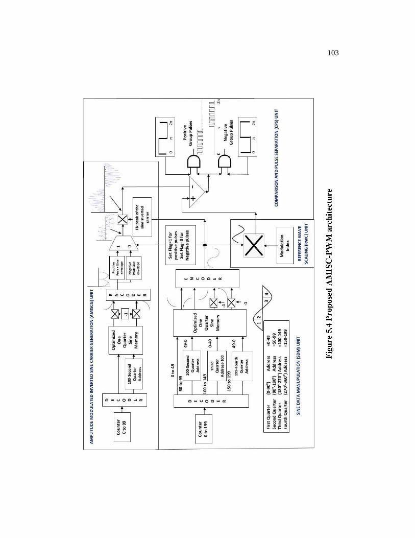
A digital architecture has been developed to implement the
AMISC-PWM technique as shown in Figure. 5.4. The architecture consists of
Sine Data Manipulation (SDM) Unit, Reference Wave Scaling (RWS) Unit,
Amplitude Modulated Sine Inverted Carrier Generation (AMSICG) Unit and
Comparing and Pulse Separation (CPS) Unit. In this novel architecture, the
modules are performing parallel. The Functionality of the units like SDM,
RWS and CPS are similar to the ISC-PWM architecture and it has been
discussed detail in the previous chapter.
The Amplitude Modulated Inverted Sine Carrier generation Unit
(AMISCGU) is designed using the VHDL as in appendix A2.3. This unit
comprises the sine generation, sine inversion and peak correction. The
function of this unit up to sine inversion is similar to the ISC-PWM method.
The amplitude of inverted sine (carrier) can be modulated by limiting the peak
of this wave by peak correction method as given in the algorithm.
103

104
5.3.1 Algorithm for Amplitude Modulated Inverted Sine Carrier
Generation
step 1. Start
step 2. Calculate one quarter cycle sine data, and store it in a
Look up table.
step 3. Fix the output ac voltage frequency of the inverter.
step 4. Initialize the initial Address value=0 for Sine Look up
table.
step 5. Derive the fetching rate clock (10 KHz) from the board
clock
step 6. Fix the carrier frequency (3 KHz) and derive from board
clock
step 7. Fetch the sine data from memory and make sine envelope
step 8. Renovate sine envelope into inverted sine carrier
step 9. Fix the amplitude peak of the each carrier cycle from the
50 Hz sine reference wave
step 10. Renovate inverted sine carrier into Amplitude Modulated
Inverted Sine Carrier (AMISC)
step 11. Get the sample from sine memory based on present
address.
step 12. Check whether carrier address reaches sampled sine data.
step 13. If reaches, and decrement the addresses.
105
step 14. Check whether addresses reach base value of sine carrier
wave.
step 15. Compare the Amplitude modulated inverted sine carrier
with presents sine reference.
step 16. If sine reference is high then decrease the PWM pulse.
step 17. If reaches the address value, increment the address for
sine sample, and go to step 8.
step 18. For 50th sample address decrement the sine sample
address
step 19. Then go to step 8.
5.4 SIMULATION AND SYNTHESIS
The functional simulation of the designed AMISC-PWM
architecture has been carried out using the Modelsim software. Using the
Xilinx ISE tool, the functional verification of the design has been done.
5.4.1 Functional Simulation
The gating pulses generated by the VHDL design for the positive
and negative group switching devices of inverter have been analyzed in the
Modelsim software. The gating pulses generated for the modulation indexes
of 0.4 and 0.8 are shown in Figure 5.5 and Figure 5.6 respectively.

106
Figure 5.5 Modelsim output pulses for Ma = 0.4
Figure 5.6 Modelsim output pulses for Ma = 0.8
107
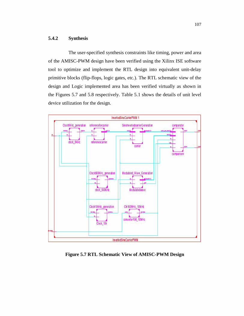
5.4.2 Synthesis
The user-specified synthesis constraints like timing, power and area
of the AMISC-PWM design have been verified using the Xilinx ISE software
tool to optimize and implement the RTL design into equivalent unit-delay
primitive blocks (flip-flops, logic gates, etc.). The RTL schematic view of the
design and Logic implemented area has been verified virtually as shown in
the Figures 5.7 and 5.8 respectively. Table 5.1 shows the details of unit level
device utilization for the design.
Figure 5.7 RTL Schematic View of AMISC-PWM Design

108
Figure 5.8 Logic implemented area for the AMISC-PWM Design
Table 5.1 Unit level Device Utilization for the AMISC-PWM Design
Mod
ule
Nam
e
RA
M(s
ingl
e-po
rtdi
strib
uted
Rea
dO
nly)
Add
ers/
Subt
ract
ors
Reg
iste
rs
Com
para
tors
(32
bit)
Mul
tiple
xers
Mul
tiplie
r
Cou
nter
30x3
2
256x
11
3bi
tadd
er
32bi
tadd
er
12bi
tsu
btra
ctor
32bi
tadd
-sub
1bi
t
1-bi
t2-to
-1
11-b
it2-
to-1
21-b
it2-
to-1
32-b
it2-
to-1
11x1
0
32x3
2
3bi
tup
coun
ter
32bi
tup
coun
ter
32bi
tup
-dow
nco
unte
r
SDMU/ RWSU
1 35 1 1 1 2
AMISCGU 1 1 1 1 100
3 4 1 3
CPSU 13 1 2 1
Miscellaneous glue logic
1 5 1 1 1
Over all Utilization
1 2 1 5 1 2 149
1 2 4 1 4 1 1 1 5 1
109
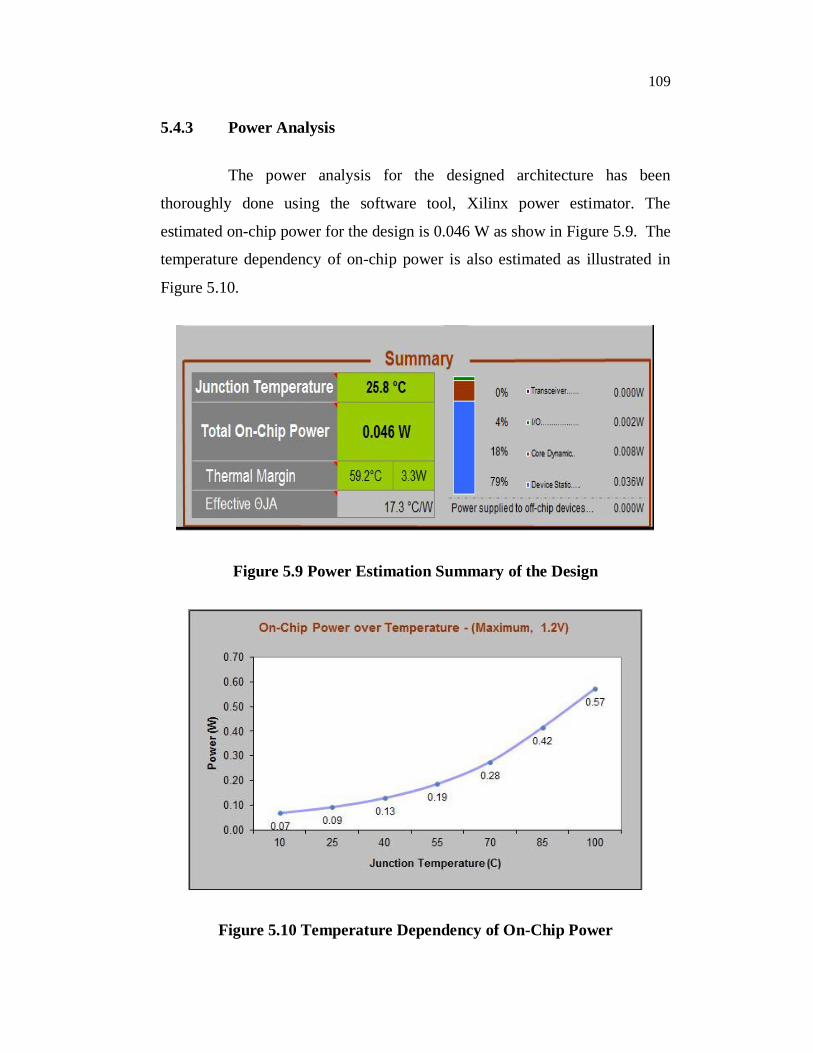
5.4.3 Power Analysis
The power analysis for the designed architecture has been
thoroughly done using the software tool, Xilinx power estimator. The
estimated on-chip power for the design is 0.046 W as show in Figure 5.9. The
temperature dependency of on-chip power is also estimated as illustrated in
Figure 5.10.
Figure 5.9 Power Estimation Summary of the Design
Figure 5.10 Temperature Dependency of On-Chip Power

110
5.5 HARDWARE IMPLEMENTATION AND RESULTS
The FPGA based AMISC-PWM architecture has been tested with a
prototype of single phase Voltage Inverter as in appendix A3.2 and the output
has been recorded and analyzed using Digital Storage Oscilloscope. The
experimental setup for the hardware implementation is as shown in Figure
5.11. The FPGA generated pulses are shown in shown in Figure 5.12. The
output voltage across the load and the frequency spectrum have been achieved
for the modulation index (Ma) = 0.8 and frequency ratio (Mf) = 15 with an
input voltage (Vdc) of 150V as shown in Figure 5.13 and Figure 5.14
respectively.
Figure 5.11 Experimental Hardware setup

111
Figure 5.12 FPGA generated ISCPWM pulses
Figure 5.13 Output voltage across the load

112
Figure 5.14 Frequency spectrum of AMISC-PWM
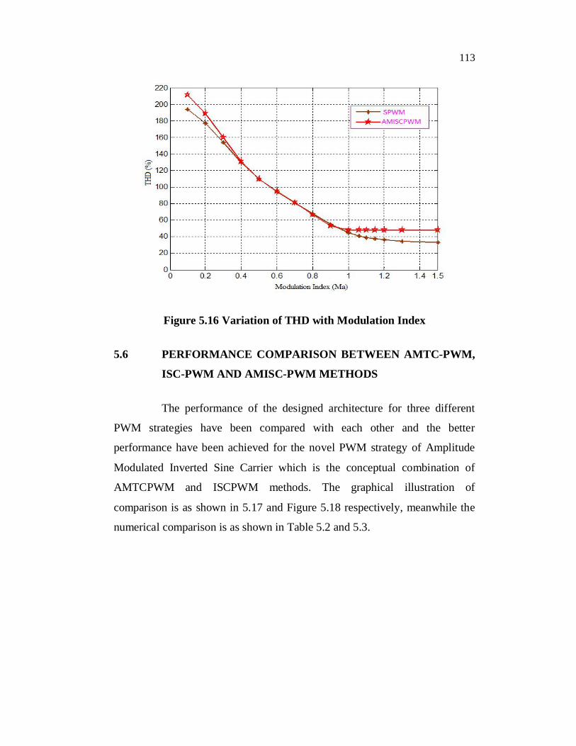
The performance of the novel AMISC-PWM strategy has been
compared with the conventional SPWM method and it results a better
performance enhancements in terms of Fundamental and THD for different
values of modulation indexes (Ma) as shown in Figure. 5.15 and 5.16
respectively.
Figure 5.15 Variation of Fundamental with Modulation Index
113
Figure 5.16 Variation of THD with Modulation Index
5.6 PERFORMANCE COMPARISON BETWEEN AMTC-PWM,
ISC-PWM AND AMISC-PWM METHODS
The performance of the designed architecture for three different
PWM strategies have been compared with each other and the better
performance have been achieved for the novel PWM strategy of Amplitude
Modulated Inverted Sine Carrier which is the conceptual combination of
AMTCPWM and ISCPWM methods. The graphical illustration of
comparison is as shown in 5.17 and Figure 5.18 respectively, meanwhile the
numerical comparison is as shown in Table 5.2 and 5.3.

114
Figure 5.17 Comparison - Modulation index Vs Fundamental Voltage
Figure 5.18 Comparison - Modulation index Vs Total Harmonic Distortion

115
Table 5.2 THD and Fundamental Comparison for Modulation Index 0.6
Method THD% Fundamental h3 h5 h7 h9
SPWM 96.82 170 0.74 0.54 0.73 0.73
ISCPWM 78.42 248 13.99 6.72 4.09 3.64
AMTCPWM 96.32 243.23 13.95 9 6.32 4.9
AMISCPWM 78.32 300 37.54 23.18 17.34 14.63
Table 5.3 THD and Fundamental Comparison for Modulation Index 1.0
Method THD% Fundamental h3 h5 h7 h9
SPWM 43.23 300 0.42 0.28 0.07 0.31
ISCPWM 43.17 330.5 36.75 17.58 11.35 8.21
AMTCPWM 45.74 375.62 98.15 54.66 35.03 23.53
AMISCPWM 45.81 375.76 111.85 67.60 48.85 38.7
5.7 SUMMARY
The major expectation from any PWM strategy is the voltage
linearity, harmonic distortion, and maximum obtainable output voltage. The
proposed architecture of novel AMISCPWM has produced a high output
voltage and low THD. The architecture developed for generating the novel
carrier function provides a high degree of flexibility in the digital
implementation. The FPGA based AMISCPWM architecture is capable of
producing the pulses with high resolution and better reliability due to its
parallel computational nature. This PWM strategy has exhibited a better
hardware realization with a single phase VSI. The comparative analysis
between the other modern PWM strategies showed that the proposed novel
PWM strategy is suitable for the system which needs a high output voltage.