Embed Size (px)
Citation preview

andreikolmakovnistgov
1
Chapter 4 Membrane Based Environmental Cells for SEM in Liquids Andrei Kolmakov National Institute of Standards and Technology Gaithersburg MD 20899-6204
Content Part 41 Introduction
411 Motivation and terminology 412 Why SEM (differences perspectives and limitations)
Part 42 Basics of SEM through the membranes 421 Image formation mechanism Detectors 422 Signal quality and spatial resolution
Part 43 Few examples of environmental cell designs and liquid SEM applications 431 QuantomiX WETSEM capsule design
432 Applications examples 4321 Water remediation 4322 Phytotoxicity
4323 High radiation dose effects
433 Prospective improvements of QuntomiX WETSEM capsules
434 Example of a custom design of the E-cells for electrochemical studies in liquids Fluidic and flow cells for SEM in liquids
Part 44 Novel 2D materials as electron transparent membranes for liquid SEM cells 441 Why do we need them 442 Preparation of the graphene and graphene oxide membranes 443 Graphene and GO based E-cell design 444 SEM imaging with GO and Graphene membranes 445 Radiation and chemical stability of the graphene based membranes
Outlook Acknowledgements References
andreikolmakovnistgov
2
Part 41 Introduction
411 Motivation and terminology Environmental electron microscopy and Scanning Electron Microscopy (SEM) in liquids are among the
most active research areas in modern electron microscopy and spectroscopy Research interest in these
techniques is broad as they enabling nanoscale research of dynamic systems in diverse fields such as
materials science biological medical and environmental sciences
Complementing conventional high vacuum SEM (Fig 1a) three schemes enable electron
microscopy in liquids and dense gases These distinct instrumentation techniques include SEM
microscopes that employ differentially pumped environmental cells (also often called as ldquoopen cellsrdquo) In
such systems elevated vapor pressure or fluidic regions of interest are separated from the high vacuum
of the microscope and detectors by multi-stage differential pumping through small apertures (Fig 1 b)
Placement of the pressure limiting apertures into the column of the microscope allows elevated pressure
inside the entire SEM sample chamber Modern commercial environmental SEM (ESEM) employs the
latter methodology enabling instrument operation at elevated pressure sufficient to maintain up to a few
kPa of gas or vapor near the sample12 This class of instrumentation is known as ESEM variable pressure
SEM (VPSEM) or low vacuum SEM (LVSEM) By cooling water vapor within the instrument nanoscale
imaging of fluid is possible using ESEMSTEM within the microscope chamber3 An alternative approach
uses molecular impermeable electron transparent membranes to isolate samples at atmospheric pressure
or in liquids from the high vacuum of the microscope4 Such environmental cells (also often called as
ldquoclosed cellsrdquo) filled with liquid gases or fluids can be placed inside the microscope chamber enabling
liquid SEM (LSEM) or wet scanning electron microscopy (WETSEM)5 (Fig 1c) Finally the third method that
enables electron microscopy instrumentation approach to imaging vapor or liquid specimens seals the
entrance of the objective lens of the SEM with electron transparent membranes thus isolating the column
and electron detectors from ambient atmosphere This technique enables realization of true atmospheric
pressure SEM (ASEM) or AirSEM where the electron beam can probe a proximal object at ambient
atmosphere conditions6-8 as shown in Fig 1d
The historical development of the membrane based transmission electron microscopy (TEM) is intriguing and enlightening More than seven decades of development of such liquid cells from early work on collodion membranes by Abrams and McBain4 until recent state of the art monolithic Si based chips for microfluidic electron microscopy9 are described comprehensively in Chapters 1 and 2 of this book This chapter concentrates on the development capabilities and applications of membrane based SEM in liquids describing the advantages and limitations of the technique This field is an increasingly active research area and at this point in time no versatile commercial product exists to meet the diverse experimental needs of the research community The chapter thus discusses ongoing research efforts based upon custom fabricated instrumentation that improve the capabilities of membrane based environmental cells (E-cells) We will use the terms liquid SEM membrane SEM WETSEM or ambient pressure scanning electron microscopy (APSEM) through the chapter to refer to this technique unless specified implying that both dense gaseous and liquid media may be used with this technique
412 Why SEM (differences perspectives and limitations)
andreikolmakovnistgov
3
The great majority of the electron microscopy research in liquids and gases is based upon use of (S)TEM thanks to its great spatial resolution and analytical power or ESEM In spite of somewhat lower resolution the membrane based liquid SEM has its specific niche thanks to a) High surface and near surface sensitivity enabling high
resolution analysis of interfacial processes
b) Wider pressure and temperature ranges that can be
achieved independently inside closed cells The latter are only
limited by the mechanical stability of the membranes and
pressure differential of few Bars can routinely be achieved
b) Closed E-cells enable research of chemically reactive toxic
or even radioactive media without contamination of the main
chamber of the microscope
c) Unique or precious samples can be studied without losing
them due to sublimation or evaporation process
d) As opposed to TEM techniques there are fewer limitations
of the imaged sample size Membrane based SEM techniques
enable both large lateral fields-of-view (FOV) of up to a few
mm2 as well as facile incorporation of optical electrical micro-
mechanical fluidic and other connectors As a result SEM
based membrane techniques meet the requirements for correlative optical microscopy and spectroscopy
f) Finally this methodology can be adapted by a large number of scientists using standard SEM
instruments
Part 42 Basics of SEM through the membranes 421 Image formation mechanism Detectors The processes occurring during electron beam interactions with objects inside liquid cell can be best illustrated with Monte Carlo simulations of electron trajectories10 (Fig 2 a b) When a high energy electron probe beam with energy Eb impinges upon the membrane and enclosed liquid specimen the primary electrons dissipate their energy and change the directions via multiple inelastic and elastic processes As a result the electrons ions radicals and electronic excitations become distributed within the interaction volume (defined by colored trajectories in the Figure 2a) whose dimensions depend on primary energy of the beam properties of the membrane and the media behind the membrane as well as probesurface interaction angle One of the commonly used parameter to estimate the dimensions of the interaction volume is the electron range
119877119870119874 asymp28∙119882
119885089∙120588 119864119887
164 [119899119898] (41)
parameterized by Kanaya and Okayama11 (here W [gmol] is the atomic weight Z is atomic number and ρ [gcm3] is the density of the media) For example liquid water enclosed behind a 30 nm SIN membrane yields RKO that ranges from ca 50 nm to ca 2000 nm for 1 keV and 10 keV primary electrons correspondingly (see Fig 2 a) While secondary electrons (SE) originate from the first few nanometers of the membrane it is important to note that ca 90 of backscattered electrons (BSE) originate within ca 01 RKO (for high Z materials) to 03 RKO (for light elements) 12 Thus for liquid SEM imaging the RKO parameter (and its energy
Figure 1 a) Standard high vacuum SEMTEM setup HV PESE and TE stand for high vacuum primary electrons secondary electrons back scattered electrons and transmitted electrons correspondingly b) open cell environmental SEMTEM c) closed cell environmental SEMTEM d) atmospheric pressure SEM
andreikolmakovnistgov
4
dependence) has crucial importance since it determines the ultimate ldquoprobing depthrdquo in liquid and therefore the contrast and resolution of the resultant images Consider high Z object A (eg Au nanoparticle) being immersed into low Z liquid background B which is separated from high vacuum of electron beam and detectors space by thin membrane m (as in
the figure 2 a b) Assuming the standard SIN membrane thickness being few tens of nanometers low energy secondary electrons (SE) from the object behind the membrane will be completely attenuated The signal (S) detected by standard cumulative SEBSE electron detector from such an object as the following contributions
S=SEm+BSEm+BSEs+SEs (42) (Fig 2 c) which includes SE and BSE electrons from the membrane (subscript m) and sample (subscript s) behind the membrane Note that SEs component (often called SE type 2 electrons or SE2) originates from backscattered electrons BSEs scattered from sample in the direction of the incident of the probe beam These BSEs excite detectable SEs from the membrane The total yield of backscattered electrons η (also called backscattered electron coefficient) will be
η= ηm+ ηs (43) Similarly the secondary electron coefficient is
δ= δm +Δmiddotηs (44) (here sub-indexes s m correspond to membrane and sample respectively and Δ coefficient is an efficiency of secondary electron emission from the membrane by outgoing BS electrons emitted from the sample) Electron detector efficiencies εSE εBSE enables the cumulative electron signal formula to be written
S= εSE (δm +Δmiddot ηs) + εBSE middot ( ηm+ ηs ) (45) The contrast C between two points A and B in SEM image Figure 2 is defined5 as
C=(SA-SB)SA and can be reduced to C= (ηsA- ηsB) ηsA (46 a b) assuming both sufficiently high energy (few keV) of primary electron beam penetrating few tens of nanometers thick membrane and featureless signals from the membrane and from liquid backgrounds Under these conditions SEM contrast is predominantly determined by the ratio of the backscattered electron coefficients of the object and the liquid emphasizing the importance of backscattered detectors
Figure 2 a) Electron trajectories of a 10 keV electron beam in water after beam passes through a 30 nm SIN membrane
The electron range 119877119870119874 is marked with the dashed line b) the drastic change of electron trajectories after probe beam
interacts with 200 nm Au nanoparticles immersed in water 100 nm below membrane backscattered electrons (BSE)
enables image formation of objects in liquids c) The major electron signal formation mechanisms during membrane based
SEM in liquids includes secondary electrons (SE) and BSE due to membrane (m) and sample (s) interaction
10 keV
water
Au NP 200 nm
BSE
SINA
30 nm SIN membrane
B
RKO
1 microm
a) b) Ib SEm
BSEm
BSEs
SEs
membrane
liquid
sample
c)
andreikolmakovnistgov
5
for membrane based SEM The validity of these considerations has been verified by Thiberge etal experimentally through use of liquid cells equipped with 145 nm thick polyimide membranes5 One of their revealing experimental results describes the energy dependence of the ratio T= (ηsmiddot(1+ Δ)) ηs theor (47) as shown in Fig 3 The numerator of this equation denotes the sample signal (without featureless membranersquos terms) experimentally recorded through 145 nm polyimide membrane while the denominator describes the theoretical values of ηs theor for the membrane material Since this is a ratio of the amount of BSE transmitted through the membrane to the theoretically
expected total this dimensionless parameter has minimal material dependence and defines the electron transparency of the particular membrane Several important conclusions can be deduced from the analysis of these experimental dependences a) The experimental electron transmittance curves of the membranes have a characteristic transparency threshold indicating for example that 145 nm thick polyimide membranes are practically opaque for electrons with energies below 4 keV as shown in Fig 3 This transparency threshold is not a constant value but can be reduced for low probe beam energies by decreasing thickness andor density of the membrane material b) The transmittance curve shape also depends on the media behind the membrane For a water sample (eg low Z material) the electron transmittance of the polyimide membrane is systematically lower compared to gold (eg high Z) one (Figure 3) The latter can be a consequence of so-called Z-filtering effect of the membranes which are actually more transparent for samples with higher Z number5 This is a feasible explanation since for any given energy of the primary electron beam Eb the maximum of energy spectra of the backscattered electrons from high Z targets is centered closer to Eb compared to one for light materials which peaks at ca Eb2 Thus electrons from the low Z targets become more attenuated by the membrane on their way out to the detector c) The presence of the apparent maximum in transmittance curve for Au and its value in excess of 1 can be attributed to the significant contribution of SE2 electrons to the total detectable signal from the sample Further increase of energy of the BSEs reduces the cross section for SE2 generation implying that an optimal condition exists for signal generation and contrast that enables both BSEs and SE2 detection of objects from beneath the membrane 422 Signal quality and spatial resolution The attenuation of the primary beam electrons and BSE signal by the membranes raises the question of probe beam currents required to generate sufficient contrast from objects immersed in liquid behind the membrane This is also important question from the samplersquos stability point of view since elevated beam currents generate image artifacts degrade samples and complicate interpretation of
Figure 3 Energy dependence of the 145 nm thick polyimide membrane electron transparency as a function of primary electron energy and material behind the membrane Notice the existence of the characteristic transparency threshold and abnormal transparency around 10 keV for high Z material Aadapted from Ref [5]
andreikolmakovnistgov
6
experimental results (see section 323 as an example) A measure of image contrast is based upon the Rosen criteria stating that the signal difference between points (subscript A and B) should be (SA-SB) gt 5n12 to yield reliable imaging of the object A behind the membrane over the background B (Fig 2a) where n is the quantity of electrons reaching the detector12 The latter can be translated5 in to so-called threshold equation
119868119861 gt16
1205781198781198791198622 [119901119860] (48) where ηS is the
backscattering coefficient of the sample under the membrane T is the time to complete image scan (in seconds) and C= (ηsA- ηsB) ηsA is a contrast between the sample and background Using (48) equation Thiberge etal5 calculated the minimal SEM beam current needed to image characteristic objects immersed in water (Table 1) The data shows that reliable imaging of samples like living cells with effective Z numbers and back scattered coefficients close to water require more than four orders of magnitude
larger beam current compared to materials with larger Z as gold Potentially this is a limiting factors of the liquid SEM of unstained living cells since such this radiation doses would lead to direct radiation damage of the cells or their indirect degradation due to series of chemical reactions induced in surrounding water (see also sections 323 and chapters 7 16 18 24)
Material Z η Contrast to water IB (pA)
Water 722 0075
Cells 707 0073 0027 2900
Oil 58 0055 0267 30
Gold 79 078 09 025 Table 1 Calculated minimal SEM beam current needed to image few characteristic objects immersed in water using threshold equation Scanning time T=100 s and η values for 20 keV were used adapted from Ref [5]
andreikolmakovnistgov
7
The diameter of the primary electron beam broadens due to scattering by the membrane and enclosed liquid media (Fig 4a) thus probe beam diameter increases with increased sample depth Probe beam diameter increase in liquid cell SEM was analyzed both theoretically and experimentally by Thiberge et al5 Effective electron beam diameter in the liquid is described as
119889119890119891119891 = radic1198891198872 + 119889119898
2 + 1198891199081198861199051198901199032 (119905) (49)
(here db is an electron beam diameter dm is beam broadening due to scattering inside the membrane and dwater (t) ndash beam broadening while passing the water layer of thickness t) From Monte Carlo electron trajectory simulations for dwater(t) the authors determined the beam diameter as a function of depth for the object in water as shown as Fig 4b This equation implies that the beam diameter is expected to be as large as 100 nm at ca 400 nm below the surface of standard 145 nm polyimide membrane and two objects separated by 200 nm would barely be resolved at these conditions In practice the experimentally observed resolution for objects with Z gt Zwater was found to be much better compared to simulated one and the latter one can be seen as a lower limit This improvement in resolution is attributed to much higher
electron scattering from high Z objects immersed in water compared to water background In this case resolution is not defined solely by incident probe beam diameter in water (as it would be the case for the object with comparable Z) but mainly by the size of the object and by dramatic increase of the BSE signal when beam hits the object (compare BSE yield in Figures 2a and 2b) To illustrate this point the simulated
SEM images of the two separated 200 x 200 nm2 1 m long Au rods are depicted in the Figure 4c as a function of the water layer thickness between 30 nm SiN membrane and the sample The simulation demonstrates that two strongly absorbing high Z objects can be resolved up to two microns from the membrane using 30 keV primary electrons In general the broadening of the electron beam in liquid leads to the rule of thumb (see Ref5 ) that high Z objects can be detected if their size is comparable to the local size of the beam in liquid The contrast from the object whose size is two-tree times smaller than the broadened beam diameter reduces the SNR of the imaged object This effect is illustrated by simulating image conditions of the particles When beam diameter exceeds the size of the nanoparticle (at the depth above 600 nm) both the resolution and contrast deteriorate quickly as shown in Fig 4 c This result implies a limitation on maximal depth where the particles of certain size can be detected and resolved It is important to note that increasing the probe beam energy improves the depth and resolving power of
Figure 4 a) Monte Carlo simulations beam broadening while passing 30 nm SIN
membrane and impinging the water layer b) Effective electron beam diameter
deff in water as a function of the probing depth (the data points were adapted
from Ref [5]) c) the simulated SEM images of the two separated 200 nm x200
nm square and one micron long Au rods as a function of the water layer
thickness between 30 nm SiN membrane and the sample
400 nm 1500 nm800 nm200 nm30 keV Au water
500 nm
water
30 nm SIN
dbeam
a) b)
c)
andreikolmakovnistgov
8
liquid cell microscopy but does not necessarily leads to optimal imaging since electron scattering cross section becomes reduced with energy and small nanoparticles even being close to the membrane would not have enough material to provide a measurable BSE signal Part 43 Few examples of environmental cell designs and liquid SEM applications
Recent progress in liquid electron microscopy is a direct result of success in high yield microfabrication technology of ultrathin membranes developed for MEMS devices ultrafiltration and X-rays (electron) transparent windows and development of commercial available tools for research application A number of vendors offer an array of Si SiO2 Si3N4 (SiN) SiC polyimide and other membranes with the thickness ranging from 5 nm to 200 nm which can be used for assembling custom made liquid cells To date the majority of the liquid cell SEM results have been obtained using Quantomix wet cells though alternative commercial membrane based liquid cells have become available recently13
14 In this section we describe the commercially available QunatomiX wet cells and related research that extends this instrumentation to new applications
431 QuantomiX WETSEM capsule design The development of the WETSEM technology by QuantomiX15 in early 2000s was a response to growing demand for in vivo imaging of biological tissues and live cells with spatial resolution better compared to conventional light microscopy Detailed designs capabilities and applications of this approach can be found in the literature5 15 16 The cell principal design is depicted in the Fig 5 and it consists of two parts the top sample dish with electron transparent membrane covering the sample compartment and the stub The cell can be vacuum sealed with a rubber membrane used to joining the two elements The sample compartment can be filled with ca 15 microL of liquid sample Several modifications to the conventional cell body design were proposed15 Proposed modifications include insertion of fiber optics for correlative SEM and cathodoluminescence imaging of hydrated samples16 (see Figure 5 b-d) The QuantomiX WETSEM is enabled with a robust 145 nm thick polyimide electron transparent membrane supported by metal grid The grid provides sufficient mechanical stability for the membrane to withstand atmospheric pressure
Figure 5 a) The basics of QuantomiX WETSEM capsule design b) The realization of the complementary SEM and optical imaging in WETSEM capsule via introduction of an optical fiber c) BSE image of the fully hydrated untreated CHO cells visualized simultaneously with cathode luminescence (CL) signal (d) (Adapted from S Thiberge etal PNAS 2004 101 3346-3351 Copyright (2004) National Academy of Sciences USA
andreikolmakovnistgov
9
differential and yet offers a large segmented ca 4 mm2 FOV The rubber membrane that separates the two elements of the liquid cell is a thin elastomer material that expands in vacuum and functions as a pressure relief element that reduces the risk of polyimide membrane rupture during cell closing and SEM vacuum pumping
The 145 nm thickness of the polyimide membrane implies usage of BSE with energies in excess of 10 keV for SEM imaging of wet samples (see Figure 3) Due to strong attenuation of the BSE signal by the membrane and interfacial water layers it is crucial requirement to have a sample in a close proximity or adhered to the inner surface of the membrane Thus a number of protocols that functionalize the membrane surface to promote nanoparticles adhesion as well as cells culture growth have been developed To work with wet biological tissue biopsies plants sections and other soft samples an upgraded capsule was designed15 The latter was equipped with the special spring loaded piston which gently pushes the tissue against the membrane
432 Applications examples
4321 Water remediation
Numerous studies in variety of fields have been performed using QuantomiX cells17-23 The selection of
research described in the Fig 6 demonstrates use of the wet SEM cells for in situ observation of the metal
remediation in water by TiO2 based photo catalysis24 Electron-hole pairs generated in catalysis particles
by the UV radiation from the Sun can diffuse to the surface and reduceoxidize ionic and molecular
pollutants in water such as heavy metal ions25 An example of such a photo catalytic reaction is UV photon
induced reduction of ionic Ag to metallic nanoparticles at the surface of BaTiO3 catalysis in AgNO3 water
Figure 6 a) SEM image of as prepared bare BaTiO3 photocatalyst b) similar micro particle after UV light exposure in 10-4 M
aqueous solution of AgNO3 Ag reduction can be seen on (001) facet (Adapted from ref [26]) c)-f) In situ reordered
sequential liquid SEM images of a titania whisker immersed in 10-4 M aqueous solution of AgNO3 Areas marked with circles
triangles and squares show divergent growth morphologies as a result of electron beam induced reduction of Ag ions
Imaging conditions 30kV acceleration voltage and BSE detector g) The mechanism of electron beam induced reduction of
Ag ions at the surface of TiO2 h) blue curve corresponds to EDS spectra recorded from AgNO3 solution and red from Ag
decorated TiO3nanowire Adapted with permission from N Kolmakova and AKolmakov J Phys Chem C 2010 114 (40) pp
17233ndash17237 Copyright (2010) American Chemical Society
andreikolmakovnistgov
10
solution26 Fig 6 a b demonstrates an ex
situ SEM comparison of BaTiO3 photo
catalyst before and after illumination with
UV light Since BaTiO3 is ferroelectric it has
a spontaneous polarization which affects
the chemical reactivity of different crystal
facets As can be seen in the Fig 6b Ag
becomes deposited only on (100) facet
implying that the internal polarization
promotes the photo catalytic action to
occur predominantly at this interface26
Observation of such a process in situ is
possible using QuantomiX WETCELL
instrumentation In this case TiO2 single
crystal whiskers are adhered to the liquid
cell inner membrane and in either a pure
water or ca 10 microL of 10-4 M AgNO3 aqueous
solution was dropped into the E-cell
compartment No changes occur in
morphology and shape of the titania
nanostructure as a result of exposure to a
30 keV electron beam in pure water
Conversely imaging TiO2 single crystal
whiskers in an AgNO3 solution shows the
TiO2 nanostructure becoming progressively
decorated with metal particles as depicted in Fig 6 c-f The origin of this phenomenon is similar to photo
catalysis and is due to electron induced reduction of the Ag ions from the solution at the surface of the
TiO2nanostructure The difference between these two experiments is that electronndashhole pairs are created
in TiO2 by the primary electron beam in the liquid cell system Assuming that the stoichiometry of the
electron induced reaction taking place at the surface of TiO2 nanowire submerged in AgNO3 solution is
analogous to the classical photocatalytic reaction (photoreduction) 27 one can write
2 0
2 24 2 4 4TiO
e beamAg H O Ag O H
(410)
where the first frac12 reaction is a transfer of an excited electron to the Ag+ bound to the TiO2 surface leading to the growth of Ag0 domains with high quantum yield The hole transfer to the surface-bound water or hydroxyl groups completes the second frac12 reaction The diagram of the electron induced silver deposition process is depicted in the Fig 6g Evolution of the EDS spectra before (blue curve) and after (red) nanoparticle particle growth demonstrate the accumulation of Ag depositions on the nanowire and the feasibility of recording of EDS spectra on objects in liquid cells
4322 Phytotoxicity The growing production of nano-enabled materials such as engineered nanoparticles (ENP) raises
concerns regarding waste byproduct and potentially negative ENP impacts on human health and
Figure 7 a) The anatomy of Arabidopsis root tip (b c) laser scanning confocal microscopy of Arabidopsis root tip exposed to 270 microgL of 40 nm Ag NPs for 4 weeks panels b) and c) represent the surface (8 microm below the root surface) and semi-median (ca 36 microm below the root surface) scans correspondingly showing distribution of AgNPs in larger root cap cells epidermis and columella initials d) NP decorated Arabidopsis roots imaged with SEM in water e) Higher resolution SEM images of fully hydrated Arabidopsis root cup cells with visible interior (nucleolus) and Ag nanoparticles decorating cellular walls Adapted from ref [29]
andreikolmakovnistgov
11
ecosystems Plants are direct or indirectly consumed element in the human food chain motivating the investigation of the uptake and accumulation of ENP by plant roots and leafs Therefore an application of liquid SEM is ENP phytotoxicity on living plants We test the capabilities and limitations of this imaging modality to probe the in vivo uptake and accumulation of nanoparticles and metal ions by plants at the cellular level A recent example of such an approach is a study of cellular accumulation and subcellular transport of Ag nanoparticles in Arabidopsis thaliana28 Arabidopsis root anatomy is well understood (Figure 7a) and is often used as a model pant system In this experiment a diluted Ag nanoparticles-water colloid was added to a hydroponic nutrient solution (Hoagland solution) where seeds of Arabidopsis thaliana where germinated and different sizes and concentrations of Ag ENPs were tested After controlled growth and uptake the tips of the plant roots were sectioned in a wet state and adhered to the back side of the electron transparent membrane of the QuantomiX WETSEM and cell was filled with water Figs 7 b c shows two laser scanning confocal microscopy optical sections of the root tip exposed to 40 nm Ag ENP and recorded at near surface and at the median part of the root correspondingly Correlative liquid cell SEM images are depicted in the Figs 7 d e Significantly improved resolving power and signal to noise (SNR) ratio from the WETSEM instrumentation reveal that after two week of roots exposure to ENP the accumulation predominantly takes place at root cap at columella cells and border cells28 At low concentrations and exposure times the cell walls of those are coated with individual nanoparticles at surface densities sufficient to impede incoming solute transport The detailed SEM image analysis of the intercellular regions (supported with ex situ TEM studies) indicated the presence of Ag NPs aggregation at plasmodesmata connecting adjacent cells Ag ENP aggregation at plasmodesmata may lead to blockade of the symplastic transport between cells and thus degrade system viability
4323 High radiation dose effects In spite of the demonstrated advantages of liquid cell SEM for high resolution analysis of ENP fate
in plants limitations exist for application of this technique to biological objects Inelastic interaction of the probe beam with liquid water and biological material results in the generation of a variety of ionized and excited molecular species in the interaction volume (see chapters 7 9 and references therein29 ) As a result steady state concentrations of strongly reducing and oxidizing species such as hydrated electrons (eh
minus) hydroxyl radicals (OHbull) hydrogen peroxide H2O2 hydrogen radicals (Hbull) H3O+ as well as molecular hydrogen and oxygen (H2 O2) are formed in and around the interaction volume Assuming that that the radiation dose rate in standard SEM measurements is somewhat larger (ca 108 to 109 Gys) compared to
Figure 8 a) Liquid SEM image of Arabidopsis thaliana with cellular walls decorated with 60 nm Ag nanoparticles b) c)
Electron beam induced Ag nanoparticles dissolution and plant tissue degradation in water with growing radiation dose d)
Two order of magnitude increase of the beam intensity at specified locations reverses the process and results in Ag0
redeposition on membrane inner surface
andreikolmakovnistgov
12
TEM case (ca 108 Gys) and following the scaling laws deduced in ref 29 one can expect the steady state molar concentrations of OHbull and H2O2 species to be in excess of 10-4M The radiolysis byproducts from probe beam illumination contribute significantly to chemical stability of nanoscopic objects in solution and degradation of biological samples An example of the probe beam induced degradation of fully hydrated biological tissue is shown in the Fig 8 Here panels a b and c show a selection of sequential liquid SEM images of the root cup of Arabidopsis thaliana immersed in water following incubation in Ag ENP Similar to Fig 7 nanoparticles accumulate at root cup cell walls and are immobilized Significant degradation of the cell walls can be observed following low dose SEM imaging (ie 10 enm2) while continued exposure leads to complete decay of the cell walls (Fig 8 c) evidenced by reduced image contrast as well as release and dissolution of decorating 60 nm Ag nanoparticles
Noticeably increasing the dose by two orders of magnitude for the same solution by increasing scanned probe beam dwell times results in aggregation of Ag on to the back side of the membrane (Fig 8 d) This interplay between ENP dissolution and growth phenomena as function of electron dose rate can be explained by the radiolysis conditions driven by the incident probe beam Local redox reactions with participation of metal ions are controlled by relative concentrations of primary reducing (eh
minus) and oxidizing (OHbull) agents (see chapter 7 of this book) The relative concentration of solvated electrons increases with incident probe beam electron dose driving reduction of Ag+ + eh
minus Ag0 and growth of Ag depositions At lower beam intensities the opposite process occurs where metal dissolution prevails The probe beam dose borderline between deposition and dissolution was determined to be between 10-9 and 10-10 Gys for TEM experiments a value close to SEM dose imaging conditions
These recent findings will help better control of the probe beam induced nucleation and growth processes in liquids as well as promote the development of SEM electron beam induced deposition (EBID) process in liquids reviewed in Chapter 1430 Coupled with electrochemistry the latter process will have drastically increased selectivity and deposition yield compared to its vacuum analog Furthermore a much greater moiety of chemical and bio species can be used for EBID in liquids Flushing of gas or liquid media inside E-cell can be easily done without braking SEM vacuum enabling nanoscopic sequential deposition of different chemical species in the system
433 Prospective upgrades of QuntomiX WETSEM capsules
andreikolmakovnistgov
13
Currently the QuantomiX WETSEM capsules are mainly used by the bio-medical research
community and the usage of these E-cells for materials research is limited Adoption of this instrumentation by the materials community is restricted by the limited capabilities of these capsules to vary the temperature of the imaged sample as well as altering in situ its chemical and electrical (electrochemical) environment Development of these capabilities would broaden the utility of WETSEM systems for martial science application Our Initial efforts to develop these instrumentation capabilities is depicted in the schematics of Fig 9 where central stub of QuantomiX QX-302 capsule has been modified to be used for connection of multiple electrical leads and tubing for gas or fluid delivery Use or removal of the metal coating of the standard capsule stub assembly enables control of electrical connections to the capsule and fluid solution while vacuum sealing of electrical leads and fluidic tubing is enabled by application of UV curable glue
Thermal control over the sample environment was enabled through development of a simple heating and cooling system based upon a miniature 4 W Peltier element and copper heat sink (Fig 9a)31 In this system the heat from the thermoelectric module is delivered to the electron transparent membrane using a copper bar connecting the membrane supporting metal grid of the capsule to the thermoelectric module The bar is spring loaded against the membrane supporting mesh and maintains thermal contact with the grid while enabling capsule assembly and disassembly Using this setup temperatures as low as -10 degC and as high as 100 degC can be achieved at the membrane (Fig 9b) The use of more powerful thermoelectric elements enables a larger range of system temperatures
The ability to cool or to heat samples in their native gaseous or liquid environments at a variety of pressures opens new possibilities in SEM which cannot be achieved using commercially available cryo- or heating stages For example the particularities of water condensation wetting and flow in 3D photonic structures enable understanding the fundamental processes controlling optofluidics32 33 and sensorics34
Figure 9 a) Customization of QuantomiX capsule with addition of heatingcooling electrical and fluidic capabilities
b) Temperature of the sample supporting membrane in (a) as a function of power of the 4W thermoelectric element
c) consequent liquid SEM images of water condensation at Morpho butterflies scale upon cooling inside water vapor
filled QuantomiX capsule (see details in the text and in ref [32])
andreikolmakovnistgov
14
Fig 9 c shows mesoscopic details of initial stages of water condensation at the surface of natural photonic structure butterfly wings The butterfly scales were adhered to the back side of electron transparent membrane which can be heated or cooled inside the QuantomiX capsule The capsule contained the water droplet separated from the membrane thus dew can be formed or evaporated via cooling or heating the membrane loaded with butterfly scales Panel 1 of Fig 9 c shows a SEM image of the characteristic mesoscopic ridge structures of a stacked periodic layers of cuticle separated by the air gaps of a dry Morpho butterflies scale For comparison panels 2 and 3 of Fig 9 show sequential images of the same region upon cooling in the presence of water vapor In this figure water first condenses at the top of the ridges after which the condensation front spreads along the ridges As recently discovered this particular condensation pattern is due to existing gradient of surface polarity along the height of the ridge from the polar ridge tops to the non-polar bottoms35 The water therefore preferably condenses and spreads along the top part of the ridges leaving air pockets deeper inside the scales resulting in a hydrophobic wing structure that allows the butterfly to shed water droplets Note that the improved lateral resolution of this process is achieved using conventional ESEM vs a liquid cell system However the former approach does not allow decoupling of thermal and pressure induced processes and has limited pressure range
434 Example of a custom design of the E-cells for electrochemical studies in liquids Increased functionality of the environmental cells used for electron microscopy is a current trend
in TEM and STEM studies Several types of fluidic heating and electrochemical cells have become available recently36 37 And many of the commercially available or custom developed E-cells for (S)TEM can be directly adapted to SEM research as well14 38 The latter approach however is rarely adopted by SEM community since the core advantage of the SEM large field of view fast exchange and analysis of arbitrary samples cannot be easily implemented in thin TEM flow cells with characteristic submicron fluidic flow channels As a result several custom made E-cells specifically designed for complex SEM studies have been reported39-41 One of these simple and cost effective instruments is described below
Recent energy and environmental initiatives resulted in growing application of SEM in liquids and dense gases including research into morphological and compositional alterations of nanoscopic devices
andreikolmakovnistgov
15
and interfaces during operation in realistic environmental conditions In many research settings there often require variety of objects within the imaged FOV for comparative or combinatorial analysis The latter experiment requires development of the complex circuitry on electron transparent membrane and parallel indexing of multiple electrodes A practical solution to this experimental challenge is to employ SiN membrane widows on SiNSi chip with lithographically defined electrodes array Such an electronic chip-with-a window can be wire bonded to standard vacuum compatible ceramic chip carrier (Figure 10 ab ) requiring only slight modification such as a millimeter size hole through the center of the device39 For electrochemical studies the surface of the electrical leads and other metal surfaces are coated with SiO2 insulating layer as shown in Fig 10 b The assembly can be used in two different setups For
correlative optical and electron microscopy the 70 L cavity was filled with a 1 mM solution of AgNO3 to act as a model electrolyte and covered with a glass lid sealed to the device with UV curable adhesive The glass lid acts as a viewing port making the cell usable with both optical and SEM thus enabling correlative microscopy analysis Alternatively the fluidic chamber can be attached to the chip carrier (Figure 10 c d) to enable exchange of the solution within the device Fig 10 e shows a cyclic voltammogram of Ag plating (stripping) from AgNO3 water solution on to (from) SnO2 nanowire wired as a working electrode The
Figure 10 Design and results of multi-electrode electrochemical cell that enables in situ electrochemical studies in
liquid using SEM and optical microscopy a) standard ceramic chip carrier equipped with electron transparent SiN
window b) the electron transparent window with multiple electrodes for electrochemical SEM studies in liquid
electrolytes c) and d) the picture and design of the corresponding fluidic cell e) the voltammogram of Ag plating
and stripping atfrom SnO2 whisker immersed in 10-3 M AgNO3 solution with corresponding liquid SEM images
Adapted from ref [39]
andreikolmakovnistgov
16
corresponding in situ liquid SEM images demonstrate the morphology of Ag0 deposit from the solution as well as it complete stripping at a reverse potential An in-situ comparative energy dispersive X-ray (EDS) analysis has been recorded (not shown here) before and after the deposition of Ag supporting the deposition of pure silver on to the surface of the SnO2 nanowire
Part 44 Novel 2D materials as electron transparent membranes for liquid SEM cells 441 Why do we need them In spite of great progress in implementation of SiN SiO2 and polyimide membranes in liquid SEM (STEM) cells reduction of beam scattering and signal attenuation by the membrane itself would improve SEM image quality analytical capability and reduce electron dose into the sample The strategy to improve the scattering and transparency of the membranes are based upon the reduction of their thickness and atomic Z number of the membrane materials Commercially available SiN and SiO2 -based membranes fabricated via SiN (SiO2)Si wafer back KOH etching process are as thin as 5 nm However due to fluctuations in Si etching speed such membranes can be produced reliably with minimal windows sizes of ca 10 microns or larger With large effective diameters such thin windows are prone to mechanical collapse under the one atmosphere pressure differential in vacuum systems and are thus not ideal for liquid SEM E-cells Prospective technological approaches based upon fabrication of large-area perforated-supporting membranes with micron size orifices enable much thinner membranes Such electron transparent windows are the base of modern E-chips of ambient pressure TEM and can in principle be adapted for ambient pressure SEM studies
andreikolmakovnistgov
17
An alternative approach to reducing atomic number and membrane thickness includes novel free standing membranes42 43 made of single atomic layer two dimensional (2D) materials such as graphene graphene oxide and etc These membranes are impermeable to liquids and gasses and enable new capabilities for TEM and SEM in liquids The two major differences with respect to standard SiN or SiO2 membranes are that graphene based membranes have extremely high breaking strength44 that facilitates fabrication of atomically thin electron transparent windows such that inelastic electron mean free path
lengths in single layer graphene for an example are larger than its thickness at SEM range electron acceleration voltages We infer from this property that incoming and outgoing electrons can pass such a membrane without significant attenuation Opportunities are even more intriguing for very low energy electrons ( lt5 eV)45 For such electrons the electron-electron scattering is further hampered and electron ndash phonon scattering is inefficient Therefore for low energy secondary electrons these membranes can be nearly totally transparent Thicker multilayer membranes (eg 1 to 2 nm) have higher strength and more robust performance These membranes are thus practical for liquid SEM measurements As a result of these properties new opportunities for SEM emerge a) True SEs can be used for imaging the surfaces of objects covered with such a membrane Therefore data can be acquired from specimens at ambient pressure in fully hydrated conditions with SEM resolution and surface sensitivity b) An array of powerful surface sensitive analytical techniques such as XPS AES NEXAFS etc can be applied to such objects Additional advantages include c) Smaller primary beam energies can be used enabling smaller excitation volumes and reduced beam induced damage d) Negligible charging effects due to fast neutralization of the accumulated charge ether by conducting electrons (in G GO) or in case of dielectric membranes (eg BN) via tunneling from
the conducting liquid media e) Longer stability of the graphene membrane with respect to knock-on process since SEM electron beam energy is well below the energy threshold for graphene (~80 keV)46
The electron transparency of the 2D free standing graphene boron nitride or graphene oxide membranes or coatings was evaluated in multiple reports using TEM 43 47 48 for high energy electrons as well as point projection microscopy49 50 and SEM51 for slow ones Complementing surface science studies the electron attenuation length (EAL) parameter was used as an equivalent to inelastic mean free path assuming that elastic scattering is negligible as signal returns to the detector 52 EAL relates the initial
electron flux of secondary and back scattered electrons (I0) from objects under the membrane to the one
(I) measured by the detector
Figure 11 Experimental data points (filled circles)
represent the effective attenuation length (EAL) for
graphene monolayer from ref [56] and from ref [57]
(diamonds) In addition EAL data (diamonds) For
comparison horizontal dashed lines denote the
thicknesses of single and bilayer graphene Solid
line predicted inelastic mean free path in graphite
as calculated using TPP-2M formula [54] Adapted
from ref [56]
andreikolmakovnistgov
18
119868 1198680 = exp(minus(119871
120582119872+frasl
119889
120582119866)) (411)
here λG λM are EALs for graphene membrane and the media between the object and the membrane while d and L stand to thickness of corresponding layers as shown in the inset of Fig 11) This method is widely used to determine the thickness of overlayers for materials with known EALs53 Using this calculation EALs for graphene and graphene oxide were measured via collecting the substratersquos XPS54
55 AES56 and secondary electrons57 signals attenuated by the known amount of graphene or GO layers Fig 11 compiles some of this experimental data and compares them with theoretical predictions for carbon53 The reasonable agreement can be observed for the electrons acceleration voltages exceeding 70 eV EALs for energy ranges below this value have yet to be explored
442 Preparation of the graphene and graphene oxide membranes Graphene oxide (GO) was the first 2D material tested as an electron transparent window for SEM
E-cells54 58 The attractiveness of GO membranes stems from the well-developed high-yield GO production protocols of this material as discussed by Park and Rouff 59 and references therein Conveniently chemically exfoliated GO flakes have hydrophilic edges due to terminating COOH groups and hydrophobic basal plane due to the presence of domains of intact graphene Being amphiphilic GO flakes in water solutions segregate at air-water and water-solid interfaces to form membranes60 61 thus enabling Langmuir-Bludget or simple drop casting methods to be applied to fabricate suspended membrane When dried such membranes (often called GO-paper when thicker than few microns) have excellent 100 MPa 62 tensile strength that can be further enhanced by GO functionalization with divalent ions like Mg2+ and Ca2+63
Many different approaches to fabricate GO suspended membranes have been reported43 54 58 64 We have used diluted GO water or methanol solutions to cover micron wide orifices with a single flake of GO using LangmuirndashBlodgett deposition method54 This procedure can be repeated multiple times to fabricate multi-layer membranes Such membranes are molecular impermeable and mechanically sable under pressure differential if their diameter is below 3-5 microns Larger and therefore thicker membranes can be easily fabricated simply by drying of the GO solution over the small orifices58 Alternatively GO solution can be dried on the support which than can be suspended with a selective backside chemical or electrochemical etch58 64
As shown in recent reports64-66 GO membranes made of interlocked flakes have selective permeation properties that favor the capillary uptake and diffusion of water between stacked GO flakes GO permeation property results from GO flake separation distance d which is between 7Aring and 11 Aring depending on degree of GO reduction The flake separation distance is sufficient to accommodate one to two layers of water Interestingly such GO membranes are vacuum tight for many other gases and liquids such as atmospheric gases and alcohols64 This property makes GO excellent prospective material for selective filtering of media but a poor system for liquid water SEM experimental research To perform liquid SEM studies with GO membranes one can adopt several strategies (i) completely cover the orifice with an individual single layer or multilayer GO flake using the Lanmuir-Bludget approach (ii) adopt thicker GO membranes covering larger orifices that have less than one percolation channel inside the orifice The latter approach can be achieved by accounting for total length l and surface density s of the percolation
channels in GO membrane of thickness h scaling as 119897~ ℎ119871119889frasl and L-2 correspondingly where L is the average
size of the GO flake64 Thus the number N of the water conducting channels in an orifice of size D is
119873~(119863119871frasl )
2 Assuming the average size L of the GO flake in solution ~ 10 microns fabrication of GO water
impermeable multilayered electron transparent membranes can be done providing the size of the orifice D does not exceed L~10 microns58 Furthermore mildly annealed GO in the range between 120 and 150
andreikolmakovnistgov
19
degC eliminates the percolation water layers reducing d of the membrane without causing irreversible thermal reduction
Graphene on the other hand can be fabricated as a single layer carbon sheet and therefore is a nearly ideal material for e-cells since it is low atomic number has a small scattering cross section chemically inert ultrathin mechanically robust and lacks the aforementioned GO drawbacks The bulge and indentation tests demonstrated that suspended membranes are gas impermeable and yet have unprecedented robustness with stiffness in excess of 1 TPa67 what allows to sustain pressure differential of few Bars with diameters of the window below ca 5 microm
High quality large scale single and multi-layer graphene is routinely grown by CVD on Cu or Ni substrate and can be easily transferred to the substrate of interest by chemical etching of the substrate and via using PMMA film as sacrificial supporting layers Many other wet and dry transfer protocols were developed in recent years (see reviews 68 69 and references therein) As in the case of GO graphene membrane can be transferred on to the micron size apertures made by FiB micro pattering or laser drilling in the SiN SiO2 or metal supporting frame Graphene transfer processes involve removal of the interfacial liquid layer and residual contaminants from the graphene growth and release protocol This can be best done via slow annealing either in vacuum or under reducing (ArH2 mixture) ambient (see protocols in70) The annealing process also improves adhesion of Graphene to the substrate 443 Graphene and GO based E-cell design Two different graphene based closed cell designs have been tested as shown in Fig 12 The single use Si
based cell consisted of SiN primary membrane with FIB drilled micro-orifice LB covered with one or more graphene or GO layers The chip was filled with liquid sample and placed on a supporting Si plate (Fig 12a) Two part device are sealed with UV curable glueA silver paste patch is used to make a conductive ground for the device The principle design of the liquid cell with exchangeable graphene or GO windows is depicted in Fig 12 b The core of this E-
cell is a metal plate or SiNSi membrane with a laser or focused ion beam drilled hole for an aperture The standard PMMA based graphene transfer protocol was used to cover these 1-3 micron orifices Following deposition of graphene on the surface the system was annealed in air and PMMA was dissolved using warm acetone71 In the case of GO membranes the aforementioned Langmuir-Blodgett or drop casting protocols can be used to construct a membrane An exchangeable disk with a droplet of liquid sample is placed between two metal plates and vacuum sealed using pressure relief rubber membrane gasket The design of the cell allows isolation of a ca 20 μL sample and reduction of the pressure differential on to the graphene (GO) membrane when the liquid contains an excess of trapped gas and in vacuum
Figure 12 Principle design of closed graphenegraphene oxide E-cell a) single use cell b) refillable cell with exchangeable graphene (GO) membranes Adapted from refs [55] (a) and with permission from M Krueger et al ACS Nano 2011 5 10047-10054 Copyright (2011) American Chemical Society (b)
andreikolmakovnistgov
20
444 SEM imaging with GO and Graphene membranes The performance of the GO liquid cell filled with 50 nm Au colloid water solution can be evaluated
from the images in the Figure 13 a b Both images were obtained under the same SEM settings but using different detectors backscattered electrons detector (BSED Fig 13 panel (a)) and Everhart-Thornley detector (ETD Fig 13 panel (b)) which have larger and lower probing depth correspondingly Since ETD is sensitive to low energy secondary electrons greater detail of the membrane surface morphology (such as multiple GO wrinkles) can be seen The profile analysis of the gray scale values of the individual 50 nm Au
nanoparticles adhered to the back side of the ca 30 nm thick GO membrane (Figure 13 c) indicates that electron scattering in this low Z membrane does not deteriorate the resolution of the NP image significantly In addition to imaging EDX analysis can routinely be performed on a particles through the membrane as shown in the Fig 13 d
The examination of the gray scale variations taken with the ET detector as a function of the beam energy (not shown here) reveals the possibility for imaging high Z Au nanoparticles through the GO membrane using very low electron beam energies (starting from 1 keV) Since the thickness of the membrane (ca 30 nm) is an order of magnitude larger compared to inelastic mean free path for secondary electrons in GO54 detected electrons are backscattered and related secondary electrons of type S2 and S3 that compose SEM signal12
445 Radiation and
chemical stability of the graphene based membranes
Electron beam induced water radiolysis and radical generation is a significant effect in liquid electron microscopy and usually discussed in terms of impact on to the imaged objects Different from thick SiN membranes the direct defect formation or indirect beam induced chemical damage to thin 2D membranes are important issues in liquid SEM measurements since membrane damage limits the life time of the electron transparent windows of E-cells A selection of the available results are discussed below
The direct defect formation in the membranes can be due to electron induced atomic displacement (ldquoknock-onrdquo process) or as a result of relaxation of the electronic excitation inside the membrane The former mechanism has an energy threshold estimated to be 80 keV46 and is predicted to be inefficient at probe acceleration voltage energies used in SEM On the other hand the cross section for the inelastic electron excitation processes increases with lowered electron beam energies and is
Figure 13 a) SEM image of the Au NP solution through ca 40 nm thick GO membrane Image conditions beam energy 30 keV detector BSE tilt 39deg b) SEM taken under the same conditions but using Everhart-Thornley detector The scale bar corresponds to 5 microm c) Inset high resolution SEM image of two 50 nm Au nanoparticles immersed in water and adhered to the back side of the membrane Gray scale value line profile over the individual 50 nm Au nanoparticle d) EDX spectrum taken from Au NP aqueous solution through the GO membrane The red peaks correspond to Au lines and unmarked peaks originate from the surrounding stainless steel frame Adapted with permission from M Krueger et al ACS Nano 2011 5 10047-10054 Copyright (2011) American Chemical Society
andreikolmakovnistgov
21
significant at low keV acceleration voltages This damage mechanism can result in chemical bonds breakage and local heating The thermal conductivity of the graphene at room temperature is high (ca 5000 WmmiddotK)72 and no noticeable damage due to electron beam heating effect is expected This damage mechanism is even less probable when gaseous or liquid media is in contact with 2D membrane
For practical SEM imaging through 2D membranes it is important to know these threshold doses of noticeable electron induced defect formation and to minimize all aforementioned effects via reducing the electron beam exposure Beam exposure effects is difficult to define as there is significant variation in published experimental data experimental conditions and often dose measurements are not recorded in SEM experiments This issue is further complicated by a variety of energy dissipation mechanisms during e-beam irradiation of hydrated samples GO membranes were found to be prone for photo-thermal reduction with a flash light 73 74 and laser light illumination A characteristic threshold was measured to be ca 102 mJ cm2 for a micron thick GO membrane73 corresponding to an electron beam dose of ca 1 enm2 for 10 keV electrons assuming full absorption of probe beam energy by the film Alternative results indicate that GO films did not suffer reduction from a 20 keV electron probe beam until reaching doses as high as 103 enm2
75 Data is also available for electron beam induced damage of graphene layers from SEM
imaging and electron beam lithography It has been observed for graphene field effect transistors (GFETs) that the appearance and growth of the disorder D peak in Raman spectrum of the supported graphene as well as concomitant increase of its resistivity (mobility drop) occur after irradiation with doses as low as 20 enm2 76 Bi-layer graphene was found to be significantly more stable to radiation damage Similar measurements on the suspended graphene FET demonstrated considerably smaller change of the electronic properties upon even larger (102 enm2) irradiation doses while the growth of the DG Raman peaks ratio remained nearly the same as in the case of supported graphene77 The latter observation implies that the observed changes in Raman signatures or electron mobility can be due to beam induced modification (eg local charging) of the supporting substrate or electron beam induced carbonization of the graphene layer 78 but not due to massive defect formation in the graphene itself
The presence of the dense gaseous or liquid media in contact with graphene (or GO) can catalyze the formation of new or develop pre-existing defects indirectly via generation of ionic or radical species that attack 2D membrane chemically As it has been shown recently in STM studies of water exposed to graphene this is particularly relevant to linear defects and grain boundaries in this material79 Another example is reduction of the GO by electron beam generation of plasmas produced in inert (Ar) reducing gases (CH4) or their mixtures80 Similar processes occur in water during beam induced water radiolysis which has been extensively studied (eg ref 81 and references therein) Chemically reactive products such as molecular hydrogen (H2) hydrogen peroxide (H2O2) and hydroxyl radicals (OH) produced in water by radiolysis can accumulate 81 and reduce or oxidize the 2D membrane weakening or dissociating C-C bonds at defects sites In addition under prolonged exposure volatile products of radiolysis can eventually segregate as a separate phase forming microbubble under 2D membrane potentially leading to a pressure buildup inside the E-cell and capillary induced collapse of the membrane We estimated that 20 keV electron beam irradiation of liquid water under the graphene membrane leads to bubble formation following accumulation of critical dose of ~104 enm2 55 82 SEM operation below bubble forming dose levels enables good image acquisition conditions as data maybe be acquired at dose levels of (~102 enm2) from illumination areas ca ~102 microm2 This problem can be further reduced in fluidic cells where replenishable solution is used thus enabling removal of radiolysis byproduct from the probe beam scan area
Outlook Nanoscale imaging in liquids and at solid- gas -liquid interfaces enables research in the fields of materials science biomedical forensics chemistry and environmental research We expect membrane based liquid scanning electron microscopy be a growing field of research in years to come Based on the current trends
andreikolmakovnistgov
22
one can envision three different lines of near future activities and developments of this microscopy modality
1 Theory modelling and fundamental research on chemistry and physical aspects of the electron beam interaction with liquid matter and immersed objects This research includes the understanding of beam induced local chemistry in liquids and dense gases spatial and temporal distributions of reactive species and their possible influence on the immersed objects The probing of the different systems such as operational electrochemical and fuel cells as well as living biological objects will continue along with the efforts to minimize beam induced artifacts via improving the sensitivity of the detectors and implementation of modern image processing and data mining algorithms There is also clear trend to combine different imaging modalities
2 Liquid cells designs The electron transparent windows with the thickness of 20-50 nm based on modern SiN SiO2 or SiC microfabrication processes will be a dominating technological platform for near future liquid SEM The variety of experimental tasks and objects makes it almost impossible to create a universal liquid SEM cell therefore similar to modern liquid TEM trends some degree of specialization in the cell will take place For example fabrication of SiN electron transparent windows dedicated to electrochemical variable temperature studies in situ
micromanipulation and electrical measurements can be envisioned The overall design of the future liquid cells will be single use monolithic chip with so-called on board fluidics where the source liquids and electrophoretic electroosmotic or micromechanical pumps are integral parts of the lab-on-chip liquid SEM technology 3 Membranes development Novel 2D materials with ultimately high electron transparency and mechanical strength will remain the object of active research and technical developments The driving force behind this line of the research is the unique capability to use powerful surface characterization techniques for liquid interfaces such as XPS55 The combination of the requirement to have large FOV with micron size graphene covered orifices will result in implementation of a new environmental cell platform where the membrane is composed of multiple orifices One of the possible designs of
the graphene based liquid cell is proposed in the Fig 14 The core of the cell is multichannel or microporous matrix which contains high density isolated or interconnected microfluidic channels The channels have openings which are covered with graphene membrane Such a cell can be equipped with heaters and electrodes as well channels can be impregnated with different liquids (A-D Figure 14) Such a design is favorable for the combinatorial SEM studies with correlative electron (eg XPS AES) or optical (cathodoluminescence (CL) IR Vis) spectroscopies Disclaimer Certain commercial equipment instruments or materials are identified in this paper in order to demonstrate the experimental procedures and capabilities adequately Such identification is not intended to imply recommendation or endorsement by the National Institute of Standards and Technology nor is it intended to imply that the materials or equipment identified are necessarily the best available for the purpose
Figure 14 Prospective design of the microchannel sample
platform for liquid SEM through the array of the graphene
covered micro-orifices Adapted from ref[55]
andreikolmakovnistgov
23
Disclaimer Official contribution of the National Institute of Standards and Technology not subject to copyright in the United States Acknowledgements AK thanks his SIUC students Shannon Berg Mark Krueger Joshua Cothren Joshua Stoll and Alexander Yulaev whose work became the base of this chapter The technical discussions with Christopher Brown Alex Liddle Dr Renu Sharma and Nikolai Zhitentev (all at NIST) are greatly appreciated References 1 G D Danilatos Inst Phys Conf Ser 1990 455-458 2 G D Dantilatos US Patent 4596928 1986 3 A Bogner G Thollet D Basset P-H Jouneau and C Gauthier Ultramicroscopy 2005 104 290-
301 4 I Abrams and J McBain Journal of Applied Physics 1944 15 607-609 5 S Thiberge O Zik and E Moses Review of Scientific Instruments 2004 75 2280-2289 6 M Suga H Nishiyama Y Konyuba S Iwamatsu Y Watanabe C Yoshiura T Ueda and C Sato
Ultramicroscopy 2011 111 1650-1658 7 N Vidavsky S Addadi J Mahamid E Shimoni D Ben-Ezra M Shpigel S Weiner and L Addadi
Proceedings of the National Academy of Sciences 2014 111 39-44 8 Y Ominami S Kawanishi T Ushiki and S Ito Microscopy 2014 dfu107 9 E Jensen A Burrows and K Moslashlhave Microscopy and Microanalysis 2014 20 445-451 10 H Demers N Poirier‐Demers A R Couture D Joly M Guilmain N de Jonge and D Drouin
Scanning 2011 33 135-146 11 K Kanaya and S Okayama Journal of Physics D Applied Physics 1972 5 43 12 J Goldstein D Newbury D Joy C Lyman P Echlin E Lifshin L Sawyer and J Michael 2003 13 R Egerton P Li and M Malac Micron 2004 35 399-409 14 D A Fischer D H Alsem B Simon T Prozorov and N Salmon Microscopy and Microanalysis
2013 19 476-477 15 V Behar O Gileadi Y Karni Y Kliger A Nechushtan D Sprinzak and O Zik US patent 7230242
B2 2007 16 S Thiberge A Nechushtan D Sprinzak O Gileadi V Behar O Zik Y Chowers S Michaeli J
Schlessinger and E Moses Proceedings of the National Academy of Sciences of the United States of America 2004 101 3346-3351
17 G Venkiteela and Z H Sun Cement amp Concrete Composites 2010 32 211-218 18 K Tiede S P Tear H David and A B A Boxall Water Research 2009 43 3335-3343 19 B G Mathapa and V N Paunov Physical Chemistry Chemical Physics 2013 15 17903-17914 20 C Lorenz K Tiede S Tear A Boxall N von Goetz and K Hungerbuhler International Journal of
Occupational and Environmental Health 2010 16 406-428 21 D C Joy and C S Joy Journal of Microscopy-Oxford 2006 221 84-88 22 A K F Dyab and V N Paunov Soft Matter 2010 6 2613-2615 23 O Cohen R Beery S Levit J Ilany I Schwartz M Shabtai D Anaby D Cohen R Alfici A
Czerniak and A Karasik Thyroid 2006 16 997-1001 24 N Kolmakova and A Kolmakov The Journal of Physical Chemistry C 2010 114 17233-17237 25 C Wei W Y Lin Z Zainal N E Williams K Zhu A P Kruzic R L Smith and K Rajeshwar
Environmental science amp technology 1994 28 934-938 26 J L Giocondi and G S Rohrer Topics in catalysis 2008 49 18-23
andreikolmakovnistgov
24
27 J M Herrmann Catalysis Today 1999 53 115-129 28 J Geisler-Lee Q Wang Y Yao W Zhang M Geisler K Li Y Huang Y Chen A Kolmakov and X
Ma Nanotoxicology 2012 7 323-337 29 N M Schneider M M Norton B J Mendel J M Grogan F M Ross and H H Bau The Journal
of Physical Chemistry C 2014 118 22373-22382 30 E U Donev and J T Hastings Nano letters 2009 9 2715-2718 31 A Al-Asadi J Zhang J Li R A Potyrailo and A Kolmakov arXiv preprint arXiv150100762
2015 32 C Monat P Domachuk and B Eggleton Nature photonics 2007 1 106-114 33 D Erickson D Sinton and D Psaltis Nature Photonics 2011 5 583-590 34 R A Potyrailo H Ghiradella A Vertiatchikh K Dovidenko J R Cournoyer and E Olson Nature
Photonics 2007 1 123-128 35 R A Potyrailo T A Starkey P Vukusic H Ghiradella M Vasudev T Bunning R R Naik Z
Tang M Larsen and T Deng Proceedings of the National Academy of Sciences 2013 110 15567-15572
36 R R Unocic X-G Sun R L Sacci L A Adamczyk D H Alsem S Dai N J Dudney and K L More Microscopy and Microanalysis 2014 20 1029-1037
37 K Klein I Anderson and N De Jonge Journal of microscopy 2011 242 117-123 38 K Moslashlhave C Kallesoslashe C Wen F Ross T Booth T Kjoslashller Nellemann E Jensen C Elkjaeligr J
Rasmussen and P Jensen Microscopy and Microanalysis 2010 16 322-323 39 J E Cothren Thesis Master of Science Southern Illinois University Carbondale 2011 40 Y Liu Master of Science Southern Illinois University at Carbondale 2013 41 S Ueda Y Kobayashi S Koizumi and Y Tsutsumi Microscopy 2014 dfu100 42 J C Meyer A K Geim M Katsnelson K Novoselov T Booth and S Roth Nature 2007 446
60-63 43 N R Wilson P A Pandey R Beanland R J Young I A Kinloch L Gong Z Liu K Suenaga J P
Rourke and S J York ACS nano 2009 3 2547-2556 44 C Lee X Wei J W Kysar and J Hone science 2008 321 385-388 45 I Muumlllerovaacute M Hovorka and L Frank Ultramicroscopy 2012 119 78-81 46 J C Meyer F Eder S Kurasch V Skakalova J Kotakoski H J Park S Roth A Chuvilin S
Eyhusen and G Benner Physical review letters 2012 108 196102 47 J C Meyer C O Girit M Crommie and A Zettl Nature 2008 454 319-322 48 R S Pantelic J C Meyer U Kaiser and H Stahlberg Solid State Communications 2012 152
1375-1382 49 J Mutus L Livadaru J Robinson R Urban M Salomons M Cloutier and R Wolkow New
Journal of Physics 2011 13 063011 50 J-N Longchamp C Escher T Latychevskaia and H-W Fink Ultramicroscopy 2014 51 L Frank E Mikmekovaacute I Muumlllerovaacute and M Lejeune Applied Physics Letters 2015 106 013117 52 A Jablonski and C Powell Journal of Vacuum Science amp Technology A Vacuum Surfaces and
Films 2009 27 253-261 53 S Tanuma C Powell and D Penn Surface and Interface Analysis 2011 43 689-713 54 A Kolmakov D A Dikin L J Cote J X Huang M K Abyaneh M Amati L Gregoratti S
Gunther and M Kiskinova Nature Nanotechnology 2011 6 651-657 55 J Kraus R Reichelt S Guenther L Gregoratti M Amati M Kiskinova A Yulaev I Vlassiokiv
and A Kolmakov Nanoscale 2014 56 M Xu D Fujita J Gao and N Hanagata Acs Nano 2010 4 2937-2945 57 V Kochat A N Pal E Sneha A Sampathkumar A Gairola S Shivashankar S Raghavan and A
Ghosh Journal of Applied Physics 2011 110 014315
andreikolmakovnistgov
25
58 M Krueger S Berg D Stone E Strelcov D A Dikin J Kim L J Cote J X Huang and A Kolmakov Acs Nano 2011 5 10047-10054
59 S Park and R S Ruoff Nature nanotechnology 2009 4 217-224 60 D Li M B Muumlller S Gilje R B Kaner and G G Wallace Nature nanotechnology 2008 3 101-
105 61 L J Cote J Kim V C Tung J Luo F Kim and J Huang Pure and Applied Chemistry 2010 83
95-110 62 D A Dikin S Stankovich E J Zimney R D Piner G H Dommett G Evmenenko S T Nguyen
and R S Ruoff Nature 2007 448 457-460 63 S Park K-S Lee G Bozoklu W Cai S T Nguyen and R S Ruoff ACS nano 2008 2 572-578 64 R Nair H Wu P Jayaram I Grigorieva and A Geim Science 2012 335 442-444 65 H W Kim H W Yoon S-M Yoon B M Yoo B K Ahn Y H Cho H J Shin H Yang U Paik and
S Kwon Science 2013 342 91-95 66 R Joshi P Carbone F Wang V Kravets Y Su I Grigorieva H Wu A Geim and R Nair Science
2014 343 752-754 67 J S Bunch S S Verbridge J S Alden A M van der Zande J M Parpia H G Craighead and P
L McEuen Nano letters 2008 8 2458-2462 68 J Kang D Shin S Bae and B H Hong Nanoscale 2012 4 5527-5537 69 F Bonaccorso A Lombardo T Hasan Z Sun L Colombo and A C Ferrari Materials Today
2012 15 564-589 70 Y-C Lin C-C Lu C-H Yeh C Jin K Suenaga and P-W Chiu Nano letters 2011 12 414-419 71 J W Suk A Kitt C W Magnuson Y Hao S Ahmed J An A K Swan B B Goldberg and R S
Ruoff ACS nano 2011 5 6916-6924 72 A A Balandin S Ghosh W Bao I Calizo D Teweldebrhan F Miao and C N Lau Nano letters
2008 8 902-907 73 L J Cote R Cruz-Silva and J Huang Journal of the American Chemical Society 2009 131
11027-11032 74 S Gilje S Dubin A Badakhshan J Farrar S Danczyk and R B Kaner Advanced Materials 2010
22 419-423 75 P Kumar K Subrahmanyam and C Rao Materials Express 2011 1 252-256 76 G Liu D Teweldebrhan and A A Balandin Nanotechnology IEEE Transactions on 2011 10
865-870 77 I Childres L A Jauregui M Foxe J Tian R Jalilian I Jovanovic and Y P Chen Applied Physics
Letters 2010 97 173109 78 L Tao C Qiu F Yu H Yang M Chen G Wang and L Sun The Journal of Physical Chemistry C
2013 117 10079-10085 79 X Feng S Maier and M Salmeron Journal of the American Chemical Society 2012 134 5662-
5668 80 M Baraket S Walton Z Wei E Lock J Robinson and P Sheehan Carbon 2010 48 3382-3390 81 C Royall B Thiel and A Donald Journal of Microscopy 2001 204 185-195 82 J D Stoll and A Kolmakov Nanotechnology 2012 23

andreikolmakovnistgov
2
Part 41 Introduction
411 Motivation and terminology Environmental electron microscopy and Scanning Electron Microscopy (SEM) in liquids are among the
most active research areas in modern electron microscopy and spectroscopy Research interest in these
techniques is broad as they enabling nanoscale research of dynamic systems in diverse fields such as
materials science biological medical and environmental sciences
Complementing conventional high vacuum SEM (Fig 1a) three schemes enable electron
microscopy in liquids and dense gases These distinct instrumentation techniques include SEM
microscopes that employ differentially pumped environmental cells (also often called as ldquoopen cellsrdquo) In
such systems elevated vapor pressure or fluidic regions of interest are separated from the high vacuum
of the microscope and detectors by multi-stage differential pumping through small apertures (Fig 1 b)
Placement of the pressure limiting apertures into the column of the microscope allows elevated pressure
inside the entire SEM sample chamber Modern commercial environmental SEM (ESEM) employs the
latter methodology enabling instrument operation at elevated pressure sufficient to maintain up to a few
kPa of gas or vapor near the sample12 This class of instrumentation is known as ESEM variable pressure
SEM (VPSEM) or low vacuum SEM (LVSEM) By cooling water vapor within the instrument nanoscale
imaging of fluid is possible using ESEMSTEM within the microscope chamber3 An alternative approach
uses molecular impermeable electron transparent membranes to isolate samples at atmospheric pressure
or in liquids from the high vacuum of the microscope4 Such environmental cells (also often called as
ldquoclosed cellsrdquo) filled with liquid gases or fluids can be placed inside the microscope chamber enabling
liquid SEM (LSEM) or wet scanning electron microscopy (WETSEM)5 (Fig 1c) Finally the third method that
enables electron microscopy instrumentation approach to imaging vapor or liquid specimens seals the
entrance of the objective lens of the SEM with electron transparent membranes thus isolating the column
and electron detectors from ambient atmosphere This technique enables realization of true atmospheric
pressure SEM (ASEM) or AirSEM where the electron beam can probe a proximal object at ambient
atmosphere conditions6-8 as shown in Fig 1d
The historical development of the membrane based transmission electron microscopy (TEM) is intriguing and enlightening More than seven decades of development of such liquid cells from early work on collodion membranes by Abrams and McBain4 until recent state of the art monolithic Si based chips for microfluidic electron microscopy9 are described comprehensively in Chapters 1 and 2 of this book This chapter concentrates on the development capabilities and applications of membrane based SEM in liquids describing the advantages and limitations of the technique This field is an increasingly active research area and at this point in time no versatile commercial product exists to meet the diverse experimental needs of the research community The chapter thus discusses ongoing research efforts based upon custom fabricated instrumentation that improve the capabilities of membrane based environmental cells (E-cells) We will use the terms liquid SEM membrane SEM WETSEM or ambient pressure scanning electron microscopy (APSEM) through the chapter to refer to this technique unless specified implying that both dense gaseous and liquid media may be used with this technique
412 Why SEM (differences perspectives and limitations)
andreikolmakovnistgov
3
The great majority of the electron microscopy research in liquids and gases is based upon use of (S)TEM thanks to its great spatial resolution and analytical power or ESEM In spite of somewhat lower resolution the membrane based liquid SEM has its specific niche thanks to a) High surface and near surface sensitivity enabling high
resolution analysis of interfacial processes
b) Wider pressure and temperature ranges that can be
achieved independently inside closed cells The latter are only
limited by the mechanical stability of the membranes and
pressure differential of few Bars can routinely be achieved
b) Closed E-cells enable research of chemically reactive toxic
or even radioactive media without contamination of the main
chamber of the microscope
c) Unique or precious samples can be studied without losing
them due to sublimation or evaporation process
d) As opposed to TEM techniques there are fewer limitations
of the imaged sample size Membrane based SEM techniques
enable both large lateral fields-of-view (FOV) of up to a few
mm2 as well as facile incorporation of optical electrical micro-
mechanical fluidic and other connectors As a result SEM
based membrane techniques meet the requirements for correlative optical microscopy and spectroscopy
f) Finally this methodology can be adapted by a large number of scientists using standard SEM
instruments
Part 42 Basics of SEM through the membranes 421 Image formation mechanism Detectors The processes occurring during electron beam interactions with objects inside liquid cell can be best illustrated with Monte Carlo simulations of electron trajectories10 (Fig 2 a b) When a high energy electron probe beam with energy Eb impinges upon the membrane and enclosed liquid specimen the primary electrons dissipate their energy and change the directions via multiple inelastic and elastic processes As a result the electrons ions radicals and electronic excitations become distributed within the interaction volume (defined by colored trajectories in the Figure 2a) whose dimensions depend on primary energy of the beam properties of the membrane and the media behind the membrane as well as probesurface interaction angle One of the commonly used parameter to estimate the dimensions of the interaction volume is the electron range
119877119870119874 asymp28∙119882
119885089∙120588 119864119887
164 [119899119898] (41)
parameterized by Kanaya and Okayama11 (here W [gmol] is the atomic weight Z is atomic number and ρ [gcm3] is the density of the media) For example liquid water enclosed behind a 30 nm SIN membrane yields RKO that ranges from ca 50 nm to ca 2000 nm for 1 keV and 10 keV primary electrons correspondingly (see Fig 2 a) While secondary electrons (SE) originate from the first few nanometers of the membrane it is important to note that ca 90 of backscattered electrons (BSE) originate within ca 01 RKO (for high Z materials) to 03 RKO (for light elements) 12 Thus for liquid SEM imaging the RKO parameter (and its energy
Figure 1 a) Standard high vacuum SEMTEM setup HV PESE and TE stand for high vacuum primary electrons secondary electrons back scattered electrons and transmitted electrons correspondingly b) open cell environmental SEMTEM c) closed cell environmental SEMTEM d) atmospheric pressure SEM
andreikolmakovnistgov
4
dependence) has crucial importance since it determines the ultimate ldquoprobing depthrdquo in liquid and therefore the contrast and resolution of the resultant images Consider high Z object A (eg Au nanoparticle) being immersed into low Z liquid background B which is separated from high vacuum of electron beam and detectors space by thin membrane m (as in
the figure 2 a b) Assuming the standard SIN membrane thickness being few tens of nanometers low energy secondary electrons (SE) from the object behind the membrane will be completely attenuated The signal (S) detected by standard cumulative SEBSE electron detector from such an object as the following contributions
S=SEm+BSEm+BSEs+SEs (42) (Fig 2 c) which includes SE and BSE electrons from the membrane (subscript m) and sample (subscript s) behind the membrane Note that SEs component (often called SE type 2 electrons or SE2) originates from backscattered electrons BSEs scattered from sample in the direction of the incident of the probe beam These BSEs excite detectable SEs from the membrane The total yield of backscattered electrons η (also called backscattered electron coefficient) will be
η= ηm+ ηs (43) Similarly the secondary electron coefficient is
δ= δm +Δmiddotηs (44) (here sub-indexes s m correspond to membrane and sample respectively and Δ coefficient is an efficiency of secondary electron emission from the membrane by outgoing BS electrons emitted from the sample) Electron detector efficiencies εSE εBSE enables the cumulative electron signal formula to be written
S= εSE (δm +Δmiddot ηs) + εBSE middot ( ηm+ ηs ) (45) The contrast C between two points A and B in SEM image Figure 2 is defined5 as
C=(SA-SB)SA and can be reduced to C= (ηsA- ηsB) ηsA (46 a b) assuming both sufficiently high energy (few keV) of primary electron beam penetrating few tens of nanometers thick membrane and featureless signals from the membrane and from liquid backgrounds Under these conditions SEM contrast is predominantly determined by the ratio of the backscattered electron coefficients of the object and the liquid emphasizing the importance of backscattered detectors
Figure 2 a) Electron trajectories of a 10 keV electron beam in water after beam passes through a 30 nm SIN membrane
The electron range 119877119870119874 is marked with the dashed line b) the drastic change of electron trajectories after probe beam
interacts with 200 nm Au nanoparticles immersed in water 100 nm below membrane backscattered electrons (BSE)
enables image formation of objects in liquids c) The major electron signal formation mechanisms during membrane based
SEM in liquids includes secondary electrons (SE) and BSE due to membrane (m) and sample (s) interaction
10 keV
water
Au NP 200 nm
BSE
SINA
30 nm SIN membrane
B
RKO
1 microm
a) b) Ib SEm
BSEm
BSEs
SEs
membrane
liquid
sample
c)
andreikolmakovnistgov
5
for membrane based SEM The validity of these considerations has been verified by Thiberge etal experimentally through use of liquid cells equipped with 145 nm thick polyimide membranes5 One of their revealing experimental results describes the energy dependence of the ratio T= (ηsmiddot(1+ Δ)) ηs theor (47) as shown in Fig 3 The numerator of this equation denotes the sample signal (without featureless membranersquos terms) experimentally recorded through 145 nm polyimide membrane while the denominator describes the theoretical values of ηs theor for the membrane material Since this is a ratio of the amount of BSE transmitted through the membrane to the theoretically
expected total this dimensionless parameter has minimal material dependence and defines the electron transparency of the particular membrane Several important conclusions can be deduced from the analysis of these experimental dependences a) The experimental electron transmittance curves of the membranes have a characteristic transparency threshold indicating for example that 145 nm thick polyimide membranes are practically opaque for electrons with energies below 4 keV as shown in Fig 3 This transparency threshold is not a constant value but can be reduced for low probe beam energies by decreasing thickness andor density of the membrane material b) The transmittance curve shape also depends on the media behind the membrane For a water sample (eg low Z material) the electron transmittance of the polyimide membrane is systematically lower compared to gold (eg high Z) one (Figure 3) The latter can be a consequence of so-called Z-filtering effect of the membranes which are actually more transparent for samples with higher Z number5 This is a feasible explanation since for any given energy of the primary electron beam Eb the maximum of energy spectra of the backscattered electrons from high Z targets is centered closer to Eb compared to one for light materials which peaks at ca Eb2 Thus electrons from the low Z targets become more attenuated by the membrane on their way out to the detector c) The presence of the apparent maximum in transmittance curve for Au and its value in excess of 1 can be attributed to the significant contribution of SE2 electrons to the total detectable signal from the sample Further increase of energy of the BSEs reduces the cross section for SE2 generation implying that an optimal condition exists for signal generation and contrast that enables both BSEs and SE2 detection of objects from beneath the membrane 422 Signal quality and spatial resolution The attenuation of the primary beam electrons and BSE signal by the membranes raises the question of probe beam currents required to generate sufficient contrast from objects immersed in liquid behind the membrane This is also important question from the samplersquos stability point of view since elevated beam currents generate image artifacts degrade samples and complicate interpretation of
Figure 3 Energy dependence of the 145 nm thick polyimide membrane electron transparency as a function of primary electron energy and material behind the membrane Notice the existence of the characteristic transparency threshold and abnormal transparency around 10 keV for high Z material Aadapted from Ref [5]
andreikolmakovnistgov
6
experimental results (see section 323 as an example) A measure of image contrast is based upon the Rosen criteria stating that the signal difference between points (subscript A and B) should be (SA-SB) gt 5n12 to yield reliable imaging of the object A behind the membrane over the background B (Fig 2a) where n is the quantity of electrons reaching the detector12 The latter can be translated5 in to so-called threshold equation
119868119861 gt16
1205781198781198791198622 [119901119860] (48) where ηS is the
backscattering coefficient of the sample under the membrane T is the time to complete image scan (in seconds) and C= (ηsA- ηsB) ηsA is a contrast between the sample and background Using (48) equation Thiberge etal5 calculated the minimal SEM beam current needed to image characteristic objects immersed in water (Table 1) The data shows that reliable imaging of samples like living cells with effective Z numbers and back scattered coefficients close to water require more than four orders of magnitude
larger beam current compared to materials with larger Z as gold Potentially this is a limiting factors of the liquid SEM of unstained living cells since such this radiation doses would lead to direct radiation damage of the cells or their indirect degradation due to series of chemical reactions induced in surrounding water (see also sections 323 and chapters 7 16 18 24)
Material Z η Contrast to water IB (pA)
Water 722 0075
Cells 707 0073 0027 2900
Oil 58 0055 0267 30
Gold 79 078 09 025 Table 1 Calculated minimal SEM beam current needed to image few characteristic objects immersed in water using threshold equation Scanning time T=100 s and η values for 20 keV were used adapted from Ref [5]
andreikolmakovnistgov
7
The diameter of the primary electron beam broadens due to scattering by the membrane and enclosed liquid media (Fig 4a) thus probe beam diameter increases with increased sample depth Probe beam diameter increase in liquid cell SEM was analyzed both theoretically and experimentally by Thiberge et al5 Effective electron beam diameter in the liquid is described as
119889119890119891119891 = radic1198891198872 + 119889119898
2 + 1198891199081198861199051198901199032 (119905) (49)
(here db is an electron beam diameter dm is beam broadening due to scattering inside the membrane and dwater (t) ndash beam broadening while passing the water layer of thickness t) From Monte Carlo electron trajectory simulations for dwater(t) the authors determined the beam diameter as a function of depth for the object in water as shown as Fig 4b This equation implies that the beam diameter is expected to be as large as 100 nm at ca 400 nm below the surface of standard 145 nm polyimide membrane and two objects separated by 200 nm would barely be resolved at these conditions In practice the experimentally observed resolution for objects with Z gt Zwater was found to be much better compared to simulated one and the latter one can be seen as a lower limit This improvement in resolution is attributed to much higher
electron scattering from high Z objects immersed in water compared to water background In this case resolution is not defined solely by incident probe beam diameter in water (as it would be the case for the object with comparable Z) but mainly by the size of the object and by dramatic increase of the BSE signal when beam hits the object (compare BSE yield in Figures 2a and 2b) To illustrate this point the simulated
SEM images of the two separated 200 x 200 nm2 1 m long Au rods are depicted in the Figure 4c as a function of the water layer thickness between 30 nm SiN membrane and the sample The simulation demonstrates that two strongly absorbing high Z objects can be resolved up to two microns from the membrane using 30 keV primary electrons In general the broadening of the electron beam in liquid leads to the rule of thumb (see Ref5 ) that high Z objects can be detected if their size is comparable to the local size of the beam in liquid The contrast from the object whose size is two-tree times smaller than the broadened beam diameter reduces the SNR of the imaged object This effect is illustrated by simulating image conditions of the particles When beam diameter exceeds the size of the nanoparticle (at the depth above 600 nm) both the resolution and contrast deteriorate quickly as shown in Fig 4 c This result implies a limitation on maximal depth where the particles of certain size can be detected and resolved It is important to note that increasing the probe beam energy improves the depth and resolving power of
Figure 4 a) Monte Carlo simulations beam broadening while passing 30 nm SIN
membrane and impinging the water layer b) Effective electron beam diameter
deff in water as a function of the probing depth (the data points were adapted
from Ref [5]) c) the simulated SEM images of the two separated 200 nm x200
nm square and one micron long Au rods as a function of the water layer
thickness between 30 nm SiN membrane and the sample
400 nm 1500 nm800 nm200 nm30 keV Au water
500 nm
water
30 nm SIN
dbeam
a) b)
c)
andreikolmakovnistgov
8
liquid cell microscopy but does not necessarily leads to optimal imaging since electron scattering cross section becomes reduced with energy and small nanoparticles even being close to the membrane would not have enough material to provide a measurable BSE signal Part 43 Few examples of environmental cell designs and liquid SEM applications
Recent progress in liquid electron microscopy is a direct result of success in high yield microfabrication technology of ultrathin membranes developed for MEMS devices ultrafiltration and X-rays (electron) transparent windows and development of commercial available tools for research application A number of vendors offer an array of Si SiO2 Si3N4 (SiN) SiC polyimide and other membranes with the thickness ranging from 5 nm to 200 nm which can be used for assembling custom made liquid cells To date the majority of the liquid cell SEM results have been obtained using Quantomix wet cells though alternative commercial membrane based liquid cells have become available recently13
14 In this section we describe the commercially available QunatomiX wet cells and related research that extends this instrumentation to new applications
431 QuantomiX WETSEM capsule design The development of the WETSEM technology by QuantomiX15 in early 2000s was a response to growing demand for in vivo imaging of biological tissues and live cells with spatial resolution better compared to conventional light microscopy Detailed designs capabilities and applications of this approach can be found in the literature5 15 16 The cell principal design is depicted in the Fig 5 and it consists of two parts the top sample dish with electron transparent membrane covering the sample compartment and the stub The cell can be vacuum sealed with a rubber membrane used to joining the two elements The sample compartment can be filled with ca 15 microL of liquid sample Several modifications to the conventional cell body design were proposed15 Proposed modifications include insertion of fiber optics for correlative SEM and cathodoluminescence imaging of hydrated samples16 (see Figure 5 b-d) The QuantomiX WETSEM is enabled with a robust 145 nm thick polyimide electron transparent membrane supported by metal grid The grid provides sufficient mechanical stability for the membrane to withstand atmospheric pressure
Figure 5 a) The basics of QuantomiX WETSEM capsule design b) The realization of the complementary SEM and optical imaging in WETSEM capsule via introduction of an optical fiber c) BSE image of the fully hydrated untreated CHO cells visualized simultaneously with cathode luminescence (CL) signal (d) (Adapted from S Thiberge etal PNAS 2004 101 3346-3351 Copyright (2004) National Academy of Sciences USA
andreikolmakovnistgov
9
differential and yet offers a large segmented ca 4 mm2 FOV The rubber membrane that separates the two elements of the liquid cell is a thin elastomer material that expands in vacuum and functions as a pressure relief element that reduces the risk of polyimide membrane rupture during cell closing and SEM vacuum pumping
The 145 nm thickness of the polyimide membrane implies usage of BSE with energies in excess of 10 keV for SEM imaging of wet samples (see Figure 3) Due to strong attenuation of the BSE signal by the membrane and interfacial water layers it is crucial requirement to have a sample in a close proximity or adhered to the inner surface of the membrane Thus a number of protocols that functionalize the membrane surface to promote nanoparticles adhesion as well as cells culture growth have been developed To work with wet biological tissue biopsies plants sections and other soft samples an upgraded capsule was designed15 The latter was equipped with the special spring loaded piston which gently pushes the tissue against the membrane
432 Applications examples
4321 Water remediation
Numerous studies in variety of fields have been performed using QuantomiX cells17-23 The selection of
research described in the Fig 6 demonstrates use of the wet SEM cells for in situ observation of the metal
remediation in water by TiO2 based photo catalysis24 Electron-hole pairs generated in catalysis particles
by the UV radiation from the Sun can diffuse to the surface and reduceoxidize ionic and molecular
pollutants in water such as heavy metal ions25 An example of such a photo catalytic reaction is UV photon
induced reduction of ionic Ag to metallic nanoparticles at the surface of BaTiO3 catalysis in AgNO3 water
Figure 6 a) SEM image of as prepared bare BaTiO3 photocatalyst b) similar micro particle after UV light exposure in 10-4 M
aqueous solution of AgNO3 Ag reduction can be seen on (001) facet (Adapted from ref [26]) c)-f) In situ reordered
sequential liquid SEM images of a titania whisker immersed in 10-4 M aqueous solution of AgNO3 Areas marked with circles
triangles and squares show divergent growth morphologies as a result of electron beam induced reduction of Ag ions
Imaging conditions 30kV acceleration voltage and BSE detector g) The mechanism of electron beam induced reduction of
Ag ions at the surface of TiO2 h) blue curve corresponds to EDS spectra recorded from AgNO3 solution and red from Ag
decorated TiO3nanowire Adapted with permission from N Kolmakova and AKolmakov J Phys Chem C 2010 114 (40) pp
17233ndash17237 Copyright (2010) American Chemical Society
andreikolmakovnistgov
10
solution26 Fig 6 a b demonstrates an ex
situ SEM comparison of BaTiO3 photo
catalyst before and after illumination with
UV light Since BaTiO3 is ferroelectric it has
a spontaneous polarization which affects
the chemical reactivity of different crystal
facets As can be seen in the Fig 6b Ag
becomes deposited only on (100) facet
implying that the internal polarization
promotes the photo catalytic action to
occur predominantly at this interface26
Observation of such a process in situ is
possible using QuantomiX WETCELL
instrumentation In this case TiO2 single
crystal whiskers are adhered to the liquid
cell inner membrane and in either a pure
water or ca 10 microL of 10-4 M AgNO3 aqueous
solution was dropped into the E-cell
compartment No changes occur in
morphology and shape of the titania
nanostructure as a result of exposure to a
30 keV electron beam in pure water
Conversely imaging TiO2 single crystal
whiskers in an AgNO3 solution shows the
TiO2 nanostructure becoming progressively
decorated with metal particles as depicted in Fig 6 c-f The origin of this phenomenon is similar to photo
catalysis and is due to electron induced reduction of the Ag ions from the solution at the surface of the
TiO2nanostructure The difference between these two experiments is that electronndashhole pairs are created
in TiO2 by the primary electron beam in the liquid cell system Assuming that the stoichiometry of the
electron induced reaction taking place at the surface of TiO2 nanowire submerged in AgNO3 solution is
analogous to the classical photocatalytic reaction (photoreduction) 27 one can write
2 0
2 24 2 4 4TiO
e beamAg H O Ag O H
(410)
where the first frac12 reaction is a transfer of an excited electron to the Ag+ bound to the TiO2 surface leading to the growth of Ag0 domains with high quantum yield The hole transfer to the surface-bound water or hydroxyl groups completes the second frac12 reaction The diagram of the electron induced silver deposition process is depicted in the Fig 6g Evolution of the EDS spectra before (blue curve) and after (red) nanoparticle particle growth demonstrate the accumulation of Ag depositions on the nanowire and the feasibility of recording of EDS spectra on objects in liquid cells
4322 Phytotoxicity The growing production of nano-enabled materials such as engineered nanoparticles (ENP) raises
concerns regarding waste byproduct and potentially negative ENP impacts on human health and
Figure 7 a) The anatomy of Arabidopsis root tip (b c) laser scanning confocal microscopy of Arabidopsis root tip exposed to 270 microgL of 40 nm Ag NPs for 4 weeks panels b) and c) represent the surface (8 microm below the root surface) and semi-median (ca 36 microm below the root surface) scans correspondingly showing distribution of AgNPs in larger root cap cells epidermis and columella initials d) NP decorated Arabidopsis roots imaged with SEM in water e) Higher resolution SEM images of fully hydrated Arabidopsis root cup cells with visible interior (nucleolus) and Ag nanoparticles decorating cellular walls Adapted from ref [29]
andreikolmakovnistgov
11
ecosystems Plants are direct or indirectly consumed element in the human food chain motivating the investigation of the uptake and accumulation of ENP by plant roots and leafs Therefore an application of liquid SEM is ENP phytotoxicity on living plants We test the capabilities and limitations of this imaging modality to probe the in vivo uptake and accumulation of nanoparticles and metal ions by plants at the cellular level A recent example of such an approach is a study of cellular accumulation and subcellular transport of Ag nanoparticles in Arabidopsis thaliana28 Arabidopsis root anatomy is well understood (Figure 7a) and is often used as a model pant system In this experiment a diluted Ag nanoparticles-water colloid was added to a hydroponic nutrient solution (Hoagland solution) where seeds of Arabidopsis thaliana where germinated and different sizes and concentrations of Ag ENPs were tested After controlled growth and uptake the tips of the plant roots were sectioned in a wet state and adhered to the back side of the electron transparent membrane of the QuantomiX WETSEM and cell was filled with water Figs 7 b c shows two laser scanning confocal microscopy optical sections of the root tip exposed to 40 nm Ag ENP and recorded at near surface and at the median part of the root correspondingly Correlative liquid cell SEM images are depicted in the Figs 7 d e Significantly improved resolving power and signal to noise (SNR) ratio from the WETSEM instrumentation reveal that after two week of roots exposure to ENP the accumulation predominantly takes place at root cap at columella cells and border cells28 At low concentrations and exposure times the cell walls of those are coated with individual nanoparticles at surface densities sufficient to impede incoming solute transport The detailed SEM image analysis of the intercellular regions (supported with ex situ TEM studies) indicated the presence of Ag NPs aggregation at plasmodesmata connecting adjacent cells Ag ENP aggregation at plasmodesmata may lead to blockade of the symplastic transport between cells and thus degrade system viability
4323 High radiation dose effects In spite of the demonstrated advantages of liquid cell SEM for high resolution analysis of ENP fate
in plants limitations exist for application of this technique to biological objects Inelastic interaction of the probe beam with liquid water and biological material results in the generation of a variety of ionized and excited molecular species in the interaction volume (see chapters 7 9 and references therein29 ) As a result steady state concentrations of strongly reducing and oxidizing species such as hydrated electrons (eh
minus) hydroxyl radicals (OHbull) hydrogen peroxide H2O2 hydrogen radicals (Hbull) H3O+ as well as molecular hydrogen and oxygen (H2 O2) are formed in and around the interaction volume Assuming that that the radiation dose rate in standard SEM measurements is somewhat larger (ca 108 to 109 Gys) compared to
Figure 8 a) Liquid SEM image of Arabidopsis thaliana with cellular walls decorated with 60 nm Ag nanoparticles b) c)
Electron beam induced Ag nanoparticles dissolution and plant tissue degradation in water with growing radiation dose d)
Two order of magnitude increase of the beam intensity at specified locations reverses the process and results in Ag0
redeposition on membrane inner surface
andreikolmakovnistgov
12
TEM case (ca 108 Gys) and following the scaling laws deduced in ref 29 one can expect the steady state molar concentrations of OHbull and H2O2 species to be in excess of 10-4M The radiolysis byproducts from probe beam illumination contribute significantly to chemical stability of nanoscopic objects in solution and degradation of biological samples An example of the probe beam induced degradation of fully hydrated biological tissue is shown in the Fig 8 Here panels a b and c show a selection of sequential liquid SEM images of the root cup of Arabidopsis thaliana immersed in water following incubation in Ag ENP Similar to Fig 7 nanoparticles accumulate at root cup cell walls and are immobilized Significant degradation of the cell walls can be observed following low dose SEM imaging (ie 10 enm2) while continued exposure leads to complete decay of the cell walls (Fig 8 c) evidenced by reduced image contrast as well as release and dissolution of decorating 60 nm Ag nanoparticles
Noticeably increasing the dose by two orders of magnitude for the same solution by increasing scanned probe beam dwell times results in aggregation of Ag on to the back side of the membrane (Fig 8 d) This interplay between ENP dissolution and growth phenomena as function of electron dose rate can be explained by the radiolysis conditions driven by the incident probe beam Local redox reactions with participation of metal ions are controlled by relative concentrations of primary reducing (eh
minus) and oxidizing (OHbull) agents (see chapter 7 of this book) The relative concentration of solvated electrons increases with incident probe beam electron dose driving reduction of Ag+ + eh
minus Ag0 and growth of Ag depositions At lower beam intensities the opposite process occurs where metal dissolution prevails The probe beam dose borderline between deposition and dissolution was determined to be between 10-9 and 10-10 Gys for TEM experiments a value close to SEM dose imaging conditions
These recent findings will help better control of the probe beam induced nucleation and growth processes in liquids as well as promote the development of SEM electron beam induced deposition (EBID) process in liquids reviewed in Chapter 1430 Coupled with electrochemistry the latter process will have drastically increased selectivity and deposition yield compared to its vacuum analog Furthermore a much greater moiety of chemical and bio species can be used for EBID in liquids Flushing of gas or liquid media inside E-cell can be easily done without braking SEM vacuum enabling nanoscopic sequential deposition of different chemical species in the system
433 Prospective upgrades of QuntomiX WETSEM capsules
andreikolmakovnistgov
13
Currently the QuantomiX WETSEM capsules are mainly used by the bio-medical research
community and the usage of these E-cells for materials research is limited Adoption of this instrumentation by the materials community is restricted by the limited capabilities of these capsules to vary the temperature of the imaged sample as well as altering in situ its chemical and electrical (electrochemical) environment Development of these capabilities would broaden the utility of WETSEM systems for martial science application Our Initial efforts to develop these instrumentation capabilities is depicted in the schematics of Fig 9 where central stub of QuantomiX QX-302 capsule has been modified to be used for connection of multiple electrical leads and tubing for gas or fluid delivery Use or removal of the metal coating of the standard capsule stub assembly enables control of electrical connections to the capsule and fluid solution while vacuum sealing of electrical leads and fluidic tubing is enabled by application of UV curable glue
Thermal control over the sample environment was enabled through development of a simple heating and cooling system based upon a miniature 4 W Peltier element and copper heat sink (Fig 9a)31 In this system the heat from the thermoelectric module is delivered to the electron transparent membrane using a copper bar connecting the membrane supporting metal grid of the capsule to the thermoelectric module The bar is spring loaded against the membrane supporting mesh and maintains thermal contact with the grid while enabling capsule assembly and disassembly Using this setup temperatures as low as -10 degC and as high as 100 degC can be achieved at the membrane (Fig 9b) The use of more powerful thermoelectric elements enables a larger range of system temperatures
The ability to cool or to heat samples in their native gaseous or liquid environments at a variety of pressures opens new possibilities in SEM which cannot be achieved using commercially available cryo- or heating stages For example the particularities of water condensation wetting and flow in 3D photonic structures enable understanding the fundamental processes controlling optofluidics32 33 and sensorics34
Figure 9 a) Customization of QuantomiX capsule with addition of heatingcooling electrical and fluidic capabilities
b) Temperature of the sample supporting membrane in (a) as a function of power of the 4W thermoelectric element
c) consequent liquid SEM images of water condensation at Morpho butterflies scale upon cooling inside water vapor
filled QuantomiX capsule (see details in the text and in ref [32])
andreikolmakovnistgov
14
Fig 9 c shows mesoscopic details of initial stages of water condensation at the surface of natural photonic structure butterfly wings The butterfly scales were adhered to the back side of electron transparent membrane which can be heated or cooled inside the QuantomiX capsule The capsule contained the water droplet separated from the membrane thus dew can be formed or evaporated via cooling or heating the membrane loaded with butterfly scales Panel 1 of Fig 9 c shows a SEM image of the characteristic mesoscopic ridge structures of a stacked periodic layers of cuticle separated by the air gaps of a dry Morpho butterflies scale For comparison panels 2 and 3 of Fig 9 show sequential images of the same region upon cooling in the presence of water vapor In this figure water first condenses at the top of the ridges after which the condensation front spreads along the ridges As recently discovered this particular condensation pattern is due to existing gradient of surface polarity along the height of the ridge from the polar ridge tops to the non-polar bottoms35 The water therefore preferably condenses and spreads along the top part of the ridges leaving air pockets deeper inside the scales resulting in a hydrophobic wing structure that allows the butterfly to shed water droplets Note that the improved lateral resolution of this process is achieved using conventional ESEM vs a liquid cell system However the former approach does not allow decoupling of thermal and pressure induced processes and has limited pressure range
434 Example of a custom design of the E-cells for electrochemical studies in liquids Increased functionality of the environmental cells used for electron microscopy is a current trend
in TEM and STEM studies Several types of fluidic heating and electrochemical cells have become available recently36 37 And many of the commercially available or custom developed E-cells for (S)TEM can be directly adapted to SEM research as well14 38 The latter approach however is rarely adopted by SEM community since the core advantage of the SEM large field of view fast exchange and analysis of arbitrary samples cannot be easily implemented in thin TEM flow cells with characteristic submicron fluidic flow channels As a result several custom made E-cells specifically designed for complex SEM studies have been reported39-41 One of these simple and cost effective instruments is described below
Recent energy and environmental initiatives resulted in growing application of SEM in liquids and dense gases including research into morphological and compositional alterations of nanoscopic devices
andreikolmakovnistgov
15
and interfaces during operation in realistic environmental conditions In many research settings there often require variety of objects within the imaged FOV for comparative or combinatorial analysis The latter experiment requires development of the complex circuitry on electron transparent membrane and parallel indexing of multiple electrodes A practical solution to this experimental challenge is to employ SiN membrane widows on SiNSi chip with lithographically defined electrodes array Such an electronic chip-with-a window can be wire bonded to standard vacuum compatible ceramic chip carrier (Figure 10 ab ) requiring only slight modification such as a millimeter size hole through the center of the device39 For electrochemical studies the surface of the electrical leads and other metal surfaces are coated with SiO2 insulating layer as shown in Fig 10 b The assembly can be used in two different setups For
correlative optical and electron microscopy the 70 L cavity was filled with a 1 mM solution of AgNO3 to act as a model electrolyte and covered with a glass lid sealed to the device with UV curable adhesive The glass lid acts as a viewing port making the cell usable with both optical and SEM thus enabling correlative microscopy analysis Alternatively the fluidic chamber can be attached to the chip carrier (Figure 10 c d) to enable exchange of the solution within the device Fig 10 e shows a cyclic voltammogram of Ag plating (stripping) from AgNO3 water solution on to (from) SnO2 nanowire wired as a working electrode The
Figure 10 Design and results of multi-electrode electrochemical cell that enables in situ electrochemical studies in
liquid using SEM and optical microscopy a) standard ceramic chip carrier equipped with electron transparent SiN
window b) the electron transparent window with multiple electrodes for electrochemical SEM studies in liquid
electrolytes c) and d) the picture and design of the corresponding fluidic cell e) the voltammogram of Ag plating
and stripping atfrom SnO2 whisker immersed in 10-3 M AgNO3 solution with corresponding liquid SEM images
Adapted from ref [39]
andreikolmakovnistgov
16
corresponding in situ liquid SEM images demonstrate the morphology of Ag0 deposit from the solution as well as it complete stripping at a reverse potential An in-situ comparative energy dispersive X-ray (EDS) analysis has been recorded (not shown here) before and after the deposition of Ag supporting the deposition of pure silver on to the surface of the SnO2 nanowire
Part 44 Novel 2D materials as electron transparent membranes for liquid SEM cells 441 Why do we need them In spite of great progress in implementation of SiN SiO2 and polyimide membranes in liquid SEM (STEM) cells reduction of beam scattering and signal attenuation by the membrane itself would improve SEM image quality analytical capability and reduce electron dose into the sample The strategy to improve the scattering and transparency of the membranes are based upon the reduction of their thickness and atomic Z number of the membrane materials Commercially available SiN and SiO2 -based membranes fabricated via SiN (SiO2)Si wafer back KOH etching process are as thin as 5 nm However due to fluctuations in Si etching speed such membranes can be produced reliably with minimal windows sizes of ca 10 microns or larger With large effective diameters such thin windows are prone to mechanical collapse under the one atmosphere pressure differential in vacuum systems and are thus not ideal for liquid SEM E-cells Prospective technological approaches based upon fabrication of large-area perforated-supporting membranes with micron size orifices enable much thinner membranes Such electron transparent windows are the base of modern E-chips of ambient pressure TEM and can in principle be adapted for ambient pressure SEM studies
andreikolmakovnistgov
17
An alternative approach to reducing atomic number and membrane thickness includes novel free standing membranes42 43 made of single atomic layer two dimensional (2D) materials such as graphene graphene oxide and etc These membranes are impermeable to liquids and gasses and enable new capabilities for TEM and SEM in liquids The two major differences with respect to standard SiN or SiO2 membranes are that graphene based membranes have extremely high breaking strength44 that facilitates fabrication of atomically thin electron transparent windows such that inelastic electron mean free path
lengths in single layer graphene for an example are larger than its thickness at SEM range electron acceleration voltages We infer from this property that incoming and outgoing electrons can pass such a membrane without significant attenuation Opportunities are even more intriguing for very low energy electrons ( lt5 eV)45 For such electrons the electron-electron scattering is further hampered and electron ndash phonon scattering is inefficient Therefore for low energy secondary electrons these membranes can be nearly totally transparent Thicker multilayer membranes (eg 1 to 2 nm) have higher strength and more robust performance These membranes are thus practical for liquid SEM measurements As a result of these properties new opportunities for SEM emerge a) True SEs can be used for imaging the surfaces of objects covered with such a membrane Therefore data can be acquired from specimens at ambient pressure in fully hydrated conditions with SEM resolution and surface sensitivity b) An array of powerful surface sensitive analytical techniques such as XPS AES NEXAFS etc can be applied to such objects Additional advantages include c) Smaller primary beam energies can be used enabling smaller excitation volumes and reduced beam induced damage d) Negligible charging effects due to fast neutralization of the accumulated charge ether by conducting electrons (in G GO) or in case of dielectric membranes (eg BN) via tunneling from
the conducting liquid media e) Longer stability of the graphene membrane with respect to knock-on process since SEM electron beam energy is well below the energy threshold for graphene (~80 keV)46
The electron transparency of the 2D free standing graphene boron nitride or graphene oxide membranes or coatings was evaluated in multiple reports using TEM 43 47 48 for high energy electrons as well as point projection microscopy49 50 and SEM51 for slow ones Complementing surface science studies the electron attenuation length (EAL) parameter was used as an equivalent to inelastic mean free path assuming that elastic scattering is negligible as signal returns to the detector 52 EAL relates the initial
electron flux of secondary and back scattered electrons (I0) from objects under the membrane to the one
(I) measured by the detector
Figure 11 Experimental data points (filled circles)
represent the effective attenuation length (EAL) for
graphene monolayer from ref [56] and from ref [57]
(diamonds) In addition EAL data (diamonds) For
comparison horizontal dashed lines denote the
thicknesses of single and bilayer graphene Solid
line predicted inelastic mean free path in graphite
as calculated using TPP-2M formula [54] Adapted
from ref [56]
andreikolmakovnistgov
18
119868 1198680 = exp(minus(119871
120582119872+frasl
119889
120582119866)) (411)
here λG λM are EALs for graphene membrane and the media between the object and the membrane while d and L stand to thickness of corresponding layers as shown in the inset of Fig 11) This method is widely used to determine the thickness of overlayers for materials with known EALs53 Using this calculation EALs for graphene and graphene oxide were measured via collecting the substratersquos XPS54
55 AES56 and secondary electrons57 signals attenuated by the known amount of graphene or GO layers Fig 11 compiles some of this experimental data and compares them with theoretical predictions for carbon53 The reasonable agreement can be observed for the electrons acceleration voltages exceeding 70 eV EALs for energy ranges below this value have yet to be explored
442 Preparation of the graphene and graphene oxide membranes Graphene oxide (GO) was the first 2D material tested as an electron transparent window for SEM
E-cells54 58 The attractiveness of GO membranes stems from the well-developed high-yield GO production protocols of this material as discussed by Park and Rouff 59 and references therein Conveniently chemically exfoliated GO flakes have hydrophilic edges due to terminating COOH groups and hydrophobic basal plane due to the presence of domains of intact graphene Being amphiphilic GO flakes in water solutions segregate at air-water and water-solid interfaces to form membranes60 61 thus enabling Langmuir-Bludget or simple drop casting methods to be applied to fabricate suspended membrane When dried such membranes (often called GO-paper when thicker than few microns) have excellent 100 MPa 62 tensile strength that can be further enhanced by GO functionalization with divalent ions like Mg2+ and Ca2+63
Many different approaches to fabricate GO suspended membranes have been reported43 54 58 64 We have used diluted GO water or methanol solutions to cover micron wide orifices with a single flake of GO using LangmuirndashBlodgett deposition method54 This procedure can be repeated multiple times to fabricate multi-layer membranes Such membranes are molecular impermeable and mechanically sable under pressure differential if their diameter is below 3-5 microns Larger and therefore thicker membranes can be easily fabricated simply by drying of the GO solution over the small orifices58 Alternatively GO solution can be dried on the support which than can be suspended with a selective backside chemical or electrochemical etch58 64
As shown in recent reports64-66 GO membranes made of interlocked flakes have selective permeation properties that favor the capillary uptake and diffusion of water between stacked GO flakes GO permeation property results from GO flake separation distance d which is between 7Aring and 11 Aring depending on degree of GO reduction The flake separation distance is sufficient to accommodate one to two layers of water Interestingly such GO membranes are vacuum tight for many other gases and liquids such as atmospheric gases and alcohols64 This property makes GO excellent prospective material for selective filtering of media but a poor system for liquid water SEM experimental research To perform liquid SEM studies with GO membranes one can adopt several strategies (i) completely cover the orifice with an individual single layer or multilayer GO flake using the Lanmuir-Bludget approach (ii) adopt thicker GO membranes covering larger orifices that have less than one percolation channel inside the orifice The latter approach can be achieved by accounting for total length l and surface density s of the percolation
channels in GO membrane of thickness h scaling as 119897~ ℎ119871119889frasl and L-2 correspondingly where L is the average
size of the GO flake64 Thus the number N of the water conducting channels in an orifice of size D is
119873~(119863119871frasl )
2 Assuming the average size L of the GO flake in solution ~ 10 microns fabrication of GO water
impermeable multilayered electron transparent membranes can be done providing the size of the orifice D does not exceed L~10 microns58 Furthermore mildly annealed GO in the range between 120 and 150
andreikolmakovnistgov
19
degC eliminates the percolation water layers reducing d of the membrane without causing irreversible thermal reduction
Graphene on the other hand can be fabricated as a single layer carbon sheet and therefore is a nearly ideal material for e-cells since it is low atomic number has a small scattering cross section chemically inert ultrathin mechanically robust and lacks the aforementioned GO drawbacks The bulge and indentation tests demonstrated that suspended membranes are gas impermeable and yet have unprecedented robustness with stiffness in excess of 1 TPa67 what allows to sustain pressure differential of few Bars with diameters of the window below ca 5 microm
High quality large scale single and multi-layer graphene is routinely grown by CVD on Cu or Ni substrate and can be easily transferred to the substrate of interest by chemical etching of the substrate and via using PMMA film as sacrificial supporting layers Many other wet and dry transfer protocols were developed in recent years (see reviews 68 69 and references therein) As in the case of GO graphene membrane can be transferred on to the micron size apertures made by FiB micro pattering or laser drilling in the SiN SiO2 or metal supporting frame Graphene transfer processes involve removal of the interfacial liquid layer and residual contaminants from the graphene growth and release protocol This can be best done via slow annealing either in vacuum or under reducing (ArH2 mixture) ambient (see protocols in70) The annealing process also improves adhesion of Graphene to the substrate 443 Graphene and GO based E-cell design Two different graphene based closed cell designs have been tested as shown in Fig 12 The single use Si
based cell consisted of SiN primary membrane with FIB drilled micro-orifice LB covered with one or more graphene or GO layers The chip was filled with liquid sample and placed on a supporting Si plate (Fig 12a) Two part device are sealed with UV curable glueA silver paste patch is used to make a conductive ground for the device The principle design of the liquid cell with exchangeable graphene or GO windows is depicted in Fig 12 b The core of this E-
cell is a metal plate or SiNSi membrane with a laser or focused ion beam drilled hole for an aperture The standard PMMA based graphene transfer protocol was used to cover these 1-3 micron orifices Following deposition of graphene on the surface the system was annealed in air and PMMA was dissolved using warm acetone71 In the case of GO membranes the aforementioned Langmuir-Blodgett or drop casting protocols can be used to construct a membrane An exchangeable disk with a droplet of liquid sample is placed between two metal plates and vacuum sealed using pressure relief rubber membrane gasket The design of the cell allows isolation of a ca 20 μL sample and reduction of the pressure differential on to the graphene (GO) membrane when the liquid contains an excess of trapped gas and in vacuum
Figure 12 Principle design of closed graphenegraphene oxide E-cell a) single use cell b) refillable cell with exchangeable graphene (GO) membranes Adapted from refs [55] (a) and with permission from M Krueger et al ACS Nano 2011 5 10047-10054 Copyright (2011) American Chemical Society (b)
andreikolmakovnistgov
20
444 SEM imaging with GO and Graphene membranes The performance of the GO liquid cell filled with 50 nm Au colloid water solution can be evaluated
from the images in the Figure 13 a b Both images were obtained under the same SEM settings but using different detectors backscattered electrons detector (BSED Fig 13 panel (a)) and Everhart-Thornley detector (ETD Fig 13 panel (b)) which have larger and lower probing depth correspondingly Since ETD is sensitive to low energy secondary electrons greater detail of the membrane surface morphology (such as multiple GO wrinkles) can be seen The profile analysis of the gray scale values of the individual 50 nm Au
nanoparticles adhered to the back side of the ca 30 nm thick GO membrane (Figure 13 c) indicates that electron scattering in this low Z membrane does not deteriorate the resolution of the NP image significantly In addition to imaging EDX analysis can routinely be performed on a particles through the membrane as shown in the Fig 13 d
The examination of the gray scale variations taken with the ET detector as a function of the beam energy (not shown here) reveals the possibility for imaging high Z Au nanoparticles through the GO membrane using very low electron beam energies (starting from 1 keV) Since the thickness of the membrane (ca 30 nm) is an order of magnitude larger compared to inelastic mean free path for secondary electrons in GO54 detected electrons are backscattered and related secondary electrons of type S2 and S3 that compose SEM signal12
445 Radiation and
chemical stability of the graphene based membranes
Electron beam induced water radiolysis and radical generation is a significant effect in liquid electron microscopy and usually discussed in terms of impact on to the imaged objects Different from thick SiN membranes the direct defect formation or indirect beam induced chemical damage to thin 2D membranes are important issues in liquid SEM measurements since membrane damage limits the life time of the electron transparent windows of E-cells A selection of the available results are discussed below
The direct defect formation in the membranes can be due to electron induced atomic displacement (ldquoknock-onrdquo process) or as a result of relaxation of the electronic excitation inside the membrane The former mechanism has an energy threshold estimated to be 80 keV46 and is predicted to be inefficient at probe acceleration voltage energies used in SEM On the other hand the cross section for the inelastic electron excitation processes increases with lowered electron beam energies and is
Figure 13 a) SEM image of the Au NP solution through ca 40 nm thick GO membrane Image conditions beam energy 30 keV detector BSE tilt 39deg b) SEM taken under the same conditions but using Everhart-Thornley detector The scale bar corresponds to 5 microm c) Inset high resolution SEM image of two 50 nm Au nanoparticles immersed in water and adhered to the back side of the membrane Gray scale value line profile over the individual 50 nm Au nanoparticle d) EDX spectrum taken from Au NP aqueous solution through the GO membrane The red peaks correspond to Au lines and unmarked peaks originate from the surrounding stainless steel frame Adapted with permission from M Krueger et al ACS Nano 2011 5 10047-10054 Copyright (2011) American Chemical Society
andreikolmakovnistgov
21
significant at low keV acceleration voltages This damage mechanism can result in chemical bonds breakage and local heating The thermal conductivity of the graphene at room temperature is high (ca 5000 WmmiddotK)72 and no noticeable damage due to electron beam heating effect is expected This damage mechanism is even less probable when gaseous or liquid media is in contact with 2D membrane
For practical SEM imaging through 2D membranes it is important to know these threshold doses of noticeable electron induced defect formation and to minimize all aforementioned effects via reducing the electron beam exposure Beam exposure effects is difficult to define as there is significant variation in published experimental data experimental conditions and often dose measurements are not recorded in SEM experiments This issue is further complicated by a variety of energy dissipation mechanisms during e-beam irradiation of hydrated samples GO membranes were found to be prone for photo-thermal reduction with a flash light 73 74 and laser light illumination A characteristic threshold was measured to be ca 102 mJ cm2 for a micron thick GO membrane73 corresponding to an electron beam dose of ca 1 enm2 for 10 keV electrons assuming full absorption of probe beam energy by the film Alternative results indicate that GO films did not suffer reduction from a 20 keV electron probe beam until reaching doses as high as 103 enm2
75 Data is also available for electron beam induced damage of graphene layers from SEM
imaging and electron beam lithography It has been observed for graphene field effect transistors (GFETs) that the appearance and growth of the disorder D peak in Raman spectrum of the supported graphene as well as concomitant increase of its resistivity (mobility drop) occur after irradiation with doses as low as 20 enm2 76 Bi-layer graphene was found to be significantly more stable to radiation damage Similar measurements on the suspended graphene FET demonstrated considerably smaller change of the electronic properties upon even larger (102 enm2) irradiation doses while the growth of the DG Raman peaks ratio remained nearly the same as in the case of supported graphene77 The latter observation implies that the observed changes in Raman signatures or electron mobility can be due to beam induced modification (eg local charging) of the supporting substrate or electron beam induced carbonization of the graphene layer 78 but not due to massive defect formation in the graphene itself
The presence of the dense gaseous or liquid media in contact with graphene (or GO) can catalyze the formation of new or develop pre-existing defects indirectly via generation of ionic or radical species that attack 2D membrane chemically As it has been shown recently in STM studies of water exposed to graphene this is particularly relevant to linear defects and grain boundaries in this material79 Another example is reduction of the GO by electron beam generation of plasmas produced in inert (Ar) reducing gases (CH4) or their mixtures80 Similar processes occur in water during beam induced water radiolysis which has been extensively studied (eg ref 81 and references therein) Chemically reactive products such as molecular hydrogen (H2) hydrogen peroxide (H2O2) and hydroxyl radicals (OH) produced in water by radiolysis can accumulate 81 and reduce or oxidize the 2D membrane weakening or dissociating C-C bonds at defects sites In addition under prolonged exposure volatile products of radiolysis can eventually segregate as a separate phase forming microbubble under 2D membrane potentially leading to a pressure buildup inside the E-cell and capillary induced collapse of the membrane We estimated that 20 keV electron beam irradiation of liquid water under the graphene membrane leads to bubble formation following accumulation of critical dose of ~104 enm2 55 82 SEM operation below bubble forming dose levels enables good image acquisition conditions as data maybe be acquired at dose levels of (~102 enm2) from illumination areas ca ~102 microm2 This problem can be further reduced in fluidic cells where replenishable solution is used thus enabling removal of radiolysis byproduct from the probe beam scan area
Outlook Nanoscale imaging in liquids and at solid- gas -liquid interfaces enables research in the fields of materials science biomedical forensics chemistry and environmental research We expect membrane based liquid scanning electron microscopy be a growing field of research in years to come Based on the current trends
andreikolmakovnistgov
22
one can envision three different lines of near future activities and developments of this microscopy modality
1 Theory modelling and fundamental research on chemistry and physical aspects of the electron beam interaction with liquid matter and immersed objects This research includes the understanding of beam induced local chemistry in liquids and dense gases spatial and temporal distributions of reactive species and their possible influence on the immersed objects The probing of the different systems such as operational electrochemical and fuel cells as well as living biological objects will continue along with the efforts to minimize beam induced artifacts via improving the sensitivity of the detectors and implementation of modern image processing and data mining algorithms There is also clear trend to combine different imaging modalities
2 Liquid cells designs The electron transparent windows with the thickness of 20-50 nm based on modern SiN SiO2 or SiC microfabrication processes will be a dominating technological platform for near future liquid SEM The variety of experimental tasks and objects makes it almost impossible to create a universal liquid SEM cell therefore similar to modern liquid TEM trends some degree of specialization in the cell will take place For example fabrication of SiN electron transparent windows dedicated to electrochemical variable temperature studies in situ
micromanipulation and electrical measurements can be envisioned The overall design of the future liquid cells will be single use monolithic chip with so-called on board fluidics where the source liquids and electrophoretic electroosmotic or micromechanical pumps are integral parts of the lab-on-chip liquid SEM technology 3 Membranes development Novel 2D materials with ultimately high electron transparency and mechanical strength will remain the object of active research and technical developments The driving force behind this line of the research is the unique capability to use powerful surface characterization techniques for liquid interfaces such as XPS55 The combination of the requirement to have large FOV with micron size graphene covered orifices will result in implementation of a new environmental cell platform where the membrane is composed of multiple orifices One of the possible designs of
the graphene based liquid cell is proposed in the Fig 14 The core of the cell is multichannel or microporous matrix which contains high density isolated or interconnected microfluidic channels The channels have openings which are covered with graphene membrane Such a cell can be equipped with heaters and electrodes as well channels can be impregnated with different liquids (A-D Figure 14) Such a design is favorable for the combinatorial SEM studies with correlative electron (eg XPS AES) or optical (cathodoluminescence (CL) IR Vis) spectroscopies Disclaimer Certain commercial equipment instruments or materials are identified in this paper in order to demonstrate the experimental procedures and capabilities adequately Such identification is not intended to imply recommendation or endorsement by the National Institute of Standards and Technology nor is it intended to imply that the materials or equipment identified are necessarily the best available for the purpose
Figure 14 Prospective design of the microchannel sample
platform for liquid SEM through the array of the graphene
covered micro-orifices Adapted from ref[55]
andreikolmakovnistgov
23
Disclaimer Official contribution of the National Institute of Standards and Technology not subject to copyright in the United States Acknowledgements AK thanks his SIUC students Shannon Berg Mark Krueger Joshua Cothren Joshua Stoll and Alexander Yulaev whose work became the base of this chapter The technical discussions with Christopher Brown Alex Liddle Dr Renu Sharma and Nikolai Zhitentev (all at NIST) are greatly appreciated References 1 G D Danilatos Inst Phys Conf Ser 1990 455-458 2 G D Dantilatos US Patent 4596928 1986 3 A Bogner G Thollet D Basset P-H Jouneau and C Gauthier Ultramicroscopy 2005 104 290-
301 4 I Abrams and J McBain Journal of Applied Physics 1944 15 607-609 5 S Thiberge O Zik and E Moses Review of Scientific Instruments 2004 75 2280-2289 6 M Suga H Nishiyama Y Konyuba S Iwamatsu Y Watanabe C Yoshiura T Ueda and C Sato
Ultramicroscopy 2011 111 1650-1658 7 N Vidavsky S Addadi J Mahamid E Shimoni D Ben-Ezra M Shpigel S Weiner and L Addadi
Proceedings of the National Academy of Sciences 2014 111 39-44 8 Y Ominami S Kawanishi T Ushiki and S Ito Microscopy 2014 dfu107 9 E Jensen A Burrows and K Moslashlhave Microscopy and Microanalysis 2014 20 445-451 10 H Demers N Poirier‐Demers A R Couture D Joly M Guilmain N de Jonge and D Drouin
Scanning 2011 33 135-146 11 K Kanaya and S Okayama Journal of Physics D Applied Physics 1972 5 43 12 J Goldstein D Newbury D Joy C Lyman P Echlin E Lifshin L Sawyer and J Michael 2003 13 R Egerton P Li and M Malac Micron 2004 35 399-409 14 D A Fischer D H Alsem B Simon T Prozorov and N Salmon Microscopy and Microanalysis
2013 19 476-477 15 V Behar O Gileadi Y Karni Y Kliger A Nechushtan D Sprinzak and O Zik US patent 7230242
B2 2007 16 S Thiberge A Nechushtan D Sprinzak O Gileadi V Behar O Zik Y Chowers S Michaeli J
Schlessinger and E Moses Proceedings of the National Academy of Sciences of the United States of America 2004 101 3346-3351
17 G Venkiteela and Z H Sun Cement amp Concrete Composites 2010 32 211-218 18 K Tiede S P Tear H David and A B A Boxall Water Research 2009 43 3335-3343 19 B G Mathapa and V N Paunov Physical Chemistry Chemical Physics 2013 15 17903-17914 20 C Lorenz K Tiede S Tear A Boxall N von Goetz and K Hungerbuhler International Journal of
Occupational and Environmental Health 2010 16 406-428 21 D C Joy and C S Joy Journal of Microscopy-Oxford 2006 221 84-88 22 A K F Dyab and V N Paunov Soft Matter 2010 6 2613-2615 23 O Cohen R Beery S Levit J Ilany I Schwartz M Shabtai D Anaby D Cohen R Alfici A
Czerniak and A Karasik Thyroid 2006 16 997-1001 24 N Kolmakova and A Kolmakov The Journal of Physical Chemistry C 2010 114 17233-17237 25 C Wei W Y Lin Z Zainal N E Williams K Zhu A P Kruzic R L Smith and K Rajeshwar
Environmental science amp technology 1994 28 934-938 26 J L Giocondi and G S Rohrer Topics in catalysis 2008 49 18-23
andreikolmakovnistgov
24
27 J M Herrmann Catalysis Today 1999 53 115-129 28 J Geisler-Lee Q Wang Y Yao W Zhang M Geisler K Li Y Huang Y Chen A Kolmakov and X
Ma Nanotoxicology 2012 7 323-337 29 N M Schneider M M Norton B J Mendel J M Grogan F M Ross and H H Bau The Journal
of Physical Chemistry C 2014 118 22373-22382 30 E U Donev and J T Hastings Nano letters 2009 9 2715-2718 31 A Al-Asadi J Zhang J Li R A Potyrailo and A Kolmakov arXiv preprint arXiv150100762
2015 32 C Monat P Domachuk and B Eggleton Nature photonics 2007 1 106-114 33 D Erickson D Sinton and D Psaltis Nature Photonics 2011 5 583-590 34 R A Potyrailo H Ghiradella A Vertiatchikh K Dovidenko J R Cournoyer and E Olson Nature
Photonics 2007 1 123-128 35 R A Potyrailo T A Starkey P Vukusic H Ghiradella M Vasudev T Bunning R R Naik Z
Tang M Larsen and T Deng Proceedings of the National Academy of Sciences 2013 110 15567-15572
36 R R Unocic X-G Sun R L Sacci L A Adamczyk D H Alsem S Dai N J Dudney and K L More Microscopy and Microanalysis 2014 20 1029-1037
37 K Klein I Anderson and N De Jonge Journal of microscopy 2011 242 117-123 38 K Moslashlhave C Kallesoslashe C Wen F Ross T Booth T Kjoslashller Nellemann E Jensen C Elkjaeligr J
Rasmussen and P Jensen Microscopy and Microanalysis 2010 16 322-323 39 J E Cothren Thesis Master of Science Southern Illinois University Carbondale 2011 40 Y Liu Master of Science Southern Illinois University at Carbondale 2013 41 S Ueda Y Kobayashi S Koizumi and Y Tsutsumi Microscopy 2014 dfu100 42 J C Meyer A K Geim M Katsnelson K Novoselov T Booth and S Roth Nature 2007 446
60-63 43 N R Wilson P A Pandey R Beanland R J Young I A Kinloch L Gong Z Liu K Suenaga J P
Rourke and S J York ACS nano 2009 3 2547-2556 44 C Lee X Wei J W Kysar and J Hone science 2008 321 385-388 45 I Muumlllerovaacute M Hovorka and L Frank Ultramicroscopy 2012 119 78-81 46 J C Meyer F Eder S Kurasch V Skakalova J Kotakoski H J Park S Roth A Chuvilin S
Eyhusen and G Benner Physical review letters 2012 108 196102 47 J C Meyer C O Girit M Crommie and A Zettl Nature 2008 454 319-322 48 R S Pantelic J C Meyer U Kaiser and H Stahlberg Solid State Communications 2012 152
1375-1382 49 J Mutus L Livadaru J Robinson R Urban M Salomons M Cloutier and R Wolkow New
Journal of Physics 2011 13 063011 50 J-N Longchamp C Escher T Latychevskaia and H-W Fink Ultramicroscopy 2014 51 L Frank E Mikmekovaacute I Muumlllerovaacute and M Lejeune Applied Physics Letters 2015 106 013117 52 A Jablonski and C Powell Journal of Vacuum Science amp Technology A Vacuum Surfaces and
Films 2009 27 253-261 53 S Tanuma C Powell and D Penn Surface and Interface Analysis 2011 43 689-713 54 A Kolmakov D A Dikin L J Cote J X Huang M K Abyaneh M Amati L Gregoratti S
Gunther and M Kiskinova Nature Nanotechnology 2011 6 651-657 55 J Kraus R Reichelt S Guenther L Gregoratti M Amati M Kiskinova A Yulaev I Vlassiokiv
and A Kolmakov Nanoscale 2014 56 M Xu D Fujita J Gao and N Hanagata Acs Nano 2010 4 2937-2945 57 V Kochat A N Pal E Sneha A Sampathkumar A Gairola S Shivashankar S Raghavan and A
Ghosh Journal of Applied Physics 2011 110 014315
andreikolmakovnistgov
25
58 M Krueger S Berg D Stone E Strelcov D A Dikin J Kim L J Cote J X Huang and A Kolmakov Acs Nano 2011 5 10047-10054
59 S Park and R S Ruoff Nature nanotechnology 2009 4 217-224 60 D Li M B Muumlller S Gilje R B Kaner and G G Wallace Nature nanotechnology 2008 3 101-
105 61 L J Cote J Kim V C Tung J Luo F Kim and J Huang Pure and Applied Chemistry 2010 83
95-110 62 D A Dikin S Stankovich E J Zimney R D Piner G H Dommett G Evmenenko S T Nguyen
and R S Ruoff Nature 2007 448 457-460 63 S Park K-S Lee G Bozoklu W Cai S T Nguyen and R S Ruoff ACS nano 2008 2 572-578 64 R Nair H Wu P Jayaram I Grigorieva and A Geim Science 2012 335 442-444 65 H W Kim H W Yoon S-M Yoon B M Yoo B K Ahn Y H Cho H J Shin H Yang U Paik and
S Kwon Science 2013 342 91-95 66 R Joshi P Carbone F Wang V Kravets Y Su I Grigorieva H Wu A Geim and R Nair Science
2014 343 752-754 67 J S Bunch S S Verbridge J S Alden A M van der Zande J M Parpia H G Craighead and P
L McEuen Nano letters 2008 8 2458-2462 68 J Kang D Shin S Bae and B H Hong Nanoscale 2012 4 5527-5537 69 F Bonaccorso A Lombardo T Hasan Z Sun L Colombo and A C Ferrari Materials Today
2012 15 564-589 70 Y-C Lin C-C Lu C-H Yeh C Jin K Suenaga and P-W Chiu Nano letters 2011 12 414-419 71 J W Suk A Kitt C W Magnuson Y Hao S Ahmed J An A K Swan B B Goldberg and R S
Ruoff ACS nano 2011 5 6916-6924 72 A A Balandin S Ghosh W Bao I Calizo D Teweldebrhan F Miao and C N Lau Nano letters
2008 8 902-907 73 L J Cote R Cruz-Silva and J Huang Journal of the American Chemical Society 2009 131
11027-11032 74 S Gilje S Dubin A Badakhshan J Farrar S Danczyk and R B Kaner Advanced Materials 2010
22 419-423 75 P Kumar K Subrahmanyam and C Rao Materials Express 2011 1 252-256 76 G Liu D Teweldebrhan and A A Balandin Nanotechnology IEEE Transactions on 2011 10
865-870 77 I Childres L A Jauregui M Foxe J Tian R Jalilian I Jovanovic and Y P Chen Applied Physics
Letters 2010 97 173109 78 L Tao C Qiu F Yu H Yang M Chen G Wang and L Sun The Journal of Physical Chemistry C
2013 117 10079-10085 79 X Feng S Maier and M Salmeron Journal of the American Chemical Society 2012 134 5662-
5668 80 M Baraket S Walton Z Wei E Lock J Robinson and P Sheehan Carbon 2010 48 3382-3390 81 C Royall B Thiel and A Donald Journal of Microscopy 2001 204 185-195 82 J D Stoll and A Kolmakov Nanotechnology 2012 23
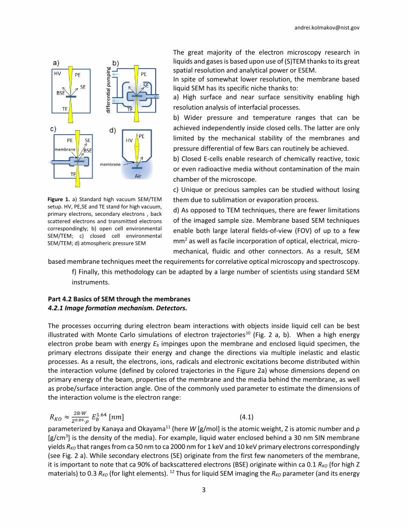
andreikolmakovnistgov
8
liquid cell microscopy but does not necessarily leads to optimal imaging since electron scattering cross section becomes reduced with energy and small nanoparticles even being close to the membrane would not have enough material to provide a measurable BSE signal Part 43 Few examples of environmental cell designs and liquid SEM applications
Recent progress in liquid electron microscopy is a direct result of success in high yield microfabrication technology of ultrathin membranes developed for MEMS devices ultrafiltration and X-rays (electron) transparent windows and development of commercial available tools for research application A number of vendors offer an array of Si SiO2 Si3N4 (SiN) SiC polyimide and other membranes with the thickness ranging from 5 nm to 200 nm which can be used for assembling custom made liquid cells To date the majority of the liquid cell SEM results have been obtained using Quantomix wet cells though alternative commercial membrane based liquid cells have become available recently13
14 In this section we describe the commercially available QunatomiX wet cells and related research that extends this instrumentation to new applications
431 QuantomiX WETSEM capsule design The development of the WETSEM technology by QuantomiX15 in early 2000s was a response to growing demand for in vivo imaging of biological tissues and live cells with spatial resolution better compared to conventional light microscopy Detailed designs capabilities and applications of this approach can be found in the literature5 15 16 The cell principal design is depicted in the Fig 5 and it consists of two parts the top sample dish with electron transparent membrane covering the sample compartment and the stub The cell can be vacuum sealed with a rubber membrane used to joining the two elements The sample compartment can be filled with ca 15 microL of liquid sample Several modifications to the conventional cell body design were proposed15 Proposed modifications include insertion of fiber optics for correlative SEM and cathodoluminescence imaging of hydrated samples16 (see Figure 5 b-d) The QuantomiX WETSEM is enabled with a robust 145 nm thick polyimide electron transparent membrane supported by metal grid The grid provides sufficient mechanical stability for the membrane to withstand atmospheric pressure
Figure 5 a) The basics of QuantomiX WETSEM capsule design b) The realization of the complementary SEM and optical imaging in WETSEM capsule via introduction of an optical fiber c) BSE image of the fully hydrated untreated CHO cells visualized simultaneously with cathode luminescence (CL) signal (d) (Adapted from S Thiberge etal PNAS 2004 101 3346-3351 Copyright (2004) National Academy of Sciences USA
andreikolmakovnistgov
9
differential and yet offers a large segmented ca 4 mm2 FOV The rubber membrane that separates the two elements of the liquid cell is a thin elastomer material that expands in vacuum and functions as a pressure relief element that reduces the risk of polyimide membrane rupture during cell closing and SEM vacuum pumping
The 145 nm thickness of the polyimide membrane implies usage of BSE with energies in excess of 10 keV for SEM imaging of wet samples (see Figure 3) Due to strong attenuation of the BSE signal by the membrane and interfacial water layers it is crucial requirement to have a sample in a close proximity or adhered to the inner surface of the membrane Thus a number of protocols that functionalize the membrane surface to promote nanoparticles adhesion as well as cells culture growth have been developed To work with wet biological tissue biopsies plants sections and other soft samples an upgraded capsule was designed15 The latter was equipped with the special spring loaded piston which gently pushes the tissue against the membrane
432 Applications examples
4321 Water remediation
Numerous studies in variety of fields have been performed using QuantomiX cells17-23 The selection of
research described in the Fig 6 demonstrates use of the wet SEM cells for in situ observation of the metal
remediation in water by TiO2 based photo catalysis24 Electron-hole pairs generated in catalysis particles
by the UV radiation from the Sun can diffuse to the surface and reduceoxidize ionic and molecular
pollutants in water such as heavy metal ions25 An example of such a photo catalytic reaction is UV photon
induced reduction of ionic Ag to metallic nanoparticles at the surface of BaTiO3 catalysis in AgNO3 water
Figure 6 a) SEM image of as prepared bare BaTiO3 photocatalyst b) similar micro particle after UV light exposure in 10-4 M
aqueous solution of AgNO3 Ag reduction can be seen on (001) facet (Adapted from ref [26]) c)-f) In situ reordered
sequential liquid SEM images of a titania whisker immersed in 10-4 M aqueous solution of AgNO3 Areas marked with circles
triangles and squares show divergent growth morphologies as a result of electron beam induced reduction of Ag ions
Imaging conditions 30kV acceleration voltage and BSE detector g) The mechanism of electron beam induced reduction of
Ag ions at the surface of TiO2 h) blue curve corresponds to EDS spectra recorded from AgNO3 solution and red from Ag
decorated TiO3nanowire Adapted with permission from N Kolmakova and AKolmakov J Phys Chem C 2010 114 (40) pp
17233ndash17237 Copyright (2010) American Chemical Society
andreikolmakovnistgov
10
solution26 Fig 6 a b demonstrates an ex
situ SEM comparison of BaTiO3 photo
catalyst before and after illumination with
UV light Since BaTiO3 is ferroelectric it has
a spontaneous polarization which affects
the chemical reactivity of different crystal
facets As can be seen in the Fig 6b Ag
becomes deposited only on (100) facet
implying that the internal polarization
promotes the photo catalytic action to
occur predominantly at this interface26
Observation of such a process in situ is
possible using QuantomiX WETCELL
instrumentation In this case TiO2 single
crystal whiskers are adhered to the liquid
cell inner membrane and in either a pure
water or ca 10 microL of 10-4 M AgNO3 aqueous
solution was dropped into the E-cell
compartment No changes occur in
morphology and shape of the titania
nanostructure as a result of exposure to a
30 keV electron beam in pure water
Conversely imaging TiO2 single crystal
whiskers in an AgNO3 solution shows the
TiO2 nanostructure becoming progressively
decorated with metal particles as depicted in Fig 6 c-f The origin of this phenomenon is similar to photo
catalysis and is due to electron induced reduction of the Ag ions from the solution at the surface of the
TiO2nanostructure The difference between these two experiments is that electronndashhole pairs are created
in TiO2 by the primary electron beam in the liquid cell system Assuming that the stoichiometry of the
electron induced reaction taking place at the surface of TiO2 nanowire submerged in AgNO3 solution is
analogous to the classical photocatalytic reaction (photoreduction) 27 one can write
2 0
2 24 2 4 4TiO
e beamAg H O Ag O H
(410)
where the first frac12 reaction is a transfer of an excited electron to the Ag+ bound to the TiO2 surface leading to the growth of Ag0 domains with high quantum yield The hole transfer to the surface-bound water or hydroxyl groups completes the second frac12 reaction The diagram of the electron induced silver deposition process is depicted in the Fig 6g Evolution of the EDS spectra before (blue curve) and after (red) nanoparticle particle growth demonstrate the accumulation of Ag depositions on the nanowire and the feasibility of recording of EDS spectra on objects in liquid cells
4322 Phytotoxicity The growing production of nano-enabled materials such as engineered nanoparticles (ENP) raises
concerns regarding waste byproduct and potentially negative ENP impacts on human health and
Figure 7 a) The anatomy of Arabidopsis root tip (b c) laser scanning confocal microscopy of Arabidopsis root tip exposed to 270 microgL of 40 nm Ag NPs for 4 weeks panels b) and c) represent the surface (8 microm below the root surface) and semi-median (ca 36 microm below the root surface) scans correspondingly showing distribution of AgNPs in larger root cap cells epidermis and columella initials d) NP decorated Arabidopsis roots imaged with SEM in water e) Higher resolution SEM images of fully hydrated Arabidopsis root cup cells with visible interior (nucleolus) and Ag nanoparticles decorating cellular walls Adapted from ref [29]
andreikolmakovnistgov
11
ecosystems Plants are direct or indirectly consumed element in the human food chain motivating the investigation of the uptake and accumulation of ENP by plant roots and leafs Therefore an application of liquid SEM is ENP phytotoxicity on living plants We test the capabilities and limitations of this imaging modality to probe the in vivo uptake and accumulation of nanoparticles and metal ions by plants at the cellular level A recent example of such an approach is a study of cellular accumulation and subcellular transport of Ag nanoparticles in Arabidopsis thaliana28 Arabidopsis root anatomy is well understood (Figure 7a) and is often used as a model pant system In this experiment a diluted Ag nanoparticles-water colloid was added to a hydroponic nutrient solution (Hoagland solution) where seeds of Arabidopsis thaliana where germinated and different sizes and concentrations of Ag ENPs were tested After controlled growth and uptake the tips of the plant roots were sectioned in a wet state and adhered to the back side of the electron transparent membrane of the QuantomiX WETSEM and cell was filled with water Figs 7 b c shows two laser scanning confocal microscopy optical sections of the root tip exposed to 40 nm Ag ENP and recorded at near surface and at the median part of the root correspondingly Correlative liquid cell SEM images are depicted in the Figs 7 d e Significantly improved resolving power and signal to noise (SNR) ratio from the WETSEM instrumentation reveal that after two week of roots exposure to ENP the accumulation predominantly takes place at root cap at columella cells and border cells28 At low concentrations and exposure times the cell walls of those are coated with individual nanoparticles at surface densities sufficient to impede incoming solute transport The detailed SEM image analysis of the intercellular regions (supported with ex situ TEM studies) indicated the presence of Ag NPs aggregation at plasmodesmata connecting adjacent cells Ag ENP aggregation at plasmodesmata may lead to blockade of the symplastic transport between cells and thus degrade system viability
4323 High radiation dose effects In spite of the demonstrated advantages of liquid cell SEM for high resolution analysis of ENP fate
in plants limitations exist for application of this technique to biological objects Inelastic interaction of the probe beam with liquid water and biological material results in the generation of a variety of ionized and excited molecular species in the interaction volume (see chapters 7 9 and references therein29 ) As a result steady state concentrations of strongly reducing and oxidizing species such as hydrated electrons (eh
minus) hydroxyl radicals (OHbull) hydrogen peroxide H2O2 hydrogen radicals (Hbull) H3O+ as well as molecular hydrogen and oxygen (H2 O2) are formed in and around the interaction volume Assuming that that the radiation dose rate in standard SEM measurements is somewhat larger (ca 108 to 109 Gys) compared to
Figure 8 a) Liquid SEM image of Arabidopsis thaliana with cellular walls decorated with 60 nm Ag nanoparticles b) c)
Electron beam induced Ag nanoparticles dissolution and plant tissue degradation in water with growing radiation dose d)
Two order of magnitude increase of the beam intensity at specified locations reverses the process and results in Ag0
redeposition on membrane inner surface
andreikolmakovnistgov
12
TEM case (ca 108 Gys) and following the scaling laws deduced in ref 29 one can expect the steady state molar concentrations of OHbull and H2O2 species to be in excess of 10-4M The radiolysis byproducts from probe beam illumination contribute significantly to chemical stability of nanoscopic objects in solution and degradation of biological samples An example of the probe beam induced degradation of fully hydrated biological tissue is shown in the Fig 8 Here panels a b and c show a selection of sequential liquid SEM images of the root cup of Arabidopsis thaliana immersed in water following incubation in Ag ENP Similar to Fig 7 nanoparticles accumulate at root cup cell walls and are immobilized Significant degradation of the cell walls can be observed following low dose SEM imaging (ie 10 enm2) while continued exposure leads to complete decay of the cell walls (Fig 8 c) evidenced by reduced image contrast as well as release and dissolution of decorating 60 nm Ag nanoparticles
Noticeably increasing the dose by two orders of magnitude for the same solution by increasing scanned probe beam dwell times results in aggregation of Ag on to the back side of the membrane (Fig 8 d) This interplay between ENP dissolution and growth phenomena as function of electron dose rate can be explained by the radiolysis conditions driven by the incident probe beam Local redox reactions with participation of metal ions are controlled by relative concentrations of primary reducing (eh
minus) and oxidizing (OHbull) agents (see chapter 7 of this book) The relative concentration of solvated electrons increases with incident probe beam electron dose driving reduction of Ag+ + eh
minus Ag0 and growth of Ag depositions At lower beam intensities the opposite process occurs where metal dissolution prevails The probe beam dose borderline between deposition and dissolution was determined to be between 10-9 and 10-10 Gys for TEM experiments a value close to SEM dose imaging conditions
These recent findings will help better control of the probe beam induced nucleation and growth processes in liquids as well as promote the development of SEM electron beam induced deposition (EBID) process in liquids reviewed in Chapter 1430 Coupled with electrochemistry the latter process will have drastically increased selectivity and deposition yield compared to its vacuum analog Furthermore a much greater moiety of chemical and bio species can be used for EBID in liquids Flushing of gas or liquid media inside E-cell can be easily done without braking SEM vacuum enabling nanoscopic sequential deposition of different chemical species in the system
433 Prospective upgrades of QuntomiX WETSEM capsules
andreikolmakovnistgov
13
Currently the QuantomiX WETSEM capsules are mainly used by the bio-medical research
community and the usage of these E-cells for materials research is limited Adoption of this instrumentation by the materials community is restricted by the limited capabilities of these capsules to vary the temperature of the imaged sample as well as altering in situ its chemical and electrical (electrochemical) environment Development of these capabilities would broaden the utility of WETSEM systems for martial science application Our Initial efforts to develop these instrumentation capabilities is depicted in the schematics of Fig 9 where central stub of QuantomiX QX-302 capsule has been modified to be used for connection of multiple electrical leads and tubing for gas or fluid delivery Use or removal of the metal coating of the standard capsule stub assembly enables control of electrical connections to the capsule and fluid solution while vacuum sealing of electrical leads and fluidic tubing is enabled by application of UV curable glue
Thermal control over the sample environment was enabled through development of a simple heating and cooling system based upon a miniature 4 W Peltier element and copper heat sink (Fig 9a)31 In this system the heat from the thermoelectric module is delivered to the electron transparent membrane using a copper bar connecting the membrane supporting metal grid of the capsule to the thermoelectric module The bar is spring loaded against the membrane supporting mesh and maintains thermal contact with the grid while enabling capsule assembly and disassembly Using this setup temperatures as low as -10 degC and as high as 100 degC can be achieved at the membrane (Fig 9b) The use of more powerful thermoelectric elements enables a larger range of system temperatures
The ability to cool or to heat samples in their native gaseous or liquid environments at a variety of pressures opens new possibilities in SEM which cannot be achieved using commercially available cryo- or heating stages For example the particularities of water condensation wetting and flow in 3D photonic structures enable understanding the fundamental processes controlling optofluidics32 33 and sensorics34
Figure 9 a) Customization of QuantomiX capsule with addition of heatingcooling electrical and fluidic capabilities
b) Temperature of the sample supporting membrane in (a) as a function of power of the 4W thermoelectric element
c) consequent liquid SEM images of water condensation at Morpho butterflies scale upon cooling inside water vapor
filled QuantomiX capsule (see details in the text and in ref [32])
andreikolmakovnistgov
14
Fig 9 c shows mesoscopic details of initial stages of water condensation at the surface of natural photonic structure butterfly wings The butterfly scales were adhered to the back side of electron transparent membrane which can be heated or cooled inside the QuantomiX capsule The capsule contained the water droplet separated from the membrane thus dew can be formed or evaporated via cooling or heating the membrane loaded with butterfly scales Panel 1 of Fig 9 c shows a SEM image of the characteristic mesoscopic ridge structures of a stacked periodic layers of cuticle separated by the air gaps of a dry Morpho butterflies scale For comparison panels 2 and 3 of Fig 9 show sequential images of the same region upon cooling in the presence of water vapor In this figure water first condenses at the top of the ridges after which the condensation front spreads along the ridges As recently discovered this particular condensation pattern is due to existing gradient of surface polarity along the height of the ridge from the polar ridge tops to the non-polar bottoms35 The water therefore preferably condenses and spreads along the top part of the ridges leaving air pockets deeper inside the scales resulting in a hydrophobic wing structure that allows the butterfly to shed water droplets Note that the improved lateral resolution of this process is achieved using conventional ESEM vs a liquid cell system However the former approach does not allow decoupling of thermal and pressure induced processes and has limited pressure range
434 Example of a custom design of the E-cells for electrochemical studies in liquids Increased functionality of the environmental cells used for electron microscopy is a current trend
in TEM and STEM studies Several types of fluidic heating and electrochemical cells have become available recently36 37 And many of the commercially available or custom developed E-cells for (S)TEM can be directly adapted to SEM research as well14 38 The latter approach however is rarely adopted by SEM community since the core advantage of the SEM large field of view fast exchange and analysis of arbitrary samples cannot be easily implemented in thin TEM flow cells with characteristic submicron fluidic flow channels As a result several custom made E-cells specifically designed for complex SEM studies have been reported39-41 One of these simple and cost effective instruments is described below
Recent energy and environmental initiatives resulted in growing application of SEM in liquids and dense gases including research into morphological and compositional alterations of nanoscopic devices
andreikolmakovnistgov
15
and interfaces during operation in realistic environmental conditions In many research settings there often require variety of objects within the imaged FOV for comparative or combinatorial analysis The latter experiment requires development of the complex circuitry on electron transparent membrane and parallel indexing of multiple electrodes A practical solution to this experimental challenge is to employ SiN membrane widows on SiNSi chip with lithographically defined electrodes array Such an electronic chip-with-a window can be wire bonded to standard vacuum compatible ceramic chip carrier (Figure 10 ab ) requiring only slight modification such as a millimeter size hole through the center of the device39 For electrochemical studies the surface of the electrical leads and other metal surfaces are coated with SiO2 insulating layer as shown in Fig 10 b The assembly can be used in two different setups For
correlative optical and electron microscopy the 70 L cavity was filled with a 1 mM solution of AgNO3 to act as a model electrolyte and covered with a glass lid sealed to the device with UV curable adhesive The glass lid acts as a viewing port making the cell usable with both optical and SEM thus enabling correlative microscopy analysis Alternatively the fluidic chamber can be attached to the chip carrier (Figure 10 c d) to enable exchange of the solution within the device Fig 10 e shows a cyclic voltammogram of Ag plating (stripping) from AgNO3 water solution on to (from) SnO2 nanowire wired as a working electrode The
Figure 10 Design and results of multi-electrode electrochemical cell that enables in situ electrochemical studies in
liquid using SEM and optical microscopy a) standard ceramic chip carrier equipped with electron transparent SiN
window b) the electron transparent window with multiple electrodes for electrochemical SEM studies in liquid
electrolytes c) and d) the picture and design of the corresponding fluidic cell e) the voltammogram of Ag plating
and stripping atfrom SnO2 whisker immersed in 10-3 M AgNO3 solution with corresponding liquid SEM images
Adapted from ref [39]
andreikolmakovnistgov
16
corresponding in situ liquid SEM images demonstrate the morphology of Ag0 deposit from the solution as well as it complete stripping at a reverse potential An in-situ comparative energy dispersive X-ray (EDS) analysis has been recorded (not shown here) before and after the deposition of Ag supporting the deposition of pure silver on to the surface of the SnO2 nanowire
Part 44 Novel 2D materials as electron transparent membranes for liquid SEM cells 441 Why do we need them In spite of great progress in implementation of SiN SiO2 and polyimide membranes in liquid SEM (STEM) cells reduction of beam scattering and signal attenuation by the membrane itself would improve SEM image quality analytical capability and reduce electron dose into the sample The strategy to improve the scattering and transparency of the membranes are based upon the reduction of their thickness and atomic Z number of the membrane materials Commercially available SiN and SiO2 -based membranes fabricated via SiN (SiO2)Si wafer back KOH etching process are as thin as 5 nm However due to fluctuations in Si etching speed such membranes can be produced reliably with minimal windows sizes of ca 10 microns or larger With large effective diameters such thin windows are prone to mechanical collapse under the one atmosphere pressure differential in vacuum systems and are thus not ideal for liquid SEM E-cells Prospective technological approaches based upon fabrication of large-area perforated-supporting membranes with micron size orifices enable much thinner membranes Such electron transparent windows are the base of modern E-chips of ambient pressure TEM and can in principle be adapted for ambient pressure SEM studies
andreikolmakovnistgov
17
An alternative approach to reducing atomic number and membrane thickness includes novel free standing membranes42 43 made of single atomic layer two dimensional (2D) materials such as graphene graphene oxide and etc These membranes are impermeable to liquids and gasses and enable new capabilities for TEM and SEM in liquids The two major differences with respect to standard SiN or SiO2 membranes are that graphene based membranes have extremely high breaking strength44 that facilitates fabrication of atomically thin electron transparent windows such that inelastic electron mean free path
lengths in single layer graphene for an example are larger than its thickness at SEM range electron acceleration voltages We infer from this property that incoming and outgoing electrons can pass such a membrane without significant attenuation Opportunities are even more intriguing for very low energy electrons ( lt5 eV)45 For such electrons the electron-electron scattering is further hampered and electron ndash phonon scattering is inefficient Therefore for low energy secondary electrons these membranes can be nearly totally transparent Thicker multilayer membranes (eg 1 to 2 nm) have higher strength and more robust performance These membranes are thus practical for liquid SEM measurements As a result of these properties new opportunities for SEM emerge a) True SEs can be used for imaging the surfaces of objects covered with such a membrane Therefore data can be acquired from specimens at ambient pressure in fully hydrated conditions with SEM resolution and surface sensitivity b) An array of powerful surface sensitive analytical techniques such as XPS AES NEXAFS etc can be applied to such objects Additional advantages include c) Smaller primary beam energies can be used enabling smaller excitation volumes and reduced beam induced damage d) Negligible charging effects due to fast neutralization of the accumulated charge ether by conducting electrons (in G GO) or in case of dielectric membranes (eg BN) via tunneling from
the conducting liquid media e) Longer stability of the graphene membrane with respect to knock-on process since SEM electron beam energy is well below the energy threshold for graphene (~80 keV)46
The electron transparency of the 2D free standing graphene boron nitride or graphene oxide membranes or coatings was evaluated in multiple reports using TEM 43 47 48 for high energy electrons as well as point projection microscopy49 50 and SEM51 for slow ones Complementing surface science studies the electron attenuation length (EAL) parameter was used as an equivalent to inelastic mean free path assuming that elastic scattering is negligible as signal returns to the detector 52 EAL relates the initial
electron flux of secondary and back scattered electrons (I0) from objects under the membrane to the one
(I) measured by the detector
Figure 11 Experimental data points (filled circles)
represent the effective attenuation length (EAL) for
graphene monolayer from ref [56] and from ref [57]
(diamonds) In addition EAL data (diamonds) For
comparison horizontal dashed lines denote the
thicknesses of single and bilayer graphene Solid
line predicted inelastic mean free path in graphite
as calculated using TPP-2M formula [54] Adapted
from ref [56]
andreikolmakovnistgov
18
119868 1198680 = exp(minus(119871
120582119872+frasl
119889
120582119866)) (411)
here λG λM are EALs for graphene membrane and the media between the object and the membrane while d and L stand to thickness of corresponding layers as shown in the inset of Fig 11) This method is widely used to determine the thickness of overlayers for materials with known EALs53 Using this calculation EALs for graphene and graphene oxide were measured via collecting the substratersquos XPS54
55 AES56 and secondary electrons57 signals attenuated by the known amount of graphene or GO layers Fig 11 compiles some of this experimental data and compares them with theoretical predictions for carbon53 The reasonable agreement can be observed for the electrons acceleration voltages exceeding 70 eV EALs for energy ranges below this value have yet to be explored
442 Preparation of the graphene and graphene oxide membranes Graphene oxide (GO) was the first 2D material tested as an electron transparent window for SEM
E-cells54 58 The attractiveness of GO membranes stems from the well-developed high-yield GO production protocols of this material as discussed by Park and Rouff 59 and references therein Conveniently chemically exfoliated GO flakes have hydrophilic edges due to terminating COOH groups and hydrophobic basal plane due to the presence of domains of intact graphene Being amphiphilic GO flakes in water solutions segregate at air-water and water-solid interfaces to form membranes60 61 thus enabling Langmuir-Bludget or simple drop casting methods to be applied to fabricate suspended membrane When dried such membranes (often called GO-paper when thicker than few microns) have excellent 100 MPa 62 tensile strength that can be further enhanced by GO functionalization with divalent ions like Mg2+ and Ca2+63
Many different approaches to fabricate GO suspended membranes have been reported43 54 58 64 We have used diluted GO water or methanol solutions to cover micron wide orifices with a single flake of GO using LangmuirndashBlodgett deposition method54 This procedure can be repeated multiple times to fabricate multi-layer membranes Such membranes are molecular impermeable and mechanically sable under pressure differential if their diameter is below 3-5 microns Larger and therefore thicker membranes can be easily fabricated simply by drying of the GO solution over the small orifices58 Alternatively GO solution can be dried on the support which than can be suspended with a selective backside chemical or electrochemical etch58 64
As shown in recent reports64-66 GO membranes made of interlocked flakes have selective permeation properties that favor the capillary uptake and diffusion of water between stacked GO flakes GO permeation property results from GO flake separation distance d which is between 7Aring and 11 Aring depending on degree of GO reduction The flake separation distance is sufficient to accommodate one to two layers of water Interestingly such GO membranes are vacuum tight for many other gases and liquids such as atmospheric gases and alcohols64 This property makes GO excellent prospective material for selective filtering of media but a poor system for liquid water SEM experimental research To perform liquid SEM studies with GO membranes one can adopt several strategies (i) completely cover the orifice with an individual single layer or multilayer GO flake using the Lanmuir-Bludget approach (ii) adopt thicker GO membranes covering larger orifices that have less than one percolation channel inside the orifice The latter approach can be achieved by accounting for total length l and surface density s of the percolation
channels in GO membrane of thickness h scaling as 119897~ ℎ119871119889frasl and L-2 correspondingly where L is the average
size of the GO flake64 Thus the number N of the water conducting channels in an orifice of size D is
119873~(119863119871frasl )
2 Assuming the average size L of the GO flake in solution ~ 10 microns fabrication of GO water
impermeable multilayered electron transparent membranes can be done providing the size of the orifice D does not exceed L~10 microns58 Furthermore mildly annealed GO in the range between 120 and 150
andreikolmakovnistgov
19
degC eliminates the percolation water layers reducing d of the membrane without causing irreversible thermal reduction
Graphene on the other hand can be fabricated as a single layer carbon sheet and therefore is a nearly ideal material for e-cells since it is low atomic number has a small scattering cross section chemically inert ultrathin mechanically robust and lacks the aforementioned GO drawbacks The bulge and indentation tests demonstrated that suspended membranes are gas impermeable and yet have unprecedented robustness with stiffness in excess of 1 TPa67 what allows to sustain pressure differential of few Bars with diameters of the window below ca 5 microm
High quality large scale single and multi-layer graphene is routinely grown by CVD on Cu or Ni substrate and can be easily transferred to the substrate of interest by chemical etching of the substrate and via using PMMA film as sacrificial supporting layers Many other wet and dry transfer protocols were developed in recent years (see reviews 68 69 and references therein) As in the case of GO graphene membrane can be transferred on to the micron size apertures made by FiB micro pattering or laser drilling in the SiN SiO2 or metal supporting frame Graphene transfer processes involve removal of the interfacial liquid layer and residual contaminants from the graphene growth and release protocol This can be best done via slow annealing either in vacuum or under reducing (ArH2 mixture) ambient (see protocols in70) The annealing process also improves adhesion of Graphene to the substrate 443 Graphene and GO based E-cell design Two different graphene based closed cell designs have been tested as shown in Fig 12 The single use Si
based cell consisted of SiN primary membrane with FIB drilled micro-orifice LB covered with one or more graphene or GO layers The chip was filled with liquid sample and placed on a supporting Si plate (Fig 12a) Two part device are sealed with UV curable glueA silver paste patch is used to make a conductive ground for the device The principle design of the liquid cell with exchangeable graphene or GO windows is depicted in Fig 12 b The core of this E-
cell is a metal plate or SiNSi membrane with a laser or focused ion beam drilled hole for an aperture The standard PMMA based graphene transfer protocol was used to cover these 1-3 micron orifices Following deposition of graphene on the surface the system was annealed in air and PMMA was dissolved using warm acetone71 In the case of GO membranes the aforementioned Langmuir-Blodgett or drop casting protocols can be used to construct a membrane An exchangeable disk with a droplet of liquid sample is placed between two metal plates and vacuum sealed using pressure relief rubber membrane gasket The design of the cell allows isolation of a ca 20 μL sample and reduction of the pressure differential on to the graphene (GO) membrane when the liquid contains an excess of trapped gas and in vacuum
Figure 12 Principle design of closed graphenegraphene oxide E-cell a) single use cell b) refillable cell with exchangeable graphene (GO) membranes Adapted from refs [55] (a) and with permission from M Krueger et al ACS Nano 2011 5 10047-10054 Copyright (2011) American Chemical Society (b)
andreikolmakovnistgov
20
444 SEM imaging with GO and Graphene membranes The performance of the GO liquid cell filled with 50 nm Au colloid water solution can be evaluated
from the images in the Figure 13 a b Both images were obtained under the same SEM settings but using different detectors backscattered electrons detector (BSED Fig 13 panel (a)) and Everhart-Thornley detector (ETD Fig 13 panel (b)) which have larger and lower probing depth correspondingly Since ETD is sensitive to low energy secondary electrons greater detail of the membrane surface morphology (such as multiple GO wrinkles) can be seen The profile analysis of the gray scale values of the individual 50 nm Au
nanoparticles adhered to the back side of the ca 30 nm thick GO membrane (Figure 13 c) indicates that electron scattering in this low Z membrane does not deteriorate the resolution of the NP image significantly In addition to imaging EDX analysis can routinely be performed on a particles through the membrane as shown in the Fig 13 d
The examination of the gray scale variations taken with the ET detector as a function of the beam energy (not shown here) reveals the possibility for imaging high Z Au nanoparticles through the GO membrane using very low electron beam energies (starting from 1 keV) Since the thickness of the membrane (ca 30 nm) is an order of magnitude larger compared to inelastic mean free path for secondary electrons in GO54 detected electrons are backscattered and related secondary electrons of type S2 and S3 that compose SEM signal12
445 Radiation and
chemical stability of the graphene based membranes
Electron beam induced water radiolysis and radical generation is a significant effect in liquid electron microscopy and usually discussed in terms of impact on to the imaged objects Different from thick SiN membranes the direct defect formation or indirect beam induced chemical damage to thin 2D membranes are important issues in liquid SEM measurements since membrane damage limits the life time of the electron transparent windows of E-cells A selection of the available results are discussed below
The direct defect formation in the membranes can be due to electron induced atomic displacement (ldquoknock-onrdquo process) or as a result of relaxation of the electronic excitation inside the membrane The former mechanism has an energy threshold estimated to be 80 keV46 and is predicted to be inefficient at probe acceleration voltage energies used in SEM On the other hand the cross section for the inelastic electron excitation processes increases with lowered electron beam energies and is
Figure 13 a) SEM image of the Au NP solution through ca 40 nm thick GO membrane Image conditions beam energy 30 keV detector BSE tilt 39deg b) SEM taken under the same conditions but using Everhart-Thornley detector The scale bar corresponds to 5 microm c) Inset high resolution SEM image of two 50 nm Au nanoparticles immersed in water and adhered to the back side of the membrane Gray scale value line profile over the individual 50 nm Au nanoparticle d) EDX spectrum taken from Au NP aqueous solution through the GO membrane The red peaks correspond to Au lines and unmarked peaks originate from the surrounding stainless steel frame Adapted with permission from M Krueger et al ACS Nano 2011 5 10047-10054 Copyright (2011) American Chemical Society
andreikolmakovnistgov
21
significant at low keV acceleration voltages This damage mechanism can result in chemical bonds breakage and local heating The thermal conductivity of the graphene at room temperature is high (ca 5000 WmmiddotK)72 and no noticeable damage due to electron beam heating effect is expected This damage mechanism is even less probable when gaseous or liquid media is in contact with 2D membrane
For practical SEM imaging through 2D membranes it is important to know these threshold doses of noticeable electron induced defect formation and to minimize all aforementioned effects via reducing the electron beam exposure Beam exposure effects is difficult to define as there is significant variation in published experimental data experimental conditions and often dose measurements are not recorded in SEM experiments This issue is further complicated by a variety of energy dissipation mechanisms during e-beam irradiation of hydrated samples GO membranes were found to be prone for photo-thermal reduction with a flash light 73 74 and laser light illumination A characteristic threshold was measured to be ca 102 mJ cm2 for a micron thick GO membrane73 corresponding to an electron beam dose of ca 1 enm2 for 10 keV electrons assuming full absorption of probe beam energy by the film Alternative results indicate that GO films did not suffer reduction from a 20 keV electron probe beam until reaching doses as high as 103 enm2
75 Data is also available for electron beam induced damage of graphene layers from SEM
imaging and electron beam lithography It has been observed for graphene field effect transistors (GFETs) that the appearance and growth of the disorder D peak in Raman spectrum of the supported graphene as well as concomitant increase of its resistivity (mobility drop) occur after irradiation with doses as low as 20 enm2 76 Bi-layer graphene was found to be significantly more stable to radiation damage Similar measurements on the suspended graphene FET demonstrated considerably smaller change of the electronic properties upon even larger (102 enm2) irradiation doses while the growth of the DG Raman peaks ratio remained nearly the same as in the case of supported graphene77 The latter observation implies that the observed changes in Raman signatures or electron mobility can be due to beam induced modification (eg local charging) of the supporting substrate or electron beam induced carbonization of the graphene layer 78 but not due to massive defect formation in the graphene itself
The presence of the dense gaseous or liquid media in contact with graphene (or GO) can catalyze the formation of new or develop pre-existing defects indirectly via generation of ionic or radical species that attack 2D membrane chemically As it has been shown recently in STM studies of water exposed to graphene this is particularly relevant to linear defects and grain boundaries in this material79 Another example is reduction of the GO by electron beam generation of plasmas produced in inert (Ar) reducing gases (CH4) or their mixtures80 Similar processes occur in water during beam induced water radiolysis which has been extensively studied (eg ref 81 and references therein) Chemically reactive products such as molecular hydrogen (H2) hydrogen peroxide (H2O2) and hydroxyl radicals (OH) produced in water by radiolysis can accumulate 81 and reduce or oxidize the 2D membrane weakening or dissociating C-C bonds at defects sites In addition under prolonged exposure volatile products of radiolysis can eventually segregate as a separate phase forming microbubble under 2D membrane potentially leading to a pressure buildup inside the E-cell and capillary induced collapse of the membrane We estimated that 20 keV electron beam irradiation of liquid water under the graphene membrane leads to bubble formation following accumulation of critical dose of ~104 enm2 55 82 SEM operation below bubble forming dose levels enables good image acquisition conditions as data maybe be acquired at dose levels of (~102 enm2) from illumination areas ca ~102 microm2 This problem can be further reduced in fluidic cells where replenishable solution is used thus enabling removal of radiolysis byproduct from the probe beam scan area
Outlook Nanoscale imaging in liquids and at solid- gas -liquid interfaces enables research in the fields of materials science biomedical forensics chemistry and environmental research We expect membrane based liquid scanning electron microscopy be a growing field of research in years to come Based on the current trends
andreikolmakovnistgov
22
one can envision three different lines of near future activities and developments of this microscopy modality
1 Theory modelling and fundamental research on chemistry and physical aspects of the electron beam interaction with liquid matter and immersed objects This research includes the understanding of beam induced local chemistry in liquids and dense gases spatial and temporal distributions of reactive species and their possible influence on the immersed objects The probing of the different systems such as operational electrochemical and fuel cells as well as living biological objects will continue along with the efforts to minimize beam induced artifacts via improving the sensitivity of the detectors and implementation of modern image processing and data mining algorithms There is also clear trend to combine different imaging modalities
2 Liquid cells designs The electron transparent windows with the thickness of 20-50 nm based on modern SiN SiO2 or SiC microfabrication processes will be a dominating technological platform for near future liquid SEM The variety of experimental tasks and objects makes it almost impossible to create a universal liquid SEM cell therefore similar to modern liquid TEM trends some degree of specialization in the cell will take place For example fabrication of SiN electron transparent windows dedicated to electrochemical variable temperature studies in situ
micromanipulation and electrical measurements can be envisioned The overall design of the future liquid cells will be single use monolithic chip with so-called on board fluidics where the source liquids and electrophoretic electroosmotic or micromechanical pumps are integral parts of the lab-on-chip liquid SEM technology 3 Membranes development Novel 2D materials with ultimately high electron transparency and mechanical strength will remain the object of active research and technical developments The driving force behind this line of the research is the unique capability to use powerful surface characterization techniques for liquid interfaces such as XPS55 The combination of the requirement to have large FOV with micron size graphene covered orifices will result in implementation of a new environmental cell platform where the membrane is composed of multiple orifices One of the possible designs of
the graphene based liquid cell is proposed in the Fig 14 The core of the cell is multichannel or microporous matrix which contains high density isolated or interconnected microfluidic channels The channels have openings which are covered with graphene membrane Such a cell can be equipped with heaters and electrodes as well channels can be impregnated with different liquids (A-D Figure 14) Such a design is favorable for the combinatorial SEM studies with correlative electron (eg XPS AES) or optical (cathodoluminescence (CL) IR Vis) spectroscopies Disclaimer Certain commercial equipment instruments or materials are identified in this paper in order to demonstrate the experimental procedures and capabilities adequately Such identification is not intended to imply recommendation or endorsement by the National Institute of Standards and Technology nor is it intended to imply that the materials or equipment identified are necessarily the best available for the purpose
Figure 14 Prospective design of the microchannel sample
platform for liquid SEM through the array of the graphene
covered micro-orifices Adapted from ref[55]
andreikolmakovnistgov
23
Disclaimer Official contribution of the National Institute of Standards and Technology not subject to copyright in the United States Acknowledgements AK thanks his SIUC students Shannon Berg Mark Krueger Joshua Cothren Joshua Stoll and Alexander Yulaev whose work became the base of this chapter The technical discussions with Christopher Brown Alex Liddle Dr Renu Sharma and Nikolai Zhitentev (all at NIST) are greatly appreciated References 1 G D Danilatos Inst Phys Conf Ser 1990 455-458 2 G D Dantilatos US Patent 4596928 1986 3 A Bogner G Thollet D Basset P-H Jouneau and C Gauthier Ultramicroscopy 2005 104 290-
301 4 I Abrams and J McBain Journal of Applied Physics 1944 15 607-609 5 S Thiberge O Zik and E Moses Review of Scientific Instruments 2004 75 2280-2289 6 M Suga H Nishiyama Y Konyuba S Iwamatsu Y Watanabe C Yoshiura T Ueda and C Sato
Ultramicroscopy 2011 111 1650-1658 7 N Vidavsky S Addadi J Mahamid E Shimoni D Ben-Ezra M Shpigel S Weiner and L Addadi
Proceedings of the National Academy of Sciences 2014 111 39-44 8 Y Ominami S Kawanishi T Ushiki and S Ito Microscopy 2014 dfu107 9 E Jensen A Burrows and K Moslashlhave Microscopy and Microanalysis 2014 20 445-451 10 H Demers N Poirier‐Demers A R Couture D Joly M Guilmain N de Jonge and D Drouin
Scanning 2011 33 135-146 11 K Kanaya and S Okayama Journal of Physics D Applied Physics 1972 5 43 12 J Goldstein D Newbury D Joy C Lyman P Echlin E Lifshin L Sawyer and J Michael 2003 13 R Egerton P Li and M Malac Micron 2004 35 399-409 14 D A Fischer D H Alsem B Simon T Prozorov and N Salmon Microscopy and Microanalysis
2013 19 476-477 15 V Behar O Gileadi Y Karni Y Kliger A Nechushtan D Sprinzak and O Zik US patent 7230242
B2 2007 16 S Thiberge A Nechushtan D Sprinzak O Gileadi V Behar O Zik Y Chowers S Michaeli J
Schlessinger and E Moses Proceedings of the National Academy of Sciences of the United States of America 2004 101 3346-3351
17 G Venkiteela and Z H Sun Cement amp Concrete Composites 2010 32 211-218 18 K Tiede S P Tear H David and A B A Boxall Water Research 2009 43 3335-3343 19 B G Mathapa and V N Paunov Physical Chemistry Chemical Physics 2013 15 17903-17914 20 C Lorenz K Tiede S Tear A Boxall N von Goetz and K Hungerbuhler International Journal of
Occupational and Environmental Health 2010 16 406-428 21 D C Joy and C S Joy Journal of Microscopy-Oxford 2006 221 84-88 22 A K F Dyab and V N Paunov Soft Matter 2010 6 2613-2615 23 O Cohen R Beery S Levit J Ilany I Schwartz M Shabtai D Anaby D Cohen R Alfici A
Czerniak and A Karasik Thyroid 2006 16 997-1001 24 N Kolmakova and A Kolmakov The Journal of Physical Chemistry C 2010 114 17233-17237 25 C Wei W Y Lin Z Zainal N E Williams K Zhu A P Kruzic R L Smith and K Rajeshwar
Environmental science amp technology 1994 28 934-938 26 J L Giocondi and G S Rohrer Topics in catalysis 2008 49 18-23
andreikolmakovnistgov
24
27 J M Herrmann Catalysis Today 1999 53 115-129 28 J Geisler-Lee Q Wang Y Yao W Zhang M Geisler K Li Y Huang Y Chen A Kolmakov and X
Ma Nanotoxicology 2012 7 323-337 29 N M Schneider M M Norton B J Mendel J M Grogan F M Ross and H H Bau The Journal
of Physical Chemistry C 2014 118 22373-22382 30 E U Donev and J T Hastings Nano letters 2009 9 2715-2718 31 A Al-Asadi J Zhang J Li R A Potyrailo and A Kolmakov arXiv preprint arXiv150100762
2015 32 C Monat P Domachuk and B Eggleton Nature photonics 2007 1 106-114 33 D Erickson D Sinton and D Psaltis Nature Photonics 2011 5 583-590 34 R A Potyrailo H Ghiradella A Vertiatchikh K Dovidenko J R Cournoyer and E Olson Nature
Photonics 2007 1 123-128 35 R A Potyrailo T A Starkey P Vukusic H Ghiradella M Vasudev T Bunning R R Naik Z
Tang M Larsen and T Deng Proceedings of the National Academy of Sciences 2013 110 15567-15572
36 R R Unocic X-G Sun R L Sacci L A Adamczyk D H Alsem S Dai N J Dudney and K L More Microscopy and Microanalysis 2014 20 1029-1037
37 K Klein I Anderson and N De Jonge Journal of microscopy 2011 242 117-123 38 K Moslashlhave C Kallesoslashe C Wen F Ross T Booth T Kjoslashller Nellemann E Jensen C Elkjaeligr J
Rasmussen and P Jensen Microscopy and Microanalysis 2010 16 322-323 39 J E Cothren Thesis Master of Science Southern Illinois University Carbondale 2011 40 Y Liu Master of Science Southern Illinois University at Carbondale 2013 41 S Ueda Y Kobayashi S Koizumi and Y Tsutsumi Microscopy 2014 dfu100 42 J C Meyer A K Geim M Katsnelson K Novoselov T Booth and S Roth Nature 2007 446
60-63 43 N R Wilson P A Pandey R Beanland R J Young I A Kinloch L Gong Z Liu K Suenaga J P
Rourke and S J York ACS nano 2009 3 2547-2556 44 C Lee X Wei J W Kysar and J Hone science 2008 321 385-388 45 I Muumlllerovaacute M Hovorka and L Frank Ultramicroscopy 2012 119 78-81 46 J C Meyer F Eder S Kurasch V Skakalova J Kotakoski H J Park S Roth A Chuvilin S
Eyhusen and G Benner Physical review letters 2012 108 196102 47 J C Meyer C O Girit M Crommie and A Zettl Nature 2008 454 319-322 48 R S Pantelic J C Meyer U Kaiser and H Stahlberg Solid State Communications 2012 152
1375-1382 49 J Mutus L Livadaru J Robinson R Urban M Salomons M Cloutier and R Wolkow New
Journal of Physics 2011 13 063011 50 J-N Longchamp C Escher T Latychevskaia and H-W Fink Ultramicroscopy 2014 51 L Frank E Mikmekovaacute I Muumlllerovaacute and M Lejeune Applied Physics Letters 2015 106 013117 52 A Jablonski and C Powell Journal of Vacuum Science amp Technology A Vacuum Surfaces and
Films 2009 27 253-261 53 S Tanuma C Powell and D Penn Surface and Interface Analysis 2011 43 689-713 54 A Kolmakov D A Dikin L J Cote J X Huang M K Abyaneh M Amati L Gregoratti S
Gunther and M Kiskinova Nature Nanotechnology 2011 6 651-657 55 J Kraus R Reichelt S Guenther L Gregoratti M Amati M Kiskinova A Yulaev I Vlassiokiv
and A Kolmakov Nanoscale 2014 56 M Xu D Fujita J Gao and N Hanagata Acs Nano 2010 4 2937-2945 57 V Kochat A N Pal E Sneha A Sampathkumar A Gairola S Shivashankar S Raghavan and A
Ghosh Journal of Applied Physics 2011 110 014315
andreikolmakovnistgov
25
58 M Krueger S Berg D Stone E Strelcov D A Dikin J Kim L J Cote J X Huang and A Kolmakov Acs Nano 2011 5 10047-10054
59 S Park and R S Ruoff Nature nanotechnology 2009 4 217-224 60 D Li M B Muumlller S Gilje R B Kaner and G G Wallace Nature nanotechnology 2008 3 101-
105 61 L J Cote J Kim V C Tung J Luo F Kim and J Huang Pure and Applied Chemistry 2010 83
95-110 62 D A Dikin S Stankovich E J Zimney R D Piner G H Dommett G Evmenenko S T Nguyen
and R S Ruoff Nature 2007 448 457-460 63 S Park K-S Lee G Bozoklu W Cai S T Nguyen and R S Ruoff ACS nano 2008 2 572-578 64 R Nair H Wu P Jayaram I Grigorieva and A Geim Science 2012 335 442-444 65 H W Kim H W Yoon S-M Yoon B M Yoo B K Ahn Y H Cho H J Shin H Yang U Paik and
S Kwon Science 2013 342 91-95 66 R Joshi P Carbone F Wang V Kravets Y Su I Grigorieva H Wu A Geim and R Nair Science
2014 343 752-754 67 J S Bunch S S Verbridge J S Alden A M van der Zande J M Parpia H G Craighead and P
L McEuen Nano letters 2008 8 2458-2462 68 J Kang D Shin S Bae and B H Hong Nanoscale 2012 4 5527-5537 69 F Bonaccorso A Lombardo T Hasan Z Sun L Colombo and A C Ferrari Materials Today
2012 15 564-589 70 Y-C Lin C-C Lu C-H Yeh C Jin K Suenaga and P-W Chiu Nano letters 2011 12 414-419 71 J W Suk A Kitt C W Magnuson Y Hao S Ahmed J An A K Swan B B Goldberg and R S
Ruoff ACS nano 2011 5 6916-6924 72 A A Balandin S Ghosh W Bao I Calizo D Teweldebrhan F Miao and C N Lau Nano letters
2008 8 902-907 73 L J Cote R Cruz-Silva and J Huang Journal of the American Chemical Society 2009 131
11027-11032 74 S Gilje S Dubin A Badakhshan J Farrar S Danczyk and R B Kaner Advanced Materials 2010
22 419-423 75 P Kumar K Subrahmanyam and C Rao Materials Express 2011 1 252-256 76 G Liu D Teweldebrhan and A A Balandin Nanotechnology IEEE Transactions on 2011 10
865-870 77 I Childres L A Jauregui M Foxe J Tian R Jalilian I Jovanovic and Y P Chen Applied Physics
Letters 2010 97 173109 78 L Tao C Qiu F Yu H Yang M Chen G Wang and L Sun The Journal of Physical Chemistry C
2013 117 10079-10085 79 X Feng S Maier and M Salmeron Journal of the American Chemical Society 2012 134 5662-
5668 80 M Baraket S Walton Z Wei E Lock J Robinson and P Sheehan Carbon 2010 48 3382-3390 81 C Royall B Thiel and A Donald Journal of Microscopy 2001 204 185-195 82 J D Stoll and A Kolmakov Nanotechnology 2012 23
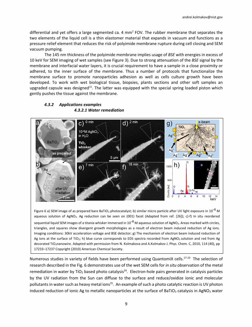
andreikolmakovnistgov
11
ecosystems Plants are direct or indirectly consumed element in the human food chain motivating the investigation of the uptake and accumulation of ENP by plant roots and leafs Therefore an application of liquid SEM is ENP phytotoxicity on living plants We test the capabilities and limitations of this imaging modality to probe the in vivo uptake and accumulation of nanoparticles and metal ions by plants at the cellular level A recent example of such an approach is a study of cellular accumulation and subcellular transport of Ag nanoparticles in Arabidopsis thaliana28 Arabidopsis root anatomy is well understood (Figure 7a) and is often used as a model pant system In this experiment a diluted Ag nanoparticles-water colloid was added to a hydroponic nutrient solution (Hoagland solution) where seeds of Arabidopsis thaliana where germinated and different sizes and concentrations of Ag ENPs were tested After controlled growth and uptake the tips of the plant roots were sectioned in a wet state and adhered to the back side of the electron transparent membrane of the QuantomiX WETSEM and cell was filled with water Figs 7 b c shows two laser scanning confocal microscopy optical sections of the root tip exposed to 40 nm Ag ENP and recorded at near surface and at the median part of the root correspondingly Correlative liquid cell SEM images are depicted in the Figs 7 d e Significantly improved resolving power and signal to noise (SNR) ratio from the WETSEM instrumentation reveal that after two week of roots exposure to ENP the accumulation predominantly takes place at root cap at columella cells and border cells28 At low concentrations and exposure times the cell walls of those are coated with individual nanoparticles at surface densities sufficient to impede incoming solute transport The detailed SEM image analysis of the intercellular regions (supported with ex situ TEM studies) indicated the presence of Ag NPs aggregation at plasmodesmata connecting adjacent cells Ag ENP aggregation at plasmodesmata may lead to blockade of the symplastic transport between cells and thus degrade system viability
4323 High radiation dose effects In spite of the demonstrated advantages of liquid cell SEM for high resolution analysis of ENP fate
in plants limitations exist for application of this technique to biological objects Inelastic interaction of the probe beam with liquid water and biological material results in the generation of a variety of ionized and excited molecular species in the interaction volume (see chapters 7 9 and references therein29 ) As a result steady state concentrations of strongly reducing and oxidizing species such as hydrated electrons (eh
minus) hydroxyl radicals (OHbull) hydrogen peroxide H2O2 hydrogen radicals (Hbull) H3O+ as well as molecular hydrogen and oxygen (H2 O2) are formed in and around the interaction volume Assuming that that the radiation dose rate in standard SEM measurements is somewhat larger (ca 108 to 109 Gys) compared to
Figure 8 a) Liquid SEM image of Arabidopsis thaliana with cellular walls decorated with 60 nm Ag nanoparticles b) c)
Electron beam induced Ag nanoparticles dissolution and plant tissue degradation in water with growing radiation dose d)
Two order of magnitude increase of the beam intensity at specified locations reverses the process and results in Ag0
redeposition on membrane inner surface
andreikolmakovnistgov
12
TEM case (ca 108 Gys) and following the scaling laws deduced in ref 29 one can expect the steady state molar concentrations of OHbull and H2O2 species to be in excess of 10-4M The radiolysis byproducts from probe beam illumination contribute significantly to chemical stability of nanoscopic objects in solution and degradation of biological samples An example of the probe beam induced degradation of fully hydrated biological tissue is shown in the Fig 8 Here panels a b and c show a selection of sequential liquid SEM images of the root cup of Arabidopsis thaliana immersed in water following incubation in Ag ENP Similar to Fig 7 nanoparticles accumulate at root cup cell walls and are immobilized Significant degradation of the cell walls can be observed following low dose SEM imaging (ie 10 enm2) while continued exposure leads to complete decay of the cell walls (Fig 8 c) evidenced by reduced image contrast as well as release and dissolution of decorating 60 nm Ag nanoparticles
Noticeably increasing the dose by two orders of magnitude for the same solution by increasing scanned probe beam dwell times results in aggregation of Ag on to the back side of the membrane (Fig 8 d) This interplay between ENP dissolution and growth phenomena as function of electron dose rate can be explained by the radiolysis conditions driven by the incident probe beam Local redox reactions with participation of metal ions are controlled by relative concentrations of primary reducing (eh
minus) and oxidizing (OHbull) agents (see chapter 7 of this book) The relative concentration of solvated electrons increases with incident probe beam electron dose driving reduction of Ag+ + eh
minus Ag0 and growth of Ag depositions At lower beam intensities the opposite process occurs where metal dissolution prevails The probe beam dose borderline between deposition and dissolution was determined to be between 10-9 and 10-10 Gys for TEM experiments a value close to SEM dose imaging conditions
These recent findings will help better control of the probe beam induced nucleation and growth processes in liquids as well as promote the development of SEM electron beam induced deposition (EBID) process in liquids reviewed in Chapter 1430 Coupled with electrochemistry the latter process will have drastically increased selectivity and deposition yield compared to its vacuum analog Furthermore a much greater moiety of chemical and bio species can be used for EBID in liquids Flushing of gas or liquid media inside E-cell can be easily done without braking SEM vacuum enabling nanoscopic sequential deposition of different chemical species in the system
433 Prospective upgrades of QuntomiX WETSEM capsules
andreikolmakovnistgov
13
Currently the QuantomiX WETSEM capsules are mainly used by the bio-medical research
community and the usage of these E-cells for materials research is limited Adoption of this instrumentation by the materials community is restricted by the limited capabilities of these capsules to vary the temperature of the imaged sample as well as altering in situ its chemical and electrical (electrochemical) environment Development of these capabilities would broaden the utility of WETSEM systems for martial science application Our Initial efforts to develop these instrumentation capabilities is depicted in the schematics of Fig 9 where central stub of QuantomiX QX-302 capsule has been modified to be used for connection of multiple electrical leads and tubing for gas or fluid delivery Use or removal of the metal coating of the standard capsule stub assembly enables control of electrical connections to the capsule and fluid solution while vacuum sealing of electrical leads and fluidic tubing is enabled by application of UV curable glue
Thermal control over the sample environment was enabled through development of a simple heating and cooling system based upon a miniature 4 W Peltier element and copper heat sink (Fig 9a)31 In this system the heat from the thermoelectric module is delivered to the electron transparent membrane using a copper bar connecting the membrane supporting metal grid of the capsule to the thermoelectric module The bar is spring loaded against the membrane supporting mesh and maintains thermal contact with the grid while enabling capsule assembly and disassembly Using this setup temperatures as low as -10 degC and as high as 100 degC can be achieved at the membrane (Fig 9b) The use of more powerful thermoelectric elements enables a larger range of system temperatures
The ability to cool or to heat samples in their native gaseous or liquid environments at a variety of pressures opens new possibilities in SEM which cannot be achieved using commercially available cryo- or heating stages For example the particularities of water condensation wetting and flow in 3D photonic structures enable understanding the fundamental processes controlling optofluidics32 33 and sensorics34
Figure 9 a) Customization of QuantomiX capsule with addition of heatingcooling electrical and fluidic capabilities
b) Temperature of the sample supporting membrane in (a) as a function of power of the 4W thermoelectric element
c) consequent liquid SEM images of water condensation at Morpho butterflies scale upon cooling inside water vapor
filled QuantomiX capsule (see details in the text and in ref [32])
andreikolmakovnistgov
14
Fig 9 c shows mesoscopic details of initial stages of water condensation at the surface of natural photonic structure butterfly wings The butterfly scales were adhered to the back side of electron transparent membrane which can be heated or cooled inside the QuantomiX capsule The capsule contained the water droplet separated from the membrane thus dew can be formed or evaporated via cooling or heating the membrane loaded with butterfly scales Panel 1 of Fig 9 c shows a SEM image of the characteristic mesoscopic ridge structures of a stacked periodic layers of cuticle separated by the air gaps of a dry Morpho butterflies scale For comparison panels 2 and 3 of Fig 9 show sequential images of the same region upon cooling in the presence of water vapor In this figure water first condenses at the top of the ridges after which the condensation front spreads along the ridges As recently discovered this particular condensation pattern is due to existing gradient of surface polarity along the height of the ridge from the polar ridge tops to the non-polar bottoms35 The water therefore preferably condenses and spreads along the top part of the ridges leaving air pockets deeper inside the scales resulting in a hydrophobic wing structure that allows the butterfly to shed water droplets Note that the improved lateral resolution of this process is achieved using conventional ESEM vs a liquid cell system However the former approach does not allow decoupling of thermal and pressure induced processes and has limited pressure range
434 Example of a custom design of the E-cells for electrochemical studies in liquids Increased functionality of the environmental cells used for electron microscopy is a current trend
in TEM and STEM studies Several types of fluidic heating and electrochemical cells have become available recently36 37 And many of the commercially available or custom developed E-cells for (S)TEM can be directly adapted to SEM research as well14 38 The latter approach however is rarely adopted by SEM community since the core advantage of the SEM large field of view fast exchange and analysis of arbitrary samples cannot be easily implemented in thin TEM flow cells with characteristic submicron fluidic flow channels As a result several custom made E-cells specifically designed for complex SEM studies have been reported39-41 One of these simple and cost effective instruments is described below
Recent energy and environmental initiatives resulted in growing application of SEM in liquids and dense gases including research into morphological and compositional alterations of nanoscopic devices
andreikolmakovnistgov
15
and interfaces during operation in realistic environmental conditions In many research settings there often require variety of objects within the imaged FOV for comparative or combinatorial analysis The latter experiment requires development of the complex circuitry on electron transparent membrane and parallel indexing of multiple electrodes A practical solution to this experimental challenge is to employ SiN membrane widows on SiNSi chip with lithographically defined electrodes array Such an electronic chip-with-a window can be wire bonded to standard vacuum compatible ceramic chip carrier (Figure 10 ab ) requiring only slight modification such as a millimeter size hole through the center of the device39 For electrochemical studies the surface of the electrical leads and other metal surfaces are coated with SiO2 insulating layer as shown in Fig 10 b The assembly can be used in two different setups For
correlative optical and electron microscopy the 70 L cavity was filled with a 1 mM solution of AgNO3 to act as a model electrolyte and covered with a glass lid sealed to the device with UV curable adhesive The glass lid acts as a viewing port making the cell usable with both optical and SEM thus enabling correlative microscopy analysis Alternatively the fluidic chamber can be attached to the chip carrier (Figure 10 c d) to enable exchange of the solution within the device Fig 10 e shows a cyclic voltammogram of Ag plating (stripping) from AgNO3 water solution on to (from) SnO2 nanowire wired as a working electrode The
Figure 10 Design and results of multi-electrode electrochemical cell that enables in situ electrochemical studies in
liquid using SEM and optical microscopy a) standard ceramic chip carrier equipped with electron transparent SiN
window b) the electron transparent window with multiple electrodes for electrochemical SEM studies in liquid
electrolytes c) and d) the picture and design of the corresponding fluidic cell e) the voltammogram of Ag plating
and stripping atfrom SnO2 whisker immersed in 10-3 M AgNO3 solution with corresponding liquid SEM images
Adapted from ref [39]
andreikolmakovnistgov
16
corresponding in situ liquid SEM images demonstrate the morphology of Ag0 deposit from the solution as well as it complete stripping at a reverse potential An in-situ comparative energy dispersive X-ray (EDS) analysis has been recorded (not shown here) before and after the deposition of Ag supporting the deposition of pure silver on to the surface of the SnO2 nanowire
Part 44 Novel 2D materials as electron transparent membranes for liquid SEM cells 441 Why do we need them In spite of great progress in implementation of SiN SiO2 and polyimide membranes in liquid SEM (STEM) cells reduction of beam scattering and signal attenuation by the membrane itself would improve SEM image quality analytical capability and reduce electron dose into the sample The strategy to improve the scattering and transparency of the membranes are based upon the reduction of their thickness and atomic Z number of the membrane materials Commercially available SiN and SiO2 -based membranes fabricated via SiN (SiO2)Si wafer back KOH etching process are as thin as 5 nm However due to fluctuations in Si etching speed such membranes can be produced reliably with minimal windows sizes of ca 10 microns or larger With large effective diameters such thin windows are prone to mechanical collapse under the one atmosphere pressure differential in vacuum systems and are thus not ideal for liquid SEM E-cells Prospective technological approaches based upon fabrication of large-area perforated-supporting membranes with micron size orifices enable much thinner membranes Such electron transparent windows are the base of modern E-chips of ambient pressure TEM and can in principle be adapted for ambient pressure SEM studies
andreikolmakovnistgov
17
An alternative approach to reducing atomic number and membrane thickness includes novel free standing membranes42 43 made of single atomic layer two dimensional (2D) materials such as graphene graphene oxide and etc These membranes are impermeable to liquids and gasses and enable new capabilities for TEM and SEM in liquids The two major differences with respect to standard SiN or SiO2 membranes are that graphene based membranes have extremely high breaking strength44 that facilitates fabrication of atomically thin electron transparent windows such that inelastic electron mean free path
lengths in single layer graphene for an example are larger than its thickness at SEM range electron acceleration voltages We infer from this property that incoming and outgoing electrons can pass such a membrane without significant attenuation Opportunities are even more intriguing for very low energy electrons ( lt5 eV)45 For such electrons the electron-electron scattering is further hampered and electron ndash phonon scattering is inefficient Therefore for low energy secondary electrons these membranes can be nearly totally transparent Thicker multilayer membranes (eg 1 to 2 nm) have higher strength and more robust performance These membranes are thus practical for liquid SEM measurements As a result of these properties new opportunities for SEM emerge a) True SEs can be used for imaging the surfaces of objects covered with such a membrane Therefore data can be acquired from specimens at ambient pressure in fully hydrated conditions with SEM resolution and surface sensitivity b) An array of powerful surface sensitive analytical techniques such as XPS AES NEXAFS etc can be applied to such objects Additional advantages include c) Smaller primary beam energies can be used enabling smaller excitation volumes and reduced beam induced damage d) Negligible charging effects due to fast neutralization of the accumulated charge ether by conducting electrons (in G GO) or in case of dielectric membranes (eg BN) via tunneling from
the conducting liquid media e) Longer stability of the graphene membrane with respect to knock-on process since SEM electron beam energy is well below the energy threshold for graphene (~80 keV)46
The electron transparency of the 2D free standing graphene boron nitride or graphene oxide membranes or coatings was evaluated in multiple reports using TEM 43 47 48 for high energy electrons as well as point projection microscopy49 50 and SEM51 for slow ones Complementing surface science studies the electron attenuation length (EAL) parameter was used as an equivalent to inelastic mean free path assuming that elastic scattering is negligible as signal returns to the detector 52 EAL relates the initial
electron flux of secondary and back scattered electrons (I0) from objects under the membrane to the one
(I) measured by the detector
Figure 11 Experimental data points (filled circles)
represent the effective attenuation length (EAL) for
graphene monolayer from ref [56] and from ref [57]
(diamonds) In addition EAL data (diamonds) For
comparison horizontal dashed lines denote the
thicknesses of single and bilayer graphene Solid
line predicted inelastic mean free path in graphite
as calculated using TPP-2M formula [54] Adapted
from ref [56]
andreikolmakovnistgov
18
119868 1198680 = exp(minus(119871
120582119872+frasl
119889
120582119866)) (411)
here λG λM are EALs for graphene membrane and the media between the object and the membrane while d and L stand to thickness of corresponding layers as shown in the inset of Fig 11) This method is widely used to determine the thickness of overlayers for materials with known EALs53 Using this calculation EALs for graphene and graphene oxide were measured via collecting the substratersquos XPS54
55 AES56 and secondary electrons57 signals attenuated by the known amount of graphene or GO layers Fig 11 compiles some of this experimental data and compares them with theoretical predictions for carbon53 The reasonable agreement can be observed for the electrons acceleration voltages exceeding 70 eV EALs for energy ranges below this value have yet to be explored
442 Preparation of the graphene and graphene oxide membranes Graphene oxide (GO) was the first 2D material tested as an electron transparent window for SEM
E-cells54 58 The attractiveness of GO membranes stems from the well-developed high-yield GO production protocols of this material as discussed by Park and Rouff 59 and references therein Conveniently chemically exfoliated GO flakes have hydrophilic edges due to terminating COOH groups and hydrophobic basal plane due to the presence of domains of intact graphene Being amphiphilic GO flakes in water solutions segregate at air-water and water-solid interfaces to form membranes60 61 thus enabling Langmuir-Bludget or simple drop casting methods to be applied to fabricate suspended membrane When dried such membranes (often called GO-paper when thicker than few microns) have excellent 100 MPa 62 tensile strength that can be further enhanced by GO functionalization with divalent ions like Mg2+ and Ca2+63
Many different approaches to fabricate GO suspended membranes have been reported43 54 58 64 We have used diluted GO water or methanol solutions to cover micron wide orifices with a single flake of GO using LangmuirndashBlodgett deposition method54 This procedure can be repeated multiple times to fabricate multi-layer membranes Such membranes are molecular impermeable and mechanically sable under pressure differential if their diameter is below 3-5 microns Larger and therefore thicker membranes can be easily fabricated simply by drying of the GO solution over the small orifices58 Alternatively GO solution can be dried on the support which than can be suspended with a selective backside chemical or electrochemical etch58 64
As shown in recent reports64-66 GO membranes made of interlocked flakes have selective permeation properties that favor the capillary uptake and diffusion of water between stacked GO flakes GO permeation property results from GO flake separation distance d which is between 7Aring and 11 Aring depending on degree of GO reduction The flake separation distance is sufficient to accommodate one to two layers of water Interestingly such GO membranes are vacuum tight for many other gases and liquids such as atmospheric gases and alcohols64 This property makes GO excellent prospective material for selective filtering of media but a poor system for liquid water SEM experimental research To perform liquid SEM studies with GO membranes one can adopt several strategies (i) completely cover the orifice with an individual single layer or multilayer GO flake using the Lanmuir-Bludget approach (ii) adopt thicker GO membranes covering larger orifices that have less than one percolation channel inside the orifice The latter approach can be achieved by accounting for total length l and surface density s of the percolation
channels in GO membrane of thickness h scaling as 119897~ ℎ119871119889frasl and L-2 correspondingly where L is the average
size of the GO flake64 Thus the number N of the water conducting channels in an orifice of size D is
119873~(119863119871frasl )
2 Assuming the average size L of the GO flake in solution ~ 10 microns fabrication of GO water
impermeable multilayered electron transparent membranes can be done providing the size of the orifice D does not exceed L~10 microns58 Furthermore mildly annealed GO in the range between 120 and 150
andreikolmakovnistgov
19
degC eliminates the percolation water layers reducing d of the membrane without causing irreversible thermal reduction
Graphene on the other hand can be fabricated as a single layer carbon sheet and therefore is a nearly ideal material for e-cells since it is low atomic number has a small scattering cross section chemically inert ultrathin mechanically robust and lacks the aforementioned GO drawbacks The bulge and indentation tests demonstrated that suspended membranes are gas impermeable and yet have unprecedented robustness with stiffness in excess of 1 TPa67 what allows to sustain pressure differential of few Bars with diameters of the window below ca 5 microm
High quality large scale single and multi-layer graphene is routinely grown by CVD on Cu or Ni substrate and can be easily transferred to the substrate of interest by chemical etching of the substrate and via using PMMA film as sacrificial supporting layers Many other wet and dry transfer protocols were developed in recent years (see reviews 68 69 and references therein) As in the case of GO graphene membrane can be transferred on to the micron size apertures made by FiB micro pattering or laser drilling in the SiN SiO2 or metal supporting frame Graphene transfer processes involve removal of the interfacial liquid layer and residual contaminants from the graphene growth and release protocol This can be best done via slow annealing either in vacuum or under reducing (ArH2 mixture) ambient (see protocols in70) The annealing process also improves adhesion of Graphene to the substrate 443 Graphene and GO based E-cell design Two different graphene based closed cell designs have been tested as shown in Fig 12 The single use Si
based cell consisted of SiN primary membrane with FIB drilled micro-orifice LB covered with one or more graphene or GO layers The chip was filled with liquid sample and placed on a supporting Si plate (Fig 12a) Two part device are sealed with UV curable glueA silver paste patch is used to make a conductive ground for the device The principle design of the liquid cell with exchangeable graphene or GO windows is depicted in Fig 12 b The core of this E-
cell is a metal plate or SiNSi membrane with a laser or focused ion beam drilled hole for an aperture The standard PMMA based graphene transfer protocol was used to cover these 1-3 micron orifices Following deposition of graphene on the surface the system was annealed in air and PMMA was dissolved using warm acetone71 In the case of GO membranes the aforementioned Langmuir-Blodgett or drop casting protocols can be used to construct a membrane An exchangeable disk with a droplet of liquid sample is placed between two metal plates and vacuum sealed using pressure relief rubber membrane gasket The design of the cell allows isolation of a ca 20 μL sample and reduction of the pressure differential on to the graphene (GO) membrane when the liquid contains an excess of trapped gas and in vacuum
Figure 12 Principle design of closed graphenegraphene oxide E-cell a) single use cell b) refillable cell with exchangeable graphene (GO) membranes Adapted from refs [55] (a) and with permission from M Krueger et al ACS Nano 2011 5 10047-10054 Copyright (2011) American Chemical Society (b)
andreikolmakovnistgov
20
444 SEM imaging with GO and Graphene membranes The performance of the GO liquid cell filled with 50 nm Au colloid water solution can be evaluated
from the images in the Figure 13 a b Both images were obtained under the same SEM settings but using different detectors backscattered electrons detector (BSED Fig 13 panel (a)) and Everhart-Thornley detector (ETD Fig 13 panel (b)) which have larger and lower probing depth correspondingly Since ETD is sensitive to low energy secondary electrons greater detail of the membrane surface morphology (such as multiple GO wrinkles) can be seen The profile analysis of the gray scale values of the individual 50 nm Au
nanoparticles adhered to the back side of the ca 30 nm thick GO membrane (Figure 13 c) indicates that electron scattering in this low Z membrane does not deteriorate the resolution of the NP image significantly In addition to imaging EDX analysis can routinely be performed on a particles through the membrane as shown in the Fig 13 d
The examination of the gray scale variations taken with the ET detector as a function of the beam energy (not shown here) reveals the possibility for imaging high Z Au nanoparticles through the GO membrane using very low electron beam energies (starting from 1 keV) Since the thickness of the membrane (ca 30 nm) is an order of magnitude larger compared to inelastic mean free path for secondary electrons in GO54 detected electrons are backscattered and related secondary electrons of type S2 and S3 that compose SEM signal12
445 Radiation and
chemical stability of the graphene based membranes
Electron beam induced water radiolysis and radical generation is a significant effect in liquid electron microscopy and usually discussed in terms of impact on to the imaged objects Different from thick SiN membranes the direct defect formation or indirect beam induced chemical damage to thin 2D membranes are important issues in liquid SEM measurements since membrane damage limits the life time of the electron transparent windows of E-cells A selection of the available results are discussed below
The direct defect formation in the membranes can be due to electron induced atomic displacement (ldquoknock-onrdquo process) or as a result of relaxation of the electronic excitation inside the membrane The former mechanism has an energy threshold estimated to be 80 keV46 and is predicted to be inefficient at probe acceleration voltage energies used in SEM On the other hand the cross section for the inelastic electron excitation processes increases with lowered electron beam energies and is
Figure 13 a) SEM image of the Au NP solution through ca 40 nm thick GO membrane Image conditions beam energy 30 keV detector BSE tilt 39deg b) SEM taken under the same conditions but using Everhart-Thornley detector The scale bar corresponds to 5 microm c) Inset high resolution SEM image of two 50 nm Au nanoparticles immersed in water and adhered to the back side of the membrane Gray scale value line profile over the individual 50 nm Au nanoparticle d) EDX spectrum taken from Au NP aqueous solution through the GO membrane The red peaks correspond to Au lines and unmarked peaks originate from the surrounding stainless steel frame Adapted with permission from M Krueger et al ACS Nano 2011 5 10047-10054 Copyright (2011) American Chemical Society
andreikolmakovnistgov
21
significant at low keV acceleration voltages This damage mechanism can result in chemical bonds breakage and local heating The thermal conductivity of the graphene at room temperature is high (ca 5000 WmmiddotK)72 and no noticeable damage due to electron beam heating effect is expected This damage mechanism is even less probable when gaseous or liquid media is in contact with 2D membrane
For practical SEM imaging through 2D membranes it is important to know these threshold doses of noticeable electron induced defect formation and to minimize all aforementioned effects via reducing the electron beam exposure Beam exposure effects is difficult to define as there is significant variation in published experimental data experimental conditions and often dose measurements are not recorded in SEM experiments This issue is further complicated by a variety of energy dissipation mechanisms during e-beam irradiation of hydrated samples GO membranes were found to be prone for photo-thermal reduction with a flash light 73 74 and laser light illumination A characteristic threshold was measured to be ca 102 mJ cm2 for a micron thick GO membrane73 corresponding to an electron beam dose of ca 1 enm2 for 10 keV electrons assuming full absorption of probe beam energy by the film Alternative results indicate that GO films did not suffer reduction from a 20 keV electron probe beam until reaching doses as high as 103 enm2
75 Data is also available for electron beam induced damage of graphene layers from SEM
imaging and electron beam lithography It has been observed for graphene field effect transistors (GFETs) that the appearance and growth of the disorder D peak in Raman spectrum of the supported graphene as well as concomitant increase of its resistivity (mobility drop) occur after irradiation with doses as low as 20 enm2 76 Bi-layer graphene was found to be significantly more stable to radiation damage Similar measurements on the suspended graphene FET demonstrated considerably smaller change of the electronic properties upon even larger (102 enm2) irradiation doses while the growth of the DG Raman peaks ratio remained nearly the same as in the case of supported graphene77 The latter observation implies that the observed changes in Raman signatures or electron mobility can be due to beam induced modification (eg local charging) of the supporting substrate or electron beam induced carbonization of the graphene layer 78 but not due to massive defect formation in the graphene itself
The presence of the dense gaseous or liquid media in contact with graphene (or GO) can catalyze the formation of new or develop pre-existing defects indirectly via generation of ionic or radical species that attack 2D membrane chemically As it has been shown recently in STM studies of water exposed to graphene this is particularly relevant to linear defects and grain boundaries in this material79 Another example is reduction of the GO by electron beam generation of plasmas produced in inert (Ar) reducing gases (CH4) or their mixtures80 Similar processes occur in water during beam induced water radiolysis which has been extensively studied (eg ref 81 and references therein) Chemically reactive products such as molecular hydrogen (H2) hydrogen peroxide (H2O2) and hydroxyl radicals (OH) produced in water by radiolysis can accumulate 81 and reduce or oxidize the 2D membrane weakening or dissociating C-C bonds at defects sites In addition under prolonged exposure volatile products of radiolysis can eventually segregate as a separate phase forming microbubble under 2D membrane potentially leading to a pressure buildup inside the E-cell and capillary induced collapse of the membrane We estimated that 20 keV electron beam irradiation of liquid water under the graphene membrane leads to bubble formation following accumulation of critical dose of ~104 enm2 55 82 SEM operation below bubble forming dose levels enables good image acquisition conditions as data maybe be acquired at dose levels of (~102 enm2) from illumination areas ca ~102 microm2 This problem can be further reduced in fluidic cells where replenishable solution is used thus enabling removal of radiolysis byproduct from the probe beam scan area
Outlook Nanoscale imaging in liquids and at solid- gas -liquid interfaces enables research in the fields of materials science biomedical forensics chemistry and environmental research We expect membrane based liquid scanning electron microscopy be a growing field of research in years to come Based on the current trends
andreikolmakovnistgov
22
one can envision three different lines of near future activities and developments of this microscopy modality
1 Theory modelling and fundamental research on chemistry and physical aspects of the electron beam interaction with liquid matter and immersed objects This research includes the understanding of beam induced local chemistry in liquids and dense gases spatial and temporal distributions of reactive species and their possible influence on the immersed objects The probing of the different systems such as operational electrochemical and fuel cells as well as living biological objects will continue along with the efforts to minimize beam induced artifacts via improving the sensitivity of the detectors and implementation of modern image processing and data mining algorithms There is also clear trend to combine different imaging modalities
2 Liquid cells designs The electron transparent windows with the thickness of 20-50 nm based on modern SiN SiO2 or SiC microfabrication processes will be a dominating technological platform for near future liquid SEM The variety of experimental tasks and objects makes it almost impossible to create a universal liquid SEM cell therefore similar to modern liquid TEM trends some degree of specialization in the cell will take place For example fabrication of SiN electron transparent windows dedicated to electrochemical variable temperature studies in situ
micromanipulation and electrical measurements can be envisioned The overall design of the future liquid cells will be single use monolithic chip with so-called on board fluidics where the source liquids and electrophoretic electroosmotic or micromechanical pumps are integral parts of the lab-on-chip liquid SEM technology 3 Membranes development Novel 2D materials with ultimately high electron transparency and mechanical strength will remain the object of active research and technical developments The driving force behind this line of the research is the unique capability to use powerful surface characterization techniques for liquid interfaces such as XPS55 The combination of the requirement to have large FOV with micron size graphene covered orifices will result in implementation of a new environmental cell platform where the membrane is composed of multiple orifices One of the possible designs of
the graphene based liquid cell is proposed in the Fig 14 The core of the cell is multichannel or microporous matrix which contains high density isolated or interconnected microfluidic channels The channels have openings which are covered with graphene membrane Such a cell can be equipped with heaters and electrodes as well channels can be impregnated with different liquids (A-D Figure 14) Such a design is favorable for the combinatorial SEM studies with correlative electron (eg XPS AES) or optical (cathodoluminescence (CL) IR Vis) spectroscopies Disclaimer Certain commercial equipment instruments or materials are identified in this paper in order to demonstrate the experimental procedures and capabilities adequately Such identification is not intended to imply recommendation or endorsement by the National Institute of Standards and Technology nor is it intended to imply that the materials or equipment identified are necessarily the best available for the purpose
Figure 14 Prospective design of the microchannel sample
platform for liquid SEM through the array of the graphene
covered micro-orifices Adapted from ref[55]
andreikolmakovnistgov
23
Disclaimer Official contribution of the National Institute of Standards and Technology not subject to copyright in the United States Acknowledgements AK thanks his SIUC students Shannon Berg Mark Krueger Joshua Cothren Joshua Stoll and Alexander Yulaev whose work became the base of this chapter The technical discussions with Christopher Brown Alex Liddle Dr Renu Sharma and Nikolai Zhitentev (all at NIST) are greatly appreciated References 1 G D Danilatos Inst Phys Conf Ser 1990 455-458 2 G D Dantilatos US Patent 4596928 1986 3 A Bogner G Thollet D Basset P-H Jouneau and C Gauthier Ultramicroscopy 2005 104 290-
301 4 I Abrams and J McBain Journal of Applied Physics 1944 15 607-609 5 S Thiberge O Zik and E Moses Review of Scientific Instruments 2004 75 2280-2289 6 M Suga H Nishiyama Y Konyuba S Iwamatsu Y Watanabe C Yoshiura T Ueda and C Sato
Ultramicroscopy 2011 111 1650-1658 7 N Vidavsky S Addadi J Mahamid E Shimoni D Ben-Ezra M Shpigel S Weiner and L Addadi
Proceedings of the National Academy of Sciences 2014 111 39-44 8 Y Ominami S Kawanishi T Ushiki and S Ito Microscopy 2014 dfu107 9 E Jensen A Burrows and K Moslashlhave Microscopy and Microanalysis 2014 20 445-451 10 H Demers N Poirier‐Demers A R Couture D Joly M Guilmain N de Jonge and D Drouin
Scanning 2011 33 135-146 11 K Kanaya and S Okayama Journal of Physics D Applied Physics 1972 5 43 12 J Goldstein D Newbury D Joy C Lyman P Echlin E Lifshin L Sawyer and J Michael 2003 13 R Egerton P Li and M Malac Micron 2004 35 399-409 14 D A Fischer D H Alsem B Simon T Prozorov and N Salmon Microscopy and Microanalysis
2013 19 476-477 15 V Behar O Gileadi Y Karni Y Kliger A Nechushtan D Sprinzak and O Zik US patent 7230242
B2 2007 16 S Thiberge A Nechushtan D Sprinzak O Gileadi V Behar O Zik Y Chowers S Michaeli J
Schlessinger and E Moses Proceedings of the National Academy of Sciences of the United States of America 2004 101 3346-3351
17 G Venkiteela and Z H Sun Cement amp Concrete Composites 2010 32 211-218 18 K Tiede S P Tear H David and A B A Boxall Water Research 2009 43 3335-3343 19 B G Mathapa and V N Paunov Physical Chemistry Chemical Physics 2013 15 17903-17914 20 C Lorenz K Tiede S Tear A Boxall N von Goetz and K Hungerbuhler International Journal of
Occupational and Environmental Health 2010 16 406-428 21 D C Joy and C S Joy Journal of Microscopy-Oxford 2006 221 84-88 22 A K F Dyab and V N Paunov Soft Matter 2010 6 2613-2615 23 O Cohen R Beery S Levit J Ilany I Schwartz M Shabtai D Anaby D Cohen R Alfici A
Czerniak and A Karasik Thyroid 2006 16 997-1001 24 N Kolmakova and A Kolmakov The Journal of Physical Chemistry C 2010 114 17233-17237 25 C Wei W Y Lin Z Zainal N E Williams K Zhu A P Kruzic R L Smith and K Rajeshwar
Environmental science amp technology 1994 28 934-938 26 J L Giocondi and G S Rohrer Topics in catalysis 2008 49 18-23
andreikolmakovnistgov
24
27 J M Herrmann Catalysis Today 1999 53 115-129 28 J Geisler-Lee Q Wang Y Yao W Zhang M Geisler K Li Y Huang Y Chen A Kolmakov and X
Ma Nanotoxicology 2012 7 323-337 29 N M Schneider M M Norton B J Mendel J M Grogan F M Ross and H H Bau The Journal
of Physical Chemistry C 2014 118 22373-22382 30 E U Donev and J T Hastings Nano letters 2009 9 2715-2718 31 A Al-Asadi J Zhang J Li R A Potyrailo and A Kolmakov arXiv preprint arXiv150100762
2015 32 C Monat P Domachuk and B Eggleton Nature photonics 2007 1 106-114 33 D Erickson D Sinton and D Psaltis Nature Photonics 2011 5 583-590 34 R A Potyrailo H Ghiradella A Vertiatchikh K Dovidenko J R Cournoyer and E Olson Nature
Photonics 2007 1 123-128 35 R A Potyrailo T A Starkey P Vukusic H Ghiradella M Vasudev T Bunning R R Naik Z
Tang M Larsen and T Deng Proceedings of the National Academy of Sciences 2013 110 15567-15572
36 R R Unocic X-G Sun R L Sacci L A Adamczyk D H Alsem S Dai N J Dudney and K L More Microscopy and Microanalysis 2014 20 1029-1037
37 K Klein I Anderson and N De Jonge Journal of microscopy 2011 242 117-123 38 K Moslashlhave C Kallesoslashe C Wen F Ross T Booth T Kjoslashller Nellemann E Jensen C Elkjaeligr J
Rasmussen and P Jensen Microscopy and Microanalysis 2010 16 322-323 39 J E Cothren Thesis Master of Science Southern Illinois University Carbondale 2011 40 Y Liu Master of Science Southern Illinois University at Carbondale 2013 41 S Ueda Y Kobayashi S Koizumi and Y Tsutsumi Microscopy 2014 dfu100 42 J C Meyer A K Geim M Katsnelson K Novoselov T Booth and S Roth Nature 2007 446
60-63 43 N R Wilson P A Pandey R Beanland R J Young I A Kinloch L Gong Z Liu K Suenaga J P
Rourke and S J York ACS nano 2009 3 2547-2556 44 C Lee X Wei J W Kysar and J Hone science 2008 321 385-388 45 I Muumlllerovaacute M Hovorka and L Frank Ultramicroscopy 2012 119 78-81 46 J C Meyer F Eder S Kurasch V Skakalova J Kotakoski H J Park S Roth A Chuvilin S
Eyhusen and G Benner Physical review letters 2012 108 196102 47 J C Meyer C O Girit M Crommie and A Zettl Nature 2008 454 319-322 48 R S Pantelic J C Meyer U Kaiser and H Stahlberg Solid State Communications 2012 152
1375-1382 49 J Mutus L Livadaru J Robinson R Urban M Salomons M Cloutier and R Wolkow New
Journal of Physics 2011 13 063011 50 J-N Longchamp C Escher T Latychevskaia and H-W Fink Ultramicroscopy 2014 51 L Frank E Mikmekovaacute I Muumlllerovaacute and M Lejeune Applied Physics Letters 2015 106 013117 52 A Jablonski and C Powell Journal of Vacuum Science amp Technology A Vacuum Surfaces and
Films 2009 27 253-261 53 S Tanuma C Powell and D Penn Surface and Interface Analysis 2011 43 689-713 54 A Kolmakov D A Dikin L J Cote J X Huang M K Abyaneh M Amati L Gregoratti S
Gunther and M Kiskinova Nature Nanotechnology 2011 6 651-657 55 J Kraus R Reichelt S Guenther L Gregoratti M Amati M Kiskinova A Yulaev I Vlassiokiv
and A Kolmakov Nanoscale 2014 56 M Xu D Fujita J Gao and N Hanagata Acs Nano 2010 4 2937-2945 57 V Kochat A N Pal E Sneha A Sampathkumar A Gairola S Shivashankar S Raghavan and A
Ghosh Journal of Applied Physics 2011 110 014315
andreikolmakovnistgov
25
58 M Krueger S Berg D Stone E Strelcov D A Dikin J Kim L J Cote J X Huang and A Kolmakov Acs Nano 2011 5 10047-10054
59 S Park and R S Ruoff Nature nanotechnology 2009 4 217-224 60 D Li M B Muumlller S Gilje R B Kaner and G G Wallace Nature nanotechnology 2008 3 101-
105 61 L J Cote J Kim V C Tung J Luo F Kim and J Huang Pure and Applied Chemistry 2010 83
95-110 62 D A Dikin S Stankovich E J Zimney R D Piner G H Dommett G Evmenenko S T Nguyen
and R S Ruoff Nature 2007 448 457-460 63 S Park K-S Lee G Bozoklu W Cai S T Nguyen and R S Ruoff ACS nano 2008 2 572-578 64 R Nair H Wu P Jayaram I Grigorieva and A Geim Science 2012 335 442-444 65 H W Kim H W Yoon S-M Yoon B M Yoo B K Ahn Y H Cho H J Shin H Yang U Paik and
S Kwon Science 2013 342 91-95 66 R Joshi P Carbone F Wang V Kravets Y Su I Grigorieva H Wu A Geim and R Nair Science
2014 343 752-754 67 J S Bunch S S Verbridge J S Alden A M van der Zande J M Parpia H G Craighead and P
L McEuen Nano letters 2008 8 2458-2462 68 J Kang D Shin S Bae and B H Hong Nanoscale 2012 4 5527-5537 69 F Bonaccorso A Lombardo T Hasan Z Sun L Colombo and A C Ferrari Materials Today
2012 15 564-589 70 Y-C Lin C-C Lu C-H Yeh C Jin K Suenaga and P-W Chiu Nano letters 2011 12 414-419 71 J W Suk A Kitt C W Magnuson Y Hao S Ahmed J An A K Swan B B Goldberg and R S
Ruoff ACS nano 2011 5 6916-6924 72 A A Balandin S Ghosh W Bao I Calizo D Teweldebrhan F Miao and C N Lau Nano letters
2008 8 902-907 73 L J Cote R Cruz-Silva and J Huang Journal of the American Chemical Society 2009 131
11027-11032 74 S Gilje S Dubin A Badakhshan J Farrar S Danczyk and R B Kaner Advanced Materials 2010
22 419-423 75 P Kumar K Subrahmanyam and C Rao Materials Express 2011 1 252-256 76 G Liu D Teweldebrhan and A A Balandin Nanotechnology IEEE Transactions on 2011 10
865-870 77 I Childres L A Jauregui M Foxe J Tian R Jalilian I Jovanovic and Y P Chen Applied Physics
Letters 2010 97 173109 78 L Tao C Qiu F Yu H Yang M Chen G Wang and L Sun The Journal of Physical Chemistry C
2013 117 10079-10085 79 X Feng S Maier and M Salmeron Journal of the American Chemical Society 2012 134 5662-
5668 80 M Baraket S Walton Z Wei E Lock J Robinson and P Sheehan Carbon 2010 48 3382-3390 81 C Royall B Thiel and A Donald Journal of Microscopy 2001 204 185-195 82 J D Stoll and A Kolmakov Nanotechnology 2012 23
andreikolmakovnistgov
12
TEM case (ca 108 Gys) and following the scaling laws deduced in ref 29 one can expect the steady state molar concentrations of OHbull and H2O2 species to be in excess of 10-4M The radiolysis byproducts from probe beam illumination contribute significantly to chemical stability of nanoscopic objects in solution and degradation of biological samples An example of the probe beam induced degradation of fully hydrated biological tissue is shown in the Fig 8 Here panels a b and c show a selection of sequential liquid SEM images of the root cup of Arabidopsis thaliana immersed in water following incubation in Ag ENP Similar to Fig 7 nanoparticles accumulate at root cup cell walls and are immobilized Significant degradation of the cell walls can be observed following low dose SEM imaging (ie 10 enm2) while continued exposure leads to complete decay of the cell walls (Fig 8 c) evidenced by reduced image contrast as well as release and dissolution of decorating 60 nm Ag nanoparticles
Noticeably increasing the dose by two orders of magnitude for the same solution by increasing scanned probe beam dwell times results in aggregation of Ag on to the back side of the membrane (Fig 8 d) This interplay between ENP dissolution and growth phenomena as function of electron dose rate can be explained by the radiolysis conditions driven by the incident probe beam Local redox reactions with participation of metal ions are controlled by relative concentrations of primary reducing (eh
minus) and oxidizing (OHbull) agents (see chapter 7 of this book) The relative concentration of solvated electrons increases with incident probe beam electron dose driving reduction of Ag+ + eh
minus Ag0 and growth of Ag depositions At lower beam intensities the opposite process occurs where metal dissolution prevails The probe beam dose borderline between deposition and dissolution was determined to be between 10-9 and 10-10 Gys for TEM experiments a value close to SEM dose imaging conditions
These recent findings will help better control of the probe beam induced nucleation and growth processes in liquids as well as promote the development of SEM electron beam induced deposition (EBID) process in liquids reviewed in Chapter 1430 Coupled with electrochemistry the latter process will have drastically increased selectivity and deposition yield compared to its vacuum analog Furthermore a much greater moiety of chemical and bio species can be used for EBID in liquids Flushing of gas or liquid media inside E-cell can be easily done without braking SEM vacuum enabling nanoscopic sequential deposition of different chemical species in the system
433 Prospective upgrades of QuntomiX WETSEM capsules
andreikolmakovnistgov
13
Currently the QuantomiX WETSEM capsules are mainly used by the bio-medical research
community and the usage of these E-cells for materials research is limited Adoption of this instrumentation by the materials community is restricted by the limited capabilities of these capsules to vary the temperature of the imaged sample as well as altering in situ its chemical and electrical (electrochemical) environment Development of these capabilities would broaden the utility of WETSEM systems for martial science application Our Initial efforts to develop these instrumentation capabilities is depicted in the schematics of Fig 9 where central stub of QuantomiX QX-302 capsule has been modified to be used for connection of multiple electrical leads and tubing for gas or fluid delivery Use or removal of the metal coating of the standard capsule stub assembly enables control of electrical connections to the capsule and fluid solution while vacuum sealing of electrical leads and fluidic tubing is enabled by application of UV curable glue
Thermal control over the sample environment was enabled through development of a simple heating and cooling system based upon a miniature 4 W Peltier element and copper heat sink (Fig 9a)31 In this system the heat from the thermoelectric module is delivered to the electron transparent membrane using a copper bar connecting the membrane supporting metal grid of the capsule to the thermoelectric module The bar is spring loaded against the membrane supporting mesh and maintains thermal contact with the grid while enabling capsule assembly and disassembly Using this setup temperatures as low as -10 degC and as high as 100 degC can be achieved at the membrane (Fig 9b) The use of more powerful thermoelectric elements enables a larger range of system temperatures
The ability to cool or to heat samples in their native gaseous or liquid environments at a variety of pressures opens new possibilities in SEM which cannot be achieved using commercially available cryo- or heating stages For example the particularities of water condensation wetting and flow in 3D photonic structures enable understanding the fundamental processes controlling optofluidics32 33 and sensorics34
Figure 9 a) Customization of QuantomiX capsule with addition of heatingcooling electrical and fluidic capabilities
b) Temperature of the sample supporting membrane in (a) as a function of power of the 4W thermoelectric element
c) consequent liquid SEM images of water condensation at Morpho butterflies scale upon cooling inside water vapor
filled QuantomiX capsule (see details in the text and in ref [32])
andreikolmakovnistgov
14
Fig 9 c shows mesoscopic details of initial stages of water condensation at the surface of natural photonic structure butterfly wings The butterfly scales were adhered to the back side of electron transparent membrane which can be heated or cooled inside the QuantomiX capsule The capsule contained the water droplet separated from the membrane thus dew can be formed or evaporated via cooling or heating the membrane loaded with butterfly scales Panel 1 of Fig 9 c shows a SEM image of the characteristic mesoscopic ridge structures of a stacked periodic layers of cuticle separated by the air gaps of a dry Morpho butterflies scale For comparison panels 2 and 3 of Fig 9 show sequential images of the same region upon cooling in the presence of water vapor In this figure water first condenses at the top of the ridges after which the condensation front spreads along the ridges As recently discovered this particular condensation pattern is due to existing gradient of surface polarity along the height of the ridge from the polar ridge tops to the non-polar bottoms35 The water therefore preferably condenses and spreads along the top part of the ridges leaving air pockets deeper inside the scales resulting in a hydrophobic wing structure that allows the butterfly to shed water droplets Note that the improved lateral resolution of this process is achieved using conventional ESEM vs a liquid cell system However the former approach does not allow decoupling of thermal and pressure induced processes and has limited pressure range
434 Example of a custom design of the E-cells for electrochemical studies in liquids Increased functionality of the environmental cells used for electron microscopy is a current trend
in TEM and STEM studies Several types of fluidic heating and electrochemical cells have become available recently36 37 And many of the commercially available or custom developed E-cells for (S)TEM can be directly adapted to SEM research as well14 38 The latter approach however is rarely adopted by SEM community since the core advantage of the SEM large field of view fast exchange and analysis of arbitrary samples cannot be easily implemented in thin TEM flow cells with characteristic submicron fluidic flow channels As a result several custom made E-cells specifically designed for complex SEM studies have been reported39-41 One of these simple and cost effective instruments is described below
Recent energy and environmental initiatives resulted in growing application of SEM in liquids and dense gases including research into morphological and compositional alterations of nanoscopic devices
andreikolmakovnistgov
15
and interfaces during operation in realistic environmental conditions In many research settings there often require variety of objects within the imaged FOV for comparative or combinatorial analysis The latter experiment requires development of the complex circuitry on electron transparent membrane and parallel indexing of multiple electrodes A practical solution to this experimental challenge is to employ SiN membrane widows on SiNSi chip with lithographically defined electrodes array Such an electronic chip-with-a window can be wire bonded to standard vacuum compatible ceramic chip carrier (Figure 10 ab ) requiring only slight modification such as a millimeter size hole through the center of the device39 For electrochemical studies the surface of the electrical leads and other metal surfaces are coated with SiO2 insulating layer as shown in Fig 10 b The assembly can be used in two different setups For
correlative optical and electron microscopy the 70 L cavity was filled with a 1 mM solution of AgNO3 to act as a model electrolyte and covered with a glass lid sealed to the device with UV curable adhesive The glass lid acts as a viewing port making the cell usable with both optical and SEM thus enabling correlative microscopy analysis Alternatively the fluidic chamber can be attached to the chip carrier (Figure 10 c d) to enable exchange of the solution within the device Fig 10 e shows a cyclic voltammogram of Ag plating (stripping) from AgNO3 water solution on to (from) SnO2 nanowire wired as a working electrode The
Figure 10 Design and results of multi-electrode electrochemical cell that enables in situ electrochemical studies in
liquid using SEM and optical microscopy a) standard ceramic chip carrier equipped with electron transparent SiN
window b) the electron transparent window with multiple electrodes for electrochemical SEM studies in liquid
electrolytes c) and d) the picture and design of the corresponding fluidic cell e) the voltammogram of Ag plating
and stripping atfrom SnO2 whisker immersed in 10-3 M AgNO3 solution with corresponding liquid SEM images
Adapted from ref [39]
andreikolmakovnistgov
16
corresponding in situ liquid SEM images demonstrate the morphology of Ag0 deposit from the solution as well as it complete stripping at a reverse potential An in-situ comparative energy dispersive X-ray (EDS) analysis has been recorded (not shown here) before and after the deposition of Ag supporting the deposition of pure silver on to the surface of the SnO2 nanowire
Part 44 Novel 2D materials as electron transparent membranes for liquid SEM cells 441 Why do we need them In spite of great progress in implementation of SiN SiO2 and polyimide membranes in liquid SEM (STEM) cells reduction of beam scattering and signal attenuation by the membrane itself would improve SEM image quality analytical capability and reduce electron dose into the sample The strategy to improve the scattering and transparency of the membranes are based upon the reduction of their thickness and atomic Z number of the membrane materials Commercially available SiN and SiO2 -based membranes fabricated via SiN (SiO2)Si wafer back KOH etching process are as thin as 5 nm However due to fluctuations in Si etching speed such membranes can be produced reliably with minimal windows sizes of ca 10 microns or larger With large effective diameters such thin windows are prone to mechanical collapse under the one atmosphere pressure differential in vacuum systems and are thus not ideal for liquid SEM E-cells Prospective technological approaches based upon fabrication of large-area perforated-supporting membranes with micron size orifices enable much thinner membranes Such electron transparent windows are the base of modern E-chips of ambient pressure TEM and can in principle be adapted for ambient pressure SEM studies
andreikolmakovnistgov
17
An alternative approach to reducing atomic number and membrane thickness includes novel free standing membranes42 43 made of single atomic layer two dimensional (2D) materials such as graphene graphene oxide and etc These membranes are impermeable to liquids and gasses and enable new capabilities for TEM and SEM in liquids The two major differences with respect to standard SiN or SiO2 membranes are that graphene based membranes have extremely high breaking strength44 that facilitates fabrication of atomically thin electron transparent windows such that inelastic electron mean free path
lengths in single layer graphene for an example are larger than its thickness at SEM range electron acceleration voltages We infer from this property that incoming and outgoing electrons can pass such a membrane without significant attenuation Opportunities are even more intriguing for very low energy electrons ( lt5 eV)45 For such electrons the electron-electron scattering is further hampered and electron ndash phonon scattering is inefficient Therefore for low energy secondary electrons these membranes can be nearly totally transparent Thicker multilayer membranes (eg 1 to 2 nm) have higher strength and more robust performance These membranes are thus practical for liquid SEM measurements As a result of these properties new opportunities for SEM emerge a) True SEs can be used for imaging the surfaces of objects covered with such a membrane Therefore data can be acquired from specimens at ambient pressure in fully hydrated conditions with SEM resolution and surface sensitivity b) An array of powerful surface sensitive analytical techniques such as XPS AES NEXAFS etc can be applied to such objects Additional advantages include c) Smaller primary beam energies can be used enabling smaller excitation volumes and reduced beam induced damage d) Negligible charging effects due to fast neutralization of the accumulated charge ether by conducting electrons (in G GO) or in case of dielectric membranes (eg BN) via tunneling from
the conducting liquid media e) Longer stability of the graphene membrane with respect to knock-on process since SEM electron beam energy is well below the energy threshold for graphene (~80 keV)46
The electron transparency of the 2D free standing graphene boron nitride or graphene oxide membranes or coatings was evaluated in multiple reports using TEM 43 47 48 for high energy electrons as well as point projection microscopy49 50 and SEM51 for slow ones Complementing surface science studies the electron attenuation length (EAL) parameter was used as an equivalent to inelastic mean free path assuming that elastic scattering is negligible as signal returns to the detector 52 EAL relates the initial
electron flux of secondary and back scattered electrons (I0) from objects under the membrane to the one
(I) measured by the detector
Figure 11 Experimental data points (filled circles)
represent the effective attenuation length (EAL) for
graphene monolayer from ref [56] and from ref [57]
(diamonds) In addition EAL data (diamonds) For
comparison horizontal dashed lines denote the
thicknesses of single and bilayer graphene Solid
line predicted inelastic mean free path in graphite
as calculated using TPP-2M formula [54] Adapted
from ref [56]
andreikolmakovnistgov
18
119868 1198680 = exp(minus(119871
120582119872+frasl
119889
120582119866)) (411)
here λG λM are EALs for graphene membrane and the media between the object and the membrane while d and L stand to thickness of corresponding layers as shown in the inset of Fig 11) This method is widely used to determine the thickness of overlayers for materials with known EALs53 Using this calculation EALs for graphene and graphene oxide were measured via collecting the substratersquos XPS54
55 AES56 and secondary electrons57 signals attenuated by the known amount of graphene or GO layers Fig 11 compiles some of this experimental data and compares them with theoretical predictions for carbon53 The reasonable agreement can be observed for the electrons acceleration voltages exceeding 70 eV EALs for energy ranges below this value have yet to be explored
442 Preparation of the graphene and graphene oxide membranes Graphene oxide (GO) was the first 2D material tested as an electron transparent window for SEM
E-cells54 58 The attractiveness of GO membranes stems from the well-developed high-yield GO production protocols of this material as discussed by Park and Rouff 59 and references therein Conveniently chemically exfoliated GO flakes have hydrophilic edges due to terminating COOH groups and hydrophobic basal plane due to the presence of domains of intact graphene Being amphiphilic GO flakes in water solutions segregate at air-water and water-solid interfaces to form membranes60 61 thus enabling Langmuir-Bludget or simple drop casting methods to be applied to fabricate suspended membrane When dried such membranes (often called GO-paper when thicker than few microns) have excellent 100 MPa 62 tensile strength that can be further enhanced by GO functionalization with divalent ions like Mg2+ and Ca2+63
Many different approaches to fabricate GO suspended membranes have been reported43 54 58 64 We have used diluted GO water or methanol solutions to cover micron wide orifices with a single flake of GO using LangmuirndashBlodgett deposition method54 This procedure can be repeated multiple times to fabricate multi-layer membranes Such membranes are molecular impermeable and mechanically sable under pressure differential if their diameter is below 3-5 microns Larger and therefore thicker membranes can be easily fabricated simply by drying of the GO solution over the small orifices58 Alternatively GO solution can be dried on the support which than can be suspended with a selective backside chemical or electrochemical etch58 64
As shown in recent reports64-66 GO membranes made of interlocked flakes have selective permeation properties that favor the capillary uptake and diffusion of water between stacked GO flakes GO permeation property results from GO flake separation distance d which is between 7Aring and 11 Aring depending on degree of GO reduction The flake separation distance is sufficient to accommodate one to two layers of water Interestingly such GO membranes are vacuum tight for many other gases and liquids such as atmospheric gases and alcohols64 This property makes GO excellent prospective material for selective filtering of media but a poor system for liquid water SEM experimental research To perform liquid SEM studies with GO membranes one can adopt several strategies (i) completely cover the orifice with an individual single layer or multilayer GO flake using the Lanmuir-Bludget approach (ii) adopt thicker GO membranes covering larger orifices that have less than one percolation channel inside the orifice The latter approach can be achieved by accounting for total length l and surface density s of the percolation
channels in GO membrane of thickness h scaling as 119897~ ℎ119871119889frasl and L-2 correspondingly where L is the average
size of the GO flake64 Thus the number N of the water conducting channels in an orifice of size D is
119873~(119863119871frasl )
2 Assuming the average size L of the GO flake in solution ~ 10 microns fabrication of GO water
impermeable multilayered electron transparent membranes can be done providing the size of the orifice D does not exceed L~10 microns58 Furthermore mildly annealed GO in the range between 120 and 150
andreikolmakovnistgov
19
degC eliminates the percolation water layers reducing d of the membrane without causing irreversible thermal reduction
Graphene on the other hand can be fabricated as a single layer carbon sheet and therefore is a nearly ideal material for e-cells since it is low atomic number has a small scattering cross section chemically inert ultrathin mechanically robust and lacks the aforementioned GO drawbacks The bulge and indentation tests demonstrated that suspended membranes are gas impermeable and yet have unprecedented robustness with stiffness in excess of 1 TPa67 what allows to sustain pressure differential of few Bars with diameters of the window below ca 5 microm
High quality large scale single and multi-layer graphene is routinely grown by CVD on Cu or Ni substrate and can be easily transferred to the substrate of interest by chemical etching of the substrate and via using PMMA film as sacrificial supporting layers Many other wet and dry transfer protocols were developed in recent years (see reviews 68 69 and references therein) As in the case of GO graphene membrane can be transferred on to the micron size apertures made by FiB micro pattering or laser drilling in the SiN SiO2 or metal supporting frame Graphene transfer processes involve removal of the interfacial liquid layer and residual contaminants from the graphene growth and release protocol This can be best done via slow annealing either in vacuum or under reducing (ArH2 mixture) ambient (see protocols in70) The annealing process also improves adhesion of Graphene to the substrate 443 Graphene and GO based E-cell design Two different graphene based closed cell designs have been tested as shown in Fig 12 The single use Si
based cell consisted of SiN primary membrane with FIB drilled micro-orifice LB covered with one or more graphene or GO layers The chip was filled with liquid sample and placed on a supporting Si plate (Fig 12a) Two part device are sealed with UV curable glueA silver paste patch is used to make a conductive ground for the device The principle design of the liquid cell with exchangeable graphene or GO windows is depicted in Fig 12 b The core of this E-
cell is a metal plate or SiNSi membrane with a laser or focused ion beam drilled hole for an aperture The standard PMMA based graphene transfer protocol was used to cover these 1-3 micron orifices Following deposition of graphene on the surface the system was annealed in air and PMMA was dissolved using warm acetone71 In the case of GO membranes the aforementioned Langmuir-Blodgett or drop casting protocols can be used to construct a membrane An exchangeable disk with a droplet of liquid sample is placed between two metal plates and vacuum sealed using pressure relief rubber membrane gasket The design of the cell allows isolation of a ca 20 μL sample and reduction of the pressure differential on to the graphene (GO) membrane when the liquid contains an excess of trapped gas and in vacuum
Figure 12 Principle design of closed graphenegraphene oxide E-cell a) single use cell b) refillable cell with exchangeable graphene (GO) membranes Adapted from refs [55] (a) and with permission from M Krueger et al ACS Nano 2011 5 10047-10054 Copyright (2011) American Chemical Society (b)
andreikolmakovnistgov
20
444 SEM imaging with GO and Graphene membranes The performance of the GO liquid cell filled with 50 nm Au colloid water solution can be evaluated
from the images in the Figure 13 a b Both images were obtained under the same SEM settings but using different detectors backscattered electrons detector (BSED Fig 13 panel (a)) and Everhart-Thornley detector (ETD Fig 13 panel (b)) which have larger and lower probing depth correspondingly Since ETD is sensitive to low energy secondary electrons greater detail of the membrane surface morphology (such as multiple GO wrinkles) can be seen The profile analysis of the gray scale values of the individual 50 nm Au
nanoparticles adhered to the back side of the ca 30 nm thick GO membrane (Figure 13 c) indicates that electron scattering in this low Z membrane does not deteriorate the resolution of the NP image significantly In addition to imaging EDX analysis can routinely be performed on a particles through the membrane as shown in the Fig 13 d
The examination of the gray scale variations taken with the ET detector as a function of the beam energy (not shown here) reveals the possibility for imaging high Z Au nanoparticles through the GO membrane using very low electron beam energies (starting from 1 keV) Since the thickness of the membrane (ca 30 nm) is an order of magnitude larger compared to inelastic mean free path for secondary electrons in GO54 detected electrons are backscattered and related secondary electrons of type S2 and S3 that compose SEM signal12
445 Radiation and
chemical stability of the graphene based membranes
Electron beam induced water radiolysis and radical generation is a significant effect in liquid electron microscopy and usually discussed in terms of impact on to the imaged objects Different from thick SiN membranes the direct defect formation or indirect beam induced chemical damage to thin 2D membranes are important issues in liquid SEM measurements since membrane damage limits the life time of the electron transparent windows of E-cells A selection of the available results are discussed below
The direct defect formation in the membranes can be due to electron induced atomic displacement (ldquoknock-onrdquo process) or as a result of relaxation of the electronic excitation inside the membrane The former mechanism has an energy threshold estimated to be 80 keV46 and is predicted to be inefficient at probe acceleration voltage energies used in SEM On the other hand the cross section for the inelastic electron excitation processes increases with lowered electron beam energies and is
Figure 13 a) SEM image of the Au NP solution through ca 40 nm thick GO membrane Image conditions beam energy 30 keV detector BSE tilt 39deg b) SEM taken under the same conditions but using Everhart-Thornley detector The scale bar corresponds to 5 microm c) Inset high resolution SEM image of two 50 nm Au nanoparticles immersed in water and adhered to the back side of the membrane Gray scale value line profile over the individual 50 nm Au nanoparticle d) EDX spectrum taken from Au NP aqueous solution through the GO membrane The red peaks correspond to Au lines and unmarked peaks originate from the surrounding stainless steel frame Adapted with permission from M Krueger et al ACS Nano 2011 5 10047-10054 Copyright (2011) American Chemical Society
andreikolmakovnistgov
21
significant at low keV acceleration voltages This damage mechanism can result in chemical bonds breakage and local heating The thermal conductivity of the graphene at room temperature is high (ca 5000 WmmiddotK)72 and no noticeable damage due to electron beam heating effect is expected This damage mechanism is even less probable when gaseous or liquid media is in contact with 2D membrane
For practical SEM imaging through 2D membranes it is important to know these threshold doses of noticeable electron induced defect formation and to minimize all aforementioned effects via reducing the electron beam exposure Beam exposure effects is difficult to define as there is significant variation in published experimental data experimental conditions and often dose measurements are not recorded in SEM experiments This issue is further complicated by a variety of energy dissipation mechanisms during e-beam irradiation of hydrated samples GO membranes were found to be prone for photo-thermal reduction with a flash light 73 74 and laser light illumination A characteristic threshold was measured to be ca 102 mJ cm2 for a micron thick GO membrane73 corresponding to an electron beam dose of ca 1 enm2 for 10 keV electrons assuming full absorption of probe beam energy by the film Alternative results indicate that GO films did not suffer reduction from a 20 keV electron probe beam until reaching doses as high as 103 enm2
75 Data is also available for electron beam induced damage of graphene layers from SEM
imaging and electron beam lithography It has been observed for graphene field effect transistors (GFETs) that the appearance and growth of the disorder D peak in Raman spectrum of the supported graphene as well as concomitant increase of its resistivity (mobility drop) occur after irradiation with doses as low as 20 enm2 76 Bi-layer graphene was found to be significantly more stable to radiation damage Similar measurements on the suspended graphene FET demonstrated considerably smaller change of the electronic properties upon even larger (102 enm2) irradiation doses while the growth of the DG Raman peaks ratio remained nearly the same as in the case of supported graphene77 The latter observation implies that the observed changes in Raman signatures or electron mobility can be due to beam induced modification (eg local charging) of the supporting substrate or electron beam induced carbonization of the graphene layer 78 but not due to massive defect formation in the graphene itself
The presence of the dense gaseous or liquid media in contact with graphene (or GO) can catalyze the formation of new or develop pre-existing defects indirectly via generation of ionic or radical species that attack 2D membrane chemically As it has been shown recently in STM studies of water exposed to graphene this is particularly relevant to linear defects and grain boundaries in this material79 Another example is reduction of the GO by electron beam generation of plasmas produced in inert (Ar) reducing gases (CH4) or their mixtures80 Similar processes occur in water during beam induced water radiolysis which has been extensively studied (eg ref 81 and references therein) Chemically reactive products such as molecular hydrogen (H2) hydrogen peroxide (H2O2) and hydroxyl radicals (OH) produced in water by radiolysis can accumulate 81 and reduce or oxidize the 2D membrane weakening or dissociating C-C bonds at defects sites In addition under prolonged exposure volatile products of radiolysis can eventually segregate as a separate phase forming microbubble under 2D membrane potentially leading to a pressure buildup inside the E-cell and capillary induced collapse of the membrane We estimated that 20 keV electron beam irradiation of liquid water under the graphene membrane leads to bubble formation following accumulation of critical dose of ~104 enm2 55 82 SEM operation below bubble forming dose levels enables good image acquisition conditions as data maybe be acquired at dose levels of (~102 enm2) from illumination areas ca ~102 microm2 This problem can be further reduced in fluidic cells where replenishable solution is used thus enabling removal of radiolysis byproduct from the probe beam scan area
Outlook Nanoscale imaging in liquids and at solid- gas -liquid interfaces enables research in the fields of materials science biomedical forensics chemistry and environmental research We expect membrane based liquid scanning electron microscopy be a growing field of research in years to come Based on the current trends
andreikolmakovnistgov
22
one can envision three different lines of near future activities and developments of this microscopy modality
1 Theory modelling and fundamental research on chemistry and physical aspects of the electron beam interaction with liquid matter and immersed objects This research includes the understanding of beam induced local chemistry in liquids and dense gases spatial and temporal distributions of reactive species and their possible influence on the immersed objects The probing of the different systems such as operational electrochemical and fuel cells as well as living biological objects will continue along with the efforts to minimize beam induced artifacts via improving the sensitivity of the detectors and implementation of modern image processing and data mining algorithms There is also clear trend to combine different imaging modalities
2 Liquid cells designs The electron transparent windows with the thickness of 20-50 nm based on modern SiN SiO2 or SiC microfabrication processes will be a dominating technological platform for near future liquid SEM The variety of experimental tasks and objects makes it almost impossible to create a universal liquid SEM cell therefore similar to modern liquid TEM trends some degree of specialization in the cell will take place For example fabrication of SiN electron transparent windows dedicated to electrochemical variable temperature studies in situ
micromanipulation and electrical measurements can be envisioned The overall design of the future liquid cells will be single use monolithic chip with so-called on board fluidics where the source liquids and electrophoretic electroosmotic or micromechanical pumps are integral parts of the lab-on-chip liquid SEM technology 3 Membranes development Novel 2D materials with ultimately high electron transparency and mechanical strength will remain the object of active research and technical developments The driving force behind this line of the research is the unique capability to use powerful surface characterization techniques for liquid interfaces such as XPS55 The combination of the requirement to have large FOV with micron size graphene covered orifices will result in implementation of a new environmental cell platform where the membrane is composed of multiple orifices One of the possible designs of
the graphene based liquid cell is proposed in the Fig 14 The core of the cell is multichannel or microporous matrix which contains high density isolated or interconnected microfluidic channels The channels have openings which are covered with graphene membrane Such a cell can be equipped with heaters and electrodes as well channels can be impregnated with different liquids (A-D Figure 14) Such a design is favorable for the combinatorial SEM studies with correlative electron (eg XPS AES) or optical (cathodoluminescence (CL) IR Vis) spectroscopies Disclaimer Certain commercial equipment instruments or materials are identified in this paper in order to demonstrate the experimental procedures and capabilities adequately Such identification is not intended to imply recommendation or endorsement by the National Institute of Standards and Technology nor is it intended to imply that the materials or equipment identified are necessarily the best available for the purpose
Figure 14 Prospective design of the microchannel sample
platform for liquid SEM through the array of the graphene
covered micro-orifices Adapted from ref[55]
andreikolmakovnistgov
23
Disclaimer Official contribution of the National Institute of Standards and Technology not subject to copyright in the United States Acknowledgements AK thanks his SIUC students Shannon Berg Mark Krueger Joshua Cothren Joshua Stoll and Alexander Yulaev whose work became the base of this chapter The technical discussions with Christopher Brown Alex Liddle Dr Renu Sharma and Nikolai Zhitentev (all at NIST) are greatly appreciated References 1 G D Danilatos Inst Phys Conf Ser 1990 455-458 2 G D Dantilatos US Patent 4596928 1986 3 A Bogner G Thollet D Basset P-H Jouneau and C Gauthier Ultramicroscopy 2005 104 290-
301 4 I Abrams and J McBain Journal of Applied Physics 1944 15 607-609 5 S Thiberge O Zik and E Moses Review of Scientific Instruments 2004 75 2280-2289 6 M Suga H Nishiyama Y Konyuba S Iwamatsu Y Watanabe C Yoshiura T Ueda and C Sato
Ultramicroscopy 2011 111 1650-1658 7 N Vidavsky S Addadi J Mahamid E Shimoni D Ben-Ezra M Shpigel S Weiner and L Addadi
Proceedings of the National Academy of Sciences 2014 111 39-44 8 Y Ominami S Kawanishi T Ushiki and S Ito Microscopy 2014 dfu107 9 E Jensen A Burrows and K Moslashlhave Microscopy and Microanalysis 2014 20 445-451 10 H Demers N Poirier‐Demers A R Couture D Joly M Guilmain N de Jonge and D Drouin
Scanning 2011 33 135-146 11 K Kanaya and S Okayama Journal of Physics D Applied Physics 1972 5 43 12 J Goldstein D Newbury D Joy C Lyman P Echlin E Lifshin L Sawyer and J Michael 2003 13 R Egerton P Li and M Malac Micron 2004 35 399-409 14 D A Fischer D H Alsem B Simon T Prozorov and N Salmon Microscopy and Microanalysis
2013 19 476-477 15 V Behar O Gileadi Y Karni Y Kliger A Nechushtan D Sprinzak and O Zik US patent 7230242
B2 2007 16 S Thiberge A Nechushtan D Sprinzak O Gileadi V Behar O Zik Y Chowers S Michaeli J
Schlessinger and E Moses Proceedings of the National Academy of Sciences of the United States of America 2004 101 3346-3351
17 G Venkiteela and Z H Sun Cement amp Concrete Composites 2010 32 211-218 18 K Tiede S P Tear H David and A B A Boxall Water Research 2009 43 3335-3343 19 B G Mathapa and V N Paunov Physical Chemistry Chemical Physics 2013 15 17903-17914 20 C Lorenz K Tiede S Tear A Boxall N von Goetz and K Hungerbuhler International Journal of
Occupational and Environmental Health 2010 16 406-428 21 D C Joy and C S Joy Journal of Microscopy-Oxford 2006 221 84-88 22 A K F Dyab and V N Paunov Soft Matter 2010 6 2613-2615 23 O Cohen R Beery S Levit J Ilany I Schwartz M Shabtai D Anaby D Cohen R Alfici A
Czerniak and A Karasik Thyroid 2006 16 997-1001 24 N Kolmakova and A Kolmakov The Journal of Physical Chemistry C 2010 114 17233-17237 25 C Wei W Y Lin Z Zainal N E Williams K Zhu A P Kruzic R L Smith and K Rajeshwar
Environmental science amp technology 1994 28 934-938 26 J L Giocondi and G S Rohrer Topics in catalysis 2008 49 18-23
andreikolmakovnistgov
24
27 J M Herrmann Catalysis Today 1999 53 115-129 28 J Geisler-Lee Q Wang Y Yao W Zhang M Geisler K Li Y Huang Y Chen A Kolmakov and X
Ma Nanotoxicology 2012 7 323-337 29 N M Schneider M M Norton B J Mendel J M Grogan F M Ross and H H Bau The Journal
of Physical Chemistry C 2014 118 22373-22382 30 E U Donev and J T Hastings Nano letters 2009 9 2715-2718 31 A Al-Asadi J Zhang J Li R A Potyrailo and A Kolmakov arXiv preprint arXiv150100762
2015 32 C Monat P Domachuk and B Eggleton Nature photonics 2007 1 106-114 33 D Erickson D Sinton and D Psaltis Nature Photonics 2011 5 583-590 34 R A Potyrailo H Ghiradella A Vertiatchikh K Dovidenko J R Cournoyer and E Olson Nature
Photonics 2007 1 123-128 35 R A Potyrailo T A Starkey P Vukusic H Ghiradella M Vasudev T Bunning R R Naik Z
Tang M Larsen and T Deng Proceedings of the National Academy of Sciences 2013 110 15567-15572
36 R R Unocic X-G Sun R L Sacci L A Adamczyk D H Alsem S Dai N J Dudney and K L More Microscopy and Microanalysis 2014 20 1029-1037
37 K Klein I Anderson and N De Jonge Journal of microscopy 2011 242 117-123 38 K Moslashlhave C Kallesoslashe C Wen F Ross T Booth T Kjoslashller Nellemann E Jensen C Elkjaeligr J
Rasmussen and P Jensen Microscopy and Microanalysis 2010 16 322-323 39 J E Cothren Thesis Master of Science Southern Illinois University Carbondale 2011 40 Y Liu Master of Science Southern Illinois University at Carbondale 2013 41 S Ueda Y Kobayashi S Koizumi and Y Tsutsumi Microscopy 2014 dfu100 42 J C Meyer A K Geim M Katsnelson K Novoselov T Booth and S Roth Nature 2007 446
60-63 43 N R Wilson P A Pandey R Beanland R J Young I A Kinloch L Gong Z Liu K Suenaga J P
Rourke and S J York ACS nano 2009 3 2547-2556 44 C Lee X Wei J W Kysar and J Hone science 2008 321 385-388 45 I Muumlllerovaacute M Hovorka and L Frank Ultramicroscopy 2012 119 78-81 46 J C Meyer F Eder S Kurasch V Skakalova J Kotakoski H J Park S Roth A Chuvilin S
Eyhusen and G Benner Physical review letters 2012 108 196102 47 J C Meyer C O Girit M Crommie and A Zettl Nature 2008 454 319-322 48 R S Pantelic J C Meyer U Kaiser and H Stahlberg Solid State Communications 2012 152
1375-1382 49 J Mutus L Livadaru J Robinson R Urban M Salomons M Cloutier and R Wolkow New
Journal of Physics 2011 13 063011 50 J-N Longchamp C Escher T Latychevskaia and H-W Fink Ultramicroscopy 2014 51 L Frank E Mikmekovaacute I Muumlllerovaacute and M Lejeune Applied Physics Letters 2015 106 013117 52 A Jablonski and C Powell Journal of Vacuum Science amp Technology A Vacuum Surfaces and
Films 2009 27 253-261 53 S Tanuma C Powell and D Penn Surface and Interface Analysis 2011 43 689-713 54 A Kolmakov D A Dikin L J Cote J X Huang M K Abyaneh M Amati L Gregoratti S
Gunther and M Kiskinova Nature Nanotechnology 2011 6 651-657 55 J Kraus R Reichelt S Guenther L Gregoratti M Amati M Kiskinova A Yulaev I Vlassiokiv
and A Kolmakov Nanoscale 2014 56 M Xu D Fujita J Gao and N Hanagata Acs Nano 2010 4 2937-2945 57 V Kochat A N Pal E Sneha A Sampathkumar A Gairola S Shivashankar S Raghavan and A
Ghosh Journal of Applied Physics 2011 110 014315
andreikolmakovnistgov
25
58 M Krueger S Berg D Stone E Strelcov D A Dikin J Kim L J Cote J X Huang and A Kolmakov Acs Nano 2011 5 10047-10054
59 S Park and R S Ruoff Nature nanotechnology 2009 4 217-224 60 D Li M B Muumlller S Gilje R B Kaner and G G Wallace Nature nanotechnology 2008 3 101-
105 61 L J Cote J Kim V C Tung J Luo F Kim and J Huang Pure and Applied Chemistry 2010 83
95-110 62 D A Dikin S Stankovich E J Zimney R D Piner G H Dommett G Evmenenko S T Nguyen
and R S Ruoff Nature 2007 448 457-460 63 S Park K-S Lee G Bozoklu W Cai S T Nguyen and R S Ruoff ACS nano 2008 2 572-578 64 R Nair H Wu P Jayaram I Grigorieva and A Geim Science 2012 335 442-444 65 H W Kim H W Yoon S-M Yoon B M Yoo B K Ahn Y H Cho H J Shin H Yang U Paik and
S Kwon Science 2013 342 91-95 66 R Joshi P Carbone F Wang V Kravets Y Su I Grigorieva H Wu A Geim and R Nair Science
2014 343 752-754 67 J S Bunch S S Verbridge J S Alden A M van der Zande J M Parpia H G Craighead and P
L McEuen Nano letters 2008 8 2458-2462 68 J Kang D Shin S Bae and B H Hong Nanoscale 2012 4 5527-5537 69 F Bonaccorso A Lombardo T Hasan Z Sun L Colombo and A C Ferrari Materials Today
2012 15 564-589 70 Y-C Lin C-C Lu C-H Yeh C Jin K Suenaga and P-W Chiu Nano letters 2011 12 414-419 71 J W Suk A Kitt C W Magnuson Y Hao S Ahmed J An A K Swan B B Goldberg and R S
Ruoff ACS nano 2011 5 6916-6924 72 A A Balandin S Ghosh W Bao I Calizo D Teweldebrhan F Miao and C N Lau Nano letters
2008 8 902-907 73 L J Cote R Cruz-Silva and J Huang Journal of the American Chemical Society 2009 131
11027-11032 74 S Gilje S Dubin A Badakhshan J Farrar S Danczyk and R B Kaner Advanced Materials 2010
22 419-423 75 P Kumar K Subrahmanyam and C Rao Materials Express 2011 1 252-256 76 G Liu D Teweldebrhan and A A Balandin Nanotechnology IEEE Transactions on 2011 10
865-870 77 I Childres L A Jauregui M Foxe J Tian R Jalilian I Jovanovic and Y P Chen Applied Physics
Letters 2010 97 173109 78 L Tao C Qiu F Yu H Yang M Chen G Wang and L Sun The Journal of Physical Chemistry C
2013 117 10079-10085 79 X Feng S Maier and M Salmeron Journal of the American Chemical Society 2012 134 5662-
5668 80 M Baraket S Walton Z Wei E Lock J Robinson and P Sheehan Carbon 2010 48 3382-3390 81 C Royall B Thiel and A Donald Journal of Microscopy 2001 204 185-195 82 J D Stoll and A Kolmakov Nanotechnology 2012 23

andreikolmakovnistgov
16
corresponding in situ liquid SEM images demonstrate the morphology of Ag0 deposit from the solution as well as it complete stripping at a reverse potential An in-situ comparative energy dispersive X-ray (EDS) analysis has been recorded (not shown here) before and after the deposition of Ag supporting the deposition of pure silver on to the surface of the SnO2 nanowire
Part 44 Novel 2D materials as electron transparent membranes for liquid SEM cells 441 Why do we need them In spite of great progress in implementation of SiN SiO2 and polyimide membranes in liquid SEM (STEM) cells reduction of beam scattering and signal attenuation by the membrane itself would improve SEM image quality analytical capability and reduce electron dose into the sample The strategy to improve the scattering and transparency of the membranes are based upon the reduction of their thickness and atomic Z number of the membrane materials Commercially available SiN and SiO2 -based membranes fabricated via SiN (SiO2)Si wafer back KOH etching process are as thin as 5 nm However due to fluctuations in Si etching speed such membranes can be produced reliably with minimal windows sizes of ca 10 microns or larger With large effective diameters such thin windows are prone to mechanical collapse under the one atmosphere pressure differential in vacuum systems and are thus not ideal for liquid SEM E-cells Prospective technological approaches based upon fabrication of large-area perforated-supporting membranes with micron size orifices enable much thinner membranes Such electron transparent windows are the base of modern E-chips of ambient pressure TEM and can in principle be adapted for ambient pressure SEM studies
andreikolmakovnistgov
17
An alternative approach to reducing atomic number and membrane thickness includes novel free standing membranes42 43 made of single atomic layer two dimensional (2D) materials such as graphene graphene oxide and etc These membranes are impermeable to liquids and gasses and enable new capabilities for TEM and SEM in liquids The two major differences with respect to standard SiN or SiO2 membranes are that graphene based membranes have extremely high breaking strength44 that facilitates fabrication of atomically thin electron transparent windows such that inelastic electron mean free path
lengths in single layer graphene for an example are larger than its thickness at SEM range electron acceleration voltages We infer from this property that incoming and outgoing electrons can pass such a membrane without significant attenuation Opportunities are even more intriguing for very low energy electrons ( lt5 eV)45 For such electrons the electron-electron scattering is further hampered and electron ndash phonon scattering is inefficient Therefore for low energy secondary electrons these membranes can be nearly totally transparent Thicker multilayer membranes (eg 1 to 2 nm) have higher strength and more robust performance These membranes are thus practical for liquid SEM measurements As a result of these properties new opportunities for SEM emerge a) True SEs can be used for imaging the surfaces of objects covered with such a membrane Therefore data can be acquired from specimens at ambient pressure in fully hydrated conditions with SEM resolution and surface sensitivity b) An array of powerful surface sensitive analytical techniques such as XPS AES NEXAFS etc can be applied to such objects Additional advantages include c) Smaller primary beam energies can be used enabling smaller excitation volumes and reduced beam induced damage d) Negligible charging effects due to fast neutralization of the accumulated charge ether by conducting electrons (in G GO) or in case of dielectric membranes (eg BN) via tunneling from
the conducting liquid media e) Longer stability of the graphene membrane with respect to knock-on process since SEM electron beam energy is well below the energy threshold for graphene (~80 keV)46
The electron transparency of the 2D free standing graphene boron nitride or graphene oxide membranes or coatings was evaluated in multiple reports using TEM 43 47 48 for high energy electrons as well as point projection microscopy49 50 and SEM51 for slow ones Complementing surface science studies the electron attenuation length (EAL) parameter was used as an equivalent to inelastic mean free path assuming that elastic scattering is negligible as signal returns to the detector 52 EAL relates the initial
electron flux of secondary and back scattered electrons (I0) from objects under the membrane to the one
(I) measured by the detector
Figure 11 Experimental data points (filled circles)
represent the effective attenuation length (EAL) for
graphene monolayer from ref [56] and from ref [57]
(diamonds) In addition EAL data (diamonds) For
comparison horizontal dashed lines denote the
thicknesses of single and bilayer graphene Solid
line predicted inelastic mean free path in graphite
as calculated using TPP-2M formula [54] Adapted
from ref [56]
andreikolmakovnistgov
18
119868 1198680 = exp(minus(119871
120582119872+frasl
119889
120582119866)) (411)
here λG λM are EALs for graphene membrane and the media between the object and the membrane while d and L stand to thickness of corresponding layers as shown in the inset of Fig 11) This method is widely used to determine the thickness of overlayers for materials with known EALs53 Using this calculation EALs for graphene and graphene oxide were measured via collecting the substratersquos XPS54
55 AES56 and secondary electrons57 signals attenuated by the known amount of graphene or GO layers Fig 11 compiles some of this experimental data and compares them with theoretical predictions for carbon53 The reasonable agreement can be observed for the electrons acceleration voltages exceeding 70 eV EALs for energy ranges below this value have yet to be explored
442 Preparation of the graphene and graphene oxide membranes Graphene oxide (GO) was the first 2D material tested as an electron transparent window for SEM
E-cells54 58 The attractiveness of GO membranes stems from the well-developed high-yield GO production protocols of this material as discussed by Park and Rouff 59 and references therein Conveniently chemically exfoliated GO flakes have hydrophilic edges due to terminating COOH groups and hydrophobic basal plane due to the presence of domains of intact graphene Being amphiphilic GO flakes in water solutions segregate at air-water and water-solid interfaces to form membranes60 61 thus enabling Langmuir-Bludget or simple drop casting methods to be applied to fabricate suspended membrane When dried such membranes (often called GO-paper when thicker than few microns) have excellent 100 MPa 62 tensile strength that can be further enhanced by GO functionalization with divalent ions like Mg2+ and Ca2+63
Many different approaches to fabricate GO suspended membranes have been reported43 54 58 64 We have used diluted GO water or methanol solutions to cover micron wide orifices with a single flake of GO using LangmuirndashBlodgett deposition method54 This procedure can be repeated multiple times to fabricate multi-layer membranes Such membranes are molecular impermeable and mechanically sable under pressure differential if their diameter is below 3-5 microns Larger and therefore thicker membranes can be easily fabricated simply by drying of the GO solution over the small orifices58 Alternatively GO solution can be dried on the support which than can be suspended with a selective backside chemical or electrochemical etch58 64
As shown in recent reports64-66 GO membranes made of interlocked flakes have selective permeation properties that favor the capillary uptake and diffusion of water between stacked GO flakes GO permeation property results from GO flake separation distance d which is between 7Aring and 11 Aring depending on degree of GO reduction The flake separation distance is sufficient to accommodate one to two layers of water Interestingly such GO membranes are vacuum tight for many other gases and liquids such as atmospheric gases and alcohols64 This property makes GO excellent prospective material for selective filtering of media but a poor system for liquid water SEM experimental research To perform liquid SEM studies with GO membranes one can adopt several strategies (i) completely cover the orifice with an individual single layer or multilayer GO flake using the Lanmuir-Bludget approach (ii) adopt thicker GO membranes covering larger orifices that have less than one percolation channel inside the orifice The latter approach can be achieved by accounting for total length l and surface density s of the percolation
channels in GO membrane of thickness h scaling as 119897~ ℎ119871119889frasl and L-2 correspondingly where L is the average
size of the GO flake64 Thus the number N of the water conducting channels in an orifice of size D is
119873~(119863119871frasl )
2 Assuming the average size L of the GO flake in solution ~ 10 microns fabrication of GO water
impermeable multilayered electron transparent membranes can be done providing the size of the orifice D does not exceed L~10 microns58 Furthermore mildly annealed GO in the range between 120 and 150
andreikolmakovnistgov
19
degC eliminates the percolation water layers reducing d of the membrane without causing irreversible thermal reduction
Graphene on the other hand can be fabricated as a single layer carbon sheet and therefore is a nearly ideal material for e-cells since it is low atomic number has a small scattering cross section chemically inert ultrathin mechanically robust and lacks the aforementioned GO drawbacks The bulge and indentation tests demonstrated that suspended membranes are gas impermeable and yet have unprecedented robustness with stiffness in excess of 1 TPa67 what allows to sustain pressure differential of few Bars with diameters of the window below ca 5 microm
High quality large scale single and multi-layer graphene is routinely grown by CVD on Cu or Ni substrate and can be easily transferred to the substrate of interest by chemical etching of the substrate and via using PMMA film as sacrificial supporting layers Many other wet and dry transfer protocols were developed in recent years (see reviews 68 69 and references therein) As in the case of GO graphene membrane can be transferred on to the micron size apertures made by FiB micro pattering or laser drilling in the SiN SiO2 or metal supporting frame Graphene transfer processes involve removal of the interfacial liquid layer and residual contaminants from the graphene growth and release protocol This can be best done via slow annealing either in vacuum or under reducing (ArH2 mixture) ambient (see protocols in70) The annealing process also improves adhesion of Graphene to the substrate 443 Graphene and GO based E-cell design Two different graphene based closed cell designs have been tested as shown in Fig 12 The single use Si
based cell consisted of SiN primary membrane with FIB drilled micro-orifice LB covered with one or more graphene or GO layers The chip was filled with liquid sample and placed on a supporting Si plate (Fig 12a) Two part device are sealed with UV curable glueA silver paste patch is used to make a conductive ground for the device The principle design of the liquid cell with exchangeable graphene or GO windows is depicted in Fig 12 b The core of this E-
cell is a metal plate or SiNSi membrane with a laser or focused ion beam drilled hole for an aperture The standard PMMA based graphene transfer protocol was used to cover these 1-3 micron orifices Following deposition of graphene on the surface the system was annealed in air and PMMA was dissolved using warm acetone71 In the case of GO membranes the aforementioned Langmuir-Blodgett or drop casting protocols can be used to construct a membrane An exchangeable disk with a droplet of liquid sample is placed between two metal plates and vacuum sealed using pressure relief rubber membrane gasket The design of the cell allows isolation of a ca 20 μL sample and reduction of the pressure differential on to the graphene (GO) membrane when the liquid contains an excess of trapped gas and in vacuum
Figure 12 Principle design of closed graphenegraphene oxide E-cell a) single use cell b) refillable cell with exchangeable graphene (GO) membranes Adapted from refs [55] (a) and with permission from M Krueger et al ACS Nano 2011 5 10047-10054 Copyright (2011) American Chemical Society (b)
andreikolmakovnistgov
20
444 SEM imaging with GO and Graphene membranes The performance of the GO liquid cell filled with 50 nm Au colloid water solution can be evaluated
from the images in the Figure 13 a b Both images were obtained under the same SEM settings but using different detectors backscattered electrons detector (BSED Fig 13 panel (a)) and Everhart-Thornley detector (ETD Fig 13 panel (b)) which have larger and lower probing depth correspondingly Since ETD is sensitive to low energy secondary electrons greater detail of the membrane surface morphology (such as multiple GO wrinkles) can be seen The profile analysis of the gray scale values of the individual 50 nm Au
nanoparticles adhered to the back side of the ca 30 nm thick GO membrane (Figure 13 c) indicates that electron scattering in this low Z membrane does not deteriorate the resolution of the NP image significantly In addition to imaging EDX analysis can routinely be performed on a particles through the membrane as shown in the Fig 13 d
The examination of the gray scale variations taken with the ET detector as a function of the beam energy (not shown here) reveals the possibility for imaging high Z Au nanoparticles through the GO membrane using very low electron beam energies (starting from 1 keV) Since the thickness of the membrane (ca 30 nm) is an order of magnitude larger compared to inelastic mean free path for secondary electrons in GO54 detected electrons are backscattered and related secondary electrons of type S2 and S3 that compose SEM signal12
445 Radiation and
chemical stability of the graphene based membranes
Electron beam induced water radiolysis and radical generation is a significant effect in liquid electron microscopy and usually discussed in terms of impact on to the imaged objects Different from thick SiN membranes the direct defect formation or indirect beam induced chemical damage to thin 2D membranes are important issues in liquid SEM measurements since membrane damage limits the life time of the electron transparent windows of E-cells A selection of the available results are discussed below
The direct defect formation in the membranes can be due to electron induced atomic displacement (ldquoknock-onrdquo process) or as a result of relaxation of the electronic excitation inside the membrane The former mechanism has an energy threshold estimated to be 80 keV46 and is predicted to be inefficient at probe acceleration voltage energies used in SEM On the other hand the cross section for the inelastic electron excitation processes increases with lowered electron beam energies and is
Figure 13 a) SEM image of the Au NP solution through ca 40 nm thick GO membrane Image conditions beam energy 30 keV detector BSE tilt 39deg b) SEM taken under the same conditions but using Everhart-Thornley detector The scale bar corresponds to 5 microm c) Inset high resolution SEM image of two 50 nm Au nanoparticles immersed in water and adhered to the back side of the membrane Gray scale value line profile over the individual 50 nm Au nanoparticle d) EDX spectrum taken from Au NP aqueous solution through the GO membrane The red peaks correspond to Au lines and unmarked peaks originate from the surrounding stainless steel frame Adapted with permission from M Krueger et al ACS Nano 2011 5 10047-10054 Copyright (2011) American Chemical Society
andreikolmakovnistgov
21
significant at low keV acceleration voltages This damage mechanism can result in chemical bonds breakage and local heating The thermal conductivity of the graphene at room temperature is high (ca 5000 WmmiddotK)72 and no noticeable damage due to electron beam heating effect is expected This damage mechanism is even less probable when gaseous or liquid media is in contact with 2D membrane
For practical SEM imaging through 2D membranes it is important to know these threshold doses of noticeable electron induced defect formation and to minimize all aforementioned effects via reducing the electron beam exposure Beam exposure effects is difficult to define as there is significant variation in published experimental data experimental conditions and often dose measurements are not recorded in SEM experiments This issue is further complicated by a variety of energy dissipation mechanisms during e-beam irradiation of hydrated samples GO membranes were found to be prone for photo-thermal reduction with a flash light 73 74 and laser light illumination A characteristic threshold was measured to be ca 102 mJ cm2 for a micron thick GO membrane73 corresponding to an electron beam dose of ca 1 enm2 for 10 keV electrons assuming full absorption of probe beam energy by the film Alternative results indicate that GO films did not suffer reduction from a 20 keV electron probe beam until reaching doses as high as 103 enm2
75 Data is also available for electron beam induced damage of graphene layers from SEM
imaging and electron beam lithography It has been observed for graphene field effect transistors (GFETs) that the appearance and growth of the disorder D peak in Raman spectrum of the supported graphene as well as concomitant increase of its resistivity (mobility drop) occur after irradiation with doses as low as 20 enm2 76 Bi-layer graphene was found to be significantly more stable to radiation damage Similar measurements on the suspended graphene FET demonstrated considerably smaller change of the electronic properties upon even larger (102 enm2) irradiation doses while the growth of the DG Raman peaks ratio remained nearly the same as in the case of supported graphene77 The latter observation implies that the observed changes in Raman signatures or electron mobility can be due to beam induced modification (eg local charging) of the supporting substrate or electron beam induced carbonization of the graphene layer 78 but not due to massive defect formation in the graphene itself
The presence of the dense gaseous or liquid media in contact with graphene (or GO) can catalyze the formation of new or develop pre-existing defects indirectly via generation of ionic or radical species that attack 2D membrane chemically As it has been shown recently in STM studies of water exposed to graphene this is particularly relevant to linear defects and grain boundaries in this material79 Another example is reduction of the GO by electron beam generation of plasmas produced in inert (Ar) reducing gases (CH4) or their mixtures80 Similar processes occur in water during beam induced water radiolysis which has been extensively studied (eg ref 81 and references therein) Chemically reactive products such as molecular hydrogen (H2) hydrogen peroxide (H2O2) and hydroxyl radicals (OH) produced in water by radiolysis can accumulate 81 and reduce or oxidize the 2D membrane weakening or dissociating C-C bonds at defects sites In addition under prolonged exposure volatile products of radiolysis can eventually segregate as a separate phase forming microbubble under 2D membrane potentially leading to a pressure buildup inside the E-cell and capillary induced collapse of the membrane We estimated that 20 keV electron beam irradiation of liquid water under the graphene membrane leads to bubble formation following accumulation of critical dose of ~104 enm2 55 82 SEM operation below bubble forming dose levels enables good image acquisition conditions as data maybe be acquired at dose levels of (~102 enm2) from illumination areas ca ~102 microm2 This problem can be further reduced in fluidic cells where replenishable solution is used thus enabling removal of radiolysis byproduct from the probe beam scan area
Outlook Nanoscale imaging in liquids and at solid- gas -liquid interfaces enables research in the fields of materials science biomedical forensics chemistry and environmental research We expect membrane based liquid scanning electron microscopy be a growing field of research in years to come Based on the current trends
andreikolmakovnistgov
22
one can envision three different lines of near future activities and developments of this microscopy modality
1 Theory modelling and fundamental research on chemistry and physical aspects of the electron beam interaction with liquid matter and immersed objects This research includes the understanding of beam induced local chemistry in liquids and dense gases spatial and temporal distributions of reactive species and their possible influence on the immersed objects The probing of the different systems such as operational electrochemical and fuel cells as well as living biological objects will continue along with the efforts to minimize beam induced artifacts via improving the sensitivity of the detectors and implementation of modern image processing and data mining algorithms There is also clear trend to combine different imaging modalities
2 Liquid cells designs The electron transparent windows with the thickness of 20-50 nm based on modern SiN SiO2 or SiC microfabrication processes will be a dominating technological platform for near future liquid SEM The variety of experimental tasks and objects makes it almost impossible to create a universal liquid SEM cell therefore similar to modern liquid TEM trends some degree of specialization in the cell will take place For example fabrication of SiN electron transparent windows dedicated to electrochemical variable temperature studies in situ
micromanipulation and electrical measurements can be envisioned The overall design of the future liquid cells will be single use monolithic chip with so-called on board fluidics where the source liquids and electrophoretic electroosmotic or micromechanical pumps are integral parts of the lab-on-chip liquid SEM technology 3 Membranes development Novel 2D materials with ultimately high electron transparency and mechanical strength will remain the object of active research and technical developments The driving force behind this line of the research is the unique capability to use powerful surface characterization techniques for liquid interfaces such as XPS55 The combination of the requirement to have large FOV with micron size graphene covered orifices will result in implementation of a new environmental cell platform where the membrane is composed of multiple orifices One of the possible designs of
the graphene based liquid cell is proposed in the Fig 14 The core of the cell is multichannel or microporous matrix which contains high density isolated or interconnected microfluidic channels The channels have openings which are covered with graphene membrane Such a cell can be equipped with heaters and electrodes as well channels can be impregnated with different liquids (A-D Figure 14) Such a design is favorable for the combinatorial SEM studies with correlative electron (eg XPS AES) or optical (cathodoluminescence (CL) IR Vis) spectroscopies Disclaimer Certain commercial equipment instruments or materials are identified in this paper in order to demonstrate the experimental procedures and capabilities adequately Such identification is not intended to imply recommendation or endorsement by the National Institute of Standards and Technology nor is it intended to imply that the materials or equipment identified are necessarily the best available for the purpose
Figure 14 Prospective design of the microchannel sample
platform for liquid SEM through the array of the graphene
covered micro-orifices Adapted from ref[55]
andreikolmakovnistgov
23
Disclaimer Official contribution of the National Institute of Standards and Technology not subject to copyright in the United States Acknowledgements AK thanks his SIUC students Shannon Berg Mark Krueger Joshua Cothren Joshua Stoll and Alexander Yulaev whose work became the base of this chapter The technical discussions with Christopher Brown Alex Liddle Dr Renu Sharma and Nikolai Zhitentev (all at NIST) are greatly appreciated References 1 G D Danilatos Inst Phys Conf Ser 1990 455-458 2 G D Dantilatos US Patent 4596928 1986 3 A Bogner G Thollet D Basset P-H Jouneau and C Gauthier Ultramicroscopy 2005 104 290-
301 4 I Abrams and J McBain Journal of Applied Physics 1944 15 607-609 5 S Thiberge O Zik and E Moses Review of Scientific Instruments 2004 75 2280-2289 6 M Suga H Nishiyama Y Konyuba S Iwamatsu Y Watanabe C Yoshiura T Ueda and C Sato
Ultramicroscopy 2011 111 1650-1658 7 N Vidavsky S Addadi J Mahamid E Shimoni D Ben-Ezra M Shpigel S Weiner and L Addadi
Proceedings of the National Academy of Sciences 2014 111 39-44 8 Y Ominami S Kawanishi T Ushiki and S Ito Microscopy 2014 dfu107 9 E Jensen A Burrows and K Moslashlhave Microscopy and Microanalysis 2014 20 445-451 10 H Demers N Poirier‐Demers A R Couture D Joly M Guilmain N de Jonge and D Drouin
Scanning 2011 33 135-146 11 K Kanaya and S Okayama Journal of Physics D Applied Physics 1972 5 43 12 J Goldstein D Newbury D Joy C Lyman P Echlin E Lifshin L Sawyer and J Michael 2003 13 R Egerton P Li and M Malac Micron 2004 35 399-409 14 D A Fischer D H Alsem B Simon T Prozorov and N Salmon Microscopy and Microanalysis
2013 19 476-477 15 V Behar O Gileadi Y Karni Y Kliger A Nechushtan D Sprinzak and O Zik US patent 7230242
B2 2007 16 S Thiberge A Nechushtan D Sprinzak O Gileadi V Behar O Zik Y Chowers S Michaeli J
Schlessinger and E Moses Proceedings of the National Academy of Sciences of the United States of America 2004 101 3346-3351
17 G Venkiteela and Z H Sun Cement amp Concrete Composites 2010 32 211-218 18 K Tiede S P Tear H David and A B A Boxall Water Research 2009 43 3335-3343 19 B G Mathapa and V N Paunov Physical Chemistry Chemical Physics 2013 15 17903-17914 20 C Lorenz K Tiede S Tear A Boxall N von Goetz and K Hungerbuhler International Journal of
Occupational and Environmental Health 2010 16 406-428 21 D C Joy and C S Joy Journal of Microscopy-Oxford 2006 221 84-88 22 A K F Dyab and V N Paunov Soft Matter 2010 6 2613-2615 23 O Cohen R Beery S Levit J Ilany I Schwartz M Shabtai D Anaby D Cohen R Alfici A
Czerniak and A Karasik Thyroid 2006 16 997-1001 24 N Kolmakova and A Kolmakov The Journal of Physical Chemistry C 2010 114 17233-17237 25 C Wei W Y Lin Z Zainal N E Williams K Zhu A P Kruzic R L Smith and K Rajeshwar
Environmental science amp technology 1994 28 934-938 26 J L Giocondi and G S Rohrer Topics in catalysis 2008 49 18-23
andreikolmakovnistgov
24
27 J M Herrmann Catalysis Today 1999 53 115-129 28 J Geisler-Lee Q Wang Y Yao W Zhang M Geisler K Li Y Huang Y Chen A Kolmakov and X
Ma Nanotoxicology 2012 7 323-337 29 N M Schneider M M Norton B J Mendel J M Grogan F M Ross and H H Bau The Journal
of Physical Chemistry C 2014 118 22373-22382 30 E U Donev and J T Hastings Nano letters 2009 9 2715-2718 31 A Al-Asadi J Zhang J Li R A Potyrailo and A Kolmakov arXiv preprint arXiv150100762
2015 32 C Monat P Domachuk and B Eggleton Nature photonics 2007 1 106-114 33 D Erickson D Sinton and D Psaltis Nature Photonics 2011 5 583-590 34 R A Potyrailo H Ghiradella A Vertiatchikh K Dovidenko J R Cournoyer and E Olson Nature
Photonics 2007 1 123-128 35 R A Potyrailo T A Starkey P Vukusic H Ghiradella M Vasudev T Bunning R R Naik Z
Tang M Larsen and T Deng Proceedings of the National Academy of Sciences 2013 110 15567-15572
36 R R Unocic X-G Sun R L Sacci L A Adamczyk D H Alsem S Dai N J Dudney and K L More Microscopy and Microanalysis 2014 20 1029-1037
37 K Klein I Anderson and N De Jonge Journal of microscopy 2011 242 117-123 38 K Moslashlhave C Kallesoslashe C Wen F Ross T Booth T Kjoslashller Nellemann E Jensen C Elkjaeligr J
Rasmussen and P Jensen Microscopy and Microanalysis 2010 16 322-323 39 J E Cothren Thesis Master of Science Southern Illinois University Carbondale 2011 40 Y Liu Master of Science Southern Illinois University at Carbondale 2013 41 S Ueda Y Kobayashi S Koizumi and Y Tsutsumi Microscopy 2014 dfu100 42 J C Meyer A K Geim M Katsnelson K Novoselov T Booth and S Roth Nature 2007 446
60-63 43 N R Wilson P A Pandey R Beanland R J Young I A Kinloch L Gong Z Liu K Suenaga J P
Rourke and S J York ACS nano 2009 3 2547-2556 44 C Lee X Wei J W Kysar and J Hone science 2008 321 385-388 45 I Muumlllerovaacute M Hovorka and L Frank Ultramicroscopy 2012 119 78-81 46 J C Meyer F Eder S Kurasch V Skakalova J Kotakoski H J Park S Roth A Chuvilin S
Eyhusen and G Benner Physical review letters 2012 108 196102 47 J C Meyer C O Girit M Crommie and A Zettl Nature 2008 454 319-322 48 R S Pantelic J C Meyer U Kaiser and H Stahlberg Solid State Communications 2012 152
1375-1382 49 J Mutus L Livadaru J Robinson R Urban M Salomons M Cloutier and R Wolkow New
Journal of Physics 2011 13 063011 50 J-N Longchamp C Escher T Latychevskaia and H-W Fink Ultramicroscopy 2014 51 L Frank E Mikmekovaacute I Muumlllerovaacute and M Lejeune Applied Physics Letters 2015 106 013117 52 A Jablonski and C Powell Journal of Vacuum Science amp Technology A Vacuum Surfaces and
Films 2009 27 253-261 53 S Tanuma C Powell and D Penn Surface and Interface Analysis 2011 43 689-713 54 A Kolmakov D A Dikin L J Cote J X Huang M K Abyaneh M Amati L Gregoratti S
Gunther and M Kiskinova Nature Nanotechnology 2011 6 651-657 55 J Kraus R Reichelt S Guenther L Gregoratti M Amati M Kiskinova A Yulaev I Vlassiokiv
and A Kolmakov Nanoscale 2014 56 M Xu D Fujita J Gao and N Hanagata Acs Nano 2010 4 2937-2945 57 V Kochat A N Pal E Sneha A Sampathkumar A Gairola S Shivashankar S Raghavan and A
Ghosh Journal of Applied Physics 2011 110 014315
andreikolmakovnistgov
25
58 M Krueger S Berg D Stone E Strelcov D A Dikin J Kim L J Cote J X Huang and A Kolmakov Acs Nano 2011 5 10047-10054
59 S Park and R S Ruoff Nature nanotechnology 2009 4 217-224 60 D Li M B Muumlller S Gilje R B Kaner and G G Wallace Nature nanotechnology 2008 3 101-
105 61 L J Cote J Kim V C Tung J Luo F Kim and J Huang Pure and Applied Chemistry 2010 83
95-110 62 D A Dikin S Stankovich E J Zimney R D Piner G H Dommett G Evmenenko S T Nguyen
and R S Ruoff Nature 2007 448 457-460 63 S Park K-S Lee G Bozoklu W Cai S T Nguyen and R S Ruoff ACS nano 2008 2 572-578 64 R Nair H Wu P Jayaram I Grigorieva and A Geim Science 2012 335 442-444 65 H W Kim H W Yoon S-M Yoon B M Yoo B K Ahn Y H Cho H J Shin H Yang U Paik and
S Kwon Science 2013 342 91-95 66 R Joshi P Carbone F Wang V Kravets Y Su I Grigorieva H Wu A Geim and R Nair Science
2014 343 752-754 67 J S Bunch S S Verbridge J S Alden A M van der Zande J M Parpia H G Craighead and P
L McEuen Nano letters 2008 8 2458-2462 68 J Kang D Shin S Bae and B H Hong Nanoscale 2012 4 5527-5537 69 F Bonaccorso A Lombardo T Hasan Z Sun L Colombo and A C Ferrari Materials Today
2012 15 564-589 70 Y-C Lin C-C Lu C-H Yeh C Jin K Suenaga and P-W Chiu Nano letters 2011 12 414-419 71 J W Suk A Kitt C W Magnuson Y Hao S Ahmed J An A K Swan B B Goldberg and R S
Ruoff ACS nano 2011 5 6916-6924 72 A A Balandin S Ghosh W Bao I Calizo D Teweldebrhan F Miao and C N Lau Nano letters
2008 8 902-907 73 L J Cote R Cruz-Silva and J Huang Journal of the American Chemical Society 2009 131
11027-11032 74 S Gilje S Dubin A Badakhshan J Farrar S Danczyk and R B Kaner Advanced Materials 2010
22 419-423 75 P Kumar K Subrahmanyam and C Rao Materials Express 2011 1 252-256 76 G Liu D Teweldebrhan and A A Balandin Nanotechnology IEEE Transactions on 2011 10
865-870 77 I Childres L A Jauregui M Foxe J Tian R Jalilian I Jovanovic and Y P Chen Applied Physics
Letters 2010 97 173109 78 L Tao C Qiu F Yu H Yang M Chen G Wang and L Sun The Journal of Physical Chemistry C
2013 117 10079-10085 79 X Feng S Maier and M Salmeron Journal of the American Chemical Society 2012 134 5662-
5668 80 M Baraket S Walton Z Wei E Lock J Robinson and P Sheehan Carbon 2010 48 3382-3390 81 C Royall B Thiel and A Donald Journal of Microscopy 2001 204 185-195 82 J D Stoll and A Kolmakov Nanotechnology 2012 23
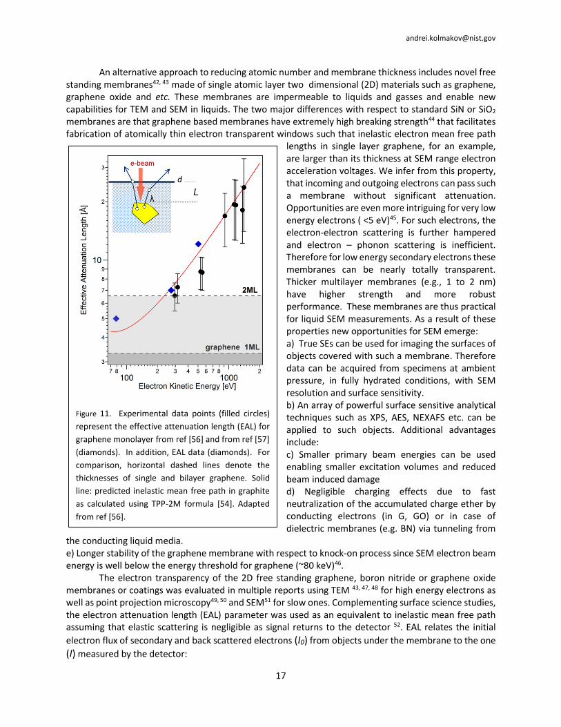
andreikolmakovnistgov
18
119868 1198680 = exp(minus(119871
120582119872+frasl
119889
120582119866)) (411)
here λG λM are EALs for graphene membrane and the media between the object and the membrane while d and L stand to thickness of corresponding layers as shown in the inset of Fig 11) This method is widely used to determine the thickness of overlayers for materials with known EALs53 Using this calculation EALs for graphene and graphene oxide were measured via collecting the substratersquos XPS54
55 AES56 and secondary electrons57 signals attenuated by the known amount of graphene or GO layers Fig 11 compiles some of this experimental data and compares them with theoretical predictions for carbon53 The reasonable agreement can be observed for the electrons acceleration voltages exceeding 70 eV EALs for energy ranges below this value have yet to be explored
442 Preparation of the graphene and graphene oxide membranes Graphene oxide (GO) was the first 2D material tested as an electron transparent window for SEM
E-cells54 58 The attractiveness of GO membranes stems from the well-developed high-yield GO production protocols of this material as discussed by Park and Rouff 59 and references therein Conveniently chemically exfoliated GO flakes have hydrophilic edges due to terminating COOH groups and hydrophobic basal plane due to the presence of domains of intact graphene Being amphiphilic GO flakes in water solutions segregate at air-water and water-solid interfaces to form membranes60 61 thus enabling Langmuir-Bludget or simple drop casting methods to be applied to fabricate suspended membrane When dried such membranes (often called GO-paper when thicker than few microns) have excellent 100 MPa 62 tensile strength that can be further enhanced by GO functionalization with divalent ions like Mg2+ and Ca2+63
Many different approaches to fabricate GO suspended membranes have been reported43 54 58 64 We have used diluted GO water or methanol solutions to cover micron wide orifices with a single flake of GO using LangmuirndashBlodgett deposition method54 This procedure can be repeated multiple times to fabricate multi-layer membranes Such membranes are molecular impermeable and mechanically sable under pressure differential if their diameter is below 3-5 microns Larger and therefore thicker membranes can be easily fabricated simply by drying of the GO solution over the small orifices58 Alternatively GO solution can be dried on the support which than can be suspended with a selective backside chemical or electrochemical etch58 64
As shown in recent reports64-66 GO membranes made of interlocked flakes have selective permeation properties that favor the capillary uptake and diffusion of water between stacked GO flakes GO permeation property results from GO flake separation distance d which is between 7Aring and 11 Aring depending on degree of GO reduction The flake separation distance is sufficient to accommodate one to two layers of water Interestingly such GO membranes are vacuum tight for many other gases and liquids such as atmospheric gases and alcohols64 This property makes GO excellent prospective material for selective filtering of media but a poor system for liquid water SEM experimental research To perform liquid SEM studies with GO membranes one can adopt several strategies (i) completely cover the orifice with an individual single layer or multilayer GO flake using the Lanmuir-Bludget approach (ii) adopt thicker GO membranes covering larger orifices that have less than one percolation channel inside the orifice The latter approach can be achieved by accounting for total length l and surface density s of the percolation
channels in GO membrane of thickness h scaling as 119897~ ℎ119871119889frasl and L-2 correspondingly where L is the average
size of the GO flake64 Thus the number N of the water conducting channels in an orifice of size D is
119873~(119863119871frasl )
2 Assuming the average size L of the GO flake in solution ~ 10 microns fabrication of GO water
impermeable multilayered electron transparent membranes can be done providing the size of the orifice D does not exceed L~10 microns58 Furthermore mildly annealed GO in the range between 120 and 150
andreikolmakovnistgov
19
degC eliminates the percolation water layers reducing d of the membrane without causing irreversible thermal reduction
Graphene on the other hand can be fabricated as a single layer carbon sheet and therefore is a nearly ideal material for e-cells since it is low atomic number has a small scattering cross section chemically inert ultrathin mechanically robust and lacks the aforementioned GO drawbacks The bulge and indentation tests demonstrated that suspended membranes are gas impermeable and yet have unprecedented robustness with stiffness in excess of 1 TPa67 what allows to sustain pressure differential of few Bars with diameters of the window below ca 5 microm
High quality large scale single and multi-layer graphene is routinely grown by CVD on Cu or Ni substrate and can be easily transferred to the substrate of interest by chemical etching of the substrate and via using PMMA film as sacrificial supporting layers Many other wet and dry transfer protocols were developed in recent years (see reviews 68 69 and references therein) As in the case of GO graphene membrane can be transferred on to the micron size apertures made by FiB micro pattering or laser drilling in the SiN SiO2 or metal supporting frame Graphene transfer processes involve removal of the interfacial liquid layer and residual contaminants from the graphene growth and release protocol This can be best done via slow annealing either in vacuum or under reducing (ArH2 mixture) ambient (see protocols in70) The annealing process also improves adhesion of Graphene to the substrate 443 Graphene and GO based E-cell design Two different graphene based closed cell designs have been tested as shown in Fig 12 The single use Si
based cell consisted of SiN primary membrane with FIB drilled micro-orifice LB covered with one or more graphene or GO layers The chip was filled with liquid sample and placed on a supporting Si plate (Fig 12a) Two part device are sealed with UV curable glueA silver paste patch is used to make a conductive ground for the device The principle design of the liquid cell with exchangeable graphene or GO windows is depicted in Fig 12 b The core of this E-
cell is a metal plate or SiNSi membrane with a laser or focused ion beam drilled hole for an aperture The standard PMMA based graphene transfer protocol was used to cover these 1-3 micron orifices Following deposition of graphene on the surface the system was annealed in air and PMMA was dissolved using warm acetone71 In the case of GO membranes the aforementioned Langmuir-Blodgett or drop casting protocols can be used to construct a membrane An exchangeable disk with a droplet of liquid sample is placed between two metal plates and vacuum sealed using pressure relief rubber membrane gasket The design of the cell allows isolation of a ca 20 μL sample and reduction of the pressure differential on to the graphene (GO) membrane when the liquid contains an excess of trapped gas and in vacuum
Figure 12 Principle design of closed graphenegraphene oxide E-cell a) single use cell b) refillable cell with exchangeable graphene (GO) membranes Adapted from refs [55] (a) and with permission from M Krueger et al ACS Nano 2011 5 10047-10054 Copyright (2011) American Chemical Society (b)
andreikolmakovnistgov
20
444 SEM imaging with GO and Graphene membranes The performance of the GO liquid cell filled with 50 nm Au colloid water solution can be evaluated
from the images in the Figure 13 a b Both images were obtained under the same SEM settings but using different detectors backscattered electrons detector (BSED Fig 13 panel (a)) and Everhart-Thornley detector (ETD Fig 13 panel (b)) which have larger and lower probing depth correspondingly Since ETD is sensitive to low energy secondary electrons greater detail of the membrane surface morphology (such as multiple GO wrinkles) can be seen The profile analysis of the gray scale values of the individual 50 nm Au
nanoparticles adhered to the back side of the ca 30 nm thick GO membrane (Figure 13 c) indicates that electron scattering in this low Z membrane does not deteriorate the resolution of the NP image significantly In addition to imaging EDX analysis can routinely be performed on a particles through the membrane as shown in the Fig 13 d
The examination of the gray scale variations taken with the ET detector as a function of the beam energy (not shown here) reveals the possibility for imaging high Z Au nanoparticles through the GO membrane using very low electron beam energies (starting from 1 keV) Since the thickness of the membrane (ca 30 nm) is an order of magnitude larger compared to inelastic mean free path for secondary electrons in GO54 detected electrons are backscattered and related secondary electrons of type S2 and S3 that compose SEM signal12
445 Radiation and
chemical stability of the graphene based membranes
Electron beam induced water radiolysis and radical generation is a significant effect in liquid electron microscopy and usually discussed in terms of impact on to the imaged objects Different from thick SiN membranes the direct defect formation or indirect beam induced chemical damage to thin 2D membranes are important issues in liquid SEM measurements since membrane damage limits the life time of the electron transparent windows of E-cells A selection of the available results are discussed below
The direct defect formation in the membranes can be due to electron induced atomic displacement (ldquoknock-onrdquo process) or as a result of relaxation of the electronic excitation inside the membrane The former mechanism has an energy threshold estimated to be 80 keV46 and is predicted to be inefficient at probe acceleration voltage energies used in SEM On the other hand the cross section for the inelastic electron excitation processes increases with lowered electron beam energies and is
Figure 13 a) SEM image of the Au NP solution through ca 40 nm thick GO membrane Image conditions beam energy 30 keV detector BSE tilt 39deg b) SEM taken under the same conditions but using Everhart-Thornley detector The scale bar corresponds to 5 microm c) Inset high resolution SEM image of two 50 nm Au nanoparticles immersed in water and adhered to the back side of the membrane Gray scale value line profile over the individual 50 nm Au nanoparticle d) EDX spectrum taken from Au NP aqueous solution through the GO membrane The red peaks correspond to Au lines and unmarked peaks originate from the surrounding stainless steel frame Adapted with permission from M Krueger et al ACS Nano 2011 5 10047-10054 Copyright (2011) American Chemical Society
andreikolmakovnistgov
21
significant at low keV acceleration voltages This damage mechanism can result in chemical bonds breakage and local heating The thermal conductivity of the graphene at room temperature is high (ca 5000 WmmiddotK)72 and no noticeable damage due to electron beam heating effect is expected This damage mechanism is even less probable when gaseous or liquid media is in contact with 2D membrane
For practical SEM imaging through 2D membranes it is important to know these threshold doses of noticeable electron induced defect formation and to minimize all aforementioned effects via reducing the electron beam exposure Beam exposure effects is difficult to define as there is significant variation in published experimental data experimental conditions and often dose measurements are not recorded in SEM experiments This issue is further complicated by a variety of energy dissipation mechanisms during e-beam irradiation of hydrated samples GO membranes were found to be prone for photo-thermal reduction with a flash light 73 74 and laser light illumination A characteristic threshold was measured to be ca 102 mJ cm2 for a micron thick GO membrane73 corresponding to an electron beam dose of ca 1 enm2 for 10 keV electrons assuming full absorption of probe beam energy by the film Alternative results indicate that GO films did not suffer reduction from a 20 keV electron probe beam until reaching doses as high as 103 enm2
75 Data is also available for electron beam induced damage of graphene layers from SEM
imaging and electron beam lithography It has been observed for graphene field effect transistors (GFETs) that the appearance and growth of the disorder D peak in Raman spectrum of the supported graphene as well as concomitant increase of its resistivity (mobility drop) occur after irradiation with doses as low as 20 enm2 76 Bi-layer graphene was found to be significantly more stable to radiation damage Similar measurements on the suspended graphene FET demonstrated considerably smaller change of the electronic properties upon even larger (102 enm2) irradiation doses while the growth of the DG Raman peaks ratio remained nearly the same as in the case of supported graphene77 The latter observation implies that the observed changes in Raman signatures or electron mobility can be due to beam induced modification (eg local charging) of the supporting substrate or electron beam induced carbonization of the graphene layer 78 but not due to massive defect formation in the graphene itself
The presence of the dense gaseous or liquid media in contact with graphene (or GO) can catalyze the formation of new or develop pre-existing defects indirectly via generation of ionic or radical species that attack 2D membrane chemically As it has been shown recently in STM studies of water exposed to graphene this is particularly relevant to linear defects and grain boundaries in this material79 Another example is reduction of the GO by electron beam generation of plasmas produced in inert (Ar) reducing gases (CH4) or their mixtures80 Similar processes occur in water during beam induced water radiolysis which has been extensively studied (eg ref 81 and references therein) Chemically reactive products such as molecular hydrogen (H2) hydrogen peroxide (H2O2) and hydroxyl radicals (OH) produced in water by radiolysis can accumulate 81 and reduce or oxidize the 2D membrane weakening or dissociating C-C bonds at defects sites In addition under prolonged exposure volatile products of radiolysis can eventually segregate as a separate phase forming microbubble under 2D membrane potentially leading to a pressure buildup inside the E-cell and capillary induced collapse of the membrane We estimated that 20 keV electron beam irradiation of liquid water under the graphene membrane leads to bubble formation following accumulation of critical dose of ~104 enm2 55 82 SEM operation below bubble forming dose levels enables good image acquisition conditions as data maybe be acquired at dose levels of (~102 enm2) from illumination areas ca ~102 microm2 This problem can be further reduced in fluidic cells where replenishable solution is used thus enabling removal of radiolysis byproduct from the probe beam scan area
Outlook Nanoscale imaging in liquids and at solid- gas -liquid interfaces enables research in the fields of materials science biomedical forensics chemistry and environmental research We expect membrane based liquid scanning electron microscopy be a growing field of research in years to come Based on the current trends
andreikolmakovnistgov
22
one can envision three different lines of near future activities and developments of this microscopy modality
1 Theory modelling and fundamental research on chemistry and physical aspects of the electron beam interaction with liquid matter and immersed objects This research includes the understanding of beam induced local chemistry in liquids and dense gases spatial and temporal distributions of reactive species and their possible influence on the immersed objects The probing of the different systems such as operational electrochemical and fuel cells as well as living biological objects will continue along with the efforts to minimize beam induced artifacts via improving the sensitivity of the detectors and implementation of modern image processing and data mining algorithms There is also clear trend to combine different imaging modalities
2 Liquid cells designs The electron transparent windows with the thickness of 20-50 nm based on modern SiN SiO2 or SiC microfabrication processes will be a dominating technological platform for near future liquid SEM The variety of experimental tasks and objects makes it almost impossible to create a universal liquid SEM cell therefore similar to modern liquid TEM trends some degree of specialization in the cell will take place For example fabrication of SiN electron transparent windows dedicated to electrochemical variable temperature studies in situ
micromanipulation and electrical measurements can be envisioned The overall design of the future liquid cells will be single use monolithic chip with so-called on board fluidics where the source liquids and electrophoretic electroosmotic or micromechanical pumps are integral parts of the lab-on-chip liquid SEM technology 3 Membranes development Novel 2D materials with ultimately high electron transparency and mechanical strength will remain the object of active research and technical developments The driving force behind this line of the research is the unique capability to use powerful surface characterization techniques for liquid interfaces such as XPS55 The combination of the requirement to have large FOV with micron size graphene covered orifices will result in implementation of a new environmental cell platform where the membrane is composed of multiple orifices One of the possible designs of
the graphene based liquid cell is proposed in the Fig 14 The core of the cell is multichannel or microporous matrix which contains high density isolated or interconnected microfluidic channels The channels have openings which are covered with graphene membrane Such a cell can be equipped with heaters and electrodes as well channels can be impregnated with different liquids (A-D Figure 14) Such a design is favorable for the combinatorial SEM studies with correlative electron (eg XPS AES) or optical (cathodoluminescence (CL) IR Vis) spectroscopies Disclaimer Certain commercial equipment instruments or materials are identified in this paper in order to demonstrate the experimental procedures and capabilities adequately Such identification is not intended to imply recommendation or endorsement by the National Institute of Standards and Technology nor is it intended to imply that the materials or equipment identified are necessarily the best available for the purpose
Figure 14 Prospective design of the microchannel sample
platform for liquid SEM through the array of the graphene
covered micro-orifices Adapted from ref[55]
andreikolmakovnistgov
23
Disclaimer Official contribution of the National Institute of Standards and Technology not subject to copyright in the United States Acknowledgements AK thanks his SIUC students Shannon Berg Mark Krueger Joshua Cothren Joshua Stoll and Alexander Yulaev whose work became the base of this chapter The technical discussions with Christopher Brown Alex Liddle Dr Renu Sharma and Nikolai Zhitentev (all at NIST) are greatly appreciated References 1 G D Danilatos Inst Phys Conf Ser 1990 455-458 2 G D Dantilatos US Patent 4596928 1986 3 A Bogner G Thollet D Basset P-H Jouneau and C Gauthier Ultramicroscopy 2005 104 290-
301 4 I Abrams and J McBain Journal of Applied Physics 1944 15 607-609 5 S Thiberge O Zik and E Moses Review of Scientific Instruments 2004 75 2280-2289 6 M Suga H Nishiyama Y Konyuba S Iwamatsu Y Watanabe C Yoshiura T Ueda and C Sato
Ultramicroscopy 2011 111 1650-1658 7 N Vidavsky S Addadi J Mahamid E Shimoni D Ben-Ezra M Shpigel S Weiner and L Addadi
Proceedings of the National Academy of Sciences 2014 111 39-44 8 Y Ominami S Kawanishi T Ushiki and S Ito Microscopy 2014 dfu107 9 E Jensen A Burrows and K Moslashlhave Microscopy and Microanalysis 2014 20 445-451 10 H Demers N Poirier‐Demers A R Couture D Joly M Guilmain N de Jonge and D Drouin
Scanning 2011 33 135-146 11 K Kanaya and S Okayama Journal of Physics D Applied Physics 1972 5 43 12 J Goldstein D Newbury D Joy C Lyman P Echlin E Lifshin L Sawyer and J Michael 2003 13 R Egerton P Li and M Malac Micron 2004 35 399-409 14 D A Fischer D H Alsem B Simon T Prozorov and N Salmon Microscopy and Microanalysis
2013 19 476-477 15 V Behar O Gileadi Y Karni Y Kliger A Nechushtan D Sprinzak and O Zik US patent 7230242
B2 2007 16 S Thiberge A Nechushtan D Sprinzak O Gileadi V Behar O Zik Y Chowers S Michaeli J
Schlessinger and E Moses Proceedings of the National Academy of Sciences of the United States of America 2004 101 3346-3351
17 G Venkiteela and Z H Sun Cement amp Concrete Composites 2010 32 211-218 18 K Tiede S P Tear H David and A B A Boxall Water Research 2009 43 3335-3343 19 B G Mathapa and V N Paunov Physical Chemistry Chemical Physics 2013 15 17903-17914 20 C Lorenz K Tiede S Tear A Boxall N von Goetz and K Hungerbuhler International Journal of
Occupational and Environmental Health 2010 16 406-428 21 D C Joy and C S Joy Journal of Microscopy-Oxford 2006 221 84-88 22 A K F Dyab and V N Paunov Soft Matter 2010 6 2613-2615 23 O Cohen R Beery S Levit J Ilany I Schwartz M Shabtai D Anaby D Cohen R Alfici A
Czerniak and A Karasik Thyroid 2006 16 997-1001 24 N Kolmakova and A Kolmakov The Journal of Physical Chemistry C 2010 114 17233-17237 25 C Wei W Y Lin Z Zainal N E Williams K Zhu A P Kruzic R L Smith and K Rajeshwar
Environmental science amp technology 1994 28 934-938 26 J L Giocondi and G S Rohrer Topics in catalysis 2008 49 18-23
andreikolmakovnistgov
24
27 J M Herrmann Catalysis Today 1999 53 115-129 28 J Geisler-Lee Q Wang Y Yao W Zhang M Geisler K Li Y Huang Y Chen A Kolmakov and X
Ma Nanotoxicology 2012 7 323-337 29 N M Schneider M M Norton B J Mendel J M Grogan F M Ross and H H Bau The Journal
of Physical Chemistry C 2014 118 22373-22382 30 E U Donev and J T Hastings Nano letters 2009 9 2715-2718 31 A Al-Asadi J Zhang J Li R A Potyrailo and A Kolmakov arXiv preprint arXiv150100762
2015 32 C Monat P Domachuk and B Eggleton Nature photonics 2007 1 106-114 33 D Erickson D Sinton and D Psaltis Nature Photonics 2011 5 583-590 34 R A Potyrailo H Ghiradella A Vertiatchikh K Dovidenko J R Cournoyer and E Olson Nature
Photonics 2007 1 123-128 35 R A Potyrailo T A Starkey P Vukusic H Ghiradella M Vasudev T Bunning R R Naik Z
Tang M Larsen and T Deng Proceedings of the National Academy of Sciences 2013 110 15567-15572
36 R R Unocic X-G Sun R L Sacci L A Adamczyk D H Alsem S Dai N J Dudney and K L More Microscopy and Microanalysis 2014 20 1029-1037
37 K Klein I Anderson and N De Jonge Journal of microscopy 2011 242 117-123 38 K Moslashlhave C Kallesoslashe C Wen F Ross T Booth T Kjoslashller Nellemann E Jensen C Elkjaeligr J
Rasmussen and P Jensen Microscopy and Microanalysis 2010 16 322-323 39 J E Cothren Thesis Master of Science Southern Illinois University Carbondale 2011 40 Y Liu Master of Science Southern Illinois University at Carbondale 2013 41 S Ueda Y Kobayashi S Koizumi and Y Tsutsumi Microscopy 2014 dfu100 42 J C Meyer A K Geim M Katsnelson K Novoselov T Booth and S Roth Nature 2007 446
60-63 43 N R Wilson P A Pandey R Beanland R J Young I A Kinloch L Gong Z Liu K Suenaga J P
Rourke and S J York ACS nano 2009 3 2547-2556 44 C Lee X Wei J W Kysar and J Hone science 2008 321 385-388 45 I Muumlllerovaacute M Hovorka and L Frank Ultramicroscopy 2012 119 78-81 46 J C Meyer F Eder S Kurasch V Skakalova J Kotakoski H J Park S Roth A Chuvilin S
Eyhusen and G Benner Physical review letters 2012 108 196102 47 J C Meyer C O Girit M Crommie and A Zettl Nature 2008 454 319-322 48 R S Pantelic J C Meyer U Kaiser and H Stahlberg Solid State Communications 2012 152
1375-1382 49 J Mutus L Livadaru J Robinson R Urban M Salomons M Cloutier and R Wolkow New
Journal of Physics 2011 13 063011 50 J-N Longchamp C Escher T Latychevskaia and H-W Fink Ultramicroscopy 2014 51 L Frank E Mikmekovaacute I Muumlllerovaacute and M Lejeune Applied Physics Letters 2015 106 013117 52 A Jablonski and C Powell Journal of Vacuum Science amp Technology A Vacuum Surfaces and
Films 2009 27 253-261 53 S Tanuma C Powell and D Penn Surface and Interface Analysis 2011 43 689-713 54 A Kolmakov D A Dikin L J Cote J X Huang M K Abyaneh M Amati L Gregoratti S
Gunther and M Kiskinova Nature Nanotechnology 2011 6 651-657 55 J Kraus R Reichelt S Guenther L Gregoratti M Amati M Kiskinova A Yulaev I Vlassiokiv
and A Kolmakov Nanoscale 2014 56 M Xu D Fujita J Gao and N Hanagata Acs Nano 2010 4 2937-2945 57 V Kochat A N Pal E Sneha A Sampathkumar A Gairola S Shivashankar S Raghavan and A
Ghosh Journal of Applied Physics 2011 110 014315
andreikolmakovnistgov
25
58 M Krueger S Berg D Stone E Strelcov D A Dikin J Kim L J Cote J X Huang and A Kolmakov Acs Nano 2011 5 10047-10054
59 S Park and R S Ruoff Nature nanotechnology 2009 4 217-224 60 D Li M B Muumlller S Gilje R B Kaner and G G Wallace Nature nanotechnology 2008 3 101-
105 61 L J Cote J Kim V C Tung J Luo F Kim and J Huang Pure and Applied Chemistry 2010 83
95-110 62 D A Dikin S Stankovich E J Zimney R D Piner G H Dommett G Evmenenko S T Nguyen
and R S Ruoff Nature 2007 448 457-460 63 S Park K-S Lee G Bozoklu W Cai S T Nguyen and R S Ruoff ACS nano 2008 2 572-578 64 R Nair H Wu P Jayaram I Grigorieva and A Geim Science 2012 335 442-444 65 H W Kim H W Yoon S-M Yoon B M Yoo B K Ahn Y H Cho H J Shin H Yang U Paik and
S Kwon Science 2013 342 91-95 66 R Joshi P Carbone F Wang V Kravets Y Su I Grigorieva H Wu A Geim and R Nair Science
2014 343 752-754 67 J S Bunch S S Verbridge J S Alden A M van der Zande J M Parpia H G Craighead and P
L McEuen Nano letters 2008 8 2458-2462 68 J Kang D Shin S Bae and B H Hong Nanoscale 2012 4 5527-5537 69 F Bonaccorso A Lombardo T Hasan Z Sun L Colombo and A C Ferrari Materials Today
2012 15 564-589 70 Y-C Lin C-C Lu C-H Yeh C Jin K Suenaga and P-W Chiu Nano letters 2011 12 414-419 71 J W Suk A Kitt C W Magnuson Y Hao S Ahmed J An A K Swan B B Goldberg and R S
Ruoff ACS nano 2011 5 6916-6924 72 A A Balandin S Ghosh W Bao I Calizo D Teweldebrhan F Miao and C N Lau Nano letters
2008 8 902-907 73 L J Cote R Cruz-Silva and J Huang Journal of the American Chemical Society 2009 131
11027-11032 74 S Gilje S Dubin A Badakhshan J Farrar S Danczyk and R B Kaner Advanced Materials 2010
22 419-423 75 P Kumar K Subrahmanyam and C Rao Materials Express 2011 1 252-256 76 G Liu D Teweldebrhan and A A Balandin Nanotechnology IEEE Transactions on 2011 10
865-870 77 I Childres L A Jauregui M Foxe J Tian R Jalilian I Jovanovic and Y P Chen Applied Physics
Letters 2010 97 173109 78 L Tao C Qiu F Yu H Yang M Chen G Wang and L Sun The Journal of Physical Chemistry C
2013 117 10079-10085 79 X Feng S Maier and M Salmeron Journal of the American Chemical Society 2012 134 5662-
5668 80 M Baraket S Walton Z Wei E Lock J Robinson and P Sheehan Carbon 2010 48 3382-3390 81 C Royall B Thiel and A Donald Journal of Microscopy 2001 204 185-195 82 J D Stoll and A Kolmakov Nanotechnology 2012 23
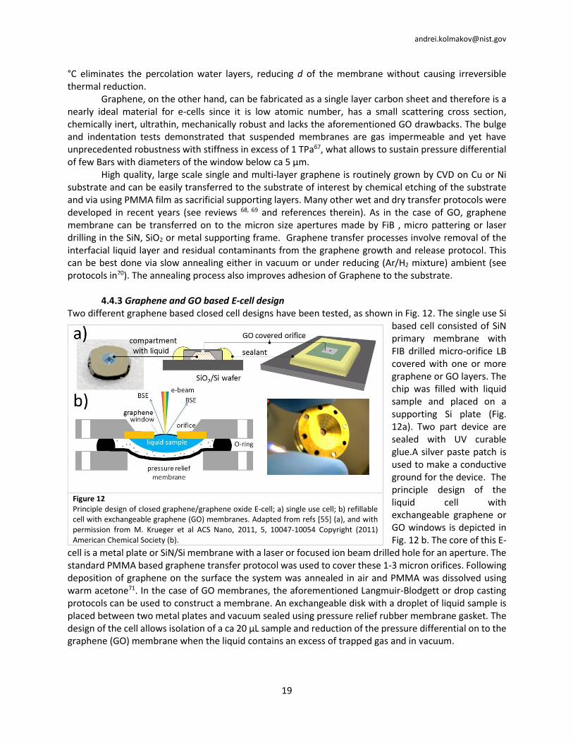
andreikolmakovnistgov
19
degC eliminates the percolation water layers reducing d of the membrane without causing irreversible thermal reduction
Graphene on the other hand can be fabricated as a single layer carbon sheet and therefore is a nearly ideal material for e-cells since it is low atomic number has a small scattering cross section chemically inert ultrathin mechanically robust and lacks the aforementioned GO drawbacks The bulge and indentation tests demonstrated that suspended membranes are gas impermeable and yet have unprecedented robustness with stiffness in excess of 1 TPa67 what allows to sustain pressure differential of few Bars with diameters of the window below ca 5 microm
High quality large scale single and multi-layer graphene is routinely grown by CVD on Cu or Ni substrate and can be easily transferred to the substrate of interest by chemical etching of the substrate and via using PMMA film as sacrificial supporting layers Many other wet and dry transfer protocols were developed in recent years (see reviews 68 69 and references therein) As in the case of GO graphene membrane can be transferred on to the micron size apertures made by FiB micro pattering or laser drilling in the SiN SiO2 or metal supporting frame Graphene transfer processes involve removal of the interfacial liquid layer and residual contaminants from the graphene growth and release protocol This can be best done via slow annealing either in vacuum or under reducing (ArH2 mixture) ambient (see protocols in70) The annealing process also improves adhesion of Graphene to the substrate 443 Graphene and GO based E-cell design Two different graphene based closed cell designs have been tested as shown in Fig 12 The single use Si
based cell consisted of SiN primary membrane with FIB drilled micro-orifice LB covered with one or more graphene or GO layers The chip was filled with liquid sample and placed on a supporting Si plate (Fig 12a) Two part device are sealed with UV curable glueA silver paste patch is used to make a conductive ground for the device The principle design of the liquid cell with exchangeable graphene or GO windows is depicted in Fig 12 b The core of this E-
cell is a metal plate or SiNSi membrane with a laser or focused ion beam drilled hole for an aperture The standard PMMA based graphene transfer protocol was used to cover these 1-3 micron orifices Following deposition of graphene on the surface the system was annealed in air and PMMA was dissolved using warm acetone71 In the case of GO membranes the aforementioned Langmuir-Blodgett or drop casting protocols can be used to construct a membrane An exchangeable disk with a droplet of liquid sample is placed between two metal plates and vacuum sealed using pressure relief rubber membrane gasket The design of the cell allows isolation of a ca 20 μL sample and reduction of the pressure differential on to the graphene (GO) membrane when the liquid contains an excess of trapped gas and in vacuum
Figure 12 Principle design of closed graphenegraphene oxide E-cell a) single use cell b) refillable cell with exchangeable graphene (GO) membranes Adapted from refs [55] (a) and with permission from M Krueger et al ACS Nano 2011 5 10047-10054 Copyright (2011) American Chemical Society (b)
andreikolmakovnistgov
20
444 SEM imaging with GO and Graphene membranes The performance of the GO liquid cell filled with 50 nm Au colloid water solution can be evaluated
from the images in the Figure 13 a b Both images were obtained under the same SEM settings but using different detectors backscattered electrons detector (BSED Fig 13 panel (a)) and Everhart-Thornley detector (ETD Fig 13 panel (b)) which have larger and lower probing depth correspondingly Since ETD is sensitive to low energy secondary electrons greater detail of the membrane surface morphology (such as multiple GO wrinkles) can be seen The profile analysis of the gray scale values of the individual 50 nm Au
nanoparticles adhered to the back side of the ca 30 nm thick GO membrane (Figure 13 c) indicates that electron scattering in this low Z membrane does not deteriorate the resolution of the NP image significantly In addition to imaging EDX analysis can routinely be performed on a particles through the membrane as shown in the Fig 13 d
The examination of the gray scale variations taken with the ET detector as a function of the beam energy (not shown here) reveals the possibility for imaging high Z Au nanoparticles through the GO membrane using very low electron beam energies (starting from 1 keV) Since the thickness of the membrane (ca 30 nm) is an order of magnitude larger compared to inelastic mean free path for secondary electrons in GO54 detected electrons are backscattered and related secondary electrons of type S2 and S3 that compose SEM signal12
445 Radiation and
chemical stability of the graphene based membranes
Electron beam induced water radiolysis and radical generation is a significant effect in liquid electron microscopy and usually discussed in terms of impact on to the imaged objects Different from thick SiN membranes the direct defect formation or indirect beam induced chemical damage to thin 2D membranes are important issues in liquid SEM measurements since membrane damage limits the life time of the electron transparent windows of E-cells A selection of the available results are discussed below
The direct defect formation in the membranes can be due to electron induced atomic displacement (ldquoknock-onrdquo process) or as a result of relaxation of the electronic excitation inside the membrane The former mechanism has an energy threshold estimated to be 80 keV46 and is predicted to be inefficient at probe acceleration voltage energies used in SEM On the other hand the cross section for the inelastic electron excitation processes increases with lowered electron beam energies and is
Figure 13 a) SEM image of the Au NP solution through ca 40 nm thick GO membrane Image conditions beam energy 30 keV detector BSE tilt 39deg b) SEM taken under the same conditions but using Everhart-Thornley detector The scale bar corresponds to 5 microm c) Inset high resolution SEM image of two 50 nm Au nanoparticles immersed in water and adhered to the back side of the membrane Gray scale value line profile over the individual 50 nm Au nanoparticle d) EDX spectrum taken from Au NP aqueous solution through the GO membrane The red peaks correspond to Au lines and unmarked peaks originate from the surrounding stainless steel frame Adapted with permission from M Krueger et al ACS Nano 2011 5 10047-10054 Copyright (2011) American Chemical Society
andreikolmakovnistgov
21
significant at low keV acceleration voltages This damage mechanism can result in chemical bonds breakage and local heating The thermal conductivity of the graphene at room temperature is high (ca 5000 WmmiddotK)72 and no noticeable damage due to electron beam heating effect is expected This damage mechanism is even less probable when gaseous or liquid media is in contact with 2D membrane
For practical SEM imaging through 2D membranes it is important to know these threshold doses of noticeable electron induced defect formation and to minimize all aforementioned effects via reducing the electron beam exposure Beam exposure effects is difficult to define as there is significant variation in published experimental data experimental conditions and often dose measurements are not recorded in SEM experiments This issue is further complicated by a variety of energy dissipation mechanisms during e-beam irradiation of hydrated samples GO membranes were found to be prone for photo-thermal reduction with a flash light 73 74 and laser light illumination A characteristic threshold was measured to be ca 102 mJ cm2 for a micron thick GO membrane73 corresponding to an electron beam dose of ca 1 enm2 for 10 keV electrons assuming full absorption of probe beam energy by the film Alternative results indicate that GO films did not suffer reduction from a 20 keV electron probe beam until reaching doses as high as 103 enm2
75 Data is also available for electron beam induced damage of graphene layers from SEM
imaging and electron beam lithography It has been observed for graphene field effect transistors (GFETs) that the appearance and growth of the disorder D peak in Raman spectrum of the supported graphene as well as concomitant increase of its resistivity (mobility drop) occur after irradiation with doses as low as 20 enm2 76 Bi-layer graphene was found to be significantly more stable to radiation damage Similar measurements on the suspended graphene FET demonstrated considerably smaller change of the electronic properties upon even larger (102 enm2) irradiation doses while the growth of the DG Raman peaks ratio remained nearly the same as in the case of supported graphene77 The latter observation implies that the observed changes in Raman signatures or electron mobility can be due to beam induced modification (eg local charging) of the supporting substrate or electron beam induced carbonization of the graphene layer 78 but not due to massive defect formation in the graphene itself
The presence of the dense gaseous or liquid media in contact with graphene (or GO) can catalyze the formation of new or develop pre-existing defects indirectly via generation of ionic or radical species that attack 2D membrane chemically As it has been shown recently in STM studies of water exposed to graphene this is particularly relevant to linear defects and grain boundaries in this material79 Another example is reduction of the GO by electron beam generation of plasmas produced in inert (Ar) reducing gases (CH4) or their mixtures80 Similar processes occur in water during beam induced water radiolysis which has been extensively studied (eg ref 81 and references therein) Chemically reactive products such as molecular hydrogen (H2) hydrogen peroxide (H2O2) and hydroxyl radicals (OH) produced in water by radiolysis can accumulate 81 and reduce or oxidize the 2D membrane weakening or dissociating C-C bonds at defects sites In addition under prolonged exposure volatile products of radiolysis can eventually segregate as a separate phase forming microbubble under 2D membrane potentially leading to a pressure buildup inside the E-cell and capillary induced collapse of the membrane We estimated that 20 keV electron beam irradiation of liquid water under the graphene membrane leads to bubble formation following accumulation of critical dose of ~104 enm2 55 82 SEM operation below bubble forming dose levels enables good image acquisition conditions as data maybe be acquired at dose levels of (~102 enm2) from illumination areas ca ~102 microm2 This problem can be further reduced in fluidic cells where replenishable solution is used thus enabling removal of radiolysis byproduct from the probe beam scan area
Outlook Nanoscale imaging in liquids and at solid- gas -liquid interfaces enables research in the fields of materials science biomedical forensics chemistry and environmental research We expect membrane based liquid scanning electron microscopy be a growing field of research in years to come Based on the current trends
andreikolmakovnistgov
22
one can envision three different lines of near future activities and developments of this microscopy modality
1 Theory modelling and fundamental research on chemistry and physical aspects of the electron beam interaction with liquid matter and immersed objects This research includes the understanding of beam induced local chemistry in liquids and dense gases spatial and temporal distributions of reactive species and their possible influence on the immersed objects The probing of the different systems such as operational electrochemical and fuel cells as well as living biological objects will continue along with the efforts to minimize beam induced artifacts via improving the sensitivity of the detectors and implementation of modern image processing and data mining algorithms There is also clear trend to combine different imaging modalities
2 Liquid cells designs The electron transparent windows with the thickness of 20-50 nm based on modern SiN SiO2 or SiC microfabrication processes will be a dominating technological platform for near future liquid SEM The variety of experimental tasks and objects makes it almost impossible to create a universal liquid SEM cell therefore similar to modern liquid TEM trends some degree of specialization in the cell will take place For example fabrication of SiN electron transparent windows dedicated to electrochemical variable temperature studies in situ
micromanipulation and electrical measurements can be envisioned The overall design of the future liquid cells will be single use monolithic chip with so-called on board fluidics where the source liquids and electrophoretic electroosmotic or micromechanical pumps are integral parts of the lab-on-chip liquid SEM technology 3 Membranes development Novel 2D materials with ultimately high electron transparency and mechanical strength will remain the object of active research and technical developments The driving force behind this line of the research is the unique capability to use powerful surface characterization techniques for liquid interfaces such as XPS55 The combination of the requirement to have large FOV with micron size graphene covered orifices will result in implementation of a new environmental cell platform where the membrane is composed of multiple orifices One of the possible designs of
the graphene based liquid cell is proposed in the Fig 14 The core of the cell is multichannel or microporous matrix which contains high density isolated or interconnected microfluidic channels The channels have openings which are covered with graphene membrane Such a cell can be equipped with heaters and electrodes as well channels can be impregnated with different liquids (A-D Figure 14) Such a design is favorable for the combinatorial SEM studies with correlative electron (eg XPS AES) or optical (cathodoluminescence (CL) IR Vis) spectroscopies Disclaimer Certain commercial equipment instruments or materials are identified in this paper in order to demonstrate the experimental procedures and capabilities adequately Such identification is not intended to imply recommendation or endorsement by the National Institute of Standards and Technology nor is it intended to imply that the materials or equipment identified are necessarily the best available for the purpose
Figure 14 Prospective design of the microchannel sample
platform for liquid SEM through the array of the graphene
covered micro-orifices Adapted from ref[55]
andreikolmakovnistgov
23
Disclaimer Official contribution of the National Institute of Standards and Technology not subject to copyright in the United States Acknowledgements AK thanks his SIUC students Shannon Berg Mark Krueger Joshua Cothren Joshua Stoll and Alexander Yulaev whose work became the base of this chapter The technical discussions with Christopher Brown Alex Liddle Dr Renu Sharma and Nikolai Zhitentev (all at NIST) are greatly appreciated References 1 G D Danilatos Inst Phys Conf Ser 1990 455-458 2 G D Dantilatos US Patent 4596928 1986 3 A Bogner G Thollet D Basset P-H Jouneau and C Gauthier Ultramicroscopy 2005 104 290-
301 4 I Abrams and J McBain Journal of Applied Physics 1944 15 607-609 5 S Thiberge O Zik and E Moses Review of Scientific Instruments 2004 75 2280-2289 6 M Suga H Nishiyama Y Konyuba S Iwamatsu Y Watanabe C Yoshiura T Ueda and C Sato
Ultramicroscopy 2011 111 1650-1658 7 N Vidavsky S Addadi J Mahamid E Shimoni D Ben-Ezra M Shpigel S Weiner and L Addadi
Proceedings of the National Academy of Sciences 2014 111 39-44 8 Y Ominami S Kawanishi T Ushiki and S Ito Microscopy 2014 dfu107 9 E Jensen A Burrows and K Moslashlhave Microscopy and Microanalysis 2014 20 445-451 10 H Demers N Poirier‐Demers A R Couture D Joly M Guilmain N de Jonge and D Drouin
Scanning 2011 33 135-146 11 K Kanaya and S Okayama Journal of Physics D Applied Physics 1972 5 43 12 J Goldstein D Newbury D Joy C Lyman P Echlin E Lifshin L Sawyer and J Michael 2003 13 R Egerton P Li and M Malac Micron 2004 35 399-409 14 D A Fischer D H Alsem B Simon T Prozorov and N Salmon Microscopy and Microanalysis
2013 19 476-477 15 V Behar O Gileadi Y Karni Y Kliger A Nechushtan D Sprinzak and O Zik US patent 7230242
B2 2007 16 S Thiberge A Nechushtan D Sprinzak O Gileadi V Behar O Zik Y Chowers S Michaeli J
Schlessinger and E Moses Proceedings of the National Academy of Sciences of the United States of America 2004 101 3346-3351
17 G Venkiteela and Z H Sun Cement amp Concrete Composites 2010 32 211-218 18 K Tiede S P Tear H David and A B A Boxall Water Research 2009 43 3335-3343 19 B G Mathapa and V N Paunov Physical Chemistry Chemical Physics 2013 15 17903-17914 20 C Lorenz K Tiede S Tear A Boxall N von Goetz and K Hungerbuhler International Journal of
Occupational and Environmental Health 2010 16 406-428 21 D C Joy and C S Joy Journal of Microscopy-Oxford 2006 221 84-88 22 A K F Dyab and V N Paunov Soft Matter 2010 6 2613-2615 23 O Cohen R Beery S Levit J Ilany I Schwartz M Shabtai D Anaby D Cohen R Alfici A
Czerniak and A Karasik Thyroid 2006 16 997-1001 24 N Kolmakova and A Kolmakov The Journal of Physical Chemistry C 2010 114 17233-17237 25 C Wei W Y Lin Z Zainal N E Williams K Zhu A P Kruzic R L Smith and K Rajeshwar
Environmental science amp technology 1994 28 934-938 26 J L Giocondi and G S Rohrer Topics in catalysis 2008 49 18-23
andreikolmakovnistgov
24
27 J M Herrmann Catalysis Today 1999 53 115-129 28 J Geisler-Lee Q Wang Y Yao W Zhang M Geisler K Li Y Huang Y Chen A Kolmakov and X
Ma Nanotoxicology 2012 7 323-337 29 N M Schneider M M Norton B J Mendel J M Grogan F M Ross and H H Bau The Journal
of Physical Chemistry C 2014 118 22373-22382 30 E U Donev and J T Hastings Nano letters 2009 9 2715-2718 31 A Al-Asadi J Zhang J Li R A Potyrailo and A Kolmakov arXiv preprint arXiv150100762
2015 32 C Monat P Domachuk and B Eggleton Nature photonics 2007 1 106-114 33 D Erickson D Sinton and D Psaltis Nature Photonics 2011 5 583-590 34 R A Potyrailo H Ghiradella A Vertiatchikh K Dovidenko J R Cournoyer and E Olson Nature
Photonics 2007 1 123-128 35 R A Potyrailo T A Starkey P Vukusic H Ghiradella M Vasudev T Bunning R R Naik Z
Tang M Larsen and T Deng Proceedings of the National Academy of Sciences 2013 110 15567-15572
36 R R Unocic X-G Sun R L Sacci L A Adamczyk D H Alsem S Dai N J Dudney and K L More Microscopy and Microanalysis 2014 20 1029-1037
37 K Klein I Anderson and N De Jonge Journal of microscopy 2011 242 117-123 38 K Moslashlhave C Kallesoslashe C Wen F Ross T Booth T Kjoslashller Nellemann E Jensen C Elkjaeligr J
Rasmussen and P Jensen Microscopy and Microanalysis 2010 16 322-323 39 J E Cothren Thesis Master of Science Southern Illinois University Carbondale 2011 40 Y Liu Master of Science Southern Illinois University at Carbondale 2013 41 S Ueda Y Kobayashi S Koizumi and Y Tsutsumi Microscopy 2014 dfu100 42 J C Meyer A K Geim M Katsnelson K Novoselov T Booth and S Roth Nature 2007 446
60-63 43 N R Wilson P A Pandey R Beanland R J Young I A Kinloch L Gong Z Liu K Suenaga J P
Rourke and S J York ACS nano 2009 3 2547-2556 44 C Lee X Wei J W Kysar and J Hone science 2008 321 385-388 45 I Muumlllerovaacute M Hovorka and L Frank Ultramicroscopy 2012 119 78-81 46 J C Meyer F Eder S Kurasch V Skakalova J Kotakoski H J Park S Roth A Chuvilin S
Eyhusen and G Benner Physical review letters 2012 108 196102 47 J C Meyer C O Girit M Crommie and A Zettl Nature 2008 454 319-322 48 R S Pantelic J C Meyer U Kaiser and H Stahlberg Solid State Communications 2012 152
1375-1382 49 J Mutus L Livadaru J Robinson R Urban M Salomons M Cloutier and R Wolkow New
Journal of Physics 2011 13 063011 50 J-N Longchamp C Escher T Latychevskaia and H-W Fink Ultramicroscopy 2014 51 L Frank E Mikmekovaacute I Muumlllerovaacute and M Lejeune Applied Physics Letters 2015 106 013117 52 A Jablonski and C Powell Journal of Vacuum Science amp Technology A Vacuum Surfaces and
Films 2009 27 253-261 53 S Tanuma C Powell and D Penn Surface and Interface Analysis 2011 43 689-713 54 A Kolmakov D A Dikin L J Cote J X Huang M K Abyaneh M Amati L Gregoratti S
Gunther and M Kiskinova Nature Nanotechnology 2011 6 651-657 55 J Kraus R Reichelt S Guenther L Gregoratti M Amati M Kiskinova A Yulaev I Vlassiokiv
and A Kolmakov Nanoscale 2014 56 M Xu D Fujita J Gao and N Hanagata Acs Nano 2010 4 2937-2945 57 V Kochat A N Pal E Sneha A Sampathkumar A Gairola S Shivashankar S Raghavan and A
Ghosh Journal of Applied Physics 2011 110 014315
andreikolmakovnistgov
25
58 M Krueger S Berg D Stone E Strelcov D A Dikin J Kim L J Cote J X Huang and A Kolmakov Acs Nano 2011 5 10047-10054
59 S Park and R S Ruoff Nature nanotechnology 2009 4 217-224 60 D Li M B Muumlller S Gilje R B Kaner and G G Wallace Nature nanotechnology 2008 3 101-
105 61 L J Cote J Kim V C Tung J Luo F Kim and J Huang Pure and Applied Chemistry 2010 83
95-110 62 D A Dikin S Stankovich E J Zimney R D Piner G H Dommett G Evmenenko S T Nguyen
and R S Ruoff Nature 2007 448 457-460 63 S Park K-S Lee G Bozoklu W Cai S T Nguyen and R S Ruoff ACS nano 2008 2 572-578 64 R Nair H Wu P Jayaram I Grigorieva and A Geim Science 2012 335 442-444 65 H W Kim H W Yoon S-M Yoon B M Yoo B K Ahn Y H Cho H J Shin H Yang U Paik and
S Kwon Science 2013 342 91-95 66 R Joshi P Carbone F Wang V Kravets Y Su I Grigorieva H Wu A Geim and R Nair Science
2014 343 752-754 67 J S Bunch S S Verbridge J S Alden A M van der Zande J M Parpia H G Craighead and P
L McEuen Nano letters 2008 8 2458-2462 68 J Kang D Shin S Bae and B H Hong Nanoscale 2012 4 5527-5537 69 F Bonaccorso A Lombardo T Hasan Z Sun L Colombo and A C Ferrari Materials Today
2012 15 564-589 70 Y-C Lin C-C Lu C-H Yeh C Jin K Suenaga and P-W Chiu Nano letters 2011 12 414-419 71 J W Suk A Kitt C W Magnuson Y Hao S Ahmed J An A K Swan B B Goldberg and R S
Ruoff ACS nano 2011 5 6916-6924 72 A A Balandin S Ghosh W Bao I Calizo D Teweldebrhan F Miao and C N Lau Nano letters
2008 8 902-907 73 L J Cote R Cruz-Silva and J Huang Journal of the American Chemical Society 2009 131
11027-11032 74 S Gilje S Dubin A Badakhshan J Farrar S Danczyk and R B Kaner Advanced Materials 2010
22 419-423 75 P Kumar K Subrahmanyam and C Rao Materials Express 2011 1 252-256 76 G Liu D Teweldebrhan and A A Balandin Nanotechnology IEEE Transactions on 2011 10
865-870 77 I Childres L A Jauregui M Foxe J Tian R Jalilian I Jovanovic and Y P Chen Applied Physics
Letters 2010 97 173109 78 L Tao C Qiu F Yu H Yang M Chen G Wang and L Sun The Journal of Physical Chemistry C
2013 117 10079-10085 79 X Feng S Maier and M Salmeron Journal of the American Chemical Society 2012 134 5662-
5668 80 M Baraket S Walton Z Wei E Lock J Robinson and P Sheehan Carbon 2010 48 3382-3390 81 C Royall B Thiel and A Donald Journal of Microscopy 2001 204 185-195 82 J D Stoll and A Kolmakov Nanotechnology 2012 23
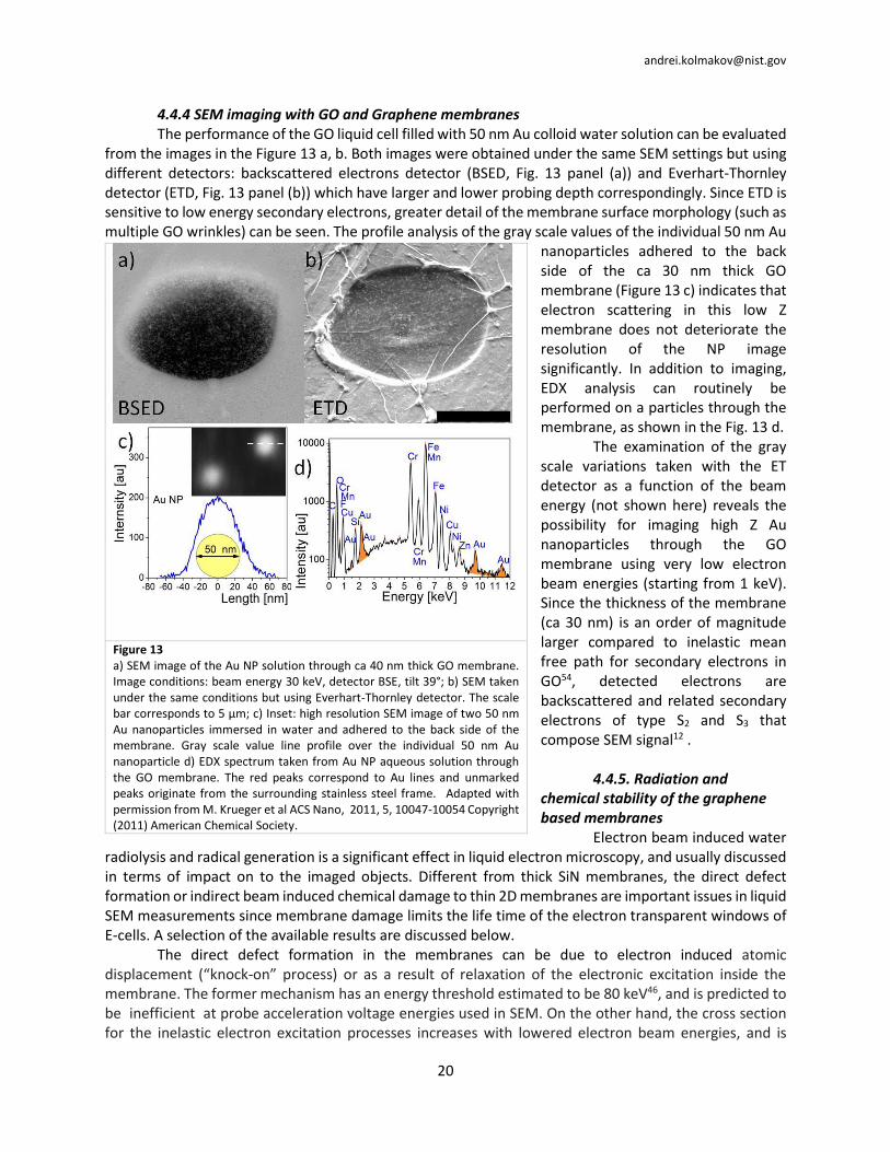
andreikolmakovnistgov
23
Disclaimer Official contribution of the National Institute of Standards and Technology not subject to copyright in the United States Acknowledgements AK thanks his SIUC students Shannon Berg Mark Krueger Joshua Cothren Joshua Stoll and Alexander Yulaev whose work became the base of this chapter The technical discussions with Christopher Brown Alex Liddle Dr Renu Sharma and Nikolai Zhitentev (all at NIST) are greatly appreciated References 1 G D Danilatos Inst Phys Conf Ser 1990 455-458 2 G D Dantilatos US Patent 4596928 1986 3 A Bogner G Thollet D Basset P-H Jouneau and C Gauthier Ultramicroscopy 2005 104 290-
301 4 I Abrams and J McBain Journal of Applied Physics 1944 15 607-609 5 S Thiberge O Zik and E Moses Review of Scientific Instruments 2004 75 2280-2289 6 M Suga H Nishiyama Y Konyuba S Iwamatsu Y Watanabe C Yoshiura T Ueda and C Sato
Ultramicroscopy 2011 111 1650-1658 7 N Vidavsky S Addadi J Mahamid E Shimoni D Ben-Ezra M Shpigel S Weiner and L Addadi
Proceedings of the National Academy of Sciences 2014 111 39-44 8 Y Ominami S Kawanishi T Ushiki and S Ito Microscopy 2014 dfu107 9 E Jensen A Burrows and K Moslashlhave Microscopy and Microanalysis 2014 20 445-451 10 H Demers N Poirier‐Demers A R Couture D Joly M Guilmain N de Jonge and D Drouin
Scanning 2011 33 135-146 11 K Kanaya and S Okayama Journal of Physics D Applied Physics 1972 5 43 12 J Goldstein D Newbury D Joy C Lyman P Echlin E Lifshin L Sawyer and J Michael 2003 13 R Egerton P Li and M Malac Micron 2004 35 399-409 14 D A Fischer D H Alsem B Simon T Prozorov and N Salmon Microscopy and Microanalysis
2013 19 476-477 15 V Behar O Gileadi Y Karni Y Kliger A Nechushtan D Sprinzak and O Zik US patent 7230242
B2 2007 16 S Thiberge A Nechushtan D Sprinzak O Gileadi V Behar O Zik Y Chowers S Michaeli J
Schlessinger and E Moses Proceedings of the National Academy of Sciences of the United States of America 2004 101 3346-3351
17 G Venkiteela and Z H Sun Cement amp Concrete Composites 2010 32 211-218 18 K Tiede S P Tear H David and A B A Boxall Water Research 2009 43 3335-3343 19 B G Mathapa and V N Paunov Physical Chemistry Chemical Physics 2013 15 17903-17914 20 C Lorenz K Tiede S Tear A Boxall N von Goetz and K Hungerbuhler International Journal of
Occupational and Environmental Health 2010 16 406-428 21 D C Joy and C S Joy Journal of Microscopy-Oxford 2006 221 84-88 22 A K F Dyab and V N Paunov Soft Matter 2010 6 2613-2615 23 O Cohen R Beery S Levit J Ilany I Schwartz M Shabtai D Anaby D Cohen R Alfici A
Czerniak and A Karasik Thyroid 2006 16 997-1001 24 N Kolmakova and A Kolmakov The Journal of Physical Chemistry C 2010 114 17233-17237 25 C Wei W Y Lin Z Zainal N E Williams K Zhu A P Kruzic R L Smith and K Rajeshwar
Environmental science amp technology 1994 28 934-938 26 J L Giocondi and G S Rohrer Topics in catalysis 2008 49 18-23
andreikolmakovnistgov
24
27 J M Herrmann Catalysis Today 1999 53 115-129 28 J Geisler-Lee Q Wang Y Yao W Zhang M Geisler K Li Y Huang Y Chen A Kolmakov and X
Ma Nanotoxicology 2012 7 323-337 29 N M Schneider M M Norton B J Mendel J M Grogan F M Ross and H H Bau The Journal
of Physical Chemistry C 2014 118 22373-22382 30 E U Donev and J T Hastings Nano letters 2009 9 2715-2718 31 A Al-Asadi J Zhang J Li R A Potyrailo and A Kolmakov arXiv preprint arXiv150100762
2015 32 C Monat P Domachuk and B Eggleton Nature photonics 2007 1 106-114 33 D Erickson D Sinton and D Psaltis Nature Photonics 2011 5 583-590 34 R A Potyrailo H Ghiradella A Vertiatchikh K Dovidenko J R Cournoyer and E Olson Nature
Photonics 2007 1 123-128 35 R A Potyrailo T A Starkey P Vukusic H Ghiradella M Vasudev T Bunning R R Naik Z
Tang M Larsen and T Deng Proceedings of the National Academy of Sciences 2013 110 15567-15572
36 R R Unocic X-G Sun R L Sacci L A Adamczyk D H Alsem S Dai N J Dudney and K L More Microscopy and Microanalysis 2014 20 1029-1037
37 K Klein I Anderson and N De Jonge Journal of microscopy 2011 242 117-123 38 K Moslashlhave C Kallesoslashe C Wen F Ross T Booth T Kjoslashller Nellemann E Jensen C Elkjaeligr J
Rasmussen and P Jensen Microscopy and Microanalysis 2010 16 322-323 39 J E Cothren Thesis Master of Science Southern Illinois University Carbondale 2011 40 Y Liu Master of Science Southern Illinois University at Carbondale 2013 41 S Ueda Y Kobayashi S Koizumi and Y Tsutsumi Microscopy 2014 dfu100 42 J C Meyer A K Geim M Katsnelson K Novoselov T Booth and S Roth Nature 2007 446
60-63 43 N R Wilson P A Pandey R Beanland R J Young I A Kinloch L Gong Z Liu K Suenaga J P
Rourke and S J York ACS nano 2009 3 2547-2556 44 C Lee X Wei J W Kysar and J Hone science 2008 321 385-388 45 I Muumlllerovaacute M Hovorka and L Frank Ultramicroscopy 2012 119 78-81 46 J C Meyer F Eder S Kurasch V Skakalova J Kotakoski H J Park S Roth A Chuvilin S
Eyhusen and G Benner Physical review letters 2012 108 196102 47 J C Meyer C O Girit M Crommie and A Zettl Nature 2008 454 319-322 48 R S Pantelic J C Meyer U Kaiser and H Stahlberg Solid State Communications 2012 152
1375-1382 49 J Mutus L Livadaru J Robinson R Urban M Salomons M Cloutier and R Wolkow New
Journal of Physics 2011 13 063011 50 J-N Longchamp C Escher T Latychevskaia and H-W Fink Ultramicroscopy 2014 51 L Frank E Mikmekovaacute I Muumlllerovaacute and M Lejeune Applied Physics Letters 2015 106 013117 52 A Jablonski and C Powell Journal of Vacuum Science amp Technology A Vacuum Surfaces and
Films 2009 27 253-261 53 S Tanuma C Powell and D Penn Surface and Interface Analysis 2011 43 689-713 54 A Kolmakov D A Dikin L J Cote J X Huang M K Abyaneh M Amati L Gregoratti S
Gunther and M Kiskinova Nature Nanotechnology 2011 6 651-657 55 J Kraus R Reichelt S Guenther L Gregoratti M Amati M Kiskinova A Yulaev I Vlassiokiv
and A Kolmakov Nanoscale 2014 56 M Xu D Fujita J Gao and N Hanagata Acs Nano 2010 4 2937-2945 57 V Kochat A N Pal E Sneha A Sampathkumar A Gairola S Shivashankar S Raghavan and A
Ghosh Journal of Applied Physics 2011 110 014315
andreikolmakovnistgov
25
58 M Krueger S Berg D Stone E Strelcov D A Dikin J Kim L J Cote J X Huang and A Kolmakov Acs Nano 2011 5 10047-10054
59 S Park and R S Ruoff Nature nanotechnology 2009 4 217-224 60 D Li M B Muumlller S Gilje R B Kaner and G G Wallace Nature nanotechnology 2008 3 101-
105 61 L J Cote J Kim V C Tung J Luo F Kim and J Huang Pure and Applied Chemistry 2010 83
95-110 62 D A Dikin S Stankovich E J Zimney R D Piner G H Dommett G Evmenenko S T Nguyen
and R S Ruoff Nature 2007 448 457-460 63 S Park K-S Lee G Bozoklu W Cai S T Nguyen and R S Ruoff ACS nano 2008 2 572-578 64 R Nair H Wu P Jayaram I Grigorieva and A Geim Science 2012 335 442-444 65 H W Kim H W Yoon S-M Yoon B M Yoo B K Ahn Y H Cho H J Shin H Yang U Paik and
S Kwon Science 2013 342 91-95 66 R Joshi P Carbone F Wang V Kravets Y Su I Grigorieva H Wu A Geim and R Nair Science
2014 343 752-754 67 J S Bunch S S Verbridge J S Alden A M van der Zande J M Parpia H G Craighead and P
L McEuen Nano letters 2008 8 2458-2462 68 J Kang D Shin S Bae and B H Hong Nanoscale 2012 4 5527-5537 69 F Bonaccorso A Lombardo T Hasan Z Sun L Colombo and A C Ferrari Materials Today
2012 15 564-589 70 Y-C Lin C-C Lu C-H Yeh C Jin K Suenaga and P-W Chiu Nano letters 2011 12 414-419 71 J W Suk A Kitt C W Magnuson Y Hao S Ahmed J An A K Swan B B Goldberg and R S
Ruoff ACS nano 2011 5 6916-6924 72 A A Balandin S Ghosh W Bao I Calizo D Teweldebrhan F Miao and C N Lau Nano letters
2008 8 902-907 73 L J Cote R Cruz-Silva and J Huang Journal of the American Chemical Society 2009 131
11027-11032 74 S Gilje S Dubin A Badakhshan J Farrar S Danczyk and R B Kaner Advanced Materials 2010
22 419-423 75 P Kumar K Subrahmanyam and C Rao Materials Express 2011 1 252-256 76 G Liu D Teweldebrhan and A A Balandin Nanotechnology IEEE Transactions on 2011 10
865-870 77 I Childres L A Jauregui M Foxe J Tian R Jalilian I Jovanovic and Y P Chen Applied Physics
Letters 2010 97 173109 78 L Tao C Qiu F Yu H Yang M Chen G Wang and L Sun The Journal of Physical Chemistry C
2013 117 10079-10085 79 X Feng S Maier and M Salmeron Journal of the American Chemical Society 2012 134 5662-
5668 80 M Baraket S Walton Z Wei E Lock J Robinson and P Sheehan Carbon 2010 48 3382-3390 81 C Royall B Thiel and A Donald Journal of Microscopy 2001 204 185-195 82 J D Stoll and A Kolmakov Nanotechnology 2012 23
andreikolmakovnistgov
24
27 J M Herrmann Catalysis Today 1999 53 115-129 28 J Geisler-Lee Q Wang Y Yao W Zhang M Geisler K Li Y Huang Y Chen A Kolmakov and X
Ma Nanotoxicology 2012 7 323-337 29 N M Schneider M M Norton B J Mendel J M Grogan F M Ross and H H Bau The Journal
of Physical Chemistry C 2014 118 22373-22382 30 E U Donev and J T Hastings Nano letters 2009 9 2715-2718 31 A Al-Asadi J Zhang J Li R A Potyrailo and A Kolmakov arXiv preprint arXiv150100762
2015 32 C Monat P Domachuk and B Eggleton Nature photonics 2007 1 106-114 33 D Erickson D Sinton and D Psaltis Nature Photonics 2011 5 583-590 34 R A Potyrailo H Ghiradella A Vertiatchikh K Dovidenko J R Cournoyer and E Olson Nature
Photonics 2007 1 123-128 35 R A Potyrailo T A Starkey P Vukusic H Ghiradella M Vasudev T Bunning R R Naik Z
Tang M Larsen and T Deng Proceedings of the National Academy of Sciences 2013 110 15567-15572
36 R R Unocic X-G Sun R L Sacci L A Adamczyk D H Alsem S Dai N J Dudney and K L More Microscopy and Microanalysis 2014 20 1029-1037
37 K Klein I Anderson and N De Jonge Journal of microscopy 2011 242 117-123 38 K Moslashlhave C Kallesoslashe C Wen F Ross T Booth T Kjoslashller Nellemann E Jensen C Elkjaeligr J
Rasmussen and P Jensen Microscopy and Microanalysis 2010 16 322-323 39 J E Cothren Thesis Master of Science Southern Illinois University Carbondale 2011 40 Y Liu Master of Science Southern Illinois University at Carbondale 2013 41 S Ueda Y Kobayashi S Koizumi and Y Tsutsumi Microscopy 2014 dfu100 42 J C Meyer A K Geim M Katsnelson K Novoselov T Booth and S Roth Nature 2007 446
60-63 43 N R Wilson P A Pandey R Beanland R J Young I A Kinloch L Gong Z Liu K Suenaga J P
Rourke and S J York ACS nano 2009 3 2547-2556 44 C Lee X Wei J W Kysar and J Hone science 2008 321 385-388 45 I Muumlllerovaacute M Hovorka and L Frank Ultramicroscopy 2012 119 78-81 46 J C Meyer F Eder S Kurasch V Skakalova J Kotakoski H J Park S Roth A Chuvilin S
Eyhusen and G Benner Physical review letters 2012 108 196102 47 J C Meyer C O Girit M Crommie and A Zettl Nature 2008 454 319-322 48 R S Pantelic J C Meyer U Kaiser and H Stahlberg Solid State Communications 2012 152
1375-1382 49 J Mutus L Livadaru J Robinson R Urban M Salomons M Cloutier and R Wolkow New
Journal of Physics 2011 13 063011 50 J-N Longchamp C Escher T Latychevskaia and H-W Fink Ultramicroscopy 2014 51 L Frank E Mikmekovaacute I Muumlllerovaacute and M Lejeune Applied Physics Letters 2015 106 013117 52 A Jablonski and C Powell Journal of Vacuum Science amp Technology A Vacuum Surfaces and
Films 2009 27 253-261 53 S Tanuma C Powell and D Penn Surface and Interface Analysis 2011 43 689-713 54 A Kolmakov D A Dikin L J Cote J X Huang M K Abyaneh M Amati L Gregoratti S
Gunther and M Kiskinova Nature Nanotechnology 2011 6 651-657 55 J Kraus R Reichelt S Guenther L Gregoratti M Amati M Kiskinova A Yulaev I Vlassiokiv
and A Kolmakov Nanoscale 2014 56 M Xu D Fujita J Gao and N Hanagata Acs Nano 2010 4 2937-2945 57 V Kochat A N Pal E Sneha A Sampathkumar A Gairola S Shivashankar S Raghavan and A
Ghosh Journal of Applied Physics 2011 110 014315
andreikolmakovnistgov
25
58 M Krueger S Berg D Stone E Strelcov D A Dikin J Kim L J Cote J X Huang and A Kolmakov Acs Nano 2011 5 10047-10054
59 S Park and R S Ruoff Nature nanotechnology 2009 4 217-224 60 D Li M B Muumlller S Gilje R B Kaner and G G Wallace Nature nanotechnology 2008 3 101-
105 61 L J Cote J Kim V C Tung J Luo F Kim and J Huang Pure and Applied Chemistry 2010 83
95-110 62 D A Dikin S Stankovich E J Zimney R D Piner G H Dommett G Evmenenko S T Nguyen
and R S Ruoff Nature 2007 448 457-460 63 S Park K-S Lee G Bozoklu W Cai S T Nguyen and R S Ruoff ACS nano 2008 2 572-578 64 R Nair H Wu P Jayaram I Grigorieva and A Geim Science 2012 335 442-444 65 H W Kim H W Yoon S-M Yoon B M Yoo B K Ahn Y H Cho H J Shin H Yang U Paik and
S Kwon Science 2013 342 91-95 66 R Joshi P Carbone F Wang V Kravets Y Su I Grigorieva H Wu A Geim and R Nair Science
2014 343 752-754 67 J S Bunch S S Verbridge J S Alden A M van der Zande J M Parpia H G Craighead and P
L McEuen Nano letters 2008 8 2458-2462 68 J Kang D Shin S Bae and B H Hong Nanoscale 2012 4 5527-5537 69 F Bonaccorso A Lombardo T Hasan Z Sun L Colombo and A C Ferrari Materials Today
2012 15 564-589 70 Y-C Lin C-C Lu C-H Yeh C Jin K Suenaga and P-W Chiu Nano letters 2011 12 414-419 71 J W Suk A Kitt C W Magnuson Y Hao S Ahmed J An A K Swan B B Goldberg and R S
Ruoff ACS nano 2011 5 6916-6924 72 A A Balandin S Ghosh W Bao I Calizo D Teweldebrhan F Miao and C N Lau Nano letters
2008 8 902-907 73 L J Cote R Cruz-Silva and J Huang Journal of the American Chemical Society 2009 131
11027-11032 74 S Gilje S Dubin A Badakhshan J Farrar S Danczyk and R B Kaner Advanced Materials 2010
22 419-423 75 P Kumar K Subrahmanyam and C Rao Materials Express 2011 1 252-256 76 G Liu D Teweldebrhan and A A Balandin Nanotechnology IEEE Transactions on 2011 10
865-870 77 I Childres L A Jauregui M Foxe J Tian R Jalilian I Jovanovic and Y P Chen Applied Physics
Letters 2010 97 173109 78 L Tao C Qiu F Yu H Yang M Chen G Wang and L Sun The Journal of Physical Chemistry C
2013 117 10079-10085 79 X Feng S Maier and M Salmeron Journal of the American Chemical Society 2012 134 5662-
5668 80 M Baraket S Walton Z Wei E Lock J Robinson and P Sheehan Carbon 2010 48 3382-3390 81 C Royall B Thiel and A Donald Journal of Microscopy 2001 204 185-195 82 J D Stoll and A Kolmakov Nanotechnology 2012 23