Embed Size (px)
DESCRIPTION
Crystal Defect
Citation preview
Chapter 4: Crystal Defects – Imperfection
1
Strength of Materials
• Based on the bond strength most materials should be much stronger than they are
• From Chapter one: the strength for an ionic bond should be about 106 psi
• More typical strength is 40*103 psi• Why do we have three orders of magnitude
difference?
2
Crystalline Imperfections• Real materials are never perfect and contain various types of
imperfections, which affect many of their properties.
• Some properties affected by imperfections include tensile and ultimate strengths, thermal conductivity, electrical conductivity, photonic generation and conductivity, magnetic properties, etc. For example, Point defects ↑ ionic conductivity, but grain boundaries ↓ ionic conductivity
• Crystal lattice imperfections are classified according to their geometry and shape.
• Point defects are zero dimension• Line defects are one dimensional• Planar defects are two dimensional and comprise of free surfaces
and grain boundaries
3
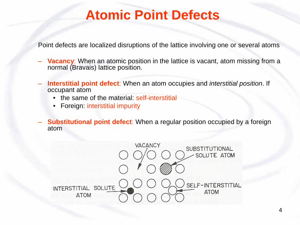
Atomic Point Defects
Point defects are localized disruptions of the lattice involving one or several atoms
– Vacancy: When an atomic position in the lattice is vacant, atom missing from a normal (Bravais) lattice position.
– Interstitial point defect: When an atom occupies and interstitial position. If occupant atom
• the same of the material: self-interstitial• Foreign: interstitial impurity
– Substitutional point defect: When a regular position occupied by a foreign atom
4
Chemical Impurity- foreign atom• Size usually dictates the site and if
– substitutional– Interstitial
• May be intentional or unintentional– Examples: carbon added in small amounts to iron
makes steel, which is stronger than pure iron. Boron added to silicon change its electrical properties.
• If foreign atoms are incorporated into the crystal (matrix) solid solutions (general) alloy (deliberate mixtures of metals)
5
Chemical Impurity - Solid Solution
• Solid solutions are made of a host (the solvent or matrix) which dissolves the minor component (solute). The ability to dissolve is called solubility.– Solvent: in an alloy, the element or compound present in
greater amount– Solute: in an alloy, the element or compound present in
lesser amount– Solid Solution:
• "homogeneous• "maintain crystal structure• "contain randomly dispersed impurities (substitutional or
interstitial)
Example: sterling silver is 92.5% silver – 7.5% copper alloy. Stronger than pure silver. 6
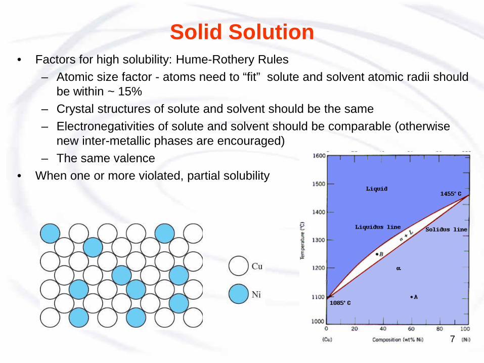
Solid Solution• Factors for high solubility: Hume-Rothery Rules
– Atomic size factor - atoms need to “fit” solute and solvent atomic radii should be within ~ 15%
– Crystal structures of solute and solvent should be the same – Electronegativities of solute and solvent should be comparable (otherwise
new inter-metallic phases are encouraged) – The same valence
• When one or more violated, partial solubility
7
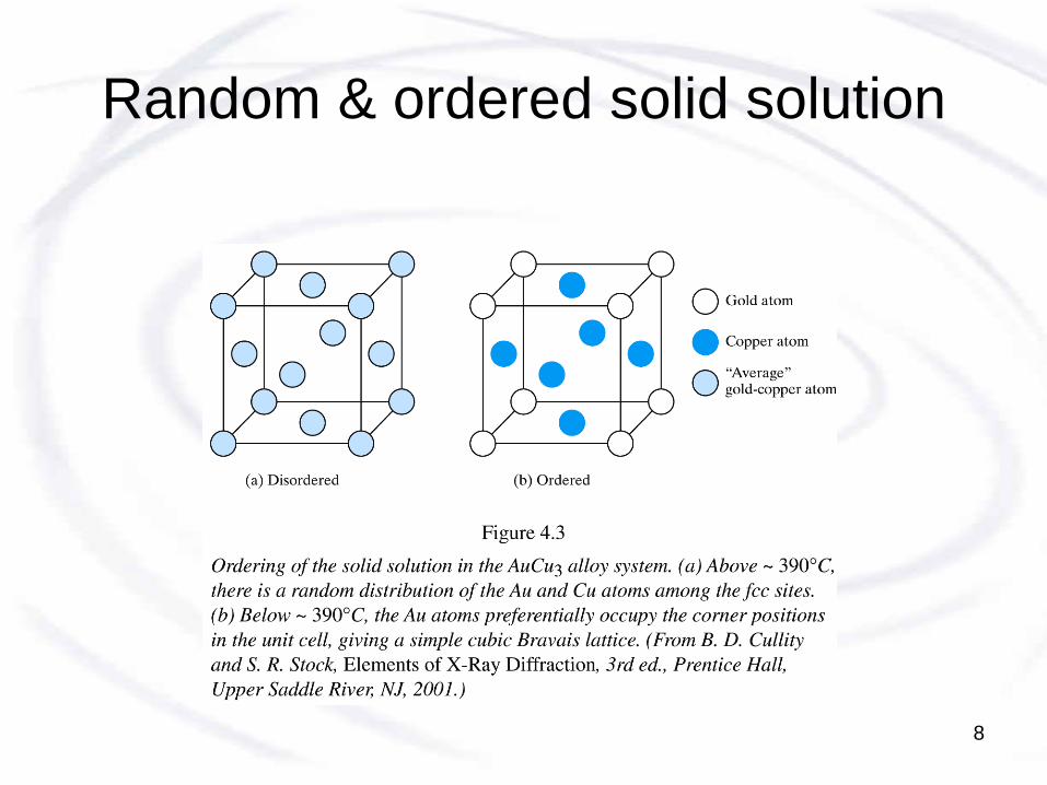
Random & ordered solid solution
8
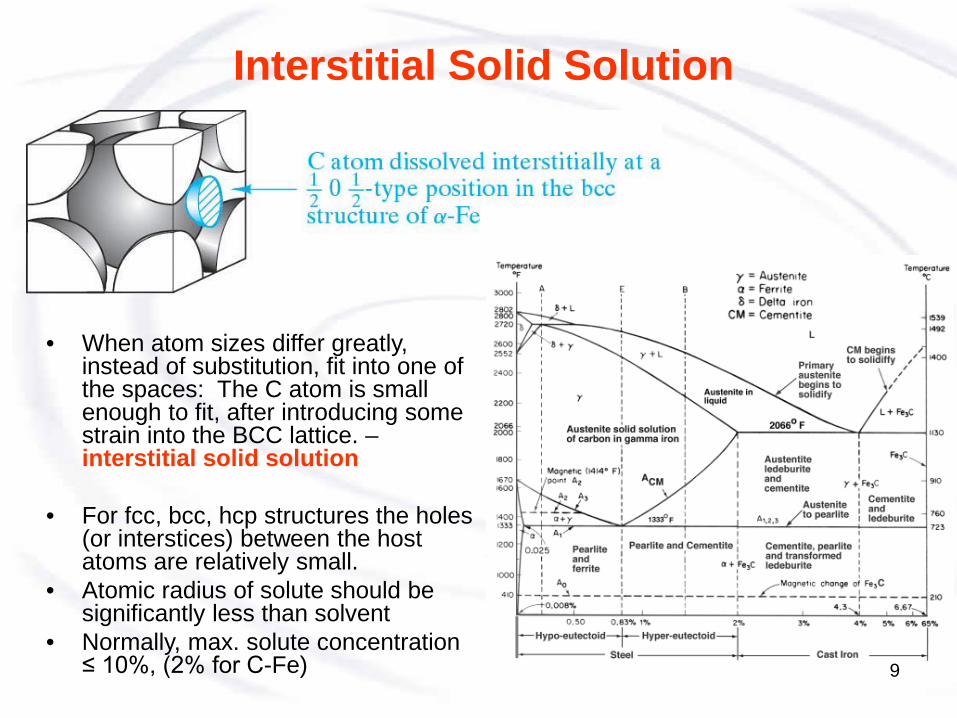
Interstitial Solid Solution
• When atom sizes differ greatly, instead of substitution, fit into one of the spaces: The C atom is small enough to fit, after introducing some strain into the BCC lattice. –interstitial solid solution
• For fcc, bcc, hcp structures the holes (or interstices) between the host atoms are relatively small.
• Atomic radius of solute should be significantly less than solvent
• Normally, max. solute concentration ≤ 10%, (2% for C-Fe) 9
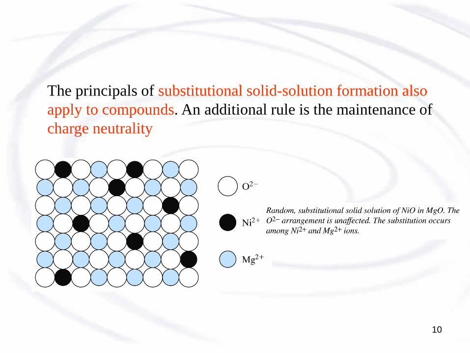
The principals of substitutional solid-solution formation also apply to compounds. An additional rule is the maintenance of charge neutrality
10
Vacancies• Usually introduced during solidification, at high T• The vacancy concentration in pure elements is very
low at low temperatures.– The probability that an atomic site is vacancy ~ 10-6 at low T– The probability that an atomic site is vacancy ~ 10-3 at
melting T• can affect physical and electronic structures around
them →influence properties like color, conductivity• they play a critical role in diffusion: control the self
diffusion and substitutional diffusion rates• Movements of atoms coupled with movements of
vacancies
11
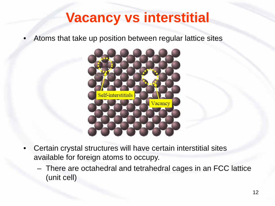
Vacancy vs interstitial• Atoms that take up position between regular lattice sites
• Certain crystal structures will have certain interstitial sites available for foreign atoms to occupy.– There are octahedral and tetrahedral cages in an FCC lattice
(unit cell)
12
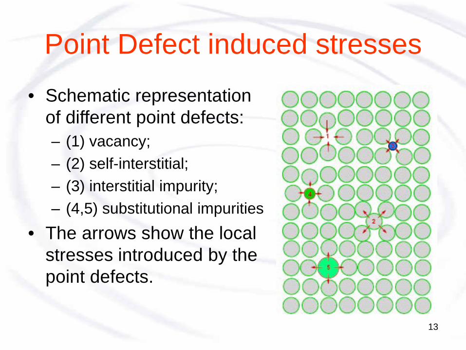
Point Defect induced stresses
• Schematic representation of different point defects:– (1) vacancy;– (2) self-interstitial;– (3) interstitial impurity;– (4,5) substitutional impurities
• The arrows show the local stresses introduced by the point defects.
13
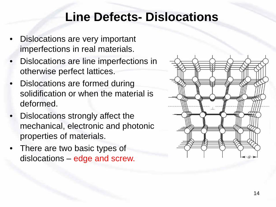
Line Defects- Dislocations• Dislocations are very important
imperfections in real materials.• Dislocations are line imperfections in
otherwise perfect lattices.• Dislocations are formed during
solidification or when the material is deformed.
• Dislocations strongly affect the mechanical, electronic and photonic properties of materials.
• There are two basic types of dislocations – edge and screw.
14
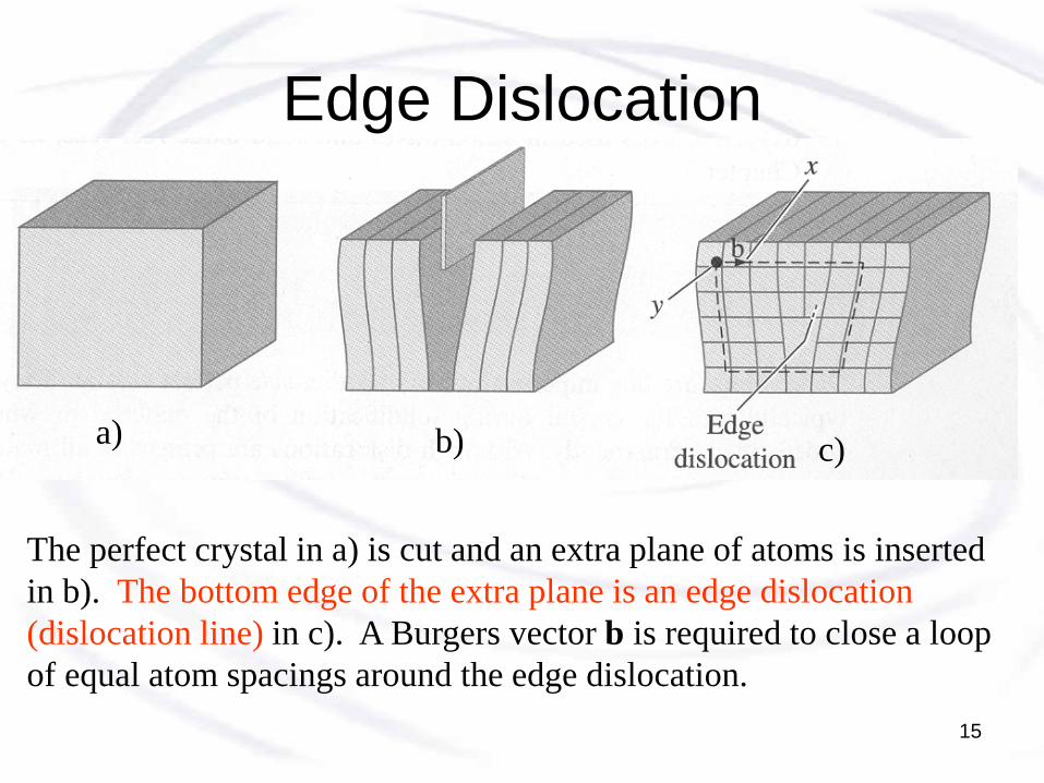
The perfect crystal in a) is cut and an extra plane of atoms is inserted in b). The bottom edge of the extra plane is an edge dislocation (dislocation line) in c). A Burgers vector b is required to close a loop of equal atom spacings around the edge dislocation.
a) b) c)
Edge Dislocation
15
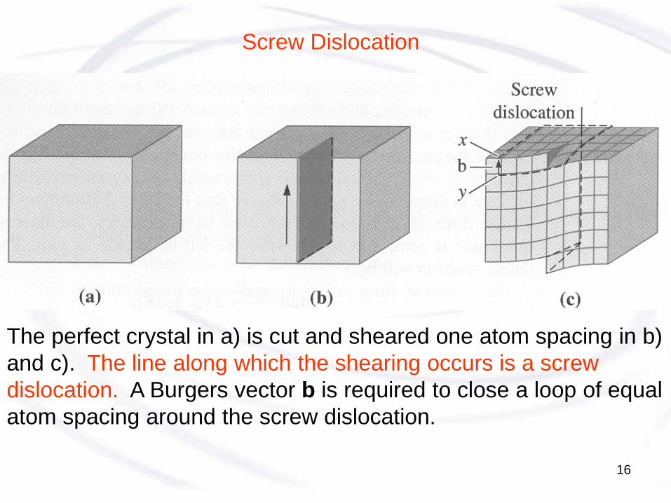
The perfect crystal in a) is cut and sheared one atom spacing in b) and c). The line along which the shearing occurs is a screw dislocation. A Burgers vector b is required to close a loop of equal atom spacing around the screw dislocation.
Screw Dislocation
16
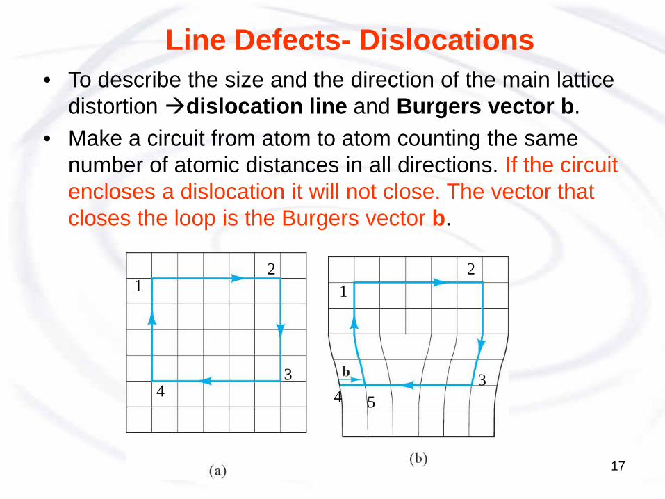
Line Defects- Dislocations• To describe the size and the direction of the main lattice
distortion dislocation line and Burgers vector b. • Make a circuit from atom to atom counting the same
number of atomic distances in all directions. If the circuit encloses a dislocation it will not close. The vector that closes the loop is the Burgers vector b.
12
34
12
34 5
17
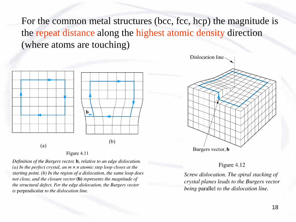
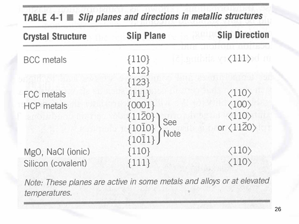
For the common metal structures (bcc, fcc, hcp) the magnitude is the repeat distance along the highest atomic density direction (where atoms are touching)
18
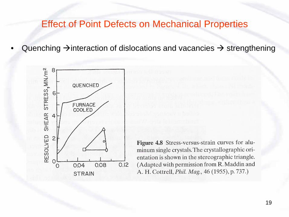
Effect of Point Defects on Mechanical Properties
• Quenching interaction of dislocations and vacancies strengthening
19
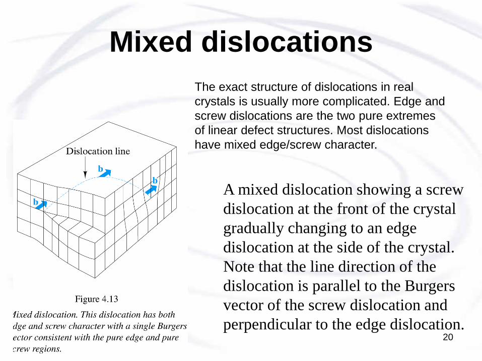
Mixed dislocations
A mixed dislocation showing a screw dislocation at the front of the crystal gradually changing to an edge dislocation at the side of the crystal. Note that the line direction of the dislocation is parallel to the Burgers vector of the screw dislocation and perpendicular to the edge dislocation.
The exact structure of dislocations in real crystals is usually more complicated. Edge and screw dislocations are the two pure extremes of linear defect structures. Most dislocations have mixed edge/screw character.
20
Control of Dislocations• Control of dislocations allow us to manipulate mechanical
properties and understand their temperature dependence.• When a shear force acting in the direction of the
Burger’s vector is applied to a crystal containing a dislocation, the dislocation can move by breaking bonds between the atoms in one plane.
• By this process, the dislocation moves through the crystal to produce a step on the exterior of the crystal.
• The process by which the dislocation moves and causes a solid to deform is called slip.
21
Dislocation Slip• Dislocations move more readily in some crystal planes and
directions than in others as we will see.• The slip direction of an edge dislocation is in the direction of the
Burger’s vector.• A slip plane is defined by the direction of the Burger’s vector
and the line direction of the dislocation– The line direction of a screw dislocation is in the same
direction as its Burger’s vector.– An edge dislocation has its Burger’s vector perpendicular to
the line direction of a dislocation– A dislocation having a line direction not parallel or
perpendicular to the Burger’s vector is considered a mixeddislocation.
22
• During slip the dislocation moves from one set of surroundings to another identical set.
• The least amount of energy expenditure requires movement in directions in which the repeat distance is shortest, i.e., close-packed directions.
• Slip planes tend to be those planes with a high planar packing, i.e., close-packed planes.
• Slip reduces strength but increase ductility in materials.
Dislocation Slip
23
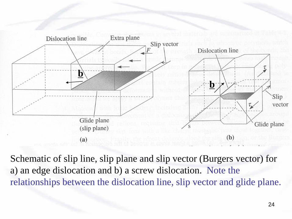
Schematic of slip line, slip plane and slip vector (Burgers vector) for a) an edge dislocation and b) a screw dislocation. Note the relationships between the dislocation line, slip vector and glide plane.
bb
24
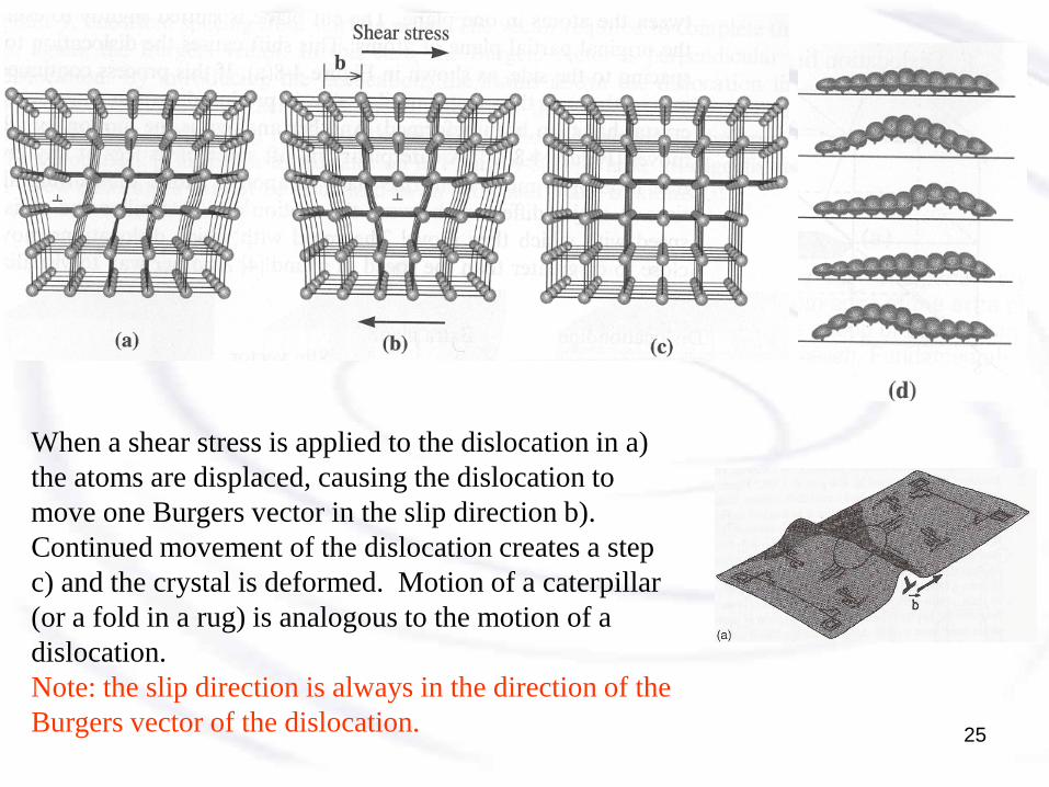
When a shear stress is applied to the dislocation in a) the atoms are displaced, causing the dislocation to move one Burgers vector in the slip direction b). Continued movement of the dislocation creates a step c) and the crystal is deformed. Motion of a caterpillar (or a fold in a rug) is analogous to the motion of a dislocation. Note: the slip direction is always in the direction of the Burgers vector of the dislocation. 25
26
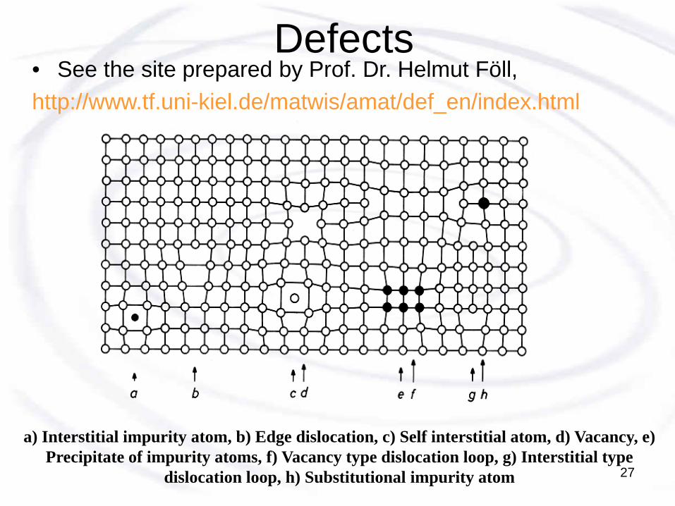
Defects• See the site prepared by Prof. Dr. Helmut Föll,http://www.tf.uni-kiel.de/matwis/amat/def_en/index.html
a) Interstitial impurity atom, b) Edge dislocation, c) Self interstitial atom, d) Vacancy, e) Precipitate of impurity atoms, f) Vacancy type dislocation loop, g) Interstitial type
dislocation loop, h) Substitutional impurity atom 27
Observing Dislocations• We can view dislocations indirectly by etching the
surface of a material. Where the dislocation intersects the surface, it is preferentially etched creating a pit, which can easily be seen optically.
• Using a transmission electron microscope, we can see the strain contrast that a dislocation makes as it passes through a crystal, or at the atomic level we can see the displacement of atomic columns due to the presence of a dislocation.
28
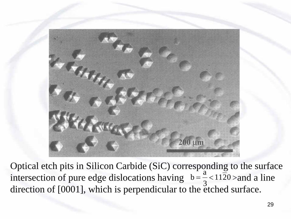
Optical etch pits in Silicon Carbide (SiC) corresponding to the surface intersection of pure edge dislocations having and a line direction of [0001], which is perpendicular to the etched surface.
><= 02113ab
29
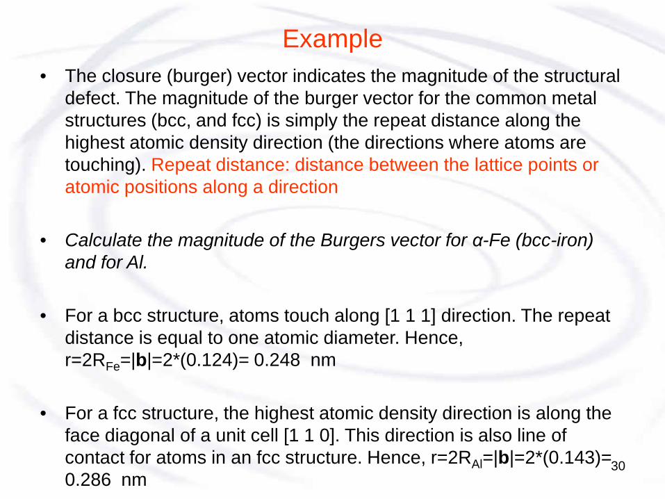
Example• The closure (burger) vector indicates the magnitude of the structural
defect. The magnitude of the burger vector for the common metal structures (bcc, and fcc) is simply the repeat distance along the highest atomic density direction (the directions where atoms are touching). Repeat distance: distance between the lattice points or atomic positions along a direction
• Calculate the magnitude of the Burgers vector for α-Fe (bcc-iron) and for Al.
• For a bcc structure, atoms touch along [1 1 1] direction. The repeat distance is equal to one atomic diameter. Hence, r=2RFe=|b|=2*(0.124)= 0.248 nm
• For a fcc structure, the highest atomic density direction is along the face diagonal of a unit cell [1 1 0]. This direction is also line of contact for atoms in an fcc structure. Hence, r=2RAl=|b|=2*(0.143)= 0.286 nm
30
Control of Slip Process – Strengthening Mechanisms
• We can control the strength of a material by controlling the number and type of imperfections in real materials.– These imperfection block the movement of dislocations making it
difficult for dislocation motion.• Five common mechanisms for increasing the strength of a material are:• Strain hardening• Solid solution strengthening• Grain refinement • Secondary phases• Dispersion hardening (age hardening)
31
Control of Slip Process – Strengthening Mechanisms
• 1) strain hardening, which increases the number of dislocations in the material by deforming the material. The extra dislocations block the motion of other dislocations.
• 2) solid solution strengthening, which adds point defects consisting of substitutional or interstitial atoms (alloying additions or impurities, i.e., foreign atoms). The strain around the foreign atoms blocks the motion of dislocations.
• 3) grain size strengthening (grain refinement), which reduces grain size where the grain boundaries block the motion of dislocations.
• 4) Secondary phases where some grains can have one type of atomic structure, eg., bcc, and other grains will have another type of atomic structure, eg., fcc. An example is α/β brass. Dislocations have difficulty passing from one type of grain to the other.
• 5) Dispersion hardening (age hardening) where small precipitates within grains are used to block the motion of dislocations.
32
Strengthening MechanismsThese five processes are used to increase the
strength of a material.From time to time during this course we will discuss
these five mechanisms in greater detail.
33
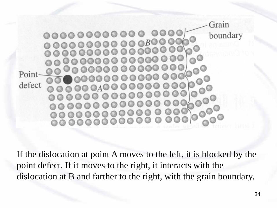
If the dislocation at point A moves to the left, it is blocked by the point defect. If it moves to the right, it interacts with the dislocation at B and farther to the right, with the grain boundary.
34
Planar defects – Grain Boundaries• Generally speaking, we deal with finite amount of (any)
material contained within some exterior boundarysurface.– Boundary surface itself a disruption of the atomic stacking
arrangement of the crystal a planar defect
• Interior boundaries– Aside from the electronics industry, most practical engineering
materials are polycrystalline– When crystals of different crystallographic orientations are
joined grain boundary
35
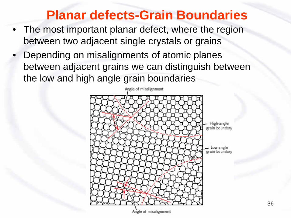
Planar defects-Grain Boundaries• The most important planar defect, where the region
between two adjacent single crystals or grains• Depending on misalignments of atomic planes
between adjacent grains we can distinguish between the low and high angle grain boundaries
36
Affect of Grain Size on Strength
• In a small grain, a dislocation gets to the boundary and stops – slip stops
• In a large grain, the dislocation can travel farther• Small grain size equates to more strength
37