Embed Size (px)
DESCRIPTION
c programming with example
Citation preview

Digital IC Design and ArchitectureDigital IC Design and Architecture
MOS TransistorMOS Transistor
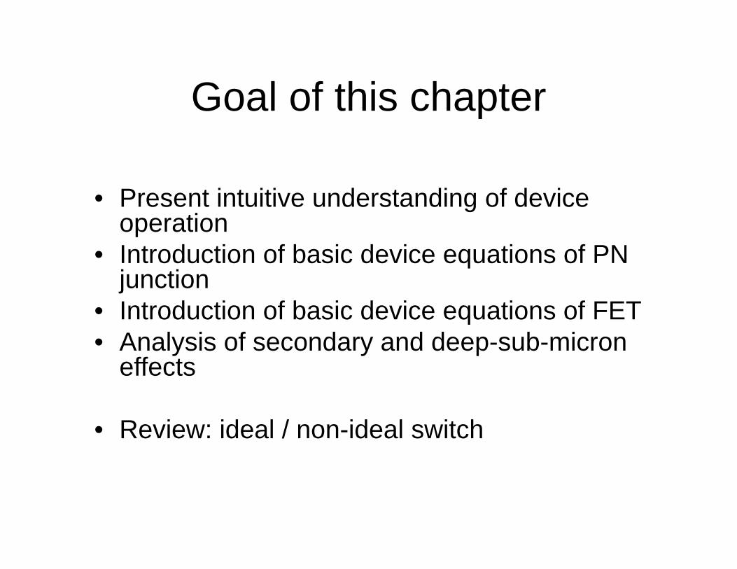
Goal of this chapterGoal of this chapter
• Present intuitive understanding of device operationI t d ti f b i d i ti f PN• Introduction of basic device equations of PN junction
• Introduction of basic device equations of FETq• Analysis of secondary and deep-sub-micron
effects
• Review: ideal / non-ideal switch

Properties of SiProperties of Si

Properties of Si
• covalent bonding in the Si• covalent bonding in the Si crystal, veiwed along a <100> direction
Energy band diagram of Si:Eg=1.1eV

Typical band structures at 0 Ky
A. Insulators have large band gaps which prevents electrons to “jump” from valence to conduction band. B. Semiconductors have smaller band gaps such that electrons can be thermally excited to the conduction band C. In metals, large number of electrons exist in the valence band.

Doping of Silicong
Energy band model and chemical bond model of dopants in semiconductors: (a) donation of electrons from donor level to conduction band; (b) acceptance of valence band electrons by an acceptor level, and the resulting creation of holes; (c) donor and acceptor atoms in the covalent bonding model of a Si crystal.
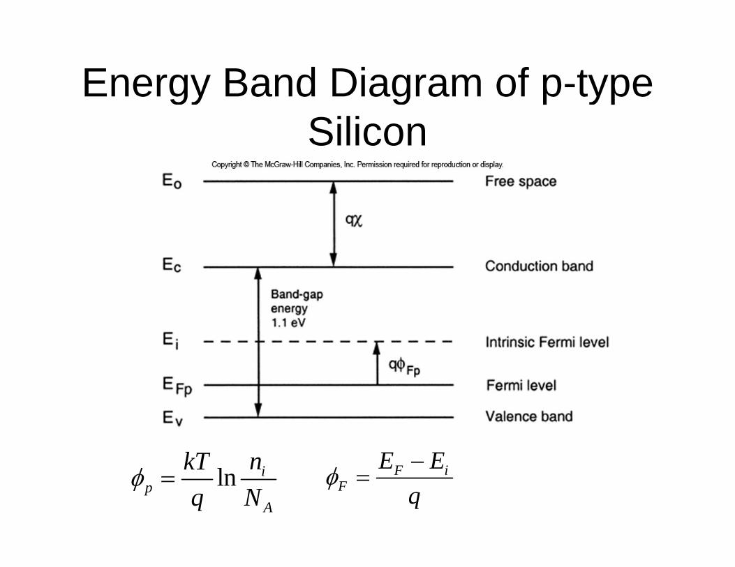
Energy Band Diagram of p-type gy g ySilicon
nkT E Eln i
pA
nkTq N
F iF
E Eq

Junction between two materials
Two materials in intimate contact at equilibrium. qNote: Since the net motion of electrons is zero, the equilibrium Fermi level must be constant throughout.

PN Junction: Energy Bandgy
0 2ln a d
i
N NkTVq n
1/22 V N N 2 ( )o a d
a d
V N NWq N N

PN Junction Under External Bias

MOSFET Energy MOSFET Energy B d DiB d DiBand DiagramBand Diagram

Two terminal MOS Structure

Energy Band Diagram of FETgy g
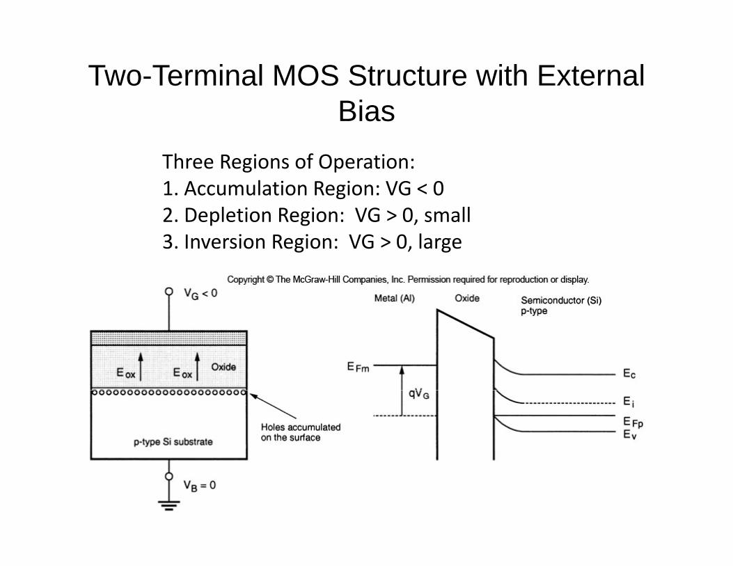
Two-Terminal MOS Structure with External BiBias
Three Regions of Operation:1. Accumulation Region: VG < 02. Depletion Region: VG > 0, small3. Inversion Region: VG > 0, large3. Inversion Region: VG > 0, large
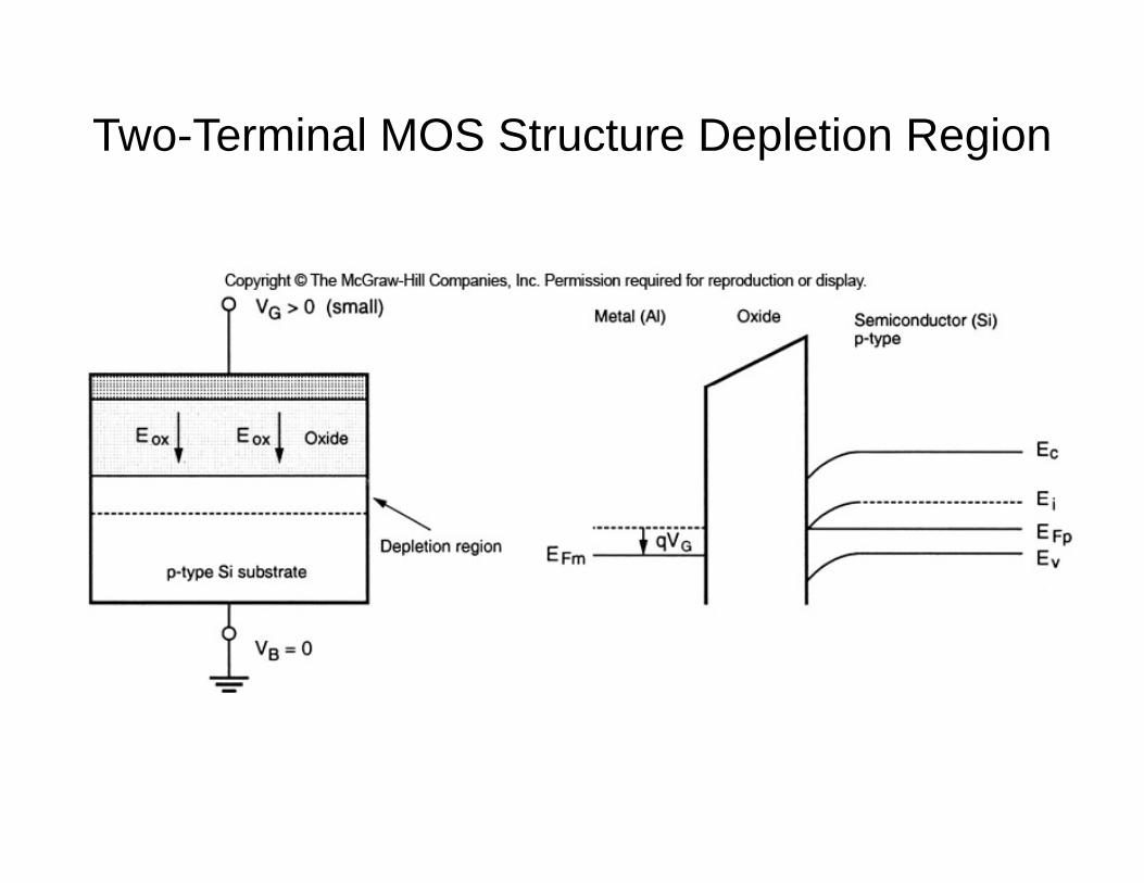
Two-Terminal MOS Structure Depletion Region

Two-Terminal MOS Structure Inversion Region

Two-Terminal MOS Structure Energy Band DiagramDiagram
Bending of the semiconductor bands at the onset of strong inversion: the surface potential fs is twice the value of fF in the neutral p material.

Two-Terminal MOS Structure Depletion Region

Two-Terminal MOS Structure Inversion Region


MOSFET IMOSFET I‐‐V V Ch t i tiCh t i tiCharacteristics Characteristics
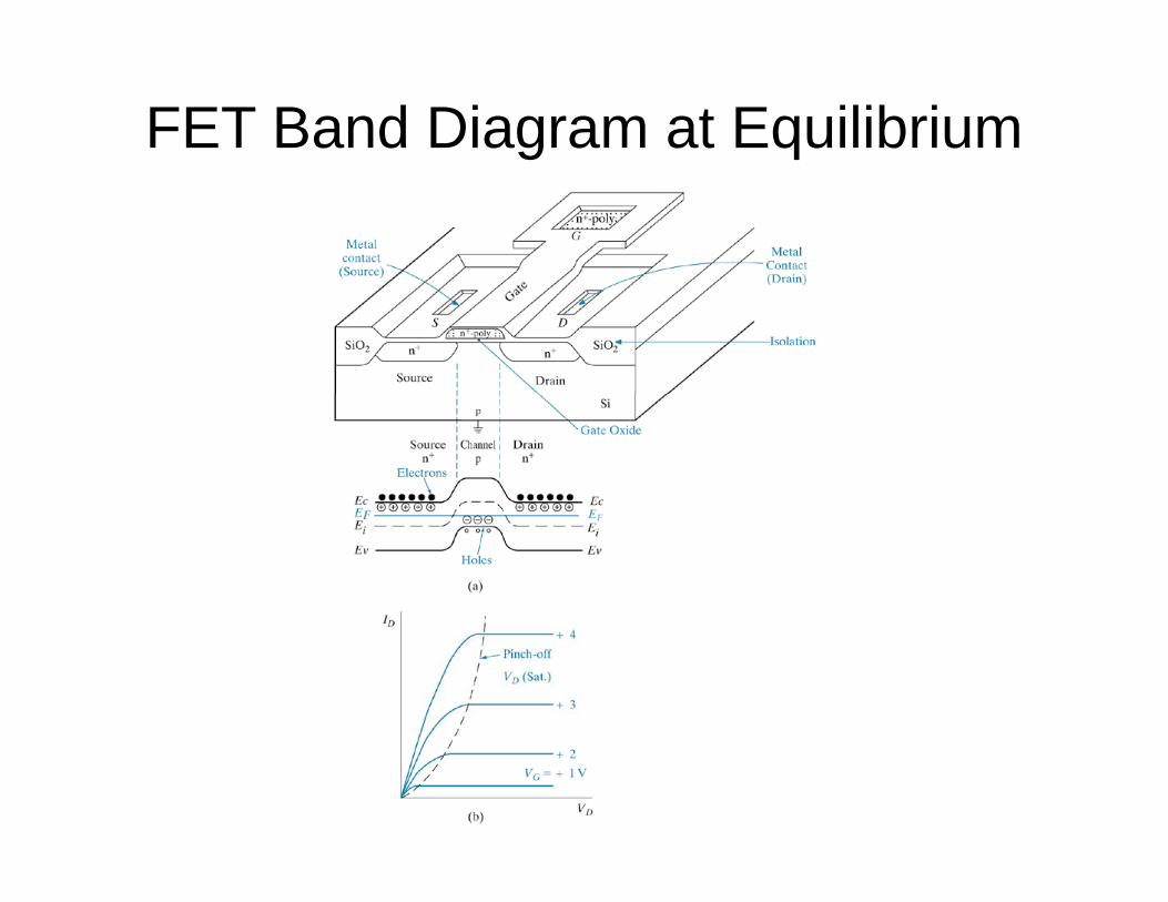
FET Band Diagram at Equilibrium

MOS Operation: A Qualitative View
n-channel MOSFET cross-sections under different operating conditions: (a) linear region for VG > VT and VD < (VG - VT); (b) onset of saturation at pinch-off, VG > VT and VD = (VG - VT); (c) strong saturation, VG > VT and VD > (VG - VT ).

Gradual Channel Approximation
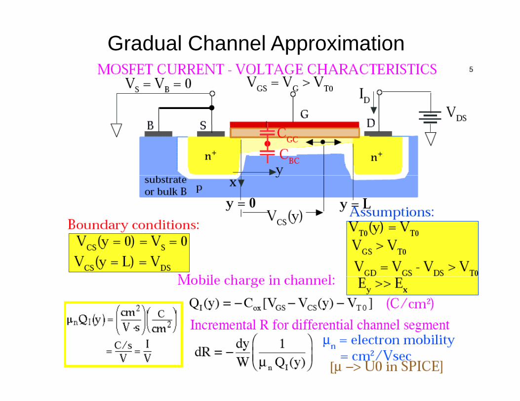
Gradual Channel Approximation

Gradual Channel Approximation
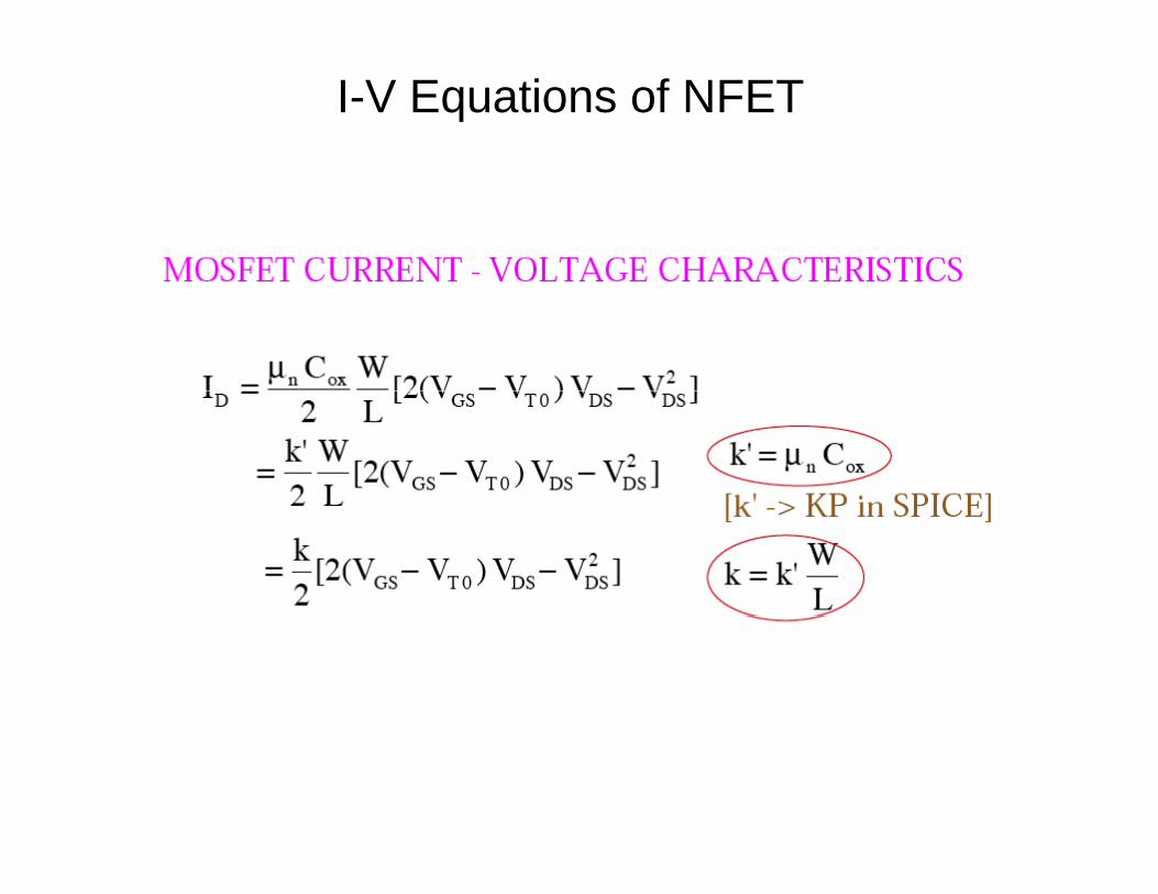
I-V Equations of NFET

I-V Equations of NFET

NFET in saturation region

NFET in saturation region: 2nd order effects

NFET in saturation region: complete

NFET equations

PMOS and NMOS equations


MOSFET ScalingMOSFET Scaling

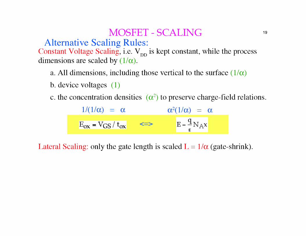

Scaling Effects

MOSFET MOSFET C itC itCapacitance Capacitance ModelsModelsModelsModels


MOSFET – Saturation RegionMOSFET Saturation Region

Capacitance Summary

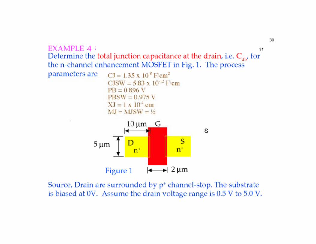
Drain/Source Capacitance

Drain/Source Capacitance

Depletion Region Capacitance

Depletion Region Capacitance

Depletion Region Capacitance