Embed Size (px)
Citation preview
Chapter 2Local Oxidation Using Dynamic Force Mode:Toward Higher Reliability and Efficiency
Hiromi Kuramochi and John A. Dagata
Abstract Local oxidation by scanning probe microscopy (SPM) is used extensivelyfor patterning nanostructures on metallic, insulating, and semiconducting thin filmsand substrates. Numerous possibilities for refining the process by controlling chargedensity within the oxide and shaping the water meniscus formed at the junction ofthe probe tip and substrate have been explored by a large number of researchersunder both contact mode (CM) and dynamic-force mode (DFM) conditions. Thisarticle addresses the question of whether or not the oxide growth rate and featuresize obtainable by each method arise from distinctly different kinetic processes orarise simply because charge buildup and dissipation evolve over different time scalesfor these two cases. We report simultaneous oxide-volume and current-flow mea-surements for exposures performed by CM and DFM and then go on to discuss thepractical realization of enhanced reliability and energy efficiency made possible bya better understanding of the relation between oxidation time and ionic diffusionusing DFM.
Keywords Meniscus formation · Oxidation time · Probe speed
2.1 Introduction
Local oxidation by scanning probe microscopy (SPM) [1] is a method for generat-ing deliberate nanoscale patterns on a wide variety of substrates [See References 2–4for reviews]. The fundamental principle of local oxidation is quite straightforward:A voltage applied between a conductive SPM tip and (positively biased) substrate,results in the formation of a highly non-uniform electric field, E, in the range of108 V/m to 109 V/m. The E field attracts a stable water meniscus to the tip-samplejunction, creates oxyanions from water molecules, and transports these oxyanionsthrough the growing oxide film. At these field strengths almost all materials undergoreaction with oxygen anions. This simple scheme leads to oxidation of the substrate
H. Kuramochi (B)MANA, NIMS, Tsukuba 305-0044, Japan; NRI, AIST, Tsukuba 305-8568, Japane-mail: [email protected]
65A.A. Tseng (ed.), Tip-Based Nanofabrication, DOI 10.1007/978-1-4419-9899-6_2,C© Springer Science+Business Media, LLC 2011
66 H. Kuramochi and J.A. Dagata
on a scale determined by the dimensions of the nanocell defined by the water menis-cus [5, 6]. Size, shape, and stability of the nanocell, in addition to the properties ofthe E field, are therefore of crucial importance for successful nanolithography usinglocal oxidation.
This leads to a classification of oxidation conditions into four basic categories:In the simplest implementation, the properties of the nanocell are determined bythe spontaneous occurrence of a water meniscus when by the probe tip is in directcontact with a substrate, i.e., the microscope is operated in contact mode (CM);conversely, if the microscope is operated in dynamic-force mode (DFM), variationof the oscillation amplitude and tip-sample separation offer alternative strategies forforming and maintaining the water meniscus during tip positioning and lithographicexposure. In addition, the E field may be constant for the duration of the voltagepulse, i.e., the applied voltage and tip-sample separation are both constant (DC),or may be varied by employing a voltage modulated waveform (VM). In contactmode, the E field is then variable if a voltage waveform rather than a constant pulseis imposed. On the other hand, modulation of the E field by both voltage waveformand the oscillation of the tip becomes possible with DFM, enabling both the shapingof the nanocell and ion current flow to be controlled either independently or in asynchronized manner over a wide range of time scales.
In the present work we demonstrate that the relationship between current densityand oxide formation is essentially identical for CM and DFM exposure. We do soby re-examining space-charge and water-bridge formation concepts – notions whichhave been largely treated separately in the past – in a coherent and consistent fash-ion. A significant implication of this result is that all of the most critical aspectsof the oxidation process can be optimized by controlling meniscus lifetime in theDFM operating mode using principles established from the extensive kinetics stud-ies done more conveniently in contact mode. This more inclusive view of the fourbasic modes of local oxidation allows us to better understand some of the parameterchoices for DFM operation reported previously in the literature.
In striking a proper balance between oxidation time and ionic diffusion, thisunderstanding points the way toward achieving maximum reliability, defined as thesuccess rate of writing deliberate, continuous features, and energy efficiency, definedas operating as close as possible to the transition point between transient and steady-state growth. From the standpoint of practical application, these are the primarymetrics for the implementation of DFM approaches to local oxidation.
2.2 Kinetics of Space Charge Buildup and Water BridgeFormation
2.2.1 Space Charge Buildup
Local oxidation by SPM is an example of a reaction-diffusion system [7, 8]. Thesimplest kinetic description of such a system is a pair of first-order, coupled reaction

2 Local Oxidation Using Dynamic Force Mode: Toward Higher Reliability. . . 67
rates. As Alberty & Miller have shown [9], this simple system can be solved ana-lytically to obtain expressions for the overall rate constants that describe the initialdistribution of oxyanion binding sites in silicon and on the internal rearrangementof trapping defects as the oxide grows. Since the reaction occurs at low, i.e., room,temperature in a concentrated solid phase, reactants and products are not thermallyequilibrated and time evolution of oxide is sub-diffusional. The extensive theoret-ical work of Plonka on dispersive kinetics for low-temperature, condensed phasesystems addresses the time-dependent reactivities of a system not in thermal equi-librium with its environment [7]. The notion of anomalous diffusion [8] refers to thenon-Gaussian propagation (in statistical physics terms) of the oxidation wave frontthrough the substrate and depends on the initial distribution of oxyanion bindingsites in silicon and on the internal rearrangement of trapping defects as the oxidegrows. In particular, we have shown how Plonka’s approach to time-dependent ratecoefficients provides an excellent fit to experimental data for silicon over sevendecades of time in air [10].
This approach is also consistent with the concepts of Uhlig [11] regarding thenecessity of nonuniform charge distributions in the oxide film and the distinctionsdrawn by Fehlner & Mott about low-temperature oxidation [12]. These fundamentalideas form the basis for the subsequent description of silicon oxidation developedWolters and Zegers-van Duynhoven [13] and Dubois & Bubbendorff [14] and us[10, 15–18]. Recent work by Kinser et al. [19] has extended this kinetic model todescribe SPM oxidation of silicon in inert, organic solvents as well.
The oxide growth model for silicon is based on two assumptions, coupled kineticpathways and time-dependent rate constants. Coupled kinetic pathways recognizethat more than one reaction channel contributes to the overall growth rate. The firstreaction channel represents the direct conversion of silicon and oxygen ions intooxide. The second channel corresponds to the build up of space charge defects inthe oxide [15–17]. We imagine that local oxidation of silicon consists of the sim-plest possible example of coupled rate equations by considering a “direct” reactionrepresented by A → C, with a first order rate constant k4, and an “indirect” one,A → B → C, with successive rate constants k1 and k3 [10]. (Systems of cou-pled, first-order reaction rate equations were first solved by Alberty & Miller [9].Numbering of rate constants follows their scheme.) Initial conditions are set suchthat A(t = 0) = [Ao], B(t = 0) = C(t = 0) = 0, where Ao represents the initialreactant concentration of single-crystal silicon and oxygen; B(t) represents an inter-mediate, defected SiOx slows the transport of oxyanions; and C(t) represents thelocal oxide in its final state, close to the density of SiO2. However, simply apply-ing this scheme on its own does not provide a quantitative fit to experimental data.This problem was encountered by Orians et al. [5] in their recent computationalmodelling effort. The source of this discrepancy has been treated in great detail byPlonka [7]: Low-temperature, condensed phase systems that are unable to achieveequilibrium with their environment exhibit time-dependent reactivity, i.e., the rate“constants” are not constant at all, but are strongly time-dependent. This means thatlocal oxidation cannot be treated as a series of static steps since the system doesnot return to equilibrium, or “re-set”, on a time scale comparable to the integrated
68 H. Kuramochi and J.A. Dagata
exposure time. In the case of first-order rate processes, time dependence adds afactor tα-1 such that the propagation of the oxidation wave front through the sub-strate depends on both the initial distribution of binding sites in the substrate andthe increasingly disordered internal rearrangements of trapping defects as the oxidegrows. This is referred to as anomalous diffusion [8] since its effect is to reduce
wave front propagation from the t1/2 diffusive limit to t
1/2-α .
2.2.2 Water Bridge Monitoring
Nanoscale control of water bridge formation is of fundamental interest, as well aspractical concern, for nanocell control in nanolithography. Initial reports of DFMoxidation by Wang et al., in 1994, were performed using feedback ON condi-tions. Perez-Murano et al., also in 1994, suggested that switching the feedback OFFprovided an alternative to voltage switching [20]. Then the conditions required tomonitor the formation and maintenance of the nanocell – the water bridge betweenthe tip and substrate – have been explored extensively in work carried out byPerez-Murano and Garcia and their co-workers [20–25].
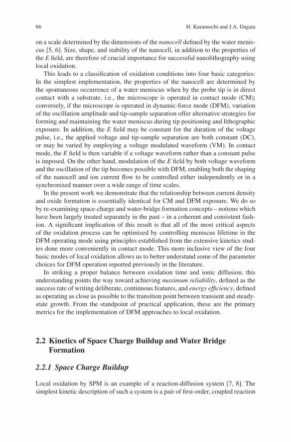
Garcia and co-workers [21, 22, 24] began investigating voltage-induced meniscusformation in 1998 by monitoring the oscillation amplitude during feedback ON/OFFconditions as DC pulse voltages were applied in noncontact mode. The transitionsof oscillation amplitude and tip-sample separation under successive switching ofthe voltage and feedback are illustrated in Fig. 2.1. Step I illustrates the cantileveroscillation amplitude (points) and tip-substrate separation (dashed line) for normalSPM operating conditions, i.e., voltage OFF, feedback ON. Step II demonstratesthe reduction in both parameters under the voltage ON, feedback OFF state. Thiswas interpreted as representing the impact on the cantilever oscillation due to theaddition of the electrostatic force between the tip and substrate. Step III indicatesthat a reduced amplitude condition persists in the voltage OFF, feedback OFF state,although the tip-sample separation increases to an intermediate position between theStep I and Step II positions. This indicates that a water meniscus clearly forms in the
Fig. 2.1 Observation ofelectrostatic force and waterbridge formation duringdynamic force oxidation:Cantilever oscillationamplitude as a function oftime before, during, and afterthe formation of an oxide dot.[Source: R. Garcia et al. [21],figure 1. Copyright ©American Institute ofPhysics]
2 Local Oxidation Using Dynamic Force Mode: Toward Higher Reliability. . . 69
course of Step II, as the original authors conclude. The final step returns the systemto the Step I state, increasing the larger oscillation amplitude corresponding to itsfeedback ON set point value, rupturing the meniscus and returning the tip-substrateseparation to its pre-determined value.
The work by Calleja et al. [24] also investigated the threshold voltage requiredfor the formation of the water bridge. The voltage pulse required to form a waterbridge was found to be greater than that for the subsequent oxidation reaction fora given tip-substrate separation. The capacitance between water layers on surfacesof the energized tip and substrate is strongly non-uniform due to the curvature ofthe tip and this induces a surface tension gradient of these water films. More recentwork has included computational efforts under continuum assumptions, i.e., withoutconsideration of ionic concentration and its reorganization and mobility within thesefilms. We examine this question in the following section since it is a critical elementfor understanding local oxidation in the short-pulse/fast-scan speed limit.
2.2.3 Combining the Two Concepts
Although many details of space charge buildup and water bridge formation havebeen established independently in recent years, there has not been a concerted effortto unify the basic principles articulated above into a coherent understanding of thenanocell, especially under dynamic conditions. This makes it particularly difficult toevaluate various approaches to DFM oxidation and reach a consensus on an entirelyoptimized methodology for local oxidation. This chapter certainly doesn’t providea final answer. However, in a pair of articles published in 2004 [26, 27] we dis-cussed experiments examining current, capacitance, and charge under contact andnoncontact conditions. Here we mention a few conclusions from that work whichprovides guidance for interpreting already published results, Section 2.3, as well asperforming new DFM oxidation experiments, Section 2.4, based on these efforts tointentionally link the space charge and meniscus formation concepts.
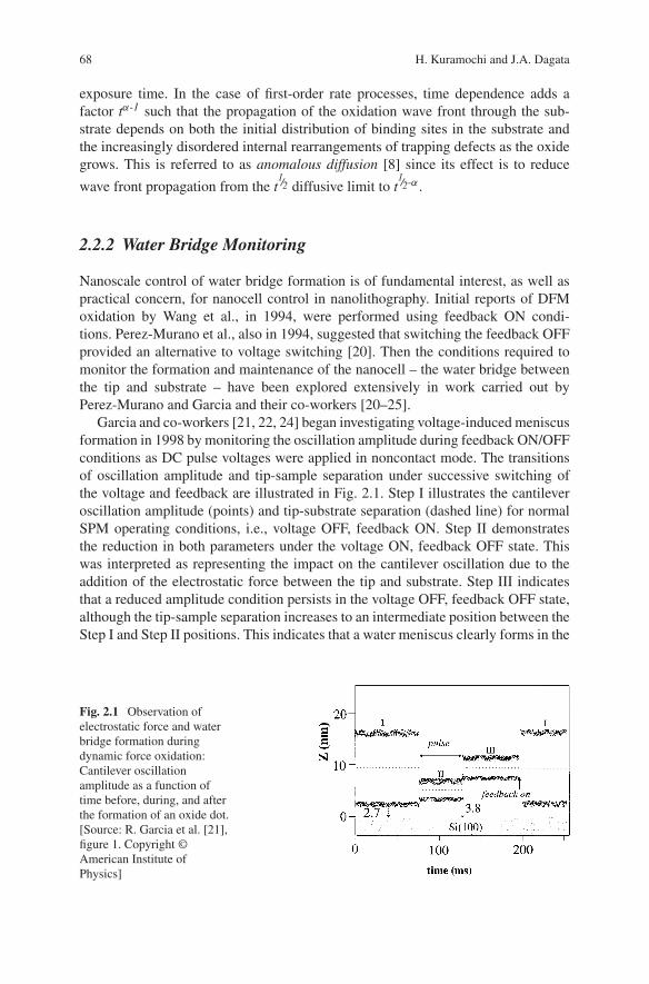
Now, the experiment in Fig. 2.1 [21], on its own, provides no information aboutcharge deposited and current flow that actually occurs as voltage is applied throughthe meniscus. Figure 2.2 presents results reported by us and our colleagues in 2003[28]. In this work we monitor simultaneously the cantilever deflection and currentmeasurements for a force-distance curve. Note that the voltage is 12 V, 40%RH,40 N/m. This simple measurement reveals that electrostatic bending of the cantileveroccurs until the force overcomes the resistance of the cantilever. At this point in theforce curve, a current of about 15 pA flows momentarily through the tip-samplejunction and drops off as oxidation takes place. The oxidation reaction persists untilthe mechanical pull-off force exceeds the attractive surface tension of the nanocell.Prior to pull-off, the attractive force associated with the nanocell reaches a point atwhich it is no longer in contact with the substrate. What is interesting here is that ifwe plot the current vs. the actual tip-surface separation (rather than z displacement);we see that current increases from 1 to 2 pA before the meniscus is ruptured. Thisapparently paradoxical current increase can be explained: By moving the tip out
70 H. Kuramochi and J.A. Dagata
(a)
(b)
(c)
Fig. 2.2 Observation ofsimultaneous electrostaticcantilever bending andcurrent flow during a forcecurve (voltage ON, feedbackOFF): (a) Cantileverdeflection and (b) current as afunction of z-displacement.(c) Current as a function oftip-surface separation as thetip retracts from the substrate.Tip-surface separation is thez-displacement plus cantileverdeflection. [Source: F.Perez-Murano et al. [28],figure 1. Copyright ©American Institute ofPhysics]
of direct contact with the surface, ionic charge can be reorganized, and therebyreduced, allowing current across the junction to increase.
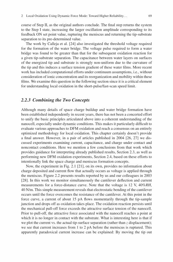
The measurement illustrated in Fig. 2.2 thus provides a complementary viewto the one established in Fig. 2.1 in the sense that the connection between currentflow and tip-substrate separation are correlated directly during the approach andretract cycles. Furthermore, the relationship between oxide volume and current canbe investigated in detail. Figure 2.3 [27] again demonstrates the necessity of thewater bridge but the experiment incorporates an important additional feature: Hereoxide growth for identical pulse conditions (13 and 18 V, 1 s) performed undercontact and noncontact conditions are compared. Note that the peak current obtainedwhen the tip is in repulsive contact is on the order 10 nA whereas it is on the orderof 1 nA if the current flows through a water meniscus. What is indeed interestingabout this measurement is that the height, diameter, and volume of the oxide featureproduced is nearly identical for the same exposure conditions regardless of whetheror not the tip is in direct contact with the substrate. We interpreted this measurementto mean that considerable excess, i.e., non-faradaic, current occurs if the tip is indirect contact with the substrate; in contrast, essentially only faradaic current occurs
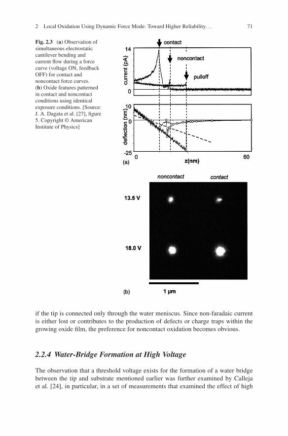
2 Local Oxidation Using Dynamic Force Mode: Toward Higher Reliability. . . 71
Fig. 2.3 (a) Observation ofsimultaneous electrostaticcantilever bending andcurrent flow during a forcecurve (voltage ON, feedbackOFF) for contact andnoncontact force curves.(b) Oxide features patternedin contact and noncontactconditions using identicalexposure conditions. [Source:J. A. Dagata et al. [27], figure5. Copyright © AmericanInstitute of Physics]
if the tip is connected only through the water meniscus. Since non-faradaic currentis either lost or contributes to the production of defects or charge traps within thegrowing oxide film, the preference for noncontact oxidation becomes obvious.
2.2.4 Water-Bridge Formation at High Voltage
The observation that a threshold voltage exists for the formation of a water bridgebetween the tip and substrate mentioned earlier was further examined by Callejaet al. [24], in particular, in a set of measurements that examined the effect of high

72 H. Kuramochi and J.A. Dagata
0
8
heig
ht (
nm)
10−4 10−3 10−2 10−1 100 101
10−4 10−3 10−2 10−1 100 101
10−4 10−3 10−2 10−1 100 1010
0.07
time (s)
aspe
ct r
atio
0
300
wid
th (
nm)
Fig. 2.4 Semi-log plots ofoxide height, width, andaspect ratio (height: width) ofdots formed during feedbackOFF DFM oxidation as afunction of exposure time.Curves increase in regularvoltage increments from low(8 V) to high (24 V) in eachpanel. Experimental data(circles) from Reference 24,figure 2]. Calculated values(continuous lines) are basedon previously publishedAlberty & Miller rateconstants for siliconpublished in Reference 10
voltage and short exposure time on oxide growth rate for feedback OFF DFM mode.Their conclusion was that high-voltage, short-time pulses provide an advantagewhen patterning in this mode. In Fig. 2.4, we replot their data – presented as height(h), width (w), and time (t) in Figs. 2.1 and 2.2 of their article – as aspect ratio (h/w)vs. t. These experimental feedback OFF DFM oxidation data are compared to cal-culated values obtained from the Alberty & Miller kinetic model and rate constantparameters reported in Reference 10. What is interesting is that the applied voltagein this experiment ranged from 8 to 24 V, much higher than the range of voltageusually studied. Our manner of plotting the data reveals the appearance of a distinctmaximum in the aspect ratio, at increasingly shorter times, as the applied voltageis increased. Figure 2.4 confirms their conclusion, but offers additional insight intoa unique aspect of DFM lithography: The possibility of extremely fast oxidation,albeit if one is willing to accept limited oxide thickness of about 3 nm or so.
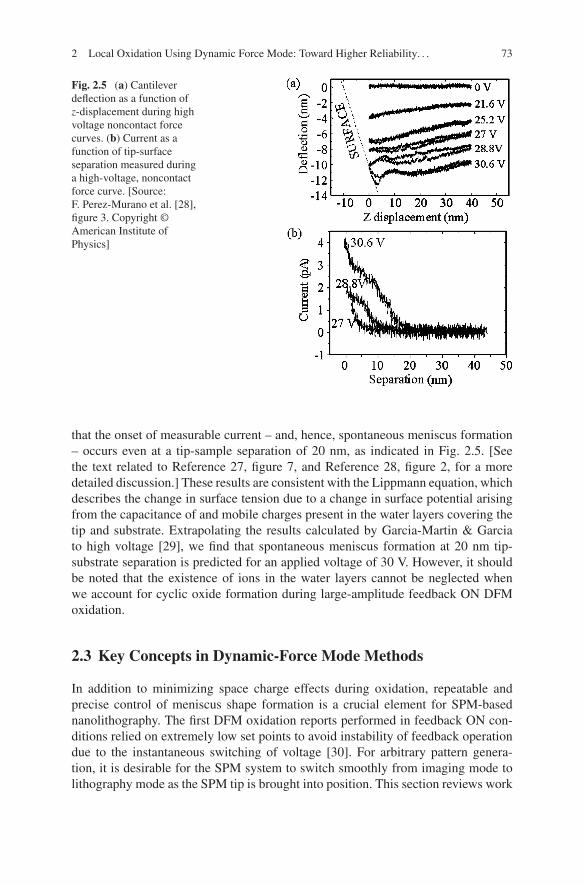
The benefits of high-voltage oxidation in DFM do not end with short pulse times.Simultaneous cantilever deflection and current measurements obtained during aforce–distance curve using applied voltages in the range of 20 V to 30 V reveal
2 Local Oxidation Using Dynamic Force Mode: Toward Higher Reliability. . . 73
Fig. 2.5 (a) Cantileverdeflection as a function ofz-displacement during highvoltage noncontact forcecurves. (b) Current as afunction of tip-surfaceseparation measured duringa high-voltage, noncontactforce curve. [Source:F. Perez-Murano et al. [28],figure 3. Copyright ©American Institute ofPhysics]
that the onset of measurable current – and, hence, spontaneous meniscus formation– occurs even at a tip-sample separation of 20 nm, as indicated in Fig. 2.5. [Seethe text related to Reference 27, figure 7, and Reference 28, figure 2, for a moredetailed discussion.] These results are consistent with the Lippmann equation, whichdescribes the change in surface tension due to a change in surface potential arisingfrom the capacitance of and mobile charges present in the water layers covering thetip and substrate. Extrapolating the results calculated by Garcia-Martin & Garciato high voltage [29], we find that spontaneous meniscus formation at 20 nm tip-substrate separation is predicted for an applied voltage of 30 V. However, it shouldbe noted that the existence of ions in the water layers cannot be neglected whenwe account for cyclic oxide formation during large-amplitude feedback ON DFMoxidation.
2.3 Key Concepts in Dynamic-Force Mode Methods
In addition to minimizing space charge effects during oxidation, repeatable andprecise control of meniscus shape formation is a crucial element for SPM-basednanolithography. The first DFM oxidation reports performed in feedback ON con-ditions relied on extremely low set points to avoid instability of feedback operationdue to the instantaneous switching of voltage [30]. For arbitrary pattern genera-tion, it is desirable for the SPM system to switch smoothly from imaging mode tolithography mode as the SPM tip is brought into position. This section reviews work

74 H. Kuramochi and J.A. Dagata
Table 2.1 Parameters reported in selected DFM oxidation approaches (feedback ON)
Maximumvoltage (V) RH(%) Substrate
Oxidationtime or scanspeed
Tip coating /springconstant(N/m)
Oscillationamplitude(nm)
Vicary and Miles[34]
12 60 p-Si:H 2 cm/s PtIr 42 5
Graf et al. [38] 16 42 n-GaAs 2 μm/s TiPt 40 –
Kuramochi et al.[39]
10 45 p-Si:H 1 μm/s Rh 20 258
Clement et al.[33]
30 70 n-Si:Hw/oxideregrowth
2 μm/s – 40 20
Legrand andStievenard[32]
12 – Si:H – – 12
Fontaine et al.[40]
12 Si:H 10 μm/s PtTi 40 2
reported in several articles selected from the feedback ON DFM oxidation literature.These articles are listed in the Table 2.1 and were chosen because they specificallyaddress control factors affecting DFM oxidation performance.
2.3.1 Synchronized Pulse, Part I
Voltage modulation (VM), i.e., using a series of unipolar or bipolar pulses, ratherthan a single continuous one, originated in our initial investigations of space chargebuildup during local oxidation. In 1998 we were interested in validating the inter-facial nature of the space charge as revealed by electrical force microscopy (EFM)measurements of oxide features produced under CM conditions as a function of thedoping type and level of silicon substrates [15, 16]. The frequency dependence ofthe enhancement and the oxide density variation as a function of dopant form anecessary logical connection to the classic literature of low-temperature oxidation[11, 12].
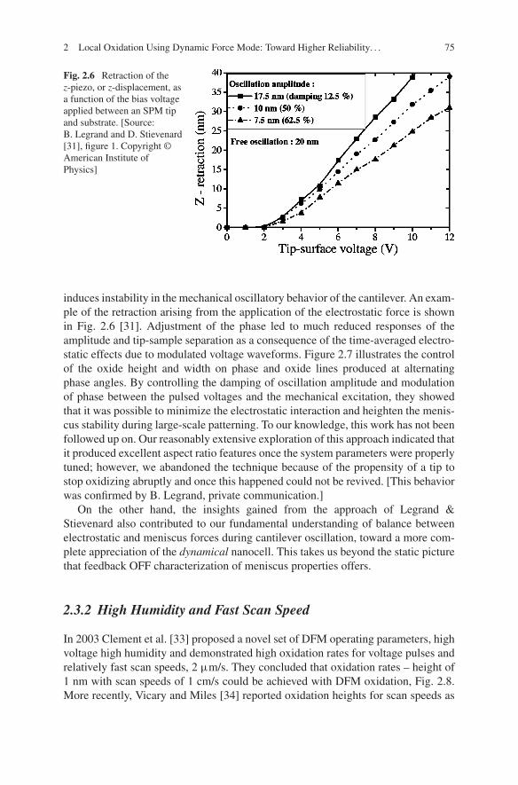
The implication that voltage modulation enhances oxidation by reducing thebuild up of space charge tested a certain hypothesis. In a more practical sense, itwas of interest for producing thicker oxide features and avoiding the slow-growth,steady-state regime and, especially, lateral diffusion that reduced the aspect ratio ofoxide features. VM techniques provide an important benefit specific to DFM oxi-dation, as first described by Legrand & Stievenard in 1999 [31, 32]. Their principalconcern was to overcome the old problem of avoiding the discontinuities producedby voltage switching during feedback ON operations. They studied the effect ofsynchronizing the voltage pulses to coincide with the phase of the cantilever oscilla-tion. The electrostatic force, if applied under instantaneous feedback-on conditions,
2 Local Oxidation Using Dynamic Force Mode: Toward Higher Reliability. . . 75
Fig. 2.6 Retraction of thez-piezo, or z-displacement, asa function of the bias voltageapplied between an SPM tipand substrate. [Source:B. Legrand and D. Stievenard[31], figure 1. Copyright ©American Institute ofPhysics]
induces instability in the mechanical oscillatory behavior of the cantilever. An exam-ple of the retraction arising from the application of the electrostatic force is shownin Fig. 2.6 [31]. Adjustment of the phase led to much reduced responses of theamplitude and tip-sample separation as a consequence of the time-averaged electro-static effects due to modulated voltage waveforms. Figure 2.7 illustrates the controlof the oxide height and width on phase and oxide lines produced at alternatingphase angles. By controlling the damping of oscillation amplitude and modulationof phase between the pulsed voltages and the mechanical excitation, they showedthat it was possible to minimize the electrostatic interaction and heighten the menis-cus stability during large-scale patterning. To our knowledge, this work has not beenfollowed up on. Our reasonably extensive exploration of this approach indicated thatit produced excellent aspect ratio features once the system parameters were properlytuned; however, we abandoned the technique because of the propensity of a tip tostop oxidizing abruptly and once this happened could not be revived. [This behaviorwas confirmed by B. Legrand, private communication.]
On the other hand, the insights gained from the approach of Legrand &Stievenard also contributed to our fundamental understanding of balance betweenelectrostatic and meniscus forces during cantilever oscillation, toward a more com-plete appreciation of the dynamical nanocell. This takes us beyond the static picturethat feedback OFF characterization of meniscus properties offers.
2.3.2 High Humidity and Fast Scan Speed
In 2003 Clement et al. [33] proposed a novel set of DFM operating parameters, highvoltage high humidity and demonstrated high oxidation rates for voltage pulses andrelatively fast scan speeds, 2 μm/s. They concluded that oxidation rates – height of1 nm with scan speeds of 1 cm/s could be achieved with DFM oxidation, Fig. 2.8.More recently, Vicary and Miles [34] reported oxidation heights for scan speeds as

76 H. Kuramochi and J.A. Dagata
(a)
(b)
Fig. 2.7 Synchronized pulse DFM oxidation. (a) Variation of the oxide height andwidth as a function of the phase angle between voltage pulse and cantilever oscillation.(b) Effect of phase modulation on oxide height and width. [Source: B. Legrand and D. Stievenard[32], figures 2 and 3. Copyright © American Institute of Physics]
high as 2 cm/s and single pulse oxidation for times as short as 500 ns, Fig. 2.9. Notethat the width or diameter of the oxide features is not an important considerationsince these experiments were performed well within the transient region. Parametersfor both are listed in the Table 2.1. Note the specific combination of (V, RH, A) –voltage, RH, and cantilever oscillation amplitude values used by Clement et al.(30 V, 70%RH, 20 nm) and Vicary & Miles (12 V, 60%RH, 5 nm) to obtain1–2 nm of oxide height. Both authors attribute the persistence of the water meniscusas the key explanation for the success of their respective techniques.

2 Local Oxidation Using Dynamic Force Mode: Toward Higher Reliability. . . 77
Fig. 2.8 SPM topographicimage (a) and line profile(b) of oxide dots producedusing high-voltage, highhumidity DFM oxidation.[Source: N. Clement et al.[33], figure 1. Copyright ©2010 American VacuumSociety]
Fig. 2.9 SPM topographic image of oxide dots produced using high probe speed DFM oxidation.Exposure time varies from 100 μs in panel (a) to 500 ns in panel (e). [Source: J. A. Vicary andM. J. Miles [34], figure 2. Copyright © 2010 Elsevier B.V.]
On the basis of our unified concept of the nanocell, we say that all probe-basedoxidation follows from the same fundamental process, i.e., that a single processoperates from the transient, fast-growth regime, at the transition point, and through-out the steady-state, slow-growth regime. After all, this is what the coupled kinetic

78 H. Kuramochi and J.A. Dagata
equations of Alberty & Miller are all about. If the fundamentals are shared, it mustmean that the (V, RH, A) parameter space allows a reduced RH if A is increased, forinstance. Similarly, higher V allows a larger A, and so forth.
These experimental results have been interpreted by the authors by framing theprincipal question in terms of a “limiting oxidation rate” and “mechanical pressure”.Both Clement et al. and Vicary & Miles chose to pick up the discussion beginningwith interpretations given in the work of Snow et al. [35–37] on CM oxidation andTello & Garcia and co-workers [25] concerning differences between CM and DFMoxidation.
For example, Clement et al. state [33] “Therefore the main difference with thepulsed voltage technique is the higher tip oscillation amplitude combined with highhumidity ratio to avoid mechanical pressure during oxide growth and to increasethe amount of oxidizing species. This also suggests that oxidizing species are thelimiting factor for AFM oxidation.”
The early conclusions of Snow are inconsistent with the space charge model andthe view of the nanocell presented earlier. Snow et al. [37] concluded that “. . .therate-limiting step of the oxidation process is the production of O anions from theambient humidity.” This conclusion was based on a clearly erroneous interpretationof data presented in Fig. 2.1 of their paper. As we have shown in Reference 28,figure 6, lateral spreading at high humidity leads to increased oxide feature width –and at the near saturation levels, 95%RH, used in the Snow work – accounts quan-titatively for their observations, not condensation from the vapor. Keep in mind thattheir vapour-to-liquid transition hypothesis was never actually tested. In Reference29, figure 7 we demonstrate that ionic mobility within the water layers, not conden-sation from the vapour, explains their results. Current flow through the nanocell isnecessary for oxidation, as demonstrated directly in Figs. 2.3 and 2.4. Furthermore,the long-range formation of a water bridge in Fig. 2.5 agrees qualitatively and quan-titatively with the capacitance calculations of Garcia-Martin & Garcia [31]. Quitesimply, water layers are always present on the tip and substrate surfaces above20%RH and, if they are not, oxidation does not occur.
Vicary & Miles [34] engage in an equally doubtful line of reasoning in attempt-ing to explain results shown in Fig. 2.2 of their paper: In order to account for theobservation that oxide growth ceases entirely for pulse durations longer than 20 μs,they invoke a model proposed by Tello & Garcia [25] in which the growth rate dur-ing CM oxidation is suppressed because of the additional work done by the growingoxide feature to bend the cantilever. [Note, again, that this hypothesis has never beentested experimentally.] The idea applied to the DFM case is that, due to the shortduration of the cantilever oscillation and oxidation pulse in their experiments, thefeedback loop does not raise the tip in response to the growth of oxide. The difficultywith this reasoning is that it ignores the degrees of freedom that oxyanions possessin the nanocell – and here we specifically include lateral diffusion within both thewater meniscus and the oxide. In the nanocell, anions are not constrained by a fixedboundary, rather, they respond by diffusing laterally, a dissipative mechanism at theheart of the space-charge concept.

2 Local Oxidation Using Dynamic Force Mode: Toward Higher Reliability. . . 79
2.3.3 Synchronized Pulse, Part II
Graf et al. [38] tried optimizing the ratio of oxidation time to total pulse cycle in theirapproach to voltage modulation during feedback ON DFM oxidation of Ga[Al]Asand n-Si. To achieve the most stable and efficient lithographic conditions, theseauthors suggested that it is necessary to determine an effective oxidation time ratiofor the system. They found that the feedback ON DFM requirement of operatingwith a low set point, i.e., 8% < DC set < 16% of the free oscillation amplitude, asothers had reported, could be substantially increased to a range of 10% < VM set< 40%, because the time averaged electrostatic force experienced by the feedbackloop is reduced, similar to the reasoning of Legrand & Stievenard [31], however,without the additional step of exactly synchronizing the voltage pulse and cantileveroscillation.
Another interesting result that they report is one bearing directly on the questionof comparative reliability of VM versus DC exposure for feedback ON DFM oxi-dation. The series of lines shown in the SPM image of Fig. 2.10 are representative
Fig. 2.10 Comparative reliability of DC and voltage modulation, referred to as VM in the textand labeled AC in the figure. SPM topographic image presents alternating series of oxide linesproduced by DFM oxidation on undoped GaAs. [Source: D. Graf et al. [38], figure 5. Copyright ©American Institute of Physics]
80 H. Kuramochi and J.A. Dagata
of a much larger set of exposures. As Graf et al. [38] note “In ac oxidation we havethe chance to pick up the water film in each cycle. . .in the dc mode, however, onceit failed at the beginning, the strong additional electrostatic damping will keep thetip too far from the sample surface for a water bridge to form.” By operating in apulsed mode situation, even an inevitable disruption of the nanocell can be repairedon the following voltage cycle. We gradually become aware of the possibility thata persistent meniscus is not actually necessary for reliable DFM oxidation. In otherwords, it may be essential for a stable feedback loop, but not for lithography. As wedemonstrate shortly, the persistence of the meniscus is not even needed for that.
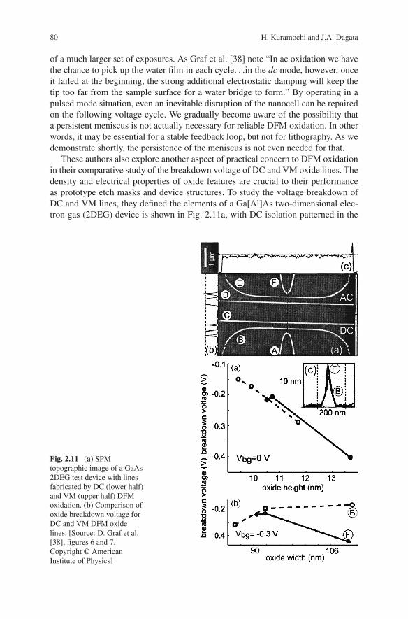
These authors also explore another aspect of practical concern to DFM oxidationin their comparative study of the breakdown voltage of DC and VM oxide lines. Thedensity and electrical properties of oxide features are crucial to their performanceas prototype etch masks and device structures. To study the voltage breakdown ofDC and VM lines, they defined the elements of a Ga[Al]As two-dimensional elec-tron gas (2DEG) device is shown in Fig. 2.11a, with DC isolation patterned in the
Fig. 2.11 (a) SPMtopographic image of a GaAs2DEG test device with linesfabricated by DC (lower half)and VM (upper half) DFMoxidation. (b) Comparison ofoxide breakdown voltage forDC and VM DFM oxidelines. [Source: D. Graf et al.[38], figures 6 and 7.Copyright © AmericanInstitute of Physics]
2 Local Oxidation Using Dynamic Force Mode: Toward Higher Reliability. . . 81
lower half and VM isolation patterned in the upper half of the overall structure. Abreakdown threshold corresponding to 10 pA was determined for each oxide line inthe series and plotted in Fig. 2.11b. They attribute the substantial increase of 186%in breakdown voltage to the more uniformly continuous nature of the VM-patternedoxide. While the authors conclude that the final confinement potential of each regionof the test device is comparable for DC and VM methods – in doing so they attachmore significance to the magnetoresitive results than to oxide quality directly – itis useful to generalize from the special case of remote 2DEG patterning to otherdevice applications.
Voltage breakdown and oxide homogeneity may be far more important metricsfor silicon-oxide tunnel barriers or anisotropic etch resistance, for example. It isworthwhile to mention that some years ago we also examined the density variationfor local silicon-oxide device structures patterned by DC and VM techniques [18].Furthermore, annealing effects on the oxide density and interfacial defect densityof the oxide features were pointed out and the reduction of such defects producedduring the patterning of device structures by local oxidation is necessary in order toachieve acceptable device performance in these systems.
2.4 New Aspects of Reaction Control by Probe Speed
This section sheds new light on achieving the highest possible reliability, writingspeed, and large-scale precision through simultaneous analysis of oxide-volumeand current-flow measurements during DFM oxidation. We have already reviewedthe formation of the nanocell on the basis of investigations in the feedback OFFcondition in the foregoing section. While certainly adequate for gaining deeperunderstanding of the underlying kinetic process, operating in this mode limits pat-terning to single point-like features which is unsuitable for the practical applicationsof interest here.
It is for this reason that we focus our attention on feedback ON DFM in the restof this chapter. Furthermore, we evaluate CM and feedback ON DFM oxidation asan explicit function of probe speed, v, during fabrication of continuous oxide linesand area features [39–45]. Since probe speed is more complicated than a simpleinversion of time in the case of VM feedback ON DFM oxidation, when “time” isdiscussed in the following, a careful distinction between voltage-pulse duration andmeniscus-formation cycles [39] must be made. Such a distinction does not arise forCM oxidation of course.
2.4.1 Small and Large Amplitude
Most of the authors of articles listed in the Table 2.1, Legrand & Stievenard,Fontaine et al., Vicary & Miles, and Graf et al., have emphasized how the stabilityof the cantilever oscillation depends on selecting a small value of the oscillationamplitude and a low amplitude set point during feedback ON DFM oxidation. Bycontrast, we and our colleagues have shown that there is another way to look at the
82 H. Kuramochi and J.A. Dagata
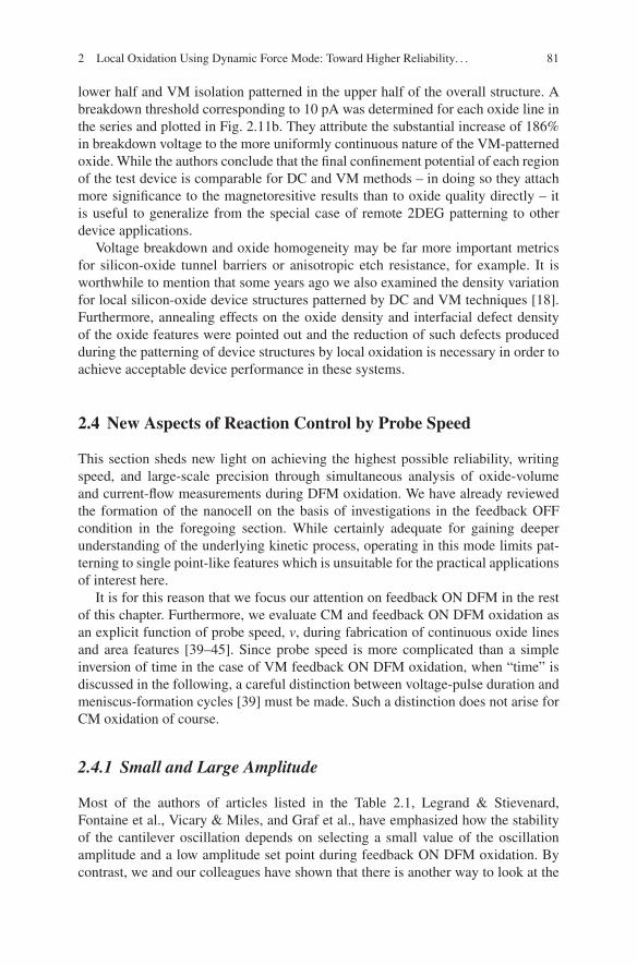
DFM control problem – by using DC voltage but working at a very large amplitude.Cyclic meniscus formation was also found to occur when oxidation was performedwith the cantilever driven at high oscillation amplitudes and constant DC voltagewas applied. This is comparable to performing oxidation using pulsed voltages. Wefound that during that part of the cycle when the tip-sample separation is small-est, the meniscus length is essentially constant for fixed voltage and RH from cycleto cycle. Thus a meniscus could be formed periodically at large amplitude settings(>200 nm). In this case, since maintaining feedback in its active state is possibleunder these conditions, we can avoid electrostatic damping, and that as the probetip makes its closest approach to the substrate, a water meniscus is regenerated asit would be in the case of a voltage pulse. Meniscus lifetime could be controlled tosub-microsecond order by adjusting the cantilever amplitude setting or by modulat-ing its oscillation amplitude by altering the probe-sample distance as illustrated inFig. 2.12 [23]. This regeneration is both spontaneous and more reliable as revealedin the foregoing sections.
Fig. 2.12 Large-amplitude dynamic force mode oxidation. (a) Decrease of the cantilever oscilla-tion amplitude, Δz = Δd − Δs, calculated from the z-piezo displacement, Δd, and the slope ofthe substrate, Δs. When used in the feedback OFF condition, the minimum oscillation amplitudenecessary for stable meniscus rupture may be obtained. [Source: H. Kuramochi et al. [39], figure 1.Copyright © American Institute of Physics]
2 Local Oxidation Using Dynamic Force Mode: Toward Higher Reliability. . . 83
2.4.2 Comparison of Contact and Dynamic Force Mode Oxidation
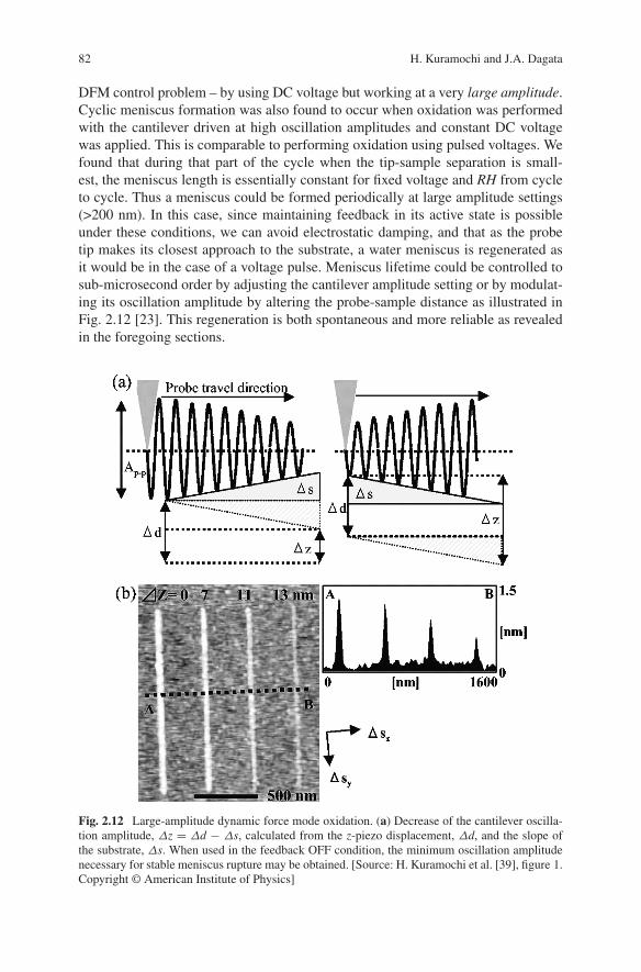
Efforts to employ feedback ON DFM oxidation have proceeded in parallel withfeedback OFF investigations. Figure 2.13 reproduces early results from Fontaineet al. comparing oxide growth rate for CM and feedback ON DFM oxidation asa function of probe speed [40]. The general trends are that the oxide height, orthickness, and the maximum probe speed that can be used for DFM are somewhatless than for CM, although the voltage-dependent slopes are similar. Note also thatthe oscillation of the cantilever is set to a remarkably low value of 2 nm in theseexperiments.
What we now wish to examine is how current and volume calculated forCM and DFM vary in such measurements. Moreover, we want to determine ifrupturing and reforming the nanocell during each oscillation cycle of the probetip – large-amplitude DFM lithography – produces a qualitatively similar oxideas low-amplitude DFM lithography. For this purpose, comparative CM and DFMexperiments were carried out. Lithographic patterning was performed using anenvironmental control SPM unit at a constant relative humidity of 50% at roomtemperature. Probe speed was varied over a range of 0.1–20 μm/s. A hydrogen pas-sivated p-type Si(001) sample (1 − 10 � · cm) was used as the sample. Rh-coatedSi cantilevers for CM (∼0.1 N/m), for DFM (∼20 N/m) and modified cantilevers
(b)
(a)
Fig. 2.13 Comparison ofcontact mode and dynamicforce mode oxidation as afunction of probe speed:(a) Oxide line height by CM.(b) Oxide line height byDFM. [Source: P. A. Fontaineet al. [40], figures 10 and 17.Copyright © AmericanInstitute of Physics]
84 H. Kuramochi and J.A. Dagata
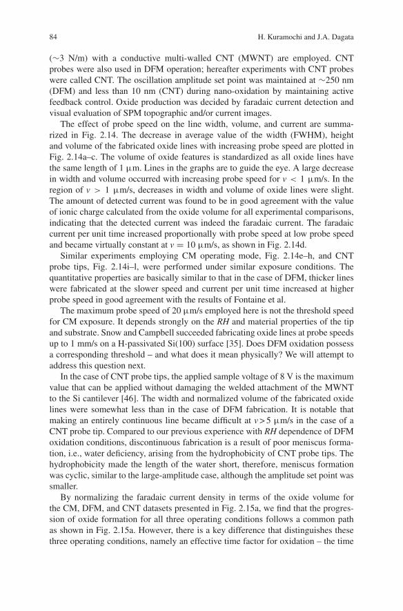
(∼3 N/m) with a conductive multi-walled CNT (MWNT) are employed. CNTprobes were also used in DFM operation; hereafter experiments with CNT probeswere called CNT. The oscillation amplitude set point was maintained at ∼250 nm(DFM) and less than 10 nm (CNT) during nano-oxidation by maintaining activefeedback control. Oxide production was decided by faradaic current detection andvisual evaluation of SPM topographic and/or current images.
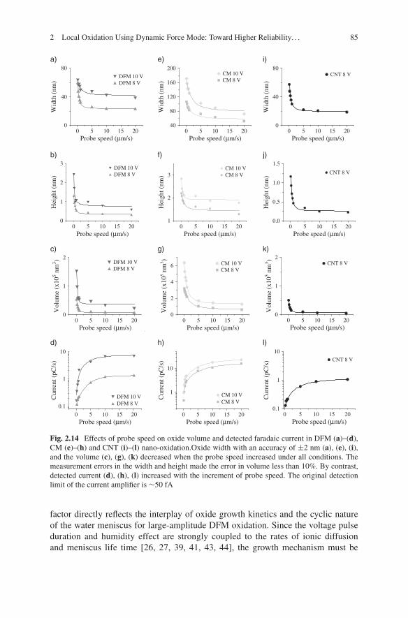
The effect of probe speed on the line width, volume, and current are summa-rized in Fig. 2.14. The decrease in average value of the width (FWHM), heightand volume of the fabricated oxide lines with increasing probe speed are plotted inFig. 2.14a–c. The volume of oxide features is standardized as all oxide lines havethe same length of 1 μm. Lines in the graphs are to guide the eye. A large decreasein width and volume occurred with increasing probe speed for v < 1 μm/s. In theregion of v > 1 μm/s, decreases in width and volume of oxide lines were slight.The amount of detected current was found to be in good agreement with the valueof ionic charge calculated from the oxide volume for all experimental comparisons,indicating that the detected current was indeed the faradaic current. The faradaiccurrent per unit time increased proportionally with probe speed at low probe speedand became virtually constant at v = 10 μm/s, as shown in Fig. 2.14d.
Similar experiments employing CM operating mode, Fig. 2.14e–h, and CNTprobe tips, Fig. 2.14i–l, were performed under similar exposure conditions. Thequantitative properties are basically similar to that in the case of DFM, thicker lineswere fabricated at the slower speed and current per unit time increased at higherprobe speed in good agreement with the results of Fontaine et al.
The maximum probe speed of 20 μm/s employed here is not the threshold speedfor CM exposure. It depends strongly on the RH and material properties of the tipand substrate. Snow and Campbell succeeded fabricating oxide lines at probe speedsup to 1 mm/s on a H-passivated Si(100) surface [35]. Does DFM oxidation possessa corresponding threshold – and what does it mean physically? We will attempt toaddress this question next.
In the case of CNT probe tips, the applied sample voltage of 8 V is the maximumvalue that can be applied without damaging the welded attachment of the MWNTto the Si cantilever [46]. The width and normalized volume of the fabricated oxidelines were somewhat less than in the case of DFM fabrication. It is notable thatmaking an entirely continuous line became difficult at v > 5 μm/s in the case of aCNT probe tip. Compared to our previous experience with RH dependence of DFMoxidation conditions, discontinuous fabrication is a result of poor meniscus forma-tion, i.e., water deficiency, arising from the hydrophobicity of CNT probe tips. Thehydrophobicity made the length of the water short, therefore, meniscus formationwas cyclic, similar to the large-amplitude case, although the amplitude set point wassmaller.
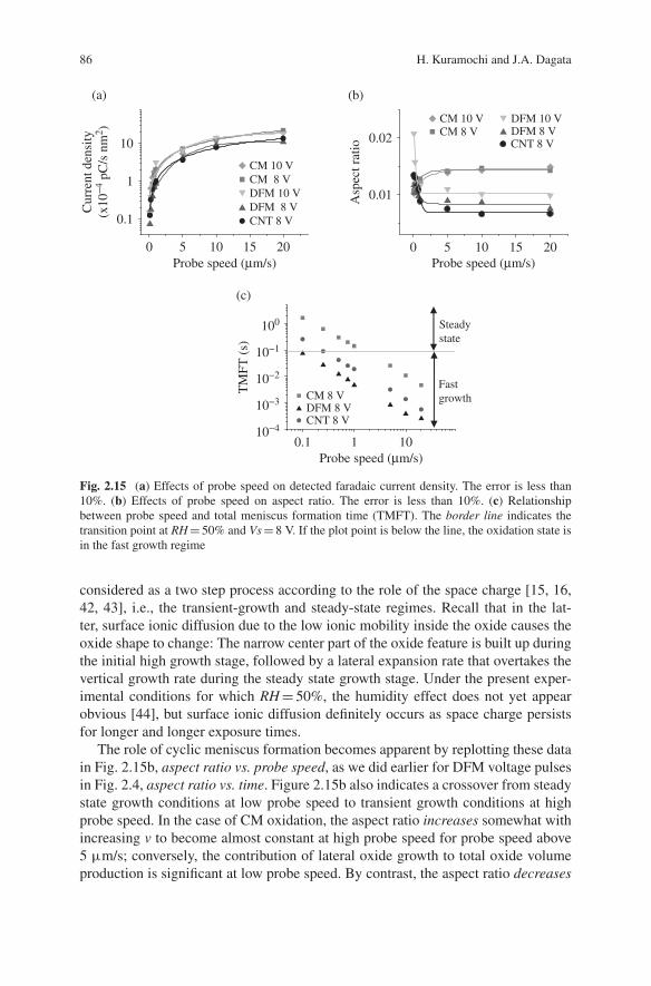
By normalizing the faradaic current density in terms of the oxide volume forthe CM, DFM, and CNT datasets presented in Fig. 2.15a, we find that the progres-sion of oxide formation for all three operating conditions follows a common pathas shown in Fig. 2.15a. However, there is a key difference that distinguishes thesethree operating conditions, namely an effective time factor for oxidation – the time
2 Local Oxidation Using Dynamic Force Mode: Toward Higher Reliability. . . 85
a)
0 5 10 15 200
40
80
DFM 10 VDFM 8 V
Wid
th (
nm)
Probe speed (μm/s)0 5 10 15 20
40
80
120
160
200CM 10 VCM 8 V
Wid
th (
nm)
Probe speed (μm/s)
e)
c)
0 5 10 15 20Probe speed (μm/s)
0
1
2
Vol
ume
(x10
5 nm
3 ) DFM 10 VDFM 8 V
g)
0 5 10 15 20Probe speed (μm/s)
Vol
ume
(x10
5 nm
3 )
0
2
4
6 CM 10 VCM 8 V
0
40
80
Wid
th (
nm)
0 5 10 15 20Probe speed (μm/s)
CNT 8 V
i)
0 5 10 15 20Probe speed (μm/s)
CNT 8 V
0.1
1
10
Cur
rent
(pC
/s)
l)
b)
0 5 10 15 20Probe speed (μm/s)
0
1
2
3
Hei
ght (
nm)
DFM 10 VDFM 8 V
d)
0 5 10 15 20Probe speed (μm/s)
0.1
1
10
Cur
rent
(pC
/s)
DFM 10 VDFM 8 V
h)
0 5 10 15 20Probe speed (μm/s)
1
10
Cur
rent
(pC
/s)
CM 10 VCM 8 V
f)
0 5 10 15 20Probe speed (μm/s)
1
2
3
Hei
ght (
nm)
CM 10 VCM 8 V
k)
0 5 10 15 20Probe speed (μm/s)
Vol
ume
(x10
5 nm
3 )CNT 8 V
0
1
2
j)
0 5 10 15 20Probe speed (μm/s)
0.0
0.5
1.0
1.5
CNT 8 V
Hei
ght (
nm)
Fig. 2.14 Effects of probe speed on oxide volume and detected faradaic current in DFM (a)–(d),CM (e)–(h) and CNT (i)–(l) nano-oxidation.Oxide width with an accuracy of ±2 nm (a), (e), (i),and the volume (c), (g), (k) decreased when the probe speed increased under all conditions. Themeasurement errors in the width and height made the error in volume less than 10%. By contrast,detected current (d), (h), (l) increased with the increment of probe speed. The original detectionlimit of the current amplifier is ∼50 fA
factor directly reflects the interplay of oxide growth kinetics and the cyclic natureof the water meniscus for large-amplitude DFM oxidation. Since the voltage pulseduration and humidity effect are strongly coupled to the rates of ionic diffusionand meniscus life time [26, 27, 39, 41, 43, 44], the growth mechanism must be
86 H. Kuramochi and J.A. Dagata
0 5 10 15 20Probe speed (μm/s)
0.01
0.02
Asp
ect r
atio
CM 10 V CM 8 V
DFM 10 VDFM 8 VCNT 8 V
(b)
0 5 10 15 20
0.1
1
10
Cur
rent
den
sity
(x10
−4 p
C/s
nm
2 )
Probe speed (μm/s)
CM 10 VCM 8 VDFM 10 VDFM 8 VCNT 8 V
(a)
Probe speed (μm/s)0.1 1 10
10−4
10−3
10−2
10−1
100
CM 8 VDFM 8 VCNT 8 V
TM
FT (
s)
Steadystate
Fastgrowth
(c)
Fig. 2.15 (a) Effects of probe speed on detected faradaic current density. The error is less than10%. (b) Effects of probe speed on aspect ratio. The error is less than 10%. (c) Relationshipbetween probe speed and total meniscus formation time (TMFT). The border line indicates thetransition point at RH = 50% and Vs = 8 V. If the plot point is below the line, the oxidation state isin the fast growth regime
considered as a two step process according to the role of the space charge [15, 16,42, 43], i.e., the transient-growth and steady-state regimes. Recall that in the lat-ter, surface ionic diffusion due to the low ionic mobility inside the oxide causes theoxide shape to change: The narrow center part of the oxide feature is built up duringthe initial high growth stage, followed by a lateral expansion rate that overtakes thevertical growth rate during the steady state growth stage. Under the present exper-imental conditions for which RH = 50%, the humidity effect does not yet appearobvious [44], but surface ionic diffusion definitely occurs as space charge persistsfor longer and longer exposure times.
The role of cyclic meniscus formation becomes apparent by replotting these datain Fig. 2.15b, aspect ratio vs. probe speed, as we did earlier for DFM voltage pulsesin Fig. 2.4, aspect ratio vs. time. Figure 2.15b also indicates a crossover from steadystate growth conditions at low probe speed to transient growth conditions at highprobe speed. In the case of CM oxidation, the aspect ratio increases somewhat withincreasing v to become almost constant at high probe speed for probe speed above5 μm/s; conversely, the contribution of lateral oxide growth to total oxide volumeproduction is significant at low probe speed. By contrast, the aspect ratio decreases
2 Local Oxidation Using Dynamic Force Mode: Toward Higher Reliability. . . 87
with the increase in probe speed in the case of DFM and CNT oxidation because ver-tical oxide growth continues during repeated oxidation of the same surface area –the system remains in the transient regime. The explanation is that meniscus forma-tion is cyclical, the effective oxidation time is very short in DFM, and the oxidationreaction terminates for a portion of every oscillation cycle before lateral ionic diffu-sion occurs [43]. Moreover, as the probe tip is displaced in response to the voltagepulse, water flows onto the fabricated oxide, which is considerably more hydrophilicthan the surrounding H-passivated Si surface. Water condensation is thus confinedto a narrow region of the meniscus directly beneath the probe tip and oxidation atthe base of the meniscus is suppressed.
2.4.3 Concept of the Total Meniscus Formation Time
As noted earlier, the first detailed investigations of DFM oxidation were performedunder greatly reduced oscillation amplitude of the cantilever. Careful monitoringof the amplitude is necessary to ensure stable meniscus formation during voltageswitching. Both the work of Garcia et al., Fig. 2.1, and Fontaine et al., Fig. 2.13,employed small oscillation amplitude, i.e., under feedback OFF and feedback ONDFM oxidation, respectively. The results shown in Figs. 2.12, 2.14 and 2.15 indicatethat operating with such small oscillation amplitudes is not necessary.
However, operating successfully in the large-amplitude regime requires a sepa-rate analysis of cyclic meniscus formation since the physical situation is qualita-tively different from the small-amplitude case. In this sense, feedback OFF DFMoxidation is more akin to CM exposure since the meniscus remains intact for theentire length of the voltage pulse. Thus we can define a total meniscus formationtime (TMFT) at a given location on the substrate to be d ms. (Consider that if theprobe speed is set at 1 μm/s, a meniscus of diameter d nm exposes a certain mini-mum area at a single location on the substrate for a duration of d ms.) But the TMFTfor large-amplitude DFM exposure depends also on the oscillation frequency of thecantilever and the amplitude set point – the cyclical existence of a meniscus andtherefore the propensity for oxidation through the nanocell and so may be quitedifferent [17, 18].
To make an estimate of such difference, we may assume that the oscillation of thecantilever is harmonic. For example, using resonant frequencies of 110 and 150 kHz,setting amplitudes of 250 and 5 nm, and a meniscus length of 8 and 2 nm for DFMand CNT cases [41, 46], respectively, then the meniscus formation time may beestimated to be about 0.83 and 1.97 μs, respectively. TMFTs calculated for theseexposure conditions follow a power-law relationship as shown in Fig. 2.15c. Nowif oxidation exposure occurs continuously at a given substrate location, the growthrate decreases due to the buildup of space charge. The transition point is about 0.09 sfor typical values of RH = 50% Vs = 8 V for CM oxidation [42].
On the other hand, if the TMFT is less than the transition point, the reactionstate remains in the fast growth regime as confirmed by the single-exponential fitto the data in Fig. 2.15c, exposure conditions for DFM mode correspond to the fast
88 H. Kuramochi and J.A. Dagata
growth regime. In the CNT case, v = 0.25 μm/s is just on the boundary between fastand slow growth conditions. If we want to operate CM oxidation in the fast growthregime, the probe speed must be set to 5 μm/s or higher. This trend is similar tothat of the humidity effect in CM, DFM and CNT cases [43]. Operation in the fastgrowth regime improves reproducibility in the size and shape of oxide features sincevariability due to ionic diffusion is reduced. Now it is clear that we can control thereaction state by the probe speed.
2.5 Conclusion: Toward Higher Reliability and Efficiency
From a practical standpoint, quality of the oxide feature and performance of theprocess have primary importance. Not only the final accuracy of the fabrication,i.e., pattern placement and aspect ratio, but also the reproducibility, stability, andenergy efficiency of the underlying process must be continuously refined. The roleof the most obvious control factors – (V, RH, t) – have become standard parametersreported by all authors in the field. Through this reporting we gain a sense of the“typical” range of the values employed in the published literature and thus are in abetter position to assess potential benefits of applying unusually large voltages orvery high RH. Then, on the other hand, there are examples that point to an effectivecombination both large V and RH, as shown in the work of Fontaine et al. [40].However, not all of these factors can at once be established in every experimentalsituation, leading to confusion over an optimized choice of parameters to employin practical processing conditions. And this is why we need to develop an adequateunderstanding of the full range of possibilities available with DFM oxidation. Thenthe question rests on how to incorporate the insight from demonstrations of fastscan/small amplitude by Vicary & Miles for instance with our novel approach whichshows that it is not essential for cantilever stability if the meniscus doesn’t reallyremain intact.
Our own view emphasizes that monitoring faradaic current and understanding theexistence of charged ions in the water layers, prior to and during the spontaneousformation of the water bridge are essential facts that account for the large-amplitudeoxidation results during feedback ON DFM. As we have shown, this ultimatelyreduces uncertainty in feature size and increases reliability for large-scale pattern-ing of fine features. It should be noted that measuring faradaic current in the caseof high conductivity samples may not always be possible. In this case, relying oneffective exposure “time” estimates calculated from the TMFT, although not exact,nevertheless provides a guide to suppressing lateral ionic diffusion and achievinghigher aspect ratio and enhanced reproducibility. An important feature of TMFT isthat it can be controlled externally by setting the dynamic operating parameters ofthe SPM instrument, namely, the resonance frequency, amplitude of the cantilever,RH, probe-sample distance and probe speed.
Energy efficiency is another important practical aspect of exposure control. Thehighest energy efficiency is achieved when the oxidation rate is maintained justbelow point at which the transition to lateral ionic diffusion becomes significant
2 Local Oxidation Using Dynamic Force Mode: Toward Higher Reliability. . . 89
and oxidation remains in the fast growth regime as long as possible. Direct faradaiccurrent detection during CM oxidation at a fixed point under actual process condi-tion is the best way to determine this transition point. It is also possible to estimateit by a calculation of the growth rate from the oxide volume production. The DFMoscillation and probe speed can then be adjusted so that TMFT occurs just beforethe transition point. This is possible because very rapid, cyclic meniscus formationin high-amplitude DFM operation mode is more precisely controllable than voltagepulses defined solely in terms of time.
This chapter has attempted to bring together the more familiar aspects of theelectrochemical nanocell with a critical discussion of feedback ON DFM oxida-tion. Future progress of local oxidation demands that novel refinements of thesemethods be investigated and the full implication for faster, more reliable operationuncovered and reported. Finally, let us express our hopes that such gains in process-ing efficiency will eventually find their way into truly high-throughput extensionsof local oxidation, e.g., high-voltage nanoimprint lithography [46, 47] or parallelcantilevers [48].
References
1. J. A. Dagata, J. Schneir, H. H. Harary, C. J. Evans, M. T. Postek and J. Bennett, Appl. Phys.Lett. 56, 2001 (1990).
2. A. A. Tseng, A. Notargiacomo and T. P. Chen, JVST B 23, 877 (2005).3. D. Stievenard and B. Legrand, Prog. Surf. Sci. 81, 112 (2006).4. J. A. Dagata, in Scanning Probe Microscopy: Electrical and electromechanical phenomena at
the nanoscale, edited S. Kalinin and A. Gruverman, Springer Press, New York (2007), Vol. II,p. 858.
5. A. Orians, C. B. Clemons, D. Golovaty and G. W. Young, Surf. Sci. 600, 3297 (2006).6. S. Djurkovic, C. B. Clemons, D. Golovaty and G. W. Young, Surf. Sci. 601, 5340 (2007).7. A. Plonka, Prog. React. Kinet. 16, 157 (1991).8. R. Meltzer and J. Klafter, Phys. Rep. 339 1 (2000) and references therein.9. R. A. Alberty and W. G. Miller, J. Chem. Phys. 26, 1231 (1957).
10. J. A. Dagata, F. Perez-Murano, G. Abadal, K. Morimoto, T. Inoue, J. Itoh, K. Matsumoto andH. Yokoyama, Appl. Phys. Lett. 76, 2710 (2000).
11. H. H. Uhlig, Acta Metall. 4, 541 (1956).12. F. P. Fehlner and N. F. Mott, Oxid. Met. 2, 59 (1970).13. D. R. Wolters and A. T. A. Zegers-van Duynhoven, J. Appl. Phys. 65, 5126 (1989).14. E. Dubois and J-L. Bubendorff, J. Appl. Phys. 87, 8148 (2000).15. J. A. Dagata, T. Inoue, J. Itoh and H. Yokoyama, Appl. Phys. Lett. 73, 271 (1998).16. J. A. Dagata, T. Inoue, J. Itoh, K. Matsumoto and H. Yokoyama, J. Appl. Phys. 84, 6891
(1998).17. F. Perez-Murano, K. Birkelund, K. Morimoto and J. A. Dagata, Appl. Phys. Lett. 75, 199
(1999).18. K. Morimoto, F. Perez-Murano, and J. A. Dagata, Appl. Surf. Sci. 158, 205 (2000).19. C. R. Kinser, M. J. Schmitz, and M. C. Hersam, Adv. Mater. 18, 1377 (2006).20. F. Perez-Murano, G. Abadal, N. Barniol, X. Aymerich, J. Servat, P. Gorostiza and F. Sanz, J.
Appl. Phys. 78, 6797 (1995).21. R. Garcia, M. Calleja and F. Perez-Murano, Appl. Phys. Lett. 72, 2295 (1998).22. M. Calleja, J. Anguita, R. Garcia, K. Birkelund, F. Perez-Murano and J. A. Dagata,
Nanotechnology 10, 34 (1999).
90 H. Kuramochi and J.A. Dagata
23. R. Garcia, M. Calleja and H. Rohrer, J. Appl. Phys. 86, 1898 (1999).24. M. Calleja and R. Garcia, Appl. Phys. Lett. 76, 3427 (2000). We thank RG for providing the
data in Figure 4 in numerical form.25. M. Tello and R. Garcia, Appl. Phys. Lett. 79, 424 (2001).26. J. A. Dagata, F. Perez-Murano, C. Martin, H. Kuramochi and H. Yokoyama, J. Appl. Phys.
96, 2386 (2004).27. J. A. Dagata, F. Perez-Murano, C. Martin, H. Kuramochi and H. Yokoyama, J. Appl. Phys.
96, 2393 (2004).28. F. Perez-Murano, C. Martin, N. Barniol, H. Kuramochi, H. Yokoyama and J. A. Dagata, Appl.
Phys. Lett. 82, 3086 (2003).29. A. Garcia-Martin and R. Garcia, Appl. Phys. Lett. 88, 123115 (2006).30. D. Wang, L. Tsau and K. L. Wang, Appl. Phys. Lett. 65, 1415 (1994).31. B. Legrand and D. Stievenard, Appl. Phys. Lett. 76, 1018 (2000).32. B. Legrand and D. Stievenard, Appl. Phys. Lett. 74, 4049 (1999).33. N. Clement, D. Tonneau, B. Gely, H. Dallaporta, V. Safarov, and J. Gautier, JVST B 21, 2348
(2003).34. J. A. Vicary and M. J. Miles, Ultramicroscopy 108, 1120 (2008).35. E. S. Snow and P. M. Campbell, Appl. Phys. Lett. 64, 1932 (1994).36. E. S. Snow, P. M. Campbell, and F. K. Perkins, Appl. Phys. Lett. 75, 1476 (1999).37. E. S. Snow, G. G. Jernigan, and P. M. Campbell, Appl. Phys. Lett. 76, 1782 (2000).38. D. Graf, M. Frommenwiler, P. Studerus, T. Ihn, K. Ensslin, D. C. Driscoll and A. C. Gossard,
J. Appl. Phys. 99, 053707 (2006).39. H. Kuramochi, K. Ando, T. Tokizaki and H. Yokoyama, Appl. Phys. Lett. 88, 093109 (2006).40. P. A. Fontaine, E. Dunois and D. Stievenard, J. Appl. Phys. 84, 1776 (1998).41. H. Kuramochi, K. Ando, T. Tokizaki and H. Yokoyama, Jpn. J. Appl. Phys. 45, 2018 (2006).42. H. Kuramochi, F. Perez-Murano, J. A. Dagata and H. Yokoyama, Nanotechnology 15, 297
(2004).43. H. Kuramochi, T. Tokizaki, H. Yokoyama and J. A. Dagata, Nanotechnology 18, 135703
(2007).44. H. Kuramochi, K. Ando and H. Yokoyama, Surf. Sci. 542, 56 (2003).45. H. Kuramochi, K. Ando, T. Tokizaki and H. Yokoyama, Appl. Phys. Lett. 84, 4005 (2004).46. A. Yokoo, JVST B 21, 2966 (2003).47. M. Cavallini, P. Mei, F. Biscarini and R. Garcia, Appl. Phys. Lett. 83, 528648. D. Wouters and U. S. Schubert, Nanotechnology 18, 485306 (2007).

http://www.springer.com/978-1-4419-9898-9