Embed Size (px)
Citation preview
Oxidation - Chapter 6
SILICON VLSI TECHNOLOGYFundamentals, Practice and ModelingBy Plummer, Deal & Griffin
© 2000 by Prentice HallUpper Saddle River NJ
1
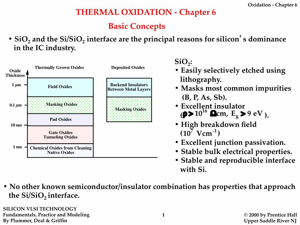
THERMAL OXIDATION - Chapter 6Basic Concepts
• SiO2 and the Si/SiO2 interface are the principal reasons for silicon’s dominance in the IC industry.
10 nm
0.1 µm
1 µm
1 nm
Masking Oxides
Gate OxidesTunneling Oxides
Field Oxides
Pad Oxides
Chemical Oxides from CleaningNative Oxides
Thermally Grown OxidesOxide
Thickness
Deposited Oxides
Backend InsulatorsBetween Metal Layers
Masking Oxides
SiO2:• Easily selectively etched using
lithography.• Masks most common impurities (B, P, As, Sb).• Excellent insulator ( ).• High breakdown field ( )• Excellent junction passivation.• Stable bulk electrical properties.• Stable and reproducible interface
with Si.
• No other known semiconductor/insulator combination has properties that approach the Si/SiO2 interface.
�
ρ > 1016 Ωcm, Eg > 9 eV
�
107 Vcm-1
Oxidation - Chapter 6
SILICON VLSI TECHNOLOGYFundamentals, Practice and ModelingBy Plummer, Deal & Griffin
© 2000 by Prentice HallUpper Saddle River NJ
2
1
1
1.3
11
1
1.2
1
1
1
1.3
1.3
Si substrate Si substrate
SiO2
Deposited Polysilicon
Si Substrate
Original Si SurfaceVolumeExpansion
Location of Si3N4 Mask
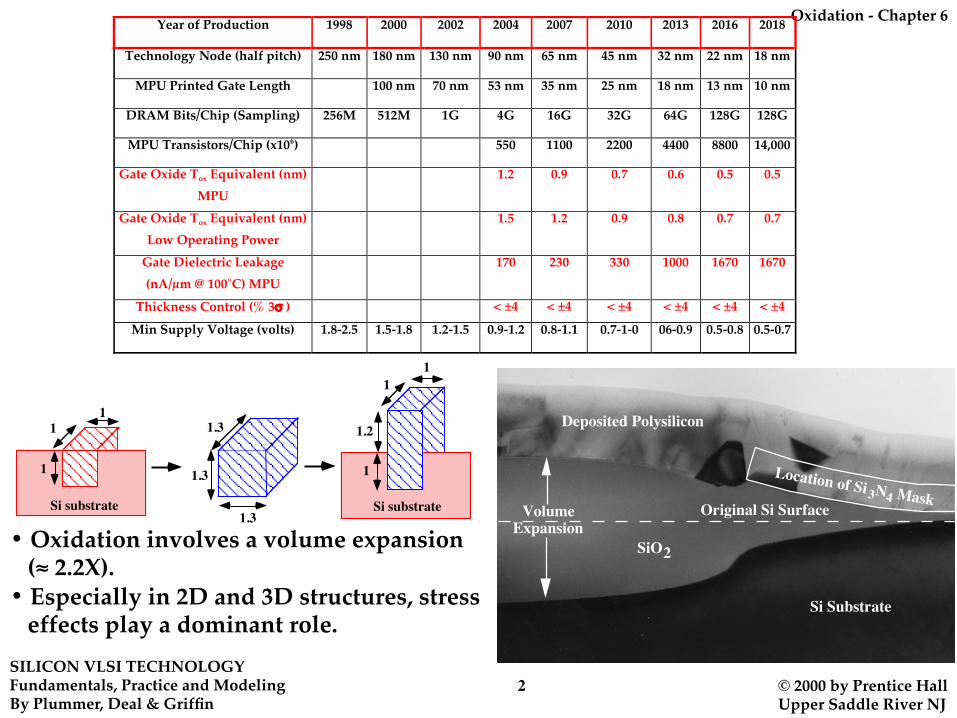
• Oxidation involves a volume expansion (≈ 2.2X).• Especially in 2D and 3D structures, stress effects play a dominant role.
Year of Production 1998 2000 2002 2004 2007 2010 2013 2016 2018
Technology Node (half pitch) 250 nm 180 nm 130 nm 90 nm 65 nm 45 nm 32 nm 22 nm 18 nm
MPU Printed Gate Length 100 nm 70 nm 53 nm 35 nm 25 nm 18 nm 13 nm 10 nm
DRAM Bits/Chip (Sampling) 256M 512M 1G 4G 16G 32G 64G 128G 128G
MPU Transistors/Chip (x106) 550 1100 2200 4400 8800 14,000
Gate Oxide Tox Equivalent (nm)MPU
1.2 0.9 0.7 0.6 0.5 0.5
Gate Oxide Tox Equivalent (nm)Low Operating Power
1.5 1.2 0.9 0.8 0.7 0.7
Gate Dielectric Leakage(nA/µm @ 100˚C) MPU
170 230 330 1000 1670 1670
Thickness Control (% 3σ ) < ±4 < ±4 < ±4 < ±4 < ±4 < ±4
Min Supply Voltage (volts) 1.8-2.5 1.5-1.8 1.2-1.5 0.9-1.2 0.8-1.1 0.7-1-0 06-0.9 0.5-0.8 0.5-0.7
Oxidation - Chapter 6
SILICON VLSI TECHNOLOGYFundamentals, Practice and ModelingBy Plummer, Deal & Griffin
© 2000 by Prentice HallUpper Saddle River NJ
3
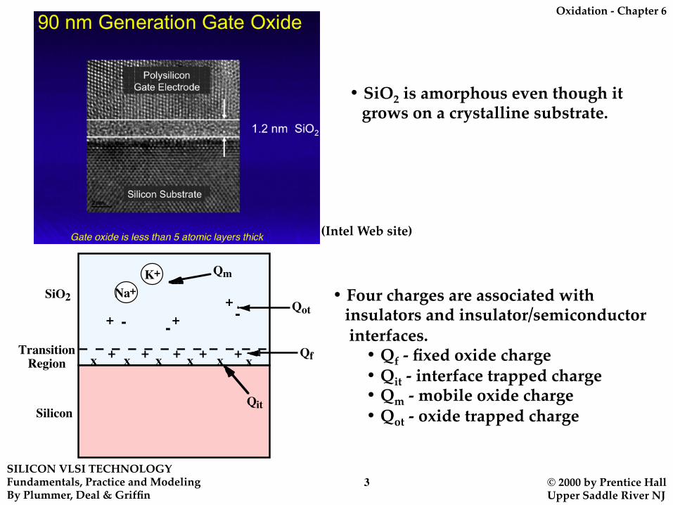
(Intel Web site)
• SiO2 is amorphous even though it grows on a crystalline substrate.
++++ + xxxxxx
+++ ---
K+
TransitionRegion
Na+SiO2
Qm
Qot
Qf
QitSilicon
• Four charges are associated with insulators and insulator/semiconductor interfaces. • Qf - fixed oxide charge • Qit - interface trapped charge • Qm - mobile oxide charge • Qot - oxide trapped charge
Oxidation - Chapter 6
SILICON VLSI TECHNOLOGYFundamentals, Practice and ModelingBy Plummer, Deal & Griffin
© 2000 by Prentice HallUpper Saddle River NJ
4
QuartzTube
Wafers
Quartz Carrier
Resistance Heating
H2O2
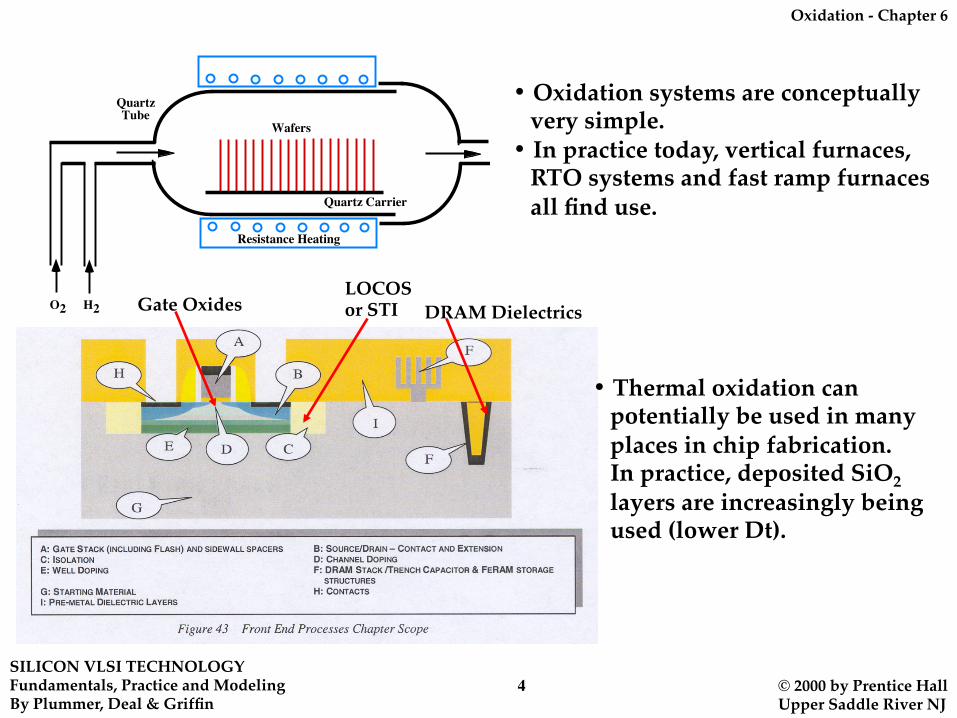
• Oxidation systems are conceptually very simple.• In practice today, vertical furnaces, RTO systems and fast ramp furnaces all find use.
• Thermal oxidation can potentially be used in many places in chip fabrication. In practice, deposited SiO2 layers are increasingly being used (lower Dt).
Gate OxidesLOCOSor STI DRAM Dielectrics
Oxidation - Chapter 6
SILICON VLSI TECHNOLOGYFundamentals, Practice and ModelingBy Plummer, Deal & Griffin
© 2000 by Prentice HallUpper Saddle River NJ
5
C
C
C
N SiliconDoping = ND
+ + + +++ +
+ + + ++ +++ +
+++ ++
Holes
a)
b)
c)
CO
CO
COCO
COCO
e-
e-
e-
CDxD
+ VG
- VG
-- VG
VG
VG
VG
+
+
+-
-
-
VTH
QG
QIQD CDMinxDMax
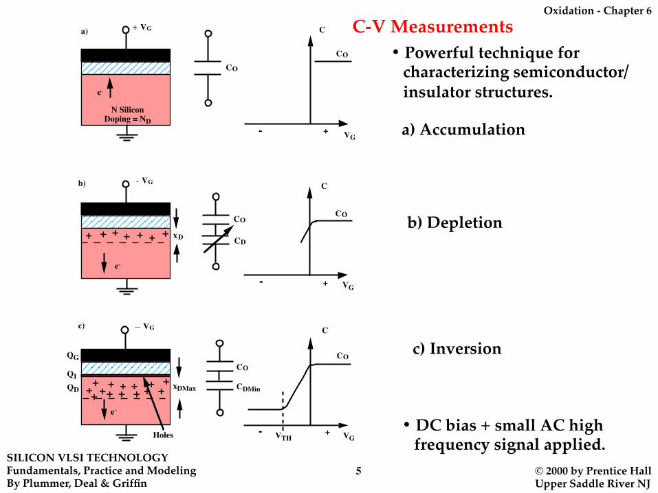
C-V Measurements• Powerful technique for characterizing semiconductor/ insulator structures.
a) Accumulation
b) Depletion
c) Inversion
• DC bias + small AC high frequency signal applied.
Oxidation - Chapter 6
SILICON VLSI TECHNOLOGYFundamentals, Practice and ModelingBy Plummer, Deal & Griffin
© 2000 by Prentice HallUpper Saddle River NJ
6
Ideal LF
Ideal HF
Deep Depletion
C
Cox
DC Gate VoltageVTH
CMin
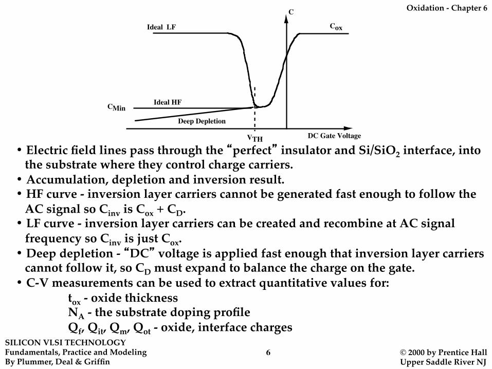
• Electric field lines pass through the “perfect” insulator and Si/SiO2 interface, into the substrate where they control charge carriers.• Accumulation, depletion and inversion result.• HF curve - inversion layer carriers cannot be generated fast enough to follow the AC signal so Cinv is Cox + CD.• LF curve - inversion layer carriers can be created and recombine at AC signal frequency so Cinv is just Cox.• Deep depletion - “DC” voltage is applied fast enough that inversion layer carriers cannot follow it, so CD must expand to balance the charge on the gate.• C-V measurements can be used to extract quantitative values for:
tox - oxide thickness NA - the substrate doping profile Qf, Qit, Qm, Qot - oxide, interface charges
Oxidation - Chapter 6
SILICON VLSI TECHNOLOGYFundamentals, Practice and ModelingBy Plummer, Deal & Griffin
© 2000 by Prentice HallUpper Saddle River NJ
7
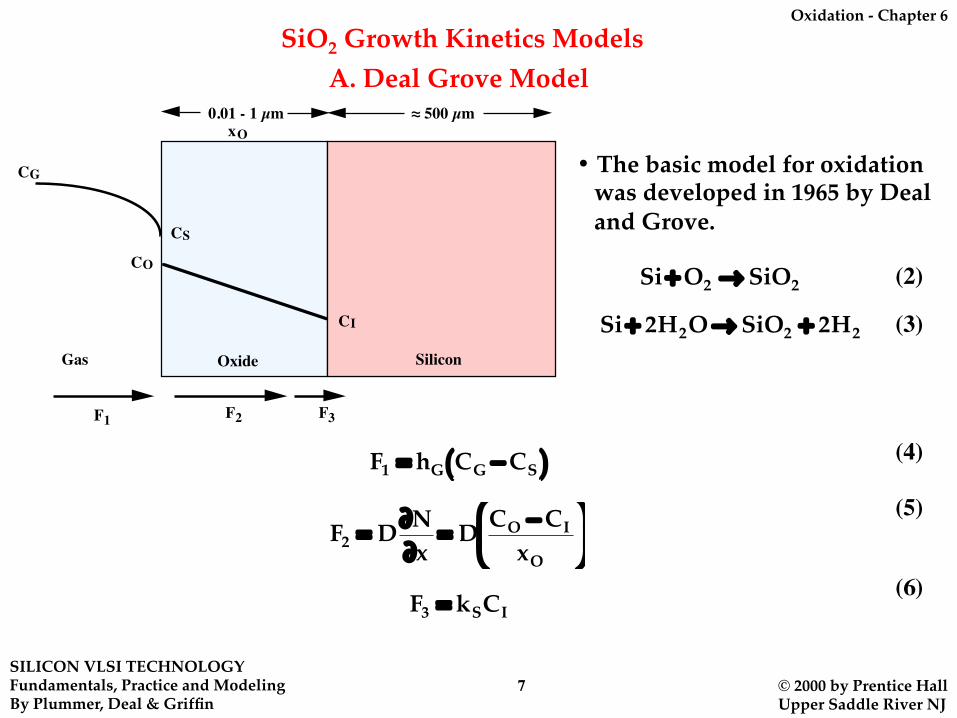
SiO2 Growth Kinetics ModelsA. Deal Grove Model
Oxide
CI
CG
CO
CS
CI
xO
Gas
0.01 - 1 µm ≈ 500 µm
Silicon
F1 F2 F3
• The basic model for oxidation was developed in 1965 by Deal and Grove.
�
Si + O2 → SiO2
�
Si + 2H2O→ SiO2 + 2H2
(2)
(3)
�
F1 = hG CG −CS( )
�
F2 = D∂N∂x
= D CO −CI
xO
⎛
⎝ ⎜
⎞
⎠ ⎟
�
F3 = kSCI
(4)
(5)
(6)
Oxidation - Chapter 6
SILICON VLSI TECHNOLOGYFundamentals, Practice and ModelingBy Plummer, Deal & Griffin
© 2000 by Prentice HallUpper Saddle River NJ
8
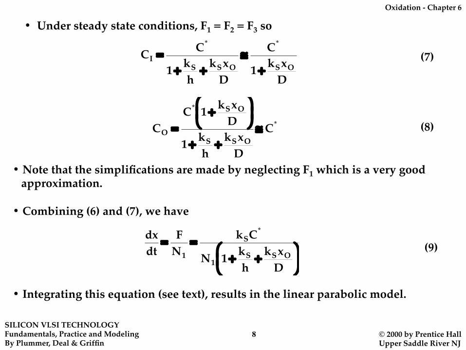
• Under steady state conditions, F1 = F2 = F3 so
�
CI = C*
1 + kS
h+ kSxO
D
≅ C*
1 + kSxO
D
(7)
�
CO =C* 1 + kSxO
D⎛ ⎝ ⎜
⎞ ⎠ ⎟
1 + kS
h+ kSxO
D
≅ C* (8)
• Note that the simplifications are made by neglecting F1 which is a very good approximation.
• Combining (6) and (7), we have
�
dxdt
= FN1
= kSC*
N1 1 + kS
h+ kSxO
D⎛ ⎝ ⎜
⎞ ⎠ ⎟
• Integrating this equation (see text), results in the linear parabolic model.
(9)
Oxidation - Chapter 6
SILICON VLSI TECHNOLOGYFundamentals, Practice and ModelingBy Plummer, Deal & Griffin
© 2000 by Prentice HallUpper Saddle River NJ
9
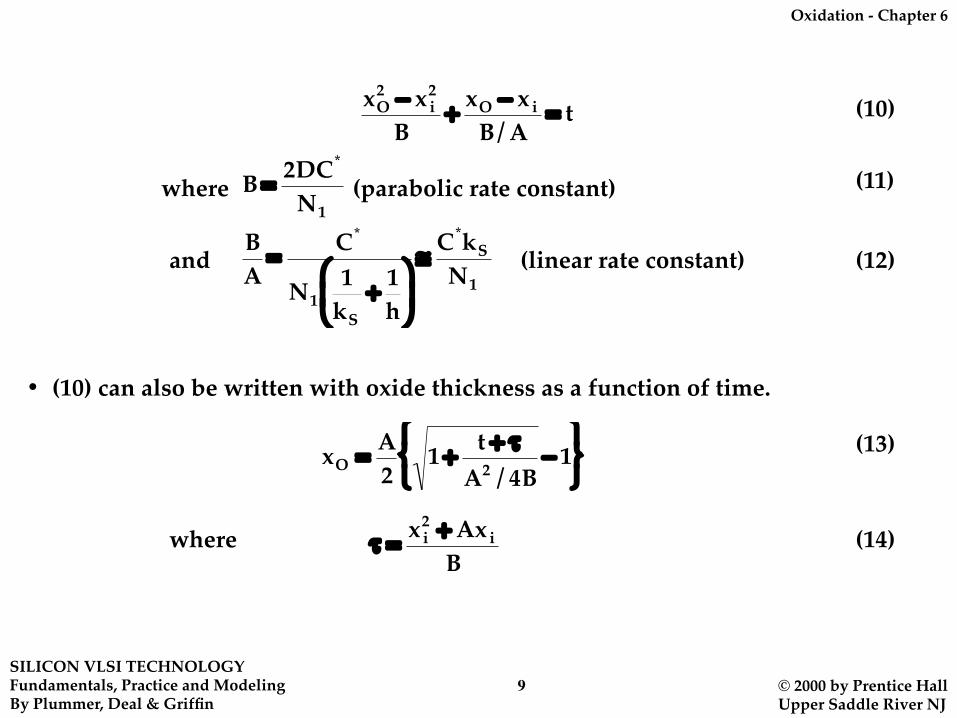
�
xO2 − x i
2
B+ xO − x i
B/ A= t (10)
where (parabolic rate constant)
�
B = 2DC*
N1(11)
(12)
�
BA
= C*
N11
kS+ 1
h⎛
⎝ ⎜
⎞
⎠ ⎟
≅ C*kSN1
(linear rate constant) and
• (10) can also be written with oxide thickness as a function of time.
�
xO = A2
1 + t + τA2 / 4B
− 1⎧ ⎨ ⎩
⎫ ⎬ ⎭
(13)
where
�
τ = x i2 + Ax i
B(14)
Oxidation - Chapter 6
SILICON VLSI TECHNOLOGYFundamentals, Practice and ModelingBy Plummer, Deal & Griffin
© 2000 by Prentice HallUpper Saddle River NJ
10
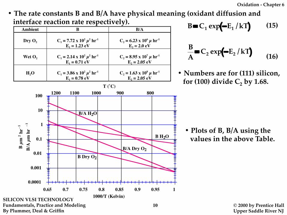
• The rate constants B and B/A have physical meaning (oxidant diffusion and interface reaction rate respectively).
�
B = C1 exp −E1 / kT( )
�
BA
= C2 exp −E2 / kT( )
(15)
(16)
Ambient B B/A
Dry O2 C1 = 7.72 x 10² µ2 hr-1
E1 = 1.23 eVC2 = 6.23 x 10⁶ µ hr-1
E2 = 2.0 eV
Wet O2 C1 = 2.14 x 10² µ2 hr-1
E1 = 0.71 eVC2 = 8.95 x 10⁷ µ hr-1
E2 = 2.05 eV
H2O C1 = 3.86 x 10² µ2 hr-1
E1 = 0.78 eVC2 = 1.63 x 10⁸ µ hr-1
E2 = 2.05 eV
.
0.0001
0.001
0.01
0.1
1
10
100
0.65 0.7 0.75 0.8 0.85 0.9 0.95 1
B µm
2hr
-1
B/A
µm
hr
-1
1000/T (Kelvin)
800900100011001200T (˚C)
B/A H2O
B/A Dry O2
B Dry O2
B H2O• Plots of B, B/A using the values in the above Table.
• Numbers are for (111) silicon, for (100) divide C2 by 1.68.
Oxidation - Chapter 6
SILICON VLSI TECHNOLOGYFundamentals, Practice and ModelingBy Plummer, Deal & Griffin
© 2000 by Prentice HallUpper Saddle River NJ
11
0
0.1
0.2
0.3
0.4
0.5
0.6
0.7
0 2 4 6 8 10
Oxi
de T
hick
ness
- m
icro
ns
Time - hours
1200˚C
1100˚C
1000˚C
900˚C800˚C
0
0.5
1
1.5
2
0 1 2 3 4 5 6 7 8 9 10
Oxi
de T
hick
ness
- m
icro
ns
Time - hours
1100 ˚C
700 ˚C
1000 ˚C
900 ˚C
800 ˚C
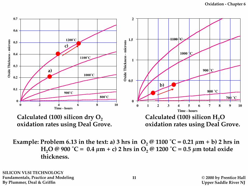
Calculated (100) silicon dry O2 oxidation rates using Deal Grove.
Calculated (100) silicon H2O oxidation rates using Deal Grove.
Example: Problem 6.13 in the text: a) 3 hrs in O2 @ 1100 ˚C = 0.21 µm + b) 2 hrs in H2O @ 900 ˚C = 0.4 µm + c) 2 hrs in O2 @ 1200 ˚C = 0.5 µm total oxide thickness.
a)
b)
c)
Oxidation - Chapter 6
SILICON VLSI TECHNOLOGYFundamentals, Practice and ModelingBy Plummer, Deal & Griffin
© 2000 by Prentice HallUpper Saddle River NJ
12
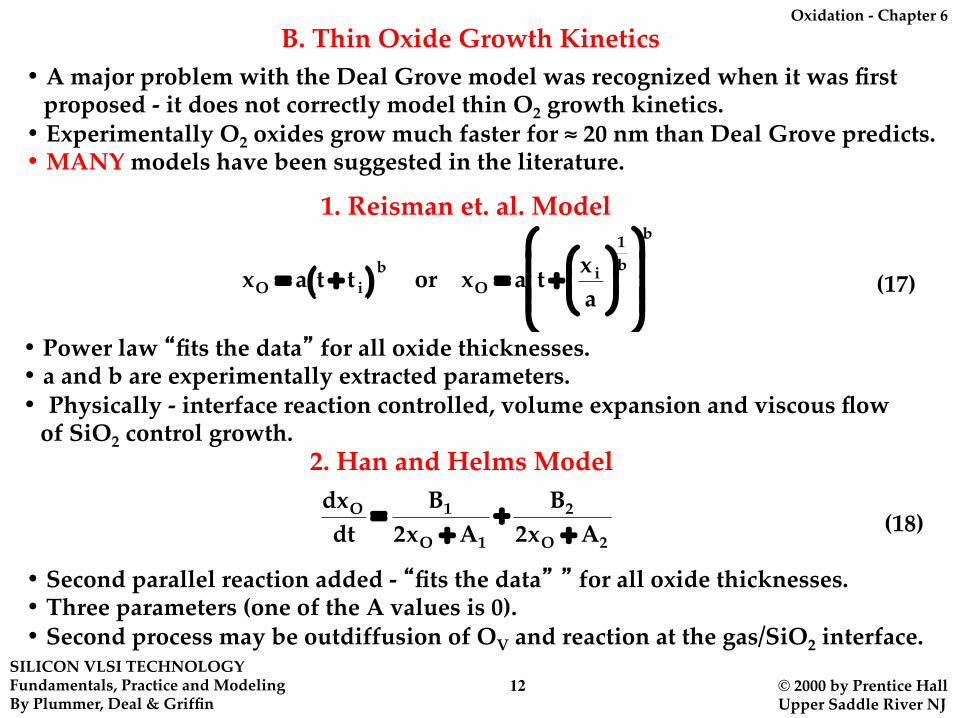
B. Thin Oxide Growth Kinetics• A major problem with the Deal Grove model was recognized when it was first proposed - it does not correctly model thin O2 growth kinetics.• Experimentally O2 oxides grow much faster for ≈ 20 nm than Deal Grove predicts.• MANY models have been suggested in the literature.
1. Reisman et. al. Model
�
xO = a t + t i( ) b or xO = a t + x i
a⎛ ⎝ ⎜
⎞ ⎠ ⎟
1b
⎛
⎝
⎜ ⎜ ⎜
⎞
⎠
⎟ ⎟ ⎟
b
(17)
• Power law “fits the data” for all oxide thicknesses.• a and b are experimentally extracted parameters.• Physically - interface reaction controlled, volume expansion and viscous flow of SiO2 control growth.
2. Han and Helms Model
�
dxO
dt= B1
2xO + A1+ B2
2xO + A2(18)
• Second parallel reaction added - “fits the data” ” for all oxide thicknesses.• Three parameters (one of the A values is 0).• Second process may be outdiffusion of OV and reaction at the gas/SiO2 interface.
Oxidation - Chapter 6
SILICON VLSI TECHNOLOGYFundamentals, Practice and ModelingBy Plummer, Deal & Griffin
© 2000 by Prentice HallUpper Saddle River NJ
13
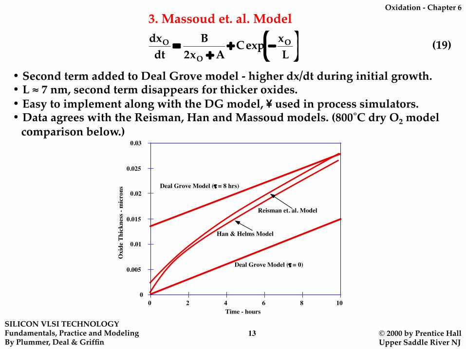
3. Massoud et. al. Model
�
dxO
dt= B
2xO + A+ Cexp − xO
L⎛ ⎝ ⎜
⎞ ⎠ ⎟ (19)
• Second term added to Deal Grove model - higher dx/dt during initial growth.• L ≈ 7 nm, second term disappears for thicker oxides.• Easy to implement along with the DG model, \ used in process simulators.• Data agrees with the Reisman, Han and Massoud models. (800˚C dry O2 model comparison below.)
.
0
0.005
0.01
0.015
0.02
0.025
0.03
0 2 4 6 8 10
Oxi
de T
hick
ness
- m
icro
ns
Han & Helms Model
Reisman et. al. Model
Time - hours
Deal Grove Model (τ = 0)
Deal Grove Model (τ = 8 hrs)
Oxidation - Chapter 6
SILICON VLSI TECHNOLOGYFundamentals, Practice and ModelingBy Plummer, Deal & Griffin
© 2000 by Prentice HallUpper Saddle River NJ
14
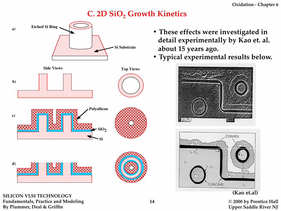
C. 2D SiO2 Growth KineticsEtched Si Ring
Si Substrate
Side Views Top Views
Polysilicon
SiO2
Si
a)
b)
c)
d)
• These effects were investigated in detail experimentally by Kao et. al. about 15 years ago.• Typical experimental results below.
(Kao et.al)
Oxidation - Chapter 6
SILICON VLSI TECHNOLOGYFundamentals, Practice and ModelingBy Plummer, Deal & Griffin
© 2000 by Prentice HallUpper Saddle River NJ
15
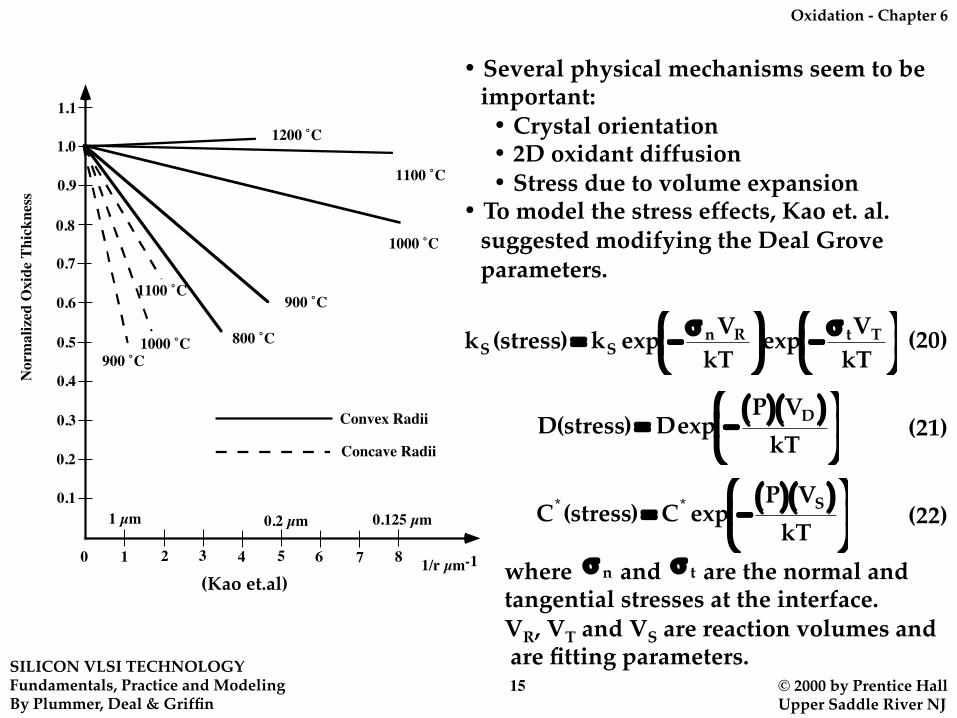
.
0 1 2 3 4 5 6 7 8 1/r µm-1
0.1
0.2
0.3
0.4
0.5
0.6
0.7
0.8
0.9
1.0
1.1
Nor
mal
ized
Oxi
de T
hick
ness
Convex Radii
Concave Radii
1200 ˚C
1100 ˚C
1000 ˚C
900 ˚C
800 ˚C
1100 ˚C
1000 ˚C900 ˚C
1 µm 0.2 µm 0.125 µm
• Several physical mechanisms seem to be important: • Crystal orientation • 2D oxidant diffusion • Stress due to volume expansion• To model the stress effects, Kao et. al. suggested modifying the Deal Grove parameters.
�
kS (stress) = kS exp − σ nVR
kT⎛ ⎝ ⎜
⎞ ⎠ ⎟ exp − σ tVT
kT⎛ ⎝ ⎜
⎞ ⎠ ⎟
�
D(stress) = Dexp −P( ) VD( )
kT
⎛
⎝ ⎜
⎞
⎠ ⎟
�
C*(stress) = C* exp −P( ) VS( )
kT
⎛
⎝ ⎜
⎞
⎠ ⎟
(20)
(22)
(21)
where and are the normal and tangential stresses at the interface. VR, VT and VS are reaction volumes and are fitting parameters.
(Kao et.al)
�
σ n
�
σ t
Oxidation - Chapter 6
SILICON VLSI TECHNOLOGYFundamentals, Practice and ModelingBy Plummer, Deal & Griffin
© 2000 by Prentice HallUpper Saddle River NJ
16
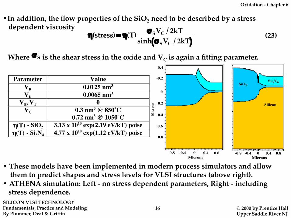
•In addition, the flow properties of the SiO2 need to be described by a stress dependent viscosity
�
η(stress) = η(T) σSVC / 2kTsinh σSVC / 2kT( ) (23)
Where is the shear stress in the oxide and VC is again a fitting parameter.
�
σS
Parameter ValueVR 0.0125 nm3
VD 0.0065 nm3
VS, VT 0VC 0.3 nm3 @ 850˚C
0.72 nm3 @ 1050˚Cη(T) - SiO2 3.13 x 10¹⁰ exp(2.19 eV/kT) poiseη(T) - Si3N4 4.77 x 10¹⁰ exp(1.12 eV/kT) poise
• These models have been implemented in modern process simulators and allow them to predict shapes and stress levels for VLSI structures (above right).• ATHENA simulation: Left - no stress dependent parameters, Right - including stress dependence.
.
Silicon
SiO2Si3N4
0
0.2
0.4
0.6
0.8
-0.2
-0.4
MicronsMicrons
0 0.4 0.8-0.4-0.8Microns0 0.4 0.8-0.4-0.8
Oxidation - Chapter 6
SILICON VLSI TECHNOLOGYFundamentals, Practice and ModelingBy Plummer, Deal & Griffin
© 2000 by Prentice HallUpper Saddle River NJ
17
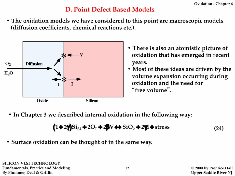
D. Point Defect Based Models• The oxidation models we have considered to this point are macroscopic models (diffusion coefficients, chemical reactions etc.).
*
*O2
H2O
Diffusion
Oxide Silicon
II
V
�
1 + 2γ( )SiSi + 2OI + 2βV↔ SiO2 + 2γI + stress
• There is also an atomistic picture of oxidation that has emerged in recent years.• Most of these ideas are driven by the volume expansion occurring during oxidation and the need for “free volume”.
• In Chapter 3 we described internal oxidation in the following way:
(24)
• Surface oxidation can be thought of in the same way.
Oxidation - Chapter 6
SILICON VLSI TECHNOLOGYFundamentals, Practice and ModelingBy Plummer, Deal & Griffin
© 2000 by Prentice HallUpper Saddle River NJ
18
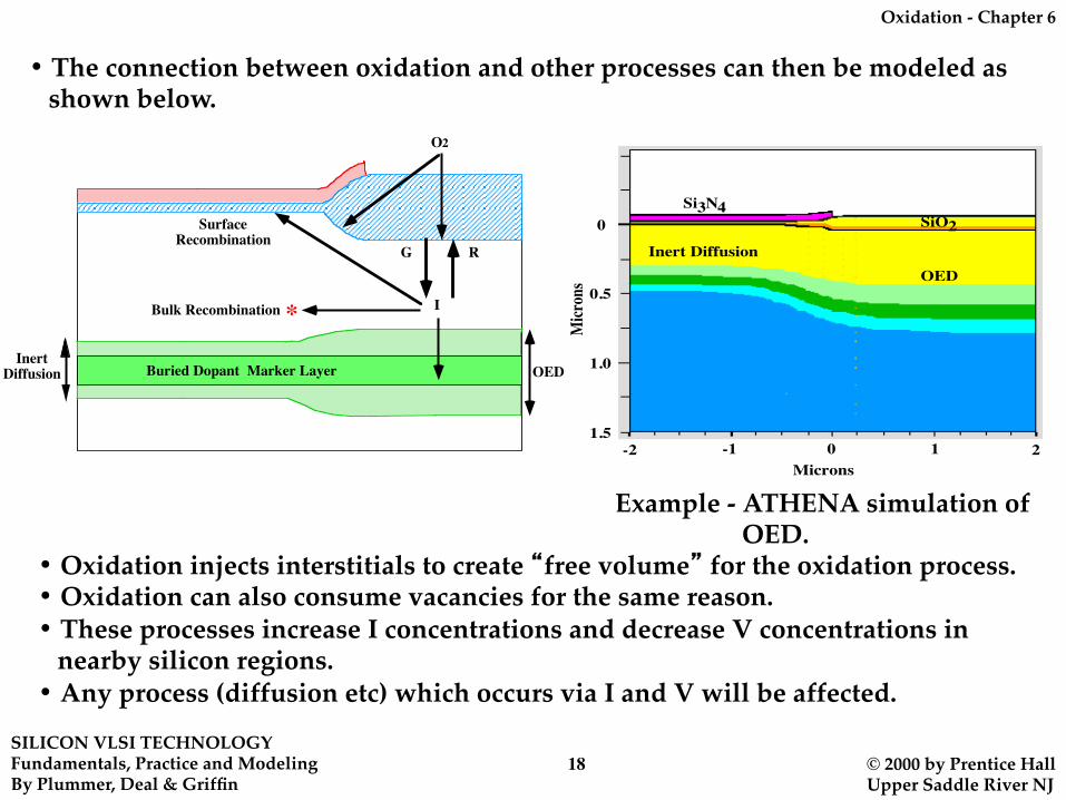
• The connection between oxidation and other processes can then be modeled as shown below.
Buried Dopant Marker Layer
G R
Bulk Recombination
SurfaceRecombination
*
OEDInert
Diffusion
O2
I
.
Inert DiffusionOED
Micr
ons
0
0.5
1.0
1.5
Microns0 1 2-1-2
Si3N4SiO2
Example - ATHENA simulation of OED.
• Oxidation injects interstitials to create “free volume” for the oxidation process.• Oxidation can also consume vacancies for the same reason.• These processes increase I concentrations and decrease V concentrations in nearby silicon regions.• Any process (diffusion etc) which occurs via I and V will be affected.
Oxidation - Chapter 6
SILICON VLSI TECHNOLOGYFundamentals, Practice and ModelingBy Plummer, Deal & Griffin
© 2000 by Prentice HallUpper Saddle River NJ
19
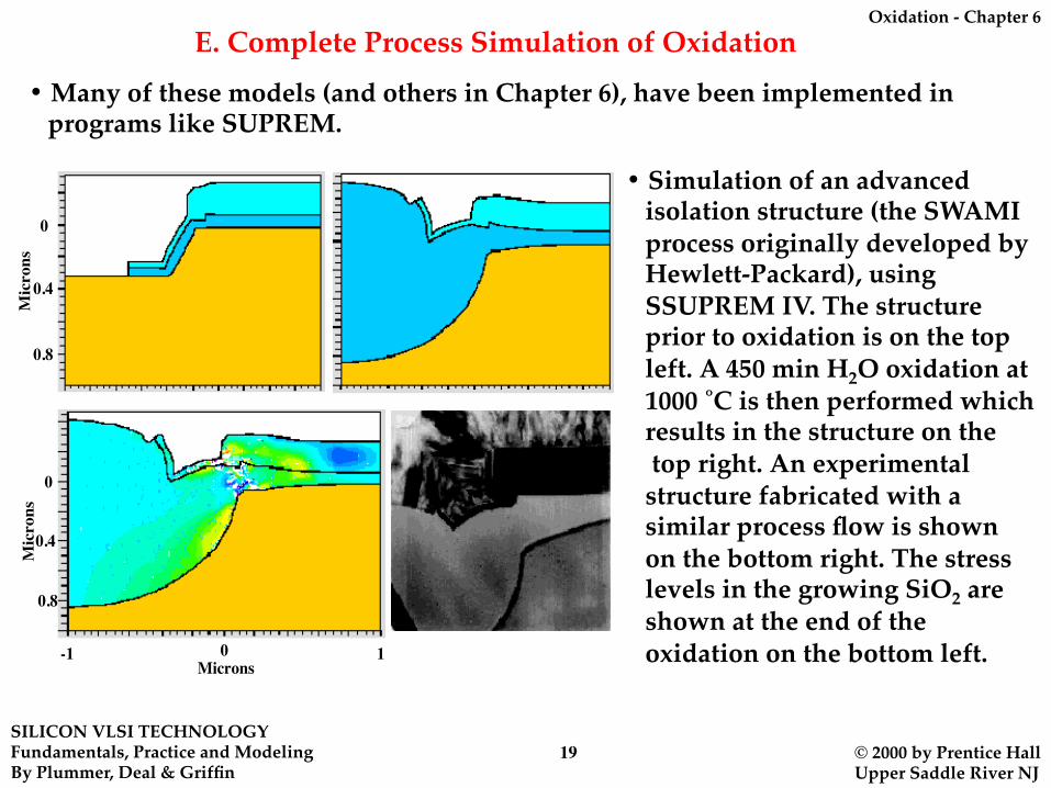
E. Complete Process Simulation of Oxidation• Many of these models (and others in Chapter 6), have been implemented in programs like SUPREM.
.
0
0.4
0.8
Microns
0
0.4
0.8
Microns
Microns1-1 0
• Simulation of an advanced isolation structure (the SWAMI process originally developed by Hewlett-Packard), using SSUPREM IV. The structure prior to oxidation is on the top left. A 450 min H2O oxidation at 1000 ˚C is then performed which results in the structure on the top right. An experimental structure fabricated with a similar process flow is shown on the bottom right. The stress levels in the growing SiO2 are shown at the end of the oxidation on the bottom left.
Oxidation - Chapter 6
SILICON VLSI TECHNOLOGYFundamentals, Practice and ModelingBy Plummer, Deal & Griffin
© 2000 by Prentice HallUpper Saddle River NJ
20
Summary of Key Ideas
• Thermal oxidation has been a key element of silicon technology since its inception.
• Thermally, chemically, mechanically and electrically stable SiO2 layers on silicon distinguish silicon from other possible semiconductors.
• The basic growth kinetics of SiO2 on silicon are controlled by oxidant diffusion and Si/SiO2 interface chemical reaction.
• This simple Deal-Grove model has been extended to include 2D effects, high dopant concentrations, mixed ambients and thin oxides.
• Oxidation can also have long range effects on dopant diffusion (OED or ORD) which are modeled through point defect interactions.
• Process simulators today include all these physical effects (and more) and are quite powerful in predicting oxidation geometry and properties.