Embed Size (px)
Citation preview
Chapter 2
D-MOSFET Structure
The first power MOSFET structure commercially introduced by the power semi-
conductor industry was the double-diffused or D-MOSFET structure. The channel
length of this device could be reduced to sub-micron dimensions by controlling the
diffusion depths of the P-base and N+ source regions without resorting to expensive
lithography tools [1]. The device fabrication process relied up on the available
planar gate technology used to manufacture CMOS integrated circuits. These
devices found applications in power electronic circuits that operated at low
(<100 V) voltages. The fast switching speed and ruggedness of the D-MOSFET
structure were significant advantages compared with the performance of the avail-
able bipolar power transistor.
The physics of operation of the power D-MOSFET structure has been analyzed
in detail in the textbook [1]. In this chapter of the monograph, a brief description of
the device operation is provided for completeness and for contrasting it to the
advanced device structures that are discussed in later chapters. However, a detailed
discussion of the characteristics of a device rated for blocking 30 V is provided here
based up on the results of two-dimensional numerical simulations. These charac-
teristics will be used as a bench-mark for comparison with the characteristics of the
advanced power MOSFET structures described in other chapters.
2.1 The D-MOSFET Structure
A cross-section of the basic cell structure for the D-MOSFET structure is illustrated
in Fig. 2.1. This device structure is fabricated by starting with an N-type epitaxial
layer grown on a heavily doped Nþ substrate. The channel is formed by the
difference in lateral extension of the P-base and Nþ source regions produced by
their diffusion cycles. Both regions are self-aligned to the left-hand-side and right-
hand-side of the gate region during ion-implantation to introduce the respective
dopants. A refractory gate electrode, such as polysilicon, is required to allow
diffusion of the dopants under the gate electrode at elevated temperatures.
B.J. Baliga, Advanced Power MOSFET Concepts,DOI 10.1007/978-1-4419-5917-1_2, # Springer ScienceþBusiness Media, LLC 2010
23
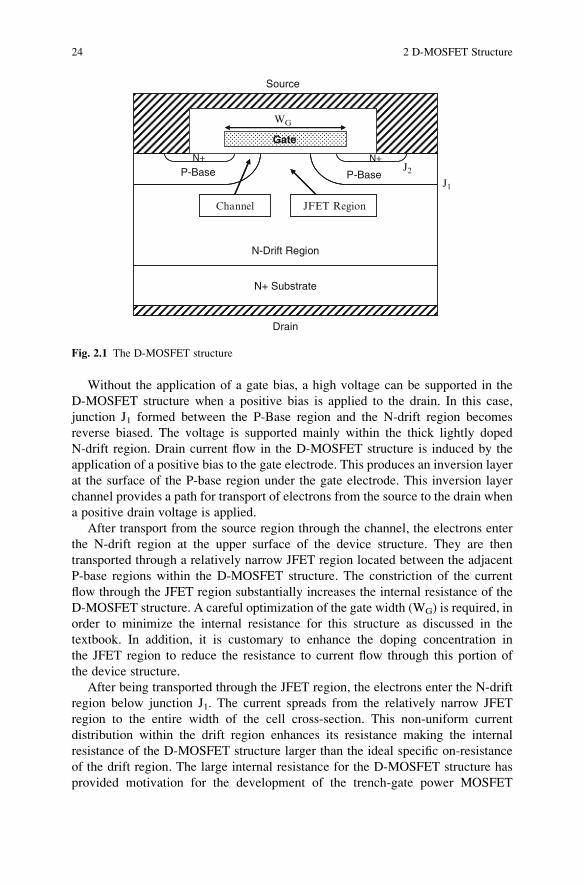
Without the application of a gate bias, a high voltage can be supported in the
D-MOSFET structure when a positive bias is applied to the drain. In this case,
junction J1 formed between the P-Base region and the N-drift region becomes
reverse biased. The voltage is supported mainly within the thick lightly doped
N-drift region. Drain current flow in the D-MOSFET structure is induced by the
application of a positive bias to the gate electrode. This produces an inversion layer
at the surface of the P-base region under the gate electrode. This inversion layer
channel provides a path for transport of electrons from the source to the drain when
a positive drain voltage is applied.
After transport from the source region through the channel, the electrons enter
the N-drift region at the upper surface of the device structure. They are then
transported through a relatively narrow JFET region located between the adjacent
P-base regions within the D-MOSFET structure. The constriction of the current
flow through the JFET region substantially increases the internal resistance of the
D-MOSFET structure. A careful optimization of the gate width (WG) is required, in
order to minimize the internal resistance for this structure as discussed in the
textbook. In addition, it is customary to enhance the doping concentration in
the JFET region to reduce the resistance to current flow through this portion of
the device structure.
After being transported through the JFET region, the electrons enter the N-drift
region below junction J1. The current spreads from the relatively narrow JFET
region to the entire width of the cell cross-section. This non-uniform current
distribution within the drift region enhances its resistance making the internal
resistance of the D-MOSFET structure larger than the ideal specific on-resistance
of the drift region. The large internal resistance for the D-MOSFET structure has
provided motivation for the development of the trench-gate power MOSFET
Source
P-Base
Gate
N+ N+
J1
WG
N+ Substrate
N-Drift Region
P-Base
Drain
Channel
J2
JFET Region
Fig. 2.1 The D-MOSFET structure
24 2 D-MOSFET Structure
structure in the 1990s and the advanced power MOSFET structures discussed in this
monograph.
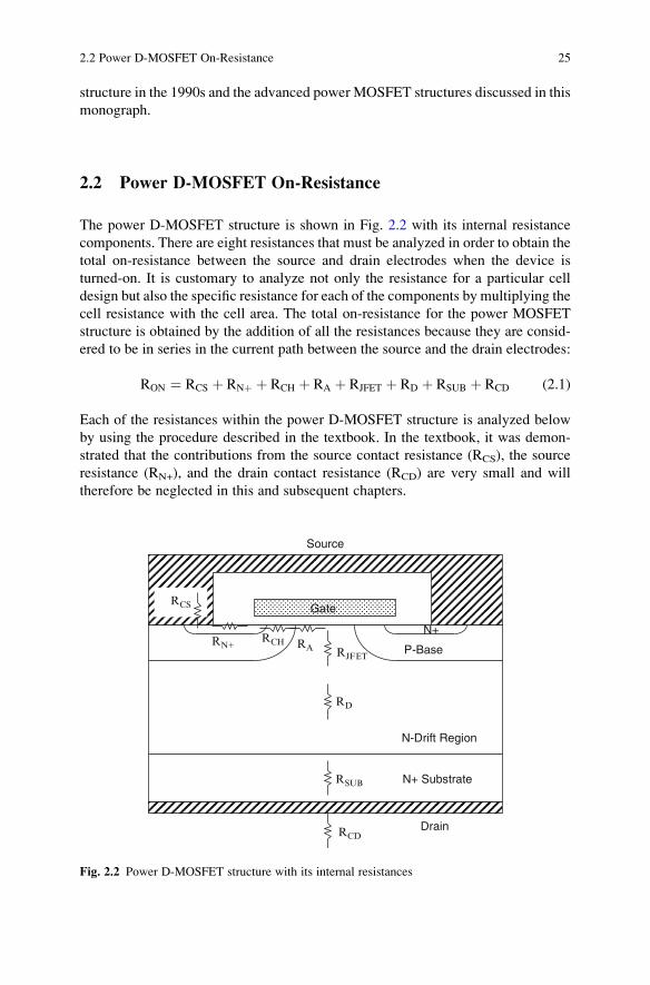
2.2 Power D-MOSFET On-Resistance
The power D-MOSFET structure is shown in Fig. 2.2 with its internal resistance
components. There are eight resistances that must be analyzed in order to obtain the
total on-resistance between the source and drain electrodes when the device is
turned-on. It is customary to analyze not only the resistance for a particular cell
design but also the specific resistance for each of the components by multiplying the
cell resistance with the cell area. The total on-resistance for the power MOSFET
structure is obtained by the addition of all the resistances because they are consid-
ered to be in series in the current path between the source and the drain electrodes:
RON ¼ RCS þ RNþ þ RCH þ RA þ RJFET þ RD þ RSUB þ RCD (2.1)
Each of the resistances within the power D-MOSFET structure is analyzed below
by using the procedure described in the textbook. In the textbook, it was demon-
strated that the contributions from the source contact resistance (RCS), the source
resistance (RN+), and the drain contact resistance (RCD) are very small and will
therefore be neglected in this and subsequent chapters.
N+ Substrate
N-Drift Region
Drain
Source
P-Base
N+RCH RA RJFET
RD
RSUB
RCD
RCS
RN+
Gate
Fig. 2.2 Power D-MOSFET structure with its internal resistances
2.2 Power D-MOSFET On-Resistance 25
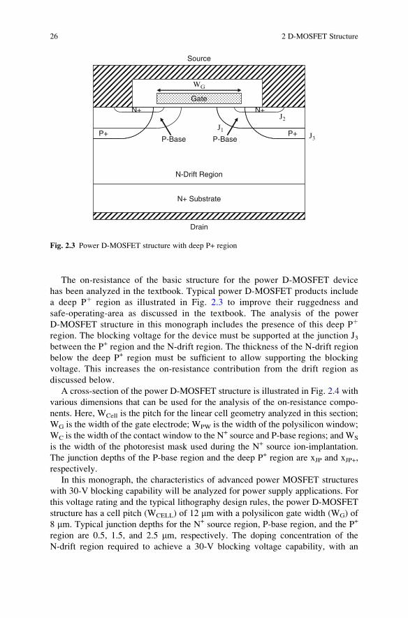
The on-resistance of the basic structure for the power D-MOSFET device
has been analyzed in the textbook. Typical power D-MOSFET products include
a deep Pþ region as illustrated in Fig. 2.3 to improve their ruggedness and
safe-operating-area as discussed in the textbook. The analysis of the power
D-MOSFET structure in this monograph includes the presence of this deep Pþ
region. The blocking voltage for the device must be supported at the junction J3between the P+ region and the N-drift region. The thickness of the N-drift region
below the deep P+ region must be sufficient to allow supporting the blocking
voltage. This increases the on-resistance contribution from the drift region as
discussed below.
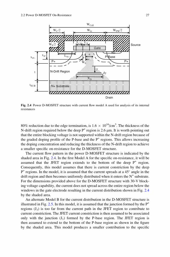
A cross-section of the power D-MOSFET structure is illustrated in Fig. 2.4 with
various dimensions that can be used for the analysis of the on-resistance compo-
nents. Here, WCell is the pitch for the linear cell geometry analyzed in this section;
WG is the width of the gate electrode; WPW is the width of the polysilicon window;
WC is the width of the contact window to the N+ source and P-base regions; and WS
is the width of the photoresist mask used during the N+ source ion-implantation.
The junction depths of the P-base region and the deep P+ region are xJP and xJP+,
respectively.
In this monograph, the characteristics of advanced power MOSFET structures
with 30-V blocking capability will be analyzed for power supply applications. For
this voltage rating and the typical lithography design rules, the power D-MOSFET
structure has a cell pitch (WCELL) of 12 mm with a polysilicon gate width (WG) of
8 mm. Typical junction depths for the N+ source region, P-base region, and the P+
region are 0.5, 1.5, and 2.5 mm, respectively. The doping concentration of the
N-drift region required to achieve a 30-V blocking voltage capability, with an
N+ Substrate
N-Drift Region
P-Base
Drain
Source
P-Base
N+ N+
J1
J2
WG
P+ P+ J3
Gate
Fig. 2.3 Power D-MOSFET structure with deep P+ region
26 2 D-MOSFET Structure
80% reduction due to the edge termination, is 1.6 � 1016/cm3. The thickness of the
N-drift region required below the deep P+ region is 2.6 mm. It is worth pointing out
that the entire blocking voltage is not supported within the N-drift region because of
the graded doping profile of the P-base and the P+ regions. This allows increasing
the doping concentration and reducing the thickness of the N-drift region to achieve
a smaller specific on-resistance for the D-MOSFET structure.
The current flow pattern in the power D-MOSFET structure is indicated by the
shaded area in Fig. 2.4. In the first Model A for the specific on-resistance, it will be
assumed that the JFET region extends to the bottom of the deep P+ region.
Consequently, this model assumes that there is current constriction by the deep
P+ regions. In the model, it is assumed that the current spreads at a 45� angle in the
drift region and then becomes uniformly distributed when it enters the N+ substrate.
For the dimensions provided above for the D-MOSFET structure with 30-V block-
ing voltage capability, the current does not spread across the entire region below the
windows in the gate electrode resulting in the current distribution shown in Fig. 2.4
by the shaded area.
An alternate Model B for the current distribution in the D-MOSFET structure is
illustrated in Fig. 2.5. In this model, it is assumed that the junction formed by the P+
regions (J3) is too far from the current path in the JFET region to contribute to
current constriction. The JFET current constriction is then assumed to be associated
only with the junction (J1) formed by the P-base region. The JFET region is
then assumed to extend to the bottom of the P-base region as shown in the figure
by the shaded area. This model produces a smaller contribution to the specific
N-Drift Region
Drain
Source
P-Base
Gate
N+
N+ Substrate
WGWC/2 WPW/2
WCell
a
ydy
XD
t
W0
xJP LN+
tSUB
LCHWS/2LA
P+ P+xJP+
Fig. 2.4 Power D-MOSFET structure with current flow model A used for analysis of its internal
resistances
2.2 Power D-MOSFET On-Resistance 27
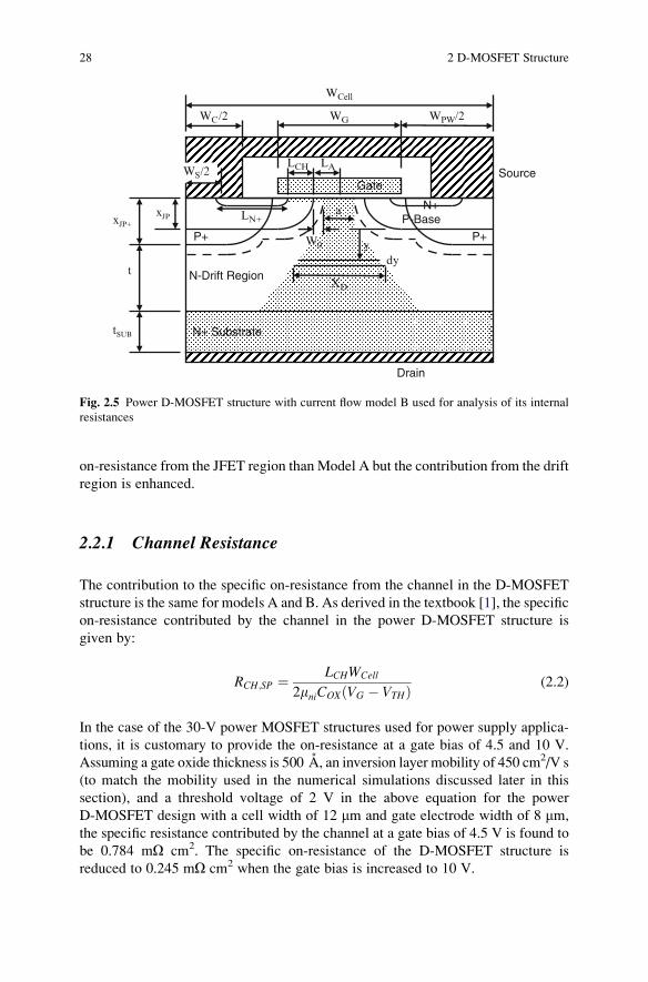
on-resistance from the JFET region than Model A but the contribution from the drift
region is enhanced.
2.2.1 Channel Resistance
The contribution to the specific on-resistance from the channel in the D-MOSFET
structure is the same for models A and B. As derived in the textbook [1], the specific
on-resistance contributed by the channel in the power D-MOSFET structure is
given by:
RCH;SP ¼ LCHWCell
2mniCOX VG � VTHð Þ (2.2)
In the case of the 30-V power MOSFET structures used for power supply applica-
tions, it is customary to provide the on-resistance at a gate bias of 4.5 and 10 V.
Assuming a gate oxide thickness is 500 A, an inversion layer mobility of 450 cm2/V s
(to match the mobility used in the numerical simulations discussed later in this
section), and a threshold voltage of 2 V in the above equation for the power
D-MOSFET design with a cell width of 12 mm and gate electrode width of 8 mm,
the specific resistance contributed by the channel at a gate bias of 4.5 V is found to
be 0.784 mO cm2. The specific on-resistance of the D-MOSFET structure is
reduced to 0.245 mO cm2 when the gate bias is increased to 10 V.
N-Drift Region
Drain
Source
P-Base
Gate
N+
N+ Substrate
WGWC/2 WPW/2
WCell
a
ydy
XD
t
W0
xJP LN+
tSUB
LCHWS/2LA
P+ P+xJP+
Fig. 2.5 Power D-MOSFET structure with current flow model B used for analysis of its internal
resistances
28 2 D-MOSFET Structure
2.2.2 Accumulation Resistance
In the power MOSFET structure, the current flowing through the inversion channel
enters the drift region at the edge of the P-base junction. The current then spreads
from the edge of the P-base junction into the JFET region. The current spreading
phenomenon is aided by the formation of an accumulation layer in the semicon-
ductor below the gate oxide due to the positive gate bias applied to turn-on the
device. The specific on-resistance contributed by the accumulation layer in the
power D-MOSFET structure is given by [1]:
RA;SP ¼ KAWG � 2xJPð ÞWCell
4mnACOX VG � VTHð Þ (2.3)
In writing this expression, a coefficient KA has been introduced to account for the
current spreading from the accumulation layer into the JFET region. A typical value
for this coefficient is 0.6 based upon the current flow observed from numerical
simulations of power D-MOSFET structures. The threshold voltage in the expres-
sion is for the on-set of formation of the accumulation layer. A zero threshold
voltage will be assumed here when performing the analytical computations. Note
that the junction depth of the P-base region (and not the P+ region) defines the
length of the accumulation region.
For the 30-V power D-MOSFET design with a cell width of 12 mm and gate
width of 8 mm, the specific resistance contributed by the accumulation layer at
a gate bias of 4.5 V is 0.294 mO cm2 if the P-base junction depth (xJP) is 1.5 mmand the gate oxide thickness is 500 A. An accumulation layer mobility of
1,000 cm2/V s was used in this calculation to match the mobility used in the
numerical simulations (discussed later in this section). When the gate bias is
increased to 10 V, the specific resistance contributed by the accumulation layer
is reduced to 0.132 mO cm2.
2.2.3 JFET Resistance
The electrons entering from the channel into the drift region are distributed into the
JFET region via the accumulation layer formed under the gate electrode. The
spreading of current in this region was accounted for by using a constant KA of
0.6 for the accumulation layer resistance. Consequently, the current flow through
the JFET region can be treated with a uniform current density. In the power
D-MOSFET structure, the cross-sectional area for the JFET region increases with
distance below the semiconductor surface due to the planar shape of the P-base
junction. However, in order to simplify the analysis, a uniform cross-section for the
current flow with a width ‘a’ will be assumed for the JFET region as illustrated by
2.2 Power D-MOSFET On-Resistance 29
the shaded area in Figs. 2.4 and 2.5. The width of the current flow is related to the
device structural parameters:
a ¼ WG � 2xJP � 2W0ð Þ (2.4)
where W0 is the zero-bias depletion width for the JFET region. The depletion region
boundary is indicated in the figures with the dashed lines. In the models, it is
assumed that no current can flow through the depleted region because all the free
carriers have been swept out by the prevailing electric field across the junction. The
zero-bias depletion width (W0) in the JFET region can be computed by using the
doping concentrations on both sides of the junction:
W0 ¼ffiffiffiffiffiffiffiffiffiffiffiffiffiffiffiffiffiffiffiffiffiffiffiffiffiffiffiffiffiffiffiffiffi
2eSNAVbi
qNDJ NA þ NDJð Þ
s(2.5)
where NA is the doping concentration in the P-base region and NDJ is the doping
concentration in the JFET region. In the above equation, the built-in potential is also
related to the doping concentrations on both sides of the junction:
Vbi ¼ kT
qln
NANDJ
n2i
� �(2.6)
In practical devices, the P-base region is diffused into the N-drift region produc-
ing a graded doping profile. However, these expressions based upon assuming
a uniform doping concentration for the P-base region are adequate for analyti-
cal computations. It is common practice to enhance the doping concentration
for the JFET region above that for the drift region. It is therefore appropriate to
use the enhanced doping concentration (NDJ) of the JFET region in the above
expressions.
In Model A, the JFET region is assumed to extend to the bottom the P+ region.
The specific on-resistance contributed by the JFET region in the power D-MOSFET
structure can then be obtained by using:
RJFET;SP ¼ rJFETxJPþWCell
WG � 2xJP � 2W0ð Þ (2.7)
where rJFET is the resistivity of the JFET region given by:
rJFET ¼ 1
qmnNDJ(2.8)
where mn is the bulk mobility appropriate to the doping level of the JFET region.
Typical power D-MOSFET structures are fabricated by using a diffused JFET
doping profile with its maximum concentration at the surface and a depth
30 2 D-MOSFET Structure

approximately the same as the junction depth of the P-base region. In an analytical
model, it is convenient to use an average doping concentration for the JFET region.
The resistivity for the JFET region is found to be 0.269 O cm corresponding to an
average JFET doping concentration of 2.0 � 1016/cm3. The zero-bias depletion
width in the JFET region for this JFET doping concentration is 0.228 mm. For the
30-V power D-MOSFET design with a cell width of 12 mm and gate width of 8 mm,
the specific resistance contributed by the JFET region is found to be 0.178 mO cm2
based up on using the above parameters.
In Model B, the JFET region is assumed to extend to the bottom the P-base
region. The specific on-resistance contributed by the JFET region in the power
D-MOSFET structure can then be obtained by using:
RJFET;SP ¼ rJFETxJPWCell
WG � 2xJP � 2W0ð Þ (2.9)
For the 30-V power D-MOSFET design with a cell width of 12 mm and gate width
of 8 mm, the specific resistance contributed by the JFET region is found to be
0.107 mO cm2 based up on using the same parameters as for Model A. It can
be observed that the JFET resistance is smaller in Model B than for Model A due to
the shorter path for current flow in the vertical direction.
2.2.4 Drift Region Resistance
The resistance contributed by the drift region in the power D-MOSFET structure is
enhanced well above that for the ideal drift region due to current spreading from the
JFET region. The cross-sectional area for the current flow in the drift region
increases from the width ‘a’ of the JFET region as illustrated in Figs. 2.4 and 2.5
by the shaded area. Several models for this current spreading have been proposed in
the literature [2]. The current distribution model used in this monograph is based up
on a spreading angle of 45�.In the case of Model A, the current spreads from the bottom of the P+ region as
shown in Fig. 2.4. The specific on-resistance contributed by the drift region in the
power D-MOSFET structure with this model is given by:
RD;SP ¼ rDWCell
2ln
aþ 2t
a
� �(2.10)
For the parameters given above for this structure, the dimension ‘a’ in the equation
is found to be 2.54 mm. For the 30-V power MOSFET design with a cell width of
12 mm and gate width of 8 mm, the specific resistance contributed by the drift region
is then found to be 0.149 mO cm2 by using a resistivity of the drift region of
0.325 O cm based upon a doping concentration of 1.6 � 1016/cm3.
2.2 Power D-MOSFET On-Resistance 31
In the case of Model B, the current spreads from the bottom of the P-base region
as shown in Fig. 2.5. The specific on-resistance contributed by the drift region in the
power D-MOSFET structure with this model is given by:
RD;SP ¼ rDWCell
2ln
aþ 2 tþ xJPþ�xJPð Þ½ �a
� �(2.11)
For the parameters given above for the 30-V power MOSFET design with a cell
width of 12 mm and gate width of 8 mm, the specific resistance contributed by the
drift region is then found to be 0.185 mO cm2 by using a resistivity of the drift
region of 0.325 O cm based upon a doping concentration of 1.6 � 1016/cm3.
Consequently, the drift region resistance contribution is larger for Model B than
for Model A.
2.2.5 N+ Substrate Resistance
When the current reaches the bottomof theN-drift region, it is very quickly distributed
throughout the heavily doped N+ substrate. The current flow through the substrate
can therefore be assumed to occur with a uniform cross-sectional area. Under this
assumption, the specific resistance contributed by the N+ substrate is given by:
RSUB;SP ¼ rSUBtSUB (2.12)
where rSUB and tSUB are the resistivity and thickness of the N+ substrate. The
contribution from the N+ substrate is therefore dependent up on the available
technology for reducing its thickness and resistivity while maintaining good man-
ufacturability. Since many manufacturers have reduced this contribution to well
below that from the other resistance contributions, the substrate contribution will be
assumed to be negligible in this monograph for all the power MOSFET structures.
2.2.6 Drain and Source Contact Resistance
During the initial development of power MOSFET products, the contact resistance
to the source region was performed using aluminum metallization. This method
resulted in relatively high contact resistance to the N+ source region. With the
advent of metal-silicides for ohmic contacts, the source contact resistance is now
much smaller than the other resistance components and can be neglected for all the
power MOSFET structures discussed in this monograph. The process technology
for making contacts to the drain regions has also evolved to the state that this
resistance can be neglected for power MOSFET structures.
32 2 D-MOSFET Structure
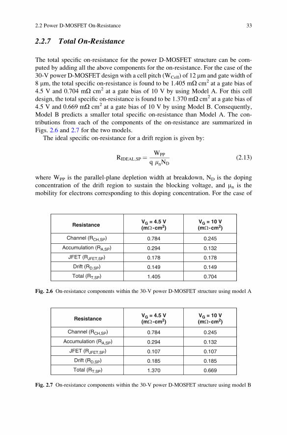
2.2.7 Total On-Resistance
The total specific on-resistance for the power D-MOSFET structure can be com-
puted by adding all the above components for the on-resistance. For the case of the
30-V power D-MOSFET design with a cell pitch (WCell) of 12 mm and gate width of
8 mm, the total specific on-resistance is found to be 1.405 mO cm2 at a gate bias of
4.5 V and 0.704 mO cm2 at a gate bias of 10 V by using Model A. For this cell
design, the total specific on-resistance is found to be 1.370 mO cm2 at a gate bias of
4.5 V and 0.669 mO cm2 at a gate bias of 10 V by using Model B. Consequently,
Model B predicts a smaller total specific on-resistance than Model A. The con-
tributions from each of the components of the on-resistance are summarized in
Figs. 2.6 and 2.7 for the two models.
The ideal specific on-resistance for a drift region is given by:
RIDEAL;SP ¼ WPP
q mnND
(2.13)
where WPP is the parallel-plane depletion width at breakdown, ND is the doping
concentration of the drift region to sustain the blocking voltage, and mn is the
mobility for electrons corresponding to this doping concentration. For the case of
Resistance VG = 4.5 V(mΩ -cm2)
Channel (RCH,SP)
Accumulation (RA,SP)
JFET (RJFET,SP)
Drift (RD,SP)
Total (RT,SP)
VG = 10 V(mΩ -cm2)
0.245
0.132
0.178
0.149
0.704
0.784
0.294
0.178
0.149
1.405
Fig. 2.6 On-resistance components within the 30-V power D-MOSFET structure using model A
ResistanceVG = 4.5 V(mΩ -cm2)
Channel (RCH,SP)
Accumulation (RA,SP)
JFET (RJFET,SP)
Drift (RD,SP)
Total (RT,SP)
VG = 10 V(mΩ-cm2)
0.245
0.132
0.107
0.185
0.669
0.784
0.294
0.107
0.185
1.370
Fig. 2.7 On-resistance components within the 30-V power D-MOSFET structure using model B
2.2 Power D-MOSFET On-Resistance 33

a blocking voltage of 30 V, the depletion width and doping concentration are found
to be 2.2 � 1016/cm3 and 1.4 mm, respectively. Using the electron mobility for this
doping level, the ideal specific on-resistance is found to be 0.034 mO cm2. Since the
device is constrained by the impact of an 80% reduction of breakdown voltage due
to the edge termination, it is worth computing the ideal specific on-resistance for
this case for comparison with the device. For the case of a blocking voltage of
37.5 V, the depletion width and doping concentration are found to be 1.6 � 1016/cm3
and 1.8 mm, respectively. Using the electron mobility for this doping level, the ideal
specific on-resistance is found to be 0.059 mO cm2. It can be observed that
the specific on-resistance for the D-MOSFET structure is far greater than these
ideal specific on-resistances.
2.2.7.1 Simulation Results
The results of two-dimensional numerical simulations on the 30-V power
D-MOSFET structure are described here to provide a more detailed understanding
of the underlying device physics and operation. The structure used for the numeri-
cal simulations had a drift region thickness of 2.6 mm below the P+ region with a
doping concentration of 1.6 � 1016/cm3. The P-base region and N+ source regions
had depths of 1.7 and 0.7 mm, respectively. The doping concentration in the JFET
region was enhanced by using an additional n-type doping concentration of
1 � 1016/cm3 with a depth of 1.5 mm. For the numerical simulations, half the cell
(with a width of 6 mm) shown in Fig. 2.1 was utilized as a unit cell that is
representative of the structure.
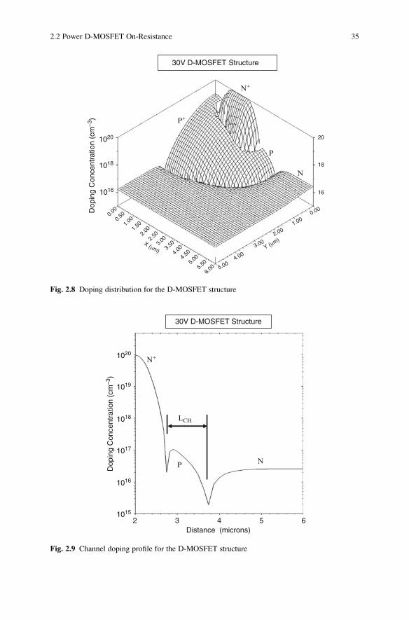
A three dimensional view of the doping distribution in the D-MOSFET structure
is shown in Fig. 2.8 from the left hand edge of the structure to the center of the
polysilicon gate region. The N+ source and P-base regions are aligned to the gate
edge, which is located at 2 mm from the left hand side. The structure also includes a
P+ region located at the left hand side to suppress the parasitic bipolar transistor.
The enhancement of the doping in the N-drift region near the surface is due to the
additional JFET doping.
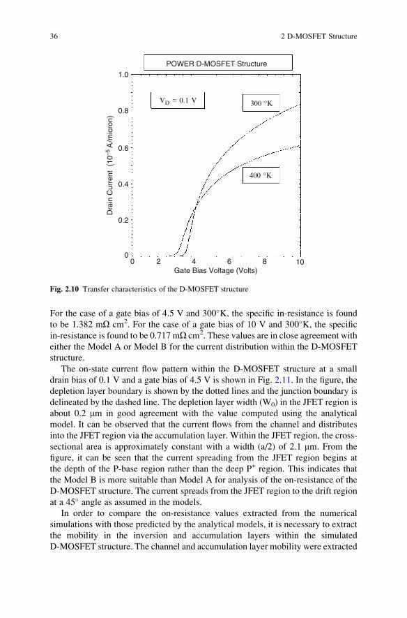
The lateral doping profile taken along the surface under the gate electrode is
shown in Fig. 2.9. From the profile, it can be observed that the doping concentration
of the JFET region has been increased to 2.3 � 1016/cm3 due to the additional
doping. The lateral extension of the P-base and N+ source regions are 1.7 and
0.7 mm leading to a channel length of 1.0 mm. The surface concentration for the
P-base region was chosen to obtain a maximum compensated P-type doping
concentration in the channel of 1.0 � 1017/cm3.
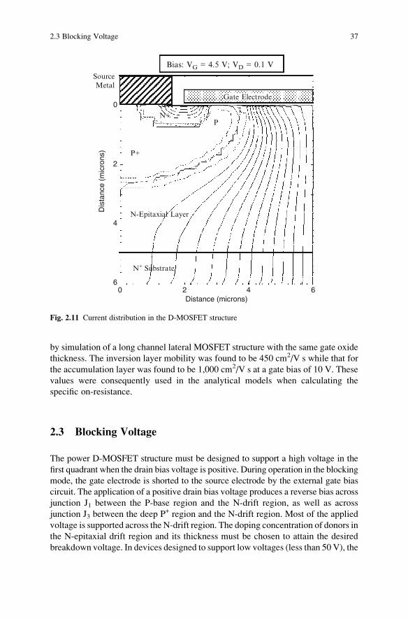
The transfer characteristics for the D-MOSFET structure were obtained using
numerical simulations with a drain bias of 0.1 V at 300 and 400�K. The resulting
transfer characteristics are shown in Fig. 2.10. From this graph, a threshold voltage
of 3.1 and 2.6 V can be extracted at 300 and 400�K, respectively. The threshold
voltage decreases by 16% when the temperature increases. The specific on-
resistance can be obtained from the transfer characteristics at any gate bias voltage.
34 2 D-MOSFET Structure
Dop
ing
Con
cent
ratio
n (c
m–3
)
30V D-MOSFET Structure
1016
1018
1020
N+
P+
P
N
20
18
16
0.00
0.50
1.00
1.50
2.00
2.50
3.00
3.50
4.00
4.50
5.00
5.50
6.00
Y (μm)X (μm)
5.004.00
3.00
2.001.00
0.00
Fig. 2.8 Doping distribution for the D-MOSFET structure
N+
P N
LCH
Dop
ing
Con
cent
ratio
n (c
m–3
)
30V D-MOSFET Structure
1016
1015
1017
1018
1019
1020
2 3 4 5 6Distance (microns)
Fig. 2.9 Channel doping profile for the D-MOSFET structure
2.2 Power D-MOSFET On-Resistance 35
For the case of a gate bias of 4.5 V and 300�K, the specific in-resistance is found
to be 1.382 mO cm2. For the case of a gate bias of 10 V and 300�K, the specific
in-resistance is found to be 0.717 mO cm2. These values are in close agreement with
either the Model A or Model B for the current distribution within the D-MOSFET
structure.
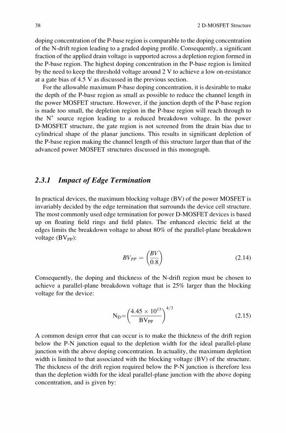
The on-state current flow pattern within the D-MOSFET structure at a small
drain bias of 0.1 V and a gate bias of 4.5 V is shown in Fig. 2.11. In the figure, the
depletion layer boundary is shown by the dotted lines and the junction boundary is
delineated by the dashed line. The depletion layer width (W0) in the JFET region is
about 0.2 mm in good agreement with the value computed using the analytical
model. It can be observed that the current flows from the channel and distributes
into the JFET region via the accumulation layer. Within the JFET region, the cross-
sectional area is approximately constant with a width (a/2) of 2.1 mm. From the
figure, it can be seen that the current spreading from the JFET region begins at
the depth of the P-base region rather than the deep P+ region. This indicates that
the Model B is more suitable than Model A for analysis of the on-resistance of the
D-MOSFET structure. The current spreads from the JFET region to the drift region
at a 45� angle as assumed in the models.
In order to compare the on-resistance values extracted from the numerical
simulations with those predicted by the analytical models, it is necessary to extract
the mobility in the inversion and accumulation layers within the simulated
D-MOSFET structure. The channel and accumulation layer mobility were extracted
POWER D-MOSFET Structure
00 2 4 6 8
Gate Bias Voltage (Volts)
0.8
1.0
0.6
0.4
0.2
VD = 0.1 V
400 °K
300 °K
10
Dra
in C
urre
nt (
10–5
A/m
icro
n)
Fig. 2.10 Transfer characteristics of the D-MOSFET structure
36 2 D-MOSFET Structure
by simulation of a long channel lateral MOSFET structure with the same gate oxide
thickness. The inversion layer mobility was found to be 450 cm2/V s while that for
the accumulation layer was found to be 1,000 cm2/V s at a gate bias of 10 V. These
values were consequently used in the analytical models when calculating the
specific on-resistance.
2.3 Blocking Voltage
The power D-MOSFET structure must be designed to support a high voltage in the
first quadrant when the drain bias voltage is positive. During operation in the blocking
mode, the gate electrode is shorted to the source electrode by the external gate bias
circuit. The application of a positive drain bias voltage produces a reverse bias across
junction J1 between the P-base region and the N-drift region, as well as across
junction J3 between the deep P+ region and the N-drift region. Most of the applied
voltage is supported across the N-drift region. The doping concentration of donors in
the N-epitaxial drift region and its thickness must be chosen to attain the desired
breakdown voltage. In devices designed to support low voltages (less than 50 V), the
N-Epitaxial Layer
N+
P+
P
Distance (microns)
0
2
4
6
Source Metal
Dis
tanc
e (m
icro
ns)
Bias: VG = 4.5 V; VD = 0.1 V
N+ Substrate
0 2 4 6
Gate Electrode
Fig. 2.11 Current distribution in the D-MOSFET structure
2.3 Blocking Voltage 37
doping concentration of the P-base region is comparable to the doping concentration
of the N-drift region leading to a graded doping profile. Consequently, a significant
fraction of the applied drain voltage is supported across a depletion region formed in
the P-base region. The highest doping concentration in the P-base region is limited
by the need to keep the threshold voltage around 2 V to achieve a low on-resistance
at a gate bias of 4.5 V as discussed in the previous section.
For the allowable maximum P-base doping concentration, it is desirable to make
the depth of the P-base region as small as possible to reduce the channel length in
the power MOSFET structure. However, if the junction depth of the P-base region
is made too small, the depletion region in the P-base region will reach through to
the N+ source region leading to a reduced breakdown voltage. In the power
D-MOSFET structure, the gate region is not screened from the drain bias due to
cylindrical shape of the planar junctions. This results in significant depletion of
the P-base region making the channel length of this structure larger than that of the
advanced power MOSFET structures discussed in this monograph.
2.3.1 Impact of Edge Termination
In practical devices, the maximum blocking voltage (BV) of the power MOSFET is
invariably decided by the edge termination that surrounds the device cell structure.
The most commonly used edge termination for power D-MOSFET devices is based
up on floating field rings and field plates. The enhanced electric field at the
edges limits the breakdown voltage to about 80% of the parallel-plane breakdown
voltage (BVPP):
BVPP ¼ BV
0:8
� �(2.14)
Consequently, the doping and thickness of the N-drift region must be chosen to
achieve a parallel-plane breakdown voltage that is 25% larger than the blocking
voltage for the device:
ND¼ 4:45� 1013
BVPP
� �4=3
(2.15)
A common design error that can occur is to make the thickness of the drift region
below the P-N junction equal to the depletion width for the ideal parallel-plane
junction with the above doping concentration. In actuality, the maximum depletion
width is limited to that associated with the blocking voltage (BV) of the structure.
The thickness of the drift region required below the P-N junction is therefore less
than the depletion width for the ideal parallel-plane junction with the above doping
concentration, and is given by:
38 2 D-MOSFET Structure
t ¼ WD BVð Þ ¼ffiffiffiffiffiffiffiffiffiffiffiffiffi2eSBVqND
s(2.16)
The resistance of the drift region can be reduced by using this thickness rather than the
maximum depletion width corresponding to the doping concentration given by (2.15).
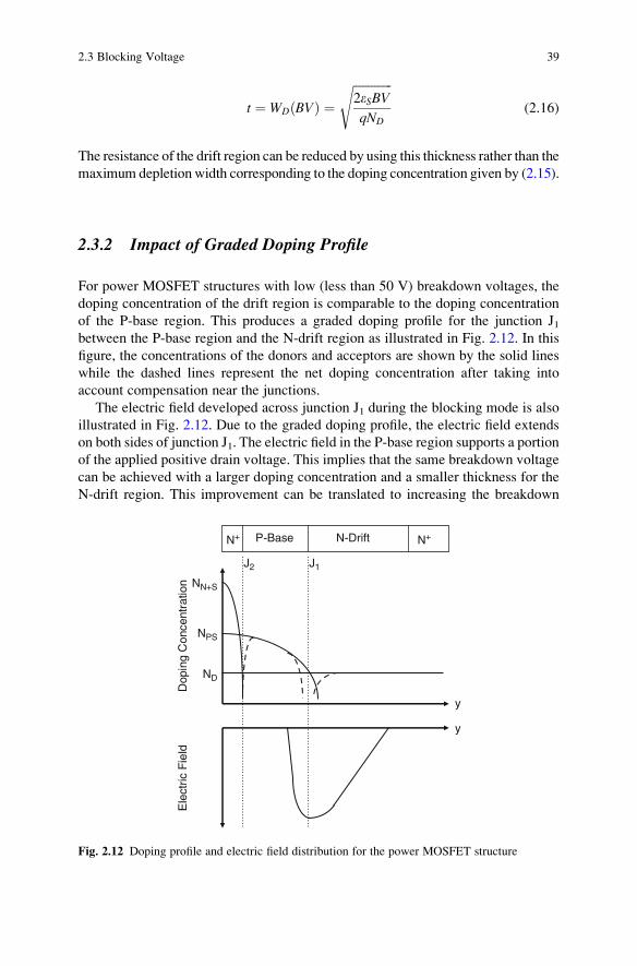
2.3.2 Impact of Graded Doping Profile
For power MOSFET structures with low (less than 50 V) breakdown voltages, the
doping concentration of the drift region is comparable to the doping concentration
of the P-base region. This produces a graded doping profile for the junction J1between the P-base region and the N-drift region as illustrated in Fig. 2.12. In this
figure, the concentrations of the donors and acceptors are shown by the solid lines
while the dashed lines represent the net doping concentration after taking into
account compensation near the junctions.
The electric field developed across junction J1 during the blocking mode is also
illustrated in Fig. 2.12. Due to the graded doping profile, the electric field extends
on both sides of junction J1. The electric field in the P-base region supports a portion
of the applied positive drain voltage. This implies that the same breakdown voltage
can be achieved with a larger doping concentration and a smaller thickness for the
N-drift region. This improvement can be translated to increasing the breakdown
N+ N+
Ele
ctric
Fie
ld
y
N-Drift
Dop
ing
Con
cent
ratio
n
y
ND
NPS
NN+S
P-Base
J1J2
Fig. 2.12 Doping profile and electric field distribution for the power MOSFET structure
2.3 Blocking Voltage 39
voltage at the edge termination if the P-base region is used at the edges of the power
MOSFET structure. A reduction of the resistance for the power MOSFET structure
can be achieved by taking into account the voltage supported within the P-base
region. An improvement in the specific on-resistance of 20% can be achieved by
taking into account the graded doping profile.
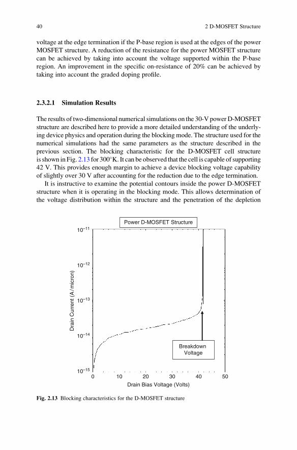
2.3.2.1 Simulation Results
The results of two-dimensional numerical simulations on the 30-V powerD-MOSFET
structure are described here to provide a more detailed understanding of the underly-
ing device physics and operation during the blocking mode. The structure used for the
numerical simulations had the same parameters as the structure described in the
previous section. The blocking characteristic for the D-MOSFET cell structure
is shown in Fig. 2.13 for 300�K. It can be observed that the cell is capable of supporting42 V. This provides enough margin to achieve a device blocking voltage capability
of slightly over 30 V after accounting for the reduction due to the edge termination.
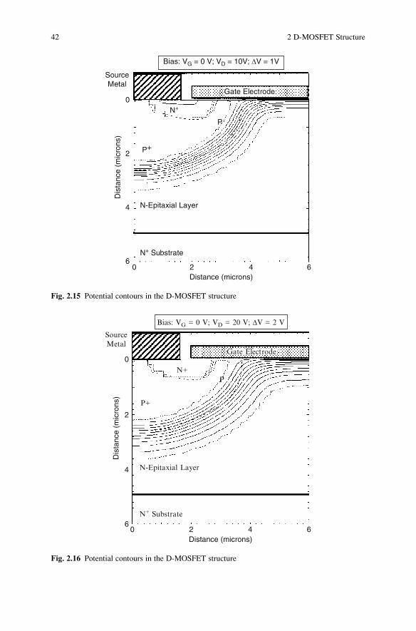
It is instructive to examine the potential contours inside the power D-MOSFET
structure when it is operating in the blocking mode. This allows determination of
the voltage distribution within the structure and the penetration of the depletion
Dra
in C
urre
nt (
A/m
icro
n)
Power D-MOSFET Structure
0
Drain Bias Voltage (Volts)
10–11
10–12
10–13
10–14
10–15
Breakdown Voltage
10 20 30 40 50
Fig. 2.13 Blocking characteristics for the D-MOSFET structure
40 2 D-MOSFET Structure

region in the P-base region with increasing drain bias voltage. The potential
contours for the D-MOSFET structure obtained using the numerical simulations
with zero gate bias and various drain bias voltages are shown in Figs. 2.14–2.17.
From these figures, it can be observed that the voltage distribution at the junction J1between the P-base region and the N-drift region is similar when proceeding from
the surface towards the drain. This indicates that the surface region is not screened
from the drain bias by the junctions. Consequently, the depletion region in the
P-base region penetrates through a significant fraction of the P-base region when
the drain bias is increased to 30 V. Any decrease in the doping concentration of the
P-base region leads to reach-through breakdown limiting the ability to reduce the
threshold voltage. The advanced power MOSFET structures discussed in
subsequent chapters allow the screening of the semiconductor surface under the
gate from the drain potential allowing the formation of shorter channel lengths to
reduce the on-resistance.
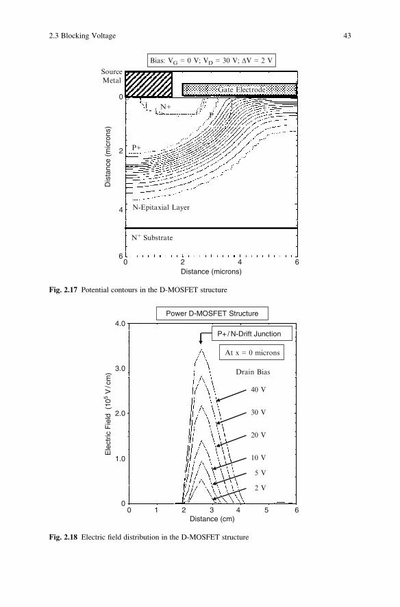
It is insightful to also examine the electric field profile inside the power
D-MOSFET structure when it is operating in the blocking mode. The electric
field profile obtained through the junction between the deep P+ region and
the N-drift region is shown in Fig. 2.18. It can be observed that the maximum
electric field occurs as expected at the junction at a depth of 2.6 mm from the
surface. This figure demonstrates that a substantial portion of the voltage is
supported inside the P+ region due to its graded doping profile near the junction.
N-Epitaxial Layer
N+
P+
P
0 2 4 6Distance (microns)
0
2
4
6N+ Substrate
SourceMetal
Dis
tanc
e (m
icro
ns)
Bias: VG = 0 V; VD = 5V; DV = 1V
Gate Electrode
Fig. 2.14 Potential contours in the D-MOSFET structure
2.3 Blocking Voltage 41
SourceMetal
N-Epitaxial Layer
N+
P+
P
0 2 4 6Distance (microns)
0
2
4
6N+ Substrate
Dis
tanc
e (m
icro
ns)
Bias: VG = 0 V; VD = 10V; ΔV = 1V
Gate Electrode
Fig. 2.15 Potential contours in the D-MOSFET structure
N-Epitaxial Layer
N+
P+
P
0 2 4 6Distance (microns)
0
2
4
6N+ Substrate
SourceMetal
Dis
tanc
e (m
icro
ns)
Bias: VG = 0 V; VD = 20 V; ΔV = 2 V
Gate Electrode
Fig. 2.16 Potential contours in the D-MOSFET structure
42 2 D-MOSFET Structure
N-Epitaxial Layer
N+
P+
P
0 2 4 6Distance (microns)
0
2
4
6
N+ Substrate
SourceMetal
Dis
tanc
e (m
icro
ns)
Bias: VG = 0 V; VD = 30 V; ΔV = 2 V
Gate Electrode
Fig. 2.17 Potential contours in the D-MOSFET structure
Ele
ctric
Fie
ld (
105
V/c
m)
0
3.0
4.0
2.0
1.0
Power D-MOSFET Structure
5 V
10 V
20 V
30 V
40 V
2 V
Drain Bias
P+ / N-Drift Junction
Distance (cm)
At x = 0 microns
0 2 41 3 5 6
Fig. 2.18 Electric field distribution in the D-MOSFET structure
2.3 Blocking Voltage 43
The doping concentration for the N-drift region can be increased while achieving
the target blocking voltage capability due to this phenomenon. This allows reduc-
tion of the specific on-resistance for the power D-MOSFET structure.
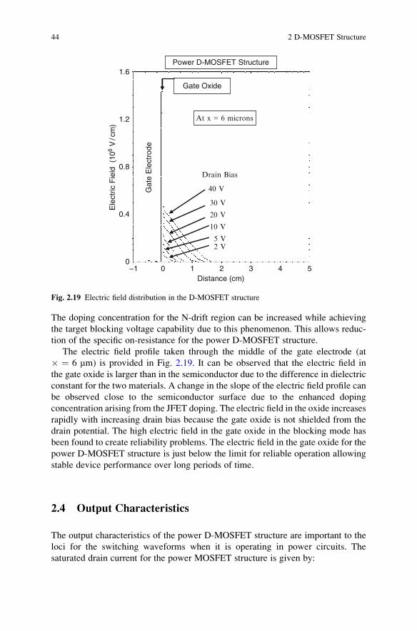
The electric field profile taken through the middle of the gate electrode (at
� ¼ 6 mm) is provided in Fig. 2.19. It can be observed that the electric field in
the gate oxide is larger than in the semiconductor due to the difference in dielectric
constant for the two materials. A change in the slope of the electric field profile can
be observed close to the semiconductor surface due to the enhanced doping
concentration arising from the JFET doping. The electric field in the oxide increases
rapidly with increasing drain bias because the gate oxide is not shielded from the
drain potential. The high electric field in the gate oxide in the blocking mode has
been found to create reliability problems. The electric field in the gate oxide for the
power D-MOSFET structure is just below the limit for reliable operation allowing
stable device performance over long periods of time.
2.4 Output Characteristics
The output characteristics of the power D-MOSFET structure are important to the
loci for the switching waveforms when it is operating in power circuits. The
saturated drain current for the power MOSFET structure is given by:
Ele
ctric
Fie
ld (
106
V/c
m)
00 2 4
Distance (cm)
1.2
1.6
0.8
0.4
1 3 5
Power D-MOSFET Structure
5 V
10 V
20 V
30 V
40 V
2 V
Drain Bias
Gate Oxide
Gat
e E
lect
rode
At x = 6 microns
–1
Fig. 2.19 Electric field distribution in the D-MOSFET structure
44 2 D-MOSFET Structure
ID;sat ¼ ZmniCOX
LCH � DLCHð Þ VG � VTHð Þ2 (2.17)
where DLCH is reduction in the channel length due to depletion of the P-base region
with increasing drain bias voltage. With sufficiently high doping concentration of
the P-base region, the modulation of channel length can be made sufficiently small
to ensure a high output resistance. The saturated drain current in the power
D-MOSFET structure then increases as the square of the gate bias voltage.
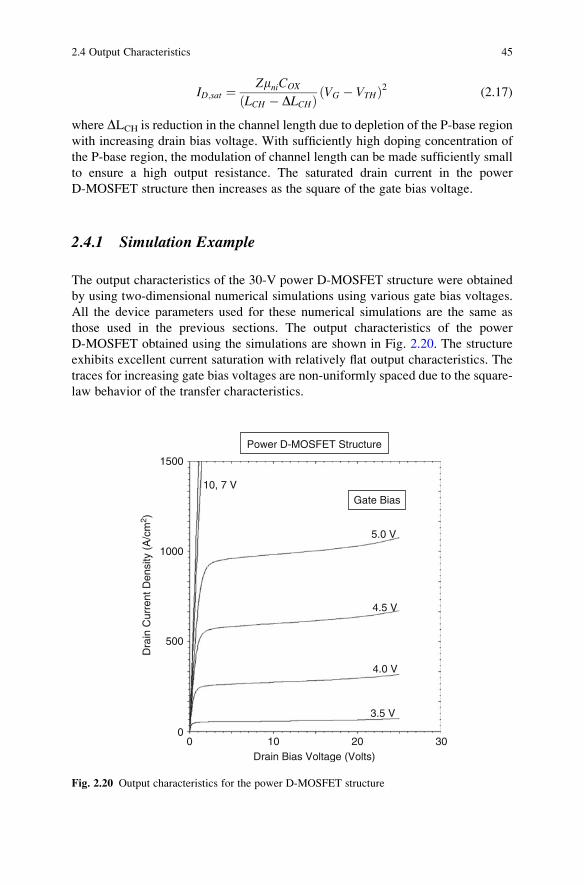
2.4.1 Simulation Example
The output characteristics of the 30-V power D-MOSFET structure were obtained
by using two-dimensional numerical simulations using various gate bias voltages.
All the device parameters used for these numerical simulations are the same as
those used in the previous sections. The output characteristics of the power
D-MOSFET obtained using the simulations are shown in Fig. 2.20. The structure
exhibits excellent current saturation with relatively flat output characteristics. The
traces for increasing gate bias voltages are non-uniformly spaced due to the square-
law behavior of the transfer characteristics.
Dra
in C
urre
nt D
ensi
ty (
A/c
m2 )
Power D-MOSFET Structure
0 10 20 30Drain Bias Voltage (Volts)
1500
1000
500
0
3.5 V
4.0 V
4.5 V
5.0 V
10, 7 VGate Bias
Fig. 2.20 Output characteristics for the power D-MOSFET structure
2.4 Output Characteristics 45
2.5 Device Capacitances
One of attractive features of all power MOSFET structures is unipolar current
transport. The absence of minority carrier injection allows interruption of the
current flow immediately after reduction of the gate bias below the threshold
voltage. Although this implies a very fast switching speed for the power MOSFET
structures, in practice the switching speed is limited by the device capacitances.
The input drive signal for a power MOSFET structure is applied to the gate
electrode, which is a part of a Metal-Oxide-Semiconductor sandwich. Due to
the small thickness of the gate oxide and large device active area, the MOS
sandwich comprises a significant capacitance. Analysis of this capacitance
requires taking into account the formation of a depletion layer in the semiconduc-
tor under certain bias conditions. The rate at which the power MOSFET structure
can be switched between the on- and off-states is determined by the rate at which
the input capacitance can be charged or discharged. In addition, the capacitance
between the drain and the gate electrodes has been found to play an important
role in determining the drain current and voltage transitions during the switching
event.
The capacitances within the power D-MOSFET structure have been analyzed in
detail in the textbook [1]. The specific input (or gate) capacitance for the power
D-MOSFET structure is given by:
CIN;SP ¼CNþ þCP þCSM ¼ 2xJP
WCell
eOXtOX
� �þ WG
WCell
eOXtIEOX
� �(2.18)
where tOX and tIEOX are the thicknesses of the gate and inter-electrode oxides,
respectively. For a 30-V power D-MOSFET structure with a cell pitch (WCELL in
Fig. 2.4) of 12 mm and gate electrode width of 8 mm, the input capacitance is found
to be 22 nF/cm2 for a gate oxide thickness of 500 A and an inter-metal dielectric
thickness of 5,000 A.
The capacitance between the gate and drain electrodes (also called the reverse
transfer capacitance) is determined by the width of the JFET region where the
gate electrode overlaps the N-drift region. The MOS structure in this portion of the
power D-MOSFET structure operates under deep depletion conditions when a
positive voltage is applied to the drain. The gate-drain capacitance for the power
D-MOSFET structure is given by:
CGD;SP ¼ WG � 2xPLð ÞWCell
COXCS;M
COX þ CS;M
� �(2.19)
where CS,M is the semiconductor capacitance under the gate oxide, which decreases
with increasing drain bias voltage. The specific capacitance of the semiconductor
depletion region can be obtained by computation of the depletion layer width.
46 2 D-MOSFET Structure
The depletion layer width in the semiconductor under the gate oxide can be
obtained using:
WD;MOS ¼ eSCOX
ffiffiffiffiffiffiffiffiffiffiffiffiffiffiffiffiffiffiffiffiffiffiffiffiffi1þ 2VDC2
OX
qeSND
s� 1
8<:
9=; (2.20)
The specific capacitance for the semiconductor is then obtained using:
CS;M ¼ eSWD;MOS
(2.21)
The gate-drain (or reverse transfer) capacitance can be computed by using (2.19)
with the above equations to determine the semiconductor capacitance as a function
of the drain bias voltage.
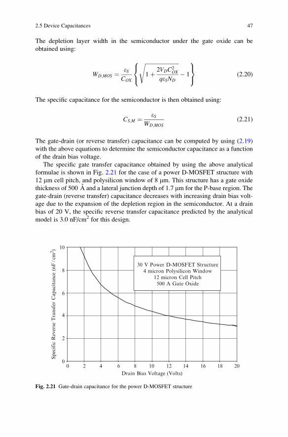
The specific gate transfer capacitance obtained by using the above analytical
formulae is shown in Fig. 2.21 for the case of a power D-MOSFET structure with
12 mm cell pitch, and polysilicon window of 8 mm. This structure has a gate oxide
thickness of 500 A and a lateral junction depth of 1.7 mm for the P-base region. The
gate-drain (reverse transfer) capacitance decreases with increasing drain bias volt-
age due to the expansion of the depletion region in the semiconductor. At a drain
bias of 20 V, the specific reverse transfer capacitance predicted by the analytical
model is 3.0 nF/cm2 for this design.
64 12108Drain Bias Voltage (Volts)
0
4
10
6
830 V Power D-MOSFET Structure
4 micron Polysilicon Window12 micron Cell Pitch500 A Gate Oxide
2
2 201816140
Spec
ific
Rev
erse
Tra
nsfe
r C
apac
itan
ce (
nF/c
m2 )
Fig. 2.21 Gate-drain capacitance for the power D-MOSFET structure
2.5 Device Capacitances 47
The output capacitance for the power D-MOSFET structure is associated with
the capacitance of the junction between the P-base region and the N-drift region.
The specific junction capacitance is given by [1]:
CS;J ¼ eSWD;J
(2.22)
where the depletion region thickness at the junction (WD,J) is related to the drain
bias voltage:
WD;J ¼ffiffiffiffiffiffiffiffiffiffiffiffiffiffiffiffiffiffiffiffiffiffiffiffiffiffiffiffi2eS VD þ Vbið Þ
qND
s(2.23)
This depletion layer width is larger than that under the gate oxide because all the
applied drain voltage must be supported across the P-N junction. The specific
output capacitance for the power D-MOSFET structure can then be obtained by
assuming (Model A in the textbook) that the area of the junction within the cell is
(WPW + 2xPL)Z:
CO ¼ WPW þ 2xPLWCell
� �CS;J (2.24)
where xPL is the lateral extension of the P-base region under the gate electrode.
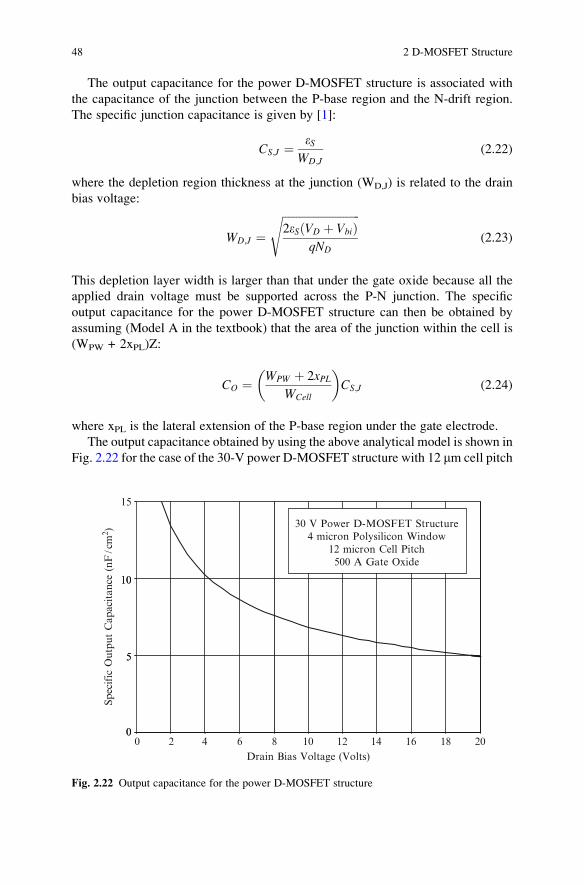
The output capacitance obtained by using the above analytical model is shown in
Fig. 2.22 for the case of the 30-V power D-MOSFET structure with 12 mm cell pitch
Spec
ific
Out
put C
apac
itan
ce (nF
/cm
2 )
0
5
10
20181614121080Drain Bias Voltage (Volts)
0
5
15
10
30 V Power D-MOSFET Structure4 micron Polysilicon Window
12 micron Cell Pitch500 A Gate Oxide
642
Fig. 2.22 Output capacitance for the power D-MOSFET structure
48 2 D-MOSFET Structure
and polysilicon window of 8 mm. This structure has a gate oxide thickness of 500 A
and a lateral junction depth of 1.7 mm for the P-base region. A built-in potential of
0.8 V was assumed for the P-base/N-drift junction, and the drift region has a doping
concentration of 1.6 � 1016/cm3. The specific output capacitance decreases with
increasing drain bias voltage due to the expansion of the depletion region under the
P-base region. At a drain bias of 20 V, the specific output capacitance predicted by
the analytical model for this structure is 5 nF/cm2.
2.5.1 Simulation Example
The capacitances of the 30-V power D-MOSFET structure were extracted using
two-dimensional numerical simulations on the structure with device parameters
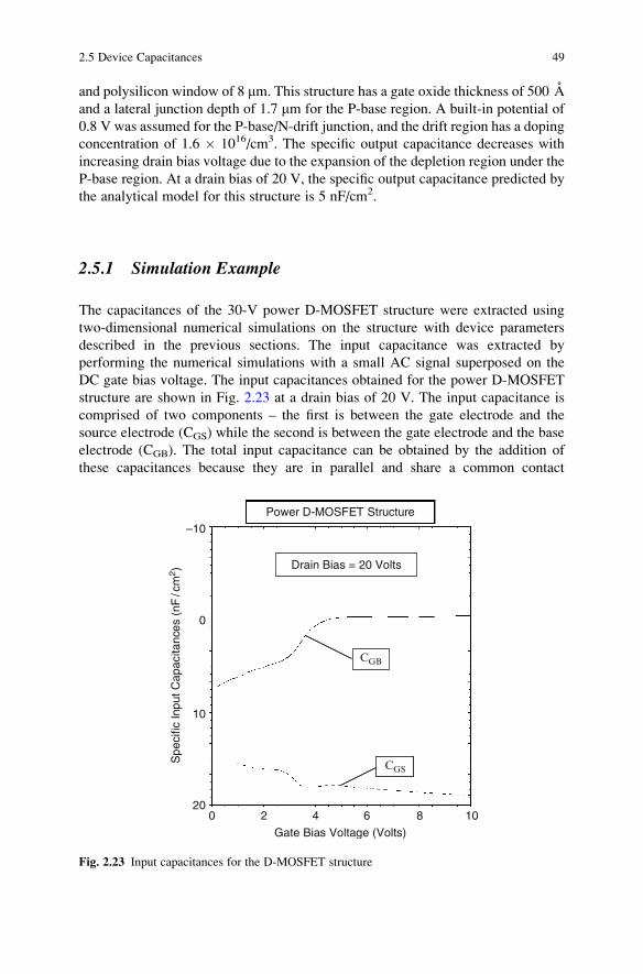
described in the previous sections. The input capacitance was extracted by
performing the numerical simulations with a small AC signal superposed on the
DC gate bias voltage. The input capacitances obtained for the power D-MOSFET
structure are shown in Fig. 2.23 at a drain bias of 20 V. The input capacitance is
comprised of two components – the first is between the gate electrode and the
source electrode (CGS) while the second is between the gate electrode and the base
electrode (CGB). The total input capacitance can be obtained by the addition of
these capacitances because they are in parallel and share a common contact
Power D-MOSFET Structure
200 2 4 6 8 10
0
–10
10
Drain Bias = 20 Volts
Spe
cific
Inpu
t Cap
acita
nces
(nF
/cm
2 )
Gate Bias Voltage (Volts)
CGS
CGB
Fig. 2.23 Input capacitances for the D-MOSFET structure
2.5 Device Capacitances 49
electrode in the actual power D-MOSFET structure. From the figure, a total specific
input capacitance of about 20 nF/cm2 is observed which is approximately indepen-
dent of the gate bias voltage. At gate bias voltages below the threshold voltage,
there is significant coupling between the P-base region and the gate electrode
leading to a large contribution to the input capacitance from this path. When the
gate bias voltage exceeds the threshold voltage, the inversion layer screens the
P-base region from the gate electrode and couples it with the N+ source region.
Consequently, the contribution from CGB decreases to zero while that from CGS
increases as the gate bias voltage is increased. The specific input capacitance
extracted from the numerical simulations is in excellent agreement with that
calculated with the analytical model.
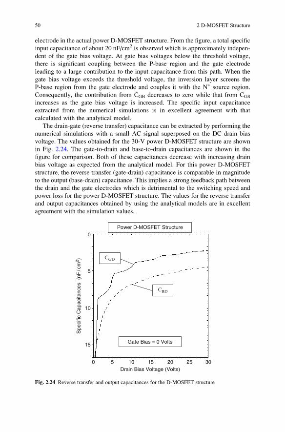
The drain-gate (reverse transfer) capacitance can be extracted by performing the
numerical simulations with a small AC signal superposed on the DC drain bias
voltage. The values obtained for the 30-V power D-MOSFET structure are shown
in Fig. 2.24. The gate-to-drain and base-to-drain capacitances are shown in the
figure for comparison. Both of these capacitances decrease with increasing drain
bias voltage as expected from the analytical model. For this power D-MOSFET
structure, the reverse transfer (gate-drain) capacitance is comparable in magnitude
to the output (base-drain) capacitance. This implies a strong feedback path between
the drain and the gate electrodes which is detrimental to the switching speed and
power loss for the power D-MOSFET structure. The values for the reverse transfer
and output capacitances obtained by using the analytical models are in excellent
agreement with the simulation values.
Spe
cific
Cap
acita
nces
(nF
/cm
2 )
15
0 5 15 20 25 30Drain Bias Voltage (Volts)
0
10
CBD
Gate Bias = 0 Volts
10
5
Power D-MOSFET Structure
CGD
Fig. 2.24 Reverse transfer and output capacitances for the D-MOSFET structure
50 2 D-MOSFET Structure
2.6 Gate Charge
It is standard practice in the industry to provide the gate charge for power MOSFET
structures as a measure of their switching performance. The gate charge can be
extracted by the application of a constant current source at the gate terminal while
turning-on the power MOSFET structure from the blocking state. The linearized
current and voltage waveforms observed during the turn-on process are illustrated
in Fig. 6.98 in the textbook [1]. The various components for the gate charge are also
defined in this figure. During the turn-on process, the gate current is used to charge
the capacitances CGS and CGD shown in Fig. 6.97. The most significant gate charge
components for assessing the performance of the power MOSFET structures are
QSW (the gate switching charge), QGD (the gate-drain charge), and QG (the total
gate charge). These components are given by [1]:
QGD ¼ 2KGqeSND
COX
ffiffiffiffiffiffiffiffiffiffiffiffiffiffiffiffiffiffiffiffiffiffiffiffiffiffiffiffi1þ 2VDSC
2OX
qeSND
s�
ffiffiffiffiffiffiffiffiffiffiffiffiffiffiffiffiffiffiffiffiffiffiffiffiffiffiffiffi1þ 2VONC
2OX
qeSND
s24
35 (2.25)
QSW ¼ CGS þ CGD VDSð Þ½ �ffiffiffiffiffiffiffiffiffiffiffiffiffiffiffiffiffiffiffiffiffiffiffiffiffiffiJONWCellLCH
2mniCOX
s
þ 2KGqeSND
COX
ffiffiffiffiffiffiffiffiffiffiffiffiffiffiffiffiffiffiffiffiffiffiffiffiffiffiffiffi1þ 2VDSC
2OX
qeSND
s�
ffiffiffiffiffiffiffiffiffiffiffiffiffiffiffiffiffiffiffiffiffiffiffiffiffiffiffiffi1þ 2VONC
2OX
qeSND
s24
35 ð2:26Þ
QG ¼ CGS þ CGD VDSð Þ½ �VGP
þ 2KGqeSND
COX
ffiffiffiffiffiffiffiffiffiffiffiffiffiffiffiffiffiffiffiffiffiffiffiffiffiffiffiffi1þ 2VDSC
2OX
qeSND
s�
ffiffiffiffiffiffiffiffiffiffiffiffiffiffiffiffiffiffiffiffiffiffiffiffiffiffiffiffi1þ 2VONC
2OX
qeSND
s24
35
þ CGS þ CGD VONð Þ½ � VG�VGPð Þ
(2.27)
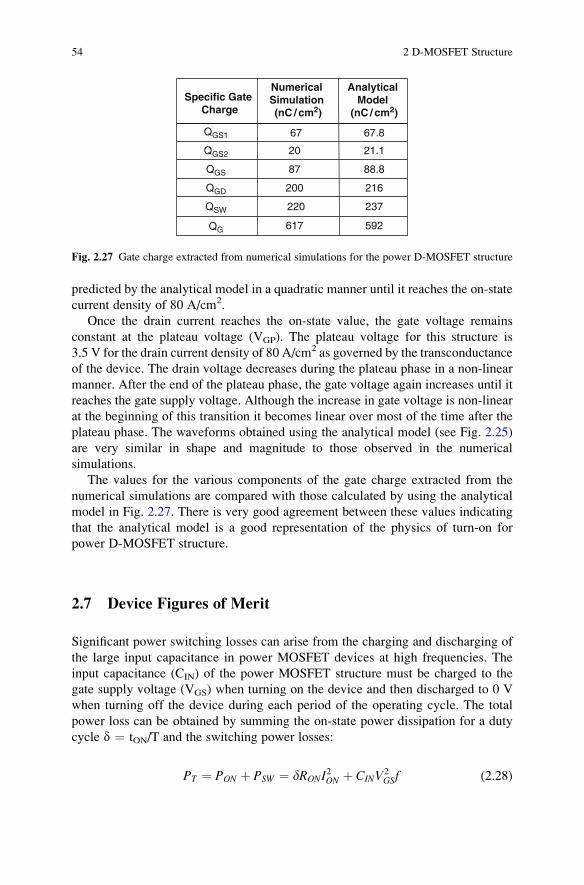
The gate charge values obtained for the 30-V power D-MOSFET structure by
using the above equations are: QGD ¼ 216 nC/cm2; QSW ¼ 237 nC/cm2; and
QG ¼ 592 nC/cm2. It can be concluded that the gate-drain charge (QGD) is the
dominant portion (90%) of the gate switching charge (QSW).
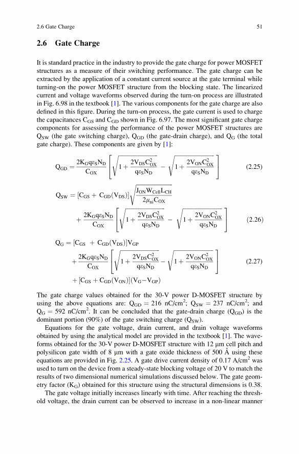
Equations for the gate voltage, drain current, and drain voltage waveforms
obtained by using the analytical model are provided in the textbook [1]. The wave-
forms obtained for the 30-V power D-MOSFET structure with 12 mm cell pitch and
polysilicon gate width of 8 mm with a gate oxide thickness of 500 A using these
equations are provided in Fig. 2.25. A gate drive current density of 0.17 A/cm2 was
used to turn on the device from a steady-state blocking voltage of 20 V to match the
results of two dimensional numerical simulations discussed below. The gate geom-
etry factor (KG) obtained for this structure using the structural dimensions is 0.38.
The gate voltage initially increases linearly with time. After reaching the thresh-
old voltage, the drain current can be observed to increase in a non-linear manner
2.6 Gate Charge 51
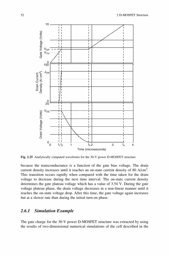
because the transconductance is a function of the gate bias voltage. The drain
current density increases until it reaches an on-state current density of 80 A/cm2.
This transition occurs rapidly when compared with the time taken for the drain
voltage to decrease during the next time interval. The on-state current density
determines the gate plateau voltage which has a value of 3.54 V. During the gate
voltage plateau phase, the drain voltage decreases in a non-linear manner until it
reaches the on-state voltage drop. After this time, the gate voltage again increases
but at a slower rate than during the initial turn-on phase.
2.6.1 Simulation Example
The gate charge for the 30-V power D-MOSFET structure was extracted by using
the results of two-dimensional numerical simulations of the cell described in the
Gat
e V
olta
ge (
Vol
ts)
10
0
Dra
in C
urre
ntD
ensi
ty (
A/c
m2 )
100
0
Dra
in V
olta
ge (
Vol
ts)
25
Time (microseconds)
0 1 2 3 40
t1 t2 t3 t4
VGPVTH
JON
VDS
Fig. 2.25 Analytically computed waveforms for the 30-V power D-MOSFET structure
52 2 D-MOSFET Structure
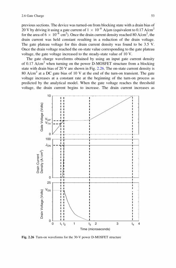
previous sections. The device was turned-on from blocking state with a drain bias of
20 V by driving it using a gate current of 1 � 10–8 A/mm (equivalent to 0.17 A/cm2
for the area of 6 � 10–8 cm2). Once the drain current density reached 80 A/cm2, the
drain current was held constant resulting in a reduction of the drain voltage.
The gate plateau voltage for this drain current density was found to be 3.5 V.
Once the drain voltage reached the on-state value corresponding to the gate plateau
voltage, the gate voltage increased to the steady-state value of 10 V.
The gate charge waveforms obtained by using an input gate current density
of 0.17 A/cm2 when turning on the power D-MOSFET structure from a blocking
state with drain bias of 20 V are shown in Fig. 2.26. The on-state current density is
80 A/cm2 at a DC gate bias of 10 V at the end of the turn-on transient. The gate
voltage increases at a constant rate at the beginning of the turn-on process as
predicted by the analytical model. When the gate voltage reaches the threshold
voltage, the drain current begins to increase. The drain current increases as
Gat
e V
olta
ge (
Vol
ts)
Dra
in C
urre
ntD
ensi
ty (
A/c
m2 )
D
rain
Vol
tage
(V
olts
)
Time (microseconds)
0 1 2 3 4t1 t2 t3 t4
10
0
100
25
0
VGPVTH
0
JON
VDS
Fig. 2.26 Turn-on waveforms for the 30-V power D-MOSFET structure
2.6 Gate Charge 53
predicted by the analytical model in a quadratic manner until it reaches the on-state
current density of 80 A/cm2.
Once the drain current reaches the on-state value, the gate voltage remains
constant at the plateau voltage (VGP). The plateau voltage for this structure is
3.5 V for the drain current density of 80 A/cm2 as governed by the transconductance
of the device. The drain voltage decreases during the plateau phase in a non-linear
manner. After the end of the plateau phase, the gate voltage again increases until it
reaches the gate supply voltage. Although the increase in gate voltage is non-linear
at the beginning of this transition it becomes linear over most of the time after the
plateau phase. The waveforms obtained using the analytical model (see Fig. 2.25)
are very similar in shape and magnitude to those observed in the numerical
simulations.
The values for the various components of the gate charge extracted from the
numerical simulations are compared with those calculated by using the analytical
model in Fig. 2.27. There is very good agreement between these values indicating
that the analytical model is a good representation of the physics of turn-on for
power D-MOSFET structure.
2.7 Device Figures of Merit
Significant power switching losses can arise from the charging and discharging of
the large input capacitance in power MOSFET devices at high frequencies. The
input capacitance (CIN) of the power MOSFET structure must be charged to the
gate supply voltage (VGS) when turning on the device and then discharged to 0 V
when turning off the device during each period of the operating cycle. The total
power loss can be obtained by summing the on-state power dissipation for a duty
cycle d ¼ tON/T and the switching power losses:
PT ¼ PON þ PSW ¼ dRONI2ON þ CINV
2GSf (2.28)
Specific Gate Charge
Numerical Simulation (nC / cm2)
Analytical Model
(nC / cm2)
QGS1 67 67.8
QGS2
QGS
QGD
QSW
QG
20 21.1
87 88.8
200 216
220 237
617 592
Fig. 2.27 Gate charge extracted from numerical simulations for the power D-MOSFET structure
54 2 D-MOSFET Structure

where RON is the on-resistance of the power MOSFET structure, ION is the on-state
current, and f is the operating frequency. In writing this equation, the switching
power losses due to the drain current and voltage transitions has been neglected. A
minimum total power loss occurs for each power MOSFET structure at an optimum
active area as shown in the textbook [1]. The on-state and switching power losses
are equal at the optimum active area. The optimum active area at which the power
dissipation is minimized is given by:
AOPT ¼ffiffiffiffiffiffiffiffiffiffiffiffiRON;sp
CIN;sp
sIONVGS
� � ffiffiffidf
s !(2.29)
From the first term in this expression, a useful technology figure-of-merit can be
defined:
FOMðAÞ ¼ RON;sp
CIN;sp(2.30)
In the power electronics community, there is trend towards increasing the operating
frequency for switch mode power supplies in order to reduce the size and weight of
the magnetic components. The ability to migrate to higher operating frequencies in
power conversion circuits is dependent on making enhancements to the power
MOSFET technology. From the above equations, an expression for the minimum
total power dissipation can be obtained [1]:
PT minð Þ ¼ 2IONVGS
ffiffiffiffiffiffiffiffiffiffiffiffiffiffiffiffiffiffiffiffiffiffiffiffiffiffiffiffidRON;spCIN;spf
p(2.31)
A second technology figure of merit related to the minimum power dissipation can
be defined as:
FOMðBÞ ¼ RON;spCIN;sp (2.32)
In most applications for power MOSFET structures with high operating frequency,
the switching losses associated with the drain current and voltage transitions
become a dominant portion of the total power loss. The time period associated
with the increase of the drain current and decrease of the drain voltage is deter-
mined by the charging of the device capacitances. It is therefore common practice
in the industry to use the following figures-of-merit to compare the performance of
power MOSFET products [1]:
FOMðCÞ ¼ RON;spQGD;sp (2.33)
and
FOMðDÞ ¼ RON;spQSW;sp (2.34)
2.7 Device Figures of Merit 55
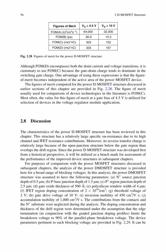
Although FOM(D) encompasses both the drain current and voltage transitions, it is
customary to use FOM(C) because the gate-drain charge tends to dominate in the
switching gate charge. One advantage of using these expressions is that the figure-
of-merit becomes independent of the active area of the power MOSFET device.
The figures of merit computed for the power D-MOSFET structure discussed in
earlier sections of this chapter are provided in Fig. 2.28. The figure of merit
usually used for comparison of device technologies in the literature is FOM(C).
Most often, the value for this figure of merit at a gate bias of 4.5 V is utilized for
selection of devices in the voltage regulator module application.
2.8 Discussion
The characteristics of the power D-MOSFET structure has been reviewed in this
chapter. This structure has a relatively large specific on-resistance due to its high
channel and JFET resistance contributions. Moreover, its reverse transfer charge is
relatively large because of the open-junction structure below the gate region than
overlaps the drift region. Since the power D-MOSFET structure was developed first
from a historical perspective, it will be utilized as a bench mark for assessment of
the performance of the improved device structures in subsequent chapters.
For purposes of comparison with the power MOSFET structures discussed in
subsequent chapters, the analysis of the power DMOSFET structure is provided
here for a broad range of blocking voltages. In this analysis, the power DMOSFET
structure was assumed to have the following parameters: (a) N+ source junction
depth of 0.5 mm; (b) P-base junction depth of 1.5 mm; (c) P+ region junction depth of
2.5 mm; (d) gate oxide thickness of 500 A; (e) polysilicon window width of 4 mm;
(f) JFET region doping concentration of 2 � 1016/cm3; (g) threshold voltage of
2 V; (h) gate drive voltage of 10 V; (i) inversion mobility of 450 cm2/V s; ( j)
accumulation mobility of 1,000 cm2/V s. The contributions from the contacts and
the N+ substrate were neglected during the analysis. The doping concentration and
thickness of the drift region were determined under the assumption that the edge
termination (in conjunction with the graded junction doping profiles) limits the
breakdown voltage to 90% of the parallel-plane breakdown voltage. The device
parameters pertinent to each blocking voltage are provided in Fig. 2.29. It can be
Figures of Merit VG = 4.5 V VG = 10 V
FOM(A) (Ω2cm4s–1)
FOM(C) (mΩ*nC)
FOM(D) (mΩ*nC)
64,000 32,000
FOM(B) (ps) 30.9 15.5
303 152
333 167
Fig. 2.28 Figures of merit for the power D-MOSFET structure
56 2 D-MOSFET Structure
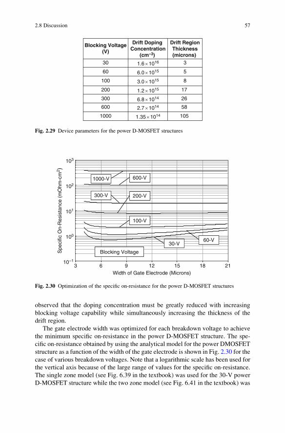
observed that the doping concentration must be greatly reduced with increasing
blocking voltage capability while simultaneously increasing the thickness of the
drift region.
The gate electrode width was optimized for each breakdown voltage to achieve
the minimum specific on-resistance in the power D-MOSFET structure. The spe-
cific on-resistance obtained by using the analytical model for the power DMOSFET
structure as a function of the width of the gate electrode is shown in Fig. 2.30 for the
case of various breakdown voltages. Note that a logarithmic scale has been used for
the vertical axis because of the large range of values for the specific on-resistance.
The single zone model (see Fig. 6.39 in the textbook) was used for the 30-V power
D-MOSFET structure while the two zone model (see Fig. 6.41 in the textbook) was
Blocking Voltage(V)
Drift Doping Concentration
(cm–3)
Drift RegionThickness(microns)
3
5
8
17
26
58
30 1.6 × 10¹⁶
60 6.0 × 10¹⁵
100 3.0 × 10¹⁵
200 1.2 × 10¹⁵
300 6.8 × 10¹⁴
600 2.7 × 10¹⁴
1000 1.35 × 10¹⁴ 105
Fig. 2.29 Device parameters for the power D-MOSFET structures
Spe
cific
On-
Res
ista
nce
(mO
hm-c
m2 )
Width of Gate Electrode (Microns)
10–1153 6 9 12 18 21
Blocking Voltage
100
101
102
103
30-V60-V
100-V
200-V
600-V
300-V
1000-V
Fig. 2.30 Optimization of the specific on-resistance for the power D-MOSFET structures
2.8 Discussion 57
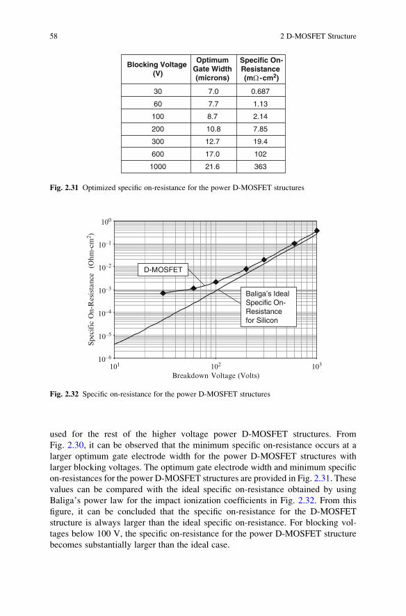
used for the rest of the higher voltage power D-MOSFET structures. From
Fig. 2.30, it can be observed that the minimum specific on-resistance occurs at a
larger optimum gate electrode width for the power D-MOSFET structures with
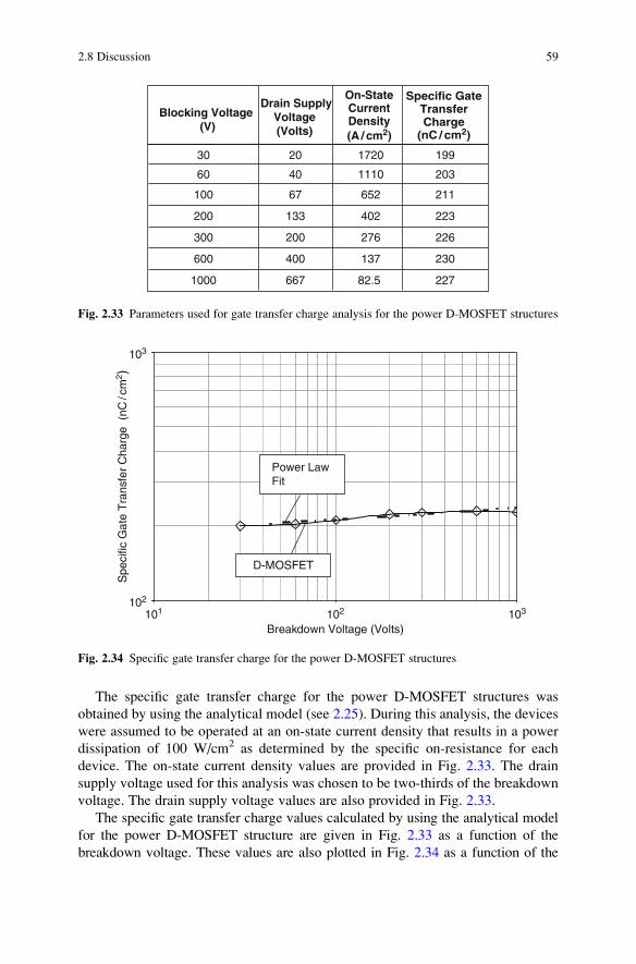
larger blocking voltages. The optimum gate electrode width and minimum specific
on-resistances for the power D-MOSFET structures are provided in Fig. 2.31. These
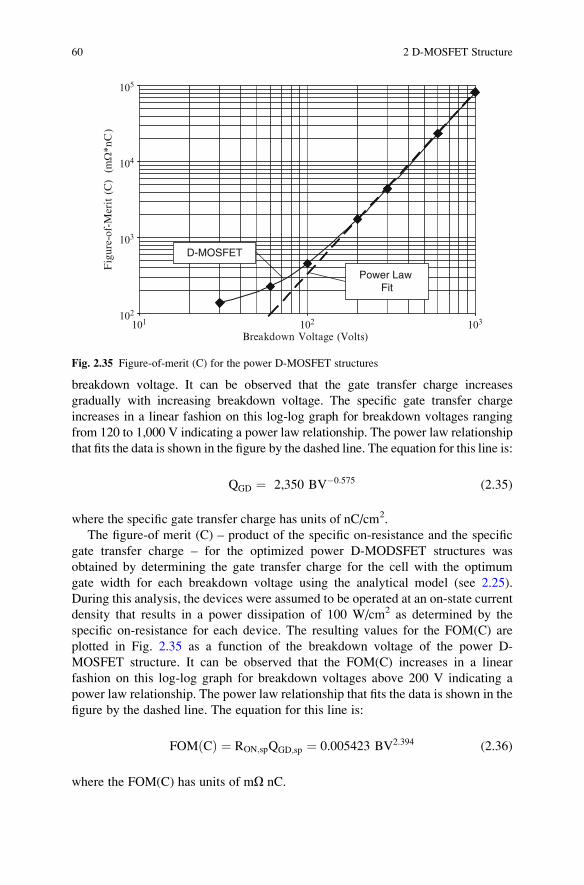
values can be compared with the ideal specific on-resistance obtained by using
Baliga’s power law for the impact ionization coefficients in Fig. 2.32. From this
figure, it can be concluded that the specific on-resistance for the D-MOSFET
structure is always larger than the ideal specific on-resistance. For blocking vol-
tages below 100 V, the specific on-resistance for the power D-MOSFET structure
becomes substantially larger than the ideal case.
Blocking Voltage (V)
Optimum Gate Width (microns)
Specific On-Resistance (mΩ-cm2)
30 7.0 0.687
60 7.7 1.13
100 8.7 2.14
200 10.8 7.85
300 12.7 19.4
600 17.0 102
1000 21.6 363
Fig. 2.31 Optimized specific on-resistance for the power D-MOSFET structures
10–6
10–5
10–4
10–3
10–2
10–1
100
Spec
ific
On-
Res
ista
nce
(O
hm-c
m2 )
Breakdown Voltage (Volts)101 102 103
D-MOSFET
Baliga’s Ideal Specific On-Resistance for Silicon
Fig. 2.32 Specific on-resistance for the power D-MOSFET structures
58 2 D-MOSFET Structure
The specific gate transfer charge for the power D-MOSFET structures was
obtained by using the analytical model (see 2.25). During this analysis, the devices
were assumed to be operated at an on-state current density that results in a power
dissipation of 100 W/cm2 as determined by the specific on-resistance for each
device. The on-state current density values are provided in Fig. 2.33. The drain
supply voltage used for this analysis was chosen to be two-thirds of the breakdown
voltage. The drain supply voltage values are also provided in Fig. 2.33.
The specific gate transfer charge values calculated by using the analytical model
for the power D-MOSFET structure are given in Fig. 2.33 as a function of the
breakdown voltage. These values are also plotted in Fig. 2.34 as a function of the
Blocking Voltage (V)
Drain SupplyVoltage (Volts)
On-State Current Density
Specific Gate Transfer Charge
(nC / cm2)
30 20 1720 199
60 40 1110 203
100 67 652 211
200 133 402 223
300 200 276 226
600 400 137 230
1000 667 82.5 227
(A / cm2)
Fig. 2.33 Parameters used for gate transfer charge analysis for the power D-MOSFET structures
Spe
cific
Gat
e T
rans
fer
Cha
rge
(nC
/cm
2 )
Breakdown Voltage (Volts)
D-MOSFET
Power Law Fit
101102
103
102 103
Fig. 2.34 Specific gate transfer charge for the power D-MOSFET structures
2.8 Discussion 59
breakdown voltage. It can be observed that the gate transfer charge increases
gradually with increasing breakdown voltage. The specific gate transfer charge
increases in a linear fashion on this log-log graph for breakdown voltages ranging
from 120 to 1,000 V indicating a power law relationship. The power law relationship
that fits the data is shown in the figure by the dashed line. The equation for this line is:
QGD ¼ 2,350 BV�0:575 (2.35)
where the specific gate transfer charge has units of nC/cm2.
The figure-of merit (C) – product of the specific on-resistance and the specific
gate transfer charge – for the optimized power D-MODSFET structures was
obtained by determining the gate transfer charge for the cell with the optimum
gate width for each breakdown voltage using the analytical model (see 2.25).
During this analysis, the devices were assumed to be operated at an on-state current
density that results in a power dissipation of 100 W/cm2 as determined by the
specific on-resistance for each device. The resulting values for the FOM(C) are
plotted in Fig. 2.35 as a function of the breakdown voltage of the power D-
MOSFET structure. It can be observed that the FOM(C) increases in a linear
fashion on this log-log graph for breakdown voltages above 200 V indicating a
power law relationship. The power law relationship that fits the data is shown in the
figure by the dashed line. The equation for this line is:
FOM Cð Þ ¼ RON;spQGD;sp ¼ 0.005423 BV2:394 (2.36)
where the FOM(C) has units of mO nC.
Fig
ure-
of-M
erit (C
) (
mΩ
*nC
)
Breakdown Voltage (Volts)
D-MOSFET
Power Law Fit
101102
103
104
105
102 103
Fig. 2.35 Figure-of-merit (C) for the power D-MOSFET structures
60 2 D-MOSFET Structure

The values for the specific on-resistance, and FOM(C) provided here for the power
D-MOSFET structure are useful as a benchmark to assess the performance of the
powerMOSFET structures that are discussed in subsequent chapters. Since the power
D-MOSFET technologywas developed in the 1970s, the manufacturing capability for
these devices is mature leading to low device costs. Any advanced power MOSFET
devices must provide substantial improvements in the specific on-resistance and
FOM(C) in order to displace the power D-MOSFET structures in applications.
References
1. B.J. Baliga, “Fundamentals of Power Semiconductor Devices”, Springer-Science, New York,
2008.
2. S.C. Sun and J.D. Plummer, “Modeling of the On-Resistance of LDMOS, VDMOS, and
VMOS Power Transistors”, IEEE Transactions on Electron Devices, Vol. ED-27,
pp. 356–367, 1980.
References 61

http://www.springer.com/978-1-4419-5916-4