Embed Size (px)
Citation preview

Chapter 2 A Simple, Clean-Metal Contact Resistance Model
A contact resistance model is presented in this chapter. The model assumes that the
contact surfaces are clean, that is, there are no insulating films at the contact interface.
The model also assumes that adhesion forces between the contact surfaces are negligible.
I first discuss the two broad components of the model - determining the distribution and
sizes of the areas in contact at the contact interface, as a function of the contact force; and
determining the contact resistance as a function of the distribution and sizes of the areas
in contact. Following a description of the model, the predicted contact force – contact
resistance characteristics are compared with the measured characteristics of a
microswitch.
2.1 Model of Surface Roughness
Determining the nature of the contact area at the interface necessitates a model of the
surface roughness of the contact bump and the drain electrode. SEM micrographs of the
contact bump surface (Figure 2.1), and SEM micrographs and STM scans of the drain
electrode surface indicate that the contact bump is significantly rougher than the drain
electrode. The drain electrode is assumed, therefore, to be a flat surface. The problem
then becomes to represent the surface of the contact bump.
A large number of researchers have presented work on rough surfaces, particularly in the
past three decades. A common approach is one first used in the “asperity-based” model of
Greenwood and Williamson [Greenwood 1966]. In the basic GW model, a rough surface
15
Figure 2.1 SEM micrograph showing close-up of a contact bump on a microswitch that
was flipped over. is represented by asperities (protuberances) of a prescribed shape and varying heights
relative to a reference plane (Figure 2.2). In a general model, both contacting surfaces
are rough. However, it has been shown that such a model can be replaced by an
equivalent rough surface in contact with a smooth surface [Greenwood 1971]. The
asperities are commonly assumed to be spherical, with a certain end radius R, although
paraboloid asperities have also been used [Bush 1975]. The distribution of heights is
often assumed to be Gaussian, and there is experimental evidence that this is a good
assumption for rough surfaces (for example, [Greenwood 1966]). When the surfaces are
brought into contact, depending on the separation between the reference planes, the
surfaces will be in contact at a certain number of asperities, i=1,2,...,n
The deformation of each asperity i results in a circular contact spot of radius ai. For a
given separation between the reference planes, the force on each asperity, Fi, and the radii
ai of the corresponding contact spots can be obtained using an appropriate deformation
model, such as the Hertz elastic deformation model [Timoshenko 1951]. Specific
16

deformation models are discussed in section 1.2. If the asperities are assumed to be
sufficiently far apart that they transmit contact forces independently, the total contact
force F is the sum of the forces acting on the asperities: . F Fii
n
==∑
1
An asperity-based model is not realistic in the sense that it only captures the surface
roughness at a particular length scale. Most real surfaces are rough at different length
scales (Figure 2.3). For example, SEM micrographs of the contact bump reveal smooth-
looking asperities of the order of 0.1 micron (Figure 2.1). However, the SEM used has a
resolution of about 0.01 micron, and would probably not be able to reveal roughness on a
scale significantly smaller than 0.1 micron. Other researchers have shown that if a surface
d z1
z2
z3
z4
a1
a2
Figure 2.2 Schematic representation of the Greenwood and Williamson asperity-based
model. The rough surface has spherical asperities of radius R, and a certain height
distribution. When the rough and smooth surface are in contact, depending on the
separation d between the respective reference planes, each contacting asperity is
deformed by a certain amount, resulting in the formation of circular contact spots.
17

is imaged repeatedly while zooming in, roughness keeps appearing at smaller and smaller
scales until atomic steps are visible [Williams 1991]. Some researchers have shown that
is possible to capture the surface roughness over multiple length scales using fractal
characterization techniques (for example, [Majumdar 1990]).
Fractal models provide a better description of a surface, but are also more complex than
asperity-based models. Broadly, a fractal model resembles a set of asperity-based models,
each with a different characteristic length. For example, a surface may be assumed to
consist of 1 micron radius asperities with a particular roughness (height distribution); the
surface of each 1 micron asperity is assumed to have 0.1 micron radius asperities with a
different roughness; the surface of each 0.1 micron asperity has 0.01 micron asperities,
and so on. In order to capture such information accurately, STM scans of the contact
bump surface would be required. I did not pursue this very far because of the logistical
difficulties in precisely locating a contact bump under the instrument, and because of the
wafer-to-wafer variation in roughness evident in SEM scans.
Figure 2.3 Appearance of a rough surface on successively smaller scales (from
[Bhushan 1999])
18
However, it is possible to make some simplifying assumptions about the surface
roughness. SEM images of the contact surfaces after repeated contact reveal distinct
contact spots – where there are indentations as well material transferred between contact
surfaces. These are more noticeable on the drain surface because it is much smoother
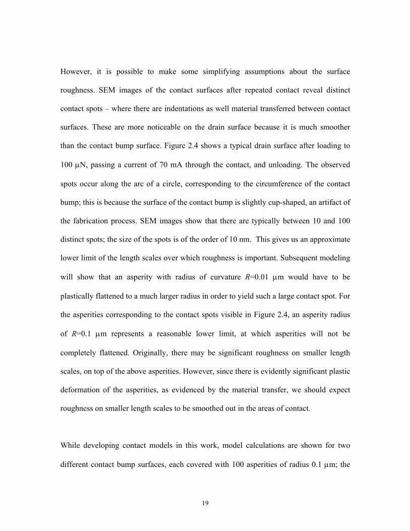
than the contact bump surface. Figure 2.4 shows a typical drain surface after loading to
100 µN, passing a current of 70 mA through the contact, and unloading. The observed
spots occur along the arc of a circle, corresponding to the circumference of the contact
bump; this is because the surface of the contact bump is slightly cup-shaped, an artifact of
the fabrication process. SEM images show that there are typically between 10 and 100
distinct spots; the size of the spots is of the order of 10 nm. This gives us an approximate
lower limit of the length scales over which roughness is important. Subsequent modeling
will show that an asperity with radius of curvature R=0.01 µm would have to be
plastically flattened to a much larger radius in order to yield such a large contact spot. For
the asperities corresponding to the contact spots visible in Figure 2.4, an asperity radius
of R=0.1 µm represents a reasonable lower limit, at which asperities will not be
completely flattened. Originally, there may be significant roughness on smaller length
scales, on top of the above asperities. However, since there is evidently significant plastic
deformation of the asperities, as evidenced by the material transfer, we should expect
roughness on smaller length scales to be smoothed out in the areas of contact.
While developing contact models in this work, model calculations are shown for two
different contact bump surfaces, each covered with 100 asperities of radius 0.1 µm; the
19
Figure 2.4 SEM micrograph showing close-up of the drain contact surface on a
microswitch that was loaded to a force of 100 µN per contact bump and then unloaded.
The scale in the right hand bottom corner shows 10 graduation marks 0.1 µm apart.
smoother surface has a Gaussian asperity height distribution with standard deviation (σ)
= 0.01 µm, and the rougher surface has σ= 0.1 µm. After the final model has been
obtained, at the end of Chapter 3, model calculations are shown for a range of asperity
radii, and for a range of values of σ; the effects of these parameters on the model results
are then discussed.
When a surface with asperities is pressed a certain distance into the flat surface, the load
borne by each asperity and the size of the corresponding contact spot has to be
determined using an appropriate (elastic or plastic) deformation model. In section 2.2, I
discuss the measurement of material properties used in the deformation model. The
deformation model for a single asperity is discussed in sections 2.3 and 2.4, followed by a
model with multiple asperities of different heights, resulting in multiple contact spots of
different sizes (section 2.5).
20

2.2 Measurement of mechanical properties
The values of hardness and elastic modulus used in the models in this section were
obtained from nano-indentation measurements. Samples used for measurements were die
from a silicon wafer sputtered with 0.2 µm gold on top of 1 µm SiO2 at Northeastern
University. The measurements were performed at Hysitron Incorporated, Minneapolis. A
Berkovich diamond indenter was used to indent the sample to a depth of 8.6 nm. The
hardness was defined as the ratio of the maximum load to the projected area. To calculate
the modulus of elasticity, a “reduced” modulus, Er, was calculated from the unloading
half-cycle, as A
SEr2
π= , where S is the unloading stiffness
dhdP
, and A is the
projected contact area. From 10 separate measurements, the average values of hardness
and reduced modulus were reported as 2.2 GPa and 110 GPa respectively, with standard
deviations of 0.1 GPa and 9 GPa respectively.
The reduced modulus is related to the elastic moduli of the sample and the indentor as
( ) ( )i
i
s
s
r EEE
22 111 νν −+
−= , where the s and i subscripts refer to the sample and indentor
respectively. For the indentor, I used the elasticity and Poisson’s ratio values supplied by
Hysitron, 1140 GPa and 0.07 respectively. The Poisson’s ratio of the sample was
assumed to be 0.5 – therefore the elastic modulus of the sample can be calculated to be 91
GPa.
21

The same values of hardness and elastic modulus were used for the other contacting body
(the contact bump), since corresponding measured values were not available.
2.3 Contact between sphere and flat
At small contact forces, the deformation of the contacting bodies is elastic, and therefore,
fully reversible. Consider the contact between a single spherical asperity of radius R, and
a flat surface. Let the moduli of elasticity of the contacting bodies be denoted by E1 and
E2, respectively, and their Poisson's ratios by ν1 and ν2 respectively. The effective
modulus of elasticity is defined as K, where
)11(431
2
22
1
21
EEKνν −
+−
= (2.1)
In our case, both contact bodies are assumed to have the same material properties,
E1=E2=91 GPa, and ν1=ν2=0.5. Therefore, EK98
= =80.9 GPa.
In the absence of any applied contact force, the sphere and the flat touch at a single point
(Figure 2.5 (a)). Under an applied contact force F, the contacting bodies are pressed
against each other, so that corresponding points on the surfaces of the bodies far away
from the contact interface approach each other by a distance α. The bodies are brought
into contact over a spherical section (Figure 2.5 (b)). The projection of this section on the
undeformed flat surface is a circular contact spot of radius a. The deformation of the
contact bodies and the radius of the contact spot are given by the well-known Hertz
model. The model is based on the following assumptions:
1. a<<R;
22

2. there is no friction at the interface;
3. there is no tensile stress in the area of the contact.
Using these assumptions, it can be shown (for example, Johnson(1985), that the radius of
the contact spot, a, is related to the contact force F as
a FRK
= ( ) /1 3 (2.2)
The contact radius a is related to the vertical deformation α as
a R= α (2.3)
As the contact force increases, there is a gradual transition from elastic to plastic
deformation over a range of forces. The transition is usually referred to as the elasto-
plastic regime. If the von Mises criterion [Timoshenko 1951] is applied to stresses in the
F=0
Vertical Deformation
ContactRadius
F
(a) (b)
Figure 2.5 Schematic representation of contact between a spherical asperity and a flat
surface. In the absence of any contact force, contact occurs at a single point (a). Under a
force F, the projection of the area of contact on the undeformed flat surface is a circular
contact spot (b).
23

contact bodies for contact between a sphere and a flat, it is found that the condition for
plastic yielding is first reached at a mean contact pressure of Fa
Yπ 2 11= . . The plastic zone
is initiated at points within the contacting bodies, on the contact axis and about 0.5a from
the contact interface, where a is the contact radius [Timoshenko 1951]. As the contact
force increases, the plastic zone expands outwards, in the process reaching the surface
and extending over the entire contact area, and the deformation becomes fully plastic.
Away from the contact interface, the plastic zone merges into an elastic “hinterland”. The
elastic deformation produces the counter pressure that balances the contact load, and
vanishes when the contact load is removed. When full plasticity is reached, the contact
pressure becomes independent of the contact load, and equal to the hardness H:
YHaFpm 32 ===
π,
(2.4)
The contact area in the intervening elasto-plastic regime has been given semi-empirically
by Studman [Studman 1976] (for ν=0.5):
)3
ln321(2 YR
EaYaFpm +==
π,
(2.5)
Full plasticity is reached (that is, the contact pressure becomes equal to 3Y) when
ERYaa p 60≈= , in agreement with experiments. However, in the Studman model, the
transition from elastic to elasto-plastic deformation (when the elastic and elasto-plastic
models both give the same contact radius at the same contact force) occurs at ,
instead of 1.1Y. Maugis and Pollock (1984) propose a modification of the Studman
model, in order to satisfy the von Mises criterion, and still obtain the correct value of a
Ypm 9.0=
p
at which contact becomes fully plastic. Following this approach, we have:
24
)9.3
ln7.01.1(YR
EaYpm += , (2.6)
A simpler, and less physically realistic model is an elastic-perfectly plastic model, with
an abrupt transition from the elastic to the plastic. In this case, equation 2.2 is assumed to
be valid until the contact pressure becomes equal to the hardness H, at a contact radius
ERY
KRYa p 113 ≈= π , and equation 2.4 holds beyond this point. Figure 2.6 shows the
radius of the contact spot as a function of the contact force, using both the modified
Studman model and the simple elastic-plastic model. The latter characteristic shows a
change in slope at a force of 0.55 µN, corresponding to the elastic-to-plastic transition.
The modified Studman model predicts a gradual transition from perfectly elastic
deformation up to a force of 0.025 µN to perfectly plastic deformation at a force of 16.3
µN.
The ultimate version of the contact model (including adhesion due to surface forces),
developed in Chapter 3, is based on the modified Studman elasto-plastic deformation
model. However, in the simpler adhesionless model developed in the rest of this chapter,
the simple elastic-perfectly plastic model is used. This is to make it easier to develop a
model of subsequent contact, after the contacts have been loaded and unloaded one or
more times. This is discussed in greater detail in following sections.
25

Figure 2.6 Modeled variation of contact spot radius with load when a single 0.1 micron
asperity is pressed into a flat surface, as given by the deformation model of Studman,
modified by Maugis and Pollock.
Force (N)10-8 10-7 10-6 10-5 10-4
Con
tact
radi
us (m
)
10-9
10-8
10-7
elastic-fully plastic model, elastic elastic-fully plastic model, plasticmodified Studman model, elasticmodified Studman model, elasto-plasticmodified Studman model, plastic
2.4 Deformation during subsequent contacts
The equations in the previous section describe what happens during contact between an
asperity and the flat for the first time. The asperities on the contact bump have been
assumed to be spherical, with radius R, and the surface of the drain has been assumed to
be flat. If the contact force is sufficient to cause some plastic deformation during contact,
there is a “flattening” of the asperities, and corresponding concavities are formed in the
drain. Upon unloading, the elastic deformation is recovered, but the plastic deformation,
persists, so that the asperity now has some radius R1<R’, and the concavity in the drain
has a radius -R2, R2>R’.
A simple and commonly accepted assumption is that all of the plastic deformation occurs
during the first contact between the sphere and the flat surface. Finite element simulations
26

of a perfectly plastic deformation model have shown that this is a good assumption in this
situation [Kral 1993]. This assumption makes it straightforward to calculate the deformed
asperity radius in an elastic-perfectly plastic deformation model. Consider a contact
subjected to a contact force Ff, resulting in formation of a contact spot of radius af by
purely plastic deformation (equation 2.4). Subsequent contacts with a contact force less
than or equal to Ff, are governed by the Hertzian solution for elastic contact between a
sphere and a concave spherical surface. The Hertz equations for elastic contact between a
sphere and a flat are still applicable to this case, if the asperity radius R is replaced by an
effective radius Reff,
1 11 2R R Reff
= − 1 , (2.7)
Re-loading the contact with a force equal to Ff results in elastically forming a contact of
the same radius af as given by the earlier plastic loading, so that (from the Hertz relation
for elastic contact, equation 2.2), the effective radius of curvature is given by:
f
feff F
KaR
3
= . (2.8)
The amount of elastic recovery (αr) in the height of the asperity during the first unload
half-cycle can also be calculated. Since we assume that after the first load-unload cycle,
subsequent load-unload cycles are purely elastic and reversible, the elastic recovery must
be equal to the vertical deformation when elastically loading to Ff during subsequent
cycles. That is,
efffr Ra 2=α . (2.9)
27

Figure 2.7 Modeled variation of effective asperity radius Reff as a function of the
maximum load on the first cycle. Initial asperity radius is 0.1 micron
Force (N)10-7 10-6 10-5 10-4
Effe
ctiv
e as
perit
y ra
dius
(mic
ron)
0.0
0.5
1.0
1.5
2.0
Figure 2.7 shows the calculated variation in Reff with Ff for an asperity with initial radius
of curvature, R=0.1 micron. Up to a load of 0.08 µN, the deformation is elastic, and there
is no permanent change in the radius of curvature; beyond this load, there is a progressive
increase in Reff. Figure 2.8 shows the effect of initial plastic loading up to 20 µN, and 50
µN, on the contact spot radius versus contact force characteristic. Initial loading up to 20
µN results in an effective radius of curvature of 0.63 µm, and the contact radius at that
load is 0.054 µm. The characteristic for subsequent loading expectedly shows elastic
deformation up to 20 µN, and shows the same contact radius of 0.054 µm at that force.
Initial loading up to 50 µN results in Reff =1 µm and a contact radius of 0.085 µm, and
similarly shows elastic deformation up to 50 µN on subsequent cycles.
28

2.5 Multiple asperity model
We now have a model for a how a single asperity deforms under a certain load. Let us
consider a model with a distribution of multiple asperities on the surface of the contact
bump. Our model is based on a model proposed by Chang, Etsion and Bogy [Chang
1988]. In turn, the CEB model is a refinement of the asperity-based model introduced by
Greenwood and Williamson [Greenwood 1966], in which the rough surface is
represented by a collection of spherical asperities with identical end radii, whose heights
have a statistical distribution. The asperities are assumed to be independent of each other,
that is, the load on one asperity does not affect the deformation of another. The area of
contact for each asperity in the Greenwood-Williamson model is calculated from the
Hertz theory of elastic deformation, even though at a particular contact force the loads on
some of the asperities may have exceeded the elastic limit so that the asperities deform
plastically. The CEB model calculates the deformation of a plastically deformed asperity
on the basis of volume conservation of a certain control volume of the asperity. In the
following paragraphs, we briefly explain the equations governing the above model.
29

Figure 2.8 Modeled variation of contact spot radius with load on the first cycle, and on
subsequent cycles, after the contact has been previously loaded up to 20 µN and 100 µN
respectively. The asperity radius is initially 0.1 micron. The effective asperity radius is
0.61 micron after loading to 20 µN, and 0.95 micron after loading to 50 µN.
Contact Force (N)10-7 10-6 10-5 10-4
Con
tact
spo
t rad
ius
(m)
10-9
10-8
10-7
10-6
First cycleAfter prior loading to 20 µNAfter prior loading to 50 µN
First consider one of the spherical asperities in contact with the flat surface, under a load
F. Depending on the load, the deformation is either elastic or perfectly plastic. For elastic
deformation, the radius of the resulting contact spot is given by Equation 2.2, and the
vertical deformation of the asperity is given by Equation 2.3.
Plastic yielding is assumed to occur when the average pressure at the contact interface
equals H, the hardness of the contacting material. The vertical deformation of the asperity
at this transition is given by
30

α πc
HK
R= ( )2 . (2.10)
In the plastic region, the average pressure on an asperity is assumed to be H, so that the
contact force on the asperity is
F Ha= π 2 . (2.11)
In fully plastic deformation, the vertical deformation α is related to the contact radius a
as αR2=a , as against a in elastic deformation. In order to reflect this transition,
based on conservation of volume arguments, the vertical deformation is given in the CEB
model as:
R= α
a R c= −α αα
( )2 , α α> c (2.12)
Hence, for a given vertical deformation α, the force on each asperity as well as the radius
of the corresponding contact spot can be determined.
Now consider a rough surface with N asperities, each with an end radius of curvature R,
and heights z1 > z2 > … > zN (Figure 1.1). Let the separation between the reference planes
be d for a given contact force F, such that zn > d > zn+1. Then asperities 1,2,...,n come into
contact. The vertical deformation of asperity i is given by
.dzii −=α (2.13)
For a given separation between the reference planes, the force on each asperity, and the
radius of each of the corresponding contact spots can be obtained using the previously
stated equations.
31

As mentioned earlier, because of the variability of the roughness of the contact surfaces,
contact spot radii are calculated for surfaces with 2 different roughness values - σ = 0.01
µm, and 0.1 µm, where σ is the standard deviation in the asperity heights. Figure 2.9
shows the number of contact spots as a function of the contact force for each of these
surfaces (2.9 (a) and 2.9 (c) for σ = 0.01 µm and 0.1 µm respectively) and the variation of
a few different asperity contact radii (2.9 (b) and 2.9 (d) respectively). For the smoother
surface, 6 asperities are predicted to be in contact at a contact force of 20 µN, increasing
to 20 contacting asperities at 100 µN. For the rougher surface, the number of contacting
asperities at the above forces is 2 and 3 respectively.
Figure 2.10 shows the same characteristics for two cases – previously unloaded contacts,
and contacts that were previously loaded to 100 µN and unloaded. Up to 100 µN, the
contact spot radii of the previously loaded contacts vary more gradually with the contact
force than the corresponding spot radii of previously unloaded contacts, since the
asperities have been flattened by the previous load cycle. At larger forces, the two sets of
characteristics are identical.
32

Force (N)10-6 10-5 10-4 10-3
Num
ber o
f con
tact
spo
ts
0
10
20
30
40
50
60
70
80
90
100
(a)
(b)
Force (N)10-6 10-5 10-4 10-3
Num
ber o
f con
tact
spo
ts
0
2
4
6
8
10
12
14
16
18
20
(c)
(d) Figure 2.9 Modeled variation of number of contacting spots, and contact spot radii with
contact force for a surface with roughness σ=0.01 micron ((a) & (b)), and σ=0.10 micron
((c) & (d)). The initial asperity radius is 0.1 micron.
Contact Force (N)10-6 10-5 10-4 10-3
Con
tact
spo
t rad
ius
(m)
10-9
10-8
10-7
10-6
Asperity 1Asperity 2Asperity 5Asperity 10
Contact Force (N)10-6 10-5 10-4 10-3
Con
tact
spo
t rad
ius
(m)
10-9
10-8
10-7
10-6
Asperity 1Asperity 2Asperity 5Asperity 10Asperity 50
33

Force (N)10-6 10-5 10-4 10-3
Num
ber o
f con
tact
spo
ts
0
10
20
30
40
50
60
70
80
90
100Previously unloadedPreviously loaded to 100 µN
(a)
(b)
Force (N)10-6 10-5 10-4 10-3
Num
ber o
f con
tact
spo
ts
0
2
4
6
8
10
12
14
16
18
20
No previous loadingPreviously loaded to 100 µN
(c)
(d)
Figure 2.10 Modeled variation of number of contacting spots, and contact spot radii
with contact force, when the contact has previously been loaded to 100 µN and
unloaded. Figures 2.10 (a) and 2.10 (b) correspond to a surface with roughness
σ=0.01 micron, and 2.10 (c) and 2.10 (d) correspond to a surface with σ=0.10 micron.
The same characteristics for a previously unloaded contact (from Figure 2.9) are also
shown for comparison.
Contact Force (N)10-6 10-5 10-4 10-3
Con
tact
spo
t rad
ius
(m)
10-9
10-8
10-7
10-6Asperity 1, no previous loadingAsperity 1, contacts previously loaded to 100 µNAsperity 2, no previous loadingAsperity 2, contacts previously loaded to 100 µNAsperity 5, with/without previous loading to 100 µN
Contact Force (N)10-6 10-5 10-4 10-3
Con
tact
spo
t rad
ius
(m)
10-9
10-8
10-7
10-6 Asperity 1, no previous loadingAsperity 1, contact previously loaded to 100 µNAsperity 5, no previous loadingAsperity 5, contact previously loaded to 100 µNAsperity 50, with/without previous loading to 100 µN
2.6 Contact Resistance
The remaining step is to determine the contact resistance, given a certain number of
contact spots of known radii. We first consider the contact resistance of a single spot of a
34

given radius a, separating 2 semi-infinite bodies of resistivity ρ, and then study the more
general problem with multiple contact spots of different sizes, and finite contacting
bodies. In the single-spot case, the contact resistance arises from two different
phenomena. If the radius a is small compared to the electron mean free path length le of
the material, the resistance of the contact spot is dominated by the Sharvin mechanism
[Jansen 1980], in which electrons are projected ballistically through the contact spot
without being scattered. In this case,
R lacon
e=43 2
ρπ
(2.14)
On the other hand, if the radius is much larger than the mean free path length, the
resistance is dominated a diffuse scattering mechanism, and is given by the Maxwell
spreading resistance formula [Holm 1967]:
Racon = ρ
2 (2.15)
Wexler [Wexler 1966] has given a solution of the Boltzmann equation, using the
variational principle for resistance of a circular contact spot separating semi-infinite
bodies. This results in a simple interpolation formula which can account for the transition
between the Maxwell and Sharvin regimes:
R la
l aacon
ee= +
43 22
ρπ
υ ρ( / ) . (2.16)
35

K=le/r0.001 0.01 0.1 1 10 100
ν
0.65
0.70
0.75
0.80
0.85
0.90
0.95
1.00
1.05
Figure 2.11 Interpolation factor ν to account for transition from Sharvin to Maxwell
regime (from Wexler[1966]).
ν is a slowly varying function of the ratio le/a, with ν(0)=1, and ν(∞)=0.694 (Figure
2.11).
In general, multiple asperities come into contact, resulting in multiple contact spots of
varying sizes. The effective contact resistance arising from the contact spots depends on
the radii of the spots (given by the contact area model discussed previously) and the
distribution of the spots on the contact surface. A lower bound can be obtained on the
contact resistance by assuming that contact spots are independent and conduct in parallel
(this is equivalent to the exact solution when the radii of the contact spots are small
compared to the separation between the spots). Denoting the contact resistance of spot i
as Rcon,i,
1 1/ /, ,R Rcon lb con ii
= ∑ (2.17)
36

An upper bound can be obtained on the contact resistance by computing the resistance of
a circular spot of radius aeff, and of area equal to the total area of all the individual contact
spots combined ( ∑= 2ieff aa ).
R la
l aacon ub
e
effe eff
eff, ( / )= +4
3 22ρ
πυ ρ (2.18)
This upper bound is equivalent to the exact solution when all the conducting spots
become large enough to merge into a single conducting spot.
By putting together the contact resistance model given by equations 2.17 and 2.18 with
the contact spot radii against force characteristics obtained in section 2.5, we can
determine lower and upper bounds on the contact resistance, as a function of the contact
force, for a given surface roughness. For model calculations, the resistivity ρ of the drain
and beam layers was measured using Van der Pauw structures on the device wafer, as
6.75x10⁻⁸ Ω-m and 3.85x10⁻⁸ Ω-m respectively. Since the total contact resistance is the
sum of the contact resistances in the two contact bodies, we use the average of the
measured resistivity values in equations 2.17 and 2.18. There is some inaccuracy in doing
this, since on the underside of the contact bump is a layer of sputtered gold, 0.1 µm thick.
The resistivity in this layer is unknown, but probably similar to that in the drain.
However, as we will see, there is sufficient uncertainty in calculating the contact
resistance that this error is not very important. Figure 2.12(a) shows the calculated
dependence of contact resistance on contact force for two surfaces, one with σ=0.1 µm,
and the other with σ=0.01 µm. The upper bound characteristic, which depends only on
the total contact area, appears to be identical for both surfaces. This is because at low
37

contact forces, only a single asperity is in contact in either case, and at high forces, all the
asperities usually deform plastically, so that the total contact area is the same for both
surfaces. Figure 2.12(b) shows the calculations for switch contacts which were
previously loaded to 100 µN and unloaded, and deformation is consequently purely
elastic. In this case, too, the upper bound characteristic is independent of the surface
roughness - although there is no longer any plastic deformation, the contact area is
determined by the previous plastic deformation.
2.7 Effect of finite contact geometry
The contact resistance expressions of equations 2.17 and 2.18 are based on an ideal
contact geometry – a circular contact spot separating two semi-infinite contacting bodies.
One of the contacting bodies in the microswitch is the drain electrode. Since the drain
thickness – 0.2 micron – is comparable to the contact area, the semi-infinite idealization
does not appear to hold. To determine the error caused by making the semi-infinite
assumption, the contact geometry of Figure 2.13 was simulated, by a finite element
solution of the Maxwell model. For a contact spot radius a=0.1 micron, the Maxwell
contact resistance is Racon = ρ
2 . The finite element simulation gives a
Rcon 207.1 ρ
= .
The error introduced by the assumption in the Sharvin model was not evaluated.
38

(a) (b)
Figure 2.12 Modeled contact resistance vs contact force characteristics, on the first
cycle (a), and after the switch has previously loaded to 100 µN and unloaded (b). In
each graph, the upper bounds for the two values of σ nearly coincide.
Contact Force (N)10-7 10-6 10-5 10-4
Con
tact
Res
ista
nce
(Ohm
s)
10-2
10-1
100
101
102
σ=0.01 micron, lower bound σ=0.01 micron, upper bound σ=0.1 micron, lower bound σ=0.1 micron, upper bound
Contact Force (N)10-7 10-6 10-5 10-4
Con
tact
Res
ista
nce
(Ohm
s)
10-2
10-1
100
101
102
σ=0.01 micron, lower bound σ=0.01 micron, upper bound σ=0.1 micron, lower bound σ=0.1 micron, upper bound
1.8 Measured contact resistance
Contact resistance was measured using a microswitch design with an extra pair of
terminals which allow the voltage across the contact to be measured (Figure 2.14). Figure
2.15 shows the contact resistance of a microswitch, measured as a function of the gate-to-
source actuation voltage. For a previously untested microswitch, the contact resistance is
0.5 Ω - 1 Ω for actuation voltages up to 90 V, and decreases gradually as the actuation
voltage is increased. As the switch is cycled by turning it on and off repeatedly, its
contact resistance decreases. The switch in Figure 2.15 has a contact resistance of the
order of 0.1 Ω. after 1000 test cycles. However, it now also varies less with the actuation
voltage than before.
39

I=0
I=0
V= 1 Volt
V= 0
φ=0.1 µmφ=6 µm
φ=10 µm
Figure 2.13 Contact model used to study deviation from ideal constriction. The upper
hemisphere represents the beam, and the lower cylinder represents the drain electrode.
The dotted-line circle is a contact spot at their interface, diameter 0.1 micron.
In order to compare the measured contact resistance with the contact resistance model,
it is necessary to map the actuation voltage to the contact force. This can be done by
modeling the microswitch as a beam which is clamped at its fixed end, and simply
supported at its free end (Figure 2.16). The Euler-Bernoulli beam equations are used to
determine the beam deflection and contact force boundary condition, assuming a certain
distributed electrostatic force acting on the beam. In turn, the new electrostatic force is
determined as a function of the beam shape. The two steps are repeated iteratively, until
40

V
Contact bump
Drain 1
Drain 2
Source 1
Source 2
Figure 2.14 Microswitch geometry used to measure contact resistance. Current
(represented by the broken lines) is forced between one pair of source and drain
terminals, and the other pair of source and drain terminals is used to measure the
voltage across the contact. The contact bump on the lower surface of the beam is not
visible in this micrograph.
the solution converges. Figure 2.17 shows the modeled variation of contact force with
gate voltage for the microswitch shown in Figure 2.14. An actuation voltage of 90 V is
seen to correspond to a contact force of approximately 100 µN.
Using this model, the measured contact resistance characteristics of Figure 2.15 are
plotted as a function of contact force in Figures 2.18 (a) and (b). The lower and upper
bounds predicted by the contact resistance model for a previously uncycled switch are
shown for comparison in Figure 2.18 (a), and the contact resistance bounds for a switch
previously subjected to a 100 µN load are shown in Figure 2.18 (b). The initial measured
resistance is 0.3-0.6 Ω higher than predicted, and its dependence on contact force has
roughly the same shape as predicted. The measured resistance after 1000 switch cycles is
much less sensitive to the contact force than predicted by the model, and
correspondingly, much lower than predicted at low contact forces.
41

Figure 2.15 Measured contact resistance as a function of actuation voltage, for a
previously untested switch, and after the same switch had been cycled 10 times and
1000 times with an actuation voltage of 78 V and a current of 4 mA.
Avtuation Voltage (V)0 20 40 60 80 1
Con
tact
Res
ista
nce
(Ohm
s)
0.0
0.2
0.4
0.6
0.8
1.0
1.2
1.4
InitialAfter 10 cyclesAfter 1000 cycles
00
FE
Contact ForceR1
M
Gate
Figure 2.16 Beam model of microswitch in closed position. The fixed end of the beam is
assumed to be clamped, and the contact bump is assumed to be simply supported at the
drain.
42

It seems reasonable to assume that the lower contact resistance after cycling the
switch is a result of repeated “scrubbing” of the contact surfaces resulting in a cleaner
contact interface. However, this does not explain the reduced sensitivity to the contact
force. The reason for this phenomenon appears to be adhesion between the contact
surfaces. If there is significant adhesion between the contact surfaces, this would tend to
hold them closed while the contacts are being unloaded, reducing the sensitivity of the
contact resistance to the contact force. It would also result in a hysteresis - the switch
would open at a smaller actuation voltage than that at which it closes. This is indeed
observed in measurements – Figure 2.19 shows the measured contact resistance of a
switch when the actuation voltage is increased from 0 to 90 V, and then decreased back
to 0 (this is actually the same measurement as shown in Figure 2.18 (b) – only the loading
half-cycle was shown in Figure 2.18 (b)). The switch closes at 65 V, and opens at 45 V.
Figure 2.17 Modeled variation of contact force with gate-to-source actuation voltage
for the microswitch geometry of Figure 1.5.
Actuation Voltage (V)60 80 100 120 140
Con
tact
For
ce (µ
N)
0
50
100
150
200
250
300
43

(a) (a) (b) (b)
Figure 2.18 Comparison of measured contact resistance with the contact resistance
model. The measured characteristics are the ones shown in Figure 2.15: 2.18(a) shows
the measured resistance of a previously untested switch, and (b) shows the measured
resistance after 1000 switch cycles. The modeled contact resistance for a previously
untested switch is shown for comparison in 2.18(a), and the modeled contact resistance
for a contact previously subjected to 100 µN is shown in (b).
Contact Force (N)10-6 10-5 10-4
Con
tact
resi
stan
ce (O
hms)
0.0
0.2
0.4
0.6
0.8
1.0
1.2
1.4Model, σ=0.01 µm,lower boundModel, σ=0.1 µm,lower boundModel, upper boundMeasurement (initial)
Contact Force (N)10-6 10-5 10-4
Con
tact
resi
stan
ce (O
hms)
0.0
0.2
0.4
0.6
0.8
1.0
1.2
1.4 Model, σ=0.01 µm,lower boundModel, σ=0.1 µm,lower boundModel, upper boundMeasurement (after 10 cycles)Measurement (after 1000 cycles)
Figure 2.19 Hysteresis in contact resistance measurements. Contact resistance was
measured first while the actuation voltage was increased from 0 to 90 V, and then while
it was decreased back to 0.
Figure 2.19 Hysteresis in contact resistance measurements. Contact resistance was
measured first while the actuation voltage was increased from 0 to 90 V, and then while
it was decreased back to 0.
Actuation Voltage (V)0 20 40 60 80 1
Con
tact
Res
ista
nce
(Ohm
s)
0.0
0.2
0.4
0.6
0.8
1.0
1.2
1.4
00
44

Apart from contact adhesion, another possible reason for the observed hysteresis is
the well-known mechanical instability of electrostatically actuated structures. This results
in a pull-in of the beam at some critical beam-gate, which is different in the open and
closed positions of the switch. However, the Euler-Bernulli beam model predicts that
there is little or no hysteresis in the switch arising from mechanical instability. Also, the
amount of hysteresis is found to change as a switch is cycled. There is also a strong
correlation between the contact resistance and the actuation voltage at which the switch
opens, indicating that a cleaner contact results in more hysteresis (Figure 2.20).
Clearly, a major element missing from the contact resistance model at this stage is
contact adhesion. In Chapter 3, I will present a contact resistance model that includes
contact force, and study different aspects of contact adhesion and the resulting hysteresis.
Resistance (Ohms)0.1 1
Turn
-off
Volta
ge (V
olts
)
10
20
30
40
50
60
Figure 2.20 Measured turn-off voltage of a group of 7 microswitches; each device
was cycled 106 times, and its contact resistance and turn-off voltage was measured at
intervals while cycling. The measured turn-off voltage is plotted as a function of
contact resistance.
45

References
[Greenwood 1966] J. A. Greenwood and J.B.P. Williamson, "Contact of Nominally Flat
Surfaces", Proceedings of the Royal Society (London), Vol. 295, pp. 300-319, 1966.
[Greenwood 1971] J. A. Greenwood and J. H. Tripp, “The Contact of Two Nominally
Flat Rough Surfaces”, Proceedings of Institution of Mechanical Engineers, Vol. 185,
625-633.
[Bush 1975] A. W. Bush, R. D. Gibson and T. R. Thomas, “The Elastic Contact of a
Rough Surface”, Wear, Vol. 35, pp. 87-111, 1975.
[Timoshenko 1951] S. Timoshenko and J. Goodier, Theory of Elasticity, McGraw Hill
(New York), 2nd ed., 1951.
[Bhushan 1998] B. Bhushan (ed.), Handbook of Micro/Nanotribology, CRC Press (Boca
Raton), 2nd ed., 1998.
[Williams 1991] E. D. Williams and N. C. Bartlett, “Thermodynamics of Surface
Morphology”, Science, Vol. 251, pp. 393-400, 1991.
[Majumdar 1990] A. Majumdar and B. Bhushan, “Role of Fractal Geometry in
Roughness Characterization and Contact Mechanics of Surfaces”, ASME Journal of
Tribology, Vol. 112, pp. 205-216, 1990.
[Studman 1976] C. J. Studman, M. A. Moore and S. E. Jones, Journal of Physics D,
Applied Physics, Vol. 10, pp. 949-958, 1976.
[Kral 1993] E. R. Kral, K. Komvopoulos, and D. B. Bogy, “Elastic-Plastic Finite Element
Analysis of Repeated Indentation of a Half-Space by a Rigid Sphere”, Journal of Applied
Mechanics, Vol. 60, pp. 829-841, 1993.
[Chang 1988] W. R. Chang, I. Etsion, and D.B. Bogy, "An Elastic-Plastic Model for the
Contact of Rough Surfaces", Journal of Tribology, Vol. 109, pp. 257-263, 1988.
[Jansen 1980] A. G. M. Jansen, A. P. van Gelder, and P. Wyder, “Point-Contact
Spectroscopy in Metals”, Journal of Physics, Vol. C13, pp. 6073-6118, 1980.
[Holm 1967] R. Holm, Electric Contacts, Springer-Verlac (New York), 1967.
[Wexler 1966] G. Wexler, “The Size Effect and the Non-Local Boltzmann Transport
Equation in Orifice and Disk Geometry”, Proceedings of Physical Society, Vol. 89, pp.
927-941, 1966.
46

[Johnson 1985] K. L. Johnson, Contact Mechanics, Cambridge University Press,
Cambridge, MA, 1985.
47


![Surface separation and contact resistance considering ...jacksr7/Wilson-ECRsurfaceseperation-2009.pdf · Ciavarella et al. [20] also extended their 2D stacked model of contact between](https://img.pdfslide.us/doc/110x75/5e79204836d8c626d56d8256/surface-separation-and-contact-resistance-considering-jacksr7wilson-ecrsurfaceseperation-2009pdf.jpg)