Embed Size (px)
Citation preview
Evaluation of Contact Resistance of Silver-Loaded
Epoxy with Aluminized Backplane of Silicon
Microstrip Sensors
T. Kohriki, A. Mochizuki, Y. Ikegami, Y. Unno, S. Terada, and K. Hara
Abstract-Some modules of the ATLAS silicon strip detector (SCT) exhibited a significantly higher effective bias resistance than we had expected. About 20 % of the barrel modules, for
instance, showed such a resistance of 40 k or higher. We have tried to identify causes of this high resistance as well
as to find a remedy if necessary. As for the SCT modules, the bias connection is made with silver-loaded epoxy to the aluminized backplane of the silicon sensors.
It was identified that the contact of the silver-loaded epoxy to the surface of the aluminized backplane sometimes provoked the high resistance. Fortunately, however, it automatically cures in practice by applying a usual bias voltage, to become harmlessly small of a few ten ohms.
I. INTRODUCTION
Many modules of silicon strip detectors (SCT), 2112 for the
barrel and 1976 for the endcaps, were fabricated and
assembled as a central tracker of ATLAS for a LHC
experiment [1].
While testing the modules after assembled in cylinders
(barrel) and disks (endcaps), some modules exhibited a
significantly higher effective bias resistance than we had
expected [2]. They were spotted as checking continuities of
cablings and connections by applying a small forward voltage
to the modules. In fact about 20 % of the barrel modules, for
instance, showed such a resistance of 40 k or higher, as high
as a few hundred k , in comparison with an expectation of
about 11 k which was an overall resistance of the biasing
circuit (see Fig. 3).
Concerns were raised particularly about a voltage drop to an
applied bias voltage after an exposure of a high radiation dose
which would induce a high leakage current of the modules.
II. SCT BARREL MODULE AND BIAS CONNECTION
The SCT barrel module [3] is made of four sensors of 64
mm x 64 mm each, a pair of two are glued on a TPG
baseboard on top and bottom. A Cu/Polyimide
flex-circuit-based hybrid is wrapped around the
sensor-baseboard sandwich.
Manuscript received November 4, 2007.
T. Kohriki, Y. Ikegami, Y. Unno and S. Terada (e-mail:
[email protected]) are with Inst. of Particle and Nuclear Studies, High
Energy Accelerator Research Org., KEK, Tsukuba, Ibaraki 305-0801 Japan.
A. Mochizuki and K. Hara are with Institute of Pure and Applied Sciences,
University of Tsukuba, Tsukuba, Ibaraki 305-8571 Japan.
The sensors are a conventional p-strip in n-bulk with a
backside metallization of aluminum. The bias connections to
Fig. 1. ATLAS SCT barrel module
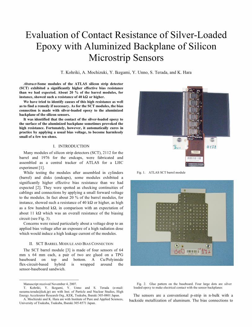
Fig. 2. Glue pattern on the baseboard. Four large dots are silver loaded epoxy to make electrical contact with the sensor backplanes
Fig. 3. Setup for continuity measurements Biasing scheme to sensors in SCT barrel module is illustrated.
the sensor backside are made through the TPG baseboard by
means of a silver loaded epoxy adhesive. Fig. 1 shows the
completed barrel SCT module, while Fig. 2 shows a glue
process of the sensors and baseboard. White dots on the black
baseboard are adhesives. The large four dots are silver-loaded
epoxy to make electrical contacts with a pair of the sensors to
be attached on top of the baseboard. Incidentally the many
small dots are a boron nitride doped epoxy adhesive.
As illustrated in Fig. 3 the bias circuit in the hybrid has a
resistance of 11.2 k , which should be registered in the
continuity measurements of the modules, if normal.
III. FORWARD BIASING AND DIODE CHARACTERISTIC
A part of complications arose in the resistance measurement
due to a diode characteristic of the sensors. In order to
measure the bias resistance some small forward voltage was
applied to the bias circuit through the hybrid.
Since we concerned an over-current to the sensor, the
measurement was tried with a small constant current of 10μA
at first, which turned out to be too low a voltage to fully turn
on the diode. As a result most of the module exhibited
significantly high resistance values.
In fact as we relaxed the current limit up to 1mA, majority
of the modules asymptotically reduced the resistance toward
the expected 11 k . Typical examples of them are shown in
Fig. 4.
In contrast, some modules showed such a peculiar behavior
in I-V measurements that the current, initially small, jumped
up suddenly to the normal as the applied voltage was raised
carefully in an isolated quiet condition. Then once it reached
to the normal current it remains the normal thereafter in the
repeated measurement as far as it was performed right after
the first one. Typical examples are shown in Fig. 5 and 6.
IV. CONNECTIONS WITH CONDUCTIVE ADHESIVE
As we focused on the most suspicious contacts, namely the
ones between the aluminized sensor back-plane and the TPG
with silver loaded epoxy, the hybrid and the other connections
were all bypassed. Then the four sensors of the module were
individually measured. Relevant connections in the setup are
illustrated in Fig. 7.
The results showed prominent jumping behaviors in I-V
curves in the first measurements. Fig. 8 shows an example in
Fig. 4. Module resistance as a function of forward bias current for
the normal modules (three modules: m751, m946, and m957)
Fig. 5. I-V relation of the high resistance module; There is a
current jump in the first measurement at 7 volts. It goes back to normal,
however, in the second measurement.
Fig. 6. I-V relation of a high resistance module; initially very high
resistance becomes normal at 3.5 volts with an abruptly current jump.
However, it behaves normally from the beginning in the second
measurement.
which four sensors of the module (m102) behaved rather
differently. One sensor (S1) was normal but the other three
(S2, S3, and S4) showed a transition from a high resistance to
a normal resistance around three and four volts. However, in
the second measurements, when performed right after the first
ones, the all sensors became normal and behaved smoothly as
shown in Fig. 9.
V. STUDIES WITH CONTROLLED SAMPLES
In order to investigate further the contact of the aluminized
sensor surface with the silver loaded epoxy, dedicated samples
shown in Fig. 10 were prepared. The square plates are pieces
of aluminized silicon cut from the actual sensor. A pair of
them are glued with a droplet of the silver loaded epoxy
placed at the center together with the boron nitride epoxy (four
white dots) and 200μm thick spacers placed at the four corners
(small squares). Copper leads are glued and wire bonded on
the aluminum surface.
Those samples were exposed to various environmental
conditions such as high temperature (50 C°) and either
nitrogen or air atmosphere during the tests.
As shown in Fig. 11, the measurements show a conspicuous
on-off behavior that an initially very high resistive contact
becomes conductive of a few ten ohms when an applied
voltage reaches at several volts. The highest and the lowest
resistance values in each measurement, which was taken place
once a day or a few days apart, are plotted in this figure. The
corresponding voltages at which the transition occurred in the
measurements are plotted in Fig. 12. As is prominent in these
figures, it usually goes back to a high resistive state in the next
measurement performed the day after, though its contact
always recovered at some point as the applied voltage
increased to several volts.
As a comparison the same samples but used Cu-clad G-10
plates were also measured. The results are shown in Fig. 13.
They show smooth behavior though with some variations. No
prominent hysteretic behavior nor any significant voltage
dependence to the resistance was observed.
Fig. 7 Setup for the resistance measurement between the sensor
backplane and the baseboard
Fig. 8 I-V behavior of the individual sensors in the initial
measurements
Fig. 9. I-V behavior of the individual sensors in the 2nd
measurements
Fig. 10. Controlled samples in fabrication
Far left: completed; Middle two: showing a glue pattern, as applied
(right), cured with a thin glass plate for monitoring purpose (left); Far
right: Aluminized silicon surface of the sample

VI. CONCLUSIONS
It was identified that the contacts of the silver-loaded epoxy
to the surface of the aluminized backplane of the silicon
sensor provoked high resistance. The combination of the
aluminized silicon surface and the silver-loaded epoxy is to be
an inferior choice to establish a secure electric contact.
Fortunately, however, it automatically cured by applying
several volts, which is much lower than the usual operating
bias voltage of a few hundred volts for the SCT, almost all of
the contacts became as small as a few ten ohms.
Therefore we can conclude that this high resistive aspect
found in the continuity checking is practically harmless in the
SCT operation.
VII. REFERENCES
[1] ATLAS Inner Detector Technical Design Report, Vol. I, ATLAS
TDR4, CERN/LHCC 97-16, and Vol. II, ATLAS TDR5, CERN/LHCC
97-17.
[2] Presented at ATLAS ID week at CERN on 27th February 2007 by J. R.
Carter.
[3] T.Kondo et al., Nucl. Instr. Meth. A485 (2002) 27-42; A. Abdesselam
et al, Nucl. Instr. Meth. A568 (2006) 642-671J.
Fig. 12 Long term test: applied voltage at which continuity was
recovered; one sample (#1) was kept in air while the other (#2) in
nitrogen atmosphere
Temperature was changed for some periods during the test.
Fig. 11 Long term tests of resistance behavior, initial resistance and
final (continuity recovered) ones Temperature was changed for some periods during the test.
Fig. 13 Copper samples: long term tests of resistance behavior
Temperature was changed for some periods during the test.


![EPOXY RESINS - Krishna districtkrishna.nic.in/PDFfiles/MSME/Chemical/EPOXY RESINS[1].pdf · EPOXY RESINS CONTENTS SECTION I ... PROJECT COST AND PROFITABILITY PROJECTIONS ... Epoxy](https://img.pdfslide.us/doc/110x75/5aa5b17b7f8b9ab4788d7c0f/epoxy-resins-krishna-resins1pdfepoxy-resins-contents-section-i-project.jpg)