Embed Size (px)
Citation preview

2005 International Conference on Characterization and Metrology for ULSI Technology
Source/Drain Junctions and Contacts for 45 nm CMOS and Beyond
Mehmet C. Ozturk
North Carolina State UniversityDepartment of Electrical and Computer Engineering

2005 International Conference on Characterization and Metrology for ULSI Technology
Outline• Series Resistance Challenges• SiGe Source/Drain Technology• Local Strain for Enhanced Mobility• Ultra-thin SOI & FINFET

2005 International Conference on Characterization and Metrology for ULSI Technology
Extension Structure
Junction &
Silicide Scaling
Silicide scaling cannot continue forever:
1) Leaky Junctions
2) Agglomeration
2005 International Conference on Characterization and Metrology for ULSI Technology
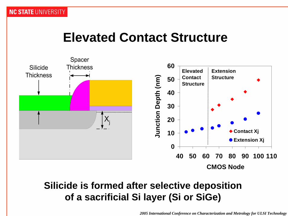
Elevated Contact Structure
0
10
20
30
40
50
60
40 50 60 70 80 90 100 110CMOS Node
Junc
tion
Dep
th (n
m)
Contact XjExtension Xj
ExtensionStructure
ElevatedContactStructure
Silicide is formed after selective deposition of a sacrificial Si layer (Si or SiGe)

2005 International Conference on Characterization and Metrology for ULSI Technology
Parasitic Source/Drain ResistanceThe Primary Source/Drain Challenge
0
200
400
600
800
1000
1200
1400
0 20 40 60 80 100 120CMOS Node (nm)
Res
ista
nce
(Ohm
-mm
)
Ron
Rseries
45 nm
ITRS 2003
• Channel Resistance– Ron = VDD/IDSAT
• Series Resistance– 26% of the channel resistance
at 45 nm

2005 International Conference on Characterization and Metrology for ULSI Technology
Series Resistance Components
% T
otal
Res
ista
nce
90 65 45
Rco
Rol
RextRext
Rsd
10
5
0
25
20
15
• Overlap Resistance:– Abrupt Junctions
• Extension Resistance– Ultra-Shallow Junctions– High Dopant activation
• Contact Resistance– Small Barrier Height– High Dopant Activation

2005 International Conference on Characterization and Metrology for ULSI Technology
Maximum AllowableContact Resistivity
1E-09
1E-08
1E-07
1E-06
0 50 100
DRAM 1/2 Pitch (nm)
Max
. Con
tact
Res
istiv
ity ( Ω
-cm
2 ) ITRS 2003
SingleGate
DualGate
Silicon Limit
PMOS
NMOS
• Calculated assuming– series resistance is entirely
due to contact resistance
• For dual gate devices– Wc = W/2

2005 International Conference on Characterization and Metrology for ULSI Technology
Contact Resistivity
⎥⎥⎦
⎤
⎢⎢⎣
⎡∝
D
Bc Nh
m φεπρ
*4exp
• Exponential Function of– Doping Density, ND– Barrier Height, φB
• Fermi level pinning– Barrier Height ~ Independent of Metal Work Function

2005 International Conference on Characterization and Metrology for ULSI Technology
Contact Resistivity• Barrier Height on Si
– φB ~ ½ Eg ~ 0.6 eV
• Maximum Doping– Boron ~ 2 x 1020 cm-3
Best Contact Resistivity ~ 10-7 Ω-cm2
We need 10-8 or better!
2005 International Conference on Characterization and Metrology for ULSI Technology
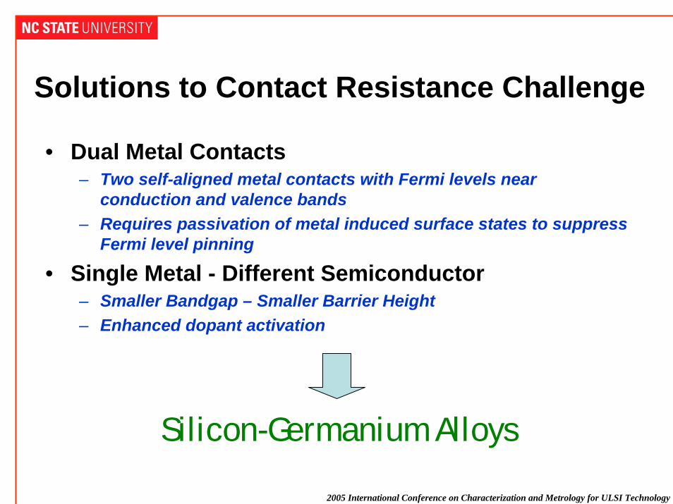
Solutions to Contact Resistance Challenge
• Dual Metal Contacts– Two self-aligned metal contacts with Fermi levels near
conduction and valence bands– Requires passivation of metal induced surface states to suppress
Fermi level pinning
• Single Metal - Different Semiconductor– Smaller Bandgap – Smaller Barrier Height– Enhanced dopant activation
Silicon-Germanium Alloys

2005 International Conference on Characterization and Metrology for ULSI Technology
SiGe Source/Drain Technology
• Form extension junction• Form sidewall spacer• Recess Source/Drain by RIE• Deposit In-Situ doped SiGe
NCSU-Motorola, 2002NCSU - IEDM 2000
2005 International Conference on Characterization and Metrology for ULSI Technology
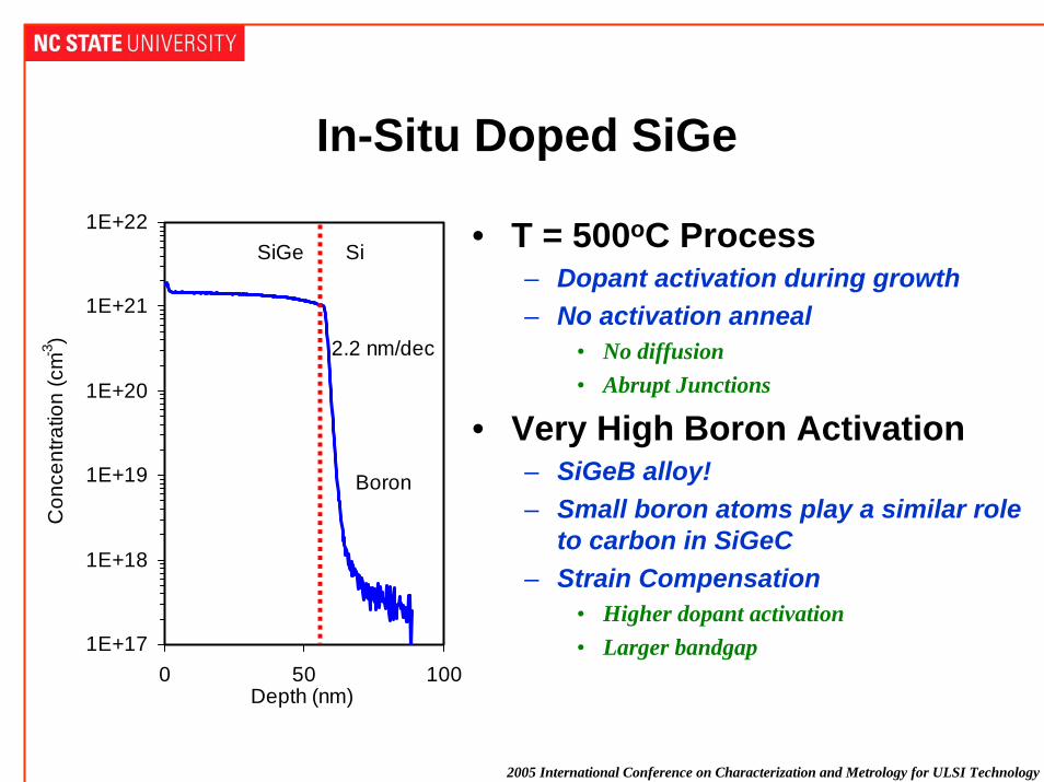
In-Situ Doped SiGe
1E+17
1E+18
1E+19
1E+20
1E+21
1E+22
0 50 100Depth (nm)
Con
cent
ratio
n (c
m-3)
Boron
SiGe Si
2.2 nm/dec
• T = 500oC Process– Dopant activation during growth– No activation anneal
• No diffusion• Abrupt Junctions
• Very High Boron Activation– SiGeB alloy!– Small boron atoms play a similar role
to carbon in SiGeC– Strain Compensation
• Higher dopant activation• Larger bandgap

2005 International Conference on Characterization and Metrology for ULSI Technology
Boron Activation in SiGe
1E+19
1E+20
1E+21
1E+22
1E-06 1E-05 1E-04 1E-03 1E-02B2H6 Partial Pressure (Torr)
Dop
ing
Con
cent
ratio
n (c
m-3
)
From SIMS
p + Si
p + Si 0.4Ge 0.6
From Hall NCSU 2001
1E-4
1E-3
1E-2
1E-06 1E-05 0.0001 0.001 0.01B2H6 Partial Pressure (Torr)
Res
istiv
ity (O
hm-c
m)
p +Si
p +Si 0.4Ge 0.6

2005 International Conference on Characterization and Metrology for ULSI Technology
Nickel Germanosilicide Contacts to SiGe
0
20
40
60
80
100
200 400 600 800 1000RTA Temperature (°C)
She
et R
esis
tanc
e (o
hms/
sq)
As Deposited
Undoped SiGe
p+ SiGe10 nm 20 nm
10 nm
20 nm
0
100
200
300
400
500
600
700
32 34 36 38 40 42 44 46 482 theta
Cou
nts
(102) (112) (211)
(210)
NiSi
400ºC
500ºC
600ºC
700ºC
800ºC
350ºC
Si(200)
• Above 400oC, Ge atoms– Leave the germanosilicide grains and segregate at the grain boundaries
• Reason:– A large difference in the silicide and germanosilicide heat of formation
2005 International Conference on Characterization and Metrology for ULSI Technology
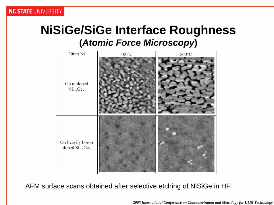
NiSiGe/SiGe Interface Roughness(Atomic Force Microscopy)
AFM surface scans obtained after selective etching of NiSiGe in HF
2005 International Conference on Characterization and Metrology for ULSI Technology
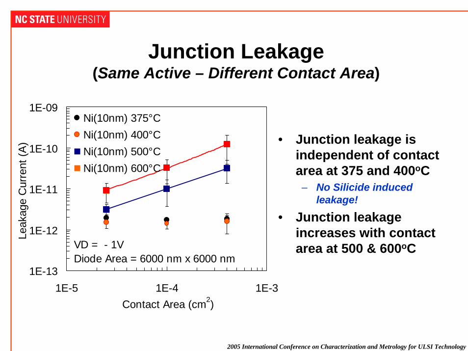
Junction Leakage(Same Active – Different Contact Area)
1E-13
1E-12
1E-11
1E-10
1E-09
1E-5 1E-4 1E-3Contact Area (cm2)
Leak
age
Cur
rent
(A)
Ni(10nm) 375°CNi(10nm) 400°CNi(10nm) 500°CNi(10nm) 600°C
VD = - 1VDiode Area = 6000 nm x 6000 nm
• Junction leakage is independent of contact area at 375 and 400oC
– No Silicide induced leakage!
• Junction leakage increases with contact area at 500 & 600oC

2005 International Conference on Characterization and Metrology for ULSI Technology
Si-SiGe Interface After Selective Etching of Germanosilicide and SiGe
With the loss of Ge from the germanosilicide grains, Ni diffusion into the underlying SiGe results in NiSi spikes that extend deep into the substrate
1E+0
1E+1
1E+2
1E+3
1E+4
1E+5
1E+6
1E+7
0 200 400 600 800
Time
Cou
nts
Ni
Si
Ge
B
450°C
1E+0
1E+1
1E+2
1E+3
1E+4
1E+5
1E+6
1E+7
0 200 400 600 800
Time
Cou
nts
Ni
Si
B
Ge
500°C

2005 International Conference on Characterization and Metrology for ULSI Technology
Ni/Pt Germanosilicide
0
10
20
30
40
50
60
70
80
90
100
200 300 400 500 600 700 800Temperature (oC)
Shee
t Res
ista
nce
(Ohm
s/sq
.)As Deposited
p+SiGe
Undoped SiGe
0
10
20
30
40
50
60
70
80
90
100
200 300 400 500 600 700 800
Temperature (oC)
Shee
t Res
ista
nce
(Ohm
s/sq
.)
As Deposited
p+SiGe
Undoped SiGe
Ni(10nm) Ni(10nm)/Pt(1nm) Ni(7.5nm)/Pt(2.5nm)
0
10
20
30
40
50
60
70
80
90
100
200 300 400 500 600 700 800Temperature (ºC)
Shee
t Res
ista
nce
(Ohm
/sq.
)
As Deposited
p+SiGe
Undoped SiGe
SiGe
Ni (10 nm) Pt (1 nm)
Sheet resistance thermal stability greatly improvedOn p+ SiGe - sheet resistance of Ni(7.5nm)/Pt(2.5nm) is stable up to 700ºC

2005 International Conference on Characterization and Metrology for ULSI Technology
Ni/Pt Germanosilicide Interface
1E+00
1E+01
1E+02
1E+03
1E+04
1E+05
1E+06
1E+07
0 200 400 600 800
Sputtering Time (sec)
Cou
nts
BSiNiGePt
Ni(10nm)/Pt(1nm)
RMS Interface Roughness ~ 1 nm
2005 International Conference on Characterization and Metrology for ULSI Technology
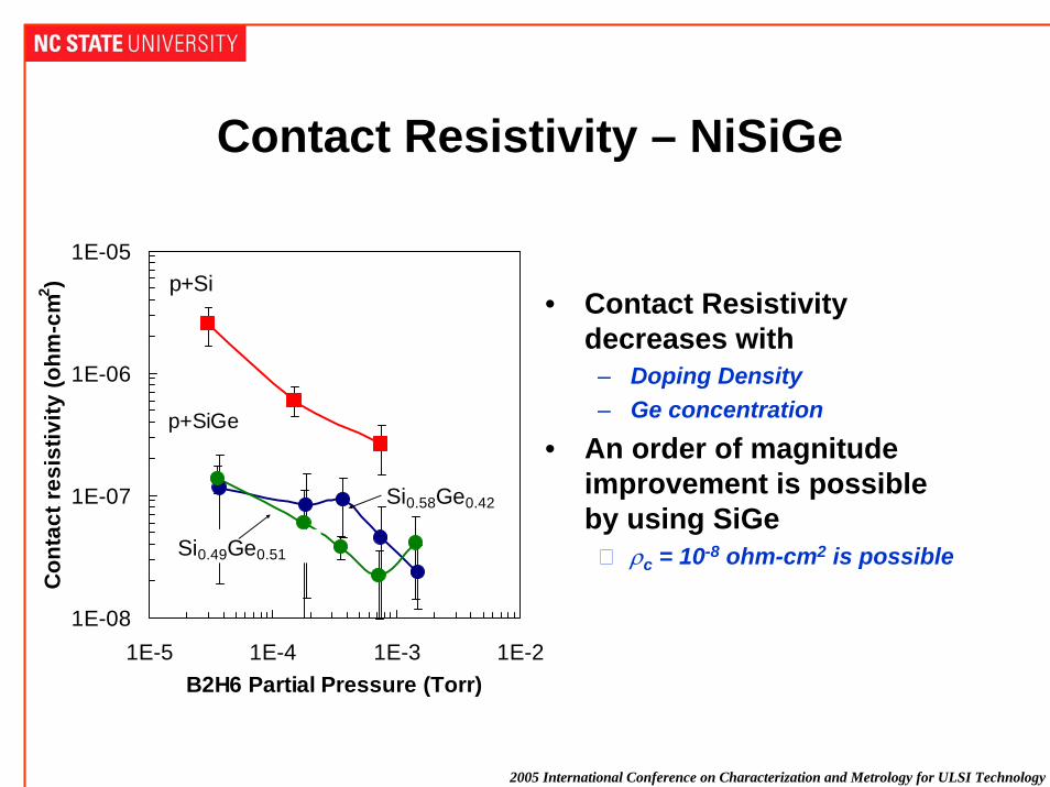
Contact Resistivity – NiSiGe
1E-08
1E-07
1E-06
1E-05
1E-5 1E-4 1E-3 1E-2B2H6 Partial Pressure (Torr)
Con
tact
resi
stiv
ity (o
hm-c
m2 )
Si0.58Ge0.42
Si0.49Ge0.51
p+Si
p+SiGe
• Contact Resistivity decreases with
– Doping Density– Ge concentration
• An order of magnitude improvement is possible by using SiGe
ρc = 10-8 ohm-cm2 is possible
2005 International Conference on Characterization and Metrology for ULSI Technology
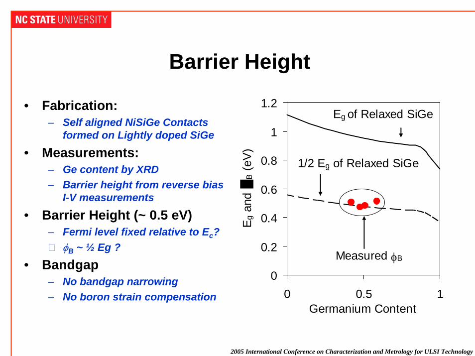
Barrier Height
0
0.2
0.4
0.6
0.8
1
1.2
0 0.5 1Germanium Content
Eg
and
B (e
V)
Eg of Relaxed SiGe
1/2 Eg of Relaxed SiGe
Measured φB
• Fabrication:– Self aligned NiSiGe Contacts
formed on Lightly doped SiGe
• Measurements:– Ge content by XRD– Barrier height from reverse bias
I-V measurements
• Barrier Height (~ 0.5 eV)– Fermi level fixed relative to Ec?
φB ~ ½ Eg ?
• Bandgap– No bandgap narrowing– No boron strain compensation
2005 International Conference on Characterization and Metrology for ULSI Technology
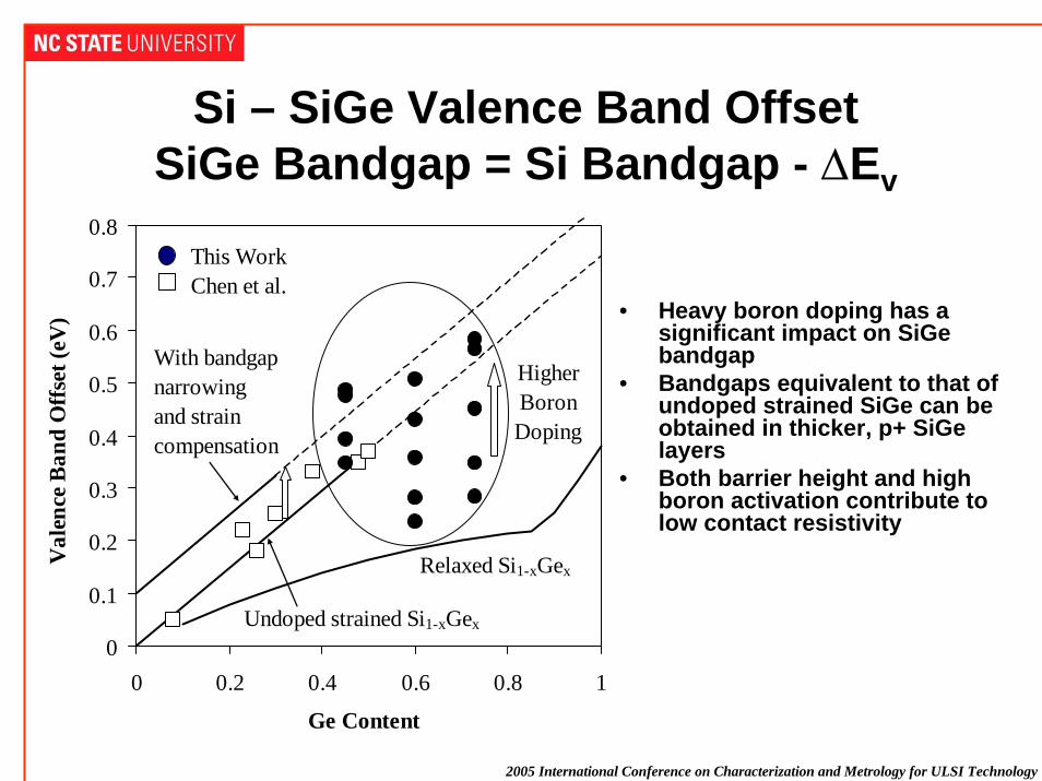
Si – SiGe Valence Band OffsetSiGe Bandgap = Si Bandgap - ∆Ev
• Heavy boron doping has a significant impact on SiGe bandgap
• Bandgaps equivalent to that of undoped strained SiGe can be obtained in thicker, p+ SiGe layers
• Both barrier height and high boron activation contribute to low contact resistivity
0
0.1
0.2
0.3
0.4
0.5
0.6
0.7
0.8
0 0.2 0.4 0.6 0.8 1
Ge Content
Val
ence
Ban
d O
ffse
t (eV
)
With bandgap narrowing and strain compensation
Relaxed Si1-xGex
Undoped strained Si1-xGex
HigherBoronDoping
This Work Chen et al.

2005 International Conference on Characterization and Metrology for ULSI Technology
Enhanced PMOS Mobility byLocal Strain - Source/Drain Engineering
2005 International Conference on Characterization and Metrology for ULSI Technology
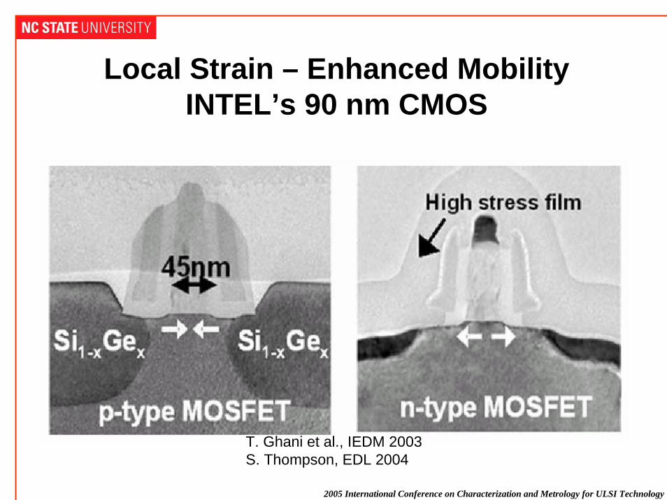
Local Strain – Enhanced MobilityINTEL’s 90 nm CMOS
T. Ghani et al., IEDM 2003S. Thompson, EDL 2004
2005 International Conference on Characterization and Metrology for ULSI Technology
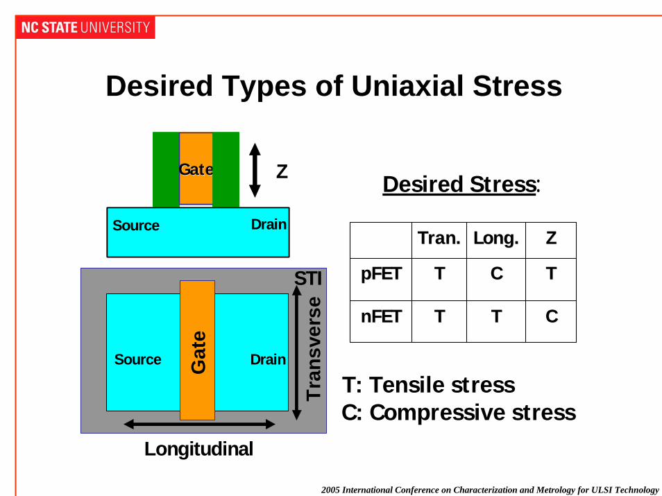
Desired Types of Uniaxial Stress
GateGate
Source Drain
GateGateGateGate
Source Drain
STI
Source DrainGat
e
Longitudinal
Tran
sver
se
Z
CCTTTTnFETnFET
TTCCTTpFETpFET
ZZLong.Long.Tran.Tran.
CCTTTTnFETnFET
TTCCTTpFETpFET
ZZLong.Long.Tran.Tran.
Desired Stress:
T: Tensile stressC: Compressive stress

2005 International Conference on Characterization and Metrology for ULSI Technology
PMOS Mobility
INTEL - August 2004
65 nm transistors exhibit 10-15% increase in drive current with enhanced strain

2005 International Conference on Characterization and Metrology for ULSI Technology
Fully-Depleted MOSFET Structures
2005 International Conference on Characterization and Metrology for ULSI Technology
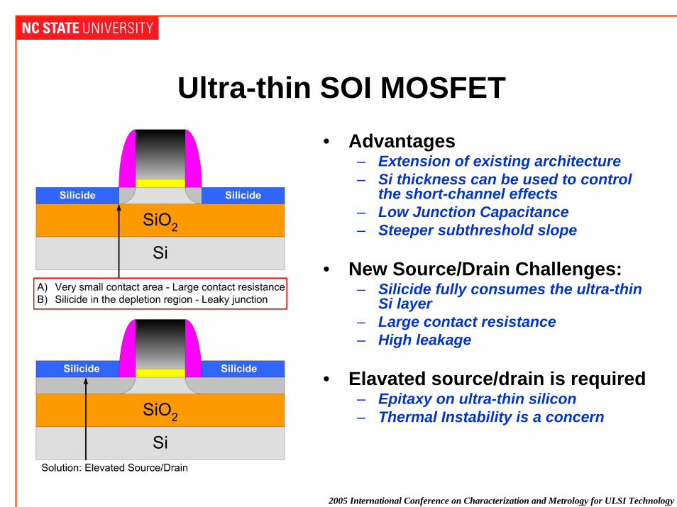
Ultra-thin SOI MOSFET• Advantages
– Extension of existing architecture– Si thickness can be used to control
the short-channel effects– Low Junction Capacitance– Steeper subthreshold slope
• New Source/Drain Challenges:– Silicide fully consumes the ultra-thin
Si layer– Large contact resistance– High leakage
• Elavated source/drain is required– Epitaxy on ultra-thin silicon– Thermal Instability is a concern

2005 International Conference on Characterization and Metrology for ULSI Technology
Strained Silicon Directly on Insulator• Similar to Ultra-thin SOI• Enhanced Mobility• Strained Silicon w/o SiGe
– Ge diffusion into Si is not an issue– Integration is simpler

2005 International Conference on Characterization and Metrology for ULSI Technology
SSDOI Mobility– IBM
(a)(a) (b)(b) (c)(c)(a)(a) (b)(b) (c)(c)
2003

2005 International Conference on Characterization and Metrology for ULSI Technology
FINFET
• Promising future!• 3-D Silicon on Insulator Technology• Fully-Depleted, Double Gate MOSFET

2005 International Conference on Characterization and Metrology for ULSI Technology
FINFET Source/Drain Engineering
• Extension Resistance:– Narrow fin - large resistance under
the spacer– Similar to ultra-thin SOI
• Contact Resistance– Silicide should not be allowed to
consume the fin– The fin should be expanded in all
three directions– Novel contacting solutions will still
be necessary for low contact resistance
• SiGe epi instead of Si• Dual metal contacts
2005 International Conference on Characterization and Metrology for ULSI Technology
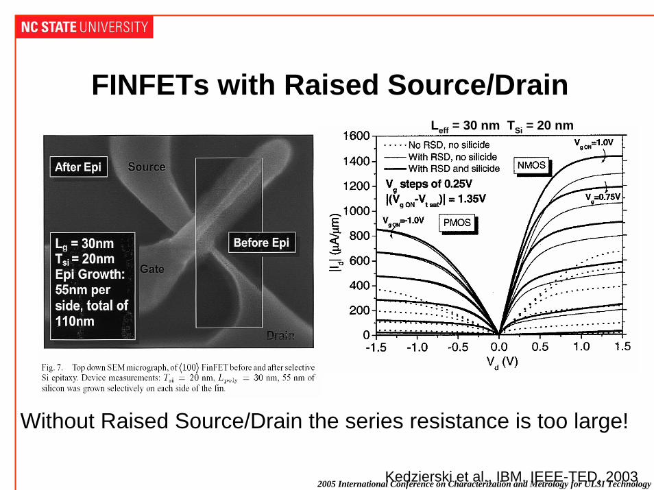
FINFETs with Raised Source/DrainLeff = 30 nm TSi = 20 nm
Without Raised Source/Drain the series resistance is too large!
Kedzierski et al., IBM, IEEE-TED, 2003

2005 International Conference on Characterization and Metrology for ULSI Technology
Summary
• Parasitic series resistance is a grand challenge for future CMOS generations– Contact and Overlap Resistances are the key contributors
• Silicon-Germanium Source/Drain Technology can provide:– Local Strain for Enhanced Mobility– High boron activation and small barrier height for low-contact
resistivity– Low-temperature processing for compatibility with high-k
dielectrics and metal gate electrodes– Abrupt Junctions for small overlap resistance– Elevated source/drain for fully depleted MOSFETs with ultra-thin
Si channels


![Paul Scherrer Institute Evaluation of resist performance ...40 45 20 25 30 35 40 45 ] Dose [mJ/cm2] HP 16 nm HP 18 nm HP 20 nm HP 22 nm HP 30 nm Thickness=30 nm °C / 60 s PEB: 100](https://img.pdfslide.us/doc/110x75/606f7cd001284100010f52e4/paul-scherrer-institute-evaluation-of-resist-performance-40-45-20-25-30-35-40.jpg)