Embed Size (px)
Citation preview
LOW-TERAHERTZ TRANSMISSIVITY
WITH A GRAPHENE-DIELECTRIC
MICRO-STRUCTURE
Chandra S. R. Kaipa, Alexander B. Yakovlev
George W. Hanson, Yashwanth R. Padooru
Francisco Medina, Francisco Mesa
IEEE MTT-S International Microwave Symposium
Montréal, Québec, Canada, 17-22 June 2012
TU2D: Applications of Carbon-Based RF Technology
Introduction and Motivation
Graphene-Dielectric Stack
Results and Discussions
Conclusions
2
OUTLINE
Enhanced Transmission at low-THz
Broadband Filters
Frequency of Enhanced Transmission (Excess Length
Concept)

3
Extremely thin conducting layers are almost opaque.
However, multilayer metal-dielectric PBG-like structures become
transparent within certain frequency bands in the optical regime.
I. R. Hooper et al., Opt. Express, 16, 17249 (2008)
M. R. Gadsdon et al., J. Opt. Soc. Am. B, 26, 734 (2009)
Induced transparency in the optical regime
BACKGROUND AND MOTIVATION (1)
4
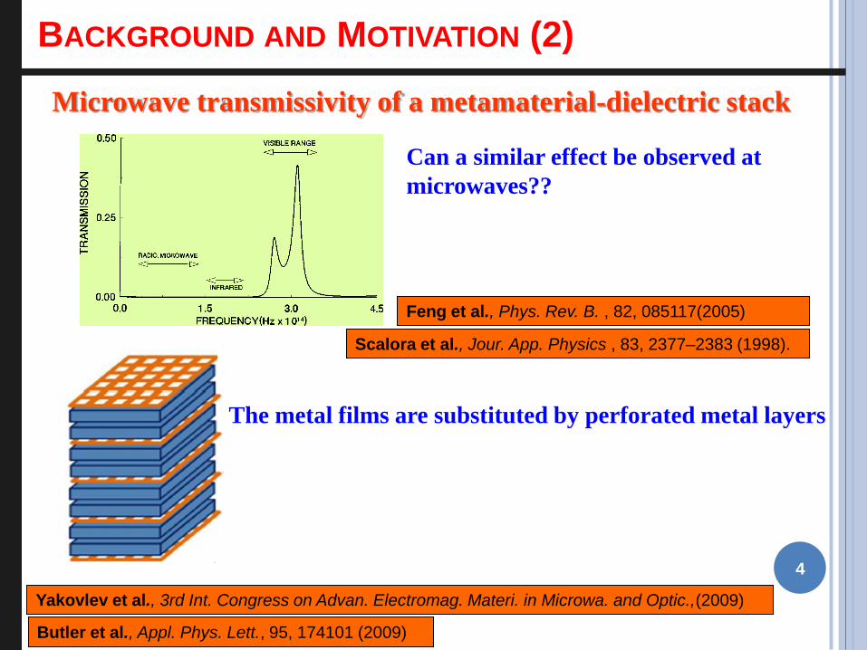
Can a similar effect be observed at
microwaves??
The metal films are substituted by perforated metal layers
Microwave transmissivity of a metamaterial-dielectric stack
Butler et al., Appl. Phys. Lett., 95, 174101 (2009)
Yakovlev et al., 3rd Int. Congress on Advan. Electromag. Materi. in Microwa. and Optic.,(2009)
BACKGROUND AND MOTIVATION (2)
Scalora et al., Jour. App. Physics , 83, 2377–2383 (1998).
Feng et al., Phys. Rev. B. , 82, 085117(2005)
5 6 7 8 9 10 11 12 13 14 15 160
0.2
0.4
0.6
0.8
11
Frequency (GHz)
|S21|2
|S21|2 FEM model
|S21|2 Experimental
|S21|2 Analytical
A
B C D
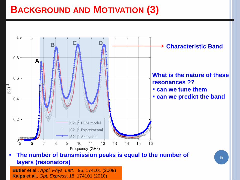
BACKGROUND AND MOTIVATION (3)
Characteristic Band
What is the nature of these
resonances ??
can we tune them
can we predict the band
The number of transmission peaks is equal to the number of
layers (resonators) 5
Butler et al., Appl. Phys. Lett. , 95, 174101 (2009)
Kaipa et al., Opt. Express, 18, 174101 (2010)
6
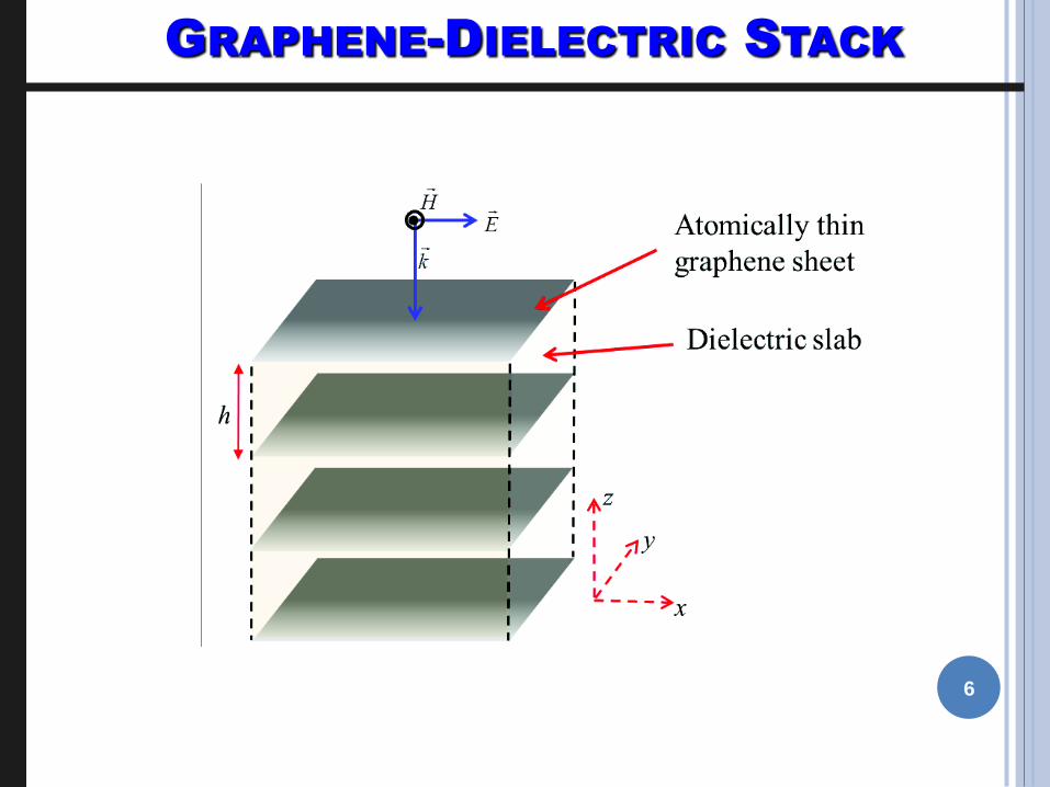
GRAPHENE-DIELECTRIC STACK
7
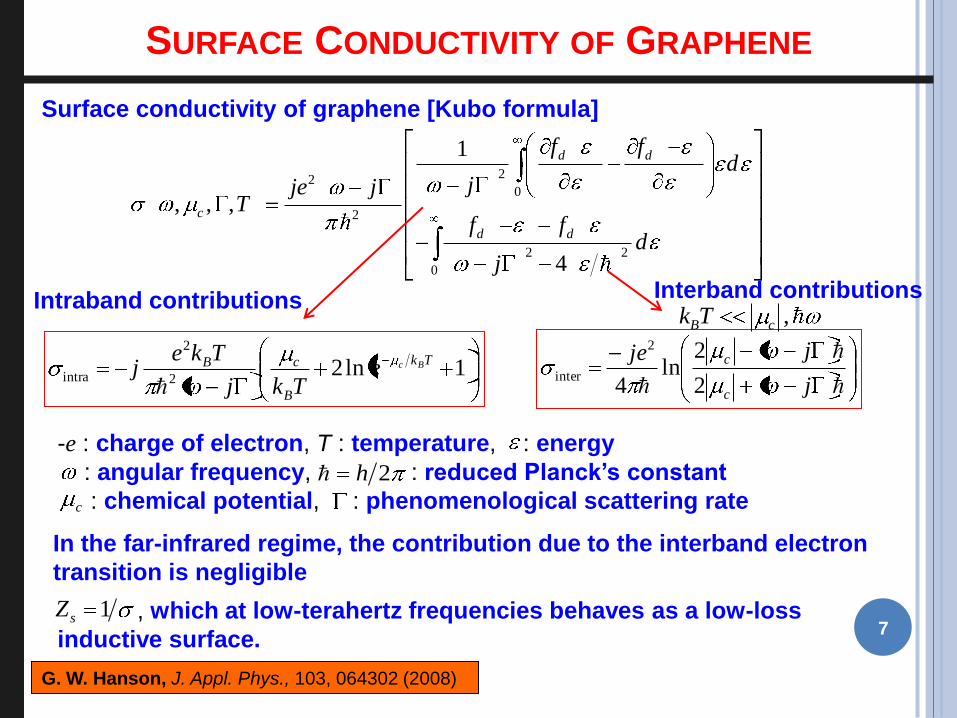
SURFACE CONDUCTIVITY OF GRAPHENE
220
2
2 2
0
1
, , ,
4
d d
c
d d
f fd
jje jT
f fd
j
Surface conductivity of graphene [Kubo formula]
, which at low-terahertz frequencies behaves as a low-loss
inductive surface.
1sZ
G. W. Hanson, J. Appl. Phys., 103, 064302 (2008)
1ln22
2
intra
Tk
B
cB BceTkj
Tkej
j
jje
c
c
2
2ln
4
2
inter
Intraband contributions Interband contributions
-e : charge of electron, T : temperature, : energy
: angular frequency, : reduced Planck’s constant
: chemical potential, : phenomenological scattering rate
2hc
In the far-infrared regime, the contribution due to the interband electron
transition is negligible
,B ck T

8
Solid lines: approximate closed-form expressions (intraband + interband)
Dashed lines: numerical integration [Kubo formula]
SURFACE CONDUCTIVITY GRAPHENE
2 5
min
1/ 1.32 meV, 0.5 ps, 300 K
/ 2 6.085 10 S
T
e h
0.2 eVc 0.5 eVc
1 3 5 7 9 11 13 150
50
100
150
Frequency [THz]
Co
nductiv
ity
Re ( /min
)
Im ( /min
)
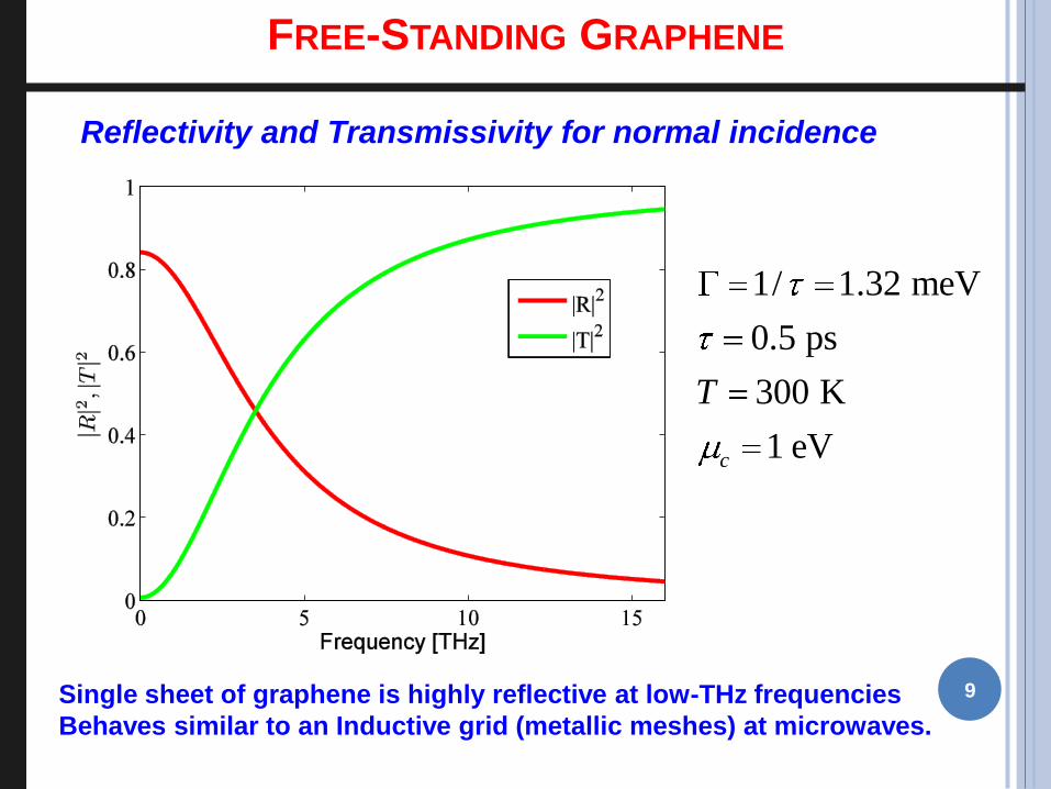
9 Single sheet of graphene is highly reflective at low-THz frequencies
Behaves similar to an Inductive grid (metallic meshes) at microwaves.
Reflectivity and Transmissivity for normal incidence
FREE-STANDING GRAPHENE
1/ 1.32 meV
0.5 ps
300 K
1 eVc
T
10
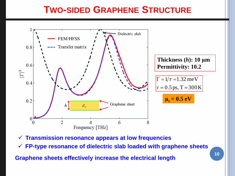
TWO-SIDED GRAPHENE STRUCTURE
Thickness (h): 10 μm
Permittivity: 10.2
K 300 T ps, 0.5
meV 23.11
Transmission resonance appears at low frequencies
Graphene sheets effectively increase the electrical length
FP-type resonance of dielectric slab loaded with graphene sheets
μc = 0.5 eV
11
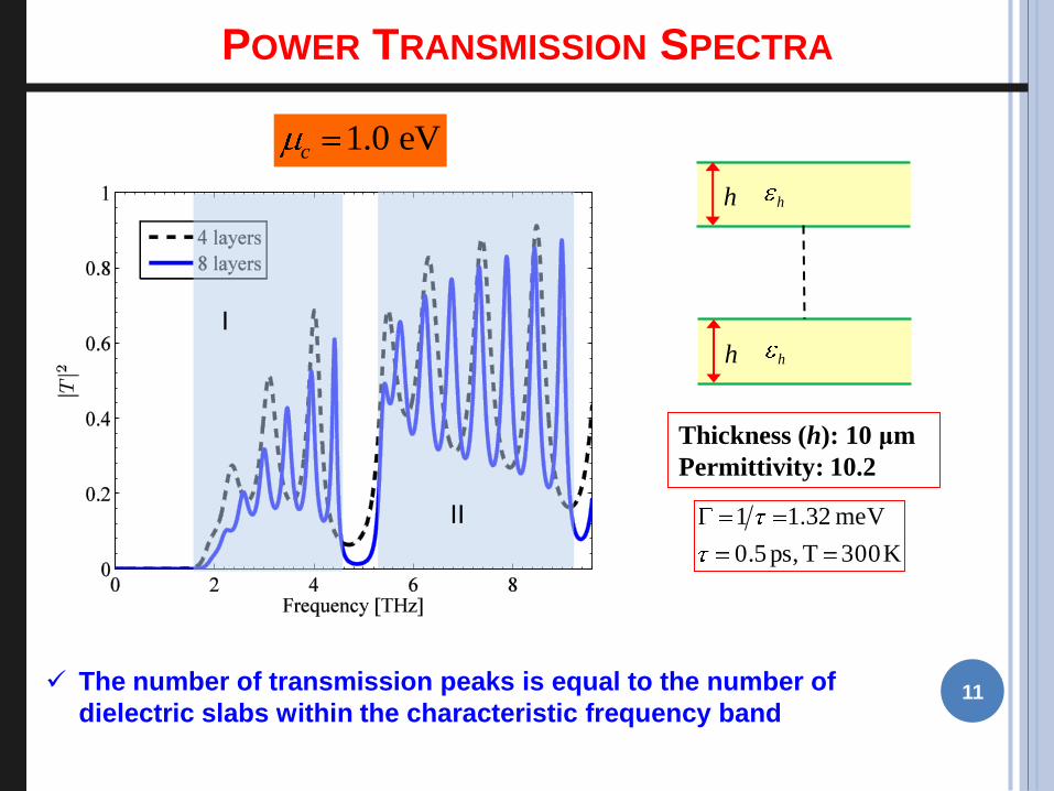
POWER TRANSMISSION SPECTRA
The number of transmission peaks is equal to the number of
dielectric slabs within the characteristic frequency band
Thickness (h): 10 μm
Permittivity: 10.2
K 300 T ps, 0.5
meV 23.11
h h
h h
1.0 eVc
I
II

12
POWER TRANSMISSION SPECTRA
Enhanced transmission at low-THz
Fabry-Perot resonances of the individual open/coupled cavities
Thickness (h): 10 μm
Permittivity: 10.2
K 300 T ps, 0.5
meV 23.11
4 layer graphene structure
- 4 dielectric slabs
- 5 graphene sheets
h h
h h
A
B C
D
13
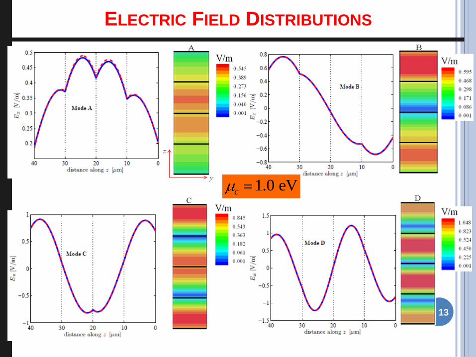
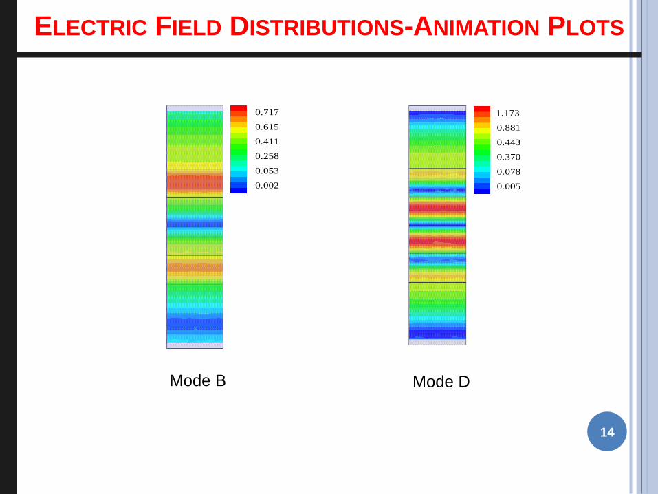
ELECTRIC FIELD DISTRIBUTIONS
1.0 eVc
14
ELECTRIC FIELD DISTRIBUTIONS-ANIMATION PLOTS
0.005
0.078
0.370
0.443
0.881
1.173
Mode D
0.002
0.053
0.258
0.411
0.615
0.717
Mode B
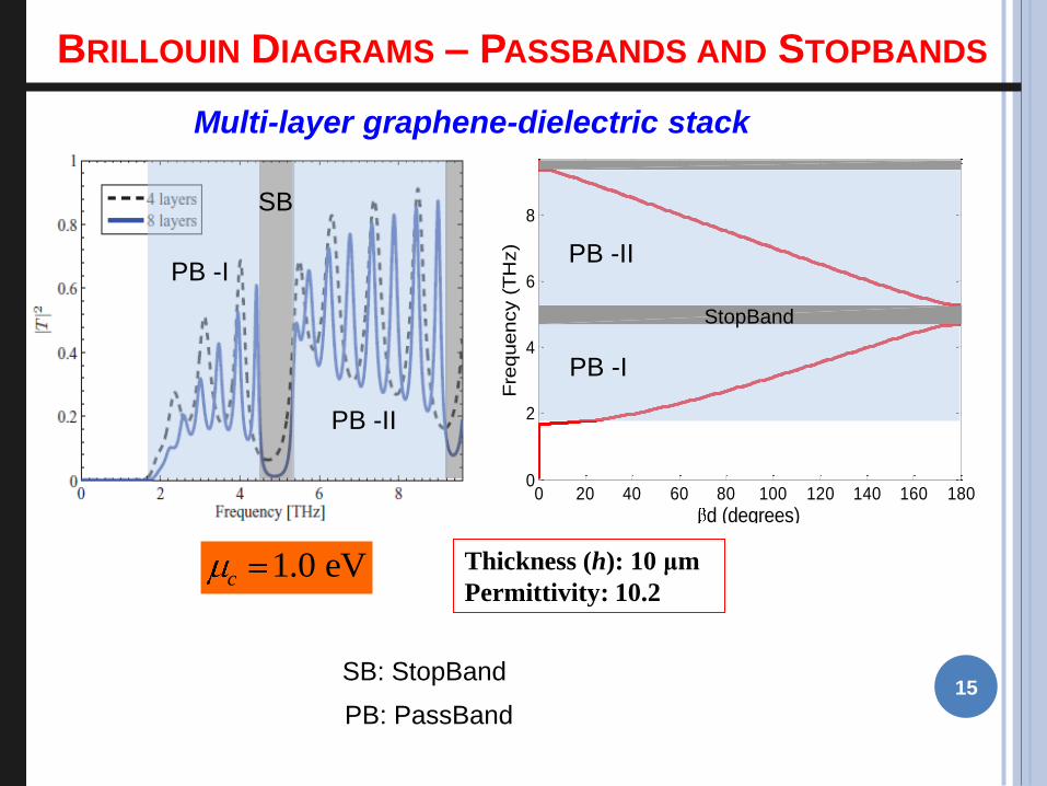
0 20 40 60 80 100 120 140 160 1800
2
4
6
8
d (degrees)F
requency (
TH
z)
15
PB -I
SB
PB -II
PB -I
PB -II
BRILLOUIN DIAGRAMS – PASSBANDS AND STOPBANDS
Thickness (h): 10 μm
Permittivity: 10.2 1.0 eVc
StopBand
Multi-layer graphene-dielectric stack
SB: StopBand
PB: PassBand
0 20 40 60 80 100 120 140 160 1803.5
4
4.5
5
5.5
6
6.5
d (degrees)F
requency (
TH
z)
16
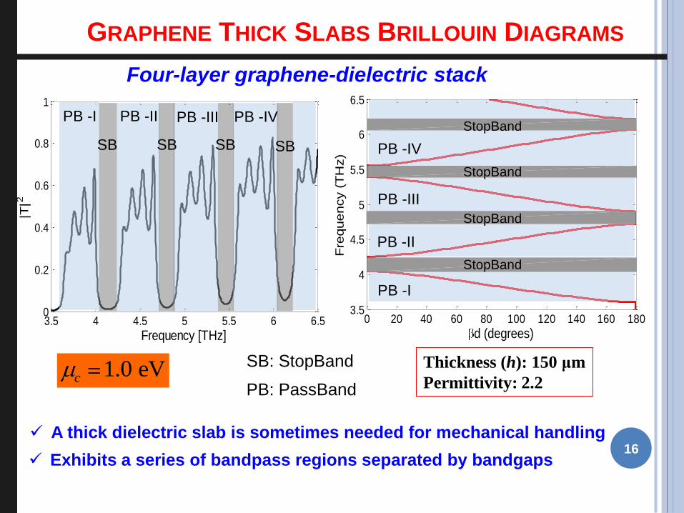
Thickness (h): 150 μm
Permittivity: 2.2 1.0 eVc
3.5 4 4.5 5 5.5 6 6.50
0.2
0.4
0.6
0.8
1
Frequency [THz]
|T|2
PB -I
PB -II
PB -III
PB -IV
PB -I PB -II PB -III PB -IV
SB SB SB SB
GRAPHENE THICK SLABS BRILLOUIN DIAGRAMS
StopBand
StopBand
StopBand
StopBand
Four-layer graphene-dielectric stack
SB: StopBand
PB: PassBand
Exhibits a series of bandpass regions separated by bandgaps
A thick dielectric slab is sometimes needed for mechanical handling
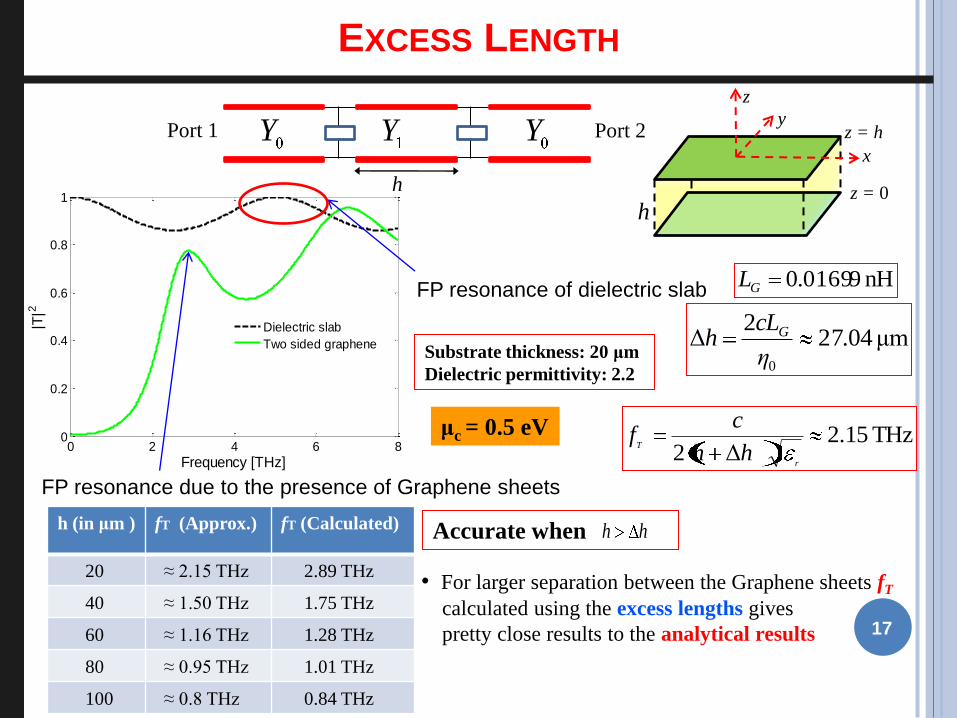
0 2 4 6 80
0.2
0.4
0.6
0.8
1
Frequency [THz]
|T|2
Dielectric slab
Two sided graphene
nH 90169.0GL
h
x
z
y z = h
z = 0
Substrate thickness: 20 μm
Dielectric permittivity: 2.2
FP resonance of dielectric slab
FP resonance due to the presence of Graphene sheets
μm 40.272
Δ0η
cLh G
THz 15.2Δ2
r
T
hh
cf
Accurate when hh
EXCESS LENGTH
17
h (in μm ) fT (Approx.) fT (Calculated)
20 ≈ 2.15 THz 2.89 THz
40 ≈ 1.50 THz 1.75 THz
60 ≈ 1.16 THz 1.28 THz
80 ≈ 0.95 THz 1.01 THz
100 ≈ 0.8 THz 0.84 THz
• For larger separation between the Graphene sheets fT
calculated using the excess lengths gives
pretty close results to the analytical results
μc = 0.5 eV
Y YY Port 2 Port 1
h
18
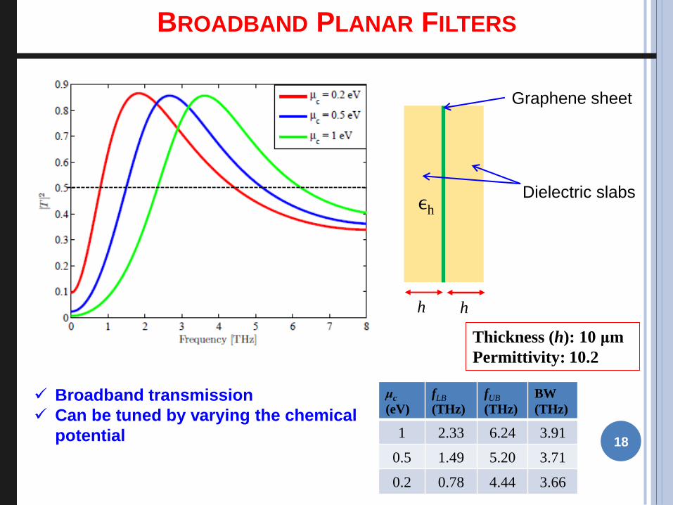
BROADBAND PLANAR FILTERS
μc
(eV)
fLB
(THz)
fUB
(THz)
BW
(THz)
1 2.33 6.24 3.91
0.5 1.49 5.20 3.71
0.2 0.78 4.44 3.66
Graphene sheet
Dielectric slabs
h
ϵh
h
Thickness (h): 10 μm
Permittivity: 10.2
Broadband transmission
Can be tuned by varying the chemical
potential
19
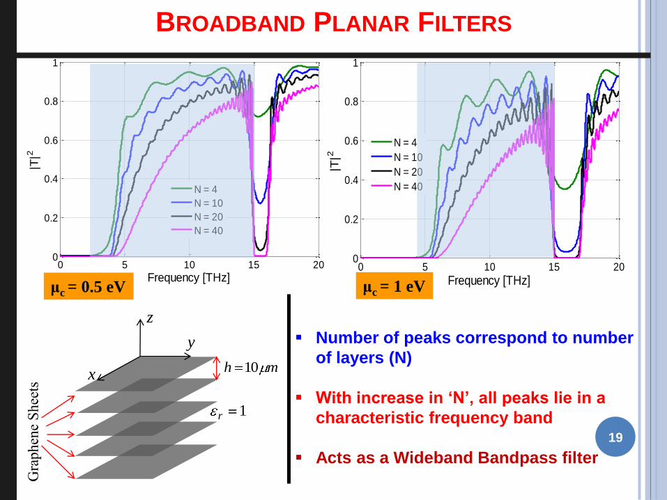
0 5 10 15 200
0.2
0.4
0.6
0.8
1
Frequency [THz]
|T|2
N = 4
N = 10
N = 20
N = 40
0 5 10 15 200
0.2
0.4
0.6
0.8
1
Frequency [THz]
|T|2
N = 4
N = 10
N = 20
N = 40
μc = 0.5 eV μc = 1 eV
1r
z
x
y
mh 10
Number of peaks correspond to number
of layers (N)
With increase in ‘N’, all peaks lie in a
characteristic frequency band
Acts as a Wideband Bandpass filter
BROADBAND PLANAR FILTERS
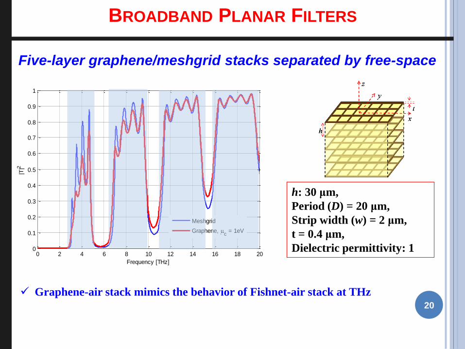
20
h: 30 μm,
Period (D) = 20 μm,
Strip width (w) = 2 μm,
t = 0.4 μm,
Dielectric permittivity: 1
Graphene-air stack mimics the behavior of Fishnet-air stack at THz
Five-layer graphene/meshgrid stacks separated by free-space
0 2 4 6 8 10 12 14 16 18 200
0.1
0.2
0.3
0.4
0.5
0.6
0.7
0.8
0.9
1
Frequency [THz]
|T|2
Meshgrid
Graphene, c = 1eV
BROADBAND PLANAR FILTERS
21
CONCLUSIONS
Tunable structures can be designed using stacked graphene sheets
We mimic the enhanced transmission at optical frequencies with a
metal-dielectric stack and in the microwave regime with stacked-
metascreens, at low-THz using stacked-graphene
The range of frequencies where the peaks are expected for a finite
graphene-dielectric stacked structure can be analytically and
accurately estimated from the Bloch analysis
Excess length concept has been successfully demonstrated
Broadband planar filters have been realized using a stack of graphene
sheets in free-space