Embed Size (px)
Citation preview
Challenges and Realities of Advanced Node Manufacturing Srinivasa R Banna PhD
Fellow & Director of Advanced Device Architecture
13 July 2016

Outline
• Motivation
• Pitch Scaling
–Fin, Gate, MOL & Metal
• Material Innovation
–Contacts
–Air gaps
–New channel materials
• New Device Architectures
–GAA
–Steep Subthreshold
• Summary
GLOBALFOUNDRIES 2
GLOBALFOUNDRIES 3
0.80
0.90
1.00
1.10
1.20
1.30
1.40
0.60 0.80 1.00 1.20 1.40
Aver
age
Frqu
ency
(a.u
)
Total Power (a.u)
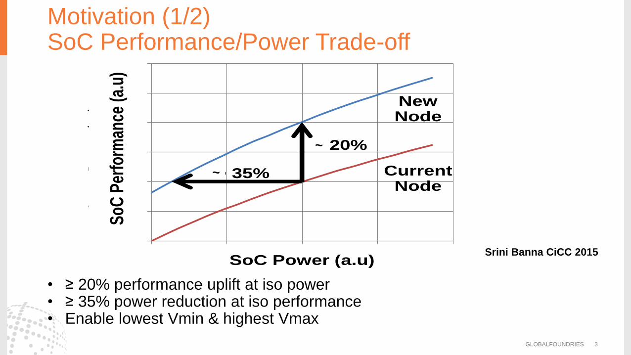
Current Node
New Node
> 20%
> 35%
SoC Power (a.u)
SoC
Per
form
ance
(a.
u)
• ≥ 20% performance uplift at iso power • ≥ 35% power reduction at iso performance • Enable lowest Vmin & highest Vmax
Motivation (1/2) SoC Performance/Power Trade-off
Srini Banna CiCC 2015
~
~
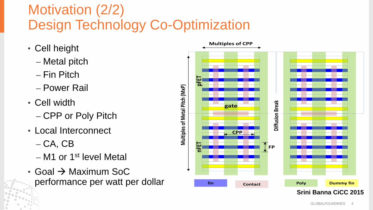
Motivation (2/2) Design Technology Co-Optimization
GLOBALFOUNDRIES 4
• Cell height
– Metal pitch
– Fin Pitch
– Power Rail
• Cell width
– CPP or Poly Pitch
• Local Interconnect
– CA, CB
– M1 or 1st level Metal
• Goal Maximum SoC performance per watt per dollar Poly Dummy finfin Contact
Multiples of CPP
Mul
tiple
s of M
etal
Pitc
h (M
xP)
FP
CPP
nFET
pFET
Diffu
sion
Brea
k
gate
Srini Banna CiCC 2015

Pitch Scaling
GLOBALFOUNDRIES 5
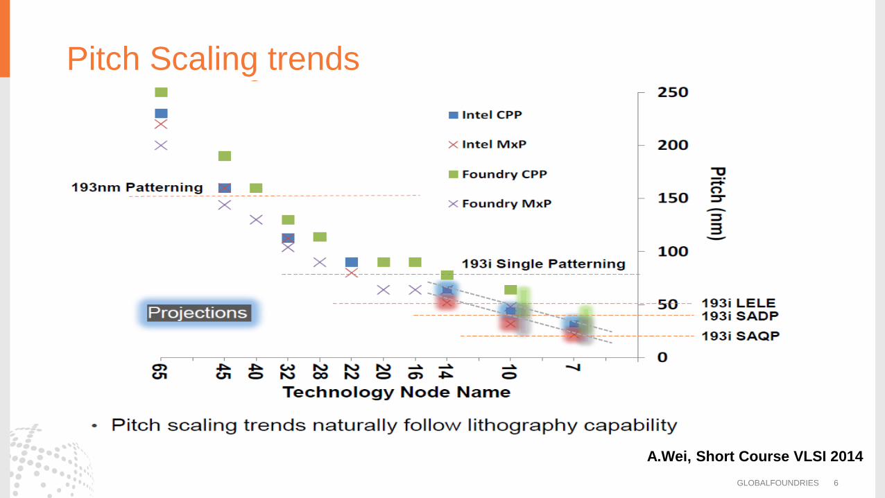
Pitch Scaling trends
GLOBALFOUNDRIES 6
A.Wei, Short Course VLSI 2014
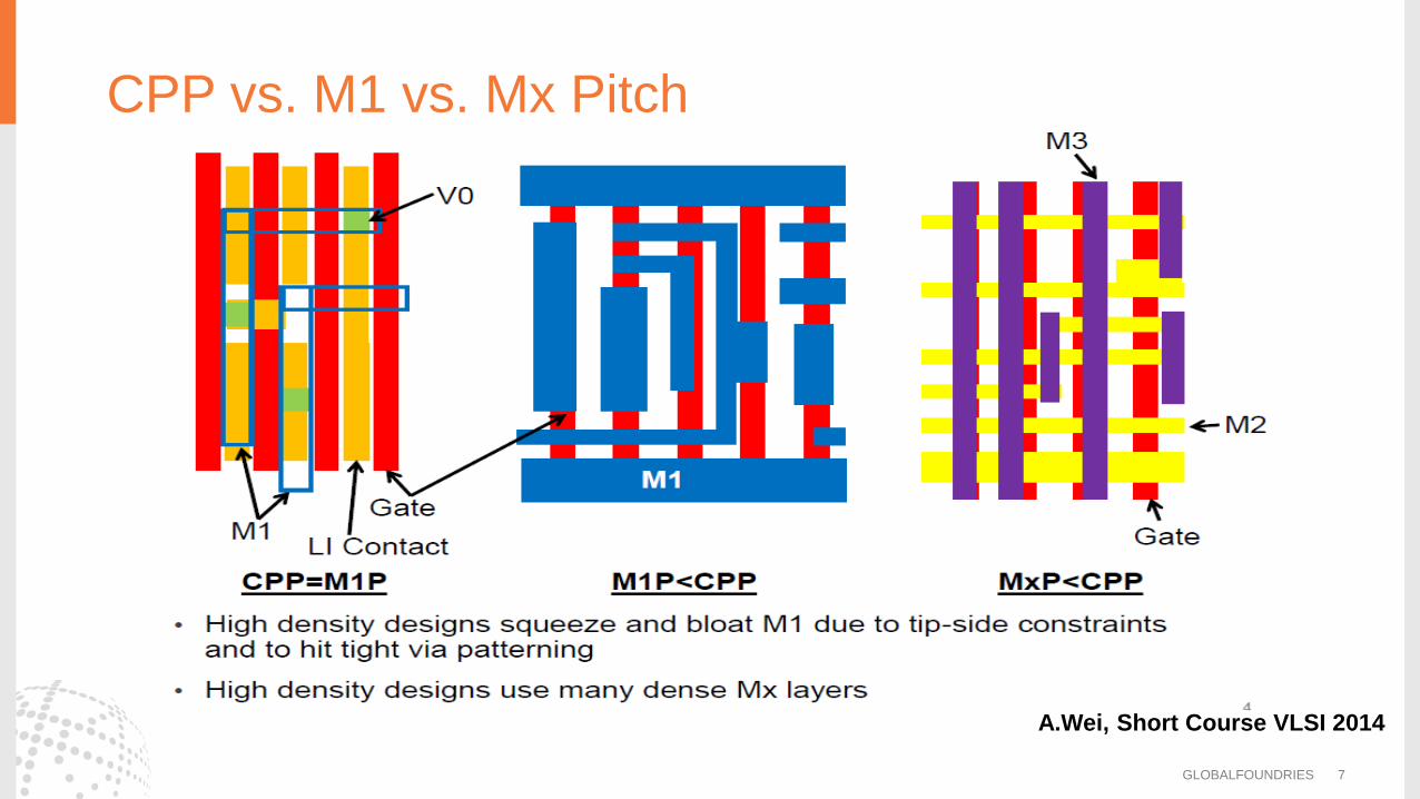
CPP vs. M1 vs. Mx Pitch
GLOBALFOUNDRIES 7
A.Wei, Short Course VLSI 2014
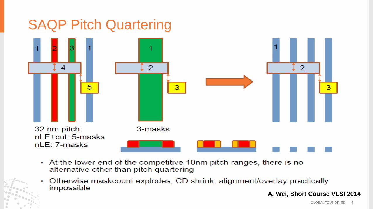
SAQP Pitch Quartering
GLOBALFOUNDRIES 8
A. Wei, Short Course VLSI 2014
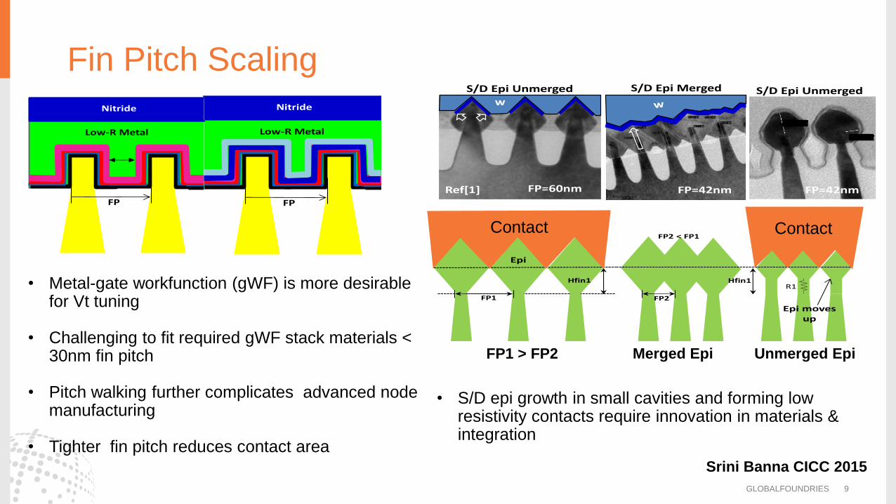
Fin Pitch Scaling
GLOBALFOUNDRIES 9
Nitride
Low-R Metal
FPPM
OS
Nitride
Low-R Metal
FP
NMO
S
S/D Epi MergedS/D Epi Unmerged
FP=42nmFP=60nm
wS/D Epi Unmerged
FP=42nmRef[1]
FP2
Hfin1
FP1
Hfin1
Epi moves up
Epi
R1
FP2 < FP1
Merged Epi Unmerged Epi FP1 > FP2
• Metal-gate workfunction (gWF) is more desirable for Vt tuning
• Challenging to fit required gWF stack materials < 30nm fin pitch
• Pitch walking further complicates advanced node
manufacturing
• Tighter fin pitch reduces contact area
• S/D epi growth in small cavities and forming low resistivity contacts require innovation in materials & integration
Contact Contact
Srini Banna CICC 2015
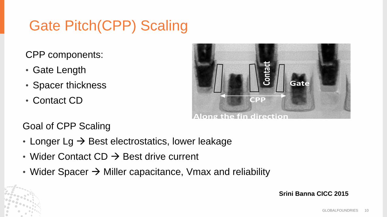
Gate Pitch(CPP) Scaling
GLOBALFOUNDRIES 10
CPP components:
• Gate Length
• Spacer thickness
• Contact CD
Goal of CPP Scaling
• Longer Lg Best electrostatics, lower leakage
• Wider Contact CD Best drive current
• Wider Spacer Miller capacitance, Vmax and reliability
Along the fin direction
CPP
Cont
act
Gate
Srini Banna CICC 2015
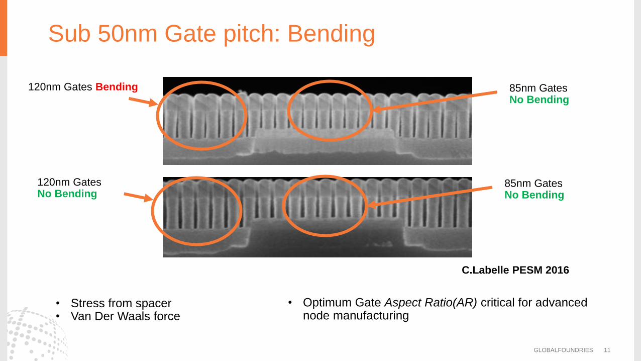
Sub 50nm Gate pitch: Bending
GLOBALFOUNDRIES 11
• Stress from spacer • Van Der Waals force
• Optimum Gate Aspect Ratio(AR) critical for advanced node manufacturing
120nm Gates Bending 85nm Gates No Bending
120nm Gates No Bending
85nm Gates No Bending
C.Labelle PESM 2016
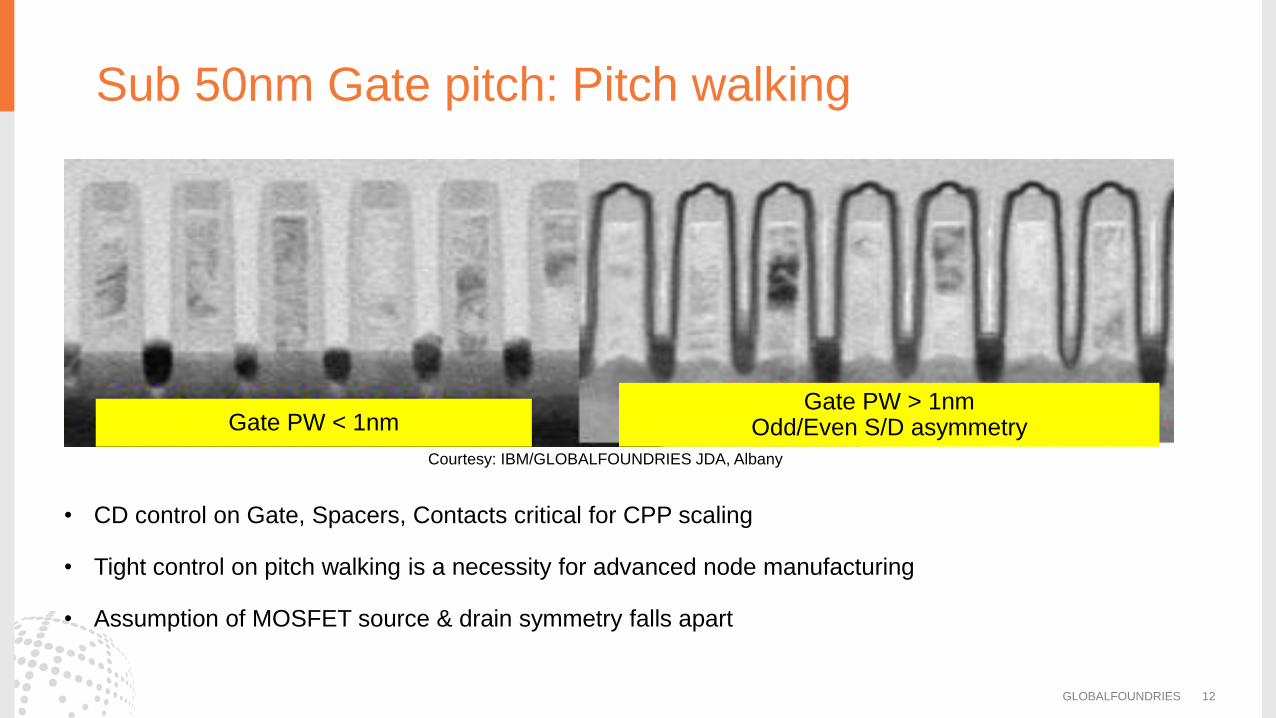
Sub 50nm Gate pitch: Pitch walking
GLOBALFOUNDRIES 12
Gate PW < 1nm Gate PW > 1nm
Odd/Even S/D asymmetry
• CD control on Gate, Spacers, Contacts critical for CPP scaling • Tight control on pitch walking is a necessity for advanced node manufacturing
• Assumption of MOSFET source & drain symmetry falls apart
Courtesy: IBM/GLOBALFOUNDRIES JDA, Albany
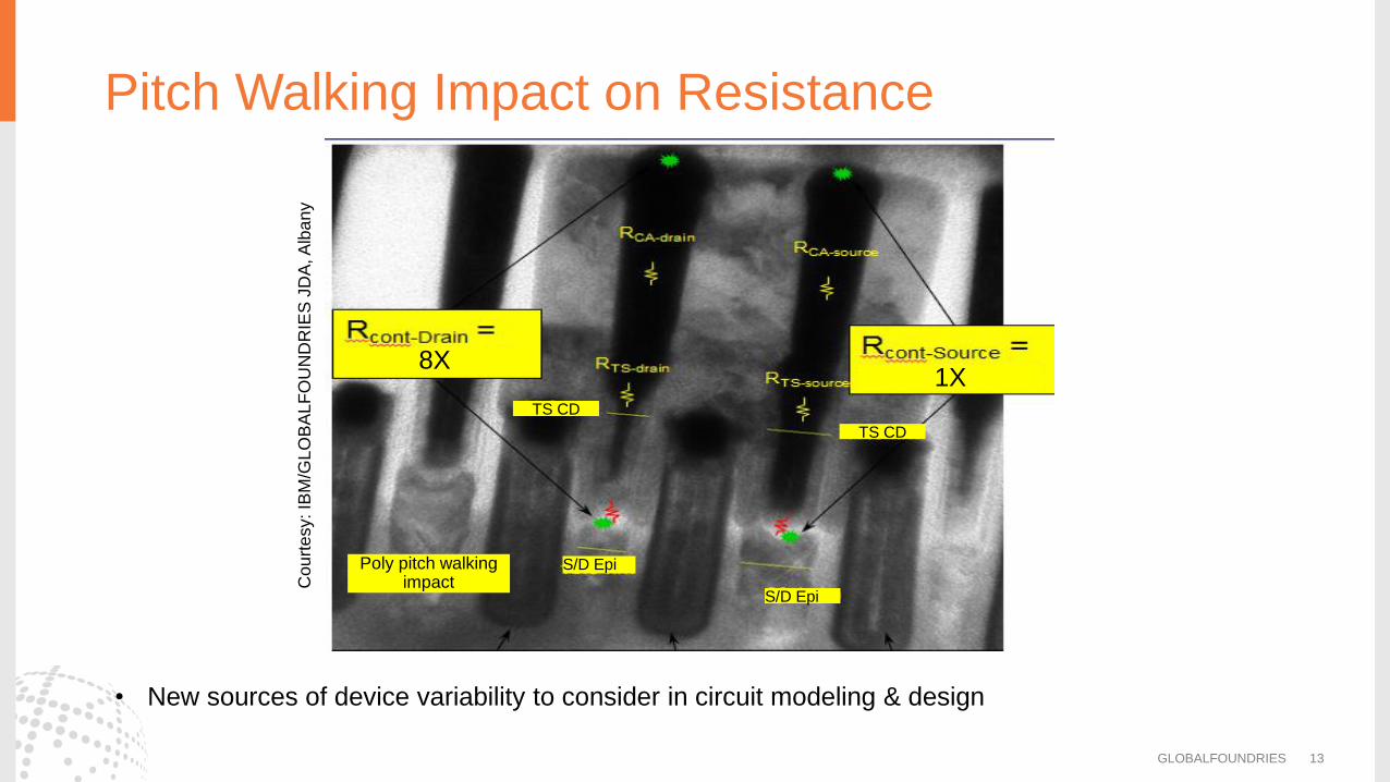
Pitch Walking Impact on Resistance
GLOBALFOUNDRIES 13
Poly pitch walking impact
S/D Epi
S/D Epi
TS CD
TS CD
• New sources of device variability to consider in circuit modeling & design
Cou
rtesy: IB
M/G
LO
BA
LF
OU
ND
RIE
S J
DA
, A
lba
ny
1X 8X
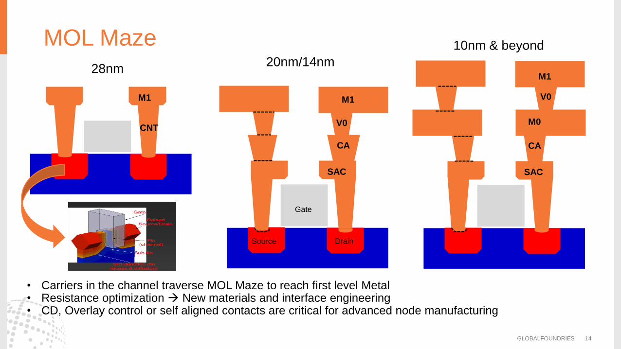
MOL Maze
GLOBALFOUNDRIES 14
SAC
M0
CA
V0
M1
SAC
CA
V0
M1 M1
CNT
28nm 20nm/14nm
10nm & beyond
• Carriers in the channel traverse MOL Maze to reach first level Metal • Resistance optimization New materials and interface engineering • CD, Overlay control or self aligned contacts are critical for advanced node manufacturing
Gate
Source Drain
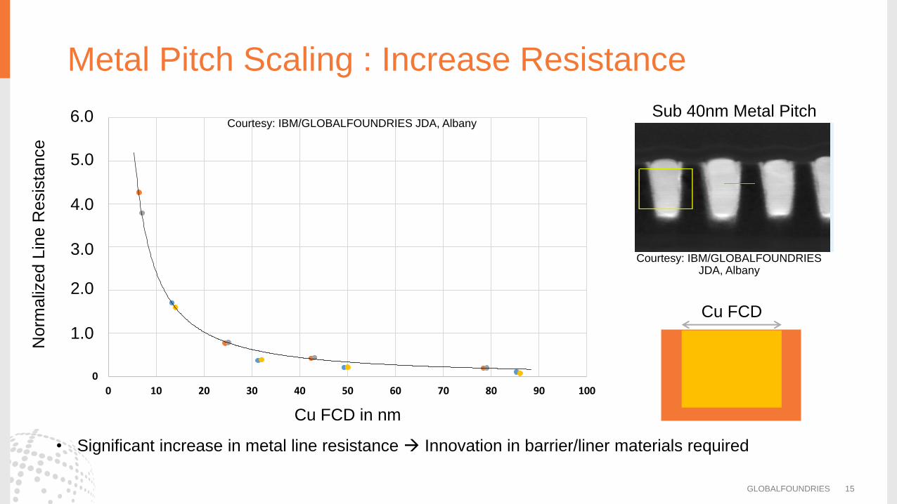
Metal Pitch Scaling : Increase Resistance
GLOBALFOUNDRIES 15
0
50
100
150
200
250
300
0 10 20 30 40 50 60 70 80 90 100
1.0
2.0
3.0
4.0
5.0
6.0 Sub 40nm Metal Pitch
Cu FCD
Cu FCD in nm
Norm
aliz
ed L
ine R
esis
tance
• Significant increase in metal line resistance Innovation in barrier/liner materials required
Courtesy: IBM/GLOBALFOUNDRIES JDA, Albany
Courtesy: IBM/GLOBALFOUNDRIES JDA, Albany
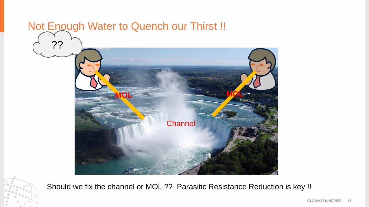
Not Enough Water to Quench our Thirst !!
GLOBALFOUNDRIES 16
Channel
MOL MOL
Should we fix the channel or MOL ?? Parasitic Resistance Reduction is key !!
??

Material Innovation
GLOBALFOUNDRIES 17
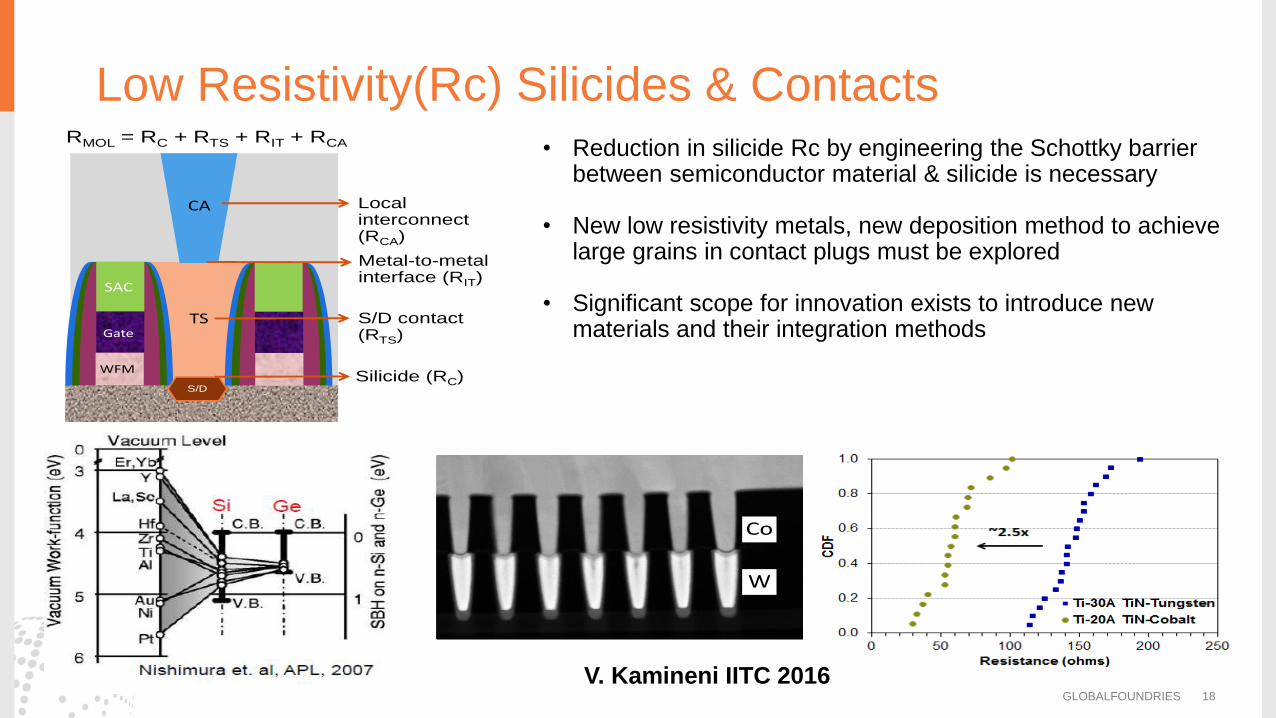
Low Resistivity(Rc) Silicides & Contacts
GLOBALFOUNDRIES 18
• Reduction in silicide Rc by engineering the Schottky barrier between semiconductor material & silicide is necessary
• New low resistivity metals, new deposition method to achieve large grains in contact plugs must be explored
• Significant scope for innovation exists to introduce new
materials and their integration methods
W
Co
SAC
WFM
Gate
S/D
CA
TS
Local interconnect (RCA)
S/D contact (RTS)
Silicide (RC)
Metal-to-metal interface (RIT)
RMOL = RC + RTS + RIT + RCA
V. Kamineni IITC 2016
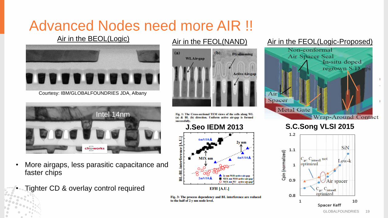
Advanced Nodes need more AIR !!
GLOBALFOUNDRIES 19
Air in the BEOL(Logic)
Intel 14nm
• More airgaps, less parasitic capacitance and faster chips
• Tighter CD & overlay control required
Courtesy: IBM/GLOBALFOUNDRIES JDA, Albany
Air in the FEOL(NAND)
S.C.Song VLSI 2015
Air in the FEOL(Logic-Proposed)
J.Seo IEDM 2013
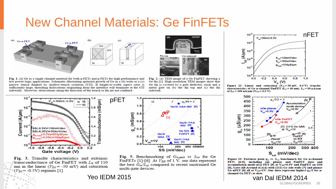
New Channel Materials: Ge FinFETs
GLOBALFOUNDRIES 20
Yeo IEDM 2015 van Dal IEDM 2014
nFET
pFET
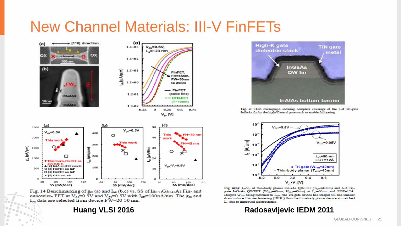
New Channel Materials: III-V FinFETs
GLOBALFOUNDRIES 21
Huang VLSI 2016 Radosavljevic IEDM 2011
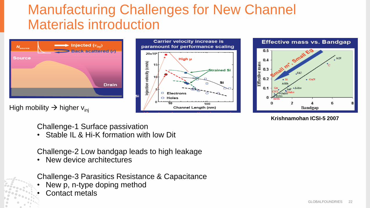
Manufacturing Challenges for New Channel Materials introduction
GLOBALFOUNDRIES 22
Challenge-1 Surface passivation • Stable IL & Hi-K formation with low Dit
Challenge-2 Low bandgap leads to high leakage • New device architectures
Challenge-3 Parasitics Resistance & Capacitance • New p, n-type doping method • Contact metals
High mobility higher vinj
Krishnamohan ICSI-5 2007
New Device Architectures
GLOBALFOUNDRIES 23
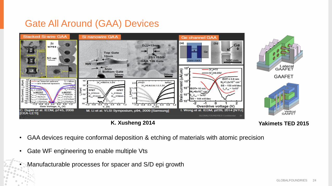
Gate All Around (GAA) Devices
GLOBALFOUNDRIES 24
K. Xusheng 2014
GAAFET
Yakimets TED 2015
• GAA devices require conformal deposition & etching of materials with atomic precision
• Gate WF engineering to enable multiple Vts
• Manufacturable processes for spacer and S/D epi growth
GLOBALFOUNDRIES 25
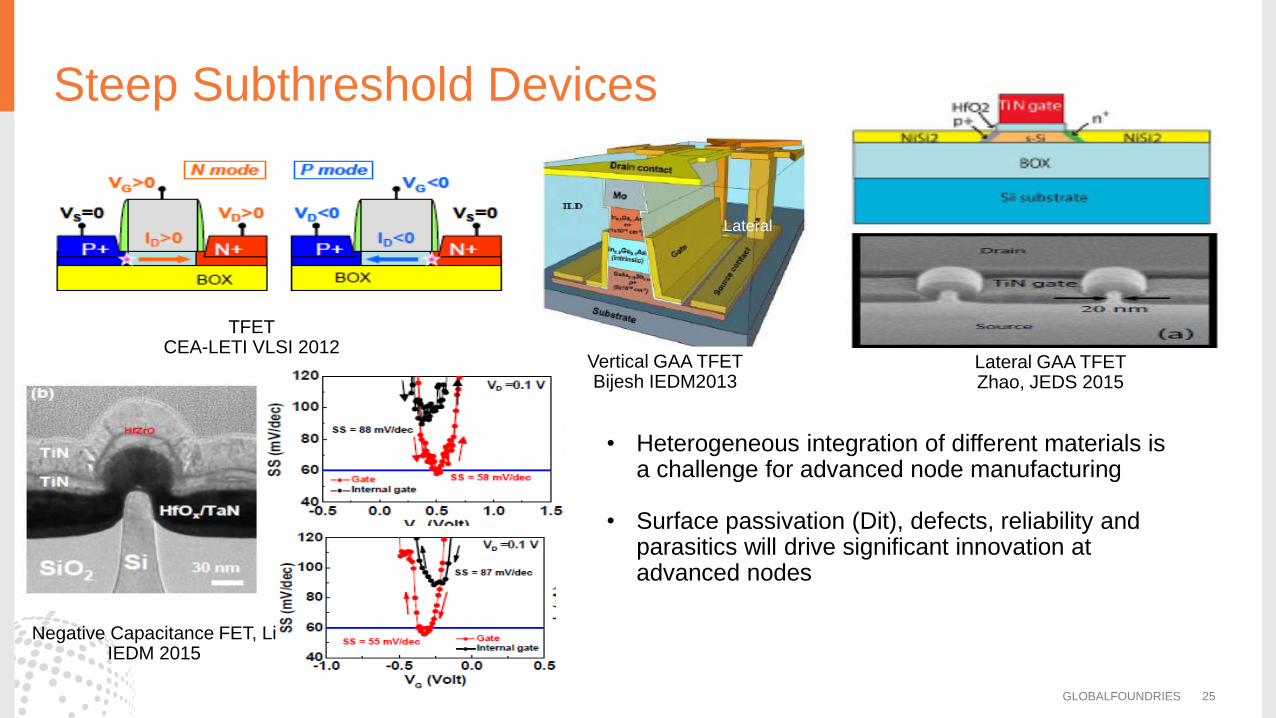
TFET CEA-LETI VLSI 2012
Lateral GAA TFET Zhao, JEDS 2015
Vertical GAA TFET Bijesh IEDM2013
Lateral
Steep Subthreshold Devices
Negative Capacitance FET, Li IEDM 2015
• Heterogeneous integration of different materials is a challenge for advanced node manufacturing
• Surface passivation (Dit), defects, reliability and parasitics will drive significant innovation at advanced nodes
Summary
• Pitch scaling is slowing and follows lithography advances (SAQP, EUV)
• Overlay, CD control, more and more self-aligned architectures are required
for advanced node manufacturing
• Structural integrity, reliability and variability are critical drivers for pitch
scaling at advanced node manufacturing
• Surface passivation, defects, reliability and parasitics(R, C) will drive
introduction of new materials at advanced nodes
• Reducing parasitics and variability in devices and interconnects are must
to achieve best SoC performance per watt per dollar
GLOBALFOUNDRIES 26
© 2014 GLOBALFOUNDRIES Inc. All rights reserved.
Thank you