Embed Size (px)
Citation preview
8/14/2019 Ch3 Com Bi National Logic Design
http://slidepdf.com/reader/full/ch3-com-bi-national-logic-design 1/29
Dr. I. Damaj 1
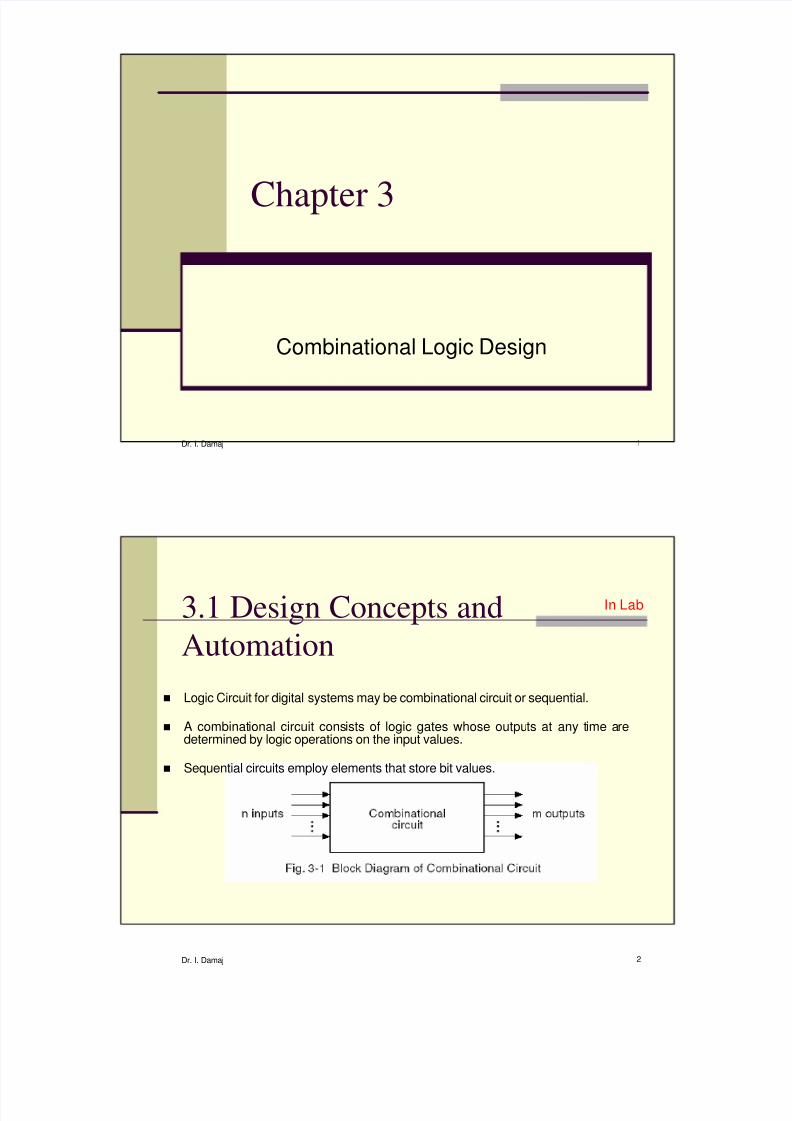
Chapter 3
Combinational Logic Design
Dr. I. Damaj 2
3.1 Design Concepts and
Automation
n Logic Circuit for digital systems may be combinational circuit or sequential.
n A combinational circuit consists of logic gates whose outputs at any time aredetermined by logic operations on the input values.
n Sequential circuits employ elements that store bit values.
In Lab

8/14/2019 Ch3 Com Bi National Logic Design
http://slidepdf.com/reader/full/ch3-com-bi-national-logic-design 2/29
Dr. I. Damaj 3
Design Hierarchy
n A circuit may be specified by a symbol showing its inputs and outputs and a
description defining exactly how it operates.
n A complex digital system may contain millions of interconnected gates (severaltens of millions in the case of VLSI).
n With such complexity, the interconnected gates appear to be like a maze.
n In order to deal with such complexity, the circuit is broken up into pieces that wecall blocks .
n The blocks are interconnected to form the circuit.
n This approach is a “divide an conquer” approach.
n This design approach is referred to as hierarchal design.
In Lab
Dr. I. Damaj 4
Hierarchical Design
n To control the complexity of the function mapping inputs to outputs:
n Decompose the function into smaller pieces called blocks
n Decompose each block’s function into smaller blocks,repeating as necessary until all blocks are small enough
n Any block not decomposed is called a primitive block
n The collection of all blocks including the decomposedones is a hierarchy
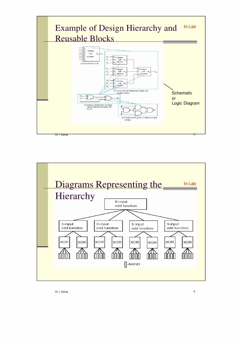
n Example: 9-input parity tree (see next slide)n Top Level: 9 inputs, one output
n 2nd Level: Four 3-bit odd parity trees in two levelsn 3rd Level: Two 2-bit exclusive-OR functions
n Primitives: Four 2- input NAND gatesn Design requires 4 X 2 X 4 = 32 2-input NAND gates
In Lab
8/14/2019 Ch3 Com Bi National Logic Design
http://slidepdf.com/reader/full/ch3-com-bi-national-logic-design 3/29
Dr. I. Damaj 5
Example of Design Hierarchy and
Reusable Blocks
Schematic
orLogic Diagram
In Lab
Dr. I. Damaj 6
Diagrams Representing the
Hierarchy
In Lab

8/14/2019 Ch3 Com Bi National Logic Design
http://slidepdf.com/reader/full/ch3-com-bi-national-logic-design 4/29
Dr. I. Damaj 7
Design Hierarchy
n
A hierarchy reduces the complexity of required torepresent the schematic diagram of the circuit.
n A hierarchy ends at a set of leaves called primitive blocks .
n With hierarchal design, reusability is one of the mostimportant properties.
In Lab
Dr. I. Damaj 8
Top-Down versus Bottom-Up
n A top-down design proceeds from an abstract, high-levelspecification to a more and more detailed design bydecomposition and successive refinement
n A bottom-up design starts with detailed primitive blocks andcombines them into larger and more complex functional blocks
n Designs usually proceed from both directions simultaneouslyn Top-down design answers: What are we building?
n Bottom-up design answers: How do we build it?
n Top-down controls complexity while bottom-up focuses on thedetails
In Lab

8/14/2019 Ch3 Com Bi National Logic Design
http://slidepdf.com/reader/full/ch3-com-bi-national-logic-design 5/29
Dr. I. Damaj 9
Top-Down Design
n Ideally, the design process is performed top-down. This means
that the logic function is specified typically by text or a hardwaredescription language (HDL).
n At high levels of the design, the circuit is then repeatedly dividedinto blocks as necessary until the blocks are small enough toperform logic design.
n In order to obtain reusability and to make maximum use ofpredefined modules, it is often necessary to perform portions ofthe design bottom up .
In Lab
Dr. I. Damaj 10
Reusable Functions and CAD
n Whenever possible, we try to decompose a complex design intocommon, reusable function blocks
n These blocks are
n verified and well-documented
n placed in libraries for future use
n
Representative Computer-Aided Design Tools:n Schematic Capture
n Logic Simulators
n Timing Verifiers
n Hardware Description Languages
n Verilog and VHDL
n Logic Synthesizers
n Integrated Circuit Layout
In Lab
8/14/2019 Ch3 Com Bi National Logic Design
http://slidepdf.com/reader/full/ch3-com-bi-national-logic-design 6/29
Dr. I. Damaj 11
Hardware Description Languages
n Hardware description languages resemble programming languages, but are
specifically oriented to describing hardware structures and behavior.
n They differ from typical programming languages in that they represent extensiveparallel operation whereas most programming languages represent serialoperation.
n HDLs provide an alternative to schematics.
n When a language is used in this fashion, it is referred to as a structural descriptionin which the language describes an interconnection of components.
n Such a structural description, referred to as a netlist, can be used as an input tologic simulation just as a schematic is used.
n
A major reason for the growth of the use of HDLs is logic synthesis.
In Lab
Dr. I. Damaj 12
Logic Synthesis
n Logic synthesis transforms an RTL description of acircuit in an HDL into an optimized netlist representingstorage elements and combinational logic.
n This netlist may be transformed by using physicaldesign tools into an actual integrated circuit layout.This layout serves as the basis for integrated circuitmanufacture.
In Lab

8/14/2019 Ch3 Com Bi National Logic Design
http://slidepdf.com/reader/full/ch3-com-bi-national-logic-design 7/29
Dr. I. Damaj 13
High-Level Flow for Synthesis
Tool
In Lab
Dr. I. Damaj 14
3.2 The Design Space
Gate Properties
n Digital circuits are constructed with integrated circuits (ICs).
n An IC is a semiconductor crystal, informally called a chip,containing the electronic components for the digital gates and
storage elements.
n The various components are interconnected on the chip.
n The ship is mounted in a ceramic or plastic container, andconnections are welded from the chip to the external pins toform the IC.
In Lab

8/14/2019 Ch3 Com Bi National Logic Design
http://slidepdf.com/reader/full/ch3-com-bi-national-logic-design 8/29
Dr. I. Damaj 15
Integrated Circuits
n Integrated circuit (informally, a “chip”) is a semiconductor
crystal (most often silicon) containing the electroniccomponents for the digital gates and storage elementswhich are interconnected on the chip.
n Terminology - Levels of chip integration
n SSI (small-scale integrated ) - fewer than 10 gates
n MSI (medium-scale integrated ) - 10 to 100 gates
n LSI (large-scale integrated ) - 100 to thousands of gates
n VLSI (very large-scale integrated ) - thousands to 100s ofmillions of gates
In Lab
Dr. I. Damaj 16
n ICs are classified not only by their function, but also by their specificimplementation technology.
n Each technology has its own basic electronic device and circuitstructure.
n Currently, silicon-based Complementary Metal Oxide Semiconductor(CMOS) technology dominates due to:n its high circuit density,n high performance,
n and low power consumption.
n Alternative technologies based on Gallium Arsenide (GaAs) and SiliconGermanium (SiGe) are used selectively for very high speed circuits.
Circuit TechnologiesIn Lab
8/14/2019 Ch3 Com Bi National Logic Design
http://slidepdf.com/reader/full/ch3-com-bi-national-logic-design 9/29
Dr. I. Damaj 17
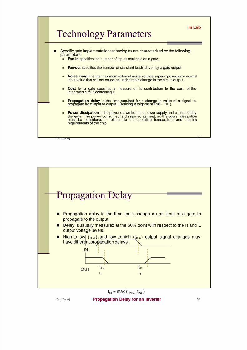
n Specific gate implementation technologies are characterized by the followingparameters:n Fan-in specifies the number of inputs available on a gate.
n Fan-out specifies the number of standard loads driven by a gate output.
n Noise margin is the maximum external noise voltage superimposed on a normalinput value that will not cause an undesirable change in the circuit output.
n Cost for a gate specifies a measure of its contribution to the cost of theintegrated circuit containing it.
n Propagation delay is the time required for a change in value of a signal topropagate from input to output. (Reading Assignment P98 – 101).
n Power dissipation is the power drawn from the power supply and consumed bythe gate. The power consumed is dissipated as heat, so the power dissipationmust be considered in relation to the operating temperature and cooling
requirements of the chip.
Technology ParametersIn Lab
Dr. I. Damaj 18
Propagation Delay
n Propagation delay is the time for a change on an input of a gate to
propagate to the output.
n Delay is usually measured at the 50% point with respect to the H and Loutput voltage levels.
n High-to-low (tPHL) and low-to-high (tPLH) output signal changes mayhave different propagation delays.
tPH
L
tPL
H
IN
OUT
tpd = max (tPHL, tPLH)
Propagation Delay for an Inverter

8/14/2019 Ch3 Com Bi National Logic Design
http://slidepdf.com/reader/full/ch3-com-bi-national-logic-design 10/29
Dr. I. Damaj 19
Delay Models
n Transport delay - a change in the output in response
to a change on the inputs occurs after a fixedspecified delay
n Inertial delay - similar to transport delay, except that ifthe input changes such that the output is to changetwice in a time interval less than the rejection time ,the output changes do not occur. Models typical
electronic circuit behavior, namely, rejects narrow“pulses” on the outputs
Dr. I. Damaj 20
Delay Model Example
A
A B:
TransportDelay (TD)
InertialDelay (ID)
B
Time (ns)0 42 6 8 10 12 14 16
No Delay(ND) a b c d e
Propagation Delay = 2.0 ns Rejection Time = 1 .0 ns
8/14/2019 Ch3 Com Bi National Logic Design
http://slidepdf.com/reader/full/ch3-com-bi-national-logic-design 11/29
Dr. I. Damaj 21
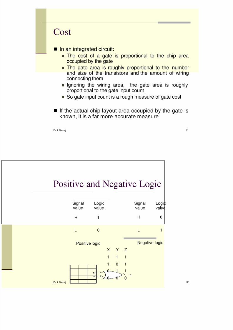
Cost
n In an integrated circuit:n
The cost of a gate is proportional to the chip areaoccupied by the gate
n The gate area is roughly proportional to the numberand size of the transistors and the amount of wiringconnecting them
n Ignoring the wiring area, the gate area is roughlyproportional to the gate input count
n So gate input count is a rough measure of gate cost
n If the actual chip layout area occupied by the gate is
known, it is a far more accurate measure
Dr. I. Damaj 22
Positive and Negative Logic
Signalvalue
Logicvalue
Signalvalue
Logicvalue
H 1 H 0
L 0 L 1
Positive logic Negative logic
110
000
101
111
ZYX
8/14/2019 Ch3 Com Bi National Logic Design
http://slidepdf.com/reader/full/ch3-com-bi-national-logic-design 12/29
Dr. I. Damaj 23
3.3 Design Procedure
n The design of a combinational circuit starts from the specification of theproblem and ends in a logic diagram or netlist that describes a logic
diagram. The procedure involves the following steps:n Specification.n Formulation.
n Optimization.
n Technology Mapping.n Verification.
n The specification can take a variety of forms such as text or an HDLdescription and should include the respective symbols or names for theinputs and outputs.
n Formulation converts the specification into forms that can be optimized.n Optimization can be performed by any of a number of available methods:
n Algebraic manipulation.
n K-maps.n Computer-based simplification programs.
Dr. I. Damaj 24
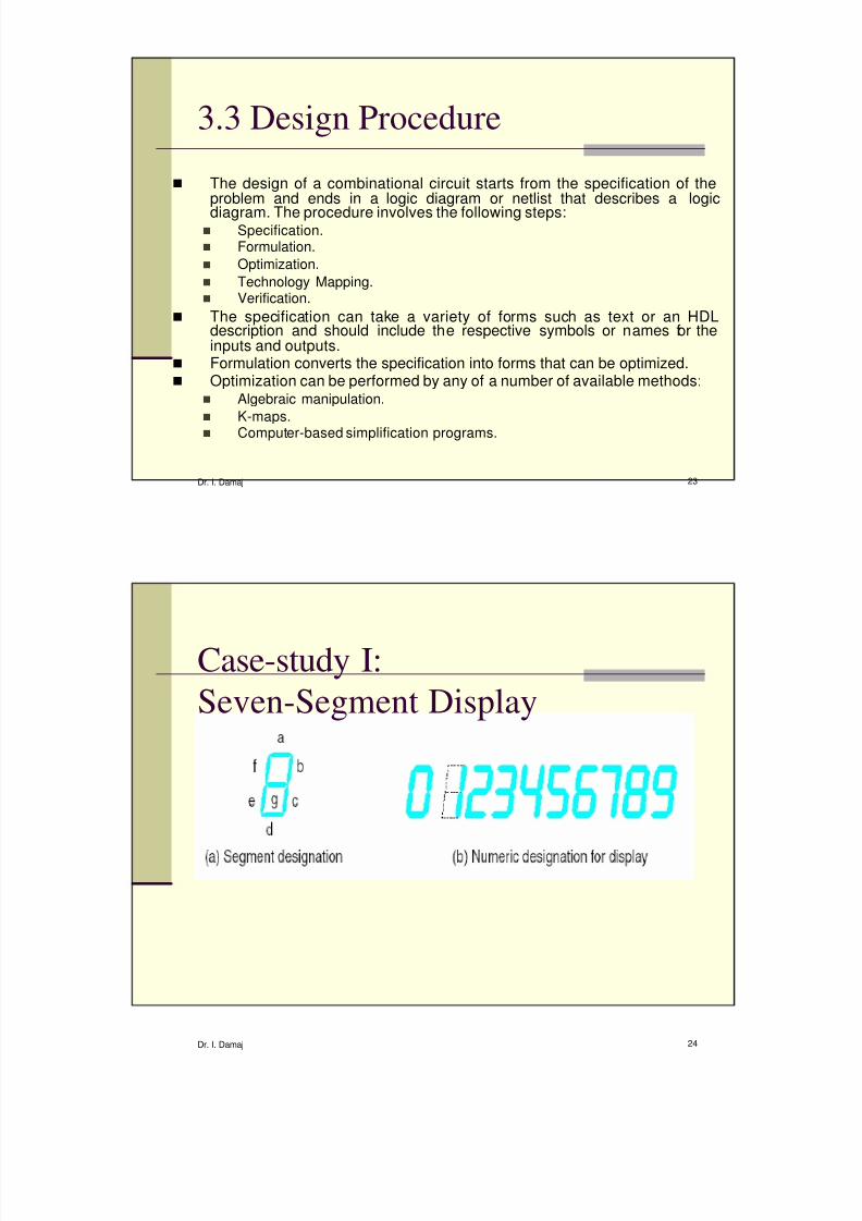
Case-study I:
Seven-Segment Display
8/14/2019 Ch3 Com Bi National Logic Design
http://slidepdf.com/reader/full/ch3-com-bi-national-logic-design 13/29
Dr. I. Damaj 25
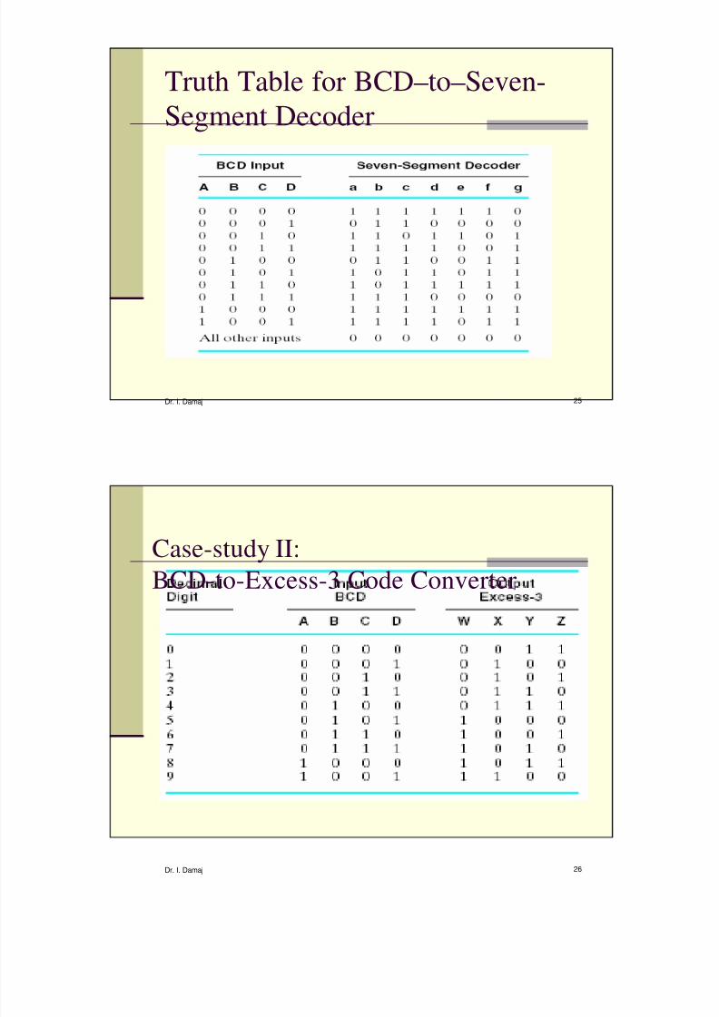
Truth Table for BCD–to–Seven-
Segment Decoder
Dr. I. Damaj 26
Case-study II:
BCD-to-Excess-3 Code Converter
8/14/2019 Ch3 Com Bi National Logic Design
http://slidepdf.com/reader/full/ch3-com-bi-national-logic-design 14/29
Dr. I. Damaj 27
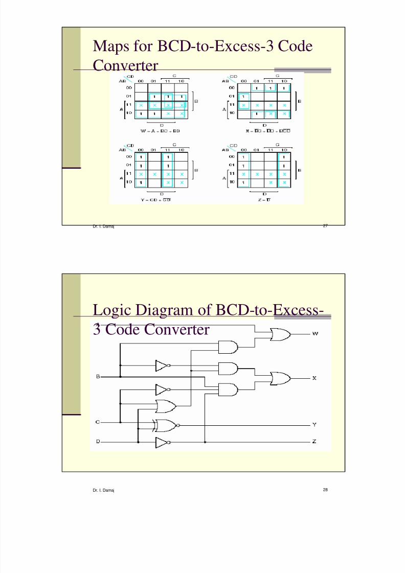
Maps for BCD-to-Excess-3 Code
Converter
Dr. I. Damaj 28
Logic Diagram of BCD-to-Excess-
3 Code Converter
8/14/2019 Ch3 Com Bi National Logic Design
http://slidepdf.com/reader/full/ch3-com-bi-national-logic-design 15/29
Dr. I. Damaj 29
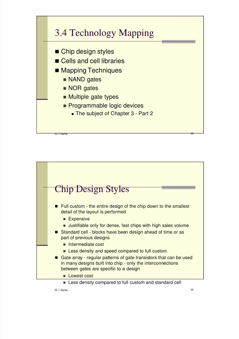
3.4 Technology Mapping
n Chip design styles
n Cells and cell libraries
n Mapping Techniques
n NAND gates
n NOR gates
n Multiple gate types
n Programmable logic devices
n The subject of Chapter 3 - Part 2
Dr. I. Damaj 30
Chip Design Styles
n Full custom - the entire design of the chip down to the smallest
detail of the layout is performed
n Expensive
n Justifiable only for dense, fast chips with high sales volume
n Standard cell - blocks have been design ahead of time or as
part of previous designsn Intermediate cost
n Less density and speed compared to full custom
n Gate array - regular patterns of gate transistors that can be used
in many designs built into chip - only the interconnections
between gates are specific to a design
n Lowest cost
n Less density compared to full custom and standard cell

8/14/2019 Ch3 Com Bi National Logic Design
http://slidepdf.com/reader/full/ch3-com-bi-national-logic-design 16/29
Dr. I. Damaj 31
Cell Libraries
n Cell - a pre-designed primitive block
n Cell library - a collection of cells available for designusing a particular implementation technology
n Cell characterization - a detailed specification of acell for use by a designer - often based on actual cell
design and fabrication and measured values
n Cells are used for gate array, standard cell, and insome cases, full custom chip design
Dr. I. Damaj 32
n Schematic or logic diagram
n Area of cell
n Often normalized to the area of a common, small cell such as an
inverter
n Input loading (in standard loads) presented to outputs driving each of
the inputs
n Delays from each input to each output
n One or more cell templates for technology mapping
n One or more hardware description language models
n If automatic layout is to be used:
n Physical layout of the cell circuit
n A floorplan layout providing the location of inputs, outputs, power
and ground connections on the cell
Typical Cell Characterization Components

8/14/2019 Ch3 Com Bi National Logic Design
http://slidepdf.com/reader/full/ch3-com-bi-national-logic-design 17/29
Dr. I. Damaj 33
Example Cell Library
CellName
CellSchematic
NormalizedArea
Typical
InputLoad
TypicalInput-to-
OutputDelay
Basic
FunctionTemplates
Inverter 1.00 1.000.04
1 0.0123 SL
2NAND 1.25 1.000.05
1 0.0143 SL
2NOR 1.25 1.000.06
1 0.0183 SL
2-2 AOI 2.25 0.95
0.07
1 0.0193 SL
Dr. I. Damaj 34
Mapping to NAND gates
n Assumptions:n Gate loading and delay are ignored
n Cell library contains an inverter and n -input NANDgates, n = 2, 3, …
n An AND, OR, inverter schematic for the circuit isavailable
n The mapping is accomplished by:n Replacing AND and OR symbols,
n Pushing inverters through circuit fan-out points, and
n Canceling inverter pairs
8/14/2019 Ch3 Com Bi National Logic Design
http://slidepdf.com/reader/full/ch3-com-bi-national-logic-design 18/29
Dr. I. Damaj 35
NAND Mapping Algorithm
1. Replace ANDs and ORs:
2. Repeat the following pair of actions until there is atmost one inverter between:
a. A circuit input or driving NAND gate output, and
b. The attached NAND gate inputs.
.
.
.
.
.
.
.
.
.
.
.
.
.
.
.
.
.
.
Dr. I. Damaj 36
NAND Mapping Example
A
B
C
D
F
E
(a)
A
B
C
7
5
1
6
2
4
9
X
Y
38D
E
F
(b)
A
B
C
D
E
F
(d)
X
5
5
7
6Y
(c)
OI
8/14/2019 Ch3 Com Bi National Logic Design
http://slidepdf.com/reader/full/ch3-com-bi-national-logic-design 19/29
Dr. I. Damaj 37
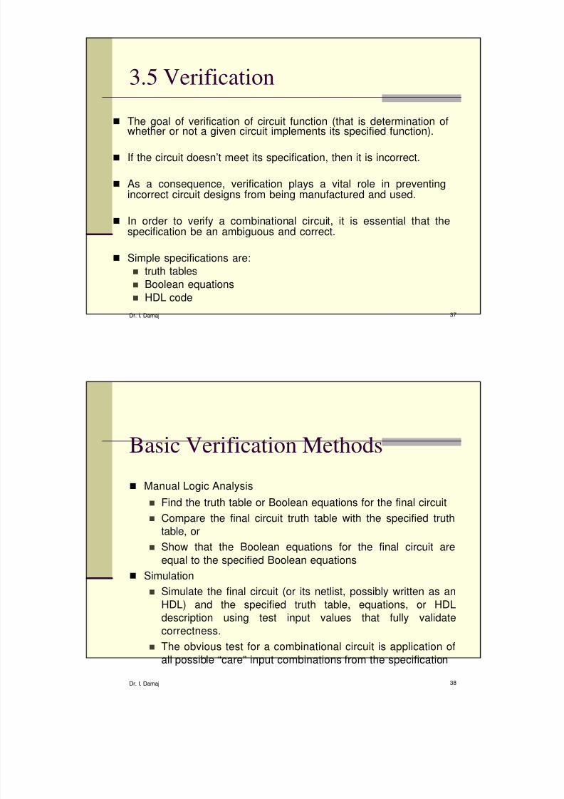
3.5 Verification
n The goal of verification of circuit function (that is determination ofwhether or not a given circuit implements its specified function).
n If the circuit doesn’t meet its specification, then it is incorrect.
n As a consequence, verification plays a vital role in preventingincorrect circuit designs from being manufactured and used.
n In order to verify a combinational circuit, it is essential that thespecification be an ambiguous and correct.
n Simple specifications are:
n truth tables
n Boolean equations
n HDL code
Dr. I. Damaj 38
Basic Verification Methods
n Manual Logic Analysis
n Find the truth table or Boolean equations for the final circuit
n Compare the final circuit truth table with the specified truth
table, or
n Show that the Boolean equations for the final circuit are
equal to the specified Boolean equationsn Simulation
n Simulate the final circuit (or its netlist, possibly written as an
HDL) and the specified truth table, equations, or HDL
description using test input values that fully validate
correctness.
n The obvious test for a combinational circuit is application of
all possible “care” input combinations from the specification
8/14/2019 Ch3 Com Bi National Logic Design
http://slidepdf.com/reader/full/ch3-com-bi-national-logic-design 20/29
Dr. I. Damaj 39
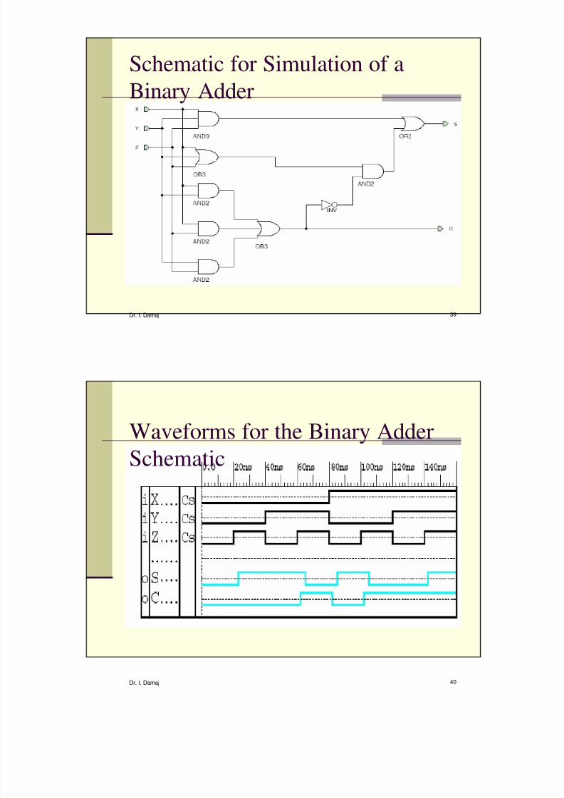
Schematic for Simulation of a
Binary Adder
Dr. I. Damaj 40
Waveforms for the Binary Adder
Schematic
8/14/2019 Ch3 Com Bi National Logic Design
http://slidepdf.com/reader/full/ch3-com-bi-national-logic-design 21/29
Dr. I. Damaj 41
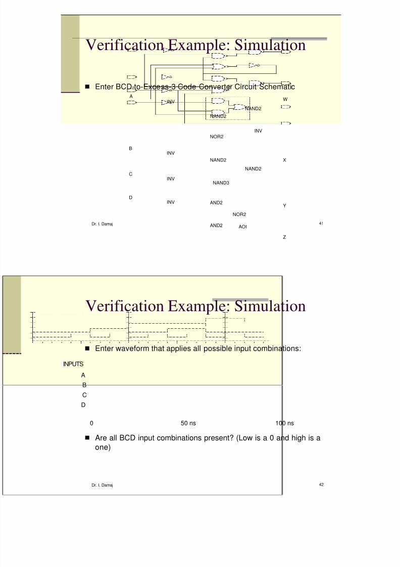
Verification Example: Simulation
n Enter BCD-to-Excess-3 Code Converter Circuit Schematic
NAND2
NAND2
INV
NOR2
INV
NAND2
INV
NAND2
AND2
AND2
NAND3INV
INV
NOR2
W
B
A
C
D
X
AOI
Y
Z
Dr. I. Damaj 42
Verification Example: Simulation
n Enter waveform that applies all possible input combinations:
n Are all BCD input combinations present? (Low is a 0 and high is a
one)
0 50 ns 100 ns
INPUTS
A
B
C
D
8/14/2019 Ch3 Com Bi National Logic Design
http://slidepdf.com/reader/full/ch3-com-bi-national-logic-design 22/29
Dr. I. Damaj 43
3.6 Why Programmable Logic?
n Facts:n
It is most economical to produce an IC in large volumesn Many designs required only small volumes of ICs
n Need an IC that can be:n Produced in large volumes
n Handle many designs required in small volumes
n A programmable logic part can be:n made in large volumes
n programmed to implement large numbers of differentlow-volume designs
Dr. I. Damaj 44
Programmable Logic - Additional
Advantages
n Many programmable logic devices are field- programmable , i. e.,can be programmed outside of the manufacturing environment
n Most programmable logic devices are erasable andreprogrammable .
n Allows “updating” a device or correction of errors
n Allows reuse the device for a different design - the ultimatein re-usability!
n Ideal for course laboratories
n Programmable logic devices can be used to prototype design thatwill be implemented for sale in regular ICs.
n Complete Intel Pentium designs were actually prototypewith specialized systems based on large numbers of VLSIprogrammable devices!
8/14/2019 Ch3 Com Bi National Logic Design
http://slidepdf.com/reader/full/ch3-com-bi-national-logic-design 23/29
Dr. I. Damaj 45
Programming Technologies
nProgramming technologies are used to:
nControl connections
nBuild lookup tables
nControl transistor switching
nThe technologies
nControl connections
n Mask programming
n Fuse
n Antifusen Single-bit storage element
Dr. I. Damaj 46
Programming Technologies
nThe technologies (continued)
nBuild lookup tables
n Storage elements (as in a memory)
nTransistor Switching Control
n Stored charge on a floating transistor gate
§ Erasable
§ Electrically erasable
§ Flash (as in Flash Memory)
n Storage elements (as in a memory)
8/14/2019 Ch3 Com Bi National Logic Design
http://slidepdf.com/reader/full/ch3-com-bi-national-logic-design 24/29
Dr. I. Damaj 47
Technology Characteristics
n Permanent - Cannot be erased and reprogrammed
n Mask programmingn Fuse
n Antifuse
Dr. I. Damaj 48
Technology Characteristics
n Reprogrammable
n Volatile - Programming lost if chip power lost
n Single-bit storage element
n Non-Volatile
n Erasable
n Electrically erasable
n
Flash (as in Flash Memory)n Build lookup tables
n Storage elements (as in a memory)
n Transistor Switching Control
n Stored charge on a floating transistor gate
§ Erasable
§ Electrically erasable
§ Flash (as in Flash Memory)
n Storage elements (as in a memory)
8/14/2019 Ch3 Com Bi National Logic Design
http://slidepdf.com/reader/full/ch3-com-bi-national-logic-design 25/29
Dr. I. Damaj 49
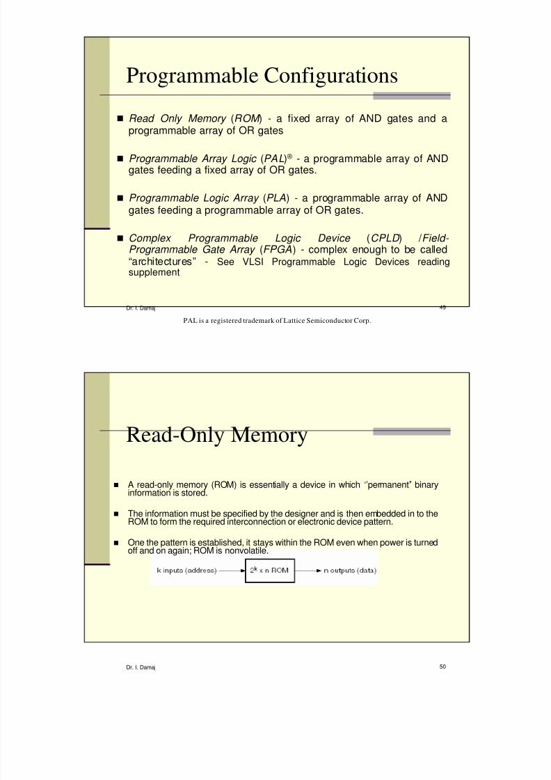
Programmable Configurations
n Read Only Memory (ROM ) - a fixed array of AND gates and aprogrammable array of OR gates
n Programmable Array Logic (PAL)® - a programmable array of ANDgates feeding a fixed array of OR gates.
n Programmable Logic Array (PLA) - a programmable array of ANDgates feeding a programmable array of OR gates.
n Complex Programmable Logic Device (CPLD ) / Field- Programmable Gate Array (FPGA) - complex enough to be called“architectures” - See VLSI Programmable Logic Devices reading
supplement
PAL is a registered trademark of Lattice Semiconductor Corp.
Dr. I. Damaj 50
Read-Only Memory
n A read-only memory (ROM) is essentially a device in which ‘’permanent’’ binaryinformation is stored.
n The information must be specified by the designer and is then embedded in to theROM to form the required interconnection or electronic device pattern.
n
One the pattern is established, it stays within the ROM even when power is turnedoff and on again; ROM is nonvolatile.
8/14/2019 Ch3 Com Bi National Logic Design
http://slidepdf.com/reader/full/ch3-com-bi-national-logic-design 26/29
Dr. I. Damaj 51
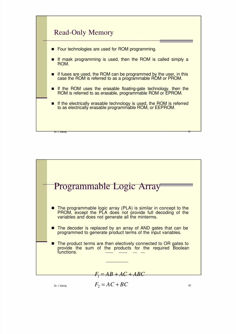
Read-Only Memory
n Four technologies are used for ROM programming.
n If mask programming is used, then the ROM is called simply aROM.
n If fuses are used, the ROM can be programmed by the user, in thiscase the ROM is referred to as a programmable ROM or PROM.
n If the ROM uses the erasable floating-gate technology, then theROM is referred to as erasable, programmable ROM or EPROM.
n If the electrically erasable technology is used, the ROM is referredto as electrically erasable programmable ROM, or EEPROM.
Dr. I. Damaj 52
Programmable Logic Array
n The programmable logic array (PLA) is similar in concept to thePROM, except the PLA does not provide full decoding of thevariables and does not generate all the minterms.
n The decoder is replaced by an array of AND gates that can be
programmed to generate product terms of the input variables.
n The product terms are then electively connected to OR gates toprovide the sum of the products for the required Booleanfunctions.
1
2
F AB AC ABC
F AC BC
= + +
= +

8/14/2019 Ch3 Com Bi National Logic Design
http://slidepdf.com/reader/full/ch3-com-bi-national-logic-design 27/29
Dr. I. Damaj 53
Programmable Logic Array
1
2
F AB AC ABC
F AC BC
= + +
= +
Dr. I. Damaj 54
Programmable Logic Array
8/14/2019 Ch3 Com Bi National Logic Design
http://slidepdf.com/reader/full/ch3-com-bi-national-logic-design 28/29
Dr. I. Damaj 55
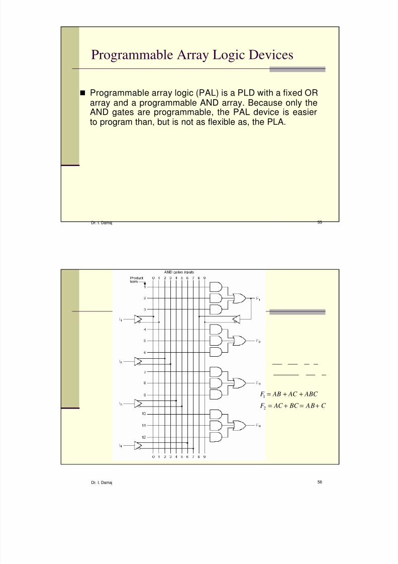
Programmable Array Logic Devices
n Programmable array logic (PAL) is a PLD with a fixed ORarray and a programmable AND array. Because only theAND gates are programmable, the PAL device is easierto program than, but is not as flexible as, the PLA.
Dr. I. Damaj 56
1
2
F AB AC ABC
F AC BC AB C
= + +
= + = +
8/14/2019 Ch3 Com Bi National Logic Design
http://slidepdf.com/reader/full/ch3-com-bi-national-logic-design 29/29
Dr. I. Damaj 57
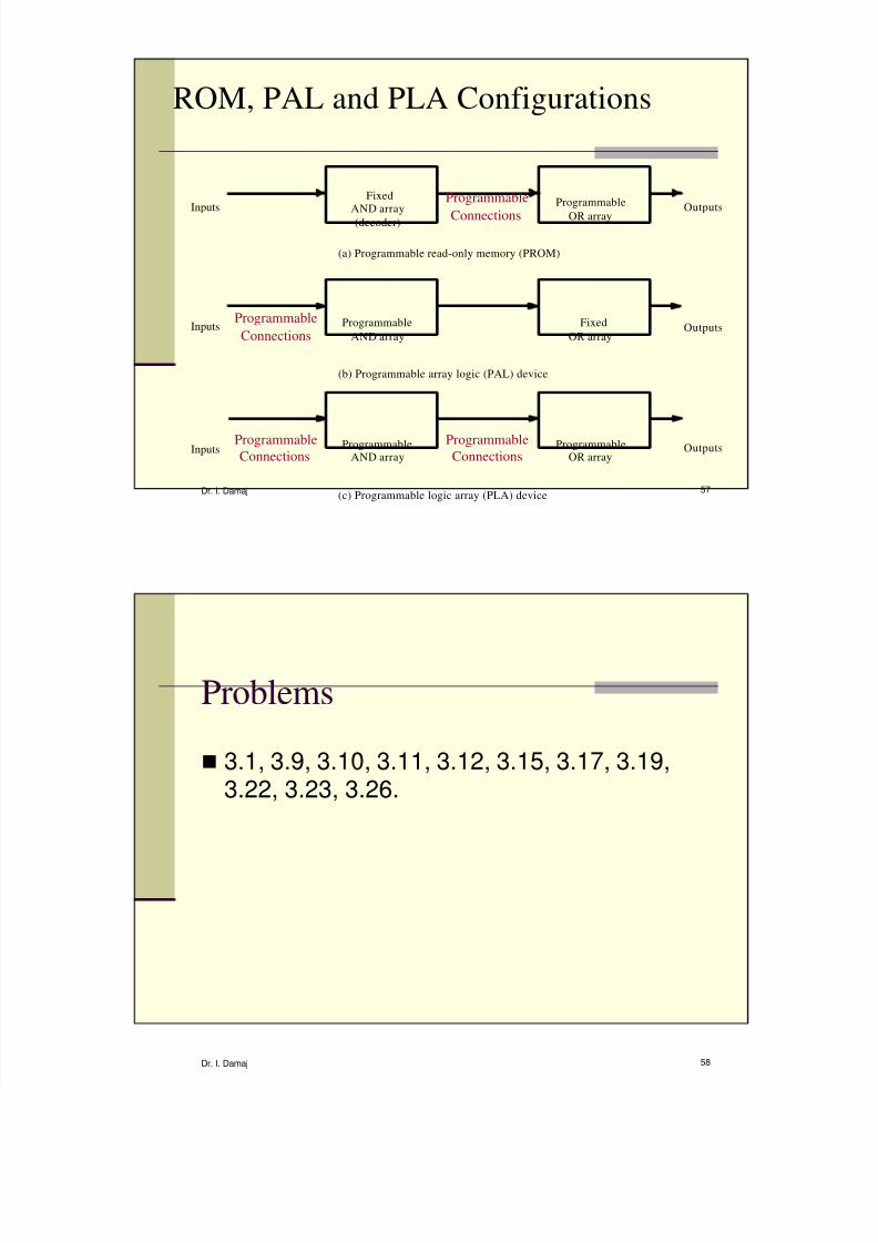
ROM, PAL and PLA Configurations
(a) Programmable read-only memory (PROM)
InputsFixed
AND array
(decoder)
Programmable
OR array
OutputsProgrammable
Connections
(b) Programmable array logic (PAL) device
Inputs Programmable
AND array
Fixed
OR arrayOutputs
Programmable
Connections
(c) Programmable logic array (PLA) device
Inputs ProgrammableOR array
OutputsProgrammableConnections
ProgrammableConnections
ProgrammableAND array
58
Problems
n 3.1, 3.9, 3.10, 3.11, 3.12, 3.15, 3.17, 3.19,3.22, 3.23, 3.26.