Embed Size (px)
Citation preview
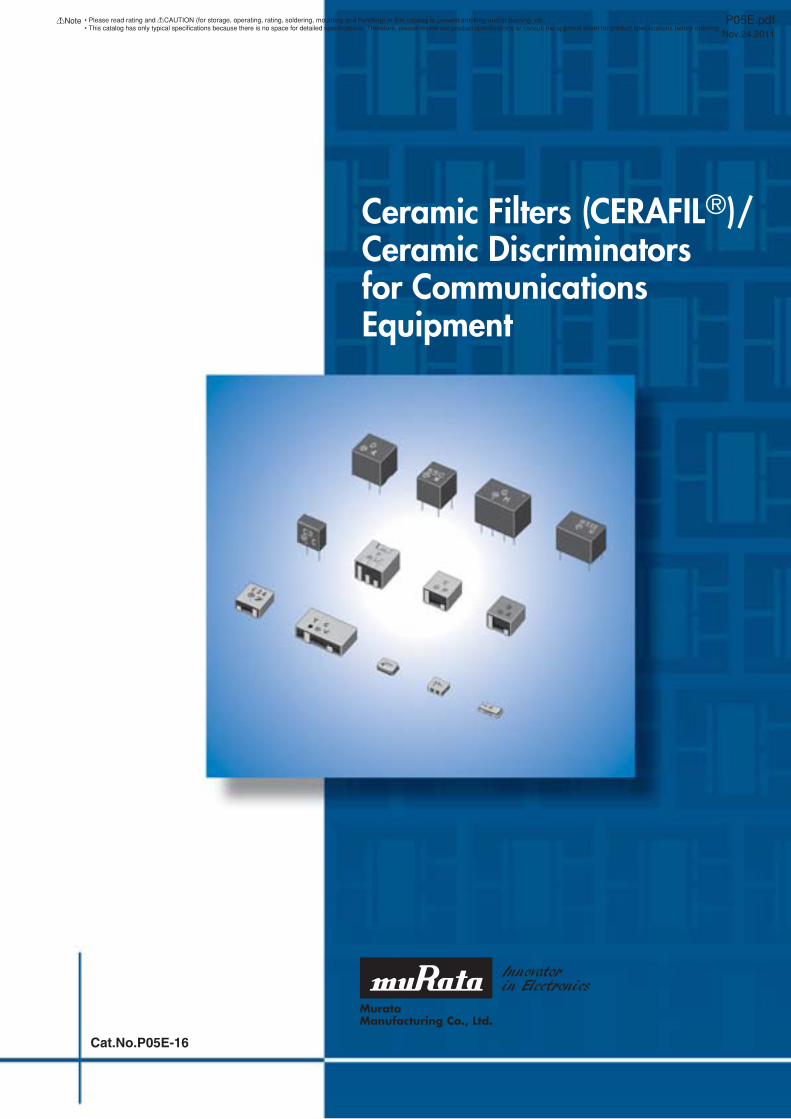
Cat.No.P05E-16
Ceramic Filters (CERAFILr)/Ceramic Discriminators for Communications Equipment
!Note P05E.pdfNov.24,2011
• Please read rating and !CAUTION (for storage, operating, rating, soldering, mounting and handling) in this catalog to prevent smoking and/or burning, etc.• This catalog has only typical specifi cations because there is no space for detailed specifi cations. Therefore, please review our product specifi cations or consult the approval sheet for product specifi cations before ordering.
EU RoHS Compliant All the products in this catalog comply with EU RoHS. EU RoHS is "the European Directive 2011/65/EU on the Restriction of the Use
of Certain Hazardous Substances in Electrical and Electronic Equipment." For more details, please refer to our website 'Murata's Approach for EU RoHS'
(http://www.murata.com/info/rohs.html).
!Note P05E.pdfNov.24,2011
• Please read rating and !CAUTION (for storage, operating, rating, soldering, mounting and handling) in this catalog to prevent smoking and/or burning, etc.• This catalog has only typical specifi cations because there is no space for detailed specifi cations. Therefore, please review our product specifi cations or consult the approval sheet for product specifi cations before ordering.
CERAFILr and "CERAFIL" in this catalog are the trademarks of Murata Manufacturing Co., Ltd.
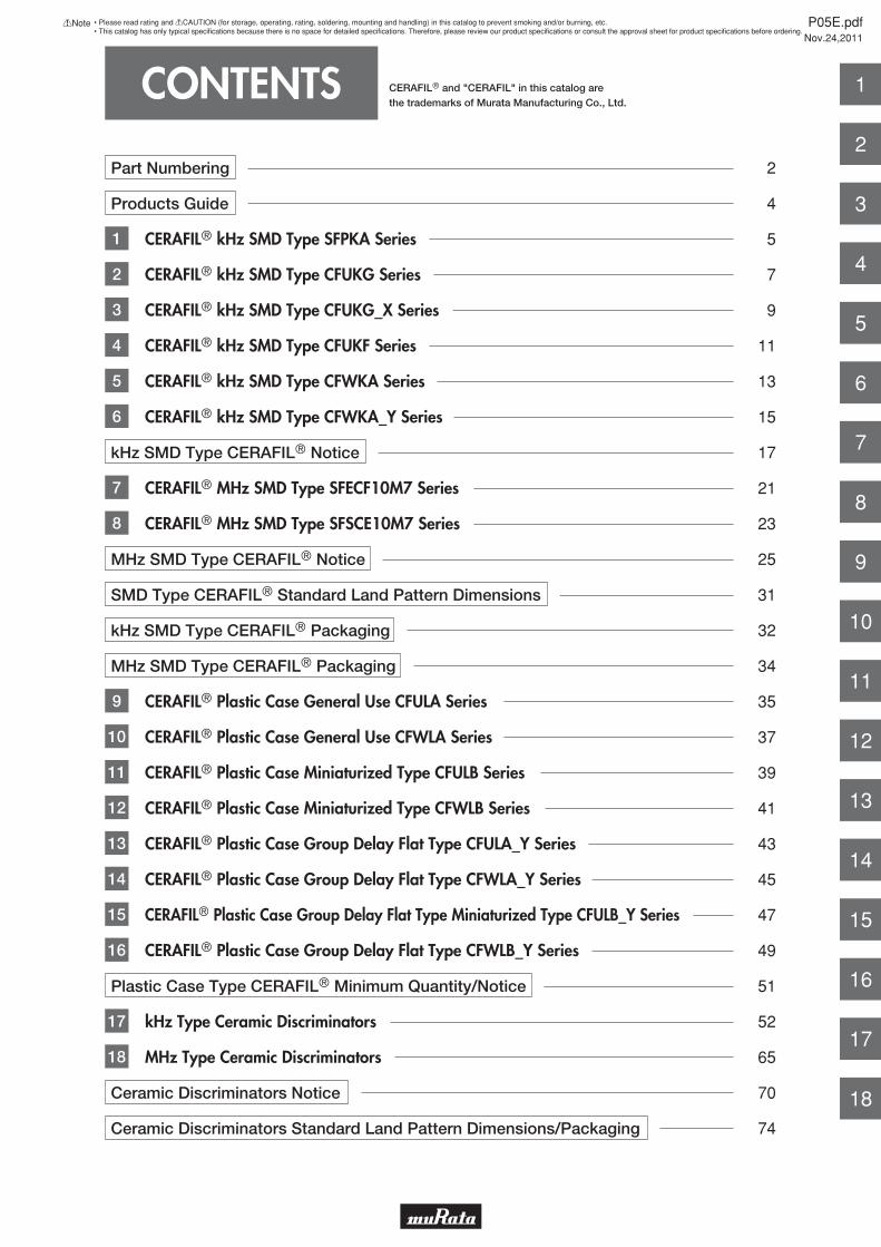
CONTENTS
Part Numbering 2
Products Guide 4
CERAFILr kHz SMD Type SFPKA Series 5
CERAFILr kHz SMD Type CFUKG Series 7
CERAFILr kHz SMD Type CFUKG_X Series 9
CERAFILr kHz SMD Type CFUKF Series 11
CERAFILr kHz SMD Type CFWKA Series 13
CERAFILr kHz SMD Type CFWKA_Y Series 15
kHz SMD Type CERAFILr Notice 17
CERAFILr MHz SMD Type SFECF10M7 Series 21
CERAFILr MHz SMD Type SFSCE10M7 Series 23
MHz SMD Type CERAFILr Notice 25
SMD Type CERAFILr Standard Land Pattern Dimensions 31
kHz SMD Type CERAFILr Packaging 32
MHz SMD Type CERAFILr Packaging 34
CERAFILr Plastic Case General Use CFULA Series 35
CERAFILr Plastic Case General Use CFWLA Series 37
CERAFILr Plastic Case Miniaturized Type CFULB Series 39
CERAFILr Plastic Case Miniaturized Type CFWLB Series 41
CERAFILr Plastic Case Group Delay Flat Type CFULA_Y Series 43
CERAFILr Plastic Case Group Delay Flat Type CFWLA_Y Series 45
CERAFILr Plastic Case Group Delay Flat Type Miniaturized Type CFULB_Y Series 47
CERAFILr Plastic Case Group Delay Flat Type CFWLB_Y Series 49
Plastic Case Type CERAFILr Minimum Quantity/Notice 51
kHz Type Ceramic Discriminators 52
MHz Type Ceramic Discriminators 65
Ceramic Discriminators Notice 70
Ceramic Discriminators Standard Land Pattern Dimensions/Packaging 74
1
2
3
4
5
6
7
8
9
10
11
12
13
14
15
16
17
18
1
2
3
4
5
6
7
8
9
10
11
12
13
14
15
16
17
18
!Note P05E.pdfNov.24,2011
• Please read rating and !CAUTION (for storage, operating, rating, soldering, mounting and handling) in this catalog to prevent smoking and/or burning, etc.• This catalog has only typical specifi cations because there is no space for detailed specifi cations. Therefore, please review our product specifi cations or consult the approval sheet for product specifi cations before ordering.
2
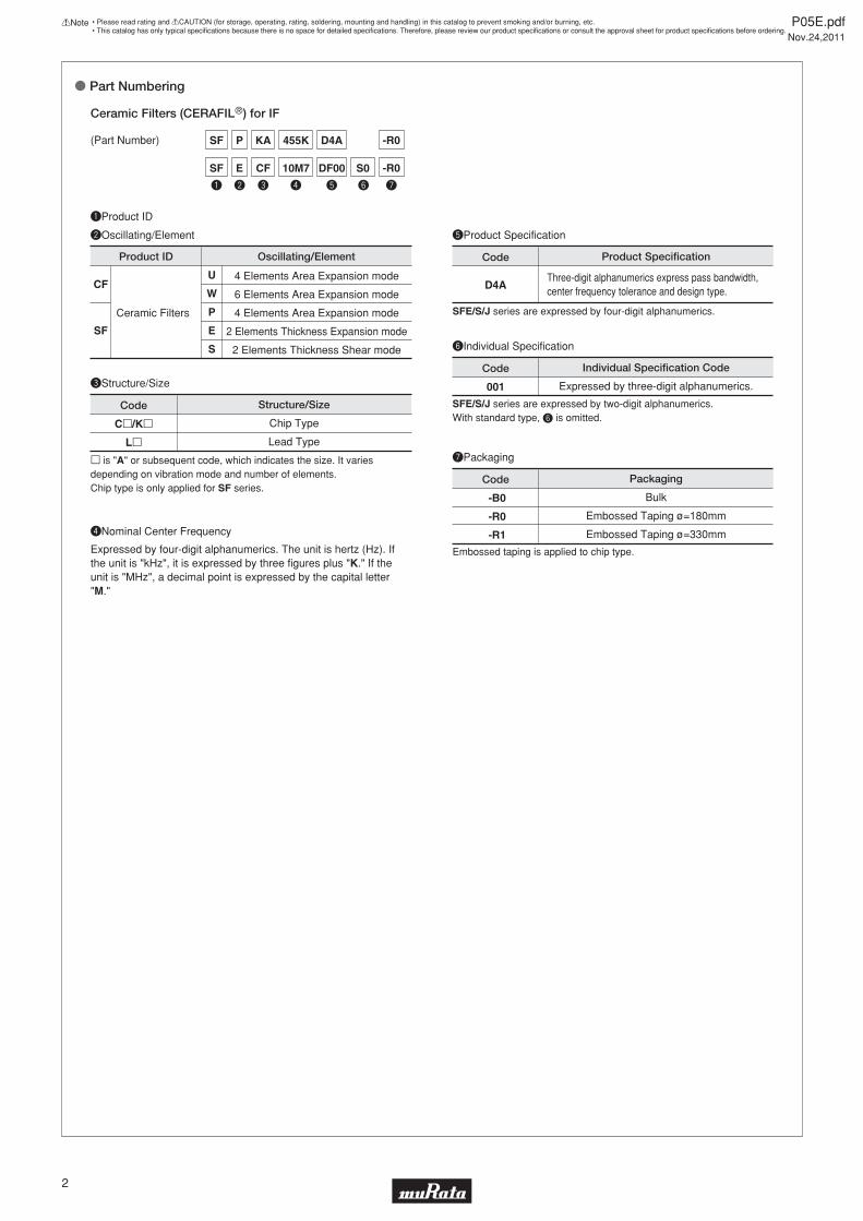
o Part Numbering
yew r t uq
KAP 455K D4A -R0SF
S0CFE 10M7 DF00 -R0SF
(Part Number)
qProduct ID
wOscillating/Element
Ceramic Filters (CERAFILr) for IF
CF
SF
U
W
P
E
S
Ceramic Filters
Three-digit alphanumerics express pass bandwidth, center frequency tolerance and design type.
Product ID
tProduct Specification
D4A
Code Product Specification
rNominal Center Frequency
Expressed by four-digit alphanumerics. The unit is hertz (Hz). If the unit is "kHz", it is expressed by three figures plus "K." If the unit is "MHz", a decimal point is expressed by the capital letter "M."
p is "A" or subsequent code, which indicates the size. It varies depending on vibration mode and number of elements.Chip type is only applied for SF series.
Expressed by three-digit alphanumerics.
yIndividual Specification
001
Code Individual Specification Code
Bulk
Embossed Taping ø=180mm
Embossed Taping ø=330mm
uPackaging
-B0
-R0
-R1
Code Packaging
Oscillating/Element
Chip Type
Lead Type
eStructure/Size
Cp/Kp
Lp
Code Structure/Size
4 Elements Area Expansion mode
6 Elements Area Expansion mode
4 Elements Area Expansion mode
2 Elements Thickness Expansion mode
2 Elements Thickness Shear mode
Embossed taping is applied to chip type.
SFE/S/J series are expressed by four-digit alphanumerics.
SFE/S/J series are expressed by two-digit alphanumerics.With standard type, y is omitted.
!Note P05E.pdfNov.24,2011
• Please read rating and !CAUTION (for storage, operating, rating, soldering, mounting and handling) in this catalog to prevent smoking and/or burning, etc.• This catalog has only typical specifi cations because there is no space for detailed specifi cations. Therefore, please review our product specifi cations or consult the approval sheet for product specifi cations before ordering.
3
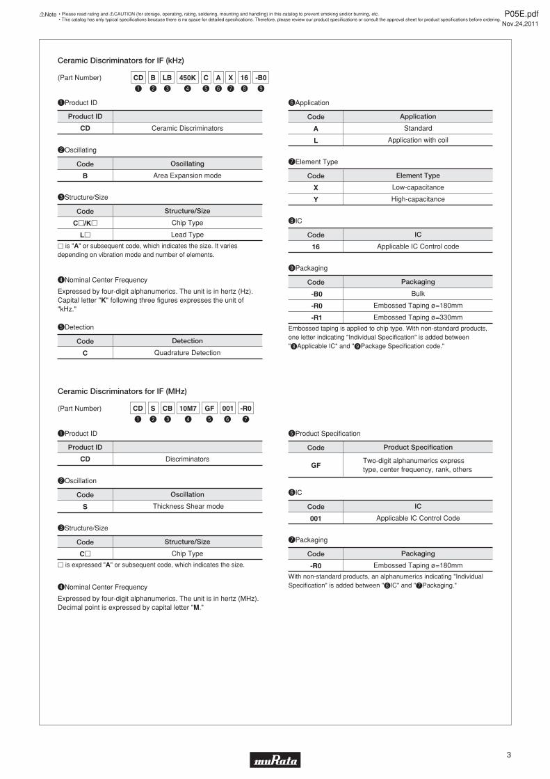
e
CB
w
S
r
10M7
t
GF
u
-R0
y
001
q
CD(Part Number)
qProduct ID
wOscillation
Ceramic Discriminators for IF (MHz)
CD Discriminators
Product ID
tProduct Specification
GF
Code Product Specification
With non-standard products, an alphanumerics indicating "Individual Specification" is added between "yIC" and "uPackaging."
eStructure/Size
Embossed Taping ø=180mm
yIC
001
Code IC
Applicable IC Control Code
uPackaging
-R0
Code Packaging
Thickness Shear modeS
Code Oscillation
Chip TypeCp
Code Structure/Size
p is expressed "A" or subsequent code, which indicates the size.
Two-digit alphanumerics expresstype, center frequency, rank, others
rNominal Center Frequency
Expressed by four-digit alphanumerics. The unit is in hertz (MHz).Decimal point is expressed by capital letter "M."
y
A
e
LB
w
B
r
450K
t
C
u
X
i
16
o
-B0
q
CD(Part Number)
qProduct ID
Ceramic Discriminators for IF (kHz)
CD Ceramic Discriminators
Quadrature Detection
Product ID
tDetection
C
Code Detection
Embossed taping is applied to chip type. With non-standard products, one letter indicating "Individual Specification" is added between "iApplicable IC" and "oPackage Specification code."
p is "A" or subsequent code, which indicates the size. It varies depending on vibration mode and number of elements.
Standard
Application with coil
yApplication
A
L
Code Application
Low-capacitance
High-capacitance
uElement Type
X
Y
Code Element Type
Applicable IC Control code
iIC
16
Code IC
Bulk
Embossed Taping ø=180mm
Embossed Taping ø=330mm
oPackaging
-B0
-R0
-R1
Code Packaging
Area Expansion mode
wOscillating
B
Code Oscillating
Chip Type
Lead Type
eStructure/Size
Cp/Kp
Lp
Code Structure/Size
rNominal Center Frequency
Expressed by four-digit alphanumerics. The unit is in hertz (Hz). Capital letter "K" following three figures expresses the unit of "kHz."
!Note P05E.pdfNov.24,2011
• Please read rating and !CAUTION (for storage, operating, rating, soldering, mounting and handling) in this catalog to prevent smoking and/or burning, etc.• This catalog has only typical specifi cations because there is no space for detailed specifi cations. Therefore, please review our product specifi cations or consult the approval sheet for product specifi cations before ordering.
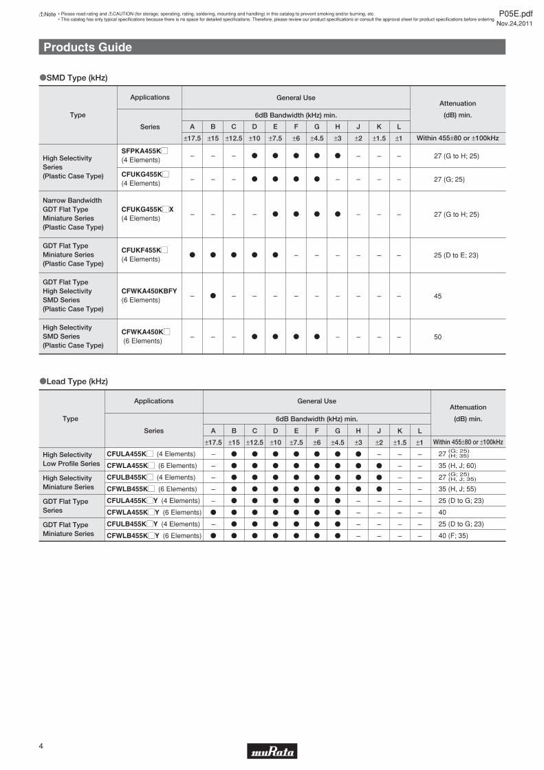
4
Type
Series
Applications
6dB Bandwidth (kHz) min.
General UseAttenuation
(dB) min.
oSMD Type (kHz)
High SelectivitySeries(Plastic Case Type)
Narrow BandwidthGDT Flat TypeMiniature Series(Plastic Case Type)
GDT Flat TypeMiniature Series(Plastic Case Type)
GDT Flat TypeHigh SelectivitySMD Series(Plastic Case Type)
High SelectivitySMD Series(Plastic Case Type)
SFPKA455KM
(4 Elements)
CFUKG455KM
(4 Elements)
CFUKG455KMX(4 Elements)
CFUKF455KM
(4 Elements)
CFWKA450KBFY(6 Elements)
CFWKA450KM (6 Elements)
oLead Type (kHz)
27 (G to H; 25)
27 (G; 25)
27 (G to H; 25)
25 (D to E; 23)
45
50
A
±17.5
–
–
–
o
–
–
B
±15
–
–
–
o
o
–
C
±12.5
–
–
–
o
–
–
D
±10
o
o
–
o
–
o
E
±7.5
o
o
o
o
–
o
F
±6
o
o
o
–
–
o
G
±4.5
o
o
o
–
–
o
H
±3
o
–
o
–
–
–
J
±2
–
–
–
–
–
–
K
±1.5
–
–
–
–
–
–
L
±1
–
–
–
–
–
–
Type
Series
Applications
6dB Bandwidth (kHz) min.
General UseAttenuation
(dB) min.
Within 455±80 or ±100kHz
Within 455±80 or ±100kHz
High SelectivityLow Profile Series
High SelectivityMiniature Series
GDT Flat TypeSeries
GDT Flat TypeMiniature Series
CFULA455KM (4 Elements)
CFWLA455KM (6 Elements)
CFULB455KM (4 Elements)
CFWLB455KM (6 Elements)
CFULA455KMY (4 Elements)
CFWLA455KMY (6 Elements)
CFULB455KMY (4 Elements)
CFWLB455KMY (6 Elements)
27
35 (H, J; 60)
27
35 (H, J; 55)
25 (D to G; 23)
40
25 (D to G; 23)
40 (F; 35)
A
±17.5
–
–
–
–
–
o
–
o
B
±15
o
o
o
o
o
o
o
o
C
±12.5
o
o
o
o
o
o
o
o
D
±10
o
o
o
o
o
o
o
o
E
±7.5
o
o
o
o
o
o
o
o
F
±6
o
o
o
o
o
o
o
o
G
±4.5
o
o
o
o
o
o
o
o
H
±3
o
o
o
o
–
–
–
–
J
±2
–
o
o
o
–
–
–
–
K
±1.5
–
–
–
–
–
–
–
–
L
±1
–
–
–
–
–
–
–
–
(G; 25)(H; 35)
(G; 25)(H, J; 35)
Products Guide
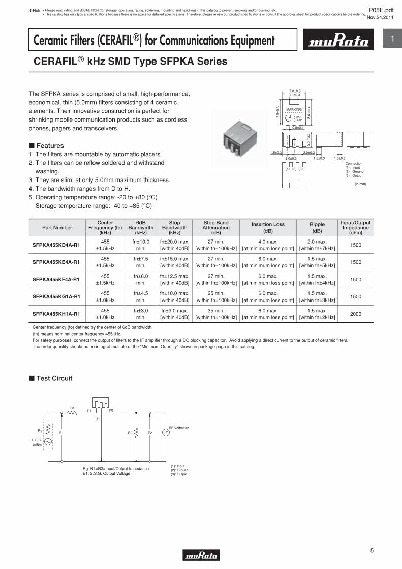
Ceramic Filters (CERAFILr) for Communications EquipmentCERAFILr kHz SMD Type SFPKA Series
The SFPKA series is comprised of small, high-performance, economical, thin (5.0mm) fi lters consisting of 4 ceramic elements. Their innovative construction is perfect for shrinking mobile communication products such as cordless phones, pagers and transceivers.
c Features1. The fi lters are mountable by automatic placers.2. The fi lters can be refl ow soldered and withstand washing.3. They are slim, at only 5.0mm maximum thickness.4. The bandwidth ranges from D to H.5. Operating temperature range: -20 to +80 (°C) Storage temperature range: -40 to +85 (°C)
7.5±
0.3
5.0
max
.
3.0±0.3
8.4
max
.
2.0±0.3
1.5±0.3
7.0±0.3
0.9±0.1
MARKING
EIAJCODE
2.0±0.3
(1) (2) (3)
1.5±0.3 1.6±0.3
Connection(1): Input(2): Ground(3): Output
(in mm)
Part NumberCenter
Frequency (fo)(kHz)
6dBBandwidth
(kHz)
StopBandwidth
(kHz)
Stop BandAttenuation
(dB)
Insertion Loss(dB)
Ripple(dB)
Input/OutputImpedance
(ohm)
SFPKA455KD4A-R1455
±1.5kHzfn±10.0
min.fn±20.0 max.[within 40dB]
27 min.[within fn±100kHz]
4.0 max.[at minimum loss point]
2.0 max.[within fn±7kHz]
1500
SFPKA455KE4A-R1455
±1.5kHzfn±7.5min.
fn±15.0 max.[within 40dB]
27 min.[within fn±100kHz]
6.0 max.[at minimum loss point]
1.5 max.[within fn±5kHz]
1500
SFPKA455KF4A-R1455
±1.5kHzfn±6.0min.
fn±12.5 max.[within 40dB]
27 min.[within fn±100kHz]
6.0 max.[at minimum loss point]
1.5 max.[within fn±4kHz]
1500
SFPKA455KG1A-R1455
±1.0kHzfn±4.5min.
fn±10.0 max.[within 40dB]
25 min.[within fn±100kHz]
6.0 max.[at minimum loss point]
1.5 max.[within fn±3kHz]
1500
SFPKA455KH1A-R1455
±1.0kHzfn±3.0min.
fn±9.0 max.[within 40dB]
35 min.[within fn±100kHz]
6.0 max.[at minimum loss point]
1.5 max.[within fn±2kHz]
2000
Center frequency (fo) defi ned by the center of 6dB bandwidth.
(fn) means nominal center frequency 455kHz.
For safety purposes, connect the output of fi lters to the IF amplifi er through a DC blocking capacitor. Avoid applying a direct current to the output of ceramic fi lters.
The order quantity should be an integral multiple of the "Minimum Quantity" shown in package page in this catalog.
Rg+R1=R2=Input/Output ImpedanceE1: S.S.G. Output Voltage
E1
R1
Rg
S.S.G.0dBm
(1)
(2)
(3)
R2 E2
RF Voltmeter
(1): Input (2): Ground (3): Output
c Test Circuit
P05E.pdfNov.24,2011
5
!Note • Please read rating and !CAUTION (for storage, operating, rating, soldering, mounting and handling) in this catalog to prevent smoking and/or burning, etc.• This catalog has only typical specifi cations because there is no space for detailed specifi cations. Therefore, please review our product specifi cations or consult the approval sheet for product specifi cations before ordering.
1
100
40
30
20
10
0A
ttenu
atio
n (d
B)
G.D
.T. (
μsec
.)
430 455 480
Frequency (kHz)
90
80
70
60
50
0
240
280
320
360
400
40
80
120
160
200
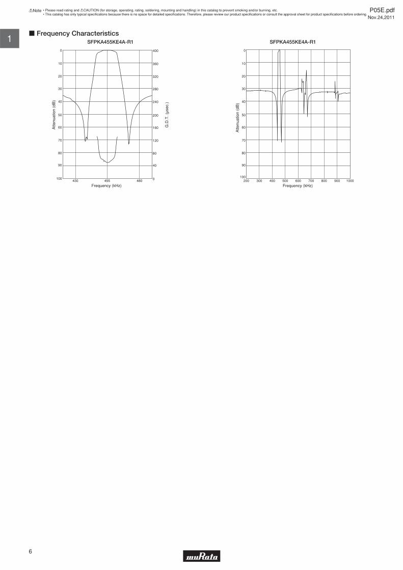
c Frequency CharacteristicsSFPKA455KE4A-R1
100
40
30
20
10
0
Atte
nuat
ion
(dB
)
200
Frequency (kHz)
90
80
70
60
50
300 400 500 600 700 800 900 1000
SFPKA455KE4A-R1
P05E.pdfNov.24,2011
6
!Note • Please read rating and !CAUTION (for storage, operating, rating, soldering, mounting and handling) in this catalog to prevent smoking and/or burning, etc.• This catalog has only typical specifi cations because there is no space for detailed specifi cations. Therefore, please review our product specifi cations or consult the approval sheet for product specifi cations before ordering.
1
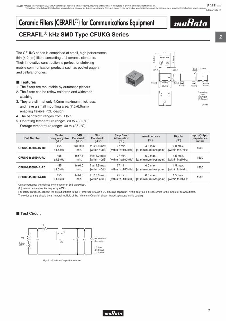
Ceramic Filters (CERAFILr) for Communications EquipmentCERAFILr kHz SMD Type CFUKG Series
The CFUKG series is comprised of small, high-performance,thin (4.0mm) fi lters consisting of 4 ceramic elements.Their innovative construction is perfect for shrinkingmobile communication products such as pocket pagers and cellular phones.
c Features1. The fi lters are mountable by automatic placers.2. The fi lters can be refl ow soldered and withstand washing.3. They are slim, at only 4.0mm maximum thickness, and have a small mounting area (7.5x6.0mm) enabling fl exible PCB design.4. The bandwidth ranges from D to G.5. Operating temperature range: -20 to +80 (°C) Storage temperature range: -40 to +85 (°C)
1.5±0.3 3.0±0.3
1.0±0.1
4.0±0.3
6.5±
0.3
7.5
max
.
C0.5 1.2±0.1
4.0
max
.
1.0±0.1
(in mm)
Connection(1): Input(2): Output(3): Ground
1.0±0.3 1.0±0.31.5±0.36.0±0.3
(1) (2)
(3)
MARKING
EIAJCODE
Part NumberCenter
Frequency (fo)(kHz)
6dBBandwidth
(kHz)
StopBandwidth
(kHz)
Stop BandAttenuation
(dB)
Insertion Loss(dB)
Ripple(dB)
Input/OutputImpedance
(ohm)
CFUKG455KD4A-R0455
±1.5kHzfn±10.0
min.fn±20.0 max.[within 40dB]
27 min.[within fn±100kHz]
4.0 max.[at minimum loss point]
2.0 max.[within fn±7kHz]
1500
CFUKG455KE4A-R0455
±1.5kHzfn±7.5min.
fn±15.0 max.[within 40dB]
27 min.[within fn±100kHz]
6.0 max.[at minimum loss point]
1.5 max.[within fn±5kHz]
1500
CFUKG455KF4A-R0455
±1.5kHzfn±6.0min.
fn±12.5 max.[within 40dB]
27 min.[within fn±100kHz]
6.0 max.[at minimum loss point]
1.5 max.[within fn±4kHz]
1500
CFUKG455KG1A-R0455
±1.0kHzfn±4.5min.
fn±10.0 max.[within 40dB]
25 min.[within fn±100kHz]
6.0 max.[at minimum loss point]
1.5 max.[within fn±3kHz]
1500
Center frequency (fo) defi ned by the center of 6dB bandwidth.
(fn) means nominal center frequency 455kHz.
For safety purposes, connect the output of fi lters to the IF amplifi er through a DC blocking capacitor. Avoid applying a direct current to the output of ceramic fi lters.
The order quantity should be an integral multiple of the "Minimum Quantity" shown in package page in this catalog.
E1Rg
S.S.G.0dBm
R1
RF Voltmeter Connection
(1): Input (2): Output (3): Ground
(2)
(3)
(1)
R2 E2
Rg+R1=R2=Input/Output Impedance
c Test Circuit
P05E.pdfNov.24,2011
7
!Note • Please read rating and !CAUTION (for storage, operating, rating, soldering, mounting and handling) in this catalog to prevent smoking and/or burning, etc.• This catalog has only typical specifi cations because there is no space for detailed specifi cations. Therefore, please review our product specifi cations or consult the approval sheet for product specifi cations before ordering.
2
100
40
30
20
10
0A
ttenu
atio
n (d
B)
0
100
200
300
400
G.D
.T. (
μsec
.)
430 455 480
Frequency (kHz)
90
80
70
60
50
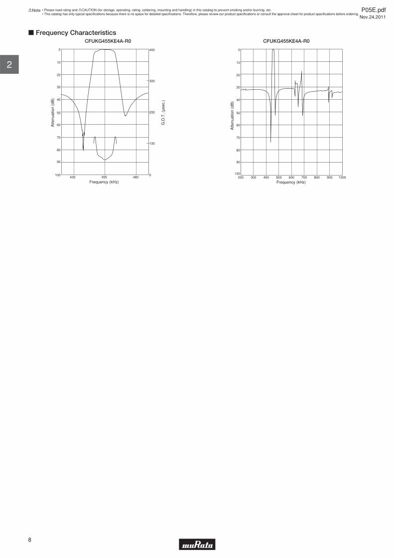
c Frequency CharacteristicsCFUKG455KE4A-R0
100
40
30
20
10
0
Atte
nuat
ion
(dB
)
200
Frequency (kHz)
90
80
70
60
50
300 400 500 600 700 800 900 1000
CFUKG455KE4A-R0
P05E.pdfNov.24,2011
8
!Note • Please read rating and !CAUTION (for storage, operating, rating, soldering, mounting and handling) in this catalog to prevent smoking and/or burning, etc.• This catalog has only typical specifi cations because there is no space for detailed specifi cations. Therefore, please review our product specifi cations or consult the approval sheet for product specifi cations before ordering.
2
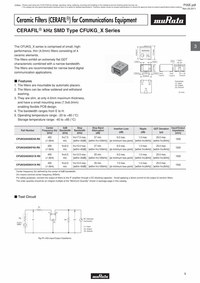
Ceramic Filters (CERAFILr) for Communications EquipmentCERAFILr kHz SMD Type CFUKG_X Series
The CFUKG_X series is comprised of small, high-performance, thin (4.0mm) fi lters consisting of 4 ceramic elements.The fi lters exhibit an extremely fl at GDT characteristic combined with a narrow bandwidth.The fi lters are recommended for narrow band digitalcommunication applications.
c Features1. The fi lters are mountable by automatic placers.2. The fi lters can be refl ow soldered and withstand washing.3. They are slim, at only 4.0mm maximum thickness, and have a small mounting area (7.5x6.0mm) enabling fl exible PCB design.4. The bandwidth ranges from E to H. 5. Operating temperature range: -20 to +80 (°C) Storage temperature range: -40 to +85 (°C)
1.5±0.3 3.0±0.3
1.0±0.1
4.0±0.3
6.5±
0.3
7.5
max
.
C0.5 1.2±0.1
4.0
max
.
1.0±0.1
(in mm)
Connection(1): Input(2): Output(3): Ground
1.0±0.3 1.0±0.31.5±0.36.0±0.3
(1) (2)
(3)
MARKING
EIAJCODE
Part NumberCenter
Frequency (fo)(kHz)
6dBBandwidth
(kHz)
StopBandwidth
(kHz)
Stop BandAttenuation
(dB)
Insertion Loss(dB)
Ripple(dB)
GDT Deviation(µs)
Input/OutputImpedance
(ohm)
CFUKG455KE4X-R0455
±1.5kHzfn±7.5min.
fn±17.5 max.[within 40dB]
27 min.[within fn±100kHz]
6.0 max.[at minimum loss point]
1.0 max.[within fn±5kHz]
25.0 max.[within fn±5kHz]
1500
CFUKG455KF4X-R0455
±1.5kHzfn±6.0min.
fn±15.0 max.[within 40dB]
27 min.[within fn±100kHz]
6.0 max.[at minimum loss point]
1.0 max.[within fn±4kHz]
25.0 max.[within fn±4kHz]
1500
CFUKG455KG1X-R0455
±1.0kHzfn±4.5min.
fn±12.5 max.[within 40dB]
25 min.[within fn±100kHz]
6.0 max.[at minimum loss point]
1.0 max.[within fn±3kHz]
25.0 max.[within fn±3kHz]
1500
CFUKG455KH1X-R0455
±1.0kHzfn±3.0min.
fn±10.0 max.[within 40dB]
25 min.[within fn±100kHz]
7.0 max.[at minimum loss point]
1.0 max.[within fn±2kHz]
25.0 max.[within fn±2kHz]
1500
Center frequency (fo) defi ned by the center of 6dB bandwidth.
(fn) means nominal center frequency 455kHz.
For safety purposes, connect the output of fi lters to the IF amplifi er through a DC blocking capacitor. Avoid applying a direct current to the output of ceramic fi lters.
The order quantity should be an integral multiple of the "Minimum Quantity" shown in package page in this catalog.
E1Rg
S.S.G.0dBm
R1
RF Voltmeter Connection
(1): Input (2): Output (3): Ground
(2)
(3)
(1)
R2 E2
Rg+R1=R2=Input/Output Impedance
c Test Circuit
P05E.pdfNov.24,2011
9
!Note • Please read rating and !CAUTION (for storage, operating, rating, soldering, mounting and handling) in this catalog to prevent smoking and/or burning, etc.• This catalog has only typical specifi cations because there is no space for detailed specifi cations. Therefore, please review our product specifi cations or consult the approval sheet for product specifi cations before ordering.
3
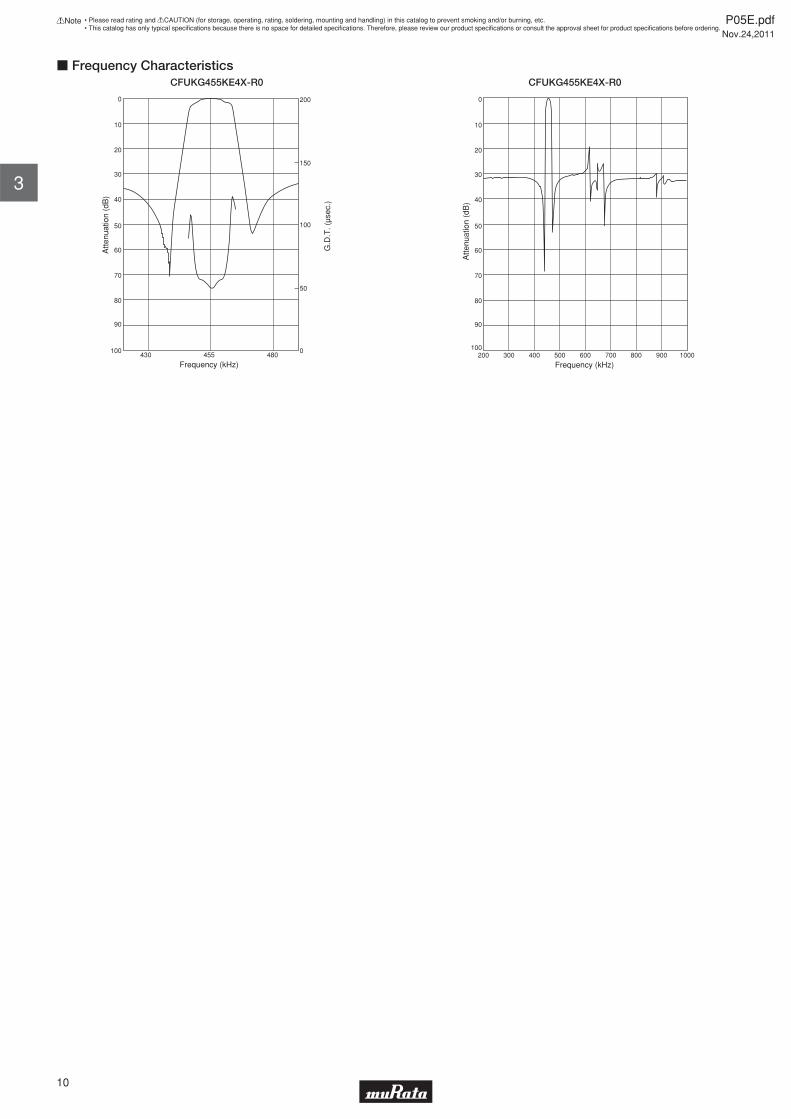
100
40
30
20
10
0A
ttenu
atio
n (d
B)
0
50
100
150
200
G.D
.T. (
μsec
.)
430 455 480
Frequency (kHz)
90
80
70
60
50
c Frequency CharacteristicsCFUKG455KE4X-R0
100
40
30
20
10
0
Atte
nuat
ion
(dB
)
200
Frequency (kHz)
90
80
70
60
50
300 400 500 600 700 800 900 1000
CFUKG455KE4X-R0
P05E.pdfNov.24,2011
10
!Note • Please read rating and !CAUTION (for storage, operating, rating, soldering, mounting and handling) in this catalog to prevent smoking and/or burning, etc.• This catalog has only typical specifi cations because there is no space for detailed specifi cations. Therefore, please review our product specifi cations or consult the approval sheet for product specifi cations before ordering.
3
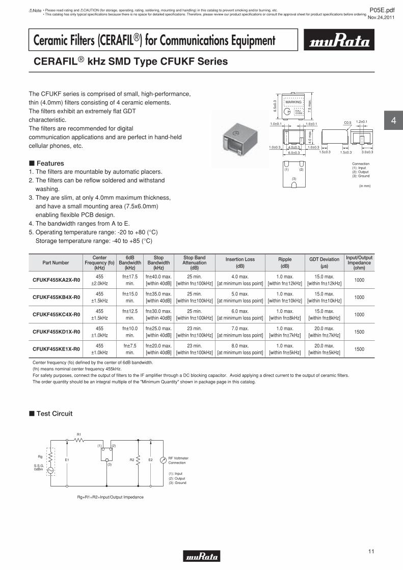
Ceramic Filters (CERAFILr) for Communications EquipmentCERAFILr kHz SMD Type CFUKF Series
The CFUKF series is comprised of small, high-performance, thin (4.0mm) fi lters consisting of 4 ceramic elements.The fi lters exhibit an extremely fl at GDT characteristic.The fi lters are recommended for digital communication applications and are perfect in hand-held cellular phones, etc.
c Features1. The fi lters are mountable by automatic placers.2. The fi lters can be refl ow soldered and withstand washing.3. They are slim, at only 4.0mm maximum thickness, and have a small mounting area (7.5x6.0mm) enabling fl exible PCB design.4. The bandwidth ranges from A to E.5. Operating temperature range: -20 to +80 (°C) Storage temperature range: -40 to +85 (°C)
1.5±0.3 3.0±0.3
1.0±0.1
4.0±0.3
6.5±
0.3
7.5
max
.
C0.5 1.2±0.1
4.0
max
.
1.0±0.1
(in mm)
Connection(1): Input(2): Output(3): Ground
1.0±0.3 1.0±0.31.5±0.36.0±0.3
(1) (2)
(3)
MARKING
EIAJCODE
Part NumberCenter
Frequency (fo)(kHz)
6dBBandwidth
(kHz)
StopBandwidth
(kHz)
Stop BandAttenuation
(dB)
Insertion Loss(dB)
Ripple(dB)
GDT Deviation(µs)
Input/OutputImpedance
(ohm)
CFUKF455KA2X-R0455
±2.0kHzfn±17.5
min.fn±40.0 max.[within 40dB]
25 min.[within fn±100kHz]
4.0 max.[at minimum loss point]
1.0 max.[within fn±12kHz]
15.0 max.[within fn±12kHz]
1000
CFUKF455KB4X-R0455
±1.5kHzfn±15.0
min.fn±35.0 max.[within 40dB]
25 min.[within fn±100kHz]
5.0 max.[at minimum loss point]
1.0 max.[within fn±10kHz]
15.0 max.[within fn±10kHz]
1000
CFUKF455KC4X-R0455
±1.5kHzfn±12.5
min.fn±30.0 max.[within 40dB]
25 min.[within fn±100kHz]
6.0 max.[at minimum loss point]
1.0 max.[within fn±8kHz]
15.0 max.[within fn±8kHz]
1000
CFUKF455KD1X-R0455
±1.0kHzfn±10.0
min.fn±25.0 max.[within 40dB]
23 min.[within fn±100kHz]
7.0 max.[at minimum loss point]
1.0 max.[within fn±7kHz]
20.0 max.[within fn±7kHz]
1500
CFUKF455KE1X-R0455
±1.0kHzfn±7.5min.
fn±20.0 max.[within 40dB]
23 min.[within fn±100kHz]
8.0 max.[at minimum loss point]
1.0 max.[within fn±5kHz]
20.0 max.[within fn±5kHz]
1500
Center frequency (fo) defi ned by the center of 6dB bandwidth.
(fn) means nominal center frequency 455kHz.
For safety purposes, connect the output of fi lters to the IF amplifi er through a DC blocking capacitor. Avoid applying a direct current to the output of ceramic fi lters.
The order quantity should be an integral multiple of the "Minimum Quantity" shown in package page in this catalog.
E1Rg
S.S.G.0dBm
R1
RF Voltmeter Connection
(1): Input (2): Output (3): Ground
(2)
(3)
(1)
R2 E2
Rg+R1=R2=Input/Output Impedance
c Test Circuit
P05E.pdfNov.24,2011
11
!Note • Please read rating and !CAUTION (for storage, operating, rating, soldering, mounting and handling) in this catalog to prevent smoking and/or burning, etc.• This catalog has only typical specifi cations because there is no space for detailed specifi cations. Therefore, please review our product specifi cations or consult the approval sheet for product specifi cations before ordering.
4
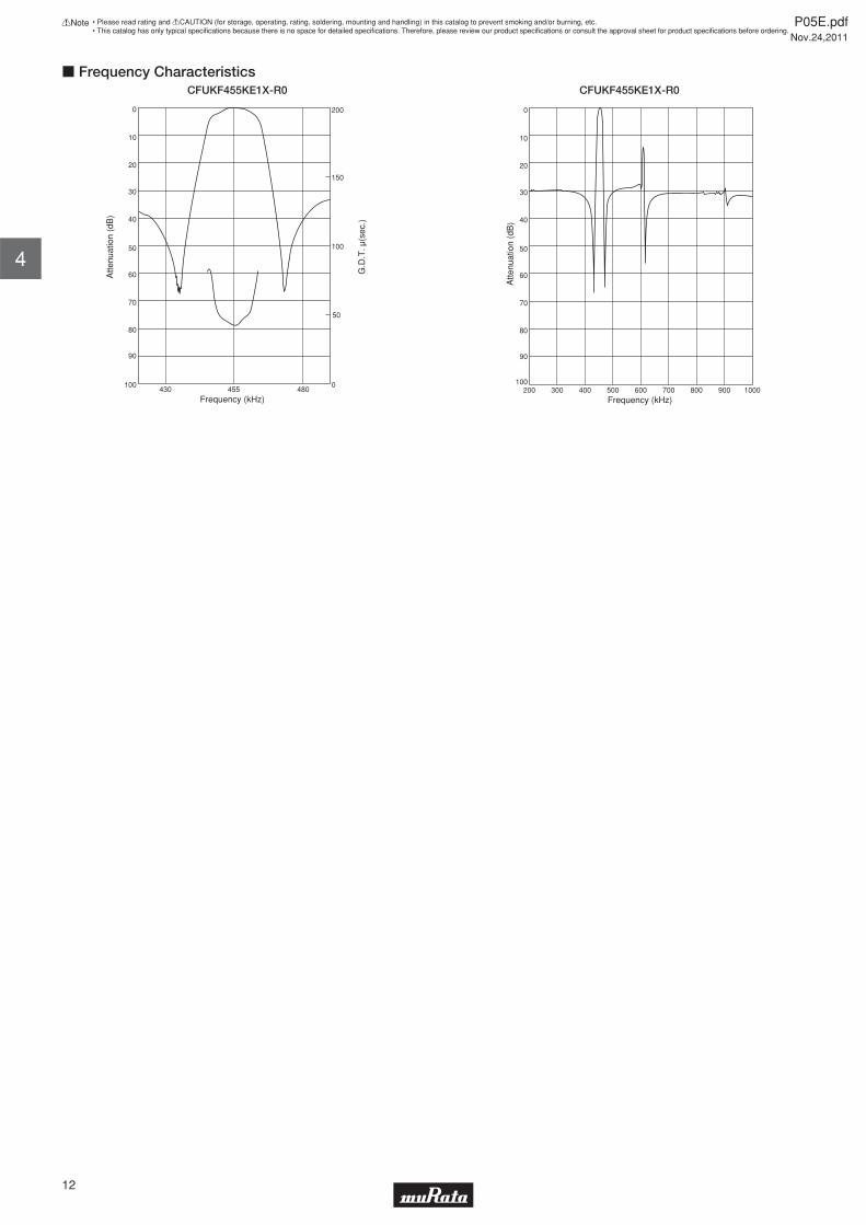
100
40
30
20
10
0A
ttenu
atio
n (d
B)
0
50
100
150
200
G.D
.T. μ
(sec
.)
430 455 480Frequency (kHz)
90
80
70
60
50
c Frequency CharacteristicsCFUKF455KE1X-R0
100
40
30
20
10
0
Atte
nuat
ion
(dB
)
200Frequency (kHz)
90
80
70
60
50
300 400 500 600 700 800 900 1000
CFUKF455KE1X-R0
P05E.pdfNov.24,2011
12
!Note • Please read rating and !CAUTION (for storage, operating, rating, soldering, mounting and handling) in this catalog to prevent smoking and/or burning, etc.• This catalog has only typical specifi cations because there is no space for detailed specifi cations. Therefore, please review our product specifi cations or consult the approval sheet for product specifi cations before ordering.
4
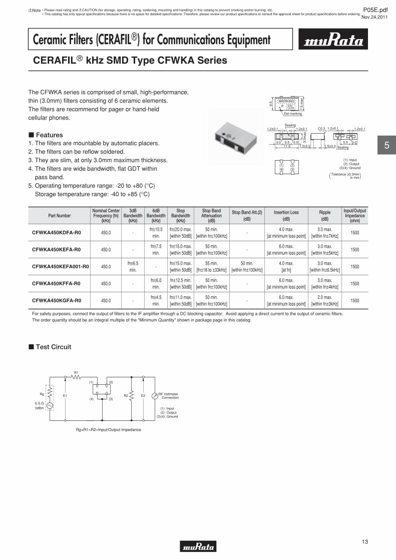
Ceramic Filters (CERAFILr) for Communications EquipmentCERAFILr kHz SMD Type CFWKA Series
The CFWKA series is comprised of small, high-performance,thin (3.0mm) fi lters consisting of 6 ceramic elements.The fi lters are recommend for pager or hand-heldcellular phones.
c Features1. The fi lters are mountable by automatic placers.2. The fi lters can be refl ow soldered.3. They are slim, at only 3.0mm maximum thickness.4. The fi lters are wide bandwidth, fl at GDT within pass band.5. Operating temperature range: -20 to +80 (°C) Storage temperature range: -40 to +85 (°C)
MARKING
6.5
7.5
max
.3.
0max
.
11.55.5 3.0
1.2±0.1
1.5±0.3
1.2±0.1 1.2±0.1
1.5±0.3
1.2±0.1 C0.3
3.03.0 5.5
Dot marking
Sealing
Sealing
: Input: Output: Ground
(1)
(1)(2)
(3)(4)(2)
(4) (3)
EIAJCODE
Tolerance ±0.3mmin mm( )
Part NumberNominal CenterFrequency (fn)
(kHz)
3dBBandwidth
(kHz)
6dBBandwidth
(kHz)
StopBandwidth
(kHz)
Stop BandAttenuation
(dB)
Stop Band Att.(2)(dB)
Insertion Loss(dB)
Ripple(dB)
Input/OutputImpedance
(ohm)
CFWKA450KDFA-R0 450.0 -fn±10.0
min.fn±20.0 max.[within 50dB]
50 min.[within fn±100kHz]
-4.0 max.
[at minimum loss point]3.0 max.
[within fn±7kHz]1500
CFWKA450KEFA-R0 450.0 -fn±7.5min.
fn±15.0 max.[within 50dB]
50 min.[within fn±100kHz]
-6.0 max.
[at minimum loss point]3.0 max.
[within fn±5kHz]1500
CFWKA450KEFA001-R0 450.0fn±6.5min.
-fn±15.0 max.[within 50dB]
55 min.[fn±18 to ±33kHz]
50 min.[within fn±100kHz]
4.0 max.[at fn]
3.0 max.[within fn±6.5kHz]
1500
CFWKA450KFFA-R0 450.0 -fn±6.0min.
fn±12.5 min.[within 50dB]
50 min.[within fn±100kHz]
-6.0 max.
[at minimum loss point]3.0 max.
[within fn±4kHz]1500
CFWKA450KGFA-R0 450.0 -fn±4.5min.
fn±11.0 max.[within 50dB]
50 min.[within fn±100kHz]
-6.0 max.
[at minimum loss point]2.0 max.
[within fn±3kHz]1500
For safety purposes, connect the output of fi lters to the IF amplifi er through a DC blocking capacitor. Avoid applying a direct current to the output of ceramic fi lters.
The order quantity should be an integral multiple of the "Minimum Quantity" shown in package page in this catalog.
E1Rg
S.S.G.0dBm
R1
RF Voltmeter Connection
(1): Input (2): Output(3)(4): Ground
(2)
(4)
(1)
R2 E2(3)
Rg+R1=R2=Input/Output Impedance
c Test Circuit
P05E.pdfNov.24,2011
13
!Note • Please read rating and !CAUTION (for storage, operating, rating, soldering, mounting and handling) in this catalog to prevent smoking and/or burning, etc.• This catalog has only typical specifi cations because there is no space for detailed specifi cations. Therefore, please review our product specifi cations or consult the approval sheet for product specifi cations before ordering.
5
Frequency (kHz)
Atte
nuat
ion
(dB
)
G.D
.T. (
μ se
c.)
400
300
200
100
0440.0 450.0 460.0
0
4
8
12
16
20
24
28
32
36
40
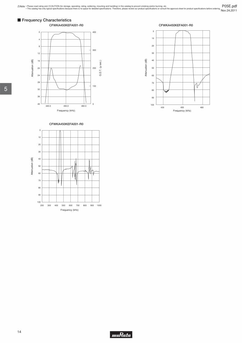
c Frequency CharacteristicsCFWKA450KEFA001-R0
10
0
20
30
40
50
60
70
80
90
100430 455 480
Frequency (kHz)
Atte
nuat
ion
(dB
)
CFWKA450KEFA001-R0
Frequency (kHz)
Atte
nuat
ion
(dB
)
200 300 400 500 600 700 800 900 1000
0
10
20
30
40
50
60
70
80
90
100
CFWKA450KEFA001-R0
P05E.pdfNov.24,2011
14
!Note • Please read rating and !CAUTION (for storage, operating, rating, soldering, mounting and handling) in this catalog to prevent smoking and/or burning, etc.• This catalog has only typical specifi cations because there is no space for detailed specifi cations. Therefore, please review our product specifi cations or consult the approval sheet for product specifi cations before ordering.
5
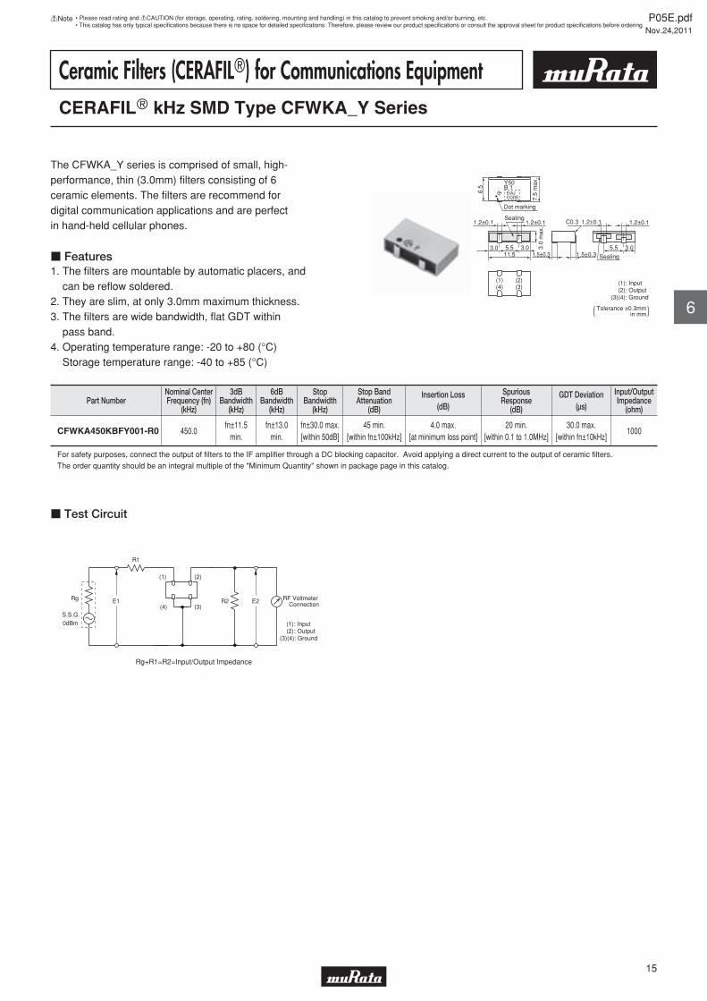
Ceramic Filters (CERAFILr) for Communications EquipmentCERAFILr kHz SMD Type CFWKA_Y Series
The CFWKA_Y series is comprised of small, high-performance, thin (3.0mm) fi lters consisting of 6 ceramic elements. The fi lters are recommend for digital communication applications and are perfect in hand-held cellular phones.
c Features1. The fi lters are mountable by automatic placers, and can be refl ow soldered.2. They are slim, at only 3.0mm maximum thickness.3. The fi lters are wide bandwidth, fl at GDT within pass band.4. Operating temperature range: -20 to +80 (°C) Storage temperature range: -40 to +85 (°C)
Y50B 1
6.5
7.5
max
.3.
0 m
ax.
11.55.5 3.0
1.2±0.1
1.5±0.3
1.2±0.1 1.2±0.1
1.5±0.3
1.2±0.1 C0.3
3.03.0 5.5
Dot marking
Sealing
Sealing
Tolerance ±0.3mmin mm
: Input: Output: Ground
(1) (2)(4) (3)
EIAJCODE
( )
(1)(2)
(3)(4)
Part NumberNominal CenterFrequency (fn)
(kHz)
3dBBandwidth
(kHz)
6dBBandwidth
(kHz)
StopBandwidth
(kHz)
Stop BandAttenuation
(dB)
Insertion Loss(dB)
SpuriousResponse
(dB)
GDT Deviation(µs)
Input/OutputImpedance
(ohm)
CFWKA450KBFY001-R0 450.0fn±11.5
min.fn±13.0
min.fn±30.0 max.[within 50dB]
45 min.[within fn±100kHz]
4.0 max.[at minimum loss point]
20 min.[within 0.1 to 1.0MHz]
30.0 max.[within fn±10kHz]
1000
For safety purposes, connect the output of fi lters to the IF amplifi er through a DC blocking capacitor. Avoid applying a direct current to the output of ceramic fi lters.
The order quantity should be an integral multiple of the "Minimum Quantity" shown in package page in this catalog.
E1Rg
S.S.G.0dBm
R1
RF Voltmeter Connection
(1): Input (2): Output(3)(4): Ground
(2)
(4)
(1)
R2 E2(3)
Rg+R1=R2=Input/Output Impedance
c Test Circuit
P05E.pdfNov.24,2011
15
!Note • Please read rating and !CAUTION (for storage, operating, rating, soldering, mounting and handling) in this catalog to prevent smoking and/or burning, etc.• This catalog has only typical specifi cations because there is no space for detailed specifi cations. Therefore, please review our product specifi cations or consult the approval sheet for product specifi cations before ordering.
6
Atte
nuat
ion
(dB
)
G.D
.T. (
μ se
c.)
200
150
100
50
0420 430 440 450 460 470 480
Frequency (kHz)
0
2
4
6
8
10
12
14
16
18
20
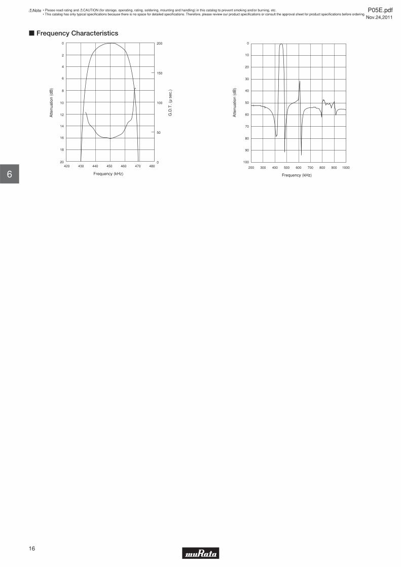
c Frequency Characteristics
Frequency (kHz)
Atte
nuat
ion
(dB
)
200 300 400 500 600 700 800 900 1000
0
10
20
30
40
50
60
70
80
90
100
P05E.pdfNov.24,2011
16
!Note • Please read rating and !CAUTION (for storage, operating, rating, soldering, mounting and handling) in this catalog to prevent smoking and/or burning, etc.• This catalog has only typical specifi cations because there is no space for detailed specifi cations. Therefore, please review our product specifi cations or consult the approval sheet for product specifi cations before ordering.
6
kHz SMD Type CERAFILr Notice
Continued on the following page.
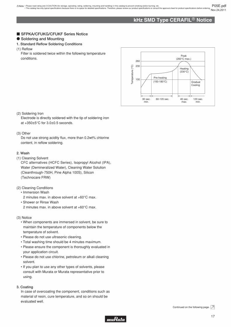
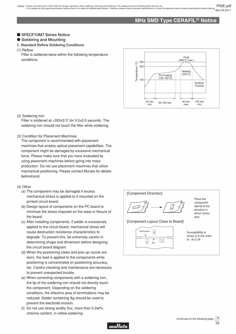
Filter is soldered twice within the following temperature conditions.
1. Standard Reflow Soldering Conditions
2. Wash
(1) Reflow
Electrode is directly soldered with the tip of soldering iron at +350±5°C for 3.0±0.5 seconds.
(2) Soldering Iron
Do not use strong acidity flux, more than 0.2wt% chlorine content, in reflow soldering.
(3) Other
2 minutes max. in above solvent at +60°C max.
2 minutes max. in above solvent at +60°C max.
CFC alternatives (HCFC Series), Isopropyl Alcohol (IPA),
(Cleanthrough-750H, Pine Alpha 100S), Silicon
3. CoatingIn case of overcoating the component, conditions such as material of resin, cure temperature, and so on should be evaluated well.
(1) Cleaning Solvent
(2) Cleaning Conditions
maintain the temperature of components below the temperature of solvent.
your application circuit.
solvent.
consult with Murata or Murata representative prior to using.
(3) Notice
o Soldering and Mounting
(260°C max.)
Heating(230°C)
GradualCooling
Pre-heating
(150-180°C)100
230
260
Tem
pera
ture
(°C
)
60-120 sec.max.
30 sec.min.
120 sec.min.
c SFPKA/CFUKG/CFUKF Series Notice
P05E.pdfNov.24,2011
17
!Note • Please read rating and !CAUTION (for storage, operating, rating, soldering, mounting and handling) in this catalog to prevent smoking and/or burning, etc.• This catalog has only typical specifi cations because there is no space for detailed specifi cations. Therefore, please review our product specifi cations or consult the approval sheet for product specifi cations before ordering.
kHz SMD Type CERAFILr Notice
o Storage and Operating Conditions
o RatingThe component may be damaged if excessive mechanical stress is applied.
o Handling1. If the component is cleaned, please confirm that the
reliability has not been degraded. 2. The components, packed in a moisture-proof bag (dry
pack), are sensitive to moisture. The following treatment is required before applying reflow soldering, to avoid package cracks or reliability degradation caused by thermal stress. When unpacked, store the component in an atmosphere of below 25°C and below 65%R.H., and solder within 48 hours.
3. For safety purposes, connect the output of filters to the IF amplifier through a D.C. blocking capacitor. Avoid applying a direct current to the output of ceramic filters.
1. Product Storage ConditionPlease store the products in a room where the temperature/humidity is stable, and avoid such places where there are large temperature changes. Please store the products under the following conditions: Temperature: -10 to +40°CHumidity: 15 to 85% R.H.
2. Expiration Date on StorageExpiration date (shelf life) of the products is six months after delivery under the conditions of a sealed and unopened package. Please use the products within six months after delivery. If you store the products for a long time (more than six months), use carefully because solderability may be degraded due to storage under poor conditions.Please confirm solderability and characteristics for the products regularly.
3. Notice on Product Storage(1) Please do not store the products in a chemical
atmosphere (Acids, Alkali, Bases, Organic gas, Sulfides and so on), because the characteristics may be reduced in quality and may be degraded in solderability due to storage in a chemical atmosphere.
(2) Please do not put the products directly on the floor without anything under them to avoid damp places and/or dusty places.
(3) Please do not store the products in places such as a damp heated place or any place exposed to direct sunlight or excessive vibration.
(4) Please use the products immediately after the package is opened, because the characteristics may be reduced in quality and/or be degraded in solderability due to storage under poor condition.
(5) Please do not drop the products to avoid cracking of ceramic element.
4. OtherPlease be sure to consult with our sales representative or engineer whenever the products are to be used in conditions not listed above.
Continued from the preceding page.
P05E.pdfNov.24,2011
18
!Note • Please read rating and !CAUTION (for storage, operating, rating, soldering, mounting and handling) in this catalog to prevent smoking and/or burning, etc.• This catalog has only typical specifi cations because there is no space for detailed specifi cations. Therefore, please review our product specifi cations or consult the approval sheet for product specifi cations before ordering.
kHz SMD Type CERAFILr Notice
Continued on the following page.
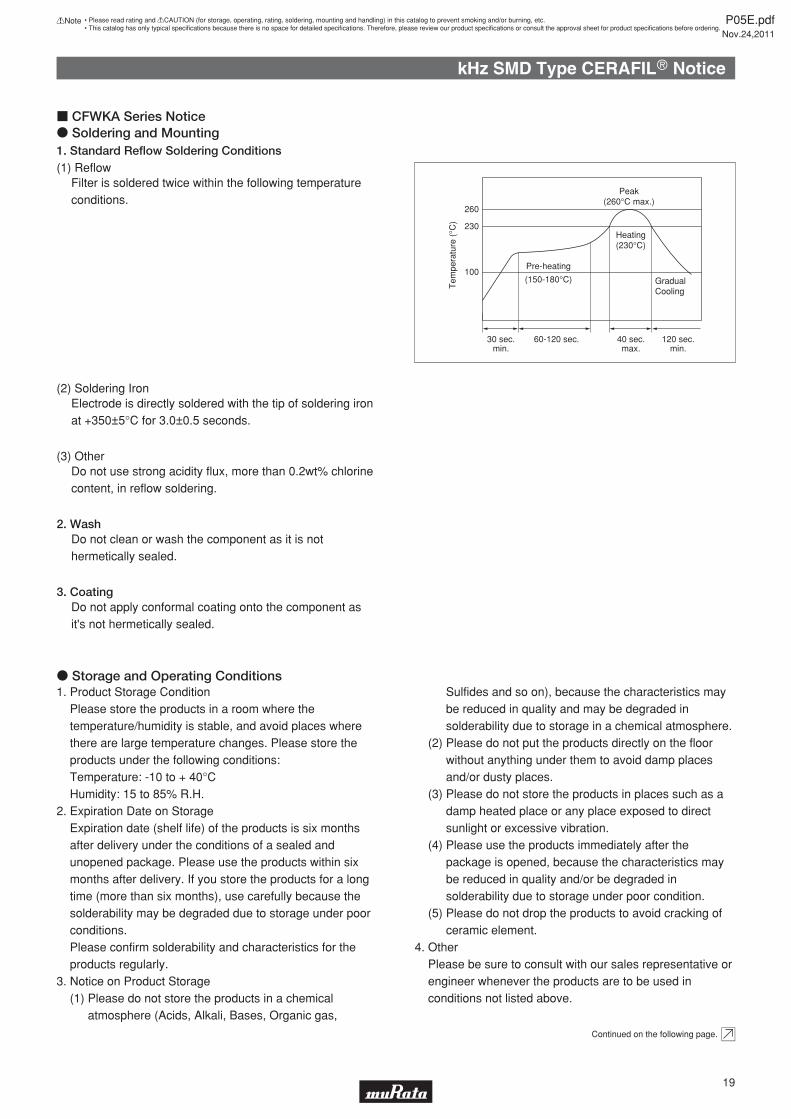
Filter is soldered twice within the following temperature conditions.
1. Standard Reflow Soldering Conditions(1) Reflow
Electrode is directly soldered with the tip of soldering iron at +350±5°C for 3.0±0.5 seconds.
(2) Soldering Iron
Do not use strong acidity flux, more than 0.2wt% chlorine content, in reflow soldering.
(3) Other
o Soldering and Mounting
Peak(260°C max.)
Heating(230°C)
GradualCooling
Pre-heating
(150-180°C)100
230
260
Tem
pera
ture
(°C
)
60-120 sec. 40 sec.max.
30 sec.min.
120 sec.min.
Do not clean or wash the component as it is not hermetically sealed.
2. Wash
Do not apply conformal coating onto the component as it's not hermetically sealed.
3. Coating
o Storage and Operating Conditions1. Product Storage Condition
Please store the products in a room where the temperature/humidity is stable, and avoid places where there are large temperature changes. Please store the products under the following conditions: Temperature: -10 to + 40°CHumidity: 15 to 85% R.H.
2. Expiration Date on StorageExpiration date (shelf life) of the products is six months after delivery under the conditions of a sealed and unopened package. Please use the products within six months after delivery. If you store the products for a long time (more than six months), use carefully because the solderability may be degraded due to storage under poor conditions. Please confirm solderability and characteristics for the products regularly.
3. Notice on Product Storage(1) Please do not store the products in a chemical
atmosphere (Acids, Alkali, Bases, Organic gas,
Sulfides and so on), because the characteristics may be reduced in quality and may be degraded in solderability due to storage in a chemical atmosphere.
(2) Please do not put the products directly on the floor without anything under them to avoid damp places and/or dusty places.
(3) Please do not store the products in places such as a damp heated place or any place exposed to direct sunlight or excessive vibration.
(4) Please use the products immediately after the package is opened, because the characteristics may be reduced in quality and/or be degraded in solderability due to storage under poor condition.
(5) Please do not drop the products to avoid cracking of ceramic element.
4. OtherPlease be sure to consult with our sales representative or engineer whenever the products are to be used in conditions not listed above.
c CFWKA Series Notice
P05E.pdfNov.24,2011
19
!Note • Please read rating and !CAUTION (for storage, operating, rating, soldering, mounting and handling) in this catalog to prevent smoking and/or burning, etc.• This catalog has only typical specifi cations because there is no space for detailed specifi cations. Therefore, please review our product specifi cations or consult the approval sheet for product specifi cations before ordering.
kHz SMD Type CERAFILr Notice
o RatingThe component may be damaged if excessive mechanical stress is applied.
o HandlingFor safety purposes, connect the output of filters to the IF amplifier through a D.C. blocking capacitor. Avoid applying a direct current to the output of ceramic filters.
Continued from the preceding page.
P05E.pdfNov.24,2011
20
!Note • Please read rating and !CAUTION (for storage, operating, rating, soldering, mounting and handling) in this catalog to prevent smoking and/or burning, etc.• This catalog has only typical specifi cations because there is no space for detailed specifi cations. Therefore, please review our product specifi cations or consult the approval sheet for product specifi cations before ordering.
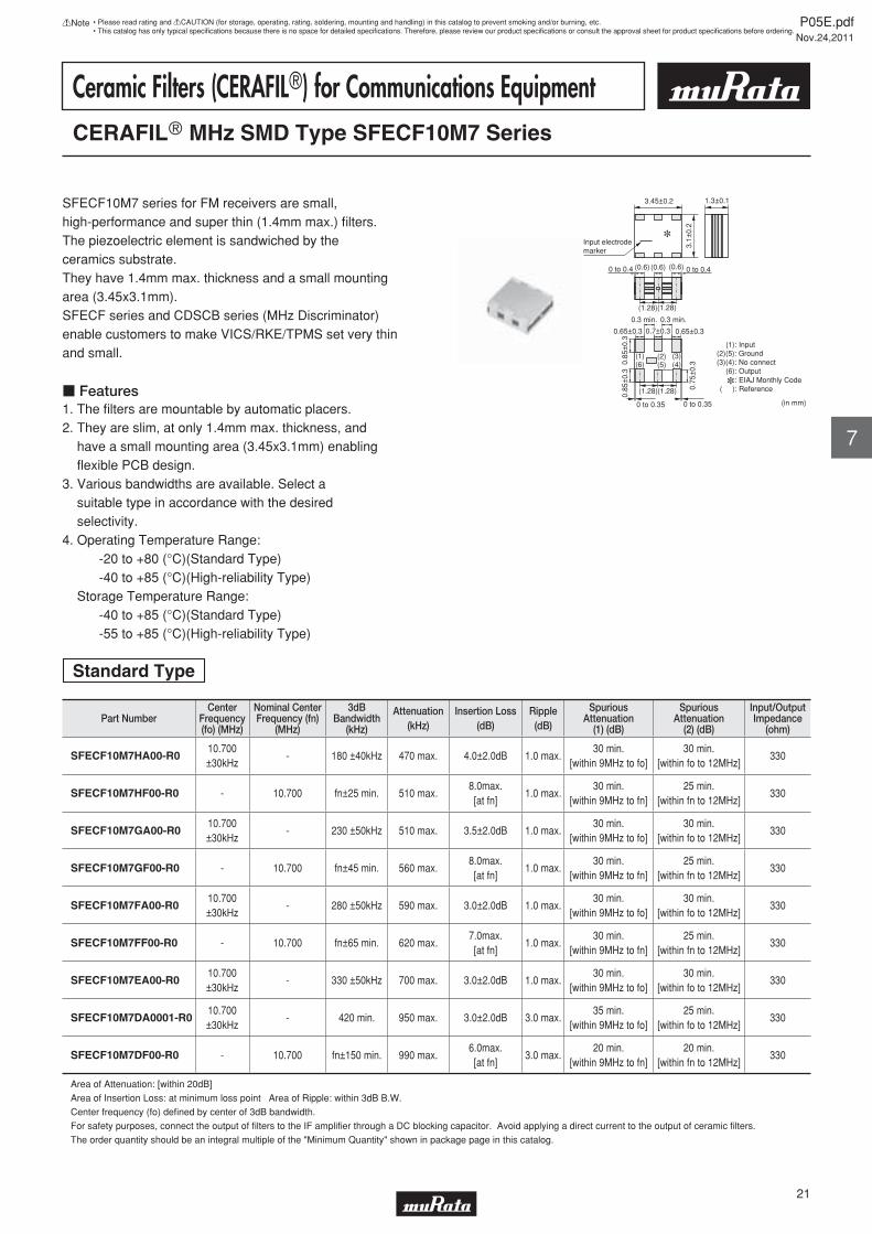
Ceramic Filters (CERAFILr) for Communications EquipmentCERAFILr MHz SMD Type SFECF10M7 Series
SFECF10M7 series for FM receivers are small, high-performance and super thin (1.4mm max.) fi lters. The piezoelectric element is sandwiched by the ceramics substrate.They have 1.4mm max. thickness and a small mounting area (3.45x3.1mm).SFECF series and CDSCB series (MHz Discriminator) enable customers to make VICS/RKE/TPMS set very thin and small.
c Features1. The fi lters are mountable by automatic placers.2. They are slim, at only 1.4mm max. thickness, and have a small mounting area (3.45x3.1mm) enabling fl exible PCB design. 3. Various bandwidths are available. Select a suitable type in accordance with the desired selectivity.4. Operating Temperature Range: -20 to +80 (°C)(Standard Type) -40 to +85 (°C)(High-reliability Type) Storage Temperature Range: -40 to +85 (°C)(Standard Type) -55 to +85 (°C)(High-reliability Type)
0.75
±0.
3
(in mm)
1.3±0.1
3.1±
0.2
3.45±0.2
(0.6) (0.6) (0.6)
(1.28)(1.28)
0 to 0.4
(6)
(1.28)(1.28)
0.65±0.3
0.85
±0.
30.
85±
0.3
0 to 0.35 0 to 0.35
0 to 0.4
(5) (4)(1) (2) (3)
0.65±0.3
0.3 min.0.3 min.
: EIAJ Monthly Code: Reference( )
(1): Input(2)(5): Ground(3)(4): No connect
(6): Output
0.7±0.3
Input electrode marker
Standard Type
Part NumberCenter
Frequency(fo) (MHz)
Nominal CenterFrequency (fn)
(MHz)
3dBBandwidth
(kHz)
Attenuation(kHz)
Insertion Loss(dB)
Ripple(dB)
SpuriousAttenuation
(1) (dB)
SpuriousAttenuation
(2) (dB)
Input/OutputImpedance
(ohm)
SFECF10M7HA00-R010.700±30kHz
- 180 ±40kHz 470 max. 4.0±2.0dB 1.0 max.30 min.
[within 9MHz to fo]30 min.
[within fo to 12MHz]330
SFECF10M7HF00-R0 - 10.700 fn±25 min. 510 max.8.0max. [at fn]
1.0 max.30 min.
[within 9MHz to fn]25 min.
[within fn to 12MHz]330
SFECF10M7GA00-R010.700±30kHz
- 230 ±50kHz 510 max. 3.5±2.0dB 1.0 max.30 min.
[within 9MHz to fo]30 min.
[within fo to 12MHz]330
SFECF10M7GF00-R0 - 10.700 fn±45 min. 560 max.8.0max. [at fn]
1.0 max.30 min.
[within 9MHz to fn]25 min.
[within fn to 12MHz]330
SFECF10M7FA00-R010.700±30kHz
- 280 ±50kHz 590 max. 3.0±2.0dB 1.0 max.30 min.
[within 9MHz to fo]30 min.
[within fo to 12MHz]330
SFECF10M7FF00-R0 - 10.700 fn±65 min. 620 max.7.0max. [at fn]
1.0 max.30 min.
[within 9MHz to fn]25 min.
[within fn to 12MHz]330
SFECF10M7EA00-R010.700±30kHz
- 330 ±50kHz 700 max. 3.0±2.0dB 1.0 max.30 min.
[within 9MHz to fo]30 min.
[within fo to 12MHz]330
SFECF10M7DA0001-R010.700±30kHz
- 420 min. 950 max. 3.0±2.0dB 3.0 max.35 min.
[within 9MHz to fo]25 min.
[within fo to 12MHz]330
SFECF10M7DF00-R0 - 10.700 fn±150 min. 990 max.6.0max. [at fn]
3.0 max.20 min.
[within 9MHz to fn]20 min.
[within fn to 12MHz]330
Area of Attenuation: [within 20dB]
Area of Insertion Loss: at minimum loss point Area of Ripple: within 3dB B.W.
Center frequency (fo) defi ned by center of 3dB bandwidth.
For safety purposes, connect the output of fi lters to the IF amplifi er through a DC blocking capacitor. Avoid applying a direct current to the output of ceramic fi lters.
The order quantity should be an integral multiple of the "Minimum Quantity" shown in package page in this catalog.
P05E.pdfNov.24,2011
21
!Note • Please read rating and !CAUTION (for storage, operating, rating, soldering, mounting and handling) in this catalog to prevent smoking and/or burning, etc.• This catalog has only typical specifi cations because there is no space for detailed specifi cations. Therefore, please review our product specifi cations or consult the approval sheet for product specifi cations before ordering.
7
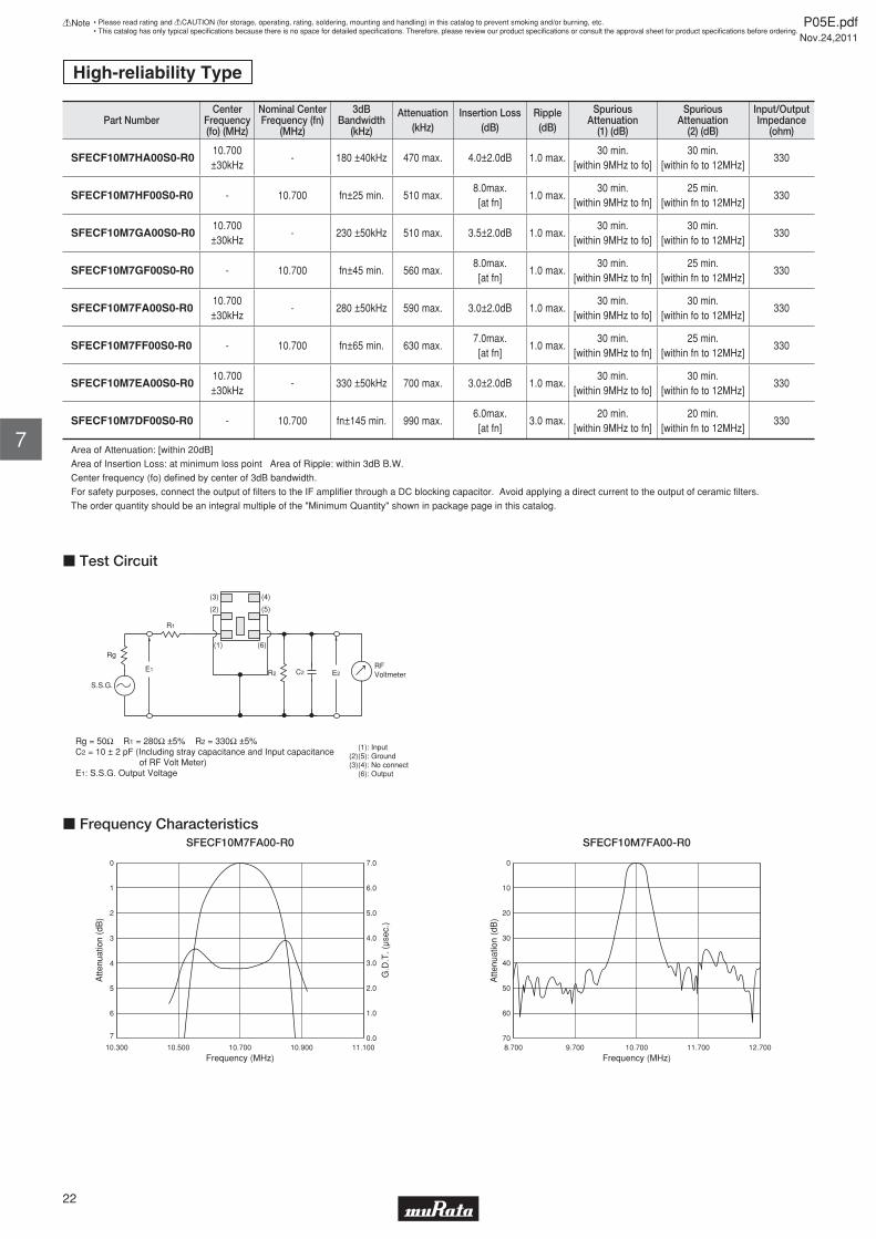
High-reliability Type
Part NumberCenter
Frequency(fo) (MHz)
Nominal CenterFrequency (fn)
(MHz)
3dBBandwidth
(kHz)
Attenuation(kHz)
Insertion Loss(dB)
Ripple(dB)
SpuriousAttenuation
(1) (dB)
SpuriousAttenuation
(2) (dB)
Input/OutputImpedance
(ohm)
SFECF10M7HA00S0-R010.700±30kHz
- 180 ±40kHz 470 max. 4.0±2.0dB 1.0 max.30 min.
[within 9MHz to fo]30 min.
[within fo to 12MHz]330
SFECF10M7HF00S0-R0 - 10.700 fn±25 min. 510 max.8.0max. [at fn]
1.0 max.30 min.
[within 9MHz to fn]25 min.
[within fn to 12MHz]330
SFECF10M7GA00S0-R010.700±30kHz
- 230 ±50kHz 510 max. 3.5±2.0dB 1.0 max.30 min.
[within 9MHz to fo]30 min.
[within fo to 12MHz]330
SFECF10M7GF00S0-R0 - 10.700 fn±45 min. 560 max.8.0max. [at fn]
1.0 max.30 min.
[within 9MHz to fn]25 min.
[within fn to 12MHz]330
SFECF10M7FA00S0-R010.700±30kHz
- 280 ±50kHz 590 max. 3.0±2.0dB 1.0 max.30 min.
[within 9MHz to fo]30 min.
[within fo to 12MHz]330
SFECF10M7FF00S0-R0 - 10.700 fn±65 min. 630 max.7.0max. [at fn]
1.0 max.30 min.
[within 9MHz to fn]25 min.
[within fn to 12MHz]330
SFECF10M7EA00S0-R010.700±30kHz
- 330 ±50kHz 700 max. 3.0±2.0dB 1.0 max.30 min.
[within 9MHz to fo]30 min.
[within fo to 12MHz]330
SFECF10M7DF00S0-R0 - 10.700 fn±145 min. 990 max.6.0max. [at fn]
3.0 max.20 min.
[within 9MHz to fn]20 min.
[within fn to 12MHz]330
Area of Attenuation: [within 20dB]
Area of Insertion Loss: at minimum loss point Area of Ripple: within 3dB B.W.
Center frequency (fo) defi ned by center of 3dB bandwidth.
For safety purposes, connect the output of fi lters to the IF amplifi er through a DC blocking capacitor. Avoid applying a direct current to the output of ceramic fi lters.
The order quantity should be an integral multiple of the "Minimum Quantity" shown in package page in this catalog.
(1)
(2)
(3)
(6)
(5)
(4)
R2 C2 E2RFVoltmeter
R1
E1
S.S.G.
Rg
Rg = 50Ω R1 = 280Ω ±5% R2 = 330Ω ±5%C2 = 10 ± 2 pF (Including stray capacitance and Input capacitance of RF Volt Meter)E1: S.S.G. Output Voltage
: Input: Ground: No connect: Output
(1)(2)(5)(3)(4)
(6)
c Test Circuit
7.0
6.0
5.0
4.0
3.0
2.0
1.0
0.0
Frequency (MHz)
Atte
nuat
ion
(dB
)
10.300 10.500 10.700 10.900 11.100
G.D
.T. (
μsec
.)
7
6
5
4
3
2
1
0
c Frequency CharacteristicsSFECF10M7FA00-R0
Frequency (MHz)
Atte
nuat
ion
(dB
)
8.700 9.700 10.700 11.700 12.700
0
10
20
30
40
50
60
70
SFECF10M7FA00-R0
P05E.pdfNov.24,2011
22
!Note • Please read rating and !CAUTION (for storage, operating, rating, soldering, mounting and handling) in this catalog to prevent smoking and/or burning, etc.• This catalog has only typical specifi cations because there is no space for detailed specifi cations. Therefore, please review our product specifi cations or consult the approval sheet for product specifi cations before ordering.
7
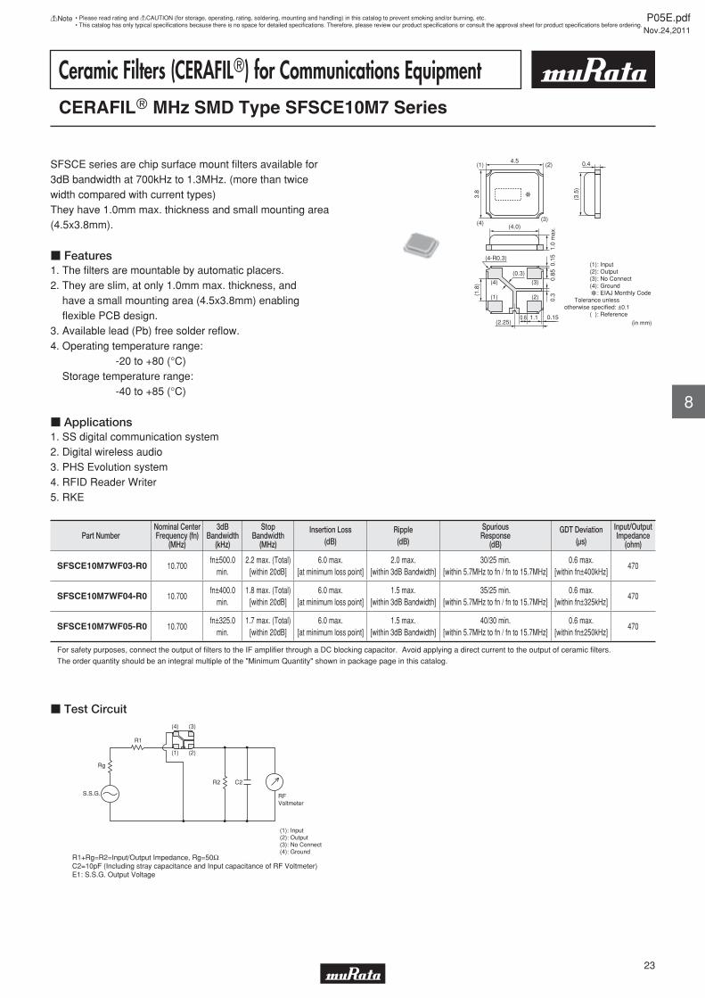
Ceramic Filters (CERAFILr) for Communications EquipmentCERAFILr MHz SMD Type SFSCE10M7 Series
SFSCE series are chip surface mount fi lters available for 3dB bandwidth at 700kHz to 1.3MHz. (more than twice width compared with current types)They have 1.0mm max. thickness and small mounting area (4.5x3.8mm).
c Features1. The fi lters are mountable by automatic placers.2. They are slim, at only 1.0mm max. thickness, and have a small mounting area (4.5x3.8mm) enabling fl exible PCB design.3. Available lead (Pb) free solder refl ow.4. Operating temperature range: -20 to +80 (°C) Storage temperature range: -40 to +85 (°C)
c Applications1. SS digital communication system2. Digital wireless audio3. PHS Evolution system4. RFID Reader Writer5. RKE
(3.5
)
(in mm)
*
0.4
3.8
(1.8
)
4.5(1) (2)
(4)(3)
(4.0)
1.0
max
.0.
850.
150.
3
(1)(2)(3)(4)
Tolerance unlessotherwise specified: ±0.1
( )
: Input: Output: No Connect: Ground: EIAJ Monthly Code
: Reference
*
(2.25)1.10.6 0.15
(4-R0.3)
(0.3)
(1)
(4)
(2)
(3)
Part NumberNominal CenterFrequency (fn)
(MHz)
3dBBandwidth
(kHz)
StopBandwidth
(MHz)
Insertion Loss(dB)
Ripple(dB)
SpuriousResponse
(dB)
GDT Deviation(µs)
Input/OutputImpedance
(ohm)
SFSCE10M7WF03-R0 10.700fn±500.0
min.2.2 max. (Total)
[within 20dB]6.0 max.
[at minimum loss point]2.0 max.
[within 3dB Bandwidth]30/25 min.
[within 5.7MHz to fn / fn to 15.7MHz]0.6 max.
[within fn±400kHz]470
SFSCE10M7WF04-R0 10.700fn±400.0
min.1.8 max. (Total)
[within 20dB]6.0 max.
[at minimum loss point]1.5 max.
[within 3dB Bandwidth]35/25 min.
[within 5.7MHz to fn / fn to 15.7MHz]0.6 max.
[within fn±325kHz]470
SFSCE10M7WF05-R0 10.700fn±325.0
min.1.7 max. (Total)
[within 20dB]6.0 max.
[at minimum loss point]1.5 max.
[within 3dB Bandwidth]40/30 min.
[within 5.7MHz to fn / fn to 15.7MHz]0.6 max.
[within fn±250kHz]470
For safety purposes, connect the output of fi lters to the IF amplifi er through a DC blocking capacitor. Avoid applying a direct current to the output of ceramic fi lters.
The order quantity should be an integral multiple of the "Minimum Quantity" shown in package page in this catalog.
R1+Rg=R2=Input/Output Impedance, Rg=50ΩC2=10pF (Including stray capacitance and Input capacitance of RF Voltmeter)E1: S.S.G. Output Voltage
(1): Input(2): Output(3): No Connect(4): Ground
RFVoltmeter
C2R2
R1
Rg
S.S.G.
(4)
(1)
(3)
(2)
c Test Circuit
P05E.pdfNov.24,2011
23
!Note • Please read rating and !CAUTION (for storage, operating, rating, soldering, mounting and handling) in this catalog to prevent smoking and/or burning, etc.• This catalog has only typical specifi cations because there is no space for detailed specifi cations. Therefore, please review our product specifi cations or consult the approval sheet for product specifi cations before ordering.
8
2.0
1.6
1.2
0.8
0.4
0.0
Frequency (MHz)
Atte
nuat
ion
(dB
)
G.D
.T. (
μsec
.)
11.10010.3009.500 11.90011.50010.7009.900
0
2
4
6
8
10
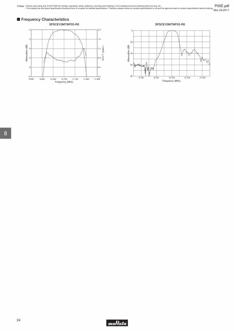
c Frequency CharacteristicsSFSCE10M7WF03-R0
Frequency (MHz)6.700 8.700 10.700 12.700 14.700
Atte
nuat
ion
(dB
)
0
20
40
60
80
SFSCE10M7WF03-R0
P05E.pdfNov.24,2011
24
!Note • Please read rating and !CAUTION (for storage, operating, rating, soldering, mounting and handling) in this catalog to prevent smoking and/or burning, etc.• This catalog has only typical specifi cations because there is no space for detailed specifi cations. Therefore, please review our product specifi cations or consult the approval sheet for product specifi cations before ordering.
8
MHz SMD Type CERAFILr Notice
Continued on the following page.
Filter is soldered twice within the following temperature conditions.
1. Standard Reflow Soldering Conditions(1) Reflow
Filter is soldered at +350±5°C for 3.0±0.5 seconds. The soldering iron should not touch the filter while soldering.
(2) Soldering Iron
The component is recommended with placement machines that employ optical placement capabilities. The component might be damaged by excessive mechanical force. Please make sure that you have evaluated by using placement machines before going into mass production. Do not use placement machines that utilize mechanical positioning. Please contact Murata for details beforehand.
(3) Condition for Placement Machines
(a) The component may be damaged if excess mechanical stress is applied to it mounted on the printed circuit board.
(b) Design layout of components on the PC board to minimize the stress imposed on the warp or flexure of the board.
(c) After installing components, if solder is excessively applied to the circuit board, mechanical stress will cause destruction resistance characteristics to degrade. To prevent this, be extremely careful in determining shape and dimension before designing the circuit board diagram.
(d) When the positioning claws and pick-up nozzle are worn, the load is applied to the components while positioning is concentrated on positioning accuracy, etc. Careful checking and maintenance are necessary to prevent unexpected trouble.
(e) When correcting components with a soldering iron, the tip of the soldering iron should not directly touch the component. Depending on the soldering conditions, the effective area of terminations may be reduced. Solder containing Ag should be used to prevent the electrode erosion.
(f) Do not use strong acidity flux, more than 0.2wt% chlorine content, in reflow soldering.
(4) Other
o Soldering and Mounting
Tem
pera
ture
(°C
)
100
230
260
30 sec.min.
40 sec.max.
Peak(260°C max.)
Pre-heating(150-180°C)
Heating(230°C)
GradualCooling
120 sec.min.
60-120 sec.
[Component Direction]
[Component Layout Close to Board]
Place the component lateral to the direction in which stress acts.
Susceptibility to stress is in the order of : A>C>B
B
A CSlit
Perforation
c SFECF10M7 Series Notice
P05E.pdfNov.24,2011
25
!Note • Please read rating and !CAUTION (for storage, operating, rating, soldering, mounting and handling) in this catalog to prevent smoking and/or burning, etc.• This catalog has only typical specifi cations because there is no space for detailed specifi cations. Therefore, please review our product specifi cations or consult the approval sheet for product specifi cations before ordering.
MHz SMD Type CERAFILr Notice
o Storage and Operating Conditions
o RatingThe component may be damaged if excessive mechanical stress is applied.
o Handling1. Accurate test circuit values are required to measure
electrical characteristics. Miscorrelation may be caused if there is any deviation, especially stray capacitance, from the test circuit in the specification.
2. The components, packed in a moisture proof bag (dry pack), are sensitive to moisture. The following treatment is required before applying reflow soldering, to avoid reliability degradation caused by thermal stress. When unpacked, store the component in an atmosphere of reflow 30°C and below 60%R.H., and solder within 1 week.
3. For safety purposes, connect the output of filters to the IF amplifier through a D.C. blocking capacitor. Avoid applying a direct current to the output of ceramic filters.
1. Product Storage ConditionPlease store the products in a room where the temperature/humidity is stable, and avoid places where there are large temperature changes. Please store the products under the following conditions: Temperature: -10 to +40°CHumidity: 15 to 85% R.H.
2. Expiration Date on StorageExpiration date (shelf life) of the products is six months after delivery under the conditions of a sealed and unopened package. Please use the products within six months after delivery. If you store the products for a long time (more than six months), use carefully because solderability may be degraded due to storage under poor conditions.Please confirm solderability and characteristics for the products regularly.
3. Notice on Product Storage(1) Please do not store the products in a chemical
atmosphere (Acids, Alkali, Bases, Organic gas, Sulfides and so on), because the characteristics may be reduced in quality and may be degraded in solderability due to storage in a chemical atmosphere.
(2) Please do not put the products directly on the floor without anything under them to avoid damp places and/or dusty places.
(3) Please do not store the products in places such as a damp heated place or any place exposed to direct sunlight or excessive vibration.
(4) Please use the products immediately after the package is opened, because the characteristics may be reduced in quality and/or be degraded in solderability due to storage under poor condition.
(5) Please do not drop the products to avoid cracking of ceramic element.
4. OtherPlease be sure to consult with our sales representative or engineer whenever the products are to be used in conditions not listed above.
Continued from the preceding page.
Do not clean or wash the component as it is not hermetically sealed.
2. Wash
In case of overcoating the component, conditions such as material of resin, cure temperature, and so on should be evaluated well.
3. Coating
P05E.pdfNov.24,2011
26
!Note • Please read rating and !CAUTION (for storage, operating, rating, soldering, mounting and handling) in this catalog to prevent smoking and/or burning, etc.• This catalog has only typical specifi cations because there is no space for detailed specifi cations. Therefore, please review our product specifi cations or consult the approval sheet for product specifi cations before ordering.
MHz SMD Type CERAFILr Notice
Continued on the following page.
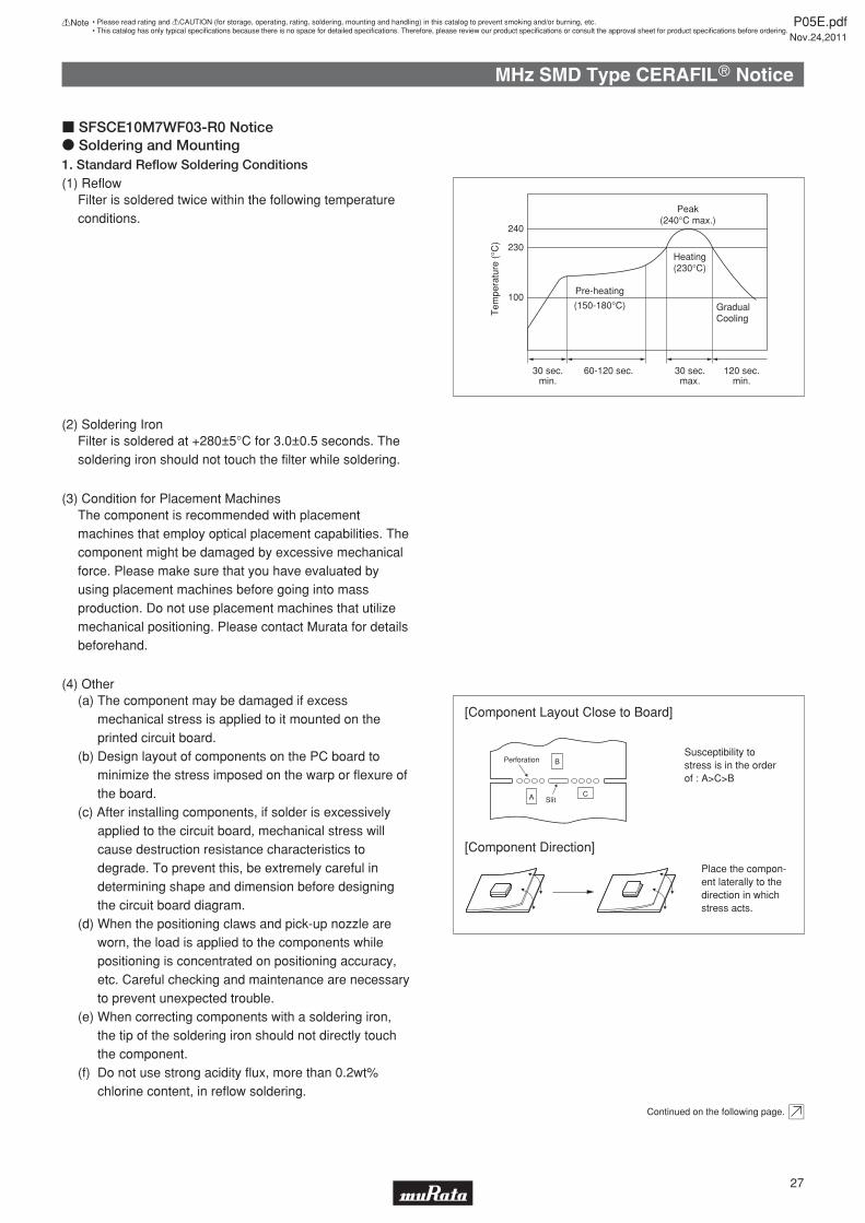
Filter is soldered twice within the following temperature conditions.
1. Standard Reflow Soldering Conditions(1) Reflow
Filter is soldered at +280±5°C for 3.0±0.5 seconds. The soldering iron should not touch the filter while soldering.
(2) Soldering Iron
The component is recommended with placement machines that employ optical placement capabilities. The component might be damaged by excessive mechanical force. Please make sure that you have evaluated by using placement machines before going into mass production. Do not use placement machines that utilize mechanical positioning. Please contact Murata for details beforehand.
(3) Condition for Placement Machines
(a) The component may be damaged if excess mechanical stress is applied to it mounted on the printed circuit board.
(b) Design layout of components on the PC board to minimize the stress imposed on the warp or flexure of the board.
(c) After installing components, if solder is excessively applied to the circuit board, mechanical stress will cause destruction resistance characteristics to degrade. To prevent this, be extremely careful in determining shape and dimension before designing the circuit board diagram.
(d) When the positioning claws and pick-up nozzle are worn, the load is applied to the components while positioning is concentrated on positioning accuracy, etc. Careful checking and maintenance are necessary to prevent unexpected trouble.
(e) When correcting components with a soldering iron, the tip of the soldering iron should not directly touch the component.
(f) Do not use strong acidity flux, more than 0.2wt% chlorine content, in reflow soldering.
(4) Other
o Soldering and Mounting
Peak(240°C max.)
Heating(230°C)
GradualCooling
Pre-heating
(150-180°C)100
230
240
Tem
pera
ture
(°C
)
60-120 sec. 30 sec.max.
30 sec.min.
120 sec.min.
[Component Direction]
Place the compon-ent laterally to the direction in which stress acts.
[Component Layout Close to Board]
Susceptibility to stress is in the order of : A>C>B
B
A CSlit
Perforation
c SFSCE10M7WF03-R0 Notice
P05E.pdfNov.24,2011
27
!Note • Please read rating and !CAUTION (for storage, operating, rating, soldering, mounting and handling) in this catalog to prevent smoking and/or burning, etc.• This catalog has only typical specifi cations because there is no space for detailed specifi cations. Therefore, please review our product specifi cations or consult the approval sheet for product specifi cations before ordering.

MHz SMD Type CERAFILr Notice
o Handling1. Accurate test circuit values are required to measure
electrical characteristics. Miscorrelation may be caused if there is any deviation, especially stray capacitance, from the test circuit in the specification.
2. For safety purposes, connect the output of filters to the IF amplifier through a D.C. blocking capacitor. Avoid applying a direct current to the output of ceramic filters.
Continued from the preceding page.
Do not clean or wash the component as it is not hermetically sealed.
2. Wash
In case of overcoating the component, conditions such as material of resin, cure temperature, and so on should be evaluated well.
3. Coating
o Storage and Operating Conditions1. Product Storage Condition
Please store the products in a room where the temperature/humidity is stable, and avoid places where there are large temperature changes. Please store the products under the following conditions: Temperature: -10 to + 40°CHumidity: 15 to 85% R.H.
2. Expiration Date on StorageExpiration date (shelf life) of the products is six months after delivery under the conditions of a sealed and unopened package. Please use the products within six months after delivery. If you store the products for a long time (more than six months), use carefully because solderability may be degraded due to storage under poor conditions. Please confirm solderability and characteristics for the products regularly.
3. Notice on Product Storage(1) Please do not store the products in a chemical
atmosphere (Acids, Alkali, Bases, Organic gas, Sulfides and so on), because the characteristics may be reduced in quality and may be degraded in solderability due to storage in a chemical atmosphere.
(2) Please do not put the products directly on the floor without anything under them to avoid damp places and/or dusty places.
(3) Please do not store the products in places such as a damp heated place or any place exposed to direct sunlight or excessive vibration.
(4) Please use the products immediately after the package is opened, because the characteristics may be reduced in quality and/or be degraded in solderability due to storage under poor condition.
(5) Please do not drop the products to avoid cracking of ceramic element.
4. OtherPlease be sure to consult with our sales representative or engineer whenever the products are to be used in conditions not listed above.
o RatingThe component may be damaged if excessive mechanical stress is applied.
P05E.pdfNov.24,2011
28
!Note • Please read rating and !CAUTION (for storage, operating, rating, soldering, mounting and handling) in this catalog to prevent smoking and/or burning, etc.• This catalog has only typical specifi cations because there is no space for detailed specifi cations. Therefore, please review our product specifi cations or consult the approval sheet for product specifi cations before ordering.

MHz SMD Type CERAFILr Notice
Continued on the following page.
Filter is soldered twice within the following temperature conditions.
1. Standard Reflow Soldering Conditions(1) Reflow
Filter is soldered at +280±5°C for 3.0±0.5 seconds. The soldering iron should not touch the filter while soldering.
(2) Soldering Iron
The component is recommended with placement machines that employ optical placement capabilities. The component might be damaged by excessive mechanical force. Please make sure that you have evaluated by using placement machines before going into mass production. Do not use placement machines that utilize mechanical positioning. Please contact Murata for details beforehand.
(3) Condition for Placement Machines
(a) The component may be damaged if excess mechanical stress is applied to it mounted on the printed circuit board.
(b) Design layout of components on the PC board to minimize the stress imposed on the warp or flexure of the board.
(c) After installing components, if solder is excessively applied to the circuit board, mechanical stress will cause destruction resistance characteristics to degrade. To prevent this, be extremely careful in determining shape and dimension before designing the circuit board diagram.
(d) When the positioning claws and pick-up nozzle are worn, the load is applied to the components while positioning is concentrated on positioning accuracy, etc. Careful checking and maintenance are necessary to prevent unexpected trouble.
(e) When correcting components with a soldering iron, the tip of the soldering iron should not directly touch the component.
(f) Do not use strong acidity flux, more than 0.2wt% chlorine content, in reflow soldering.
(4) Other
o Soldering and Mounting
[Component Direction]
Place the compon-ent laterally to the direction in which stress acts.
[Component Layout Close to Board]
Susceptibility to stress is in the order of : A>C>B
B
A CSlit
Perforation
Peak(260°C max.)
Heating(230°C)
GradualCooling
Pre-heating
(150-180°C)100
230
260
Tem
pera
ture
(°C
)
60-120 sec. 40 sec.max.
30 sec.min.
120 sec.min.
c SFSCE10M7WF04/05-R0 Notice
P05E.pdfNov.24,2011
29
!Note • Please read rating and !CAUTION (for storage, operating, rating, soldering, mounting and handling) in this catalog to prevent smoking and/or burning, etc.• This catalog has only typical specifi cations because there is no space for detailed specifi cations. Therefore, please review our product specifi cations or consult the approval sheet for product specifi cations before ordering.
MHz SMD Type CERAFILr Notice
o Handling1. Accurate test circuit values are required to measure
electrical characteristics. Miscorrelation may be caused if there is any deviation, especially stray capacitance, from the test circuit in the specification.
2. For safety purposes, connect the output of filters to the IF amplifier through a D.C. blocking capacitor. Avoid applying a direct current to the output of ceramic filters.
Continued from the preceding page.
Do not clean or wash the component as it is not hermetically sealed.
2. Wash
In case of overcoating the component, conditions such as material of resin, cure temperature, and so on should be evaluated well.
3. Coating
o Storage and Operating Conditions1. Product Storage Condition
Please store the products in a room where the temperature/humidity is stable, and avoid places where there are large temperature changes. Please store the products under the following conditions: Temperature: -10 to + 40°CHumidity: 15 to 85% R.H.
2. Expiration Date on StorageExpiration date (shelf life) of the products is six months after delivery under the conditions of a sealed and unopened package. Please use the products within six months after delivery. If you store the products for a long time (more than six months), use carefully because solderability may be degraded due to storage under poor conditions. Please confirm solderability and characteristics for the products regularly.
3. Notice on Product Storage(1) Please do not store the products in a chemical
atmosphere (Acids, Alkali, Bases, Organic gas, Sulfides and so on), because the characteristics may be reduced in quality and may be degraded in solderability due to storage in a chemical atmosphere.
(2) Please do not put the products directly on the floor without anything under them to avoid damp places and/or dusty places.
(3) Please do not store the products in places such as a damp heated place or any place exposed to direct sunlight or excessive vibration.
(4) Please use the products immediately after the package is opened, because the characteristics may be reduced in quality and/or be degraded in solderability due to storage under poor condition.
(5) Please do not drop the products to avoid cracking of ceramic element.
4. OtherPlease be sure to consult with our sales representative or engineer whenever the products are to be used in conditions not listed above.
o RatingThe component may be damaged if excessive mechanical stress is applied.
P05E.pdfNov.24,2011
30
!Note • Please read rating and !CAUTION (for storage, operating, rating, soldering, mounting and handling) in this catalog to prevent smoking and/or burning, etc.• This catalog has only typical specifi cations because there is no space for detailed specifi cations. Therefore, please review our product specifi cations or consult the approval sheet for product specifi cations before ordering.
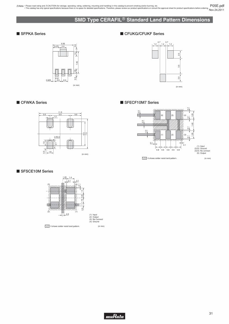
SMD Type CERAFILr Standard Land Pattern Dimensions
(in mm)
2.02.4756.95
1.6
1.55
7.45
0.8
0.9
0.925 2.0 2.0
1.1
c SFPKA Series
(in mm)
1.20.7 0.7
1.4 1.2
2.0
3.5
2.0
c CFUKG/CFUKF Series
(in mm)
1.23.03.0 5.5
4-R3.0
11.5
7.5
6.5
1.6
2.1
1.80.5
c CFWKA Series
InputGroundNo connectOutput
(1): (2)(5): (3)(4):
(6):
(in mm)It shows solder resist land pattern.
1.05
1.40
1.05
0.1
0.1
0.1
0.1
0.8 0.6 0.8 0.6 0.8
0.10.1
0.3
0.3
0.3
(6) (5) (4)
(1) (2) (3)
c SFECF10M7 Series
(in mm)It shows solder resist land pattern.
(1): Input(2): Output(3): No Connect(4): Ground
0.5
0.5
1.4
0.1 0.1
0.1
1.05
(3) (4)
(2) (1)
0.8
1.15
1.3
c SFSCE10M Series
P05E.pdfNov.24,2011
31
!Note • Please read rating and !CAUTION (for storage, operating, rating, soldering, mounting and handling) in this catalog to prevent smoking and/or burning, etc.• This catalog has only typical specifi cations because there is no space for detailed specifi cations. Therefore, please review our product specifi cations or consult the approval sheet for product specifi cations before ordering.
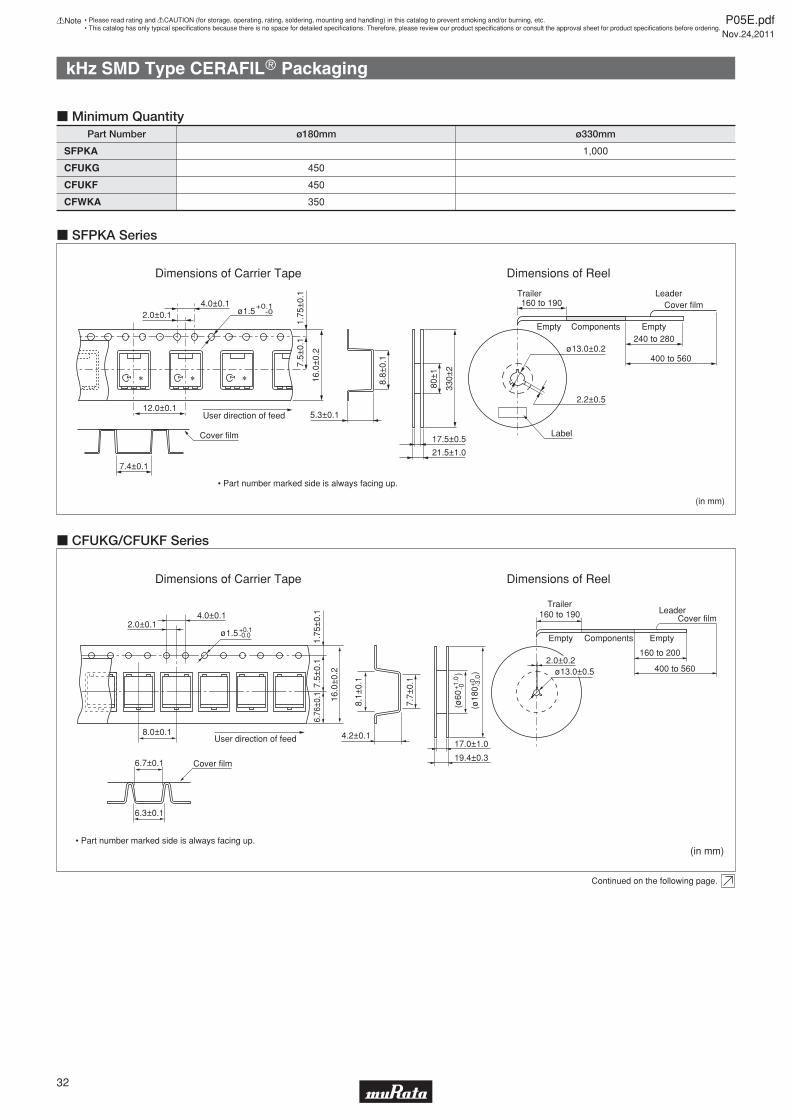
kHz SMD Type CERAFILr Packaging
Part Number ø180mm
450
450
350
ø330mm
1,000SFPKA
CFUKG
CFUKF
CFWKA
c Minimum Quantity
Dimensions of Carrier Tape
User direction of feed12.0±0.1
16.0
±0.
2
8.8±
0.1
7.5±
0.1
1.75
±0.
14.0±0.1
2.0±0.1
5.3±0.1
ø1.5
7.4±0.1
+0.1-0
Cover film
(in mm)
Dimensions of Reel
Label
ø13.0±0.2
2.2±0.5
21.5±1.033
0±2
80±
1
240 to 280
400 to 560
160 to 190
17.5±0.5
EmptyComponents
Cover film
Empty
Trailer Leader
c SFPKA Series
+1.
0-0 +
0-3
.0
Dimensions of Carrier Tape Dimensions of Reel
(in mm)
LeaderCover film
Empty EmptyComponents
Trailer160 to 190
160 to 200
400 to 560
(ø60
)
(ø18
0
)
17.0±1.0
19.4±0.3
ø13.0±0.52.0±0.2
Cover film
+0.1-0.0
4.0±0.1
7.5±
0.1
1.75
±0.
16.
76±0
.1 16.0
±0.
2
8.1±
0.1
4.2±0.1
7.7±
0.1
8.0±0.1
6.7±0.1
6.3±0.1
2.0±0.1ø1.5
c CFUKG/CFUKF Series
Continued on the following page.
P05E.pdfNov.24,2011
32
!Note • Please read rating and !CAUTION (for storage, operating, rating, soldering, mounting and handling) in this catalog to prevent smoking and/or burning, etc.• This catalog has only typical specifi cations because there is no space for detailed specifi cations. Therefore, please review our product specifi cations or consult the approval sheet for product specifi cations before ordering.
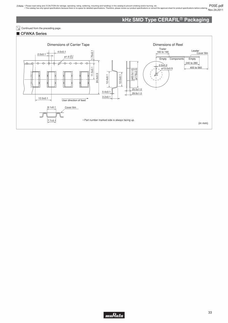
kHz SMD Type CERAFILr Packaging
Continued from the preceding page.
Dimensions of Carrier Tape Dimensions of Reel
(in mm)
User direction of feed
+0.1-0.0
4.0±0.1
11.5
±0.
11.
75±
0.1
24.0
±0.
3
12.4
±0.
1
3.2±0.1
0.4±0.1
12.0
±0.
1
12.0±0.1
2.0±0.1ø1.5
Cover film8.1±0.1
7.7±0.1
(ø62
.0±1
.0)
(ø17
8±2.
0)
25.5±1.0
29.9±1.0
LeaderCover film
Empty EmptyComponents
Trailer160 to 190
240 to 280
400 to 560ø13.0±0.52.0±0.2
c CFWKA Series
P05E.pdfNov.24,2011
33
!Note • Please read rating and !CAUTION (for storage, operating, rating, soldering, mounting and handling) in this catalog to prevent smoking and/or burning, etc.• This catalog has only typical specifi cations because there is no space for detailed specifi cations. Therefore, please review our product specifi cations or consult the approval sheet for product specifi cations before ordering.
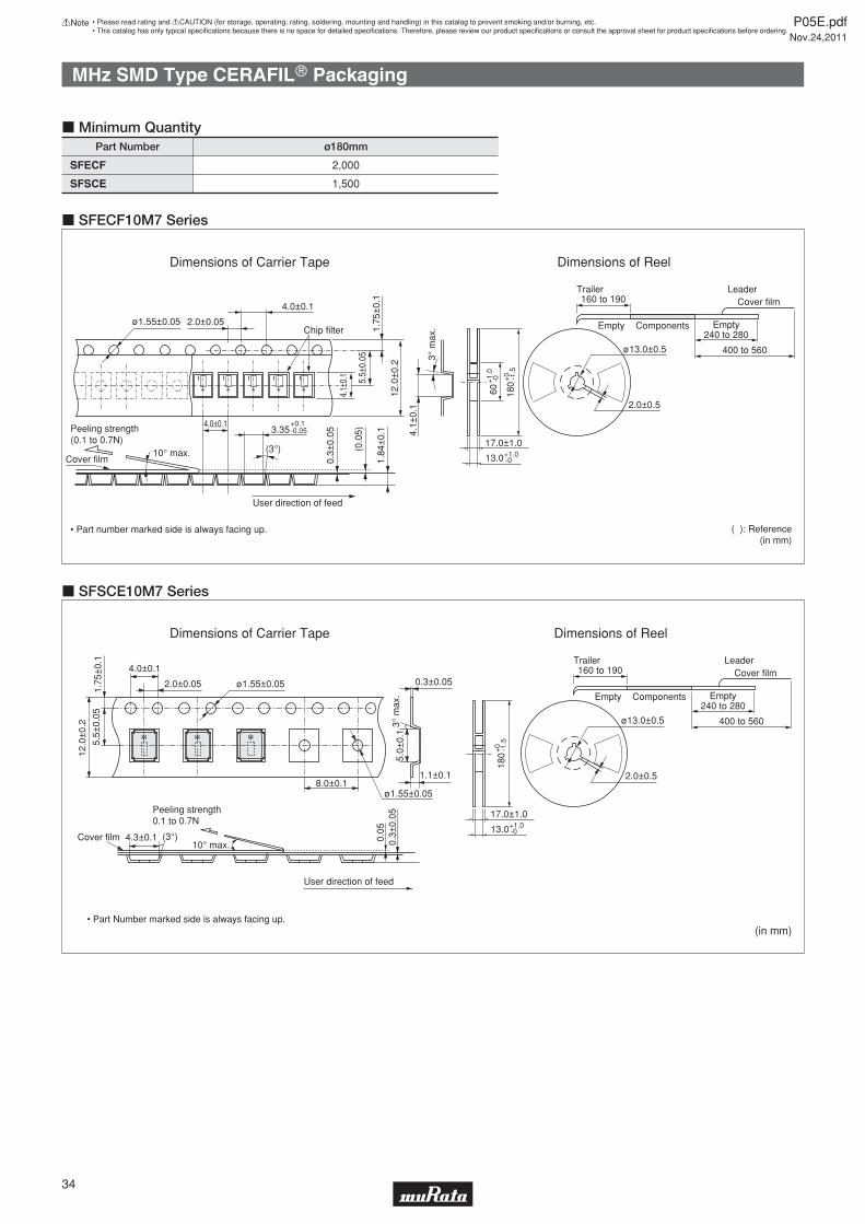
MHz SMD Type CERAFILr Packaging
Part Number ø180mm
2,000
1,500
SFECF
SFSCE
c Minimum Quantity
( ): Reference(in mm)
Dimensions of Carrier Tape Dimensions of Reel
ø13.0±0.5
2.0±0.5
240 to 280
400 to 560
160 to 190
EmptyComponents
Cover film
Empty
Trailer Leader
17.0±1.0+1.0-013.0
+0 -1.5
180+
1.0
-060
Chip filterø1.55±0.05
User direction of feed
Cover film
Peeling strength (0.1 to 0.7N)
0.3±
0.05
1.84
±0.
1
(0.0
5)
(3°)10° max.
5.5±
0.05
4.1±
0.1
1.75
±0.
1
3° m
ax.
4.1±
0.1
4.0±0.1
2.0±0.05
4.0±0.13.35
12.0
±0.
2
+0.1-0.05
c SFECF10M7 Series
(in mm)
Dimensions of Carrier Tape Dimensions of Reel
±
±
±±
±
±
(3°)
±
±
±
±
±
±Cover film
±
±
±
Cover filmTrailer
±
c SFSCE10M7 Series
P05E.pdfNov.24,2011
34
!Note • Please read rating and !CAUTION (for storage, operating, rating, soldering, mounting and handling) in this catalog to prevent smoking and/or burning, etc.• This catalog has only typical specifi cations because there is no space for detailed specifi cations. Therefore, please review our product specifi cations or consult the approval sheet for product specifi cations before ordering.
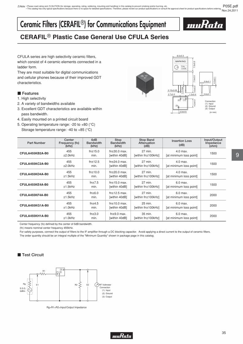
Ceramic Filters (CERAFILr) for Communications EquipmentCERAFILr Plastic Case General Use CFULA Series
CFULA series are high selectivity ceramic fi lters,which consist of 4 ceramic elements connected in a ladder form.They are most suitable for digital communications and cellular phones because of their improved GDT characteristics.
c Features1. High selectivity2. A variety of bandwidths available3. Excellent GDT characteristics are available within pass bandwidth.4. Easily mounted on a printed circuit board5. Operating temperature range: -20 to +80 (°C) Storage temperature range: -40 to +85 (°C)
3.0±
0.3
7.0±
0.3
4.2±
0.3
7.3±
0.3
0.8±0.1
0.6±0.11.2±0.5
8.0±0.3
MARKING
EIAJCODE
3.3±0.5
2.7±0.3
(1)(2)
(3)
0.3±
0.1
1.5
max
.
0.15±0.05
Connection(1): Input(2): Ground(3): Output
(in mm)
Part NumberCenter
Frequency (fo)(kHz)
6dBBandwidth
(kHz)
StopBandwidth
(kHz)
Stop BandAttenuation
(dB)
Insertion Loss(dB)
Input/OutputImpedance
(ohm)
CFULA455KB2A-B0455
±2.0kHzfn±15.0
min.fn±30.0 max.[within 40dB]
27 min.[within fn±100kHz]
4.0 max.[at minimum loss point]
1500
CFULA455KC2A-B0455
±2.0kHzfn±12.5
min.fn±24.0 max.[within 40dB]
27 min.[within fn±100kHz]
4.0 max.[at minimum loss point]
1500
CFULA455KD4A-B0455
±1.5kHzfn±10.0
min.fn±20.0 max.[within 40dB]
27 min.[within fn±100kHz]
4.0 max.[at minimum loss point]
1500
CFULA455KE4A-B0455
±1.5kHzfn±7.5min.
fn±15.0 max.[within 40dB]
27 min.[within fn±100kHz]
6.0 max.[at minimum loss point]
1500
CFULA455KF4A-B0455
±1.5kHzfn±6.0min.
fn±12.5 max.[within 40dB]
27 min.[within fn±100kHz]
6.0 max.[at minimum loss point]
2000
CFULA455KG1A-B0455
±1.0kHzfn±4.5min.
fn±10.0 max.[within 40dB]
25 min.[within fn±100kHz]
6.0 max.[at minimum loss point]
2000
CFULA455KH1A-B0455
±1.0kHzfn±3.0min.
fn±9.0 max.[within 40dB]
35 min.[within fn±100kHz]
6.0 max.[at minimum loss point]
2000
Center frequency (fo) defi ned by the center of 6dB bandwidth.
(fn) means nominal center frequency 455kHz.
For safety purposes, connect the output of fi lters to the IF amplifi er through a DC blocking capacitor. Avoid applying a direct current to the output of ceramic fi lters.
The order quantity should be an integral multiple of the "Minimum Quantity" shown in package page in this catalog.
E1
R1
Rg
S.S.G.0dBm
R2 E2 RF Voltmeter Connection
(1): Input
(2): Ground
(3): Output
(1) (2)(3)
Rg+R1=R2=Input/Output Impedance
c Test Circuit
P05E.pdfNov.24,2011
35
!Note • Please read rating and !CAUTION (for storage, operating, rating, soldering, mounting and handling) in this catalog to prevent smoking and/or burning, etc.• This catalog has only typical specifi cations because there is no space for detailed specifi cations. Therefore, please review our product specifi cations or consult the approval sheet for product specifi cations before ordering.
9
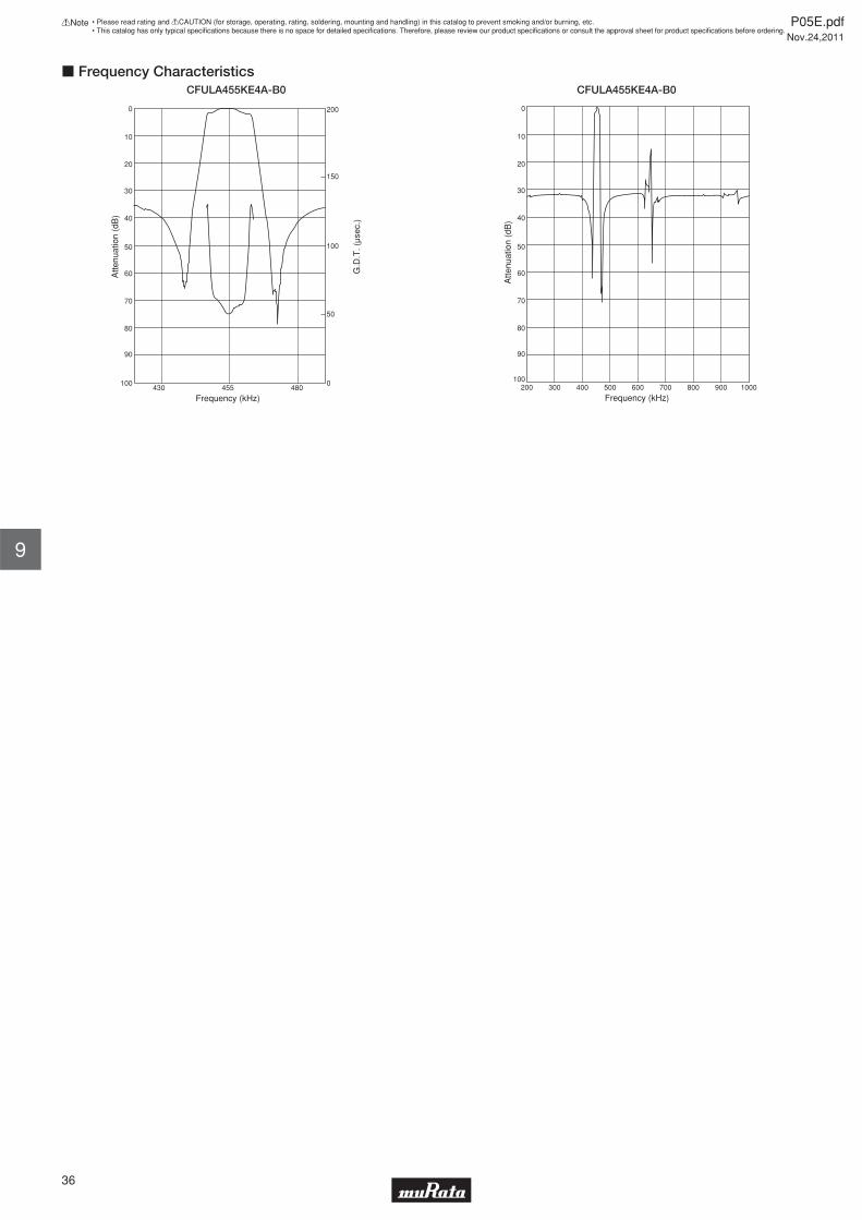
100
40
30
20
10
0A
ttenu
atio
n (d
B)
0
50
100
150
200
G.D
.T. (
μsec
.)
430 455 480
Frequency (kHz)
90
80
70
60
50
c Frequency CharacteristicsCFULA455KE4A-B0
100
40
30
20
10
0
Atte
nuat
ion
(dB
)
200
Frequency (kHz)
90
80
70
60
50
300 400 500 600 700 800 900 1000
CFULA455KE4A-B0
P05E.pdfNov.24,2011
36
!Note • Please read rating and !CAUTION (for storage, operating, rating, soldering, mounting and handling) in this catalog to prevent smoking and/or burning, etc.• This catalog has only typical specifi cations because there is no space for detailed specifi cations. Therefore, please review our product specifi cations or consult the approval sheet for product specifi cations before ordering.
9
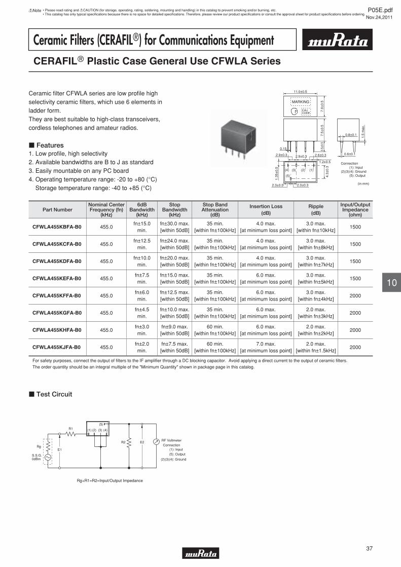
Ceramic Filters (CERAFILr) for Communications EquipmentCERAFILr Plastic Case General Use CFWLA Series
Ceramic fi lter CFWLA series are low profi le high selectivity ceramic fi lters, which use 6 elements in ladder form.They are best suitable to high-class transceivers, cordless telephones and amateur radios.
c Features1. Low profi le, high selectivity2. Available bandwidths are B to J as standard3. Easily mountable on any PC board4. Operating temperature range: -20 to +80 (°C) Storage temperature range: -40 to +85 (°C)
4.3±
0.3
0.15
1.5
max
.
2.3±0.5 2.0±0.3
2.9±0.3
11.0±0.5
MARKING
EIAJCODE
1.2±0.5
(1)(2)(4) (3)
(5)
1.35
±0.
5
7.0±
0.5
3.5±
0.5
0.6±0.1
0.8±0.17.5±
0.5
2.6±0.3
Connection (1): Input(2)(3)(4): Ground (5): Output
(in mm)
2.9—0.32.9±0.3
Part NumberNominal CenterFrequency (fn)
(kHz)
6dBBandwidth
(kHz)
StopBandwidth
(kHz)
Stop BandAttenuation
(dB)
Insertion Loss(dB)
Ripple(dB)
Input/OutputImpedance
(ohm)
CFWLA455KBFA-B0 455.0fn±15.0
min.fn±30.0 max.[within 50dB]
35 min.[within fn±100kHz]
4.0 max.[at minimum loss point]
3.0 max.[within fn±10kHz]
1500
CFWLA455KCFA-B0 455.0fn±12.5
min.fn±24.0 max.[within 50dB]
35 min.[within fn±100kHz]
4.0 max.[at minimum loss point]
3.0 max.[within fn±8kHz]
1500
CFWLA455KDFA-B0 455.0fn±10.0
min.fn±20.0 max.[within 50dB]
35 min.[within fn±100kHz]
4.0 max.[at minimum loss point]
3.0 max.[within fn±7kHz]
1500
CFWLA455KEFA-B0 455.0fn±7.5min.
fn±15.0 max.[within 50dB]
35 min.[within fn±100kHz]
6.0 max.[at minimum loss point]
3.0 max.[within fn±5kHz]
1500
CFWLA455KFFA-B0 455.0fn±6.0min.
fn±12.5 max.[within 50dB]
35 min.[within fn±100kHz]
6.0 max.[at minimum loss point]
3.0 max.[within fn±4kHz]
2000
CFWLA455KGFA-B0 455.0fn±4.5min.
fn±10.0 max.[within 50dB]
35 min.[within fn±100kHz]
6.0 max.[at minimum loss point]
2.0 max.[within fn±3kHz]
2000
CFWLA455KHFA-B0 455.0fn±3.0min.
fn±9.0 max.[within 50dB]
60 min.[within fn±100kHz]
6.0 max.[at minimum loss point]
2.0 max.[within fn±2kHz]
2000
CFWLA455KJFA-B0 455.0fn±2.0min.
fn±7.5 max.[within 50dB]
60 min.[within fn±100kHz]
7.0 max.[at minimum loss point]
2.0 max.[within fn±1.5kHz]
2000
For safety purposes, connect the output of fi lters to the IF amplifi er through a DC blocking capacitor. Avoid applying a direct current to the output of ceramic fi lters.
The order quantity should be an integral multiple of the "Minimum Quantity" shown in package page in this catalog.
E1
R1
R2 E2 RF Voltmeter Connection (1): Input
(5): Output
(2)(3)(4): Ground
Rg
S.S.G.0dBm
(1) (2) (3) (4)
(5)
Rg+R1=R2=Input/Output Impedance
c Test Circuit
P05E.pdfNov.24,2011
37
!Note • Please read rating and !CAUTION (for storage, operating, rating, soldering, mounting and handling) in this catalog to prevent smoking and/or burning, etc.• This catalog has only typical specifi cations because there is no space for detailed specifi cations. Therefore, please review our product specifi cations or consult the approval sheet for product specifi cations before ordering.
10
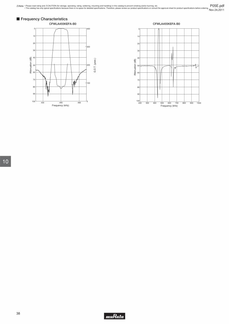
100
40
30
20
10
0A
ttenu
atio
n (d
B)
0
100
200
300
400
G.D
.T. (
μsec
.)
430 455 480
Frequency (kHz)
90
80
70
60
50
c Frequency CharacteristicsCFWLA455KEFA-B0
100
40
30
20
10
0
Atte
nuat
ion
(dB
)
200
Frequency (kHz)
90
80
70
60
50
300 400 500 600 700 800 900 1000
CFWLA455KEFA-B0
P05E.pdfNov.24,2011
38
!Note • Please read rating and !CAUTION (for storage, operating, rating, soldering, mounting and handling) in this catalog to prevent smoking and/or burning, etc.• This catalog has only typical specifi cations because there is no space for detailed specifi cations. Therefore, please review our product specifi cations or consult the approval sheet for product specifi cations before ordering.
10
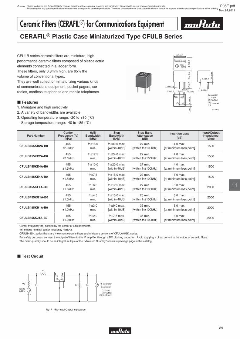
Ceramic Filters (CERAFILr) for Communications EquipmentCERAFILr Plastic Case Miniaturized Type CFULB Series
CFULB series ceramic fi lters are miniature, high-performance ceramic fi lters composed of piezoelectric elements connected in a ladder form.These fi lters, only 6.3mm high, are 65% the volume of conventional types.They are well suited for miniaturizing various kinds of communications equipment, pocket pagers, car radios, cordless telephones and mobile telephones.
c Features1. Miniature and high selectivity2. A variety of bandwidths are available3. Operating temperature range: -20 to +80 (°C) Storage temperature range: -40 to +85 (°C)
4.3±
0.3
1.0
max
.
1.8±0.32.4±0.3
6.5±0.3
0.8±0.3
1.0±
0.3
6.3±
0.3
6.5±
0.3
0.5±0.1
0.7±0.1
3.5±
0.3
0.7±0.3
(1) (2)
(3) (4)
0.15±0.05
Connection(1): Input(2): Output(3)
: Ground(4)
(in mm)
}
MARKING
EIAJCODE
Part NumberCenter
Frequency (fo)(kHz)
6dBBandwidth
(kHz)
StopBandwidth
(kHz)
Stop BandAttenuation
(dB)
Insertion Loss(dB)
Input/OutputImpedance
(ohm)
CFULB455KB2A-B0455
±2.0kHzfn±15.0
min.fn±30.0 max.[within 40dB]
27 min.[within fn±100kHz]
4.0 max.[at minimum loss point]
1500
CFULB455KC2A-B0455
±2.0kHzfn±12.5
min.fn±24.0 max.[within 40dB]
27 min.[within fn±100kHz]
4.0 max.[at minimum loss point]
1500
CFULB455KD4A-B0455
±1.5kHzfn±10.0
min.fn±20.0 max.[within 40dB]
27 min.[within fn±100kHz]
4.0 max.[at minimum loss point]
1500
CFULB455KE4A-B0455
±1.5kHzfn±7.5min.
fn±15.0 max.[within 40dB]
27 min.[within fn±100kHz]
6.0 max.[at minimum loss point]
1500
CFULB455KF4A-B0455
±1.5kHzfn±6.0min.
fn±12.5 max.[within 40dB]
27 min.[within fn±100kHz]
6.0 max.[at minimum loss point]
2000
CFULB455KG1A-B0455
±1.0kHzfn±4.5min.
fn±10.0 max.[within 40dB]
25 min.[within fn±100kHz]
6.0 max.[at minimum loss point]
2000
CFULB455KH1A-B0455
±1.0kHzfn±3.0min.
fn±9.0 max.[within 40dB]
35 min.[within fn±100kHz]
6.0 max.[at minimum loss point]
2000
CFULB455KJ1A-B0455
±1.0kHzfn±2.0min.
fn±7.5 max.[within 40dB]
35 min.[within fn±100kHz]
6.0 max.[at minimum loss point]
2000
Center frequency (fo) defi ned by the center of 6dB bandwidth.
(fn) means nominal center frequency 455kHz.
CFULB455K_series fi lters are 4-element ceramic fi lters and miniature versions of CFULA455K_series.
For safety purposes, connect the output of fi lters to the IF amplifi er through a DC blocking capacitor. Avoid applying a direct current to the output of ceramic fi lters.
The order quantity should be an integral multiple of the "Minimum Quantity" shown in package page in this catalog.
E1
R1
Rg
S.S.G.0dBm
R2 E2RF Voltmeter
Connection
(1)(2)
(3)(4)
: Input: Output: Ground
(1) (2)(3) (4)
Rg+R1=R2=Input/Output Impedance
c Test Circuit
P05E.pdfNov.24,2011
39
!Note • Please read rating and !CAUTION (for storage, operating, rating, soldering, mounting and handling) in this catalog to prevent smoking and/or burning, etc.• This catalog has only typical specifi cations because there is no space for detailed specifi cations. Therefore, please review our product specifi cations or consult the approval sheet for product specifi cations before ordering.
11
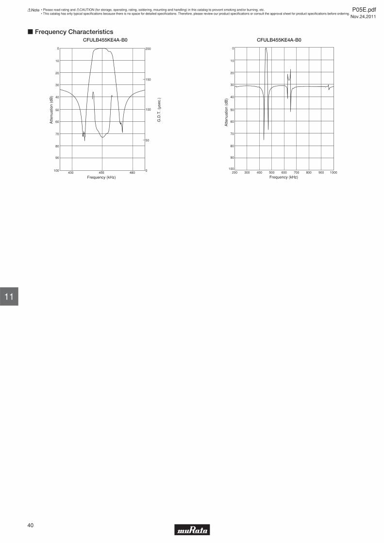
100
40
30
20
10
0A
ttenu
atio
n (d
B)
0
50
100
150
200
G.D
.T. (
μsec
.)
430 455 480
Frequency (kHz)
90
80
70
60
50
c Frequency CharacteristicsCFULB455KE4A-B0
100
40
30
20
10
0
Atte
nuat
ion
(dB
)
200
Frequency (kHz)
90
80
70
60
50
300 400 500 600 700 800 900 1000
CFULB455KE4A-B0
P05E.pdfNov.24,2011
40
!Note • Please read rating and !CAUTION (for storage, operating, rating, soldering, mounting and handling) in this catalog to prevent smoking and/or burning, etc.• This catalog has only typical specifi cations because there is no space for detailed specifi cations. Therefore, please review our product specifi cations or consult the approval sheet for product specifi cations before ordering.
11
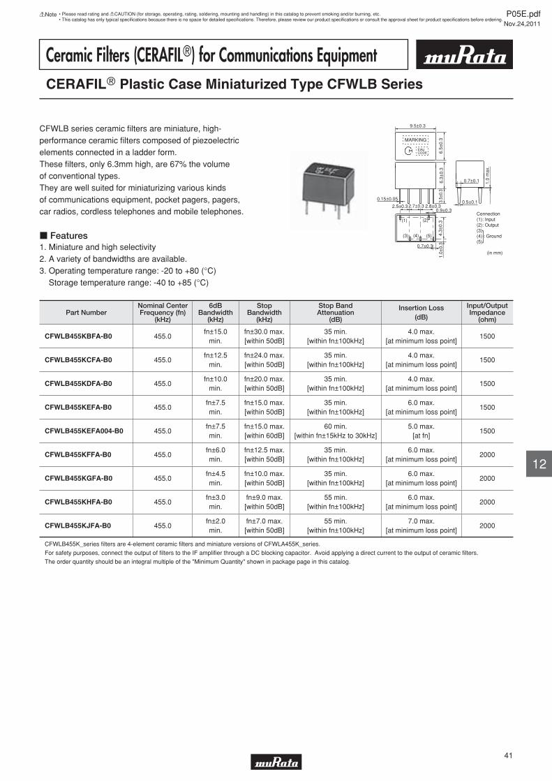
Ceramic Filters (CERAFILr) for Communications EquipmentCERAFILr Plastic Case Miniaturized Type CFWLB Series
CFWLB series ceramic fi lters are miniature, high-performance ceramic fi lters composed of piezoelectric elements connected in a ladder form.These fi lters, only 6.3mm high, are 67% the volume of conventional types.They are well suited for miniaturizing various kinds of communications equipment, pocket pagers, pagers, car radios, cordless telephones and mobile telephones.
c Features1. Miniature and high selectivity2. A variety of bandwidths are available.3. Operating temperature range: -20 to +80 (°C) Storage temperature range: -40 to +85 (°C)
4.3±
0.3
1.0
max
.
2.7±0.32.5±0.3
9.5±0.3
0.7±0.3
1.0±
0.3
6.3±
0.3
6.5±
0.3
0.5±0.1
0.7±0.1
3.5±
0.3
0.9±0.3
0.15±0.05
(1)
(3) (4)
(2)
(5)
2.8±0.3
Connection(1): Input(2): Output(3)(4) : Ground(5)
(in mm)
}
MARKING
EIAJCODE
Part NumberNominal CenterFrequency (fn)
(kHz)
6dBBandwidth
(kHz)
StopBandwidth
(kHz)
Stop BandAttenuation
(dB)
Insertion Loss(dB)
Input/OutputImpedance
(ohm)
CFWLB455KBFA-B0 455.0fn±15.0
min.fn±30.0 max.[within 50dB]
35 min.[within fn±100kHz]
4.0 max.[at minimum loss point]
1500
CFWLB455KCFA-B0 455.0fn±12.5
min.fn±24.0 max.[within 50dB]
35 min.[within fn±100kHz]
4.0 max.[at minimum loss point]
1500
CFWLB455KDFA-B0 455.0fn±10.0
min.fn±20.0 max.[within 50dB]
35 min.[within fn±100kHz]
4.0 max.[at minimum loss point]
1500
CFWLB455KEFA-B0 455.0fn±7.5min.
fn±15.0 max.[within 50dB]
35 min.[within fn±100kHz]
6.0 max.[at minimum loss point]
1500
CFWLB455KEFA004-B0 455.0fn±7.5min.
fn±15.0 max.[within 60dB]
60 min.[within fn±15kHz to 30kHz]
5.0 max.[at fn]
1500
CFWLB455KFFA-B0 455.0fn±6.0min.
fn±12.5 max.[within 50dB]
35 min.[within fn±100kHz]
6.0 max.[at minimum loss point]
2000
CFWLB455KGFA-B0 455.0fn±4.5min.
fn±10.0 max.[within 50dB]
35 min.[within fn±100kHz]
6.0 max.[at minimum loss point]
2000
CFWLB455KHFA-B0 455.0fn±3.0min.
fn±9.0 max.[within 50dB]
55 min.[within fn±100kHz]
6.0 max.[at minimum loss point]
2000
CFWLB455KJFA-B0 455.0fn±2.0min.
fn±7.0 max.[within 50dB]
55 min.[within fn±100kHz]
7.0 max.[at minimum loss point]
2000
CFWLB455K_series fi lters are 4-element ceramic fi lters and miniature versions of CFWLA455K_series.
For safety purposes, connect the output of fi lters to the IF amplifi er through a DC blocking capacitor. Avoid applying a direct current to the output of ceramic fi lters.
The order quantity should be an integral multiple of the "Minimum Quantity" shown in package page in this catalog.
P05E.pdfNov.24,2011
41
!Note • Please read rating and !CAUTION (for storage, operating, rating, soldering, mounting and handling) in this catalog to prevent smoking and/or burning, etc.• This catalog has only typical specifi cations because there is no space for detailed specifi cations. Therefore, please review our product specifi cations or consult the approval sheet for product specifi cations before ordering.
12
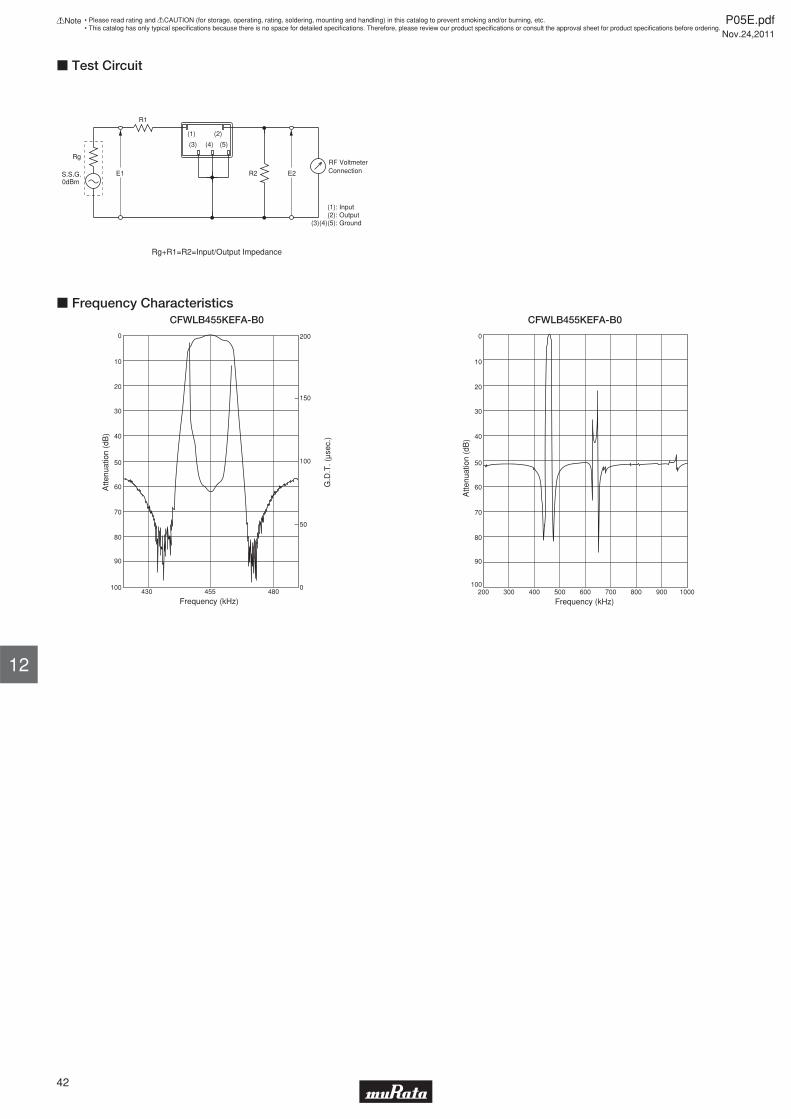
(1) (2)
(3) (4) (5)
R1
R2 E2E1
Rg
S.S.G.0dBm
RF VoltmeterConnection
(1)(2)
(3)(4)(5)
: Input: Output: Ground
Rg+R1=R2=Input/Output Impedance
c Test Circuit
100
40
30
20
10
0
Atte
nuat
ion
(dB
)
0
50
100
200
G.D
.T. (
μsec
.)
430 455 480
Frequency (kHz)
90
80
70
60
50
150
c Frequency CharacteristicsCFWLB455KEFA-B0
100
40
30
20
10
0
Atte
nuat
ion
(dB
)
200
Frequency (kHz)
90
80
70
60
50
300 400 500 600 700 800 900 1000
CFWLB455KEFA-B0
P05E.pdfNov.24,2011
42
!Note • Please read rating and !CAUTION (for storage, operating, rating, soldering, mounting and handling) in this catalog to prevent smoking and/or burning, etc.• This catalog has only typical specifi cations because there is no space for detailed specifi cations. Therefore, please review our product specifi cations or consult the approval sheet for product specifi cations before ordering.
12
Ceramic Filters (CERAFILr) for Communications EquipmentCERAFILr Plastic Case Group Delay Flat Type CFULA_Y Series
CFULA_Y series are high selectivity ceramic fi lters, which consist of 4 ceramic elements connected in a ladder form.They are most suitable for digital communications and cellular phones because of their improved GDT characteristics.
c Features1. High selectivity2. A variety of bandwidths are available.3. Excellent GDT characteristics are available within pass bandwidth.4. Easily mounted on a printed circuit board5. Operating temperature range: -20 to +80 (°C) Storage temperature range: -40 to +85 (°C)
3.0±
0.3
7.0±
0.3
4.2±
0.3
7.3±
0.3
0.8±0.1
0.6±0.11.2±0.5
8.0±0.3
MARKING
EIAJCODE
3.3±0.5
2.7±0.3
(1)(2)
(3)
0.3±
0.1
1.5
max
.
0.15±0.05
Connection(1): Input(2): Ground(3): Output
(in mm)
Part NumberCenter
Frequency (fo)(kHz)
6dBBandwidth
(kHz)
StopBandwidth
(kHz)
Stop BandAttenuation
(dB)
Insertion Loss(dB)
GDT Deviation(µs)
Input/OutputImpedance
(ohm)
CFULA455KB4Y-B0455
±1.5kHzfn±15.0
min.fn±35.0 max.[within 40dB]
25 min.[within fn±100kHz]
5.0 max.[at minimum loss point]
15.0 max.[within fn±10kHz]
1500
CFULA455KC4Y-B0455
±1.5kHzfn±12.5
min.fn±30.0 max.[within 40dB]
25 min.[within fn±100kHz]
6.0 max.[at minimum loss point]
15.0 max.[within fn±8kHz]
1500
CFULA455KD1Y-B0455
±1.0kHzfn±10.0
min.fn±25.0 max.[within 40dB]
23 min.[within fn±100kHz]
7.0 max.[at minimum loss point]
20.0 max.[within fn±7kHz]
1500
CFULA455KE1Y-B0455
±1.0kHzfn±7.5min.
fn±20.0 max.[within 40dB]
23 min.[within fn±100kHz]
8.0 max.[at minimum loss point]
20.0 max.[within fn±5kHz]
1500
CFULA455KF1Y-B0455
±1.0kHzfn±6.0min.
fn±17.5 max.[within 40dB]
23 min.[within fn±100kHz]
9.0 max.[at minimum loss point]
20.0 max.[within fn±4kHz]
2000
CFULA455KG1Y-B0455
±1.0kHzfn±4.5min.
fn±15.0 max.[within 40dB]
23 min.[within fn±100kHz]
10.0 max.[at minimum loss point]
20.0 max.[within fn±3kHz]
2000
Center frequency (fo) defi ned by the center of 6dB bandwidth.
(fn) means nominal center frequency 455kHz.
For safety purposes, connect the output of fi lters to the IF amplifi er through a DC blocking capacitor. Avoid applying a direct current to the output of ceramic fi lters.
The order quantity should be an integral multiple of the "Minimum Quantity" shown in package page in this catalog.
E1
R1
Rg
S.S.G.0dBm
R2 E2 RF Voltmeter Connection
(1): Input
(2): Ground
(3): Output
(1) (2)(3)
Rg+R1=R2=Input/Output Impedance
c Test Circuit
P05E.pdfNov.24,2011
43
!Note • Please read rating and !CAUTION (for storage, operating, rating, soldering, mounting and handling) in this catalog to prevent smoking and/or burning, etc.• This catalog has only typical specifi cations because there is no space for detailed specifi cations. Therefore, please review our product specifi cations or consult the approval sheet for product specifi cations before ordering.
13
Atte
nuat
ion
(dB
)
Frequency (kHz)
Gro
up D
elay
Tim
e (μ
sec)
430 455 480
10
20
30
40
50
60
70
80
90
100
200
150
100
50
0
0
c Frequency CharacteristicsCFULA455KE1Y-B0
200 300 400 500 600 700 800 900 1000
10
20
30
40
50
60
70
80
90
Atte
nuat
ion
(dB
)
Frequency (kHz)
0
100
CFULA455KE1Y-B0
P05E.pdfNov.24,2011
44
!Note • Please read rating and !CAUTION (for storage, operating, rating, soldering, mounting and handling) in this catalog to prevent smoking and/or burning, etc.• This catalog has only typical specifi cations because there is no space for detailed specifi cations. Therefore, please review our product specifi cations or consult the approval sheet for product specifi cations before ordering.
13
Ceramic Filters (CERAFILr) for Communications EquipmentCERAFILr Plastic Case Group Delay Flat Type CFWLA_Y Series
CFWLA_Y series are high selectivity ceramic fi lters, which consist of 6 ceramic elements connected in a ladder form.They are most suitable for digital communications and mobile telephones because of their improved GDT characteristics.
c Features1. High selectivity2. A variety of bandwidths are available3. Excellent GDT characteristics are available within pass bandwidth.4. Easily mounted on a printed circuit board5. Operating temperature range: -20 to +80 (°C) Storage temperature range: -40 to +85 (°C)
4.3±
0.3
0.15
1.5
max
.
2.3±0.5 2.0±0.3
2.9±0.3
11.0±0.5
MARKING
EIAJCODE
1.2±0.5
(1)(2)(4) (3)
(5)
1.35
±0.
5
7.0±
0.5
3.5±
0.5
0.6±0.1
0.8±0.17.5±
0.5
2.6±0.3
Connection (1): Input(2)(3)(4): Ground (5): Output
(in mm)
2.9—0.32.9±0.3
Part NumberCenter
Frequency (fo)(kHz)
6dBBandwidth
(kHz)
StopBandwidth
(kHz)
Stop BandAttenuation
(dB)
Insertion Loss(dB)
GDT Deviation(µs)
Input/OutputImpedance
(ohm)
CFWLA455KB4Y-B0455
±1.5kHzfn±15.0
min.fn±30.0 max.[within 50dB]
40 min.[within fn±100kHz]
6.0 max.[at minimum loss point]
30.0 max.[within fn±10kHz]
1500
CFWLA455KC4Y-B0455
±1.5kHzfn±12.5
min.fn±27.5 max.[within 50dB]
40 min.[within fn±100kHz]
7.0 max.[at minimum loss point]
30.0 max.[within fn±8kHz]
1500
CFWLA455KD1Y-B0455
±1.0kHzfn±10.0
min.fn±25.0 max.[within 50dB]
40 min.[within fn±100kHz]
8.0 max.[at minimum loss point]
30.0 max.[within fn±7kHz]
1500
CFWLA455KE1Y-B0455
±1.0kHzfn±7.5min.
fn±20.0 max.[within 50dB]
40 min.[within fn±100kHz]
9.0 max.[at minimum loss point]
30.0 max.[within fn±5kHz]
1500
CFWLA455KF1Y-B0455
±1.0kHzfn±6.0min.
fn±17.5 max.[within 50dB]
40 min.[within fn±100kHz]
10.0 max.[at minimum loss point]
40.0 max.[within fn±4kHz]
2000
CFWLA455KG1Y-B0455
±1.0kHzfn±4.5min.
fn±15.0 max.[within 50dB]
40 min.[within fn±100kHz]
11.0 max.[at minimum loss point]
40.0 max.[within fn±3kHz]
2000
Center frequency (fo) defi ned by the center of 6dB bandwidth.
(fn) means nominal center frequency 455kHz.
For safety purposes, connect the output of fi lters to the IF amplifi er through a DC blocking capacitor. Avoid applying a direct current to the output of ceramic fi lters.
The order quantity should be an integral multiple of the "Minimum Quantity" shown in package page in this catalog.
E1
R1
R2 E2 RF Voltmeter Connection (1): Input
(5): Output
(2)(3)(4): Ground
Rg
S.S.G.0dBm
(1) (2) (3) (4)
(5)
Rg+R1=R2=Input/Output Impedance
c Test Circuit
P05E.pdfNov.24,2011
45
!Note • Please read rating and !CAUTION (for storage, operating, rating, soldering, mounting and handling) in this catalog to prevent smoking and/or burning, etc.• This catalog has only typical specifi cations because there is no space for detailed specifi cations. Therefore, please review our product specifi cations or consult the approval sheet for product specifi cations before ordering.
14
Atte
nuat
ion
(dB
)
430 455 480
Frequency (kHz)
10
20
30
40
50
60
70
80
90
100
400
300
200
100
0
Gro
up D
elay
Tim
e (μ
sec)
0
c Frequency CharacteristicsCFWLA455KE1Y-B0
200 300 400 500 600 700 800 900 1000
10
20
30
40
50
60
70
80
90
Atte
nuat
ion
(dB
)
Frequency (kHz)
0
100
CFWLA455KE1Y-B0
P05E.pdfNov.24,2011
46
!Note • Please read rating and !CAUTION (for storage, operating, rating, soldering, mounting and handling) in this catalog to prevent smoking and/or burning, etc.• This catalog has only typical specifi cations because there is no space for detailed specifi cations. Therefore, please review our product specifi cations or consult the approval sheet for product specifi cations before ordering.
14
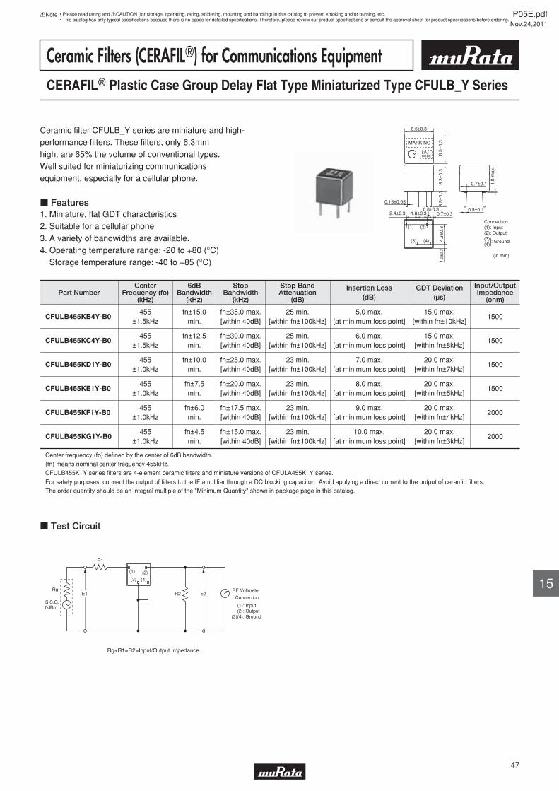
Ceramic Filters (CERAFILr) for Communications EquipmentCERAFILr Plastic Case Group Delay Flat Type Miniaturized Type CFULB_Y Series
Ceramic fi lter CFULB_Y series are miniature and high-performance fi lters. These fi lters, only 6.3mm high, are 65% the volume of conventional types.Well suited for miniaturizing communications equipment, especially for a cellular phone.
c Features1. Miniature, fl at GDT characteristics2. Suitable for a cellular phone3. A variety of bandwidths are available.4. Operating temperature range: -20 to +80 (°C) Storage temperature range: -40 to +85 (°C)
4.3±
0.3
1.0
max
.
1.8±0.32.4±0.3
6.5±0.3
0.8±0.3
1.0±
0.3
6.3±
0.3
6.5±
0.3
0.5±0.1
0.7±0.1
3.5±
0.3
0.7±0.3
(1) (2)
(3) (4)
0.15±0.05
Connection(1): Input(2): Output(3)
: Ground(4)
(in mm)
}
MARKING
EIAJCODE
Part NumberCenter
Frequency (fo)(kHz)
6dBBandwidth
(kHz)
StopBandwidth
(kHz)
Stop BandAttenuation
(dB)
Insertion Loss(dB)
GDT Deviation(µs)
Input/OutputImpedance
(ohm)
CFULB455KB4Y-B0455
±1.5kHzfn±15.0
min.fn±35.0 max.[within 40dB]
25 min.[within fn±100kHz]
5.0 max.[at minimum loss point]
15.0 max.[within fn±10kHz]
1500
CFULB455KC4Y-B0455
±1.5kHzfn±12.5
min.fn±30.0 max.[within 40dB]
25 min.[within fn±100kHz]
6.0 max.[at minimum loss point]
15.0 max.[within fn±8kHz]
1500
CFULB455KD1Y-B0455
±1.0kHzfn±10.0
min.fn±25.0 max.[within 40dB]
23 min.[within fn±100kHz]
7.0 max.[at minimum loss point]
20.0 max.[within fn±7kHz]
1500
CFULB455KE1Y-B0455
±1.0kHzfn±7.5min.
fn±20.0 max.[within 40dB]
23 min.[within fn±100kHz]
8.0 max.[at minimum loss point]
20.0 max.[within fn±5kHz]
1500
CFULB455KF1Y-B0455
±1.0kHzfn±6.0min.
fn±17.5 max.[within 40dB]
23 min.[within fn±100kHz]
9.0 max.[at minimum loss point]
20.0 max.[within fn±4kHz]
2000
CFULB455KG1Y-B0455
±1.0kHzfn±4.5min.
fn±15.0 max.[within 40dB]
23 min.[within fn±100kHz]
10.0 max.[at minimum loss point]
20.0 max.[within fn±3kHz]
2000
Center frequency (fo) defi ned by the center of 6dB bandwidth.
(fn) means nominal center frequency 455kHz.
CFULB455K_Y series fi lters are 4-element ceramic fi lters and miniature versions of CFULA455K_Y series.
For safety purposes, connect the output of fi lters to the IF amplifi er through a DC blocking capacitor. Avoid applying a direct current to the output of ceramic fi lters.
The order quantity should be an integral multiple of the "Minimum Quantity" shown in package page in this catalog.
E1
R1
Rg
S.S.G.0dBm
R2 E2RF Voltmeter
Connection
(1)(2)
(3)(4)
: Input: Output: Ground
(1) (2)(3) (4)
Rg+R1=R2=Input/Output Impedance
c Test Circuit
P05E.pdfNov.24,2011
47
!Note • Please read rating and !CAUTION (for storage, operating, rating, soldering, mounting and handling) in this catalog to prevent smoking and/or burning, etc.• This catalog has only typical specifi cations because there is no space for detailed specifi cations. Therefore, please review our product specifi cations or consult the approval sheet for product specifi cations before ordering.
15
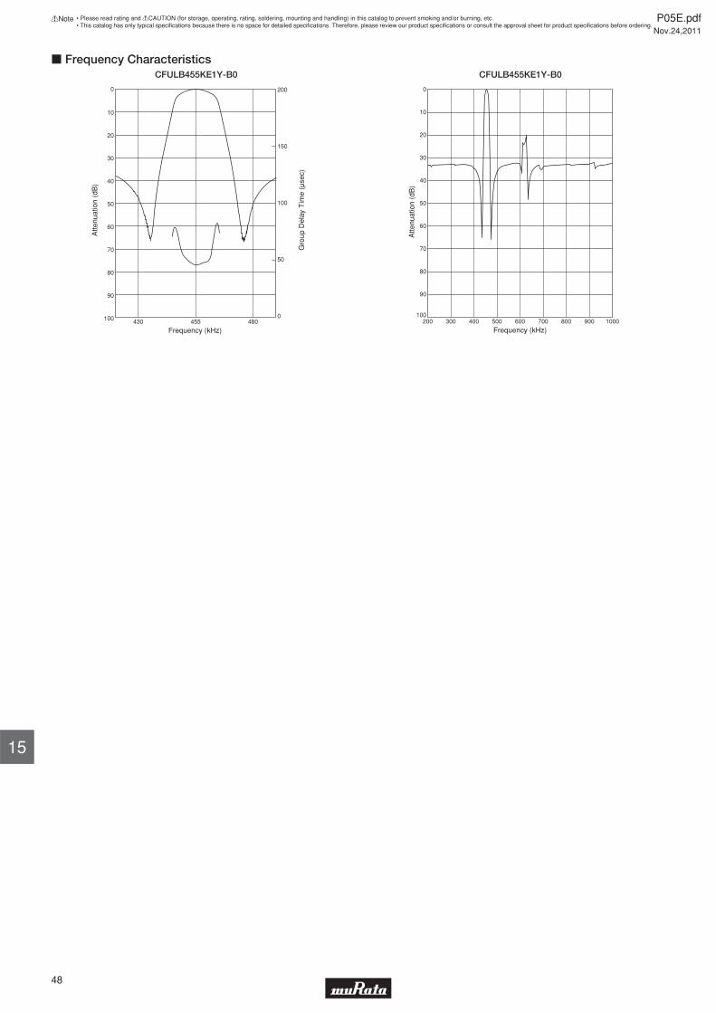
Atte
nuat
ion
(dB
)
Frequency (kHz)
Gro
up D
elay
Tim
e (μ
sec)
430 455 480
10
20
30
40
50
60
70
80
90
100
200
150
100
50
0
0
c Frequency CharacteristicsCFULB455KE1Y-B0
200 300 400 500 600 700 800 900 1000
10
20
30
40
50
60
70
80
90
Atte
nuat
ion
(dB
)
Frequency (kHz)
0
100
CFULB455KE1Y-B0
P05E.pdfNov.24,2011
48
!Note • Please read rating and !CAUTION (for storage, operating, rating, soldering, mounting and handling) in this catalog to prevent smoking and/or burning, etc.• This catalog has only typical specifi cations because there is no space for detailed specifi cations. Therefore, please review our product specifi cations or consult the approval sheet for product specifi cations before ordering.
15
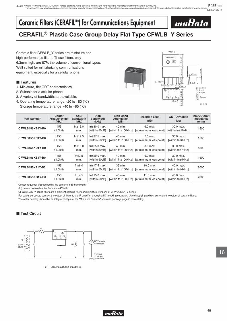
Ceramic Filters (CERAFILr) for Communications EquipmentCERAFILr Plastic Case Group Delay Flat Type CFWLB_Y Series
Ceramic fi lter CFWLB_Y series are miniature andhigh-performance fi lters. These fi lters, only 6.3mm high, are 67% the volume of conventional types.Well suited for miniaturizing communications equipment, especially for a cellular phone.
c Features1. Miniature, fl at GDT characteristics2. Suitable for a cellular phone3. A variety of bandwidths are available.4. Operating temperature range: -20 to +80 (°C) Storage temperature range: -40 to +85 (°C)
4.3±
0.3
1.0
max
.
2.7±0.32.5±0.3
9.5±0.3
0.7±0.3
1.0±
0.3
6.3±
0.3
6.5±
0.3
0.5±0.1
0.7±0.1
3.5±
0.3
0.9±0.3
0.15±0.05
(1)
(3) (4)
(2)
(5)
2.8±0.3
Connection(1): Input(2): Output(3)(4) : Ground(5)
(in mm)
}
MARKING
EIAJCODE
Part NumberCenter
Frequency (fo)(kHz)
6dBBandwidth
(kHz)
StopBandwidth
(kHz)
Stop BandAttenuation
(dB)
Insertion Loss(dB)
GDT Deviation(µs)
Input/OutputImpedance
(ohm)
CFWLB455KB4Y-B0455
±1.5kHzfn±15.0
min.fn±30.0 max.[within 50dB]
40 min.[within fn±100kHz]
6.0 max.[at minimum loss point]
30.0 max.[within fn±10kHz]
1500
CFWLB455KC4Y-B0455
±1.5kHzfn±12.5
min.fn±27.5 max.[within 50dB]
40 min.[within fn±100kHz]
7.0 max.[at minimum loss point]
30.0 max.[within fn±8kHz]
1500
CFWLB455KD1Y-B0455
±1.0kHzfn±10.0
min.fn±25.0 max.[within 50dB]
40 min.[within fn±100kHz]
8.0 max.[at minimum loss point]
30.0 max.[within fn±7kHz]
1500
CFWLB455KE1Y-B0455
±1.0kHzfn±7.5min.
fn±20.0 max.[within 50dB]
40 min.[within fn±100kHz]
9.0 max.[at minimum loss point]
30.0 max.[within fn±5kHz]
1500
CFWLB455KF1Y-B0455
±1.0kHzfn±6.0min.
fn±17.5 max.[within 50dB]
35 min.[within fn±100kHz]
10.0 max.[at minimum loss point]
40.0 max.[within fn±4kHz]
2000
CFWLB455KG1Y-B0455
±1.0kHzfn±4.5min.
fn±15.0 max.[within 50dB]
40 min.[within fn±100kHz]
11.0 max.[at minimum loss point]
40.0 max.[within fn±3kHz]
2000
Center frequency (fo) defi ned by the center of 6dB bandwidth.
(fn) means nominal center frequency 455kHz.
CFWLB455K_Y series fi lters are 4-element ceramic fi lters and miniature versions of CFWLA455K_Y series.
For safety purposes, connect the output of fi lters to the IF amplifi er through a DC blocking capacitor. Avoid applying a direct current to the output of ceramic fi lters.
The order quantity should be an integral multiple of the "Minimum Quantity" shown in package page in this catalog.
(1) (2)
(3) (4) (5)
R1
R2 E2E1
Rg
S.S.G.0dBm
RF VoltmeterConnection
(1)(2)
(3)(4)(5)
: Input: Output: Ground
Rg+R1=R2=Input/Output Impedance
c Test Circuit
P05E.pdfNov.24,2011
49
!Note • Please read rating and !CAUTION (for storage, operating, rating, soldering, mounting and handling) in this catalog to prevent smoking and/or burning, etc.• This catalog has only typical specifi cations because there is no space for detailed specifi cations. Therefore, please review our product specifi cations or consult the approval sheet for product specifi cations before ordering.
16
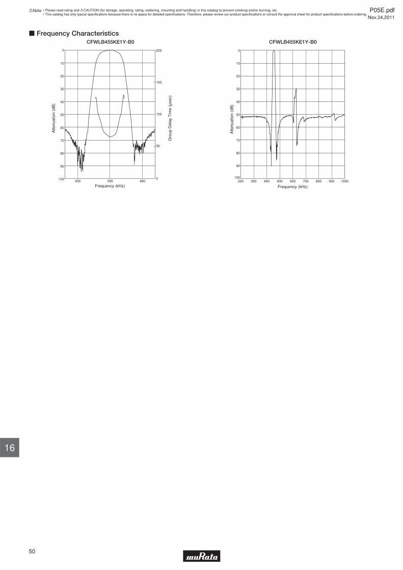
Atte
nuat
ion
(dB
)
430 455 480
Frequency (kHz)
10
20
30
40
50
60
70
80
90
100
200
150
100
50
0
Gro
up D
elay
Tim
e (μ
sec)
0
c Frequency CharacteristicsCFWLB455KE1Y-B0
200 300 400 500 600 700 800 900 1000
10
20
30
40
50
60
70
80
90
Atte
nuat
ion
(dB
)
Frequency (kHz)
0
100
CFWLB455KE1Y-B0
P05E.pdfNov.24,2011
50
!Note • Please read rating and !CAUTION (for storage, operating, rating, soldering, mounting and handling) in this catalog to prevent smoking and/or burning, etc.• This catalog has only typical specifi cations because there is no space for detailed specifi cations. Therefore, please review our product specifi cations or consult the approval sheet for product specifi cations before ordering.
16
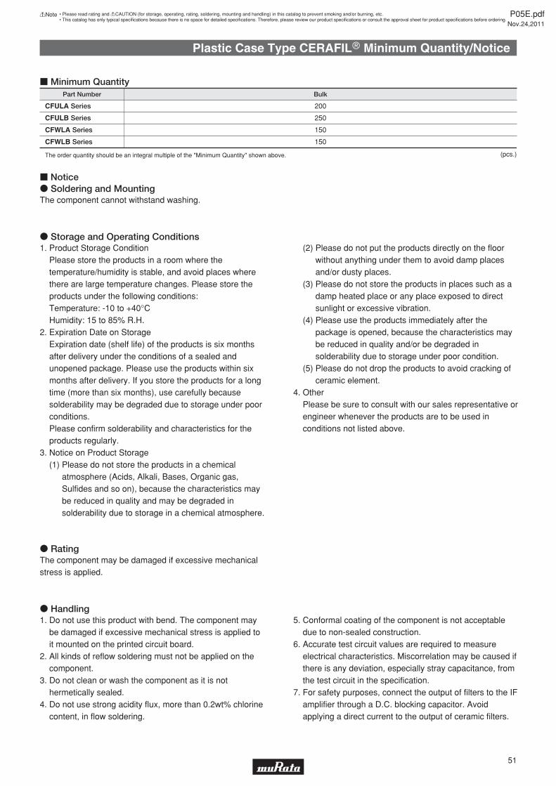
Plastic Case Type CERAFILr Minimum Quantity/Notice
Part Number Bulk
200
250
150
150
CFULA Series
CFULB Series
CFWLA Series
CFWLB Series
(pcs.)The order quantity should be an integral multiple of the "Minimum Quantity" shown above.
c Minimum Quantity
o Storage and Operating Conditions
o RatingThe component may be damaged if excessive mechanical stress is applied.
o Soldering and MountingThe component cannot withstand washing.
o Handling1. Do not use this product with bend. The component may
be damaged if excessive mechanical stress is applied to it mounted on the printed circuit board.
2. All kinds of reflow soldering must not be applied on the component.
3. Do not clean or wash the component as it is not hermetically sealed.
4. Do not use strong acidity flux, more than 0.2wt% chlorine content, in flow soldering.
5. Conformal coating of the component is not acceptable due to non-sealed construction.
6. Accurate test circuit values are required to measure electrical characteristics. Miscorrelation may be caused if there is any deviation, especially stray capacitance, from the test circuit in the specification.
7. For safety purposes, connect the output of filters to the IF amplifier through a D.C. blocking capacitor. Avoid applying a direct current to the output of ceramic filters.
1. Product Storage ConditionPlease store the products in a room where the temperature/humidity is stable, and avoid places where there are large temperature changes. Please store the products under the following conditions: Temperature: -10 to +40°CHumidity: 15 to 85% R.H.
2. Expiration Date on StorageExpiration date (shelf life) of the products is six months after delivery under the conditions of a sealed and unopened package. Please use the products within six months after delivery. If you store the products for a long time (more than six months), use carefully because solderability may be degraded due to storage under poor conditions.Please confirm solderability and characteristics for the products regularly.
3. Notice on Product Storage(1) Please do not store the products in a chemical
atmosphere (Acids, Alkali, Bases, Organic gas, Sulfides and so on), because the characteristics may be reduced in quality and may be degraded in solderability due to storage in a chemical atmosphere.
(2) Please do not put the products directly on the floor without anything under them to avoid damp places and/or dusty places.
(3) Please do not store the products in places such as a damp heated place or any place exposed to direct sunlight or excessive vibration.
(4) Please use the products immediately after the package is opened, because the characteristics may be reduced in quality and/or be degraded in solderability due to storage under poor condition.
(5) Please do not drop the products to avoid cracking of ceramic element.
4. OtherPlease be sure to consult with our sales representative or engineer whenever the products are to be used in conditions not listed above.
c Notice
P05E.pdfNov.24,2011
51
!Note • Please read rating and !CAUTION (for storage, operating, rating, soldering, mounting and handling) in this catalog to prevent smoking and/or burning, etc.• This catalog has only typical specifi cations because there is no space for detailed specifi cations. Therefore, please review our product specifi cations or consult the approval sheet for product specifi cations before ordering.
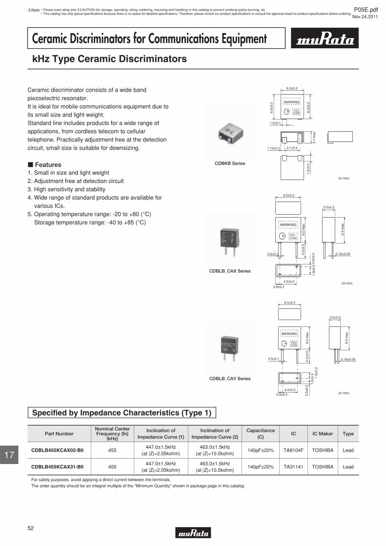
Ceramic Discriminators for Communications EquipmentkHz Type Ceramic Discriminators
Ceramic discriminator consists of a wide band piezoelectric resonator.It is ideal for mobile communications equipment due toits small size and light weight.Standard line includes products for a wide range of applications, from cordless telecom to cellular telephone. Practically adjustment free at the detectioncircuit, small size is suitable for downsizing.
c Features 1. Small in size and light weight2. Adjustment free at detection circuit3. High sensitivity and stability4. Wide range of standard products are available for various ICs.5. Operating temperature range: -20 to +80 (°C) Storage temperature range: -40 to +85 (°C)
MARKING
EIAJCODE6.
6±0.
3
1.5±
0.3
6.0±0.2
1.15±0.2
1.0±0.1
3.7±0.2
3.1
max
.
6.2±
0.2
(in mm)
CDBKB Series
(in mm)
MARKING
EIAJCODE
0.6±
0.2
1.8±
0.2
6.3
max
.
4.2±0.2
6.0±0.2
0.5±0.1 0.15±0.05
0.9±0.2
3.0±0.3
6.0
max
.4.
2±0.
5
CDBLB_CAX Series
(in mm)
MARKING
EIAJCODE
1.5±
0.3
1.0±
0.3
0.5±
0.2
6.3
max
.
4.2±0.2
6.0±0.2
0.5±0.1 0.15±0.05
0.9±0.2
3.0±0.3
6.0
max
.4.
2±0.
5
CDBLB_CAY Series
Specifi ed by Impedance Characteristics (Type 1)
Part NumberNominal CenterFrequency (fn)
(kHz)
Inclination ofImpedance Curve (1)
Inclination ofImpedance Curve (2)
Capacitance(C)
IC IC Maker Type
CDBLB455KCAX02-B0 455447.0±1.5kHz
(at |Z|=2.05kohm)463.0±1.5kHz
(at |Z|=10.0kohm)140pF±20% TA8104F TOSHIBA Lead
CDBLB455KCAX31-B0 455447.0±1.5kHz
(at |Z|=2.05kohm)463.0±1.5kHz
(at |Z|=10.0kohm)140pF±20% TA31141 TOSHIBA Lead
For safety purposes, avoid applying a direct current between the terminals.
The order quantity should be an integral multiple of the "Minimum Quantity" shown in package page in this catalog.
P05E.pdfNov.24,2011
52
!Note • Please read rating and !CAUTION (for storage, operating, rating, soldering, mounting and handling) in this catalog to prevent smoking and/or burning, etc.• This catalog has only typical specifi cations because there is no space for detailed specifi cations. Therefore, please review our product specifi cations or consult the approval sheet for product specifi cations before ordering.
17
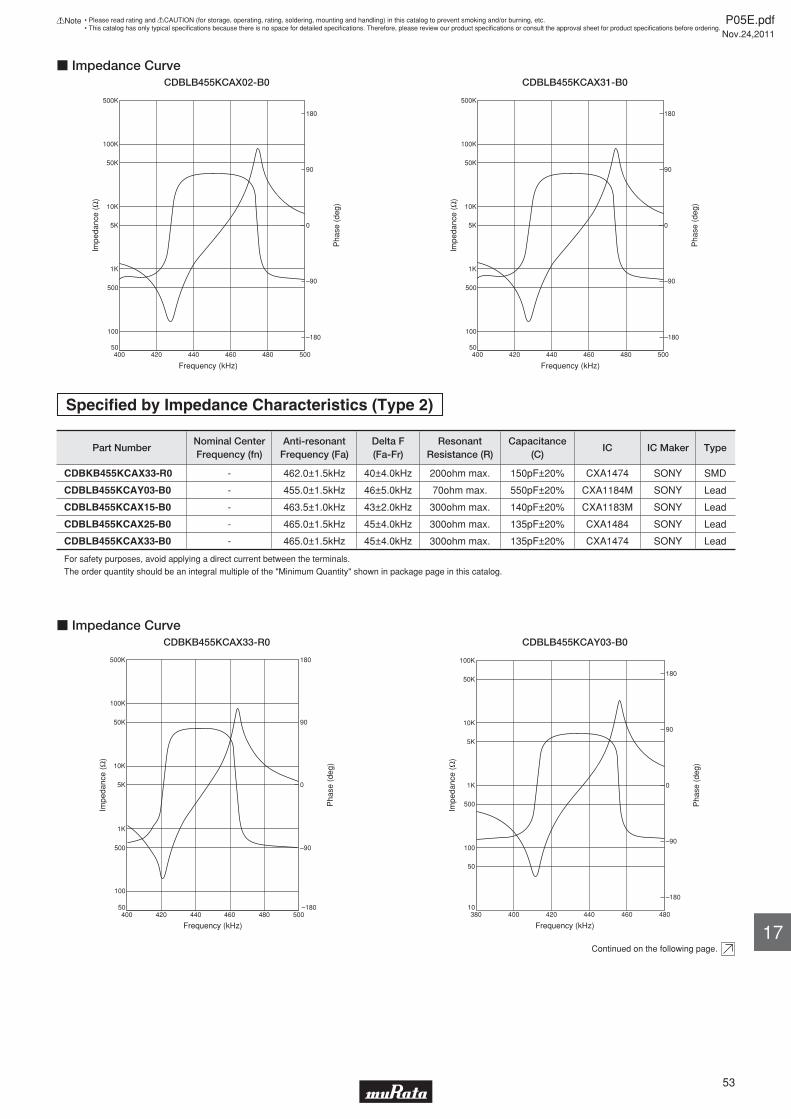
500K
180
50K90
10K
5K 0
1K
500–90
100–180
Impe
danc
e (Ω
)
Pha
se (
deg)
400 420 440 460 480
Frequency (kHz)
500
100K
50
c Impedance CurveCDBLB455KCAX02-B0
500K
180
50K90
10K
5K 0
1K
500–90
100–180
Impe
danc
e (Ω
)
Pha
se (
deg)
400 420 440 460 480
Frequency (kHz)
500
100K
50
CDBLB455KCAX31-B0
Specifi ed by Impedance Characteristics (Type 2)
Part NumberNominal CenterFrequency (fn)
Anti-resonantFrequency (Fa)
Delta F(Fa-Fr)
ResonantResistance (R)
Capacitance(C)
IC IC Maker Type
CDBKB455KCAX33-R0 - 462.0±1.5kHz 40±4.0kHz 200ohm max. 150pF±20% CXA1474 SONY SMD
CDBLB455KCAY03-B0 - 455.0±1.5kHz 46±5.0kHz 70ohm max. 550pF±20% CXA1184M SONY Lead
CDBLB455KCAX15-B0 - 463.5±1.0kHz 43±2.0kHz 300ohm max. 140pF±20% CXA1183M SONY Lead
CDBLB455KCAX25-B0 - 465.0±1.5kHz 45±4.0kHz 300ohm max. 135pF±20% CXA1484 SONY Lead
CDBLB455KCAX33-B0 - 465.0±1.5kHz 45±4.0kHz 300ohm max. 135pF±20% CXA1474 SONY Lead
For safety purposes, avoid applying a direct current between the terminals.
The order quantity should be an integral multiple of the "Minimum Quantity" shown in package page in this catalog.
Continued on the following page.
500K
100K
10K
Impe
danc
e (Ω
)
Pha
se (
deg)
400 420 440 460 480 500
Frequency (kHz)
500
50
180
50K 90
5K 0
–90
1K
–180
100
c Impedance CurveCDBKB455KCAX33-R0
100K
180
5K
90
1K
500
0
100
50
–90
–180
Impe
danc
e (Ω
)
380 400 420 440 460
Frequency (kHz)
480
10K
10
50K
Pha
se (
deg)
CDBLB455KCAY03-B0
P05E.pdfNov.24,2011
53
!Note • Please read rating and !CAUTION (for storage, operating, rating, soldering, mounting and handling) in this catalog to prevent smoking and/or burning, etc.• This catalog has only typical specifi cations because there is no space for detailed specifi cations. Therefore, please review our product specifi cations or consult the approval sheet for product specifi cations before ordering.
17
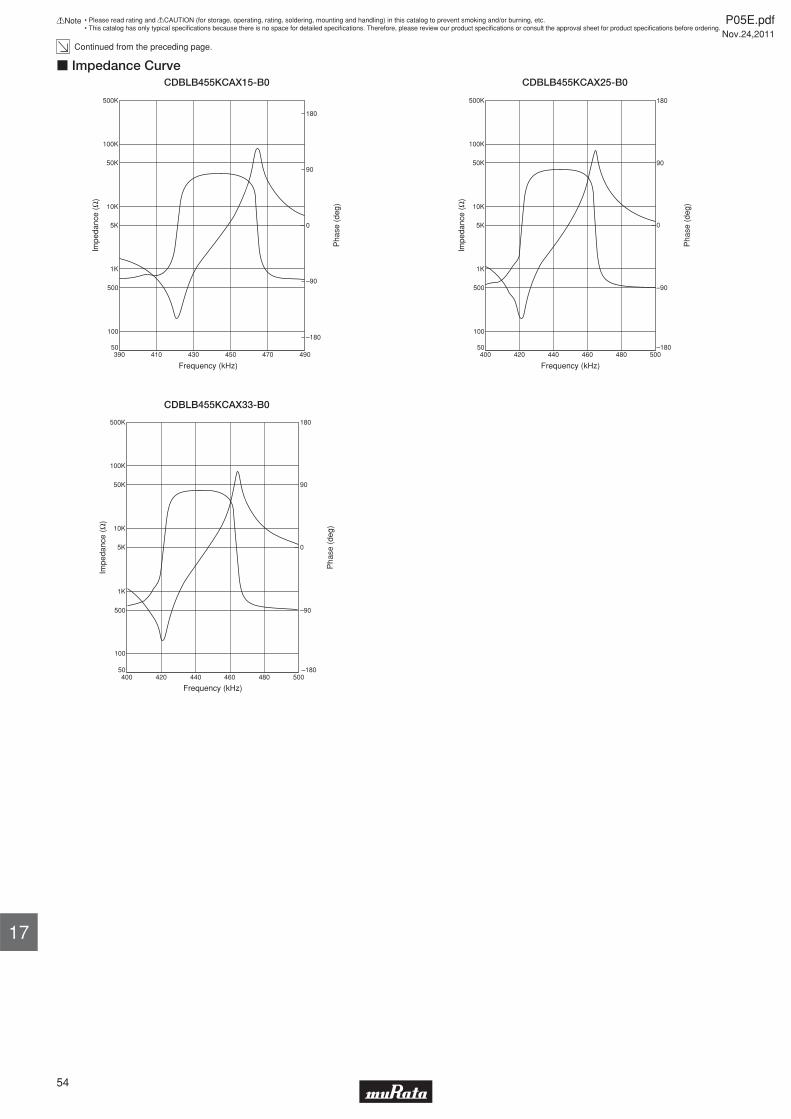
Continued from the preceding page.
500K
180
50K90
10K
5K 0
1K
500–90
100–180
Impe
danc
e (Ω
)
Pha
se (
deg)
390 410 430 450 470
Frequency (kHz)
490
100K
50
c Impedance CurveCDBLB455KCAX15-B0
500K 180
50K 90
10K
5K 0
1K
500 –90
100
–180
Impe
danc
e (Ω
)
Pha
se (
deg)
400 420 440 460 480
Frequency (kHz)
500
100K
50
CDBLB455KCAX25-B0
500K
100K
10K
Impe
danc
e (Ω
)
Pha
se (
deg)
400 420 440 460 480 500
Frequency (kHz)
500
50
180
50K 90
5K 0
–90
1K
–180
100
CDBLB455KCAX33-B0
P05E.pdfNov.24,2011
54
!Note • Please read rating and !CAUTION (for storage, operating, rating, soldering, mounting and handling) in this catalog to prevent smoking and/or burning, etc.• This catalog has only typical specifi cations because there is no space for detailed specifi cations. Therefore, please review our product specifi cations or consult the approval sheet for product specifi cations before ordering.
17
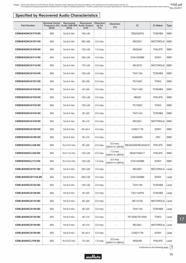
Specifi ed by Recovered Audio Characteristics
Part NumberNominal CenterFrequency (fn)
(kHz)
RecoveredAudio 3dB BW
(kHz)
RecoveredAudio Output
(mV)
Distortion(at fn)(%)
Distortion(%)
IC IC Maker Type
CDBKB450KCAY79-R0 450 fn±3.0 min. 145 ±40 - - TB32302FG TOSHIBA SMD
CDBKB455KCAY07-R0 455 fn±4.0 min. 350 ±60 3.0 max. - MC3357 MOTOROLA SMD
CDBKB455KCAY09-R0 455 fn±4.0 min. 120 ±40 1.5 max. - NE604N PHILIPS SMD
CDBKB455KCAY13-R0 455 fn±4.0 min. 330 ±50 4.0 max. - CXA1003BM SONY SMD
CDBKB455KCAY16-R0 455 fn±4.0 min. 175 ±40 2.0 max. - MC3372 MOTOROLA SMD
CDBKB455KCAY24-R0 455 fn±4.0 min. 100 ±40 2.0 max. - TA31136 TOSHIBA SMD
CDBKB455KCAY27-R0 455 fn±4.0 min. 90 ±30 2.0 max. - TK10487 TOKO SMD
CDBKB455KCAY28-R0 455 fn±4.0 min. 40 ±20 3.0 max. - TA31142F TOSHIBA SMD
CDBKB455KCAY29-R0 455 fn±4.0 min. 100 ±30 2.5 max. - NE605 PHILIPS SMD
CDBKB455KCAY35-R0 455 fn±4.0 min. 100 ±40 2.5 max. - TK10930 TOKO SMD
CDBKB455KCAY40-R0 455 fn±4.0 min. 40 ±20 3.5 max. - TA31145 TOSHIBA SMD
CDBKB455KCAY49-R0 455 fn±4.0 min. 45 ±10 3.0 max. - MC3361 MOTOROLA SMD
CDBKB455KCAY50-R0 455 fn±4.0 min. 64 ±6.4 4.0 max. - CXA3117N SONY SMD
CDBKB455KCAY66-R0 455 fn±4.2 min. 40 ±10 4.0 max. - NJM2590 JRC SMD
CDBKB455KCLX36-R0 455 fn±13.0 min. 90 ±30 2.5 max.5.0 max.
[within fn ±6kHz]NE(SA)606/NE(SA)616 PHILIPS SMD
CDBKB455KCLX39-R0 455 fn±11.0 min. 130 ±20 2.5 max.7.0 max.
[within fn ±8kHz]NE607/NE617 PHILIPS SMD
CDBKB455KCLY13-R0 455 fn±13.0 min. 120 ±30 1.5 max.5.0 max.
[within fn ±8kHz]CXA1003BM SONY SMD
CDBLB455KCAY07-B0 455 fn±4.0 min. 340 ±60 3.0 max. - MC3357 MOTOROLA Lead
CDBLB455KCAY13A-B0 455 fn±4.0 min. 350 ±50 3.0 max. - CXA1003BM SONY Lead
CDBLB455KCAY24-B0 455 fn±4.0 min. 100 ±40 2.0 max. - TA31136 TOSHIBA Lead
CDBLB455KCAY28-B0 455 fn±4.0 min. 40 ±20 3.0 max. - TA31142FN TOSHIBA Lead
CDBLB455KCAY34-B0 455 fn±4.0 min. 65 ±20 2.5 max. - MC13136 MOTOROLA Lead
CDBLB455KCAY40-B0 455 fn±4.0 min. 40 ±20 3.0 max. - TA31145 TOSHIBA Lead
CDBLB455KCAY42-B0 455 fn±4.0 min. 40 ±15 3.0 max. - TK14590/TK14591 TOKO Lead
CDBLB455KCAY49-B0 455 fn±4.0 min. 45 ±10 3.0 max. - MC3361 MOTOROLA Lead
CDBLB455KCAY50-B0 455 fn±4.0 min. 64 ±6.4 4.0 max. - CXA3117N SONY Lead
CDBLB455KCLY09-B0 455 fn±15.0 min. 70 ±20 1.5 max.3.5 max.
[within fn ±8kHz]NE604N PHILIPS Lead
Continued on the following page.
P05E.pdfNov.24,2011
55
!Note • Please read rating and !CAUTION (for storage, operating, rating, soldering, mounting and handling) in this catalog to prevent smoking and/or burning, etc.• This catalog has only typical specifi cations because there is no space for detailed specifi cations. Therefore, please review our product specifi cations or consult the approval sheet for product specifi cations before ordering.
17
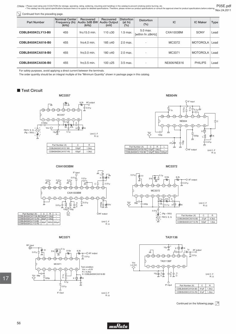
Continued from the preceding page.
Part NumberNominal CenterFrequency (fn)
(kHz)
RecoveredAudio 3dB BW
(kHz)
RecoveredAudio Output
(mV)
Distortion(at fn)(%)
Distortion(%)
IC IC Maker Type
CDBLB455KCLY13-B0 455 fn±15.0 min. 110 ±30 1.5 max.5.0 max.
[within fn ±8kHz]CXA1003BM SONY Lead
CDBLB455KCAX16-B0 455 fn±4.0 min. 185 ±40 2.0 max. - MC3372 MOTOROLA Lead
CDBLB455KCAX18-B0 455 fn±3.0 min. 180 ±40 2.0 max. - MC3371 MOTOROLA Lead
CDBLB455KCAX36-B0 455 fn±3.5 min. 100 ±25 3.5 max. - NE606/NE616 PHILIPS Lead
For safety purposes, avoid applying a direct current between the terminals.
The order quantity should be an integral multiple of the "Minimum Quantity" shown in package page in this catalog.
AF output
Vcc
0.1μ
0.01μ
C
RX
0.022μ
FM S. S. G.(Rg = 50Ω)
16 915 14 13 12 11 10
1 82 3 4 5 6 7
8.2k10k
MC3357
50
0.1μ+10μ
47k
CDBLB455KCAY07-B0
CDBKB455KCAY07-R0
Part Number (X) C R
150pF
150pF
1.5kΩ
1.3kΩ
Unit CR
: F: Ω
c Test CircuitMC3357
16
AF output
Vcc
0.1μ
47μ
C
R
X
100p
0.1μ
100p
IF input
915 14 13 12 11 10
1 82 3 4 5 6 7
0.01
μ
0.1μ
+
1000p L
0.01μ
NE604
CDBKB455KCAY09-R0Part Number (X) C R
CDBLB455KCLY09-B0 120pF 560Ω
L
220μH120pF 1.8kΩ – : F
: ΩUnit C
R
NE604N
24
AF outputVcc
0.01μC
RX
0.01
μ
100μ
CXA1003BM
2700
p
51k0.01μ
0.01μ0.01μ0.01μ0.01μ
L
100μ
0.01μ
1314151617181920212223
1 12111098765432
0.01μ
CDBLB455KCAY13A-B0CDBKB455KCAY13-R0
Part Number (X) C R82pF82pF
1.2kΩ1.0kΩ
CDBLB455KCLY13-B0CDBKB455KCLY13-R0
L
82pF 560Ω 220μH
––
IF input
: F: Ω
Unit CR
CXA1003BM
AF output
: F: Ω
Unit CR
Vcc
16 15 14 13 12 11 10 9
1 2 3 4 5 6 7 8
0.01μ 5151k
0.1μ510k 8.2k
0.01μ
R
51k
1.8k
0.1μ C
0.01μ
0.1μ
(Rg = 50Ω)
FM S. S. G
220p68p
MC3372
X
CDBLB455KCAX16-B0
CDBKB455KCAY16-R0
Part Number (X) C R
27pF
100pF
4.3kΩ
1.0kΩ
MC3372
AF output
Unit CR
: F: Ω
RF input
16 915 14 13 12 11 10
1 82 3 4 5 6 7
0.01μ51 51k
0.1μ510k 8.2k
0.01μ
0.1μ
0.1μ
0.01μ
IF input
68p220p RX
Test condition Vcc = +4.0V R = 6.2kΩ X: CDBLB455KCAX18-B0
MC3371
Vcc
MC3371
AF output
Vcc(+2.0V)
10μ+
X R1μ
0.01μ
C
0.1μ
0.01
μ
0.1μ10μ
+
+
TA31136F
16 915 14 13 12 11 10
1 82 3 4 5 6 7
IF input
CDBLB455KCAY24-B0
CDBKB455KCAY24-R0
Part Number (X) C R
91pF
91pF
1.5kΩ
1.2kΩ
: F: Ω
Unit CR
TA31136
Continued on the following page.
P05E.pdfNov.24,2011
56
!Note • Please read rating and !CAUTION (for storage, operating, rating, soldering, mounting and handling) in this catalog to prevent smoking and/or burning, etc.• This catalog has only typical specifi cations because there is no space for detailed specifi cations. Therefore, please review our product specifi cations or consult the approval sheet for product specifi cations before ordering.
17
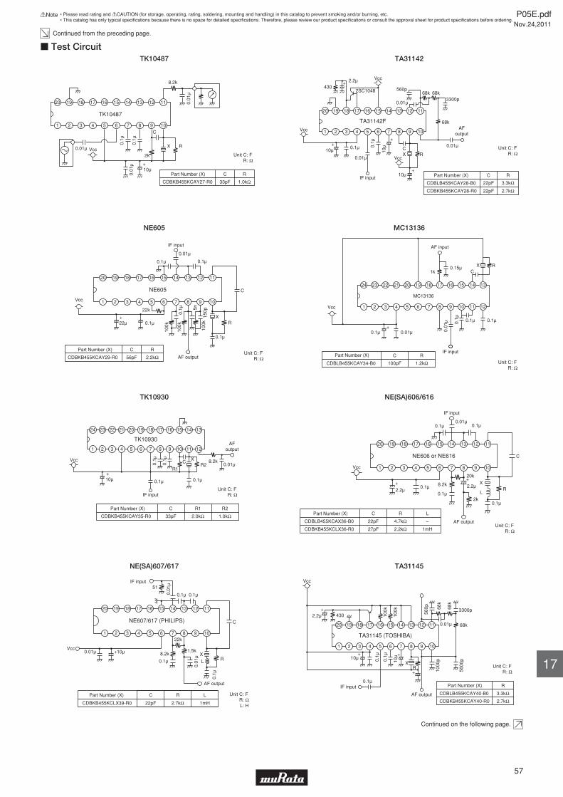
Continued from the preceding page.
20 19 18 17 16 15 14 13 12
1
R
C
2kVcc
TK10487
0.01μ
10μ+
0.1μ
0.1μ
0.01
μ
0.01
μ
8.2k
2 3 4 5 6 7 8 9
11
10
X
CDBKB455KCAY27-R0
Part Number (X) C R
33pF 1.0kΩ
: F: Ω
Unit CR
c Test CircuitTK10487
20
AFoutput
Vcc
111213141516171819
1 1098765432
430+ 2.2μ Vcc
560p68k 68k
3300p
68k
0.01μ
R
10μIF input
0.01μ
0.1μ
10μ
+
+
+10μ
0.1μ
2SC1048
0.01μ
TA31142F
XC
Vcc
CDBLB455KCAY28-B0
CDBKB455KCAY28-R0
Part Number (X) C R
22pF
22pF
3.3kΩ
2.7kΩ
: F: Ω
Unit CR
TA31142
20
AF output
Vcc
+
0.1μ
0.01μ
C
0.1μ
RX
0.1μ
150p5n
0.1μ
100k
100k
22k
0.1μ22μ
NE605
111213141516171819
1 1098765432
IF input
100k
CDBKB455KCAY29-R0
Part Number (X) C R
56pF 2.2kΩUnit C
R: F: Ω
NE605
24
1
23
2
22
3
21
4
20
5
19
6
18
7
17
8
16
9
15
10
14
11
13
12
RXC
Vcc
MC13136
0.01
μ
0.01μ
0.15μ1k
0.1μ
IF input
AF input
0.1μ 0.1μ0.1μ
+
CDBLB455KCAY34-B0
Part Number (X) C R
100pF 1.2kΩ Unit CR
: F: Ω
MC13136
24
1
23
2
22
3
21
4
20
5
19
6
18
7
17
8
16
9
15
10
14
11
13
12
R2R1
C XVcc
AFoutput
IF input
TK10930
0.01μ
0.1μ0.1μ10μ+
0.1μ
0.1μ 8.2k
CDBKB455KCAY35-R0
Part Number (X) R1 R2
2.0kΩ 1.0kΩ
C
33pF
: F: Ω
Unit CR
TK10930
20
1
19
2
18
3
17
4
16
5
15
6
14
7
13
8
12
9
11
10
RX
L
IF input
AF output
C
20k
2k
8.2k
Vcc
NE606 or NE616
0.1μ
0.1μ0.1μ
0.01μ0.1μ 0.1μ
2.2μ
+
2.2μ
+
CDBLB455KCAX36-B0
CDBKB455KCLX36-R0
Part Number (X) C R
22pF
27pF
4.7kΩ
2.2kΩ
L
–
1mH: F: Ω
Unit CR
NE(SA)606/616
20
AF output
Vcc
0.1μ
0.01
μ
0.01μ
C
RX
L
0.1μ
0.01
μ
51IF input
1119 18 17 16 15 14 13 12
1 102 3 4 5 6 7 8 922k
1.5k
NE607/617 (PHILIPS)
8.2k+10μ
0.1μ 0.1μ
CDBKB455KCLX39-R0
Part Number (X) C R
22pF 2.7kΩ
L
1mH
: F: Ω: H
Unit CRL
NE(SA)607/617
AF output
0.1μ
RX
0.1μ
1000
p
100k
10μ
IF input
3300p
Vcc
0.1μ
20
+ +
10μ
5600
p
100k+
2.2μ 430
+
0.01μ 68k
68k
68k
560p
TA31145 (TOSHIBA)
1119 18 17 16 15 14 13 12
1 102 3 4 5 6 7 8 9
CDBLB455KCAY40-B0
CDBKB455KCAY40-R0
Part Number (X) R
3.3kΩ
2.7kΩ
: F: Ω
Unit CR
TA31145
Continued on the following page.
P05E.pdfNov.24,2011
57
!Note • Please read rating and !CAUTION (for storage, operating, rating, soldering, mounting and handling) in this catalog to prevent smoking and/or burning, etc.• This catalog has only typical specifi cations because there is no space for detailed specifi cations. Therefore, please review our product specifi cations or consult the approval sheet for product specifi cations before ordering.
17
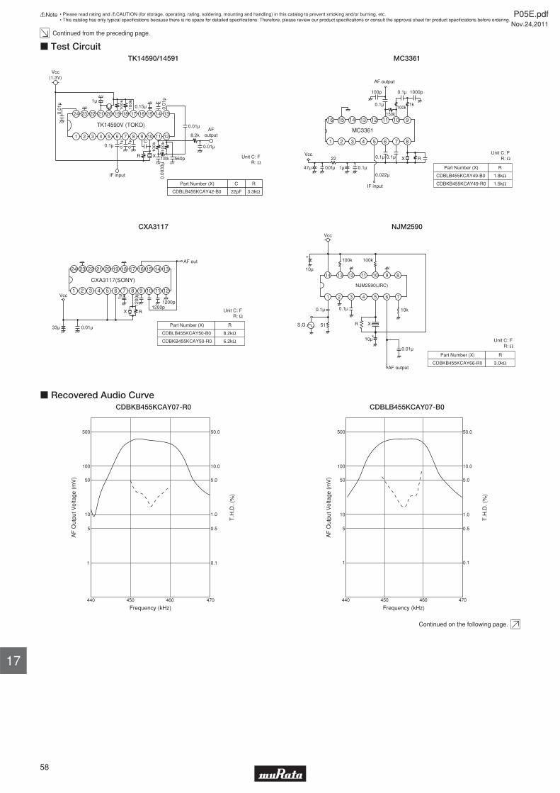
Continued from the preceding page.
AFoutput
Vcc(1.3V)
0.1μ
0.01μ
C
R0.
0033
μ1
00
k
X
IF input
24 1314151617181920212223
1 12111098765432
10
0k
8.2k
0.01μ
560p100k
0.1
μ
0.1
μ
0.01
μ 1μ
TK14590V (TOKO)
0.01
μ
0.15μ10
0k
10
0k
CDBLB455KCAY42-B0 3.3kΩ
Part Number (X) C R
22pF
: F: Ω
Unit CR
c Test CircuitTK14590/14591
47μ 0.01μ 0.1μ
Vcc
16 15 14 13 12 11 10 9
1 2 3 4 5 6 7
1μ
22
MC3361
100p 1000p
0.1μ
0.1μ
150k100k
AF output
1k
RX
IF input
0.022μ
0.1μ 0.1μ
8
Part Number (X)
CDBLB455KCAY49-B0
CDBKB455KCAY49-R0
R
1.8kΩ
1.5kΩ
Unit CR
: F: Ω
MC3361
24 22 20 19 16 15 14 13172123
1 3 5 6 9 10 11 128742
1200
p
1μ
33μ 0.01μ
1200p1200p
RX
AF out
Vcc
CXA3117(SONY)
18
Part Number (X)
CDBLB455KCAY50-B0
CDBKB455KCAY50-R0
R
8.2kΩ
6.2kΩ
Unit CR
: F: Ω
CXA3117
Part Number (X)
CDBKB455KCAY66-R0
R
3.0kΩ
Unit CR
: F: Ω
R X
10μ
S.G.
Vcc
0.1μ
51
0.1μ
AF output
10μ
10k
100k 100k
0.01μ
+
+
1 2 3 4 5 6 7
11121314 8910
NJM2590(JRC)
NJM2590
500
AF
Out
put V
olta
ge (
mV
)
T.H
.D. (
%)
440 450 460 470
Frequency (kHz)
50.0
100 10.0
50 5.0
10 1.0
5 0.5
1 0.1
c Recovered Audio CurveCDBKB455KCAY07-R0
500
AF
Out
put V
olta
ge (
mV
)
T.H
.D. (
%)
440 450 460 470
Frequency (kHz)
50.0
100 10.0
50 5.0
10 1.0
5 0.5
1 0.1
CDBLB455KCAY07-B0
Continued on the following page.
P05E.pdfNov.24,2011
58
!Note • Please read rating and !CAUTION (for storage, operating, rating, soldering, mounting and handling) in this catalog to prevent smoking and/or burning, etc.• This catalog has only typical specifi cations because there is no space for detailed specifi cations. Therefore, please review our product specifi cations or consult the approval sheet for product specifi cations before ordering.
17
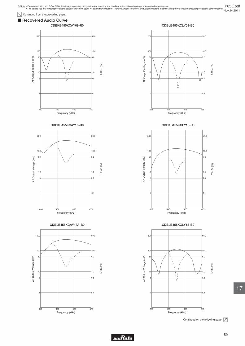
Continued from the preceding page.
500
AF
Out
put V
olta
ge (
mV
)
T.H
.D. (
%)
440 450 460 470
Frequency (kHz)
50.0
100 10.0
50 5.0
10 1.0
5 0.5
1 0.1
c Recovered Audio CurveCDBKB455KCAY09-R0
500
AF
Out
put V
olta
ge (
mV
)
T.H
.D. (
%)
395 435 475 515
Frequency (kHz)
50.0
100 10.0
50 5.0
10 1.0
5 0.5
1 0.1
CDBLB455KCLY09-B0
500
AF
Out
put V
olta
ge (
mV
)
T.H
.D. (
%)
440 450 460 470
Frequency (kHz)
50.0
100 10.0
50 5.0
10 1.0
5 0.5
1 0.1
CDBKB455KCAY13-R0
AF
Out
put V
olta
ge (
mV
)
425 445 465 485
Frequency (kHz)
500
100
50
10
5
1
T.H
.D. (
%)
50.0
10.0
5.0
1.0
0.5
0.1
CDBKB455KCLY13-R0
500
AF
Out
put V
olta
ge (
mV
)
T.H
.D. (
%)
440 450 460 470
Frequency (kHz)
50.0
100 10.0
50 5.0
10 1.0
5 0.5
1 0.1
CDBLB455KCAY13A-B0
500
AF
Out
put V
olta
ge (
mV
)
T.H
.D. (
%)
395 435 475 515
Frequency (kHz)
50.0
100 10.0
50 5.0
10 1.0
5 0.5
1 0.1
CDBLB455KCLY13-B0
Continued on the following page.
P05E.pdfNov.24,2011
59
!Note • Please read rating and !CAUTION (for storage, operating, rating, soldering, mounting and handling) in this catalog to prevent smoking and/or burning, etc.• This catalog has only typical specifi cations because there is no space for detailed specifi cations. Therefore, please review our product specifi cations or consult the approval sheet for product specifi cations before ordering.
17
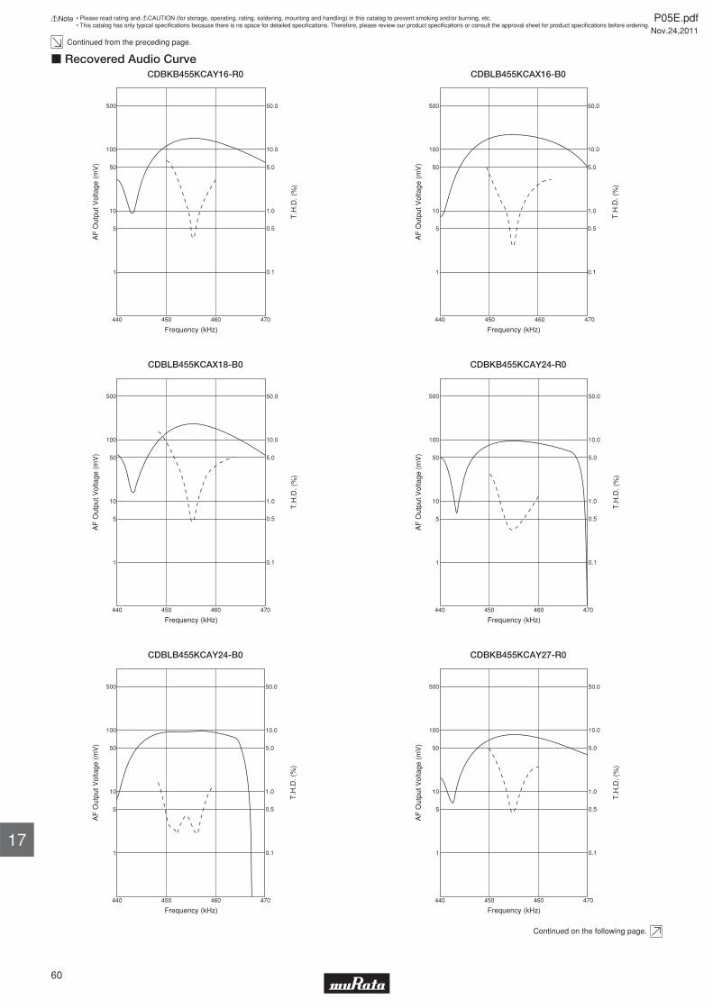
Continued from the preceding page.
AF
Out
put V
olta
ge (
mV
)
440 450 460 470
Frequency (kHz)
500
100
50
10
5
1
T.H
.D. (
%)
50.0
10.0
5.0
1.0
0.5
0.1
c Recovered Audio CurveCDBKB455KCAY16-R0
AF
Out
put V
olta
ge (
mV
)
440 450 460 470
Frequency (kHz)
500
100
50
10
5
1
T.H
.D. (
%)
50.0
10.0
5.0
1.0
0.5
0.1
CDBLB455KCAX16-B0
AF
Out
put V
olta
ge (
mV
)
440 450 460 470
Frequency (kHz)
500
100
50
10
5
1
T.H
.D. (
%)
50.0
10.0
5.0
1.0
0.5
0.1
CDBLB455KCAX18-B0
AF
Out
put V
olta
ge (
mV
)
440 450 460 470
Frequency (kHz)
500
100
50
10
5
1
T.H
.D. (
%)
50.0
10.0
5.0
1.0
0.5
0.1
CDBKB455KCAY24-R0
AF
Out
put V
olta
ge (
mV
)
440 450 460 470
Frequency (kHz)
500
100
50
10
5
1
T.H
.D. (
%)
50.0
10.0
5.0
1.0
0.5
0.1
CDBLB455KCAY24-B0
AF
Out
put V
olta
ge (
mV
)
440 450 460 470
Frequency (kHz)
500
100
50
10
5
1
T.H
.D. (
%)
50.0
10.0
5.0
1.0
0.5
0.1
CDBKB455KCAY27-R0
Continued on the following page.
P05E.pdfNov.24,2011
60
!Note • Please read rating and !CAUTION (for storage, operating, rating, soldering, mounting and handling) in this catalog to prevent smoking and/or burning, etc.• This catalog has only typical specifi cations because there is no space for detailed specifi cations. Therefore, please review our product specifi cations or consult the approval sheet for product specifi cations before ordering.
17
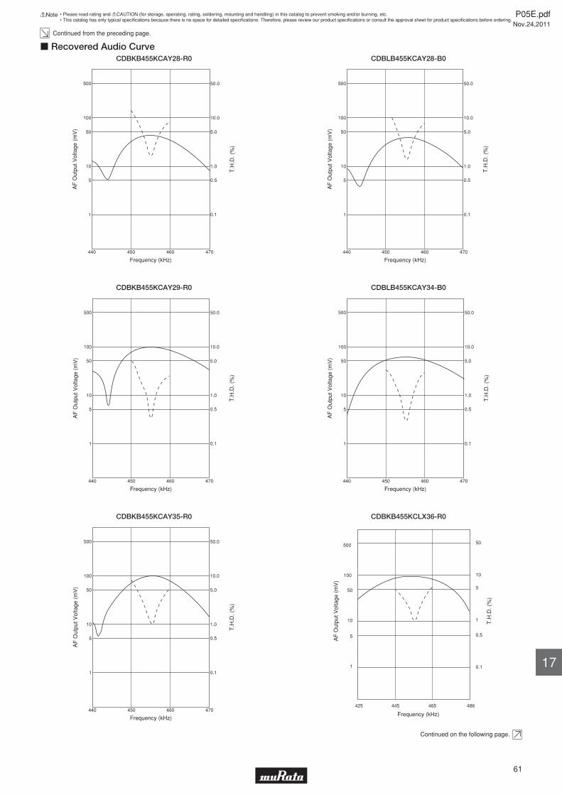
Continued from the preceding page.
AF
Out
put V
olta
ge (
mV
)
440 450 460 470
Frequency (kHz)
500
100
50
10
5
1
T.H
.D. (
%)
50.0
10.0
5.0
1.0
0.5
0.1
c Recovered Audio CurveCDBKB455KCAY28-R0
AF
Out
put V
olta
ge (
mV
)
440 450 460 470
Frequency (kHz)
500
100
50
10
5
1
T.H
.D. (
%)
50.0
10.0
5.0
1.0
0.5
0.1
CDBLB455KCAY28-B0
AF
Out
put V
olta
ge (
mV
)
440 450 460 470
Frequency (kHz)
500
100
50
10
5
1
T.H
.D. (
%)
50.0
10.0
5.0
1.0
0.5
0.1
CDBKB455KCAY29-R0
AF
Out
put V
olta
ge (
mV
)
440 450 460 470
Frequency (kHz)
500
100
50
10
5
1
T.H
.D. (
%)
50.0
10.0
5.0
1.0
0.5
0.1
CDBLB455KCAY34-B0
AF
Out
put V
olta
ge (
mV
)
440 450 460 470
Frequency (kHz)
500
100
50
10
5
1
T.H
.D. (
%)
50.0
10.0
5.0
1.0
0.5
0.1
CDBKB455KCAY35-R0
AF
Out
put V
olta
ge (
mV
)
T.H
.D. (
%)
Frequency (kHz)
1
10
100
500
425 445 465 486
0.1
0.5
5
50
5
50
1
10
CDBKB455KCLX36-R0
Continued on the following page.
P05E.pdfNov.24,2011
61
!Note • Please read rating and !CAUTION (for storage, operating, rating, soldering, mounting and handling) in this catalog to prevent smoking and/or burning, etc.• This catalog has only typical specifi cations because there is no space for detailed specifi cations. Therefore, please review our product specifi cations or consult the approval sheet for product specifi cations before ordering.
17
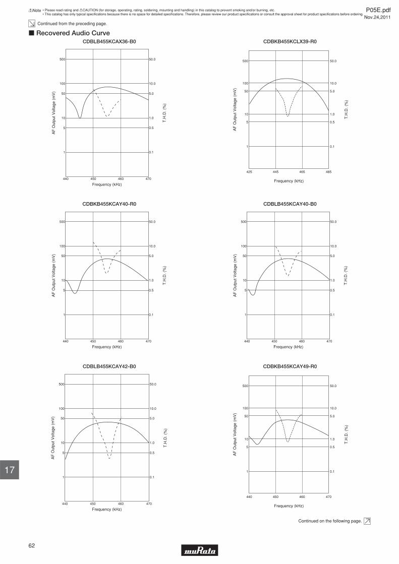
Continued from the preceding page.
AF
Out
put V
olta
ge (
mV
)
440 450 460 470
Frequency (kHz)
500
100
50
10
5
1
T.H
.D. (
%)
50.0
10.0
5.0
1.0
0.5
0.1
c Recovered Audio CurveCDBLB455KCAX36-B0
Frequency (kHz)
425 445 465 485
500
100
50
10
5
1
50.0
10.0
5.0
1.0
0.5
0.1
AF
Out
put V
olta
ge (
mV
)
T.H
.D. (
%)
CDBKB455KCLX39-R0
500
AF
Out
put V
olta
ge (
mV
)
T.H
.D. (
%)
440 450 460 470
Frequency (kHz)
50.0
100 10.0
50 5.0
10 1.0
5 0.5
1 0.1
CDBKB455KCAY40-R0
500
AF
Out
put V
olta
ge (
mV
)
T.H
.D. (
%)
440 450 460 470
Frequency (kHz)
50.0
100 10.0
50 5.0
10 1.0
5 0.5
1 0.1
CDBLB455KCAY40-B0
500
AF
Out
put V
olta
ge (
mV
)
T.H
.D. (
%)
440 450 460 470
Frequency (kHz)
50.0
100 10.0
50 5.0
10 1.0
5 0.5
1 0.1
CDBLB455KCAY42-B0
Frequency (kHz)
AF
Out
put V
olta
ge (
mV
)
T.H
.D. (
%)
440 450 460 470
500
100
50
10
5
1
50.0
10.0
5.0
1.0
0.5
0.1
CDBKB455KCAY49-R0
Continued on the following page.
P05E.pdfNov.24,2011
62
!Note • Please read rating and !CAUTION (for storage, operating, rating, soldering, mounting and handling) in this catalog to prevent smoking and/or burning, etc.• This catalog has only typical specifi cations because there is no space for detailed specifi cations. Therefore, please review our product specifi cations or consult the approval sheet for product specifi cations before ordering.
17
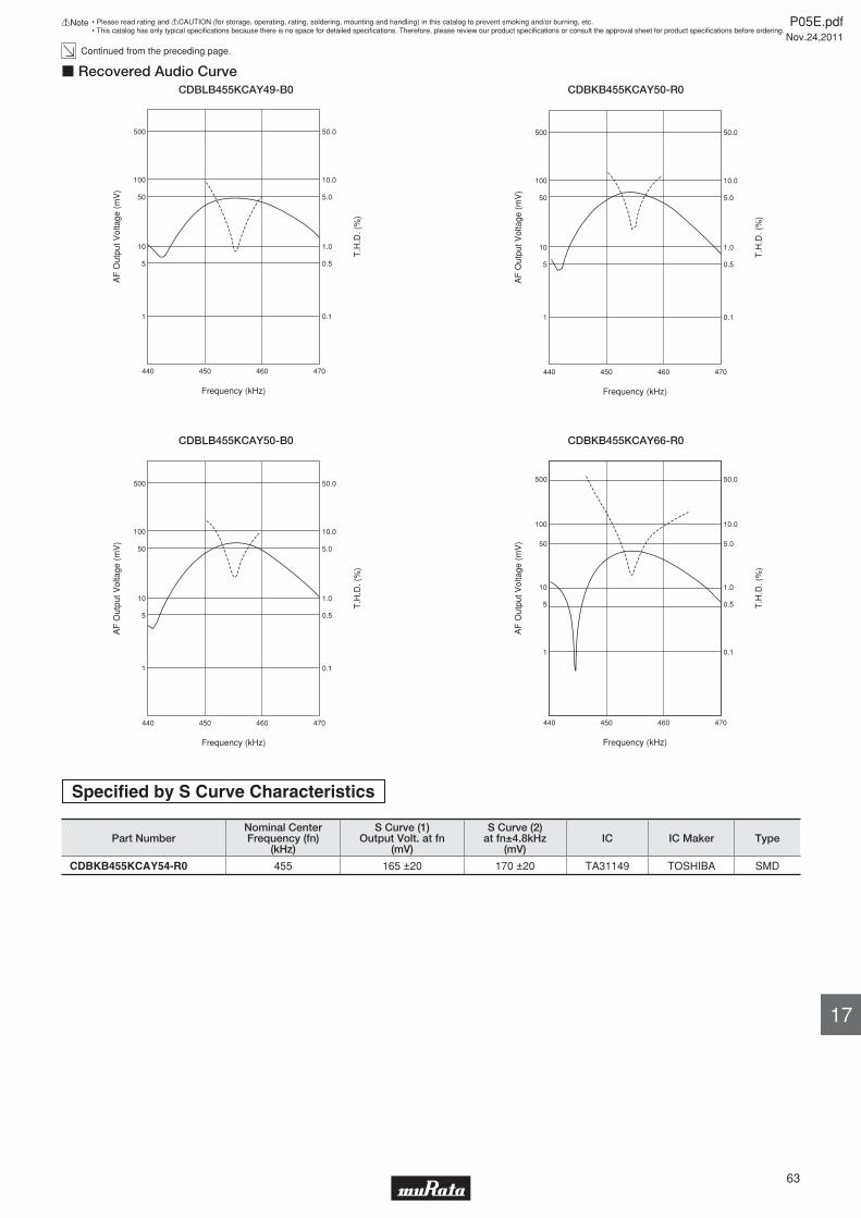
Continued from the preceding page.
Frequency (kHz)
AF
Out
put V
olta
ge (
mV
)
T.H
.D. (
%)
440 450 460 470
500
100
50
10
5
1
50.0
10.0
5.0
1.0
0.5
0.1
c Recovered Audio CurveCDBLB455KCAY49-B0
Frequency (kHz)
AF
Out
put V
olta
ge (
mV
)
T.H
.D. (
%)
440 450 460 470
500
100
50
10
5
1
50.0
10.0
5.0
1.0
0.5
0.1
CDBKB455KCAY50-R0
Frequency (kHz)
AF
Out
put V
olta
ge (
mV
)
T.H
.D. (
%)
440 450 460 470
500
100
50
10
5
1
50.0
10.0
5.0
1.0
0.5
0.1
CDBLB455KCAY50-B0
Frequency (kHz)
AF
Out
put V
olta
ge (
mV
)
T.H
.D. (
%)
440 450 460 470
500
100
50
10
5
1
50.0
10.0
5.0
1.0
0.5
0.1
CDBKB455KCAY66-R0
Specifi ed by S Curve Characteristics
Part NumberNominal CenterFrequency (fn)
(kHz)
S Curve (1)Output Volt. at fn
(mV)
S Curve (2)at fn±4.8kHz
(mV)IC IC Maker Type
CDBKB455KCAY54-R0 455 165 ±20 170 ±20 TA31149 TOSHIBA SMD
P05E.pdfNov.24,2011
63
!Note • Please read rating and !CAUTION (for storage, operating, rating, soldering, mounting and handling) in this catalog to prevent smoking and/or burning, etc.• This catalog has only typical specifi cations because there is no space for detailed specifi cations. Therefore, please review our product specifi cations or consult the approval sheet for product specifi cations before ordering.
17
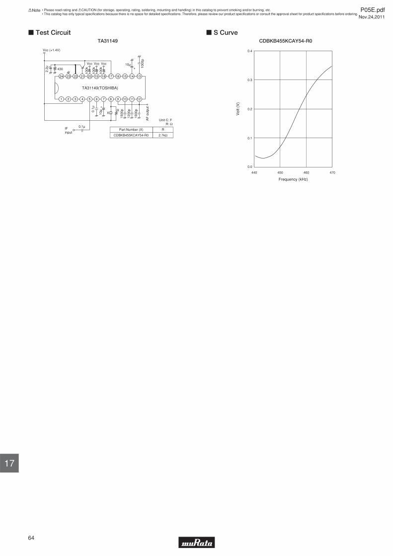
24 22 16 15
1 3 5 9742
1000
p
10μ0.
1μ
10μ
1000
p
100k
0.1μ
RX
AF
out
put
1200
p
1500
p
Vcc (+1.4V)
TA31149(TOSHIBA)
12118 106
IFinput
17
2.2μ 430
23 21 20
Vcc
100k
Vcc
100k
Vcc
19 18 14 13
++
+
Part Number (X)
CDBKB455KCAY54-R0
R
2.7kΩ
Unit CR
: F: Ω
c Test CircuitTA31149
440 450 460 470
0.0
0.1
0.2
0.3
0.4
Frequency (kHz)
Vol
t (V
)
c S CurveCDBKB455KCAY54-R0
P05E.pdfNov.24,2011
64
!Note • Please read rating and !CAUTION (for storage, operating, rating, soldering, mounting and handling) in this catalog to prevent smoking and/or burning, etc.• This catalog has only typical specifi cations because there is no space for detailed specifi cations. Therefore, please review our product specifi cations or consult the approval sheet for product specifi cations before ordering.
17
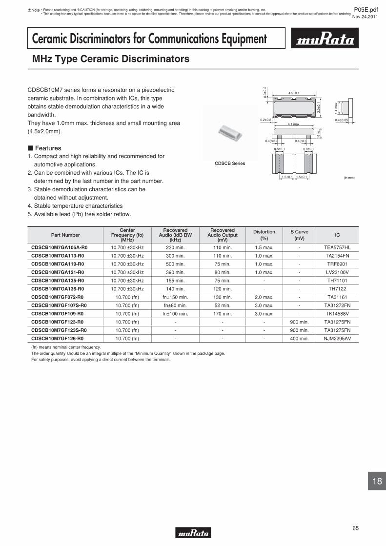
Ceramic Discriminators for Communications EquipmentMHz Type Ceramic Discriminators
CDSCB10M7 series forms a resonator on a piezoelectric ceramic substrate. In combination with ICs, this type obtains stable demodulation characteristics in a wide bandwidth.They have 1.0mm max. thickness and small mounting area(4.5x2.0mm).
c Features1. Compact and high reliability and recommended for automotive applications. 2. Can be combined with various ICs. The IC is determined by the last number in the part number.3. Stable demodulation characteristics can be obtained without adjustment.4. Stable temperature characteristics5. Available lead (Pb) free solder refl ow.
4.1 max.
1.0
max
.
4.5±0.1
0.2±0.2
2.0±
0.1
0.3±
0.2
0.4(ref.) 0.4(ref.)
1.4
max
.
0.4±0.05
1.5±0.1
0.8±0.10.8±0.1
1.5±0.1 (in mm)
CDSCB Series
Part NumberCenter
Frequency (fo)(MHz)
RecoveredAudio 3dB BW
(kHz)
RecoveredAudio Output
(mV)
Distortion(%)
S Curve(mV)
IC
CDSCB10M7GA105A-R0 10.700 ±30kHz 220 min. 110 min. 1.5 max. - TEA5757HL
CDSCB10M7GA113-R0 10.700 ±30kHz 300 min. 110 min. 1.0 max. - TA2154FN
CDSCB10M7GA119-R0 10.700 ±30kHz 500 min. 75 min. 1.0 max. - TRF6901
CDSCB10M7GA121-R0 10.700 ±30kHz 390 min. 80 min. 1.0 max. - LV23100V
CDSCB10M7GA135-R0 10.700 ±30kHz 155 min. 75 min. - - TH71101
CDSCB10M7GA136-R0 10.700 ±30kHz 140 min. 120 min. - - TH7122
CDSCB10M7GF072-R0 10.700 (fn) fn±150 min. 130 min. 2.0 max. - TA31161
CDSCB10M7GF107S-R0 10.700 (fn) fn±80 min. 52 min. 3.0 max. - TA31272FN
CDSCB10M7GF109-R0 10.700 (fn) fn±100 min. 170 min. 3.0 max. - TK14588V
CDSCB10M7GF123-R0 10.700 (fn) - - - 900 min. TA31275FN
CDSCB10M7GF123S-R0 10.700 (fn) - - - 900 min. TA31275FN
CDSCB10M7GF126-R0 10.700 (fn) - - - 400 min. NJM2295AV
(fn) means nominal center frequency.
The order quantity should be an integral multiple of the "Minimum Quantity" shown in the package page.
For safety purposes, avoid applying a direct current between the terminals.
P05E.pdfNov.24,2011
65
!Note • Please read rating and !CAUTION (for storage, operating, rating, soldering, mounting and handling) in this catalog to prevent smoking and/or burning, etc.• This catalog has only typical specifi cations because there is no space for detailed specifi cations. Therefore, please review our product specifi cations or consult the approval sheet for product specifi cations before ordering.
18
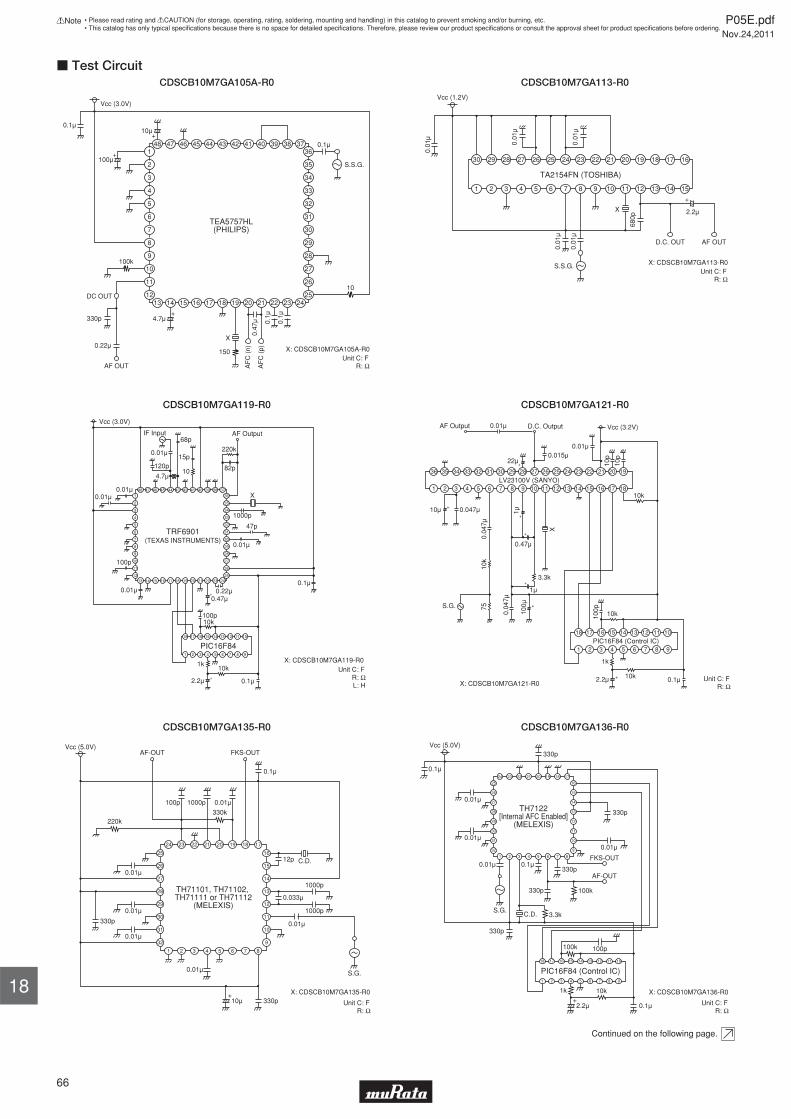
48 41424344454647
1312
20191817161514
4.7μ
X
150
S.S.G.
Vcc (3.0V)
0.1μ
0.47
μ
TEA5757HL(PHILIPS)
+
40
21
39
22
38
23
37
24
X: CDSCB10M7GA105A-R0
0.1μ
0.1μ10μ
100μ
10
100k
+
+
AF
C (
n)
AF
C (
p)
AF OUT
DC OUT
330p
0.22μ
11
10
9
8
7
6
5
4
3
2
1
25
26
27
28
29
30
31
32
33
34
35
36
0.1μ
Unit CR
: F: Ω
c Test CircuitCDSCB10M7GA105A-R0
30 23242526272829
1 8765432
2.2μ
D.C. OUT
S.S.G.
Vcc (1.2V)
AF OUT
0.01
μ
0.01
μ
0.01
μ
0.01
μ
680p
TA2154FN (TOSHIBA)
+
22
9
21
10
20
11
19
12
18
13
17
14
16
15
X: CDSCB10M7GA113-R0
0.01
μ
X
Unit CR
: F: Ω
CDSCB10M7GA113-R0
0.01μ
0.01μ
0.01μ0.01μ
0.01μ0.47μ
2.2μ 0.1μ
0.1μ0.22μ
4.7μ
120p
220k
68p
15p
82p
47p
1000p
100p
100p10k
10k1k
+
10
IF Input AF Output
Vcc (3.0V)
(TEXAS INSTRUMENTS)TRF6901
PIC16F84
X
Unit CRL
: F: Ω: H
+
X: CDSCB10M7GA119-R0
1
2
3
4
5
6
7
8
9
10
11
12
36
35
34
33
32
31
30
29
28
27
26
2513 14 15 16 17 18 19 20 21 22 23 24
48 47 46 45 44 43 42 41 40 39 38 37
18 17 16 15 14 13 12 11 10
1 2 3 4 5 6 7 8 9
CDSCB10M7GA119-R0
0.47μ
0.01μAF Output D.C. Output
LV23100V (SANYO)
PIC16F84 (Control IC)
10k
10k
10k
Vcc (3.2V)
1μ0.047μ0.
047μ
2.2μ 0.1μ
1k
0.04
7μ10
k75
0.015μ0.01μ
100μ
10p
100p
10p
22μ
10μ
3.3k
+
1μ+
+
+
+
+
+
S.G.
X
Unit CR
: F: ΩX: CDSCB10M7GA121-R0
36 35 34 33 32 31 30 2829 27 26 25 24 23 22 21 20 19
1 2 3 4 5 6 7 98 10 11 12 13 14 15 16 17 18
18
1
17
2
16
3
15
4
14
5
13
6
12
7
10
9
11
8
CDSCB10M7GA121-R0
Unit CR
: F: Ω
X: CDSCB10M7GA135-R0
1 2 3 4 5 6 7 8
9
10
11
12
13
14
15
16
1718192021222324
25
26
27
28
29
30
31
32
220k
0.01μ
0.01μ
1000p
0.1μ
0.01μ1000p100p
330p
0.033μ
12p
0.01μ
0.01μ
0.01μ
1000p
C.D.
330p10μ+
S.G.
Vcc (5.0V)
TH71101, TH71102, TH71111 or TH71112
(MELEXIS)
FKS-OUTAF-OUT
330k
CDSCB10M7GA135-R0
1 2 3 4 5 6 7 8
1 2 3 4 5 6 7 8 9
18 17 16 15 14 13 12 11 10
9
10
11
12
13
14
15
16
1718192021222324
25
26
27
28
29
30
31
32
Unit CR
: F: Ω
X: CDSCB10M7GA136-R0
0.1μ
2.2μ
1k
100k
3.3k
+0.1μ
100p
10k
PIC16F84 (Control IC)
TH7122[Internal AFC Enabled]
(MELEXIS)
Vcc (5.0V)
0.01μ
0.01μ
0.1μ0.01μ330p
330p 100k
330p
S.G.C.D.
FKS-OUT
AF-OUT
330p
330p
0.01μ
CDSCB10M7GA136-R0
Continued on the following page.
P05E.pdfNov.24,2011
66
!Note • Please read rating and !CAUTION (for storage, operating, rating, soldering, mounting and handling) in this catalog to prevent smoking and/or burning, etc.• This catalog has only typical specifi cations because there is no space for detailed specifi cations. Therefore, please review our product specifi cations or consult the approval sheet for product specifi cations before ordering.
18
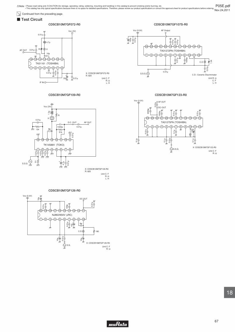
Continued from the preceding page.
16
Vcc (3V)
9101112131415
1 8765432
IF IN
AF OUT
0.01μ
33μ 0.01μ
R
10p
4.7μ
X0.01μ
0.01μ
0.01
μ
+
TA31161 (TOSHIBA)
X: CDSCB10M7GF072-R0R: 820
Unit CRL
: F: Ω: H
c Test CircuitCDSCB10M7GF072-R0
Vcc (5.0V)
+
1 2 3 4 5 6 7 8 9 10 11 12
24 23 22 21 20 19 18 17 16 15 14 13
0.01μ
TA31272FN (TOSHIBA)
AF Output
C.D.
0.01
μ
0.01
μ
1000
p
100μ
0.01
μ
0.01
μ
0.01
μ
1.2k
C.D.: Ceramic Discriminator
Unit RCL
: Ω: F: H
S.S.G.
CDSCB10M7GF107S-R0
0.01μ
0.01μ
Vcc (3V)
12k51k
1000p8p
+S.S.G.
R
D.C. OUT AF OUT
X
0.01
μ
0.01
μ
0.01
μ
0.01
μ
4.7μ51
0.01
μ
1.2μ
TK14588V (TOKO)
Unit CRL
: F: Ω: H
X: CDSCB10M7GF109-R0R: 820
910111213141516
87654321
CDSCB10M7GF109-R0
Vcc (5.0V)
1 2 3 4 5 6 7 8 9 10 11 12
24 23 22 21 20 19 18 17 16 15 14 13
0.1μ
0.01
μ
TA31275FN (TOSHIBA)
1000
p
3300
p
0.01
μ AF OUT
DC-OUT
0.01
μ
0.01
μ
0.1μ
0.1μ
0.1μ
1.8k
0.01
μ
X: CDSCB10M7GF123-R0
Unit CR
: F: Ω
S.S.G.
CDSCB10M7GF123-R0
Vcc (5.0V)
1 2 3 4 5 6 7 8 9 10
20 19 18 17 16 15 14 13 12 11
NJM2295AV (JRC)
0.01
μ
DC-OUT
100p
0.01
μ
10μ
0.01
μ
10μ
180
8p
C.D.
0.01
μ
X: CDSCB10M7GF126-R0
Unit CR
: F: Ω
S.G.
+
+
10μ
+
10μ
+
CDSCB10M7GF126-R0
P05E.pdfNov.24,2011
67
!Note • Please read rating and !CAUTION (for storage, operating, rating, soldering, mounting and handling) in this catalog to prevent smoking and/or burning, etc.• This catalog has only typical specifi cations because there is no space for detailed specifi cations. Therefore, please review our product specifi cations or consult the approval sheet for product specifi cations before ordering.
18
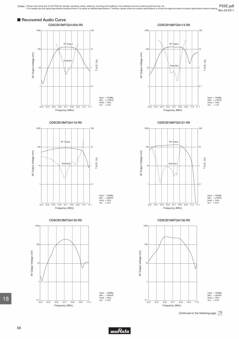
AF
Out
put V
olta
ge (
mV
)
T.H
.D. (
%)
Frequency (MHz)
Inputfdev.fmod.Vcc
= 100dBμ= ±75kHz= 1kHz= 3.0V
1
10
100
1000
10.3 10.4 10.5 10.6 10.7 10.8 10.9 11.0 11.1
0.1
1
10
100
AF Output
Distortion
c Recovered Audio CurveCDSCB10M7GA105A-R0
AF
Out
put V
olta
ge (
mV
)
T.H
.D. (
%)
Frequency (MHz)
Inputfdev.fmod.Vcc
= 100dBμ= ±75kHz= 1kHz= 1.2V
1
10
100
1000
10.3 10.4 10.5 10.6 10.7 10.8 10.9 11.0 11.1
0.1
1
10
100
AF Output
Distortion
CDSCB10M7GA113-R0
AF
Out
put V
olta
ge (
mV
)
T.H
.D. (
%)
Frequency (MHz)
Inputfdev.fmod.Vcc
= 100dBμ= ±60kHz= 1kHz= 3.0V
1
10
100
1000
10.3 10.4 10.5 10.6 10.7 10.8 10.9 11.0 11.1
0.1
1
10
100
AF Output
Distortion
CDSCB10M7GA119-R0
AF
Out
put V
olta
ge (
mV
)
T.H
.D. (
%)
Frequency (MHz)
Inputfdev.fmod.Vcc
= 100dBμ= ±75kHz= 1kHz= 3.2V
1
10
100
1000
10.3 10.4 10.5 10.6 10.7 10.8 10.9 11.0 11.1
0.1
1
10
100
AF Output
Distortion
CDSCB10M7GA121-R0
AF
Out
put V
olta
ge (
mV
)
Frequency (MHz)
Inputfdev.fmod.Vcc
= 100dBμ= ±50kHz= 1kHz= 5.0V
1
10
100
1000
10.4 10.5 10.6 10.7 10.8 10.9 11.00.1
CDSCB10M7GA135-R0
AF
Out
put V
olta
ge (
mV
)
Frequency (MHz)
Inputfdev.fmod.Vcc
= 100dBμ= ±50kHz= 1kHz= 5.0V
1
10
100
1000
10.4 10.5 10.6 10.7 10.8 10.9 11.00.1
CDSCB10M7GA136-R0
Continued on the following page.
P05E.pdfNov.24,2011
68
!Note • Please read rating and !CAUTION (for storage, operating, rating, soldering, mounting and handling) in this catalog to prevent smoking and/or burning, etc.• This catalog has only typical specifi cations because there is no space for detailed specifi cations. Therefore, please review our product specifi cations or consult the approval sheet for product specifi cations before ordering.
18
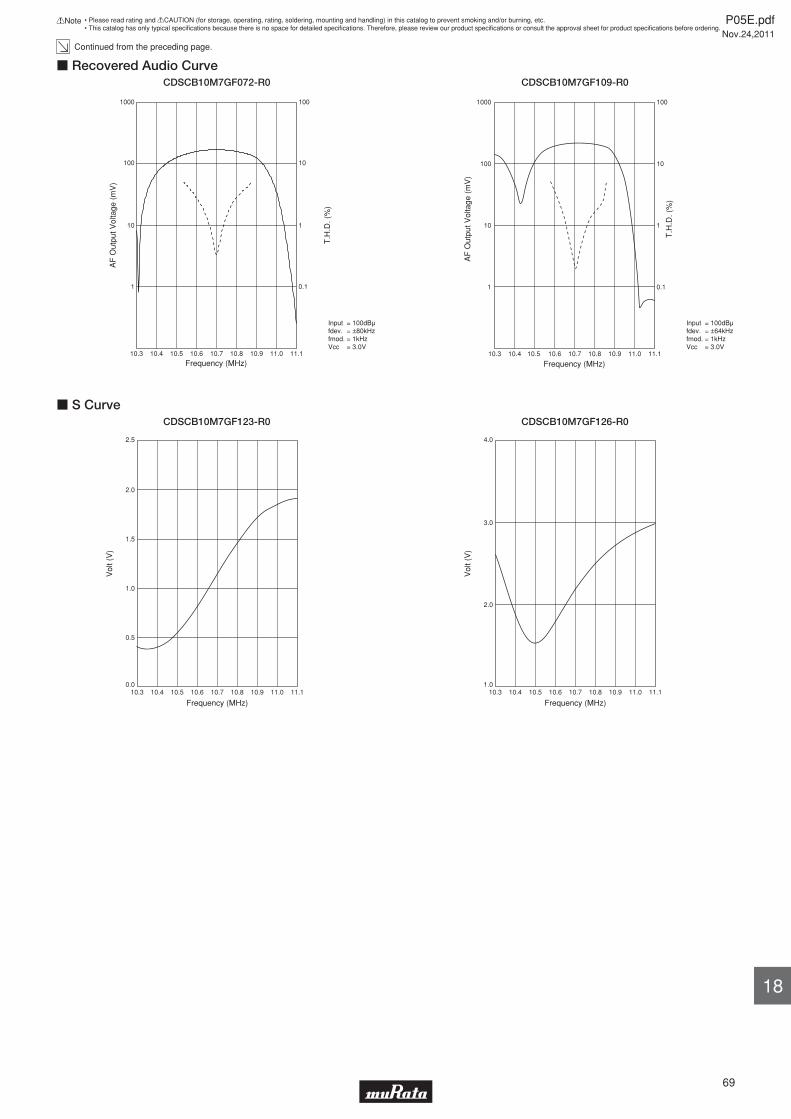
Continued from the preceding page.
AF
Out
put V
olta
ge (
mV
)
T.H
.D. (
%)
Frequency (MHz)
100 10
1000 100
10 1
1 0.1
10.3 10.5 10.7 10.9 11.110.4 10.6 10.8 11.0
Inputfdev.fmod.Vcc
= 100dBμ= ±80kHz= 1kHz= 3.0V
c Recovered Audio CurveCDSCB10M7GF072-R0
Inputfdev.fmod.Vcc
= 100dBμ= ±64kHz= 1kHz= 3.0V
AF
Out
put V
olta
ge (
mV
)
T.H
.D. (
%)
Frequency (MHz)
1000
100
10
1
100
10
1
0.1
10.3 10.5 10.7 10.9 11.110.4 10.6 10.8 11.0
CDSCB10M7GF109-R0
Vol
t (V
)
Frequency (MHz)
0.5
0.0
1.0
1.5
2.0
2.5
10.3 10.4 10.5 10.6 10.7 10.8 10.9 11.0 11.1
c S CurveCDSCB10M7GF123-R0
Vol
t (V
)
Frequency (MHz)
1.0
2.0
3.0
4.0
10.3 10.4 10.5 10.6 10.7 10.8 10.9 11.0 11.1
CDSCB10M7GF126-R0
P05E.pdfNov.24,2011
69
!Note • Please read rating and !CAUTION (for storage, operating, rating, soldering, mounting and handling) in this catalog to prevent smoking and/or burning, etc.• This catalog has only typical specifi cations because there is no space for detailed specifi cations. Therefore, please review our product specifi cations or consult the approval sheet for product specifi cations before ordering.
18
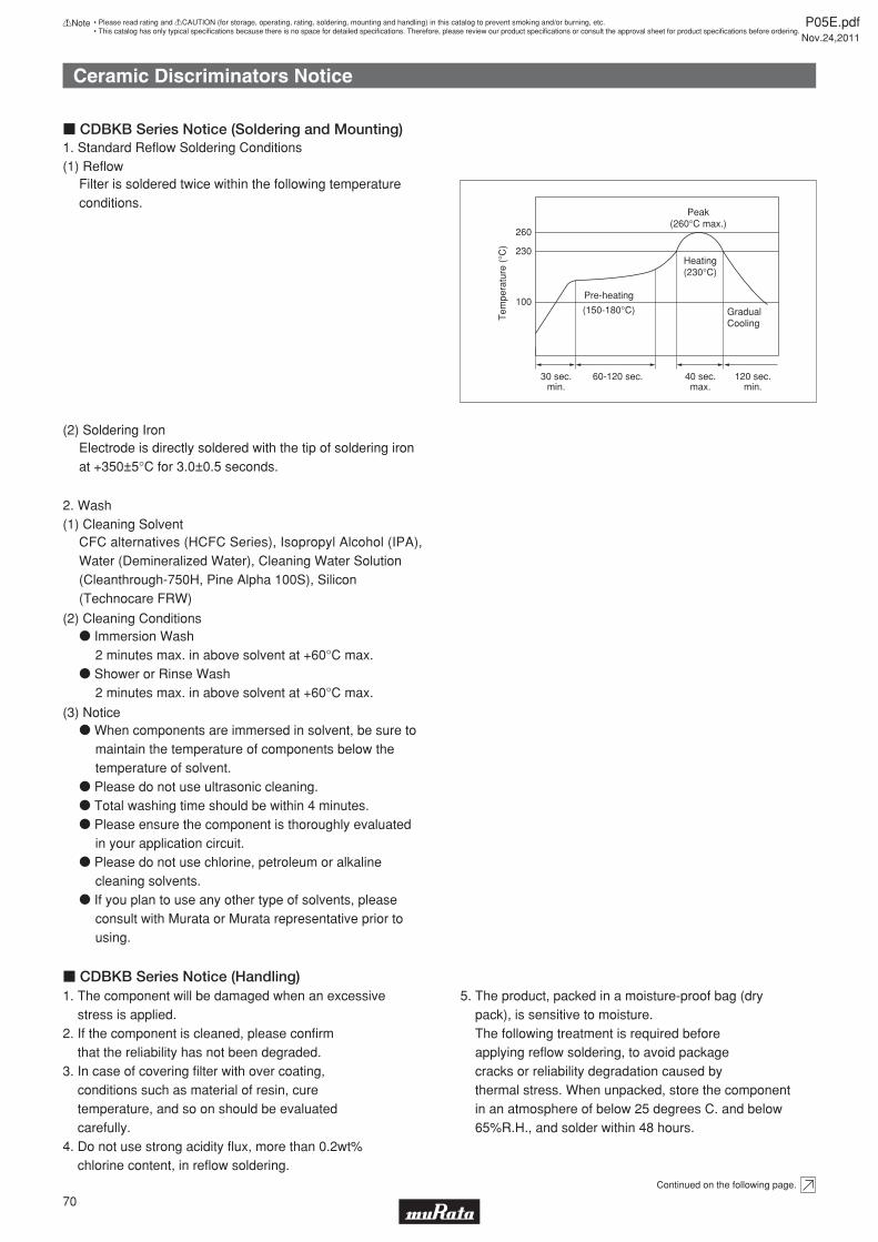
Ceramic Discriminators Notice
1. Standard Reflow Soldering Conditions (1) Reflow
CFC alternatives (HCFC Series), Isopropyl Alcohol (IPA), Water (Demineralized Water), Cleaning Water Solution (Cleanthrough-750H, Pine Alpha 100S), Silicon (Technocare FRW)
2. Wash(1) Cleaning Solvent
o Immersion Wash2 minutes max. in above solvent at +60°C max.
o Shower or Rinse Wash2 minutes max. in above solvent at +60°C max.
(2) Cleaning Conditions
o When components are immersed in solvent, be sure to maintain the temperature of components below the temperature of solvent.
o Please do not use ultrasonic cleaning.o Total washing time should be within 4 minutes.o Please ensure the component is thoroughly evaluated
in your application circuit.o Please do not use chlorine, petroleum or alkaline
cleaning solvents.o If you plan to use any other type of solvents, please
consult with Murata or Murata representative prior to using.
(3) Notice
Electrode is directly soldered with the tip of soldering iron at +350±5°C for 3.0±0.5 seconds.
(2) Soldering Iron
Peak(260°C max.)
Heating(230°C)
GradualCooling
Pre-heating
(150-180°C)100
230
260
Tem
pera
ture
(°C
)
60-120 sec. 40 sec.max.
30 sec.min.
120 sec.min.
Filter is soldered twice within the following temperature conditions.
c CDBKB Series Notice (Soldering and Mounting)
Continued on the following page.
c CDBKB Series Notice (Handling)
P05E.pdfNov.24,2011
70
!Note • Please read rating and !CAUTION (for storage, operating, rating, soldering, mounting and handling) in this catalog to prevent smoking and/or burning, etc.• This catalog has only typical specifi cations because there is no space for detailed specifi cations. Therefore, please review our product specifi cations or consult the approval sheet for product specifi cations before ordering.
1. The component will be damaged when an excessive stress is applied.2. If the component is cleaned, please confi rm that the reliability has not been degraded.3. In case of covering fi lter with over coating, conditions such as material of resin, cure temperature, and so on should be evaluated carefully.4. Do not use strong acidity fl ux, more than 0.2wt% chlorine content, in refl ow soldering.
5. The product, packed in a moisture-proof bag (dry pack), is sensitive to moisture. The following treatment is required before applying refl ow soldering, to avoid package cracks or reliability degradation caused by thermal stress. When unpacked, store the component in an atmosphere of below 25 degrees C. and below 65%R.H., and solder within 48 hours.
Ceramic Discriminators Notice
c CDBLB Series Notice (Handling)
Continued from the preceding page.
P05E.pdfNov.24,2011
71
!Note • Please read rating and !CAUTION (for storage, operating, rating, soldering, mounting and handling) in this catalog to prevent smoking and/or burning, etc.• This catalog has only typical specifi cations because there is no space for detailed specifi cations. Therefore, please review our product specifi cations or consult the approval sheet for product specifi cations before ordering.
1. Do not use this product with bend. The component may be damaged if excess mechanical stress is applied to it mounted on the printed circuit board.2. The component will be damaged when an excessive stress is applied.3. No type of refl ow soldering should be applied to this component.4. Do not clean or wash the component as it is not hermetically sealed.
5. Do not use strong acidity fl ux, more than 0.2wt% chlorine content, in fl ow soldering. 6. In case of covering discriminator with over coating, conditions such as material of resin, cure temperature, and so on should be evaluated carefully.
Ceramic Discriminators Notice
Continued on the following page.
Filter is soldered twice within the following temperature conditions.
1. Standard Reflow Soldering Conditions(1) Reflow
Filter is soldered at +300±5°C for 3.0±0.5 seconds. The soldering iron should not touch the filter while soldering.
(2) Soldering Iron
The component is recommended with placement machines that employ optical placement capabilities. The component might be damaged by excessive mechanical force. Please make sure that you have evaluated by using placement machines before going into mass production. Do not use placement machines that utilize mechanical positioning. Please contact Murata for details beforehand.
(3) Condition for Placement Machines
(a) The component may be damaged if excess mechanical stress is applied to it mounted on the printed circuit board.
(b) Design layout of components on the PC board to minimize the stress imposed on the warp or flexure of the board.
(c) After installing components, if solder is excessively applied to the circuit board, mechanical stress will cause destruction resistance characteristics to degrade. To prevent this, be extremely careful in determining shape and dimension before designing the circuit board diagram.
(d) When the positioning claws and pick-up nozzle are worn, the load is applied to the components while positioning is concentrated on positioning accuracy, etc. Careful checking and maintenance are necessary to prevent unexpected trouble.
(e) When correcting components with a soldering iron, the tip of the soldering iron should not directly touch the component. Depending on the soldering conditions, the effective area of terminations may be reduced. Solder containing Ag should be used to prevent the electrode erosion.
(4) Other
o Soldering and Mounting
Tem
pera
ture
(°C
)
100
230
260
30 sec.min.
40 sec.max.
Peak(260°C max.)
Pre-heating(150-180°C)
Heating(230°C)
GradualCooling
120 sec.min.
60-120 sec.
[Component Direction]
[Component Layout Close to Board]
Place the component laterally to the direction in which stress acts.
Susceptibility to stress is in the order of : A>C>B
B
A CSlit
Perforation
c CDSCB Series Notice
P05E.pdfNov.24,2011
72
!Note • Please read rating and !CAUTION (for storage, operating, rating, soldering, mounting and handling) in this catalog to prevent smoking and/or burning, etc.• This catalog has only typical specifi cations because there is no space for detailed specifi cations. Therefore, please review our product specifi cations or consult the approval sheet for product specifi cations before ordering.
Ceramic Discriminators Notice
o Storage and Operating Conditions
o RatingThe component may be damaged if excessive mechanical stress is applied.
o Handling1. Accurate test circuit values are required to measure
electrical characteristics. Miscorrelation may be caused if there is any deviation, especially stray capacitance, from the test circuit in the specification.
2. For safety purposes, avoid applying a direct current between the terminals.
1. Product Storage ConditionPlease store the products in a room where the temperature/humidity is stable, and avoid places where there are large temperature changes. Please store the products under the following conditions: Temperature: -10 to +40°CHumidity: 15 to 85% R.H.
2. Expiration Date on StorageExpiration date (shelf life) of the products is six months after delivery under the conditions of a sealed and unopened package. Please use the products within six months after delivery. If you store the products for a long time (more than six months), use carefully because solderability may be degraded due to storage under poor conditions.Please confirm solderability and characteristics for the products regularly.
3. Notice on Product Storage(1) Please do not store the products in a chemical
atmosphere (Acids, Alkali, Bases, Organic gas, Sulfides and so on), because the characteristics may be reduced in quality and may be degraded in solderability due to storage in a chemical atmosphere.
(2) Please do not put the products directly on the floor without anything under them to avoid damp places and/or dusty places.
(3) Please do not store the products in places such as a damp heated place or any place exposed to direct sunlight or excessive vibration.
(4) Please use the products immediately after the package is opened, because the characteristics may be reduced in quality and/or be degraded in solderability due to storage under poor condition.
(5) Please do not drop the products to avoid cracking of ceramic element.
4. OtherPlease be sure to consult with our sales representative or engineer whenever the products are to be used in conditions not listed above.
Continued from the preceding page.
Do not clean or wash the component as it is not hermetically sealed.
2. Wash
In case of overcoating the component, conditions such as material of resin, cure temperature, and so on should be evaluated well.
3. Coating
P05E.pdfNov.24,2011
73
!Note • Please read rating and !CAUTION (for storage, operating, rating, soldering, mounting and handling) in this catalog to prevent smoking and/or burning, etc.• This catalog has only typical specifi cations because there is no space for detailed specifi cations. Therefore, please review our product specifi cations or consult the approval sheet for product specifi cations before ordering.
Ceramic Discriminators Standard Land Pattern Dimensions/Packaging
(in mm)
1.2 1.2
2.0
4.9
2.6
c Standard Land Pattern DimensionsCDBKB Series
2.6
1.0 2.0 1.0
3.0
(in mm)
CDSCB Series
Part Number Taping ø180mm Bulk
500
2000
500
CDBKB Series
CDBLB Series
CDSCB Series
(pcs.)The order quantity should be an integral multiple of the "Minimum Quantity" shown above.
c Minimum Quantity
User direction of feed
Cover film3° max.
+0.1-0.0
+1.
0-0
+0
-3.0
Dimensions of Carrier Tape Dimensions of Reel
(in mm)
LeaderCover film
Empty EmptyComponents
Trailer160 to 190
160 to 200
400 to 560
(ø60
)
(ø18
0
)
17.0±0.3
4.0±0.1
7.5±
0.1
1.75
±0.
1
16.0
±0.
15
3.3±0.1
7.2±
0.1
8.0±0.1
6.3±0.1
2.0±0.1
19.4±1.0
ø13.0±0.5
ø1.5
2.0±0.2
c CDBKB Series
Continued on the following page.
P05E.pdfNov.24,2011
74
!Note • Please read rating and !CAUTION (for storage, operating, rating, soldering, mounting and handling) in this catalog to prevent smoking and/or burning, etc.• This catalog has only typical specifi cations because there is no space for detailed specifi cations. Therefore, please review our product specifi cations or consult the approval sheet for product specifi cations before ordering.
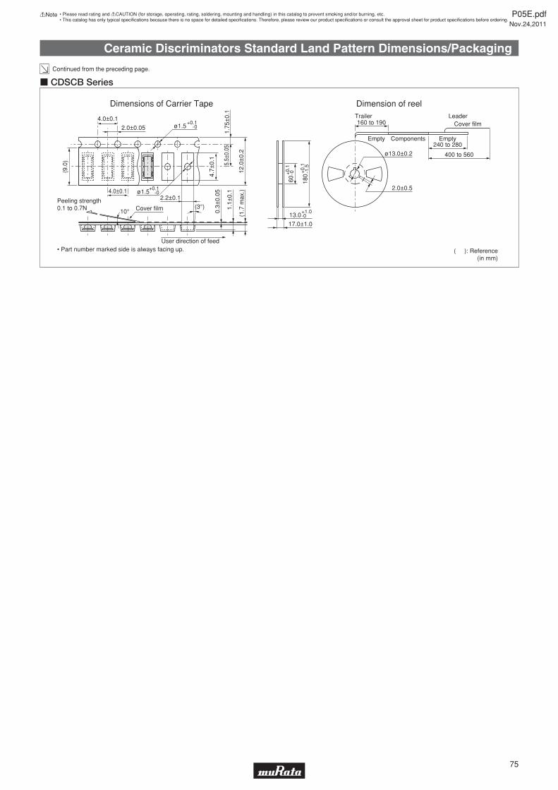
Ceramic Discriminators Standard Land Pattern Dimensions/Packaging
Continued from the preceding page.
4.0±0.1
Cover film
4.0±0.1
2.0±0.05
12.0
±0.
2
(9.0
)
ø1.5+0.1
-0
ø1.5+0.1
-0
5.5±
0.05
1.75
±0.
1
4.7±
0.1
User direction of feed
0.3±
0.05
1.1±
0.1
(3°)
2.2±0.1
0.1 to 0.7N 10°
Dimension of reel
( ): Reference(in mm)
ø13.0±0.2
2.0±0.5
17.0±1.0
180
+0.
1-1
.5
60+
0.1
-0
240 to 280
400 to 560
160 to 190 Cover film
13.0+1.0-0
c CDSCB Series
P05E.pdfNov.24,2011
75
!Note • Please read rating and !CAUTION (for storage, operating, rating, soldering, mounting and handling) in this catalog to prevent smoking and/or burning, etc.• This catalog has only typical specifi cations because there is no space for detailed specifi cations. Therefore, please review our product specifi cations or consult the approval sheet for product specifi cations before ordering.
!Note P05E.pdfNov.24,2011
• Please read rating and !CAUTION (for storage, operating, rating, soldering, mounting and handling) in this catalog to prevent smoking and/or burning, etc.• This catalog has only typical specifi cations because there is no space for detailed specifi cations. Therefore, please review our product specifi cations or consult the approval sheet for product specifi cations before ordering.