Embed Size (px)
Citation preview

CEPC SCRF System and Technologies
Jiyuan Zhai (IHEP)
IAS Conference on High Energy Physics (HEP 2021)
January 20, 2021
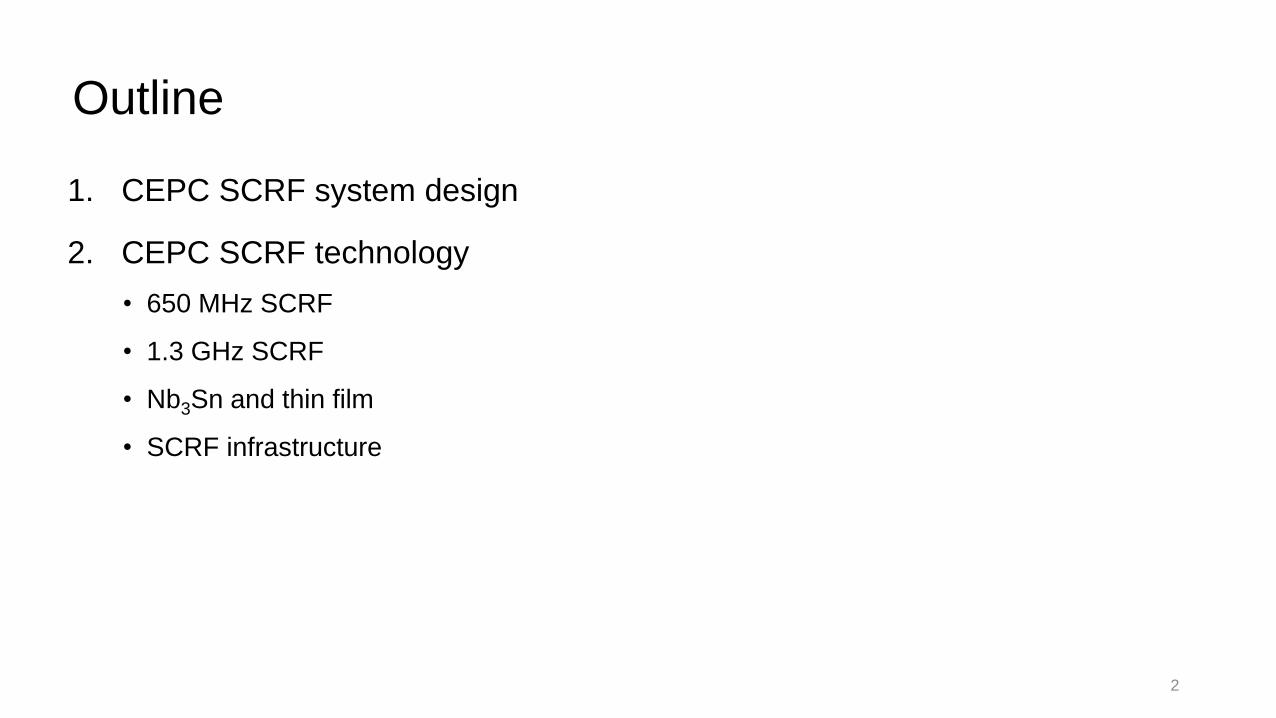
Outline
1. CEPC SCRF system design
2. CEPC SCRF technology
• 650 MHz SCRF
• 1.3 GHz SCRF
• Nb3Sn and thin film
• SCRF infrastructure
2
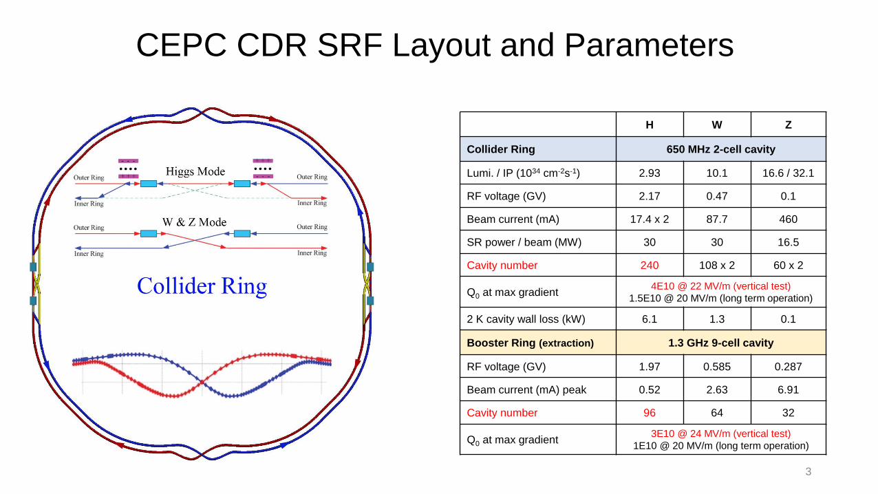
CEPC CDR SRF Layout and Parameters
H W Z
Collider Ring 650 MHz 2-cell cavity
Lumi. / IP (1034 cm-2s-1) 2.93 10.1 16.6 / 32.1
RF voltage (GV) 2.17 0.47 0.1
Beam current (mA) 17.4 x 2 87.7 460
SR power / beam (MW) 30 30 16.5
Cavity number 240 108 x 2 60 x 2
Q0 at max gradient4E10 @ 22 MV/m (vertical test)
1.5E10 @ 20 MV/m (long term operation)
2 K cavity wall loss (kW) 6.1 1.3 0.1
Booster Ring (extraction) 1.3 GHz 9-cell cavity
RF voltage (GV) 1.97 0.585 0.287
Beam current (mA) peak 0.52 2.63 6.91
Cavity number 96 64 32
Q0 at max gradient3E10 @ 24 MV/m (vertical test)
1E10 @ 20 MV/m (long term operation)
3

4
CEPC Collider Ring High Luminosity Parameters
20210115 tt Higgs W Z
Number of IPs 2 2 2 2
Energy (GeV) 180 120 80 45.5
Circumference (km) 100 100 100 100
SR loss/turn (GeV) 8.53 1.73 0.33 0.036
Half crossing angle (mrad) 16.5 16.5 16.5 16.5
Piwinski angle 1.16 4.87 9.12 24.9
Ne/bunch (1010) 20.1 16.3 11.6 15.2
Bunch number (bunch spacing) 37 (4.45s) 214 (0.7us) 1588 (0.2s) 3816 (86ns) 11498 (26ns)
Beam current (mA) 3.5 16.8 88.5 278.8 839.9
SR power / beam (MW) 30 30 30 10 30
Bending radius (km) 10.7 10.7 10.7 10.7
Phase advance of arc cell 90/90 90/90 90/90 60/60
Momentum compaction (10-5) 0.73 0.73 0.73 1.48
IP x/y (m) 1.0/0.0027 0.33/0.001 0.33/0.001 0.15/0.001
Emittance x/y (nm) 1.45/0.0047 0.68/0.0014 0.28/0.00084 0.27/0.00135
Transverse IP (um) 37.9/0.11 15.0/0.037 9.6/0.029 6.36/0.037
x/y/IP 0.076/0.106 0.018/0.115 0.014/0.13 0.0046/0.131
VRF (GV) 9.52 2.27 0.47 0.1
f RF (MHz) (harmonic) 650 (216816) 650 (216816) 650 (216816) 650 (216816)
Nature bunch length z (mm) 2.23 2.25 2.4 2.75
Bunch length z (mm) 2.66 4.42 5.3 9.6
HOM power/cavity (kw) 0.45 (5cell) 0.48 (2cell) 0.79 (2cell) 2.0 (2cell) 3.02 (1cell)
Energy spread (%) 0.17 0.19 0.11 0.12
Energy acceptance requirement (DA)
(%)2.0 1.7 1.2 1.3
Energy acceptance by RF (%) 2.61 2.5 1.83 1.48
Lifetime (hour) 0.59 0.35 1.3 1.7 1.4
Lmax/IP (1034cm-2s-1) 0.5 5.0 18.7 35.0 105.5
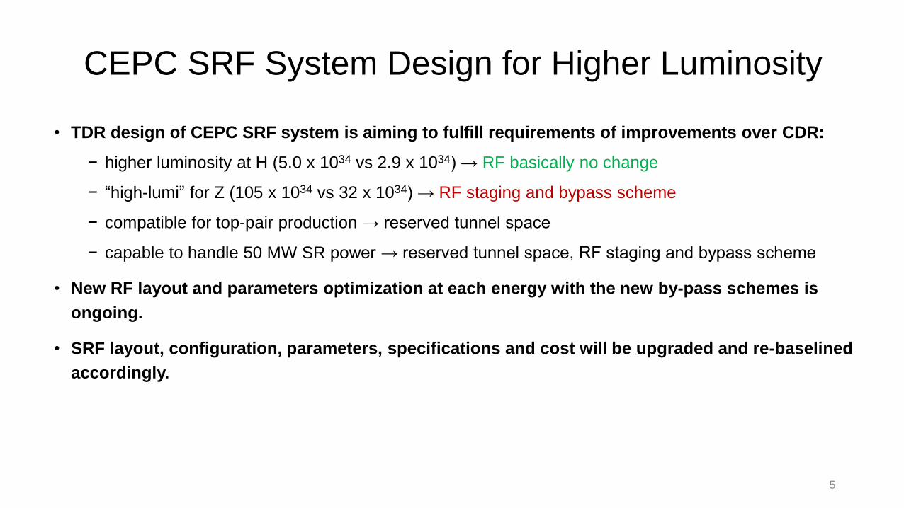
CEPC SRF System Design for Higher Luminosity
• TDR design of CEPC SRF system is aiming to fulfill requirements of improvements over CDR:
− higher luminosity at H (5.0 x 1034 vs 2.9 x 1034) → RF basically no change
− “high-lumi” for Z (105 x 1034 vs 32 x 1034) → RF staging and bypass scheme
− compatible for top-pair production → reserved tunnel space
− capable to handle 50 MW SR power → reserved tunnel space, RF staging and bypass scheme
• New RF layout and parameters optimization at each energy with the new by-pass schemes is
ongoing.
• SRF layout, configuration, parameters, specifications and cost will be upgraded and re-baselined
accordingly.
5

New RF Staging & By-pass Scheme for CEPC
Stage 1 (H/W run for 8 years): keep CDR RF layout for H/W and 50 MW
upgrade. Common cavities for H. Separate cavities for W/Z. Z initial
operation for energy calibration and could reach CDR luminosity.
Minimize first phase construction cost and hold Higgs priority.
Stage 2 (HL-Z upgrade): move Higgs cavities to center, add 2x100 MV
650 MHz high current Z cavities (international sharing for modules and
RF sources). By-pass low current H cavities.
Stage 3 (ttbar upgrade): add ttbar cavities (international sharing):
Collider + 7 GV 650 MHz 5-cell cavity, Booster + 6 GV 1.3 GHz 9-cell
cavity. Both low current, high gradient, high Q. [email protected] K or others.
• Unleash full potential of CEPC with operational flexibility.
• Seamless mode switching with unrestricted RF performance at
each energy until AC power limit.
• Stepwise construction cost, technology risk and international
involvement.
6
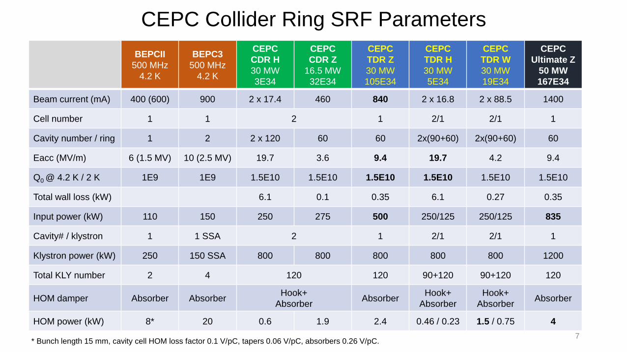
CEPC Collider Ring SRF Parameters
7
BEPCII
500 MHz
4.2 K
BEPC3
500 MHz
4.2 K
CEPC
CDR H
30 MW
3E34
CEPC
CDR Z
16.5 MW
32E34
CEPC
TDR Z
30 MW
105E34
CEPC
TDR H
30 MW
5E34
CEPC
TDR W
30 MW
19E34
CEPC
Ultimate Z
50 MW
167E34
Beam current (mA) 400 (600) 900 2 x 17.4 460 840 2 x 16.8 2 x 88.5 1400
Cell number 1 1 2 1 2/1 2/1 1
Cavity number / ring 1 2 2 x 120 60 60 2x(90+60) 2x(90+60) 60
Eacc (MV/m) 6 (1.5 MV) 10 (2.5 MV) 19.7 3.6 9.4 19.7 4.2 9.4
Q0 @ 4.2 K / 2 K 1E9 1E9 1.5E10 1.5E10 1.5E10 1.5E10 1.5E10 1.5E10
Total wall loss (kW) 6.1 0.1 0.35 6.1 0.27 0.35
Input power (kW) 110 150 250 275 500 250/125 250/125 835
Cavity# / klystron 1 1 SSA 2 1 2/1 2/1 1
Klystron power (kW) 250 150 SSA 800 800 800 800 800 1200
Total KLY number 2 4 120 120 90+120 90+120 120
HOM damper Absorber AbsorberHook+
AbsorberAbsorber
Hook+
Absorber
Hook+
AbsorberAbsorber
HOM power (kW) 8* 20 0.6 1.9 2.4 0.46 / 0.23 1.5 / 0.75 4
* Bunch length 15 mm, cavity cell HOM loss factor 0.1 V/pC, tapers 0.06 V/pC, absorbers 0.26 V/pC.
8
Will update Booster 1.3 GHz RF parameters
accordingly.
Outline
1. CEPC SCRF system design
2. CEPC SCRF technology
• 650 MHz SCRF
• 1.3 GHz SCRF
• Nb3Sn and thin film
• SCRF infrastructure
9

CEPC SRF System TDR Status and Plan
TDR Phase 1: 2019-2020 (System Design, Components Prototyping)
✓ SRF system TDR design for higher luminosity (RF staging and bypass scheme proposed)
✓ High Q, high gradient cavity, high power components and other key technology R&D (close to CEPC spec)
✓ PAPS SRF facility construction (equipment installation)
TDR Phase 2: 2021-2022 (System Design, Cryomodule Prototyping)
SRF system TDR design re-baseline and optimization
650 MHz high Q short cryomodule assembly, operation and improvement (to meet CEPC spec)
1.3 GHz high Q full cryomodule prototyping (to meet CEPC and CW FEL spec)
Nb3Sn and other thin film cavity R&D
SRF facility (PAPS commissioning, operation and upgrade)
Post-TDR: 2023-2025 (Cryomodule Prototyping, Mass-Production Preparation)
• SRF system Engineering Design, mass-production technology preparation
• 650 MHz full cryomodule prototyping
• 1.3 GHz high Q full cryomodule industrialization and mass production (for FEL projects)
• 650 MHz Z-pole high current cryomodule and ttbar cryomodule concept design
• Nb3Sn cavity and cryomodule prototyping10
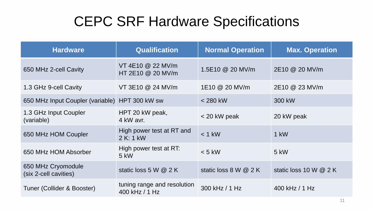
CEPC SRF Hardware Specifications
11
Hardware Qualification Normal Operation Max. Operation
650 MHz 2-cell CavityVT 4E10 @ 22 MV/m
HT 2E10 @ 20 MV/m1.5E10 @ 20 MV/m 2E10 @ 20 MV/m
1.3 GHz 9-cell Cavity VT 3E10 @ 24 MV/m 1E10 @ 20 MV/m 2E10 @ 23 MV/m
650 MHz Input Coupler (variable) HPT 300 kW sw < 280 kW 300 kW
1.3 GHz Input Coupler
(variable)
HPT 20 kW peak,
4 kW avr.< 20 kW peak 20 kW peak
650 MHz HOM CouplerHigh power test at RT and
2 K: 1 kW< 1 kW 1 kW
650 MHz HOM AbsorberHigh power test at RT:
5 kW< 5 kW 5 kW
650 MHz Cryomodule
(six 2-cell cavities)static loss 5 W @ 2 K static loss 8 W @ 2 K static loss 10 W @ 2 K
Tuner (Collider & Booster)tuning range and resolution
400 kHz / 1 Hz300 kHz / 1 Hz 400 kHz / 1 Hz
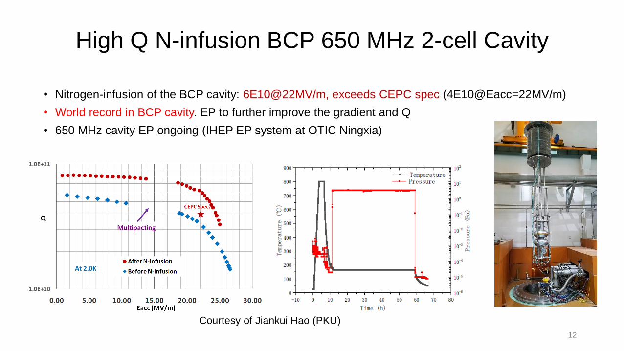
High Q N-infusion BCP 650 MHz 2-cell Cavity
• Nitrogen-infusion of the BCP cavity: 6E10@22MV/m, exceeds CEPC spec (4E10@Eacc=22MV/m)
• World record in BCP cavity. EP to further improve the gradient and Q
• 650 MHz cavity EP ongoing (IHEP EP system at OTIC Ningxia)
12
Courtesy of Jiankui Hao (PKU)
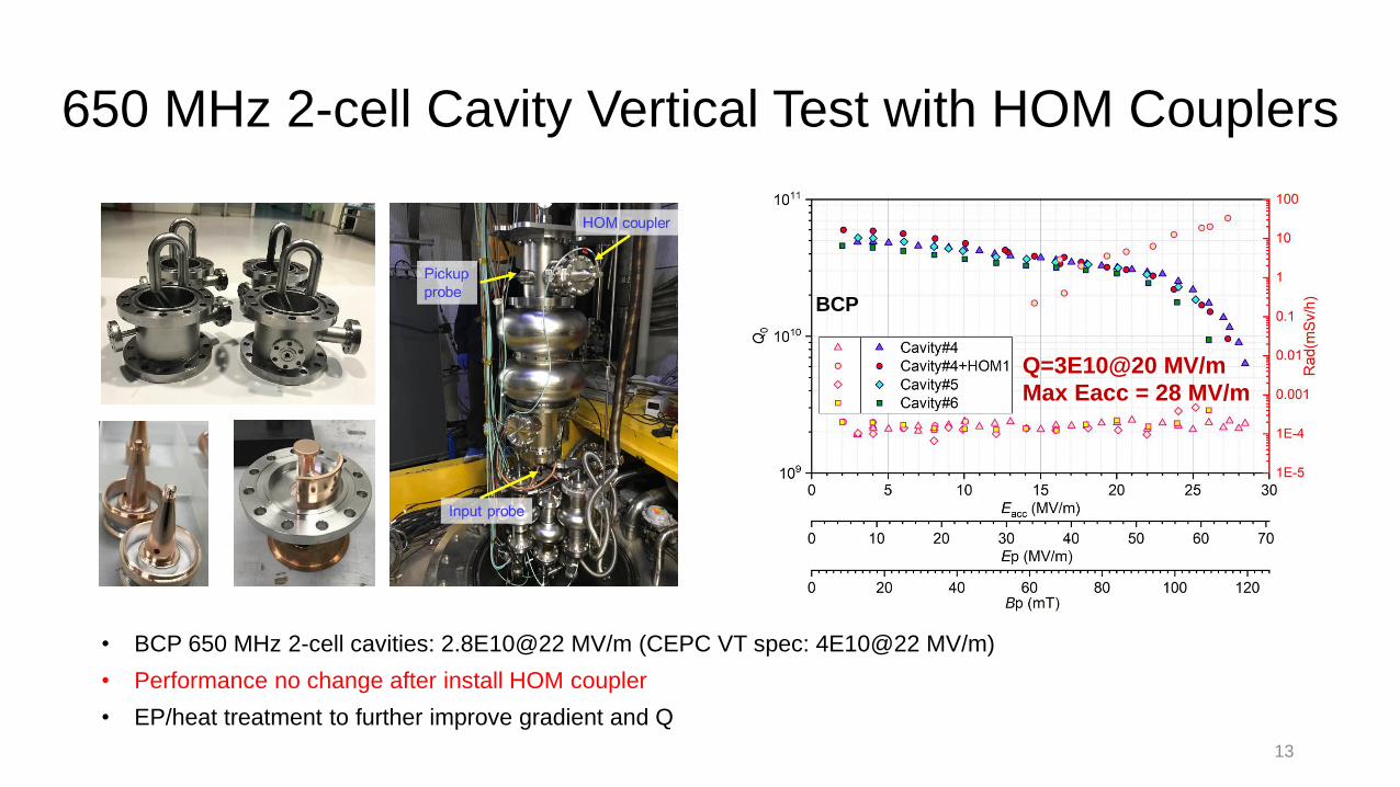
650 MHz 2-cell Cavity Vertical Test with HOM Couplers
• BCP 650 MHz 2-cell cavities: 2.8E10@22 MV/m (CEPC VT spec: 4E10@22 MV/m)
• Performance no change after install HOM coupler
• EP/heat treatment to further improve gradient and Q
BCP
13
Q=3E10@20 MV/m
Max Eacc = 28 MV/m
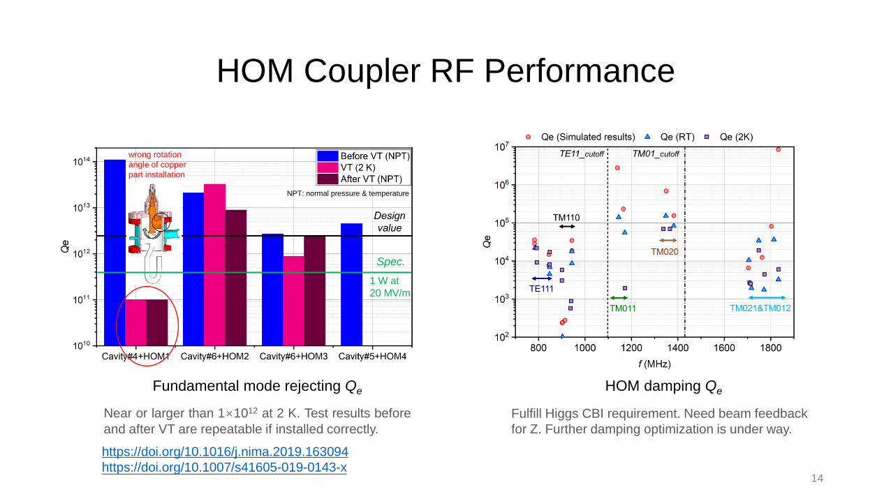
HOM Coupler RF Performance
Fundamental mode rejecting Qe
Near or larger than 1×10¹² at 2 K. Test results before
and after VT are repeatable if installed correctly.
HOM damping Qe
Fulfill Higgs CBI requirement. Need beam feedback
for Z. Further damping optimization is under way.
wrong rotation
angle of copper
part installation
NPT: normal pressure & temperature
Spec.
1 W at
20 MV/m
14
https://doi.org/10.1016/j.nima.2019.163094
https://doi.org/10.1007/s41605-019-0143-x

Cavity Dressing
15
Vertical test of 2-cell cavities with helium vessel and HOM couplers ongoing.

Preserve Q0 in Module: Magnetic Shielding and Compensating
North
Because of beam direction and larger beam pipe than
1.3 GHz, only two shieldings can reach the magnetic
field requirement of high Q 650 MHz cavity: cavity (2
K local) shield and module (RT global) shield.
𝑅m𝑎𝑔 = 𝜂 ∙ 𝑆(𝑙) ∙ (𝐵ext+𝐵tc) 𝑓
1. Flux trapping ratio: grain size, high-T annealing, fast cold down
2. Magnetic sensitivity: mean free path and other
3. Remnant magnetic field: demagnetization, magnetic shield,
magnetic compensation
4. Thermocurrent induced magnetic fieldMagnetic compensation with coils
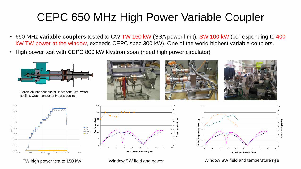
CEPC 650 MHz High Power Variable Coupler
• 650 MHz variable couplers tested to CW TW 150 kW (SSA power limit), SW 100 kW (corresponding to 400
kW TW power at the window, exceeds CEPC spec 300 kW). One of the world highest variable couplers.
• High power test with CEPC 800 kW klystron soon (need high power circulator)
Window SW field and power Window SW field and temperature riseTW high power test to 150 kW
Bellow on inner conductor. Inner conductor water
cooling. Outer conductor He gas cooling.
17
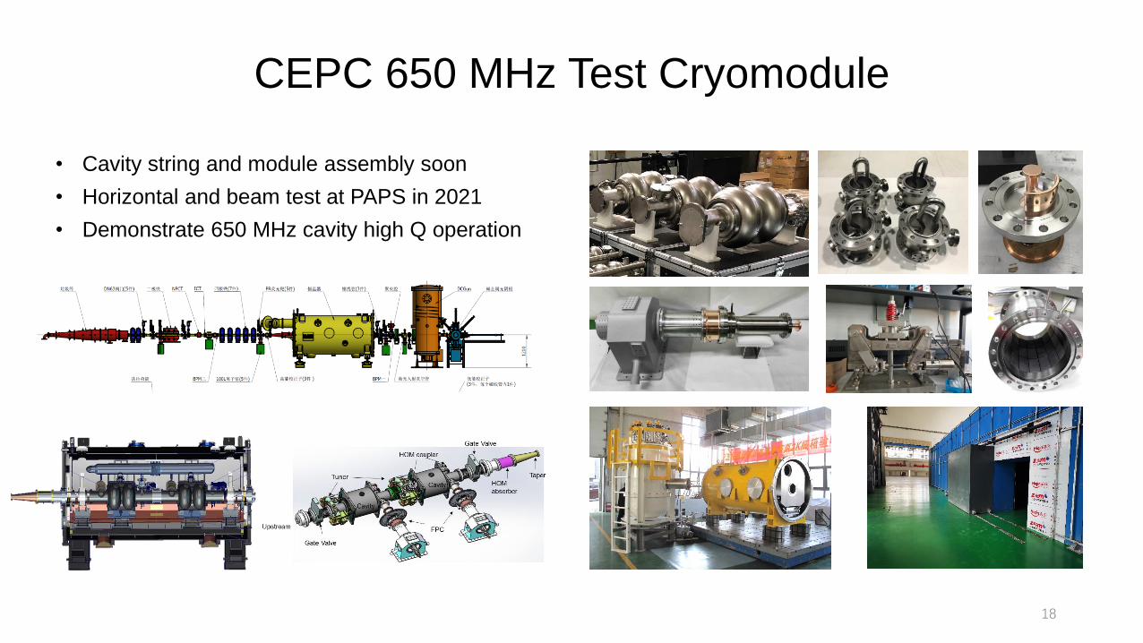
CEPC 650 MHz Test Cryomodule
• Cavity string and module assembly soon
• Horizontal and beam test at PAPS in 2021
• Demonstrate 650 MHz cavity high Q operation
18
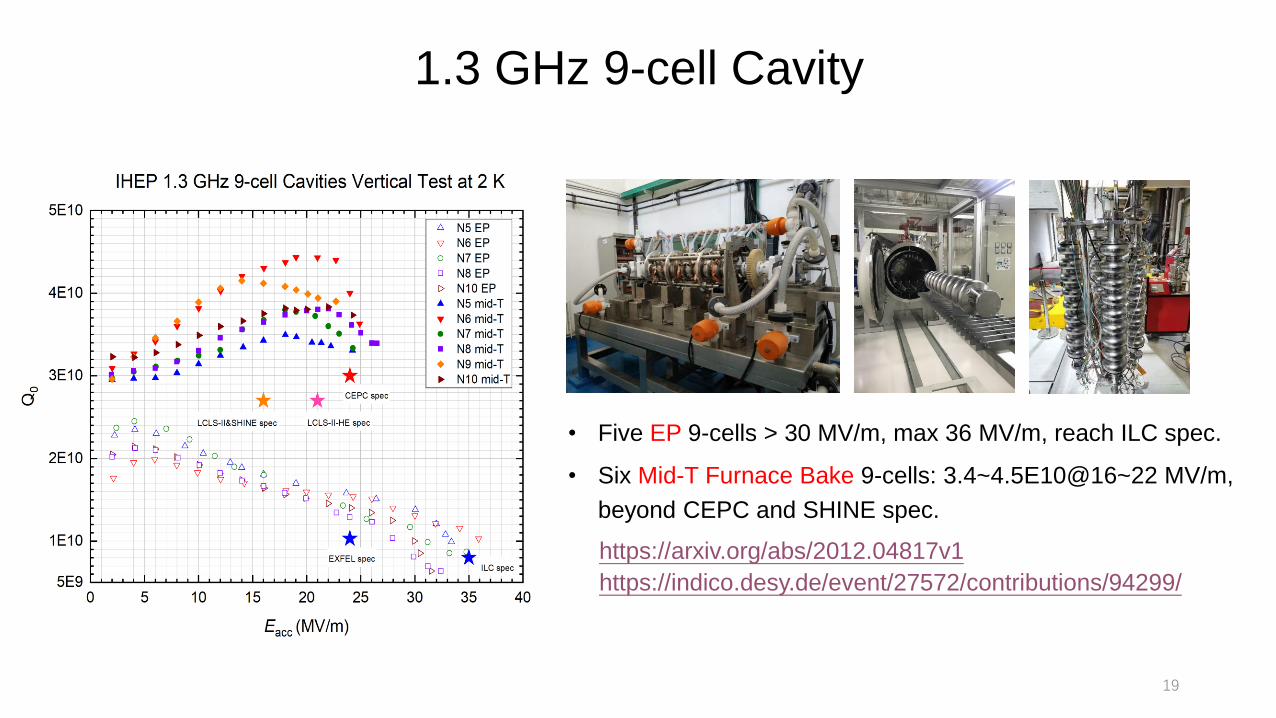
1.3 GHz 9-cell Cavity
19
https://arxiv.org/abs/2012.04817v1
https://indico.desy.de/event/27572/contributions/94299/
• Five EP 9-cells > 30 MV/m, max 36 MV/m, reach ILC spec.
• Six Mid-T Furnace Bake 9-cells: 3.4~4.5E10@16~22 MV/m,
beyond CEPC and SHINE spec.
1.3 GHz Input Coupler
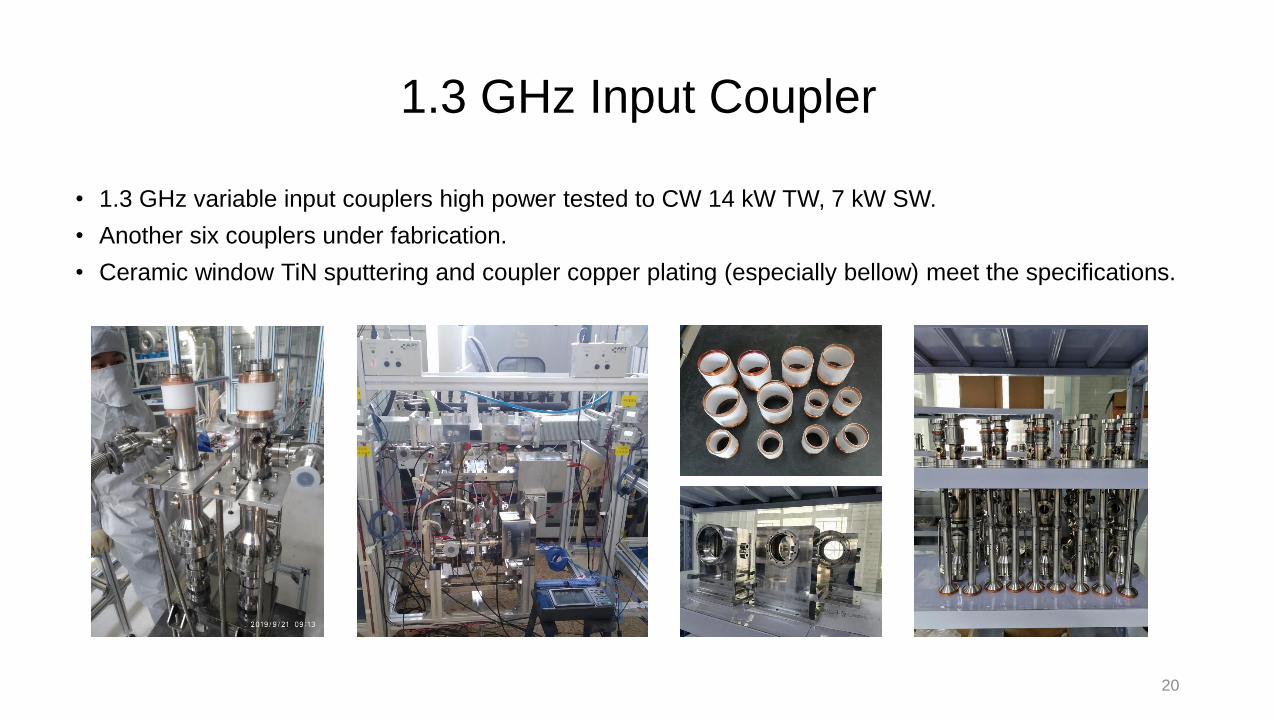
• 1.3 GHz variable input couplers high power tested to CW 14 kW TW, 7 kW SW.
• Another six couplers under fabrication.
• Ceramic window TiN sputtering and coupler copper plating (especially bellow) meet the specifications.
20
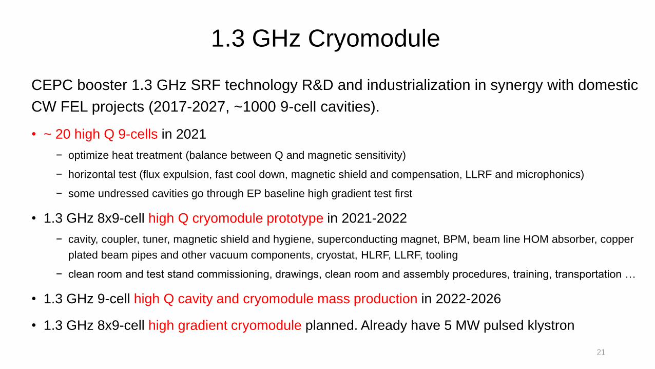
1.3 GHz Cryomodule
CEPC booster 1.3 GHz SRF technology R&D and industrialization in synergy with domestic
CW FEL projects (2017-2027, ~1000 9-cell cavities).
• ~ 20 high Q 9-cells in 2021
− optimize heat treatment (balance between Q and magnetic sensitivity)
− horizontal test (flux expulsion, fast cool down, magnetic shield and compensation, LLRF and microphonics)
− some undressed cavities go through EP baseline high gradient test first
• 1.3 GHz 8x9-cell high Q cryomodule prototype in 2021-2022
− cavity, coupler, tuner, magnetic shield and hygiene, superconducting magnet, BPM, beam line HOM absorber, copper
plated beam pipes and other vacuum components, cryostat, HLRF, LLRF, tooling
− clean room and test stand commissioning, drawings, clean room and assembly procedures, training, transportation …
• 1.3 GHz 9-cell high Q cavity and cryomodule mass production in 2022-2026
• 1.3 GHz 8x9-cell high gradient cryomodule planned. Already have 5 MW pulsed klystron
21
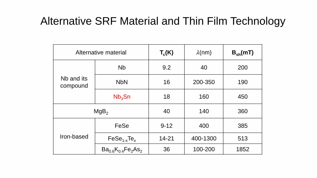
Alternative SRF Material and Thin Film Technology
Alternative material Tc(K) 𝜆(nm) Bsh(mT)
Nb and its
compound
Nb 9.2 40 200
NbN 16 200-350 190
Nb3Sn 18 160 450
MgB2 40 140 360
Iron-based
FeSe 9-12 400 385
FeSe1-xTex 14-21 400-1300 513
Ba0.6K0.4Fe2As2 36 100-200 1852

Nb3Sn/Nb Coating (Vapor Diffusion)
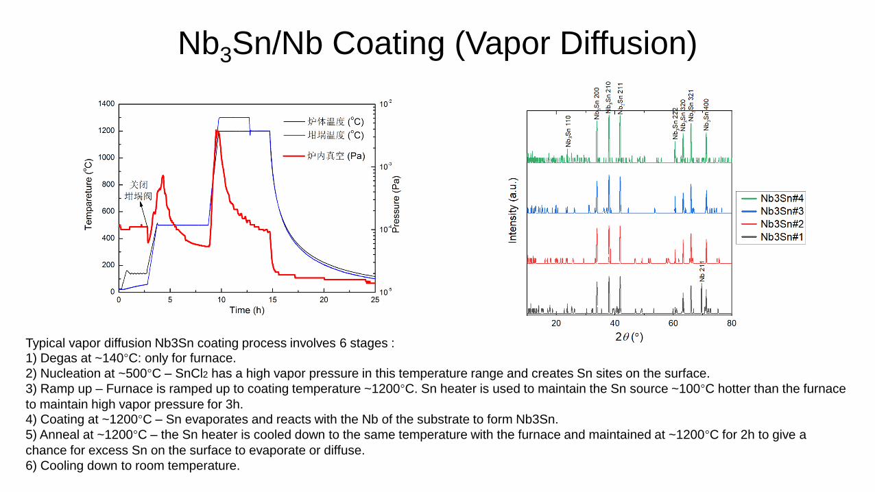
Nb3Sn/Nb Coating (Vapor Diffusion)
Typical vapor diffusion Nb3Sn coating process involves 6 stages :1) Degas at ~140°C: only for furnace.
2) Nucleation at ~500°C – SnCl2 has a high vapor pressure in this temperature range and creates Sn sites on the surface.
3) Ramp up – Furnace is ramped up to coating temperature ~1200°C. Sn heater is used to maintain the Sn source ~100°C hotter than the furnace
to maintain high vapor pressure for 3h.4) Coating at ~1200°C – Sn evaporates and reacts with the Nb of the substrate to form Nb3Sn.
5) Anneal at ~1200°C – the Sn heater is cooled down to the same temperature with the furnace and maintained at ~1200°C for 2h to give a
chance for excess Sn on the surface to evaporate or diffuse.
6) Cooling down to room temperature.
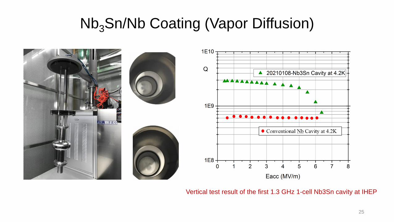
Nb3Sn/Nb Coating (Vapor Diffusion)
25
Vertical test result of the first 1.3 GHz 1-cell Nb3Sn cavity at IHEP
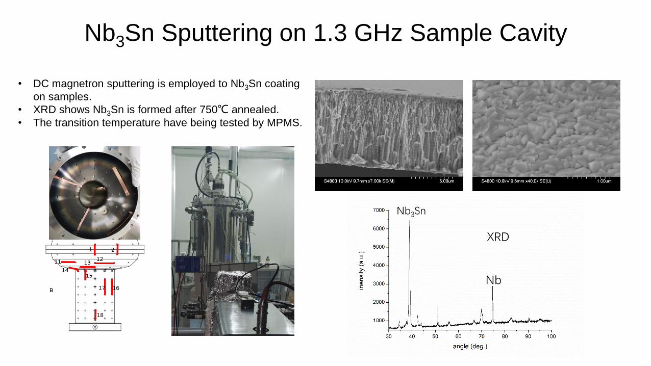
Nb3Sn Sputtering on 1.3 GHz Sample Cavity
• DC magnetron sputtering is employed to Nb3Sn coating
on samples.
• XRD shows Nb3Sn is formed after 750℃ annealed.
• The transition temperature have being tested by MPMS.
XRD
Nb3Sn
Nb
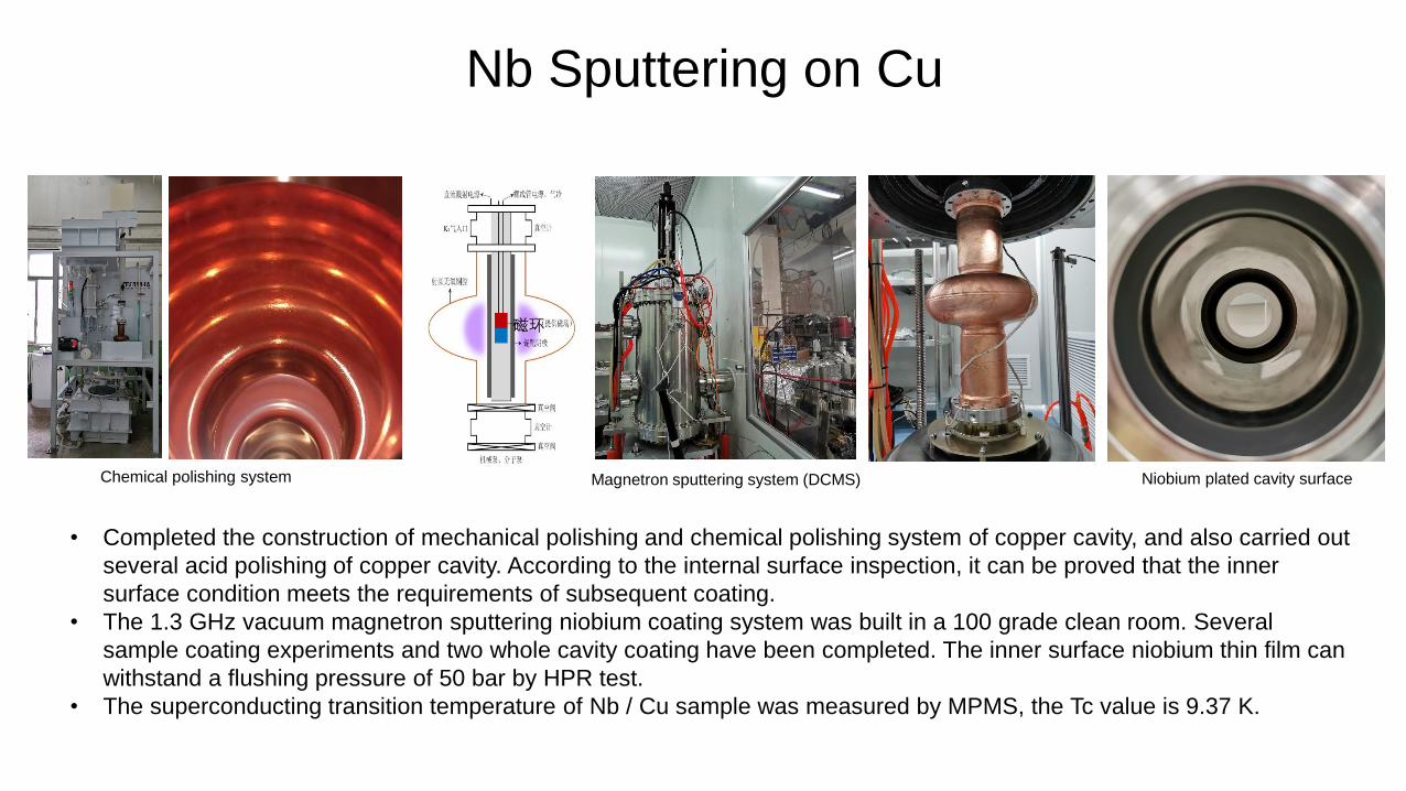
Chemical polishing system Magnetron sputtering system (DCMS) Niobium plated cavity surface
• Completed the construction of mechanical polishing and chemical polishing system of copper cavity, and also carried out
several acid polishing of copper cavity. According to the internal surface inspection, it can be proved that the inner
surface condition meets the requirements of subsequent coating.
• The 1.3 GHz vacuum magnetron sputtering niobium coating system was built in a 100 grade clean room. Several
sample coating experiments and two whole cavity coating have been completed. The inner surface niobium thin film can
withstand a flushing pressure of 50 bar by HPR test.
• The superconducting transition temperature of Nb / Cu sample was measured by MPMS, the Tc value is 9.37 K.
Nb Sputtering on Cu
磁环
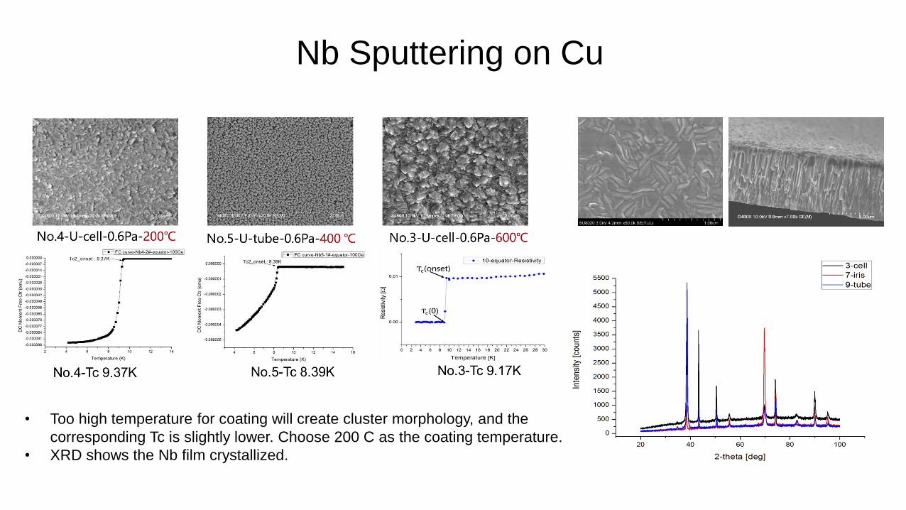
• Too high temperature for coating will create cluster morphology, and the
corresponding Tc is slightly lower. Choose 200 C as the coating temperature.
• XRD shows the Nb film crystallized.
Nb Sputtering on Cu
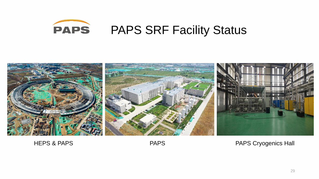
29
PAPS SRF Facility Status
HEPS & PAPS PAPS PAPS Cryogenics Hall
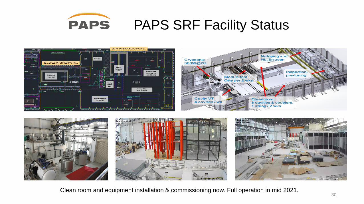
PAPS SRF Facility Status
Clean room and equipment installation & commissioning now. Full operation in mid 2021.30
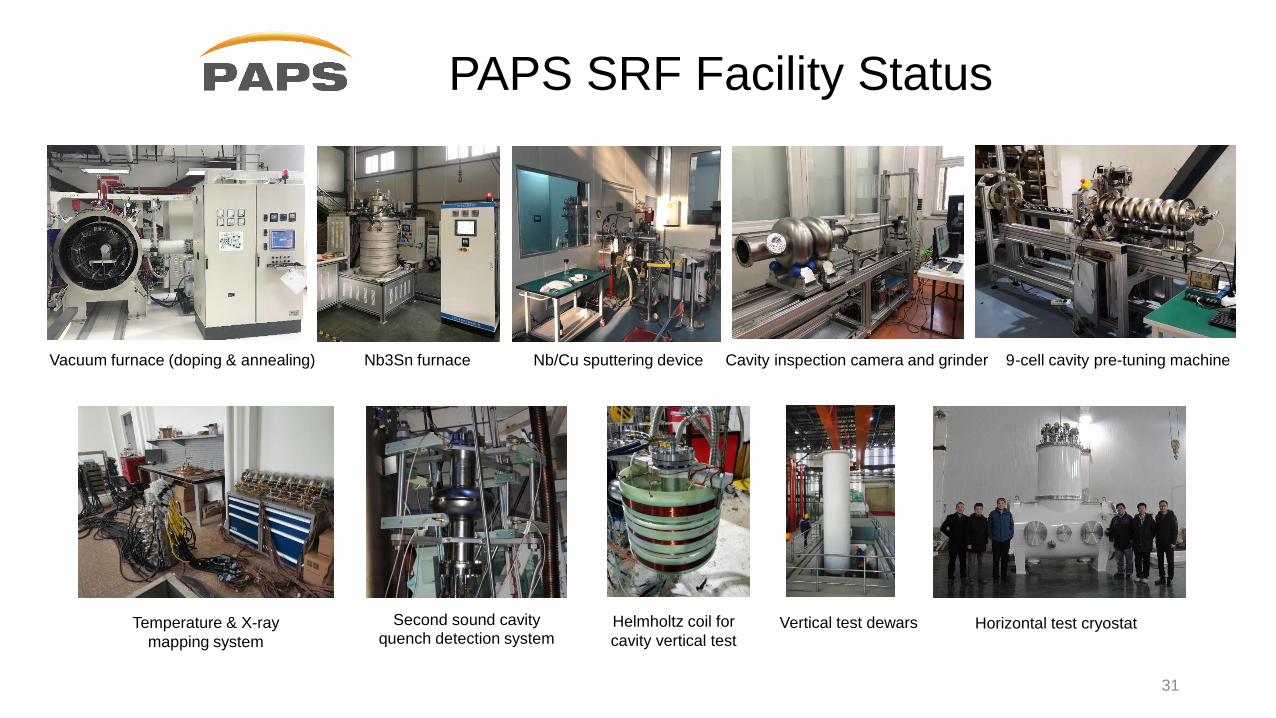
PAPS SRF Facility Status
Vacuum furnace (doping & annealing) Nb3Sn furnace Nb/Cu sputtering device Cavity inspection camera and grinder 9-cell cavity pre-tuning machine
Temperature & X-ray
mapping system
Second sound cavity quench detection system
Helmholtz coil for
cavity vertical testVertical test dewars Horizontal test cryostat
31
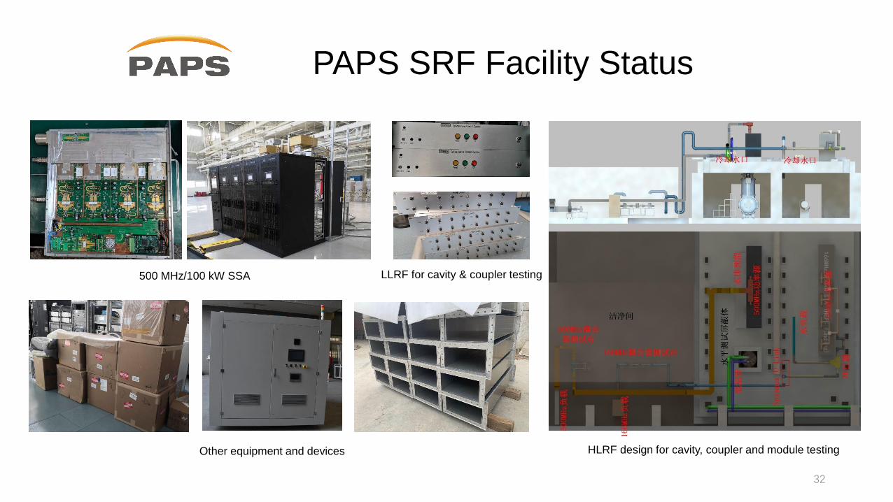
LLRF for cavity & coupler testing
PAPS SRF Facility Status
500 MHz/100 kW SSA
HLRF design for cavity, coupler and module testingOther equipment and devices
32
Summary
• CEPC SRF system design and technology R&D towards TDR. RF cavity by-pass
scheme enable cost staging, mode switching and full potential of CEPC.
• Progress in 650 MHz and 1.3 GHz cavity and other key technology. 650 MHz test
module in 2021. Thin film (Nb3Sn etc) for the future SRF.
• Full speed for 1.3 GHz cryomodule in next 5 years. Critical for SCRF technology,
expertise and industrialization.
• PAPS SRF infrastructure at Huairou will start operation in mid 2021 to support R&D.
33

Thank you for your time34